Light emitting diode light source device
Hsu , et al. December 30, 2
U.S. patent number 8,921,880 [Application Number 13/729,044] was granted by the patent office on 2014-12-30 for light emitting diode light source device. This patent grant is currently assigned to Advanced Optoelectronics Technology, Inc.. The grantee listed for this patent is Advanced Optoelectronic Technology, Inc.. Invention is credited to Chien-Lin Chang-Chien, Chung-Min Chang, Chih-Peng Hsu, Hsuen-Feng Hu, Yu-Wei Tsai.


| United States Patent | 8,921,880 |
| Hsu , et al. | December 30, 2014 |
| **Please see images for: ( Certificate of Correction ) ** |
Light emitting diode light source device
Abstract
An LED light source device includes an LED light source, a first translucent structure covering the LED light source and a second translucent structure covering the first translucent structure. An interior of the first translucent structure has light scattering powder distributed therein. The LED light source is embedded in the first translucent structure. The LED light source is covered by the light scattering powder. The second translucent structure has a radius of R and an index of refraction of N.sub.1, while the first translucent structure has a radius of r, wherein R, r and N.sub.1 satisfy the following relation: N.sub.1<R/(2r-R).
| Inventors: | Hsu; Chih-Peng (Hsinchu, TW), Chang; Chung-Min (Hsinchu, TW), Hu; Hsuen-Feng (Hsinchu, TW), Chang-Chien; Chien-Lin (Hsinchu, TW), Tsai; Yu-Wei (Hsinchu, TW) | ||||||||||
|---|---|---|---|---|---|---|---|---|---|---|---|
| Applicant: |
|
||||||||||
| Assignee: | Advanced Optoelectronics
Technology, Inc. (Hsinchu Hsien, TW) |
||||||||||
| Family ID: | 49461259 | ||||||||||
| Appl. No.: | 13/729,044 | ||||||||||
| Filed: | December 28, 2012 |
Prior Publication Data
| Document Identifier | Publication Date | |
|---|---|---|
| US 20130285094 A1 | Oct 31, 2013 | |
| Current U.S. Class: | 257/98; 362/311.06; 362/311.02 |
| Current CPC Class: | H01L 33/50 (20130101); H01L 33/56 (20130101); H01L 33/505 (20130101); H01L 33/54 (20130101); H01L 2933/0091 (20130101) |
| Current International Class: | H01L 33/50 (20100101) |
| Field of Search: | ;313/502 ;362/311.06,311.07,311.08,311.09,311.1 |
References Cited [Referenced By]
U.S. Patent Documents
| 6155699 | December 2000 | Miller et al. |
| 6204523 | March 2001 | Carey et al. |
| 6252254 | June 2001 | Soules et al. |
| 6294800 | September 2001 | Duggal et al. |
| 6296376 | October 2001 | Kondo et al. |
| 6560038 | May 2003 | Parkyn et al. |
| 6580097 | June 2003 | Soules et al. |
| 6803719 | October 2004 | Miller et al. |
| 6914265 | July 2005 | Bawendi et al. |
| 7005679 | February 2006 | Tarsa et al. |
| 7049740 | May 2006 | Takekuma |
| 7119376 | October 2006 | Liu et al. |
| 7227190 | June 2007 | Yasukawa et al. |
| 7332746 | February 2008 | Takahashi et al. |
| 7374807 | May 2008 | Parce et al. |
| 7420219 | September 2008 | Kang et al. |
| 7479662 | January 2009 | Soules et al. |
| 7531956 | May 2009 | Kim et al. |
| 7592639 | September 2009 | Maeda et al. |
| 7629620 | December 2009 | Maeda et al. |
| 7658866 | February 2010 | Murazaki et al. |
| 7663315 | February 2010 | Hulse |
| 7679281 | March 2010 | Kim et al. |
| 7709852 | May 2010 | Hohn et al. |
| 7710016 | May 2010 | Miki et al. |
| 7745818 | June 2010 | Sofue et al. |
| 7753553 | July 2010 | Justel et al. |
| 7772604 | August 2010 | Duong et al. |
| 7800124 | September 2010 | Urano et al. |
| RE41807 | October 2010 | Yokoi et al. |
| 7828453 | November 2010 | Tran et al. |
| 7858997 | December 2010 | Yoshimura et al. |
| 7858998 | December 2010 | Negley |
| 7923918 | April 2011 | Tamaki et al. |
| 7960909 | June 2011 | Amano et al. |
| 7985015 | July 2011 | Tasch et al. |
| 7989236 | August 2011 | Yamaguchi et al. |
| 8025429 | September 2011 | Ho et al. |
| 8044424 | October 2011 | Urano et al. |
| 8067884 | November 2011 | Li |
| 8071996 | December 2011 | Hohn et al. |
| 8125139 | February 2012 | Emoto et al. |
| 8163203 | April 2012 | Im et al. |
| 8168998 | May 2012 | David et al. |
| 8240888 | August 2012 | Zhang et al. |
| 8272768 | September 2012 | Kazmierski et al. |
| 8308980 | November 2012 | Lee et al. |
| 8318044 | November 2012 | Lee et al. |
| 8322896 | December 2012 | Falicoff et al. |
| 8328395 | December 2012 | Kato et al. |
| 8382337 | February 2013 | Ing et al. |
| 8419229 | April 2013 | Dong |
| 8430538 | April 2013 | Holder et al. |
| 8449150 | May 2013 | Allen et al. |
| 8511864 | August 2013 | Holder et al. |
| 8536608 | September 2013 | David et al. |
| 8545061 | October 2013 | Chang et al. |
| 8547009 | October 2013 | Hussell et al. |
| 8558446 | October 2013 | Miki et al. |
| 8558456 | October 2013 | Yokotani |
| 8562161 | October 2013 | Tong et al. |
| 8569944 | October 2013 | Choi et al. |
| 8573815 | November 2013 | Mallory et al. |
| 8602605 | December 2013 | Park et al. |
| 8616734 | December 2013 | Olsson |
| 8624289 | January 2014 | Wirth |
| 8641238 | February 2014 | Chiu et al. |
| 2004/0217692 | November 2004 | Cho et al. |
| 2005/0052871 | March 2005 | Leu et al. |
| 2005/0212397 | September 2005 | Murazaki et al. |
| 2006/0226758 | October 2006 | Sofue et al. |
| 2008/0143246 | June 2008 | Hirosaki et al. |
| 2008/0246044 | October 2008 | Pang |
| 2009/0189507 | July 2009 | Winkler et al. |
| 2009/0200939 | August 2009 | Lenk et al. |
| 2009/0272996 | November 2009 | Chakraborty |
| 2010/0084962 | April 2010 | Winkler et al. |
| 2010/0123386 | May 2010 | Chen |
| 2010/0140551 | June 2010 | Parce et al. |
| 2010/0181582 | July 2010 | Li et al. |
| 2010/0194263 | August 2010 | Winkler et al. |
| 2010/0201250 | August 2010 | Winkler et al. |
| 2010/0232134 | September 2010 | Tran |
| 2010/0308356 | December 2010 | Wirth |
| 2011/0001422 | January 2011 | Aanegola et al. |
| 2011/0006329 | January 2011 | Fujita et al. |
| 2011/0045619 | February 2011 | Ling |
| 2011/0069496 | March 2011 | Ing et al. |
| 2011/0085352 | April 2011 | Ito et al. |
| 2011/0133220 | June 2011 | Kim et al. |
| 2011/0149580 | June 2011 | Fu et al. |
| 2011/0180780 | July 2011 | Yoo et al. |
| 2011/0215700 | September 2011 | Tong et al. |
| 2011/0216523 | September 2011 | Tong et al. |
| 2011/0227475 | September 2011 | Winkler et al. |
| 2011/0248287 | October 2011 | Yuan et al. |
| 2011/0273083 | November 2011 | Yun et al. |
| 2011/0279011 | November 2011 | Murphy et al. |
| 2011/0279022 | November 2011 | Winkler et al. |
| 2011/0304261 | December 2011 | Winkler et al. |
| 2011/0309398 | December 2011 | Ito et al. |
| 2011/0316032 | December 2011 | Ooyabu et al. |
| 2012/0018754 | January 2012 | Lowes |
| 2012/0057327 | March 2012 | Le et al. |
| 2012/0068118 | March 2012 | Parce et al. |
| 2012/0212959 | August 2012 | Inoue et al. |
| 2013/0285094 | October 2013 | Hsu et al. |
| 102047452 | May 2011 | CN | |||
| 202009035 | Oct 2011 | CN | |||
Attorney, Agent or Firm: Novak Druce Connolly Bove + Quigg LLP
Claims
What is claimed is:
1. An LED light source device, comprising: an LED light source; a first translucent structure covering the LED light source, powder with a characteristic of scattering light being distributed in an interior of the first translucent structure, the LED light source being embedded in the first translucent structure and covered by the powder; and a second translucent structure covering the first translucent structure; wherein an outer contour of the first translucent structure and an outer contour of the second translucent structure are both partly spherical, the outer contour of the first translucent structure is coincident with a part of a first sphere, the outer contour of the second translucent structure is coincident with a part of a second sphere, and radiuses of the first sphere and the second sphere satisfy following condition: R>r, wherein r represents radius of the first sphere, R represents radius of the second sphere, and the first sphere for which the outer contour of the first translucent structure is partly coincidental is internally tangent with the second sphere for which the outer contour of the second translucent structure is partly coincidental, and wherein the index of refraction of the second translucent structure satisfies following condition: N.sub.1<R/(2r-R), wherein N.sub.1 represents the index of refraction of the second translucent structure.
2. The LED light source device of claim 1, wherein the LED light source is located on an extension line of a connecting line of the centers of the first translucent structure and the second translucent.
3. The LED light source device of claim 1, wherein the powder is made of phosphor materials.
4. The LED light source device of claim 1, wherein the powder is a mixture of phosphor materials and powder materials which include SiO.sub.2, Al.sub.2O.sub.3 or silicate.
5. The LED light source device of claim 1, wherein the powder is distributed in the interior of the whole first translucent structure evenly.
6. An LED light source device, comprising: an LED light source; a translucent structure located on a light path of the LED light source; powder filled in an interior of the translucent structure, the powder having a characteristic of scattering light; and wherein the LED light source is embedded in the translucent structure; wherein an outer contour of the translucent structure and an outer contour of the powder are both partly spherical, and the outer contour of the powder is coincident with a part of a first sphere, the outer contour of the translucent structure is coincident with a part of a second sphere, and radiuses of the first sphere and the second sphere satisfy following condition: R>r, wherein r represents radius of the first sphere, R represents radius of the second sphere, and the first sphere for which the outer contour of the powder is partly coincidental is internally tangent with the second sphere for which the outer contour of the translucent structure is partly coincidental; and wherein the index of refraction of the translucent structure satisfies following condition: N.sub.1<R/(2r-R), wherein N.sub.1 represents the index of refraction of the translucent structure.
7. The LED light source device of claim 6, wherein the LED light source is located on an extension line of a connecting line of the centers of the translucent structure and the powder.
8. The LED light source device of claim 6, wherein the powder is made of phosphor materials.
9. The LED light source device of claim 6, wherein the powder is a mixture of phosphor materials and powder materials which include SiO.sub.2, Al.sub.2O.sub.3 or silicate.
Description
BACKGROUND
1. Technical Field
The present disclosure relates to an LED (light emitting diode) light source device, and more particularly to an LED light source device having a uniform light distribution and a large viewing angle.
2. Description of Related Art
LEDs have been widely promoted as light sources of electronic devices owing to many advantages, such as high luminosity, low operational voltage and low power consumption. However, as a point light source, a viewing angle of the LED is only about 120.degree., and a light field of the LED is not uniform.
Therefore, an LED light source device capable of overcoming the above described shortcomings is desired.
BRIEF DESCRIPTION OF THE DRAWINGS
Many aspects of the present disclosure can be better understood with reference to the following drawings. The components in the drawings are not necessarily drawn to scale, the emphasis instead being placed upon clearly illustrating the principles of the present disclosure. Moreover, in the drawings, like reference numerals designate corresponding parts throughout the several views.
FIG. 1 shows a schematic view of an LED light source device in accordance with an embodiment of the present disclosure.
FIG. 2 shows a geometric diagram of a first translucent structure and a second translucent structure of the LED light source device illustrated in FIG. 1 of the present disclosure.
DETAILED DESCRIPTION
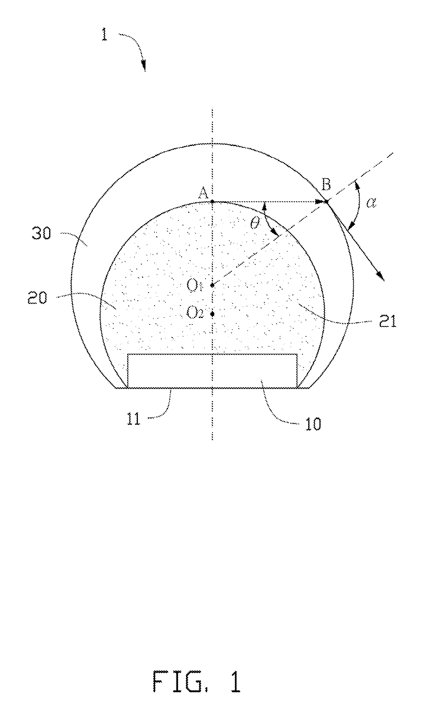
Referring to FIG. 1, an LED light source device 1 in accordance with an exemplary embodiment of the present disclosure includes an LED light source 10, a first translucent structure 20 covering the LED light source 10, and a second translucent structure 30 covering the first translucent structure 20.
In this embodiment, the LED light source 10 is an LED package, and includes a bottom surface 11. The LED light source 10 can also be an LED chip.
The first translucent structure 20 is located on a light path of the LED light source 10, and a kind of powder 21 with a characteristic of scattering light is distributed in an interior of the whole first translucent structure 20 evenly. Referring to FIG. 2, in this embodiment, the first translucent structure 20 is partly spherical. The LED light source 10 is embedded in the first translucent structure 20, merely with the bottom surface 11 exposed outside and coplanar with a bottom edge of the first translucent structure 20. Alternatively, the LED light source 10 can also be located outside of the first translucent structure 20, and the powder 21 can also be merely coated at an outer surface of the first translucent structure 20.
The second translucent structure 30 covers the first translucent structure 20 therebelow, and attaches to an outer surface of the first translucent structure 20. In this embodiment, the second translucent structure 30 is a lens, and the outer contour of the second translucent structure 30 is partly spherical. The first translucent structure 20 is embedded in the second translucent structure 30, and the bottom surface 11 of the LED light source 10 is coplanar with a bottom edge the second translucent structure 30. The index of refraction of the second translucent structure 30 is represented by N.sub.1.
Referring to FIG. 2, it shows a geometric diagram of the first translucent structure 20 and the second translucent structure 30. Sphere M and sphere N are defined, and the centers and radius of the sphere M and sphere N are illustrated and represented by point O.sub.2, point O.sub.1, r and R, respectively, and R>r. The sphere M is internally tangent with the sphere N at a point C. An outer contour of the first translucent structure 20 is coincident with a part of the sphere M, and an outer contour of the second translucent structure 30 is coincident with a part of the sphere N. The point C is located on an extension line of O.sub.1 O.sub.2 and away from the point O.sub.1. The extension line of O.sub.1 O.sub.2 and the sphere M intersect at a point A. The LED light source 10 is located on the extension line of O.sub.1 O.sub.2, and above the point C.
During operation of the LED light source 10, the light emitted from the LED light source 10 travels toward the first translucent structure 20. Under light scattering of the powder 21, the light output by the first translucent structure 20 will enter the second transparent structure 30 along various travelling directions. Therefore, the viewing angle of the LED light source device 1 is increased, and the light field of the LED light source device 1 is modified to be uniform. When light travelling from the point A to a point B on the outer contour of the second translucent structure 30, along a direction perpendicular to the line O.sub.1 O.sub.2, strikes onto the outer contour of the second translucent structure 30, an incident angle thereof is defined as .theta.. A critical angle of total reflection of the outer contour of the second translucent structure 30 is defined as .beta.. When .theta. is equal to .beta., an angle of refraction .alpha. will be 90.degree. and the light will be output. When .theta.>.beta., the light will be reflected back into the interior of the second translucent structure 30 without being output. When .theta.<.beta., .alpha.<90.degree., the light will be totally output. According to the law of refraction of light, N.sub.1 sin .theta.=sin .alpha.<sin 90.degree.=1 is obtained. N.sub.1 is the index of refraction of the second translucent structure 30.
Referring to FIG. 2, sin .theta.=(2r-R)/R is known. Therefore, N.sub.1 (2r-R)/R<1, and N.sub.1<R/(2r-R) is obtained. Therefore, when N.sub.1<R/(2r-R), the light can pass through the second translucent structure 30 to ambient air, avoiding the incident angle .theta. too large and the light reflecting back into the interior of the second translucent structure 30 repetitively without being output. Therefore, the light loss is low, and the efficiency of utilization of the light is enhanced.
For the first translucent structure 20 and the second translucent structure 30 covering the LED light source 10, and powder 21 having a characteristic of scattering light being distributed in the interior of the first translucent structure 20, the light travels outward via the first translucent structure 20 and the second translucent structure 30 along various travelling directions. Therefore, the light-emitting angle of the LED light source device 1 is increased, and a light intensity distribution of the light field of the LED light source device 1 is uniform.
Additionally, the powder 21 can be made of a single color phosphor material, or made of multi-color phosphor materials. The powder 21 can also be alternately a mixture of phosphor materials and powder materials, such as SiO.sub.2, Al.sub.2O.sub.3 or silicate.
Additionally, the embodiment of the present disclosure can also be understood as that, the second translucent structure 30 is directly filled with the powder 21, without the first translucent structure 20. A radius of a sphere of the second translucent structure 30 is R, and a radius of the sphere of the powder 21 filled in the second translucent structure 30 is r, and the LED light source 10 is embedded in the powder 21.
FIGS. 1 and 2 only succinctly illustrate the scattering paths of the light emitted from the LED light source 10, without introducing other structures of the LED light source device 1. Thus, the LED light source device 1 can also include other unmentioned structures, such as a lamp holder.
Particular embodiments are shown and described by way of illustration only. The principles and the features of the present disclosure may be employed in various and numerous embodiments thereof without departing from the scope of the disclosure as claimed. The above-described embodiments illustrate the scope of the disclosure but do not restrict the scope of the disclosure.
* * * * *
D00000
D00001
D00002
XML
uspto.report is an independent third-party trademark research tool that is not affiliated, endorsed, or sponsored by the United States Patent and Trademark Office (USPTO) or any other governmental organization. The information provided by uspto.report is based on publicly available data at the time of writing and is intended for informational purposes only.
While we strive to provide accurate and up-to-date information, we do not guarantee the accuracy, completeness, reliability, or suitability of the information displayed on this site. The use of this site is at your own risk. Any reliance you place on such information is therefore strictly at your own risk.
All official trademark data, including owner information, should be verified by visiting the official USPTO website at www.uspto.gov. This site is not intended to replace professional legal advice and should not be used as a substitute for consulting with a legal professional who is knowledgeable about trademark law.