Liquid crystal display device
Kimura December 31, 2
U.S. patent number 8,619,011 [Application Number 12/121,087] was granted by the patent office on 2013-12-31 for liquid crystal display device. This patent grant is currently assigned to Semiconductor Energy Laboratory Co., Ltd.. The grantee listed for this patent is Hajime Kimura. Invention is credited to Hajime Kimura.

View All Diagrams
| United States Patent | 8,619,011 |
| Kimura | December 31, 2013 |
| **Please see images for: ( Certificate of Correction ) ** |
Liquid crystal display device
Abstract
To provide a display device in which a viewing angle characteristic is improved by providing a plurality of sub-pixels to one pixel. Alternatively, to provide a display device in which an aperture ratio is suppressed even when a plurality of sub-pixels is provided. A pixel including first sub-pixel, a second sub-pixel, and a third sub-pixel, a scanning line, a signal line, a first capacitor wiring, a second capacitor wiring and a third capacitor wiring are provided. Pixel electrodes each electrically connected to one electrode of the first to third capacitor elements, and the first to third capacitor wirings, respectively, are provided to the first to third sub-pixels electrodes, respectively. Potentials of the first capacitor wiring and the second capacitor wiring are changed and a potential of the third capacitor wiring is kept almost constant.
| Inventors: | Kimura; Hajime (Kanagawa, JP) | ||||||||||
|---|---|---|---|---|---|---|---|---|---|---|---|
| Applicant: |
|
||||||||||
| Assignee: | Semiconductor Energy Laboratory
Co., Ltd. (Atsugi-shi, Kanagawa-ken, JP) |
||||||||||
| Family ID: | 40027111 | ||||||||||
| Appl. No.: | 12/121,087 | ||||||||||
| Filed: | May 15, 2008 |
Prior Publication Data
| Document Identifier | Publication Date | |
|---|---|---|
| US 20080284931 A1 | Nov 20, 2008 | |
Foreign Application Priority Data
| May 17, 2007 [JP] | 2007-132067 | |||
| Current U.S. Class: | 345/90; 349/39 |
| Current CPC Class: | G09G 3/3655 (20130101); G09G 3/3607 (20130101); G09G 3/342 (20130101); G02F 1/13624 (20130101); G09G 3/3659 (20130101); G09G 3/2025 (20130101); G09G 2320/0261 (20130101); G09G 2310/0251 (20130101); G09G 2300/0426 (20130101); G02F 1/134345 (20210101); G09G 2320/0252 (20130101); G09G 2310/024 (20130101); G09G 2320/0673 (20130101); G09G 2320/028 (20130101); G09G 2300/0443 (20130101); G09G 2340/16 (20130101); G09G 2320/0276 (20130101); G09G 2340/0435 (20130101); G09G 2300/0465 (20130101) |
| Current International Class: | G09G 3/36 (20060101); G02F 1/1343 (20060101) |
| Field of Search: | ;345/90 |
References Cited [Referenced By]
U.S. Patent Documents
| 5235448 | August 1993 | Suzuki et al. |
| 5870071 | February 1999 | Kawahata |
| 5923310 | July 1999 | Kim |
| 6335778 | January 2002 | Kubota et al. |
| 6475845 | November 2002 | Kimura |
| 6958489 | October 2005 | Kimura |
| 6961042 | November 2005 | Murai |
| 6965366 | November 2005 | Ozawa |
| 7012290 | March 2006 | Kimura |
| 7034789 | April 2006 | Takeuchi et al. |
| 7109958 | September 2006 | Martin |
| 7592652 | September 2009 | Kimura |
| 7595781 | September 2009 | Takeuchi et al. |
| 7688393 | March 2010 | Ueda et al. |
| 8237186 | August 2012 | Kimura |
| 2002/0047822 | April 2002 | Senda et al. |
| 2002/0167477 | November 2002 | Tsutsui et al. |
| 2003/0227429 | December 2003 | Shimoshikiryo |
| 2004/0119704 | June 2004 | Miyajima et al. |
| 2005/0122441 | June 2005 | Shimoshikiryoh |
| 2006/0203172 | September 2006 | Baek et al. |
| 2006/0215066 | September 2006 | Ueda et al. |
| 2007/0002084 | January 2007 | Kimura et al. |
| 2008/0007506 | January 2008 | Chen et al. |
| 2008/0122772 | May 2008 | Takeuchi et al. |
| 2008/0158203 | July 2008 | Irie et al. |
| 2009/0021658 | January 2009 | Takeuchi et al. |
| 2009/0195488 | August 2009 | Takeuchi et al. |
| 2010/0103339 | April 2010 | Shimoshikiryoh et al. |
| 2013/0009184 | January 2013 | Kimura |
| 001346450 | Apr 2002 | CN | |||
| 1 139 454 | Oct 2001 | EP | |||
| 1 174 758 | Jan 2002 | EP | |||
| 1 538 599 | Jun 2005 | EP | |||
| 1798591 | Jun 2007 | EP | |||
| 1818903 | Aug 2007 | EP | |||
| 1978398 | Oct 2008 | EP | |||
| 2136247 | Dec 2009 | EP | |||
| 2230551 | Sep 2010 | EP | |||
| 07013191 | Jan 1995 | JP | |||
| 09-080382 | Mar 1997 | JP | |||
| 2004078157 | Mar 2004 | JP | |||
| 2005-189804 | Jul 2005 | JP | |||
| 2006133577 | May 2006 | JP | |||
| 2006171342 | Jun 2006 | JP | |||
| 2006-276582 | Oct 2006 | JP | |||
| 2008158286 | Jul 2008 | JP | |||
| 2008287021 | Nov 2008 | JP | |||
| 2006038598 | Apr 2006 | WO | |||
| 2006049245 | May 2006 | WO | |||
| 2008111490 | Sep 2008 | WO | |||
Other References
|
Hibino,Y. et al., "Development of High Quality 65-in. LCD-TV," AM-LCD '05 Digest of Technical Papers, Jul. 6, 2005, pp. 103-106, in English. cited by applicant . Office Action, Chinese Application No. 201110242047.5, dated Jul. 24, 2013, 11 pages with full English translation. cited by applicant. |
Primary Examiner: Harris; Dorothy
Attorney, Agent or Firm: Fish & Richardson P.C.
Claims
What is claimed is:
1. A liquid crystal display device comprising: a pixel portion including a pixel, the pixel including a first sub-pixel, a second sub-pixel, and a third sub-pixel; a scanning line; a signal line; a first capacitor wiring; a second capacitor wiring; and a third capacitor wiring, wherein the first sub-pixel includes a first pixel electrode, a first transistor, and a first capacitor element, wherein a gate of the first transistor is electrically connected to the scanning line, one of source and drain of the first transistor is electrically connected to the signal line, and the other of source and drain of the first transistor is electrically connected to the first pixel electrode, wherein a first electrode of the first capacitor element is electrically connected to the first capacitor wiring, and a second electrode of the first capacitor element is electrically connected to the first pixel electrode, wherein the second sub-pixel includes a second pixel electrode, a second transistor, and a second capacitor element, wherein a gate of the second transistor is electrically connected to the scanning line, one of source and drain of the second transistor is electrically connected to the signal line, and the other of source and drain of the second transistor is electrically connected to the second pixel electrode, wherein a first electrode of the second capacitor element is electrically connected to the second capacitor wiring, and a second electrode of the second capacitor element is electrically connected to the second pixel electrode, wherein the third sub-pixel includes a third pixel electrode, a third transistor, and a third capacitor element, wherein a gate of the third transistor is electrically connected to the scanning line, one of source and drain of the third transistor is electrically connected to the signal line, and the other of source and drain of the third transistor is electrically connected to the third pixel electrode, wherein a first electrode of the third capacitor element is electrically connected to the third capacitor wiring, and a second electrode of the third capacitor element is electrically connected to the third pixel electrode, wherein the first capacitor wiring, the second capacitor wiring and the third capacitor wiring are not directly connected to one another in the pixel portion, and wherein the liquid crystal display device is configured to change potentials of the first capacitor wiring and the second capacitor wiring, and to keep almost constant a potential of the third capacitor wiring.
2. The liquid crystal display device according to claim 1, wherein a plurality of the pixels is provided; and wherein the first capacitor wiring, the second capacitor wiring, and the third capacitor wiring are provided to be shared between different pixels.
3. The liquid crystal display device according to claim 1, wherein the liquid crystal display device is configured so that potentials of the first capacitor wiring and the second capacitor wiring change periodically and differ from each other by half a cycle.
4. The liquid crystal display device according to claim 1, wherein the third capacitor wiring is not coupled to ground.
5. The liquid crystal display device according to claim 1, wherein the first transistor, the second transistor and the third transistor each include an oxide semiconductor.
6. The liquid crystal display device according to claim 1, wherein the first transistor, the second transistor and the third transistor each include an oxide semiconductor comprising one of ZnO, a-InGaZnO, SiGe, GaAs, IZO, ITO and SnO.
7. The liquid crystal display device according to claim 1, wherein any one of the capacitors can be applied with a first potential different from a second potential applied to any other one of the capacitors.
8. The liquid crystal display device according to claim 1, wherein the liquid crystal display device is one of a camera, goggle-type display, a navigation system, an audio reproducing device, a computer, a game machine, a portable information terminal and an image reproducing system.
9. A liquid crystal display device comprising: a pixel portion including a pixel, the pixel including a first sub-pixel, a second sub-pixel, and a third sub-pixel; a plurality of scanning lines including a first scanning line and a second scanning line which is different from the first scanning line; a signal line; a first capacitor wiring; and a second capacitor wiring, wherein the first sub-pixel includes a first pixel electrode, a first transistor, and a first capacitor element, wherein a gate of the first transistor is electrically connected to the first scanning line, one of source and drain of the first transistor is electrically connected to the signal line, and the other of source and drain of the first transistor is electrically connected to the first pixel electrode, wherein a first electrode of the first capacitor element is electrically connected to the first capacitor wiring, and a second electrode of the first capacitor element is electrically connected to the first pixel electrode, wherein the second sub-pixel includes a second pixel electrode, a second transistor, and a second capacitor element, wherein a gate of the second transistor is electrically connected to the first scanning line, one of source and drain of the second transistor is electrically connected to the signal line, and the other of source and drain of the second transistor is electrically connected to the second pixel electrode, wherein a first electrode of the second capacitor element is electrically connected to the second capacitor wiring, and a second electrode of the second capacitor element is electrically connected to the second pixel electrode, wherein the third sub-pixel includes a third pixel electrode, a third transistor, and a third capacitor element, wherein a gate of the third transistor is electrically connected to the first scanning line, one of source and drain of the third transistor is electrically connected to the signal line, and the other of source and drain of the third transistor is electrically connected to the third pixel electrode, wherein a first electrode of the third capacitor element is electrically connected to the second scanning line, and a second electrode of the third capacitor element is electrically connected to the third pixel electrode, and wherein the first capacitor wiring and the second capacitor wiring are not directly connected to one another in the pixel portion.
10. The liquid crystal display device according to claim 9, wherein a plurality of the pixels is provided, and wherein the first capacitor wiring and the second capacitor wiring are provided to be shared between different pixels.
11. The liquid crystal display device according to claim 9, wherein the liquid crystal display device is configured so that potentials of the first capacitor wiring and the second capacitor wiring change periodically and differ from each other by half a cycle.
12. The liquid crystal display device according to claim 9, wherein potentials of the first capacitor wiring and the second capacitor wiring change.
13. The liquid crystal display device according to claim 9, wherein the first transistor, the second transistor and the third transistor each include an oxide semiconductor.
14. The liquid crystal display device according to claim 9, wherein the first transistor, the second transistor and the third transistor each include an oxide semiconductor comprising one of ZnO, a-InGaZnO, SiGe, GaAs, IZO, ITO and SnO.
15. The liquid crystal display device according to claim 9, wherein any one of the capacitors can be applied with a first potential different from a second potential applied to any other one of the capacitors.
16. The liquid crystal display device according to claim 9, wherein the liquid crystal display device is one of a camera, goggle-type display, a navigation system, an audio reproducing device, a computer, a game machine, a portable information terminal and an image reproducing system.
17. A liquid crystal display device comprising: a pixel portion including a pixel, the pixel including a first sub-pixel, a second sub-pixel, a third sub-pixel, and a fourth sub-pixel, a scanning line; a signal line; a first capacitor wiring; a second capacitor wiring; a third capacitor wiring; and a fourth capacitor wiring, wherein the first sub-pixel includes a first pixel electrode, a first transistor, and a first capacitor element; wherein a gate of the first transistor is electrically connected to the scanning line, one of source and drain of the first transistor is electrically connected to the signal line, and the other of source and drain of the first transistor is electrically connected to the first pixel electrode; wherein a first electrode of the first capacitor element is electrically connected to the first capacitor wiring, and a second electrode of the first capacitor element is electrically connected to the first pixel electrode; wherein the second sub-pixel includes a second pixel electrode, a second transistor, and a second capacitor element; wherein a gate of the second transistor is electrically connected to the scanning line, one of source and drain of the second transistor is electrically connected to the signal line, and the other of source and drain of the second transistor is electrically connected to the second pixel electrode; wherein a first electrode of the second capacitor element is electrically connected to the second capacitor wiring, and a second electrode of the second capacitor element is electrically connected to the second pixel electrode; wherein the third sub-pixel includes a third pixel electrode, a third transistor, and a third capacitor element; wherein a gate of the third transistor is electrically connected to the scanning line, one of source and drain of the third transistor is electrically connected to the signal line, and the other of source and drain of the third transistor is electrically connected to the third pixel electrode; wherein a first electrode of the third capacitor element is electrically connected to the third capacitor wiring, and a second electrode of the third capacitor element is electrically connected to the third pixel electrode; wherein the fourth sub-pixel includes a fourth pixel electrode, a fourth transistor, and a fourth capacitor element; wherein a gate of the fourth transistor is electrically connected to the scanning line, one of source and drain of the fourth transistor is electrically connected to the signal line, and the other of source and drain of the fourth transistor is electrically connected to the fourth pixel electrode; wherein a first electrode of the fourth capacitor element is electrically connected to the fourth capacitor wiring, and a second electrode of the fourth capacitor element is electrically connected to the fourth pixel electrode; wherein the first capacitor wiring, the second capacitor wiring, the third capacitor wiring, and the fourth capacitor wiring are not directly connected to one another in the pixel portion; and wherein the liquid crystal display device is configured to change potentials of the first capacitor wiring and the second capacitor wiring, and to keep almost constant potentials of the third capacitor wiring and the fourth capacitor wiring.
18. The liquid crystal display device according to claim 17, wherein the scanning line is disposed between the first sub-pixel and the second sub-pixel, and between the third sub-pixel and the fourth sub-pixel.
19. The liquid crystal display device according to claim 17, wherein the liquid crystal display device is configured so that potentials of the first capacitor wiring and the second capacitor wiring change periodically and differ from each other by half a cycle.
20. The liquid crystal display device according to claim 17, wherein the third capacitor wiring is not coupled to ground.
21. The liquid crystal display device according to claim 17, wherein the first transistor, the second transistor, the third transistor and the fourth transistor each include an oxide semiconductor.
22. The liquid crystal display device according to claim 17, wherein the first transistor, the second transistor, the third transistor and the fourth transistor each include an oxide semiconductor comprising one of ZnO, a-InGaZnO, SiGe, GaAs, IZO, ITO and SnO.
23. The liquid crystal display device according to claim 17, wherein any one of the capacitors can be applied with a first potential different from a second potential applied to any other one of the capacitors.
24. The liquid crystal display device according to claim 17, wherein the liquid crystal display device is one of a camera, goggle-type display, a navigation system, an audio reproducing device, a computer, a game machine, a portable information terminal and an image reproducing system.
Description
BACKGROUND OF THE INVENTION
1. Field of the Invention
The present invention relates to an object, a method or a manufacturing method of an object. Specifically, the present invention relates to a display device or a semiconductor device. More specifically, the present invention relates to a display device provided with a plurality of sub-pixels in a pixel.
2. Description of the Related Art
Recently, low-profile display devices including a liquid crystal display device have been widely used for displays of cell phones, televisions, and the like. In particular, liquid crystal display devices have excellent features such as high resolution, low profile, and low power consumption and the market size is being expanded. On the other hand, more and more improvement of performance is required for these display devices. For example, a wide viewing angle and high image quality are required for a liquid crystal display device.
As a technique for improving a viewing angle characteristic, a method is proposed in which one pixel is divided into a plurality of sub-pixels to make an oriented state of liquid crystals different so that the viewing angle characteristic is improved (e.g., Patent Document 1: Japanese Published Patent Application No. 2006-276582). In addition, Patent Document 2 (Japanese Published Patent Application No. 2005-189804) proposes a method for improving viewing angle dependency of .gamma. characteristics in a liquid crystal display device.
SUMMARY OF THE INVENTION
Although a viewing angle characteristic can be improved by providing a sub-pixel in a pixel to make an oriented state different, only one additional sub-pixel to one pixel is inadequate. The viewing angle characteristic can be further improved by providing more sub-pixels; and as a result, image quality can be improved. On the other hand, as the number of sub-pixels increases, a decrease in an aperture ratio may be expected.
If the aperture ratio decreases, the luminance decreases. In order to suppress a decrease in the luminance, it is necessary to increase the luminance of a backlight. If the luminance of the backlight increases, power consumption becomes high. Alternatively, the life of the backlight itself becomes short. Alternatively, an increase in the temperature inversely affects liquid crystal materials and a color filter, and the life of a display device may be short. Alternatively, a decrease in the aperture ratio may make density of arrangement of wirings and electrodes high. As a result, a short-circuit of wirings or electrodes may occur by dust, remaining of etching, or the like. Accordingly, the manufacturing yield decreases. As the manufacturing yield decreases, cost becomes high.
In view of the aforementioned problems, it is an object of the present invention to provide a display device in which a viewing angle characteristic is improved by providing a plurality of sub-pixels in one pixel. Further, it is another object of the present invention to provide a display device in which a decrease in the aperture ratio is suppressed even when a plurality of sub-pixels is provided. Furthermore, it is another object of the present invention to provide a display device in which a decrease in the luminance is suppressed. Furthermore, it is another object of the present invention to provide a display device in which power consumption is suppressed. Furthermore, it is another object of the present invention to provide a display device in which a shortening of the life is suppressed. Furthermore, it is another object of the present invention to provide a display device in which thermal elevation is suppressed. Furthermore, it is another object of the present invention to provide a display device in which a manufacturing yield is improved. Furthermore, it is another object of the present invention to provide a display device in which a cost is cut. Furthermore, it is another object of the present invention to provide a display device in which image quality is improved.
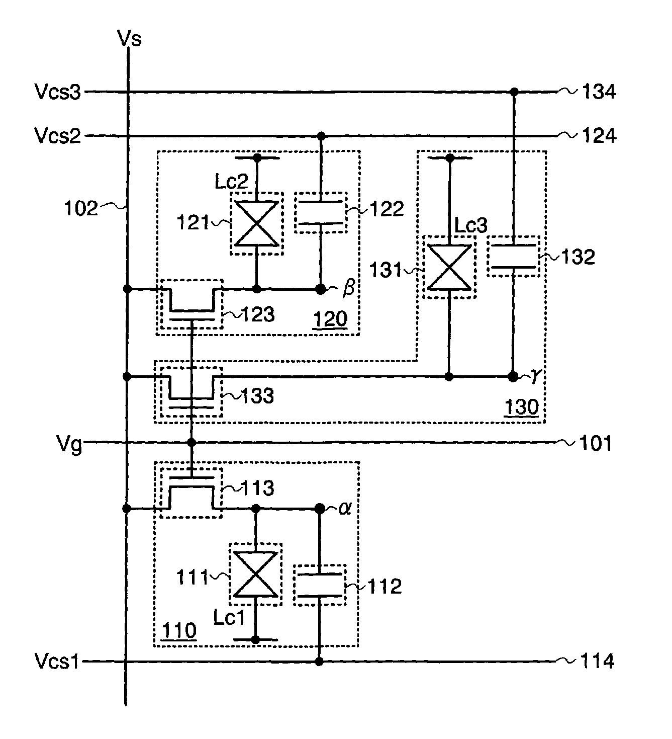
A liquid crystal display device of the present invention includes a pixel having a first sub-pixel, a second sub-pixel, and a third sub-pixel, a scanning line, a signal line, a first capacitor wiring, a second capacitor wiring, and a third capacitor wiring. The first sub-pixel includes a first pixel electrode, a first transistor, and a first capacitor element. A gate of the first transistor is electrically connected to the scanning line, one of source and drain of the first transistor is electrically connected to the signal line, and the other of source and drain of the first transistor is electrically connected to the first pixel electrode. A first electrode of the first capacitor element is electrically connected to the first capacitor wiring, and a second electrode of the first capacitor element is electrically connected to the first pixel electrode. The second sub-pixel includes a second pixel electrode, a second transistor, and a second capacitor element. A gate of the second transistor is electrically connected to the scanning line, one of source and drain of the second transistor is electrically connected to the signal line, and the other of source and drain of the second transistor is electrically connected to the second pixel electrode. A first electrode of the second capacitor element is electrically connected to the second capacitor wiring, and a second electrode of the second capacitor element is electrically connected to the second pixel electrode. The third sub-pixel includes a third pixel electrode, a third transistor, and a third capacitor element. A gate of the third transistor is electrically connected to the scanning line, one of source and drain of the third transistor is electrically connected to the signal line, and the other of source and drain of the third transistor is electrically connected to the third pixel electrode. A first electrode of the third capacitor element is electrically connected to the third capacitor wiring, and a second electrode of the third capacitor element is electrically connected to the third pixel electrode. Potentials of the first capacitor wiring and the second capacitor wiring vary, and a potential of the third capacitor wiring is almost constant. Note that, the case where the potential of the third capacitor wiring is almost constant includes, during a period when a potential is applied to the third capacitor wiring, the case where the potential of the third capacitor wiring is not constant in part of the period as well as the case where the potential of the third capacitor element is always constant. In addition, percentage of "part of the period" is preferably 10% or less of the period during which a potential is applied to the third capacitor wiring, or more preferably, 1% or less. In addition, the case where the potential of the third capacitor wiring fluctuates and changes because of noise and the like may be included in the case where the potential of the third capacitor wiring is almost constant.
A liquid crystal display device of the present invention includes a pixel having a first sub-pixel, a second sub-pixel, and a third sub-pixel, a plurality of scanning lines including a first scanning line, a signal line, a first capacitor wiring, and a second capacitor wiring. The first sub-pixel includes a first pixel electrode, a first transistor, and a first capacitor element. A gate of the first transistor is electrically connected to the first scanning line, one of source and drain of the first transistor is electrically connected to the signal line, and the other of source and drain of the first transistor is electrically connected to the first pixel electrode. A first electrode of the first capacitor element is electrically connected to the first capacitor wiring, and a second electrode of the first capacitor element is electrically connected to the first pixel electrode. The second sub-pixel includes a second pixel electrode, a second transistor, and a second capacitor element. A gate of the second transistor is electrically connected to the first scanning line, one of source and drain of the second transistor is electrically connected to the signal line, and the other of source and drain of the second transistor is electrically connected to the second pixel electrode. A first electrode of the second capacitor element is electrically connected to the second capacitor wiring, and a second electrode of the second capacitor element is electrically connected to the second pixel electrode. The third sub-pixel includes a third pixel electrode, a third transistor, and a third capacitor element. A gate of the third transistor is electrically connected to the first scanning line, one of source and drain of the third transistor is electrically connected to the signal line, and the other of source and drain of the third transistor is electrically connected to the third pixel electrode. A first electrode of the third capacitor element is electrically connected to a second scanning line which is different from the first scanning line, and a second electrode of the third capacitor element is electrically connected to the third pixel electrode. Potentials of the first capacitor wiring and the second capacitor wiring vary.
A liquid crystal display device of the present invention includes a pixel having a first sub-pixel, a second sub-pixel, a third sub-pixel, and a fourth sub-pixel, a scanning line, a signal line, a first capacitor wiring, a second capacitor wiring, a third capacitor wiring, and a fourth capacitor wiring. The first sub-pixel includes a first pixel electrode, a first transistor, and a first capacitor element. A gate of the first transistor is electrically connected to the scanning line, one of source and drain of the first transistor is electrically connected to the signal line, and the other of source and drain of the first transistor is electrically connected to the first pixel electrode. A first electrode of the first capacitor element is electrically connected to the first capacitor wiring, a second electrode of the first capacitor element is electrically connected to the first pixel electrode. The second sub-pixel includes a second pixel electrode, a second transistor, and a second capacitor element. A gate of the second transistor is electrically connected to the scanning line, one of source and drain of the second transistor is electrically connected to the signal line, and the other of source and drain of the second transistor is electrically connected to the second pixel electrode. A first electrode of the second capacitor element is electrically connected to the second capacitor wiring, and a second electrode of the second capacitor element is electrically connected to the second pixel electrode. The third sub-pixel includes a third pixel electrode, a third transistor, and a third capacitor element. A gate of the third transistor is electrically connected to the scanning line, one of source and drain of the third transistor is electrically connected to the signal line, and the other of source and drain of the third transistor is electrically connected to the third pixel electrode. A first electrode of the third capacitor element is electrically connected to the third capacitor wiring, a second electrode of the third capacitor element is electrically connected to the third pixel electrode. The fourth sub-pixel includes a fourth pixel electrode, a fourth transistor, and a fourth capacitor element. A gate of the fourth transistor is electrically connected to the scanning line, one of source and drain of the fourth transistor is electrically connected to the signal line, and the other of source and drain of the fourth transistor is electrically connected to the fourth pixel electrode. A first electrode of the fourth capacitor element is electrically connected to the fourth capacitor wiring, and a second electrode of the fourth capacitor element is electrically connected to the fourth pixel electrode. Potentials of the first capacitor wiring and the second capacitor wiring vary, and potentials of the third capacitor wiring and the fourth capacitor wiring are almost constant.
Note that as the display device of the present invention, an active matrix display device such as a liquid crystal display device, a light-emitting device provided with a light-emitting element typified by an organic light-emitting element (OLED) in each pixel, a DMD (digital micromirror device), a PDP (plasma display panel), or an FED (field emission display) is included in its category. In addition, a passive matrix display device is also included therein.
Note that various types of switches can be used as a switch. An electrical switch, a mechanical switch, and the like are given as examples. That is, any element can be used as long as it can control a current flow, without limiting to a certain element. For example, a transistor (e.g., a bipolar transistor or a MOS transistor), a diode (e.g., a PN diode, a PIN diode, a Schottky diode, an MIM (metal insulator metal) diode, an MIS (metal insulator semiconductor) diode, or a diode-connected transistor), a thyristor, or the like can be used as a switch. Alternatively, a logic circuit combining such elements can be used as a switch.
An example of a mechanical switch is a switch formed using MEMS (micro electro mechanical system) technology, such as a digital micromirror device (DMD). Such a switch includes an electrode which can be moved mechanically, and operates by controlling connection and non-connection based on movement of the electrode.
In the case of using a transistor as a switch, polarity (a conductivity type) of the transistor is not particularly limited because it operates just as a switch. However, a transistor of polarity with smaller off-current is preferably used when off-current is to be suppressed. Examples of a transistor with smaller off-current are a transistor provided with an LDD region, a transistor with a multi-gate structure, and the like. In addition, it is preferable that an N-channel transistor be used when a potential of a source terminal is closer to a potential of a low-potential-side power supply (e.g., V.sub.ss, GND, or 0 V), while a P-channel transistor be used when the potential of the source terminal is closer to a potential of a high-potential-side power supply (e.g., V.sub.dd). This is because the absolute value of gate-source voltage can be increased when the potential of the source terminal is closer to a potential of a low-potential-side power supply in an N-channel transistor and when the potential of the source terminal is closer to a potential of a high-potential-side power supply in a P-channel transistor so that the transistor easily operates as a switch. This is also because the transistor does not often perform a source follower operation, so that reduction in output voltage does not often occur.
Note that a CMOS switch may be employed as a switch by using both N-channel and P-channel transistors. When a CMOS switch is employed, the switch can more precisely operate as a switch because current can flow when either the P-channel transistor or the N-channel transistor is turned on. For example, voltage can be appropriately output regardless of whether voltage of an input signal to the switch is high or low. In addition, since a voltage amplitude value of a signal for turning on or off the switch can be made small, power consumption can be reduced.
Note that when a transistor is used as a switch, the switch includes an input terminal (one of a source terminal and a drain terminal), an output terminal (the other of the source terminal and the drain terminal), and a terminal (a gate terminal) for controlling electric conduction. On the other hand, when a diode is used as a switch, the switch does not have a terminal for controlling electric conduction in some cases. Therefore, when a diode is used as a switch, the number of wirings for controlling terminals can be further reduced than the case of using a transistor as a switch.
Note that when it is explicitly described that "A and B are connected", the case where A and B are electrically connected, the case where A and B are functionally connected, and the case where A and B are directly connected are included therein. Here, each of A and B corresponds to an object (e.g., a device, an element, a circuit, a wiring, an electrode, a terminal, a conductive film, or a layer). Accordingly, another element may be interposed between elements having a connection relation shown in drawings and texts, without limiting to a predetermined connection relation, for example, the connection relation shown in the drawings and the texts.
For example, in the case where A and B are electrically connected, one or more elements which enable electric connection between A and B (e.g., a switch, a transistor, a capacitor, an inductor, a resistor, and/or a diode) may be provided between A and B. In addition, in the case where A and B are functionally connected, one or more circuits which enable functional connection between A and B (e.g., a logic circuit such as an inverter, a NAND circuit, or a NOR circuit, a signal converter circuit such as a DA converter circuit, an AD converter circuit, or a gamma correction circuit, a potential level converter circuit such as a power supply circuit (e.g., a pressure rising circuit, or a pressure lowing circuit) or a level shifter circuit for changing a potential level of a signal, a voltage source, a current source, a switching circuit, or an amplifier circuit such as a circuit which can increase signal amplitude, the amount of current, or the like (e.g., an operational amplifier, a differential amplifier circuit, a source follower circuit, or a buffer circuit), a signal generating circuit, a memory circuit, and/or a control circuit) may be provided between A and B. Alternatively, in the case where A and B are directly connected, A and B may be directly connected without interposing another element or another circuit therebetween.
Note that when it is explicitly described that "A and B are directly connected", the case where A and B are directly connected (i.e., the case where A and B are connected without interposing another element or another circuit therebetween) and the case where A and B are electrically connected (i.e., the case where A and B are connected by interposing another element or another circuit therebetween) are included therein.
Note that when it is explicitly described that "A and B are electrically connected", the case where A and B are electrically connected (i.e., the case where A and B are connected by interposing another element or another circuit therebetween), the case where A and B are functionally connected (i.e., the case where A and B are functionally connected by interposing another circuit therebetween), and the case where A and B are directly connected (i.e., the case where A and B are connected without interposing another element or another circuit therebetween) are included therein. That is, when it is explicitly described that "A and B are electrically connected", the description is the same as the case where it is explicitly only described that "A and B are connected".
Note that a display element, a display device which is a device having a display element, a light-emitting element, and a light-emitting device which is a device having a light-emitting element can use various modes and can include various elements. For example, as a display element, a display device, a light-emitting element, or a light-emitting device, a display medium whose contrast, luminance, reflectivity, transmittivity, or the like is changed by an electromagnetic action can be employed; an EL element (e.g., an EL element including organic and inorganic materials, an organic EL element, or an inorganic EL element), an electron emitter, a liquid crystal element, electronic ink, an electrophoresis element, a grating light valve (GLV), a plasma display panel (PDP), a digital micromirror device (DMD), a piezoelectric ceramic display, a carbon nanotube, or the like can be used. Note that display devices using EL elements include an EL display; display devices using electron emitters include a field emission display (FED), an SED-type flat panel display (SED: surface-conduction electron-emitter display), and the like; display devices using liquid crystal elements include a liquid crystal display (e.g., a transmissive liquid crystal display, a transflective liquid crystal display, a reflective liquid crystal display, a direct-view liquid crystal display, or a projection liquid crystal display); and display devices using electronic ink or electrophoresis elements include an electronic paper.
Note that an EL element is an element having an anode, a cathode, and an EL layer interposed between the anode and the cathode. Note that as an EL layer, a layer utilizing light emission (fluorescence) from a singlet exciton, a layer utilizing light emission (phosphorescence) from a triplet exciton, a layer utilizing light emission (fluorescence) from a singlet exciton and light emission (phosphorescence) from a triplet exciton, a layer formed of an organic material, a layer formed of an inorganic material, a layer formed of an organic material and an inorganic material, a layer including a high-molecular material, a layer including a low molecular material, a layer including a low-molecular material and a high-molecular material, or the like can be used. Note that the present invention is not limited to this, and various EL elements can be used as an EL element.
Note that an electron emitter is an element in which electrons are extracted by high electric field concentration on a pointed cathode. For example, as an electron emitter, a Spindt type, a carbon nanotube (CNT) type, a metal-insulator-metal (MIM) type in which a metal, an insulator, and a metal are stacked, a metal-insulator-semiconductor (MIS) type in which a metal, an insulator, and a semiconductor are stacked, a MOS type, a silicon type, a thin film diode type, a diamond type, a surface conduction emitter SCD type, a thin film type in which a metal, an insulator, a semiconductor, and a metal are stacked and the like, an HEED type, an EL type, a porous silicon type, a surface-conduction (SED) type, or the like can be used. However, the present invention is not limited to this, and various elements can be used as an electron emitter.
Note that a liquid crystal element is an element which controls transmission or non-transmission of light by optical modulation action of a liquid crystal and includes a pair of electrodes and a liquid crystal. Note that optical modulation action of a liquid crystal is controlled by an electric filed applied to the liquid crystal (including a horizontal electric field, a vertical electric field, and an oblique electric field). Note that the following can be used for a liquid crystal element: a nematic liquid crystal, a cholesteric liquid crystal, a smectic liquid crystal, a discotic liquid crystal, a thermotropic liquid crystal, a lyotropic liquid crystal, a low-molecular liquid crystal, a high-molecular liquid crystal, a ferroelectric liquid crystal, an anti-ferroelectric liquid crystal, a main-chain liquid crystal, a side-chain high-molecular liquid crystal, a plasma addressed liquid crystal (PALC), a banana-shaped liquid crystal, and the like. In addition, the following can be used as a driving method of a liquid crystal: a TN (twisted nematic) mode, an STN (super twisted nematic) mode, an IPS (in-plane-switching) mode, an FFS (fringe field switching) mode, an MVA (multi-domain vertical alignment) mode, a PVA (patterned vertical alignment) mode, an ASV (advanced super view) mode, an ASM (axially symmetric aligned micro-cell) mode, an OCB (optical compensated birefringence) mode, an ECB (electrically controlled birefringence) mode, an FLC (ferroelectric liquid crystal) mode, an AFLC (anti-ferroelectric liquid crystal) mode, a PDLC (polymer dispersed liquid crystal) mode, a guest-host mode, and the like. Note that the present invention is not limited to this, and various liquid crystal elements and driving methods can be used as a liquid crystal element and a driving method thereof.
Note that electronic paper corresponds to a device which displays an image by molecules which utilize optical anisotropy, dye molecular orientation, or the like; a device which displays an image by particles which utilize electrophoresis, particle movement, particle rotation, phase change, or the like; a device which displays an image by moving one end of a film; a device which displays an image by using light emission or phase change of molecules; a device which displays an image by using optical absorption by molecules; and a device which displays an image by using self-light emission by bonding electrons and holes. For example, the following can be used for a display method of electronic paper: microcapsule electrophoresis, horizontal electrophoresis, vertical electrophoresis, a spherical twisting ball, a magnetic twisting ball, a columnar twisting ball, a charged toner, electro liquid powder, magnetic electrophoresis, a magnetic thermosensitive type, an electrowetting type, a light-scattering (transparent-opaque change) type, a cholesteric liquid crystal and a photoconductive layer, a cholesteric liquid crystal device, a bistable nematic liquid crystal, a ferroelectric liquid crystal, a liquid crystal dispersed type with a dichroic dye, a movable film, coloring and decoloring properties of a leuco dye, a photochromic material, an electrochromic material, an electrodeposition material, flexible organic EL, and the like. Note that the present invention is not limited to this, and various electronic paper and display methods can be used as electronic paper and a display method thereof. Here, when microcapsule electrophoresis is used, defects of electrophoresis, which are aggregation and precipitation of phoresis particles, can be solved. Electro liquid powder has advantages such as high-speed response, high reflectivity, wide viewing angle, low power consumption, and memory properties.
Note that a plasma display panel has a structure in which a substrate having a surface provided with an electrode and a substrate having a surface provided with an electrode and a minute groove in which a phosphor layer is formed face each other at a narrow interval and a rare gas is sealed therein. Note that display can be performed by applying voltage between the electrodes to generate an ultraviolet ray so that a phosphor emits light. Note that the plasma display panel may be a DC-type PDP or an AC-type PDP. As a driving method of the plasma display panel, AWS (address while sustain) driving, ADS (address display separated) driving in which a subframe is divided into a reset period, an address period, and a sustain period, CLEAR (high-contrast, low energy address and reduction of false contour sequence) driving, ALIS (alternate lighting of surfaces) method, TERES (technology of reciprocal sustainer) driving, or the like can be used. Note that the present invention is not limited to this, and various driving methods can be used as a driving method of a plasma display panel.
Note that electroluminescence, a cold cathode fluorescent lamp, a hot cathode fluorescent lamp, an LED, a laser light source, a mercury lamp, or the like can be used as a light source of a display device in which a light source is necessary, such as a liquid crystal display (a transmissive liquid crystal display, a transflective liquid crystal display, a reflective liquid crystal display, a direct-view liquid crystal display, or a projection liquid crystal display), a display device using a grating light valve (GLV), or a display device using a digital micromirror device (DMD). Note that the present invention is not limited to this, and various light sources can be used as a light source.
Note that various types of transistors can be used as a transistor, without limiting to a certain type. For example, a thin film transistor (TFT) including a non-single crystal semiconductor film typified by amorphous silicon, polycrystalline silicon, microcrystalline (also referred to as semi-amorphous) silicon, or the like can be used. In the case of using the TFT, there are various advantages. For example, since the TFT can be formed at temperature lower than that of the case of using single-crystal silicon, manufacturing cost can be reduced or a manufacturing apparatus can be made larger. Since the manufacturing apparatus is made larger, the TFT can be formed using a large substrate. Therefore, many display devices can be formed at the same time at low cost. In addition, a substrate having low heat resistance can be used because of low manufacturing temperature. Therefore, the transistor can be formed using a transparent substrate. Accordingly, transmission of light in a display element can be controlled by using the transistor formed using the transparent substrate. Alternatively, part of a film which forms the transistor can transmit light because the film thickness of the transistor is thin. Therefore, the aperture ratio can be improved.
Note that when a catalyst (e.g., nickel) is used in the ease of forming polycrystalline silicon, crystallinity can be further improved and a transistor having excellent electric characteristics can be formed. Accordingly, a gate driver circuit (e.g., a scanning line driver circuit), a source driver circuit (e.g., a signal line driver circuit), and/or a signal processing circuit (e.g., a signal generation circuit, a gamma correction circuit, or a DA converter circuit) can be formed over the same substrate as a pixel portion.
Note that when a catalyst (e.g., nickel) is used in the case of forming microcrystalline silicon, crystallinity can be further improved and a transistor having excellent electric characteristics can be formed. At this time, crystallinity can be improved by just performing heat treatment without performing laser irradiation. Accordingly, a gate driver circuit (e.g., a scanning line driver circuit) and part of a source driver circuit (e.g., an analog switch) can be formed over the same substrate. In addition, in the case of not performing laser irradiation for crystallization, crystallinity unevenness of silicon can be suppressed. Therefore, a high-quality image can be displayed.
Note that polycrystalline silicon and microcrystalline silicon can be formed without using a catalyst (e.g., nickel).
Note that it is preferable that crystallinity of silicon be improved to polycrystal, microcrystal, or the like in the whole panel; however, the present invention is not limited to this. Crystallinity of silicon may be improved only in part of the panel. Selective increase in crystallinity can be achieved by selective laser irradiation or the like. For example, only a peripheral driver circuit region excluding pixels may be irradiated with laser light. Alternatively, only a region of a gate driver circuit, a source driver circuit, or the like may be irradiated with laser light. Further alternatively, only part of a source driver circuit (e.g., an analog switch) may be irradiated with laser light. Accordingly, crystallinity of silicon can be improved only in a region in which a circuit needs to be operated at high speed. Since a pixel region is not necessarily operated at high speed, even if crystallinity is not improved, the pixel circuit can be operated without problems. Since a region, crystallinity of which is improved, is small, manufacturing time can be decreased, throughput can be increased, and manufacturing cost can be reduced. Since the number of necessary manufacturing apparatus is small, manufacturing cost can be reduced.
A transistor can be formed by using a semiconductor substrate, an SOI substrate, or the like. Thus, a transistor with few variations in characteristics, sizes, shapes, or the like, with high current supply capacity, and with a small size can be formed. When such a transistor is used, power consumption of a circuit can be reduced or a circuit can be highly integrated.
A transistor including a compound semiconductor or an oxide semiconductor such as ZnO, a-InGaZnO, SiGe, GaAs, IZO, ITO, or SnO, a thin film transistor obtained by thinning such a compound semiconductor or a oxide semiconductor, or the like can be used. Thus, manufacturing temperature can be lowered and for example, such a transistor can be formed at room temperature. Accordingly, the transistor can be formed directly on a substrate having low heat resistance, such as a plastic substrate or a film substrate. Note that such a compound semiconductor or an oxide semiconductor can be used for not only a channel portion of the transistor but also other applications. For example, such a compound semiconductor or an oxide semiconductor can be used as a resistor, a pixel electrode, or a transparent electrode. Further, since such an element can be formed at the same time as the transistor, cost can be reduced.
A transistor formed by using an inkjet method or a printing method, or the like can be used. Accordingly, a transistor can be formed at room temperature, can be formed at a low vacuum, or can be formed using a large substrate. In addition, since the transistor can be formed without using a mask (a reticle), a layout of the transistor can be easily changed. Further, since it is not necessary to use a resist, material cost is reduced and the number of steps can be reduced. Furthermore, since a film is formed only in a necessary portion, a material is not wasted compared with a manufacturing method in which etching is performed after the film is formed over the entire surface, so that cost can be reduced.
A transistor including an organic semiconductor or a carbon nanotube, or the like can be used. Accordingly, such a transistor can be formed using a substrate which can be bent. Therefore, a device using a transistor including an organic semiconductor or a carbon nanotube, or the like can resist a shock.
Further, transistors with various structures can be used. For example, a MOS transistor, a junction transistor, a bipolar transistor, or the like can be used as a transistor. When a MOS transistor is used, the size of the transistor can be reduced. Thus, a large number of transistors can be mounted. When a bipolar transistor is used, large current can flow. Thus, a circuit can be operated at high speed.
Note that a MOS transistor, a bipolar transistor, and the like may be formed over one substrate. Thus, reduction in power consumption, reduction in size, high speed operation, and the like can be realized.
Furthermore, various transistors can be used.
Note that a transistor can be formed using various types of substrates without limiting to a certain type. For example, as a substrate over which a transistor is formed, a single-crystaline substrate, an SOI substrate, a glass substrate, a quartz substrate, a plastic substrate, a paper substrate, a cellophane substrate, a stone substrate, a wood substrate, a cloth substrate (including a natural fiber (e.g., silk, cotton, or hemp), a synthetic fiber (e.g., nylon, polyurethane, or polyester), a regenerated fiber (e.g., acetate, cupra, rayon, or regenerated polyester), or the like), a leather substrate, a rubber substrate, a stainless steel substrate, a substrate including a stainless steel foil, or the like can be used as a substrate. Alternatively, a skin (e.g., epidermis or corium) or hypodermal tissue of an animal such as a human being can be used as a substrate. Further alternatively, the transistor may be formed using one substrate, and then, the transistor may be transferred to another substrate. A single-crystalline substrate, an SOI substrate, a glass substrate, a quartz substrate, a plastic substrate, a paper substrate, a cellophane substrate, a stone substrate, a wood substrate, a cloth substrate (including a natural fiber (e.g., silk, cotton, or hemp), a synthetic fiber (e.g., nylon, polyurethane, or polyester), a regenerated fiber (e.g., acetate, cupra, rayon, or regenerated polyester), or the like), a leather substrate, a rubber substrate, a stainless steel substrate, a substrate including a stainless steel foil, or the like can be used as a substrate to which the transistor is transferred. Alternatively, a skin (e.g., epidermis or corium) or hypodermal tissue of an animal such as a human being can be used as a substrate to which the transistor is transferred. Further alternatively, the transistor may be formed using one substrate and the substrate may be thinned by polishing. A single-crystalline substrate, an SOI substrate, a glass substrate, a quartz substrate, a plastic substrate, a paper substrate, a cellophane substrate, a stone substrate, a wood substrate, a cloth substrate (including a natural fiber (e.g., silk, cotton, or hemp), a synthetic fiber (e.g., nylon, polyurethane, or polyester), a regenerated fiber (e.g., acetate, cupra, rayon, or regenerated polyester), or the like), a leather substrate, a rubber substrate, a stainless steel substrate, a substrate including a stainless steel foil, or the like can be used as the substrate to be polished. Alternatively, a skin (e.g., epidermis or corium) or hypodermal tissue of an animal such as a human being can be used as the substrate to be polished. When such a substrate is used, a transistor with excellent properties or a transistor with low power consumption can be formed, a device with high durability, high heat resistance can be provided, or reduction in weight or thickness can be achieved.
Note that a structure of a transistor can be various modes without limiting to a certain structure. For example, a multi-gate structure having two or more gate electrodes may be used. When the multi-gate structure is used, a structure where a plurality of transistors are connected in series is provided because channel regions are connected in series. With the multi-gate structure, off-current can be reduced or the withstand voltage of the transistor can be increased to improve reliability. Alternatively, with the multi-gate structure, drain-source current does not fluctuate very much even if drain-source voltage fluctuates when the transistor operates in a saturation region, so that a flat slope of voltage-current characteristics can be obtained. When the flat slope of the voltage-current characteristics is utilized, an ideal current source circuit or an active load having an extremely high resistance value can be realized. Accordingly, a differential circuit or a current mirror circuit having excellent properties can be realized. Alternatively, a structure where gate electrodes are formed above and below a channel may be used. When the structure where gate electrodes are formed above and below the channel is used, a channel region is increased, so that the amount of current flowing therethrough can be increased or a depletion layer can be easily formed to decrease subthreshold swing. When the gate electrodes are formed above and below the channel, a structure where a plurality of transistors are connected in parallel may be provided.
Alternatively, a structure where a gate electrode is formed above a channel region, a structure where a gate electrode is formed below a channel region, a staggered structure, an inversely staggered structure, a structure where a channel region is divided into a plurality of regions, or a structure where channel regions are connected in parallel or in series can be used. Further alternatively, a source electrode or a drain electrode may overlap with a channel region (or part of it). When the structure where the source electrode or the drain electrode may overlap with the channel region (or part of it) is used, the case can be prevented in which electric charges are accumulated in part of the channel region, which would result in an unstable operation. Further alternatively, an LDD region may be provided. When the LDD region is provided, off-current can be reduced or the withstand voltage of the transistor can be increased to improve reliability. Further, when the LDD region is provided, drain-source current does not fluctuate very much even if drain-source voltage fluctuates when the transistor operates in the saturation region, so that a flat slope of voltage-current characteristics can be obtained.
Note that various types of transistors can be used as a transistor and the transistor can be formed using various types of substrates. Accordingly, all the circuits that are necessary to realize a predetermined function may be formed using the same substrate. For example, all the circuits that are necessary to realize the predetermined function may be formed using a glass substrate, a plastic substrate, a single-crystalline substrate, an SOI substrate, or any other substrate. When all the circuits that are necessary to realize the predetermined function are formed using the same substrate, cost can be reduced by reduction in the number of component parts or reliability can be improved by reduction in the number of connections to circuit components. Alternatively, part of the circuits which are necessary to realize the predetermined function may be formed using one substrate and another part of the circuits which are necessary to realize the predetermined function may be formed using another substrate. That is, not all the circuits that are necessary to realize the predetermined function are required to be formed using the same substrate. For example, part of the circuits which are necessary to realize the predetermined function may be formed by transistors formed over a glass substrate and another part of the circuits which are necessary to realize the predetermined function may be formed over a single-crystal semiconductor substrate, so that an IC chip formed by a transistor formed over the single-crystalline substrate may be connected to the glass substrate by COG (chip on glass) and the IC chip may be provided over the glass substrate. Alternatively, the IC chip may be connected to the glass substrate by TAB (tape automated bonding) or a printed wiring board. When part of the circuits are formed using the same substrate in this manner, cost can be reduced by reduction in the number of component parts or reliability can be improved by reduction in the number of connections to circuit components. Further alternatively, when circuits with high driving voltage and high driving frequency, which consume large power, are formed over a single-crystalline substrate instead of forming such circuits using the same substrate and an IC chip formed by the circuit is used, increase in power consumption can be prevented.
Note that one pixel corresponds to one element whose brightness can be controlled. Therefore, for example, one pixel corresponds to one color element and brightness is expressed with the one color element. Accordingly, in the case of a color display device having color elements of R (red), G (green), and B (blue), a minimum unit of an image is formed of three pixels of an R pixel, a G pixel, and a B pixel. Note that the color elements are not limited to three colors, and color elements of more than three colors may be used or a color other than RGB may be used. For example, RGBW (W corresponds to white) may be used by adding white. Alternatively, one or more colors of yellow, cyan, magenta emerald green, vermilion, and the like may be added to RGB. Further alternatively, a color similar to at least one of R, G, and B may be added to RGB. For example, R, G, B1, and B2 may be used. Although both B1 and B2 are blue, they have slightly different frequency. Similarly, R1, R2, G, and B may be used. When such color elements are used, display which is closer to the real object can be performed and power consumption can be reduced. As another example, in the case of controlling brightness of one color element by using a plurality of regions, one region may correspond to one pixel. Therefore, for example, in the case of performing area ratio gray scale display or the case of including a subpixel, a plurality of regions which control brightness are provided in each color element and gray scales are expressed with the whole regions. In this case, one region which controls brightness may correspond to one pixel. Thus, in that case, one color element includes a plurality of pixels. Alternatively, even when the plurality of regions which control brightness are provided in one color element, these regions may be collected as one pixel. Thus, in that case, one color element includes one pixel. Further alternatively, in the case where brightness is controlled in a plurality of regions in each color element, regions which contribute to display have different area dimensions depending on pixels in some cases. Further alternatively, in the plurality of regions which control brightness in each color element, signals supplied to each of the plurality of regions may be slightly varied to widen a viewing angle. That is, potentials of pixel electrodes included in the plurality of regions provided in each color element may be different from each other. Accordingly, voltage applied to liquid crystal molecules are varied depending on the pixel electrodes. Therefore, the viewing angle can be widened.
Note that explicit description "one pixel (for three colors)" corresponds to the case where three pixels of R, Q, and B are considered as one pixel. Meanwhile, explicit description "one pixel (for one color)" corresponds to the case where the plurality of regions are provided in each color element and collectively considered as one pixel.
Note that in this document (a specification, claims, drawings, and the like), pixels are provided (arranged) in matrix in some cases. Here, description that pixels are provided (arranged) in matrix includes the case where the pixels are arranged in a straight line and the case where the pixels are arranged in a jagged line, in a longitudinal direction or a lateral direction. Thus, for example, in the case of performing full color display with three color elements (e.g., RGB), the following cases are included therein: the case where the pixels are arranged in stripes and the case where dots of the three color elements are arranged in a delta pattern. In addition, the case is also included therein in which dots of the three color elements are provided in Bayer arrangement. Note that the color elements are not limited to three colors, and color elements of more than three colors may be used. For example, RGBW (W corresponds to white), RGB plus one or more of yellow, cyan, magenta, and the like, or the like may be used. Further, the sizes of display regions may be different between respective dots of color elements. Thus, power consumption can be reduced or the life of a display element can be prolonged.
Note that an active matrix method in which an active element is included in a pixel or a passive matrix method in which an active element is not included in a pixel can be used.
In an active matrix method, as an active element (a non-linear element), not only a transistor but also various active elements (non-linear elements) can be used. For example, an MIM (metal insulator metal), a TF) (thin film diode), or the like can also be used. Since such an element has few number of manufacturing steps, manufacturing cost can be reduced or yield can be improved. Further, since the size of the element is small, the aperture ratio can be improved, so that power consumption can be reduced or high luminance can be achieved.
Note that as a method other than an active matrix method, a passive matrix method in which an active element (a non-linear element) is not used can also be used. Since an active element (a non-linear element) is not used, manufacturing steps is few, so that manufacturing cost can be reduced or the yield can be improved. Further, since an active element (a non-linear element) is not used, the aperture ratio can be improved, so that power consumption can be reduced or high luminance can be achieved.
Note that a transistor is an element having at least three terminals of a gate, a drain, and a source. The transistor has a channel region between a drain region and a source region, and current can flow through the drain region, the channel region, and the source region. Here, since the source and the drain of the transistor change depending on the structure, the operating condition, and the like of the transistor, it is difficult to define which is a source or a drain. Therefore, in this document, a region functioning as a source and a drain may not be called the source or the drain. In such a case, one of the source and the drain may be referred to as a first terminal and the other thereof may be referred to as a second terminal, for example. Alternatively, one of the source and the drain may be referred to as a first electrode and the other thereof may be referred to as a second electrode. Further alternatively, one of the source and the drain may be referred to as a source region and the other thereof may be called a drain region.
Note that a transistor may be an element having at least three terminals of a base, an emitter, and a collector. In this case, one of the emitter and the collector may be similarly referred to as a first terminal and the other terminal may be referred to as a second terminal.
Note that a gate corresponds to all or part of a gate electrode and a gate wiring (also referred to as a gate line, a gate signal line, a scanning line, a scan signal line, or the like). A gate electrode corresponds to a conductive film which overlaps with a semiconductor which forms a channel region with a gate insulating film interposed therebetween. Note that part of the gate electrode overlaps with an LDD (lightly doped drain) region or the source region (or the drain region) with the gate insulating film interposed therebetween in some cases. A gate wiring corresponds to a wiring for connecting a gate electrode of each transistor to each other, a wiring for connecting a gate electrode of each pixel to each other, or a wiring for connecting a gate electrode to another wiring.
However, there is a portion (a region, a conductive film, a wiring, or the like) which functions as both a gate electrode and a gate wiring. Such a portion (a region, a conductive film, a wiring, or the like) may be referred to as either a gate electrode or a gate wiring. That is, there is a region where a gate electrode and a gate wiring cannot be clearly distinguished from each other. For example, in the case where a channel region overlaps with part of an extended gate wiring, the overlapped portion (region, conductive film, wiring, or the like) functions as both a gate wiring and a gate electrode. Accordingly, such a portion (a region, a conductive film, a wiring, or the like) may be referred to as either a gate electrode or a gate wiring.
Note that a portion (a region, a conductive film, a wiring, or the like) which is formed using the same material as a gate electrode, forms the same island as the gate electrode, and is connected to the gate electrode may also be referred to as a gate electrode. Similarly, a portion (a region, a conductive film, a wiring, or the like) which is formed using the same material as a gate wiring, forms the same island as the gate wiring, and is connected to the gate wiring may also be referred to as a gate wiring. In a strict sense, such a portion (a region, a conductive film, a wiring, or the like) does not overlap with a channel region or does not have a function of connecting the gate electrode to another gate electrode in some cases. However, there is a portion (a region, a conductive film, a wiring, or the like) which is formed using the same material as a gate electrode or a gate wiring, forms the same island as the gate electrode or the gate wiring, and is connected to the gate electrode or the gate wiring because of specifications or the like in manufacturing. Thus, such a portion (a region, a conductive film, a wiring, or the like) may also be referred to as either a gate electrode or a gate wiring.
Note that in a multi-gate transistor, for example, a gate electrode is often connected to another gate electrode by using a conductive film which is formed using the same material as the gate electrode. Since such a portion (a region, a conductive film, a wiring, or the like) is a portion (a region, a conductive film, a wiring, or the like) for connecting the gate electrode to another gate electrode, it may be referred to as a gate wiring, and it may also be referred to as a gate electrode because a multi-gate transistor can be considered as one transistor. That is, a portion (a region, a conductive film, a wiring, or the like) which is formed using the same material as a gate electrode or a gate wiring, forms the same island as the gate electrode or the gate wiring, and is connected to the gate electrode or the gate wiring may be referred to as either a gate electrode or a gate wiring. In addition, for example, part of a conductive film which connects the gate electrode and the gate wiring and is formed using a material which is different from that of the gate electrode or the gate wiring may also be referred to as either a gate electrode or a gate wiring.
Note that a gate terminal corresponds to part of a portion (a region, a conductive film, a wiring, or the like) of a gate electrode or a portion (a region, a conductive film, a wiring, or the like) which is electrically connected to the gate electrode.
Note that when a wiring is referred to as a gate wiring, a gate line, a gate signal line, a scanning line, a scan signal line, there is the case in which a gate of a transistor is not connected to a wiring. In this case, the gate wiring, the gate line, the gate signal line, the scanning line, or the scan signal line corresponds to a wiring formed in the same layer as the gate of the transistor, a wiring formed using the same material of the gate of the transistor, or a wiring formed at the same time as the gate of the transistor in some cases. As examples, there are a wiring for storage capacitance, a power supply line, a reference potential supply line, and the like.
Note that a source corresponds to all or part of a source region, a source electrode, and a source wiring (also referred to as a source line, a source signal line, a data line, a data signal line, or the like). A source region corresponds to a semiconductor region including a large amount of p-type impurities (e.g., boron or gallium) or n-type impurities (e.g., phosphorus or arsenic). Therefore, a region including a small amount of p-type impurities or n-type impurities, namely, an LDD (lightly doped drain) region is not included in the source region. A source electrode is part of a conductive layer which is formed using a material different from that of a source region and is electrically connected to the source region. However, there is the case where a source electrode and a source region are collectively referred to as a source electrode. A source wiring is a wiring for connecting a source electrode of each transistor to each other, a wiring for connecting a source electrode of each pixel to each other, or a wiring for connecting a source electrode to another wiring.
However, there is a portion (a region, a conductive film, a wiring, or the like) functioning as both a source electrode and a source wiring. Such a portion (a region, a conductive film, a wiring, or the like) may be referred to as either a source electrode or a source wiring. That is, there is a region where a source electrode and a source wiring cannot be clearly distinguished from each other. For example, in the case where a source region overlaps with part of an extended source wiring, the overlapped portion (region, conductive film, wiring, or the like) functions as both a source wiring and a source electrode. Accordingly, such a portion (a region, a conductive film, a wiring, or the like) may be referred to as either a source electrode or a source wiring.
Note that a portion (a region, a conductive film, a wiring, or the like) which is formed using the same material as a source electrode, forms the same island as the source electrode, and is connected to the source electrode, or a portion (a region, a conductive film, a wiring, or the like) which connects a source electrode and another source electrode may also be referred to as a source electrode. Further, a portion which overlaps with a source region may be referred to as a source electrode. Similarly, a portion (a region, a conductive film, a wiring, or the like) which is formed using the same material as a source wiring, forms the same island as the source wiring, and is connected to the source wiring may also be referred to as a source wiring. In a strict sense, such a portion (a region, a conductive film, a wiring, or the like) does not have a function of connecting the source electrode to another source electrode in some cases. However, there is a portion (a region, a conductive film, a wiring, or the like) which is formed using the same material as a source electrode or a source wiring, forms the same island as the source electrode or the source wiring, and is connected to the source electrode or the source wiring because of specifications or the like in manufacturing. Thus, such a portion (a region, a conductive film, a wiring, or the like) may also be referred to as either a source electrode or a source wiring.
For example, part of a conductive film which connects a source electrode and a source wiring and is formed using a material which is different from that of the source electrode or the source wiring may be referred to as either a source electrode or a source wiring.
Note that a source terminal corresponds to part of a source region, a source electrode, or a portion (a region, a conductive film, a wiring, or the like) which is electrically connected to the source electrode.
Note that when a wiring is referred to as a source wiring, a source line, a source signal line, a data line, a data signal line, there is the case in which a source (a drain) of a transistor is not connected to a wiring. In this case, the source wiring, the source line, the source signal line, the data line, or the data signal line corresponds to a wiring formed in the same layer as the source (the drain) of the transistor, a wiring formed using the same material of the source (the drain) of the transistor, or a wiring formed at the same time as the source (the drain) of the transistor in some cases. As examples, there are a wiring for storage capacitance, a power supply line, a reference potential supply line, and the like.
Note that the same can be said for a drain.
Note that a semiconductor device corresponds to a device having a circuit including a semiconductor element (e.g., a transistor, a diode, or a thyristor). The semiconductor device may also include all devices that can function by utilizing semiconductor characteristics. In addition, the semiconductor device corresponds to a device having a semiconductor material.
Note that a display element corresponds to an optical modulation element, a liquid crystal element, a light-emitting element, an EL element (an organic EL element, an inorganic EL element, or an EL element including organic and inorganic materials), an electron emitter, an electrophoresis element, a discharging element, a light-reflective element, a light diffraction element, a digital micromirfor device (DMD), or the like. Note that the present invention is not limited to this.
Note that a display device corresponds to a device having a display element. The display device may include a plurality of pixels each having a display element. Note that that the display device may also include a peripheral driver circuit for driving the plurality of pixels. The peripheral driver circuit for driving the plurality of pixels may be formed over the same substrate as the plurality of pixels. The display device may also include a peripheral driver circuit provided over a substrate by wire bonding or bump bonding, namely, an IC chip connected by chip on glass (COG) or an IC chip connected by TAB or the like. Further, the display device may also include a flexible printed circuit (FPC) to which an IC chip, a resistor, a capacitor, an inductor, a transistor, or the like is attached. Note also that the display device includes a printed wiring board (PWB) which is connected through a flexible printed circuit (FPC) and to which an IC chip, a resistor, a capacitor, an inductor, a transistor, or the like is attached. The display device may also include an optical sheet such as a polarizing plate or a retardation plate. The display device may also include a lighting device, a housing, an audio input and output device, a light sensor, or the like. Here, a lighting device such as a backlight unit may include a light guide plate, a prism sheet, a diffusion sheet, a reflective sheet, a light source (e.g., an LED or a cold cathode fluorescent lamp), a cooling device (e.g., a water cooling device or an air cooling device), or the like.
Note that a lighting device corresponds to a device having a backlight unit, a light guide plate, a prism sheet, a diffusion sheet, a reflective sheet, or a light source (e.g., an LED, a cold cathode fluorescent lamp, or a hot cathode fluorescent lamp), a cooling device, or the like.
Note that a light-emitting device corresponds to a device having a light-emitting element and the like. In the case of including a light-emitting element as a display element, the light-emitting device is one of specific examples of a display device.
Note that a reflective device corresponds to a device having a light-reflective element, a light diffraction element, light-reflective electrode, or the like.
Note that a liquid crystal display device corresponds to a display device including a liquid crystal element. Liquid crystal display devices include a direct-view liquid crystal display, a projection liquid crystal display, a transmissive liquid crystal display, a reflective liquid crystal display, a transflective liquid crystal display, and the like.
Note that a driving device corresponds to a device having a semiconductor element, an electric circuit, or an electronic circuit. For example, a transistor which controls input of a signal from a source signal line to a pixel (also referred to as a selection transistor, a switching transistor, or the like), a transistor which supplies voltage or current to a pixel electrode, a transistor which supplies voltage or current to a light-emitting element, and the like are examples of the driving device. A circuit which supplies a signal to a gate signal line (also referred to as a gate driver, a gate line driver circuit, or the like), a circuit which supplies a signal to a source signal line (also referred to as a source driver, a source line driver circuit, or the like) are also examples of the driving device.
Note that a display device, a semiconductor device, a lighting device, a cooling device, a light-emitting device, a reflective device, a driving device, and the like overlap with each other in some cases. For example, a display device includes a semiconductor device and a light-emitting device in some cases. Alternatively, a semiconductor device includes a display device and a driving device in some cases.
Note that when it is explicitly described that "B is formed on A" or "B is formed over A", it does not necessarily mean that B is formed in direct contact with A. The description includes the case where A and B are not in direct contact with each other, i.e., the case where another object is interposed between A and B. Here, each of A and B corresponds to an object (e.g., a device, an element, a circuit, a wiring, an electrode, a terminal, a conductive film, or a layer).
Accordingly, for example, when it is explicitly described that "a layer B is formed on (or over) a layer A", it includes both the case where the layer B is formed in direct contact with the layer A, and the case where another layer (e.g., a layer C or a layer D) is formed in direct contact with the layer A and the layer B is formed in direct contact with the layer C or D. Note that another layer (e.g., a layer C or a layer D) may be a single layer or a plurality of layers.
Similarly, when it is explicitly described that "B is formed above A", it does not necessarily mean that B is formed in direct contact with A, and another object may be interposed therebetween. Thus, for example, when it is described that "a layer B is formed above a layer A", it includes both the case where the layer B is formed in direct contact with the layer A, and the case where another layer (e.g., a layer C or a layer D) is formed in direct contact with the layer A and the layer B is formed in direct contact with the layer C or D. Note that another layer (e.g., a layer C or a layer D) may be a single layer or a plurality of layers.
Note that when it is explicitly described that "B is formed in direct contact with A", it includes not the case where another object is interposed between A and B but the case where B is formed in direct contact with A.
Note that the same can be said when it is described that B is formed below or under A.
Note that when an object is explicitly described in a singular form, the object is preferably singular. Note that the present invention is not limited to this, and the object can be plural. Similarly, when an object is explicitly described in a plural form, the object is preferably plural. Note that the present invention is not limited to this, and the object can be singular.
A viewing angle characteristic can be improved by providing three or more sub-pixels in one pixel and applying different voltage to a liquid crystal layer of each sub-pixel to make an oriented state different. Moreover, by providing storage capacitor wirings as being shared between adjacent pixels, a decrease in an aperture ratio can be suppressed even when a plurality of sub-pixels is provided. Further, a display device with a superior contrast can be obtained. Furthermore, a display device with a high display quality can be provided. Furthermore, a display device which is less likely to be influenced by noise and can perform clear display can be provided. Alternatively, a display device in which deterioration of display is less likely to occur can be provided. Alternatively, a display device with a long product life can be provided.
BRIEF DESCRIPTION OF THE DRAWINGS
In the accompanying drawings:
FIG. 1 illustrates a structural example of a pixel in a display device of the present invention;
FIG. 2 illustrates a structural example of pixels in a display device of the present invention;
FIG. 3 illustrates an example of a driving method of a display device of the present invention;
FIG. 4 illustrates a structural example of pixels in a display device of the present invention;
FIG. 5 illustrates a structural example of pixels in a display device of the present invention;
FIG. 6 illustrates an example of a driving method of a display device of the present invention;
FIG. 7 illustrates an example of a driving method of a display device of the present invention;
FIG. 8 illustrates a structural example of a pixel in a display device of the present invention;
FIG. 9 illustrates a structural example of pixels in a display device of the present invention;
FIG. 10 illustrates a structural example of pixels in a display device of the present invention;
FIG. 11 illustrates an example of a driving method of a display device of the present invention;
FIG. 12 illustrates an example of a driving method of a display device of the present invention;
FIG. 13 illustrates a structural example of pixels in a display device of the present invention;
FIG. 14 illustrates an example of a driving method of a display device of the present invention;
FIG. 15 illustrates an example of a driving method of a display device of the present invention;
FIG. 16 illustrates an example of a driving method of a display device of the present invention;
FIG. 17 illustrates a structural example of a pixel in a display device of the present invention;
FIG. 18 illustrates an example of a driving method of a display device of the present invention;
FIG. 19 illustrates an example of a driving method of a display device of the present invention;
FIG. 20 illustrates a structural example of a pixel in a display device of the present invention;
FIG. 21 illustrates a structural example of a pixel in a display device of the present invention;
FIG. 22 illustrates a structural example of a pixel in a display device of the present invention;
FIG. 23 illustrates a structural example of a pixel in a display device of the present invention;
FIG. 24 illustrates a structural example of pixels in a display device of the present invention;
FIG. 25 illustrates a structural example of a pixel in a display device of the present invention;
FIG. 26 illustrates a structural example of a pixel in a display device of the present invention;
FIG. 27 illustrates a layout of a pixel in a display device of the present invention;
FIG. 28 illustrates a layout of a pixel in a display device of the present invention;
FIG. 29 illustrates a layout of a pixel in a display device of the present invention;
FIG. 30 illustrates a layout of a pixel in a display device of the present invention;
FIGS. 31A to 31C each illustrate an example of a driving method of a display device of the present invention;
FIGS. 32A to 32C each illustrate an example of a driving method of a display device of the present invention;
FIGS. 33A to 33E each illustrate an example of a driving method of a display device of the present invention;
FIGS. 34A and 34B each illustrate a structural example of a display device of the present invention;
FIGS. 35A and 35B each illustrate an example of a peripheral component of a display device of the present invention and FIG. 35C illustrates a change in luminance of each of the cold cathode fluorescent lamps;
FIGS. 36A and 36B each illustrate a structural example of a display device of the present invention;
FIGS. 37A to 37D each illustrate a structural example of a display device of the present invention;
FIGS. 38A to 38D each illustrate a structural example of a display device of the present invention;
FIGS. 39A to 39D each illustrate a structural example of a display device of the present invention;
FIG. 40 illustrates a structural example of a display device of the present invention;
FIGS. 41A to 41D each illustrate a structural example of a display device of the present invention;
FIGS. 42A to 42D each illustrate a structural example of a display device of the present invention;
FIGS. 43A to 43G illustrate an example of a manufacturing method of a display device of the present invention;
FIG. 44 illustrates a structural example of a display device of the present invention;
FIG. 45 illustrates a structural example of a display device of the present invention;
FIG. 46 illustrates a structural example of a display device of the present invention;
FIG. 47 illustrates a structural example of a display device of the present invention;
FIG. 48 illustrates a structural example of a display device of the present invention;
FIG. 49 illustrates a structural example of a display device of the present invention;
FIGS. 50A and 50B each illustrate an electronic device employing a display device of the present invention;
FIGS. 51A and 51B illustrate an electronic device employing a display device of the present invention;
FIG. 52 illustrates an electronic device employing a display device of the present invention;
FIG. 53 illustrates an electronic device employing a display device of the present invention;
FIGS. 54A to 54H each illustrate an electronic device employing a display device of the present invention;
FIG. 55 illustrates an electronic device employing a display device of the present invention;
FIG. 56 illustrates an electronic device employing a display device of the present invention;
FIG. 57 illustrates an electronic device employing a display device of the present invention;
FIG. 58 illustrates an electronic device employing a display device of the present invention;
FIGS. 59A and 59B each illustrate an electronic device employing a display device of the present invention;
FIG. 60 illustrates a structural example of a display device of the present invention;
FIGS. 61A and 61B each illustrate a structural example of a display device of the present invention;
FIGS. 62A and 62B each illustrate a structural example of a display device of the present invention;
FIG. 63 illustrates an example of a layout of a sub-pixel in a display device of the present invention;
FIGS. 64A and 64B each illustrate an example of a layout of a sub-pixel in a display device of the present invention;
FIGS. 65A and 65B each illustrate an example of a layout of a sub-pixel in a display device of the present invention;
FIG. 66 illustrates an example of a peripheral component of a display device of the present invention;
FIGS. 67A to 67D each illustrate an example of a peripheral component of a display device of the present invention;
FIG. 68 illustrates a structural example of a display device of the present invention;
FIGS. 69A to 69C each illustrate a structural example of a display device of the present invention;
FIGS. 70A and 70B each illustrate a structural example of a display device of the present invention;
FIG. 71 illustrates a structural example of a display device of the present invention;
FIG. 72 illustrates a driving method of a display device of the present invention;
FIG. 73 illustrates a driving method of a display device of the present invention;
FIG. 74 illustrates driving methods of a display device of the present invention;
FIG. 75 illustrates driving methods of a display device of the present invention;
FIG. 76 illustrates driving methods of a display device of the present invention;
FIGS. 77A to 77C each illustrate a driving method of a display device of the present invention;
FIGS. 78A to 78D each illustrate a driving method of a display device of the present invention and FIG. 78E illustrates an example of a method for measuring luminance of an image in a certain region;
FIGS. 79A and 79B each illustrate a driving method of a display device of the present invention;
FIGS. 80A to 80D each illustrate an example of a circuit of a display device of the present invention;
FIGS. 81A and 81B each illustrate an electronic device employing a display device of the present invention;
FIG. 82 illustrates an electronic device employing a display device of the present invention;
FIG. 83 illustrates an electronic device employing a display device of the present invention;
FIG. 84 illustrates an electronic device employing a display device of the present invention; and
FIGS. 85A to 85C each illustrate an electronic device employing a display device of the present invention.
DETAILED DESCRIPTION OF THE INVENTION
Hereinafter, embodiment modes of the present invention will be described with reference to the accompanying drawings. Since the present invention can be embodied with many different modes, it is easily understood by those skilled in the art that the mode and detail can be variously changed without departing from the scope and spirit of the present invention. Therefore, the present invention should not be interpreted as being limited to the following description of the embodiment modes. Note that in all the drawings for describing the embodiment modes, the same portions or portions having similar functions are denoted by the same reference numerals, and repeated description thereof is omitted.
Embodiment Mode 1
In this embodiment mode, a structural example of a display device of the present invention will be described with reference to drawings.
A display device described in this embodiment mode includes a plurality of pixels and a plurality of sub-pixels is provided for each of the pixels. A structure of one pixel will be described with reference to FIG. 1.
FIG. 1 shows a structure of a pixel which is provided with three sub-pixels. A first sub-pixel 110 includes a first liquid crystal layer 111, a first capacitor element 112, and a first transistor 113. Similarly, a second sub-pixel 120 includes a second liquid crystal layer 121, a second capacitor element 122, and a second transistor 123; and a third sub-pixel 130 includes a third liquid crystal layer 131, a third capacitor element 132, and a third transistor 133. Although a structure provided with transistors is shown here, other switching elements such as a diode may be provided.
Each of the first liquid crystal layer 111, the second liquid crystal layer 121, and the third liquid crystal layer 131 includes a pixel electrode, a common electrode, and liquid crystals controlled by the pixel electrode and the common electrode. The common electrode may be provided as being shared between respective sub-pixels. However, the present invention is not limited thereto. Hereinafter, a pixel electrode included in the first liquid crystal layer 111 is referred to as a first pixel electrode; a pixel electrode included in the second liquid crystal layer 121 is referred to as a second pixel electrode; and a pixel electrode included in the third liquid crystal layer 131 is referred to as a third pixel electrode.
Each of the first capacitor element 112, the second capacitor element 122, and the third capacitor element 132 includes a first electrode and a second electrode, and an insulating film provided therebetween. As the first electrode and the second electrode, a conductive film, a semiconductor film, a semiconductor film to which impurity elements are introduced, an oxide semiconductor film, or the like can be used.
In the first transistor 113, a gate electrode is connected to a wiring (hereinafter denoted as a scanning line 101) which can function as a scanning line; one of source and drain is connected to a wiring (hereinafter denoted as a signal line 102) which can function as a signal line; and the other of source and drain is connected to the first pixel electrode in the first liquid crystal layer 111 and to the second electrode in the first capacitor element 112.
In the second transistor 123, a gate electrode is connected to the scanning line 101; one of source and drain is connected to the signal line 102; and the other of source and drain is connected to the second pixel electrode in the second liquid crystal layer 121 and to the second electrode in the second capacitor element 122.
In the third transistor 133, a gate electrode is connected to the scanning line 101; one of source and drain is connected to the signal line 102; and the other of source and drain is connected to the third pixel electrode in the third liquid crystal layer 131 and to the second electrode in the third capacitor element 132.
In the first capacitor element 112, the first electrode is connected to a wiring (hereinafter denoted as a first capacitor wiring 114) which can function as a capacitor wiring and the second electrode is connected to the first pixel electrode in the first liquid crystal layer 111.
Moreover, in the second capacitor element 122, the first electrode is connected to a wiring (hereinafter denoted as a second capacitor wiring 124) which can function as a capacitor wiring and the second electrode is connected to the second pixel electrode in the second liquid crystal layer 121.
Moreover, in the third capacitor element 132, the first electrode is connected to a wiring (hereinafter denoted as a third capacitor wiring 134) which functions as a capacitor wiring and the second electrode is connected to the third pixel electrode in the third liquid crystal layer 131.
Moreover, the first capacitor wiring 114, the second capacitor wiring 124, and the third capacitor wiring 134 may be provided corresponding to each pixel; however, these capacitor wirings may be provided as being shared between adjacent pixels.
For example, as shown in FIG. 2, in a plurality of pixels 100a to 100f, the pixel 100b shares the first capacitor wiring 114 with the pixel 100a, and shares the second capacitor wiring 124 and the third capacitor wiring 134 with the pixel 100c. In this manner, by providing wirings as being shared between pixels, the number of wirings is decreased and an aperture ratio can be increased.
Alternatively, as shown in FIG. 13, in the plurality of pixels 100a to 100f, the pixel 100b may share the first capacitor wiring 114 with the pixel 100a, and the second capacitor wiring 124 with the pixel 100c; and the third capacitor wiring 134 may be provided for every pixel.
In addition, a single first capacitor wiring 114 or a plurality of first capacitor wirings 114 may be provided for a plurality of pixels. Similarly, a single second capacitor wiring 124 or a plurality of second capacitor wirings 124, and a single third capacitor wiring 134 or a plurality of third capacitor wirings 134 may be provided for a plurality of pixels.
Next, a driving method of a display device which includes the pixel shown in FIG. 1 will be described with reference to FIG. 3. FIG. 3 shows a potential V.sub.g of the scanning line 101; a potential V.sub.s of the signal line 102; a potential V.sub.cs1 of the first capacitor wiring 114; a potential V.sub.cs2 of the second capacitor wiring 124; a potential V.sub.cs3 of the third capacitor wiring 134; a potential Vl.sub.c1 of the first pixel electrode in the first liquid crystal layer 111; a potential Vl.sub.c2 of the second pixel electrode in the second liquid crystal layer 121; a potential Vl.sub.c3 of the third pixel electrode of the third liquid crystal layer 131; and a potential V.sub.com of the common electrode.
Note that in the description below, a connected portion of the other of source and drain of the first transistor 113, the first pixel electrode, and the second electrode of the first capacitor element 112 is referred to as a first node .alpha.; a connected portion of the other of source and drain of the second transistor 123, the second pixel electrode, and the second electrode of the second capacitor element 122 is referred to as a second node .beta.; and a connected portion of the other of source and drain of the third transistor 133, the third pixel electrode, and the second electrode of the third capacitor element 132 is referred to as a third node .gamma.. In addition, a case where the potential V.sub.cs1 of the first capacitor wiring 114 and the potential V.sub.cs2 of the second capacitor wiring 124 are changed, and the potential V.sub.cs3 of the third capacitor wiring 134 is almost constant will be described.
In FIG. 3, since the potential V.sub.g of the scanning line 101 turns from Low to High at T1, the first transistor 113, the second transistor 123, and the third transistor 133 are turned on, and the potential V.sub.s of the signal line 102 is applied to the first to third pixel electrodes. In addition, the potential V.sub.s is also applied to the second electrodes of the first capacitor element 112, the second capacitor element 122, and the third capacitor element 132 so that the capacitor elements are charged.
In FIG. 3, since the potential V.sub.g of the scanning line 101 turns from High to Low at T2, the first transistor 113, the second transistor 123 and the third transistor 133 are turned off, and the first to third pixel electrodes, the first capacitor element 112, the second capacitor element 122, and the third capacitor element 132 are electrically isolated from the signal line 102. As a result, the first node .alpha., the second node .beta., and the third node .gamma. come to be in a floating state.
In FIG. 3, since the potential V.sub.cs1 of the first capacitor wiring 114 turns from High to Low at T3, the potential of the first node .alpha. which is in the floating state changes. The amount of potential change of the first node .alpha. is determined by a relation between the capacitance of the first liquid crystal layer 111 and the capacitance of the first capacitor element 112. That is, the amount of potential change of the first node .alpha. is determined through capacitive division of the amplitude voltage of the potential V.sub.cs1 of the first capacitor wiring 114.
If the capacitance value of the first liquid crystal layer 111 is the same as that of the first capacitor element 112, the amount of potential change of the first node .alpha. is almost the same as half the amount of change in the potential V.sub.cs1 of the first capacitor wiring 114. Alternatively, if the capacitance value of the first capacitor element 112 is smaller than that of the first liquid crystal layer 111, the amount of potential change of the first node .alpha. is smaller than half the amount of change in the potential V.sub.cs1 of the first capacitor wiring 114. Alternatively, if the capacitance value of the first capacitor element 112 is adequately higher than that of the first liquid crystal layer 111, the amount of potential change of the first node .alpha. is almost the same as the amount of change in the potential V.sub.cs1 of the first capacitor wiring 114.
Accordingly, in the case where the capacitance value of the first capacitor element 112 is adequately higher than that of the first liquid crystal layer 111, when V.sub.cs1 changes from (V.sub.com+V.sub.x) to (V.sub.com-V.sub.x), the potential Vl.sub.c1 of the first pixel electrode in the first liquid crystal layer 111 declines by 2 V.sub.x. In addition, if the capacitance value of the first liquid crystal layer 111 is almost the same as that of the first capacitor element 112, the potential Vl.sub.c1 of the first pixel electrode in the first liquid crystal layer 111 declines by V.sub.x. Similarly, the potential V.sub.cs2 of the second capacitor wiring 124 turns from Low to High, and corresponding to this, the potential of the second node .beta., which is in the floating state, changes. For example, in the case where the capacitance value of the second capacitor element 122 is adequately higher than that of the second liquid crystal layer 121, when V.sub.cs2 changes from (V.sub.com-V.sub.x) to (V.sub.com+V.sub.x), the potential Vl.sub.c2 of the second pixel electrode in the second liquid crystal layer 121 is increased by 2 V.sub.x. Note that since the potential V.sub.cs3 of the third capacitor wiring 134 is almost constant here, the potential of the third node .gamma. does not change and the potential Vl.sub.c3 of the third electrode in the third liquid crystal layer 131 is kept at almost a constant value (the potential applied by the signal line 102).
Note that the case where the potential V.sub.cs3 of the third capacitor wiring 134 is almost constant includes, during a period when a potential is applied to the third capacitor wiring 134, the case where the potential of the third capacitor wiring 134 is not constant during part of the period as well as the case where the potential of the third capacitor wiring 134 is always constant. In addition, percentage of "part of the period" is preferably 10% or less of the period during which a potential is applied to the third capacitor wiring 134, or more preferably, 1% or less. In addition, the case where the potential V.sub.cs3 of the third capacitor wiring 134 fluctuates and changes because of noise and the like may be included in the case where the potential V.sub.cs3 of the third capacitor wiring 134 is almost constant.
In FIG. 3, the potential V.sub.cs1 of the first capacitor wiring 114 turns from Low to High at T4, and corresponding to this, the potential of the first node .alpha. which is in the floating state changes. For example, in the case where the capacitance value of the first capacitor element 112 is adequately higher than that of the first liquid crystal layer 111, when V.sub.cs1 changes from (V.sub.com-V.sub.x) to (V.sub.com+V.sub.x), the potential Vl.sub.c1 of the first pixel electrode in the first liquid crystal layer 111 is increased by 2 V.sub.x. Alternatively, for example, if the capacitance value of the first capacitor element 112 is almost the same as that of the first liquid crystal layer 111, the potential Vl.sub.c1 of the first pixel electrode in the first liquid crystal layer 111 is increased by V.sub.x.
Similarly, the potential V.sub.cs2 of the second capacitor wiring 124 turns from High to Low, and corresponding to this, the potential of the second node .beta. which is in the floating state changes. For example, in the case where the capacitance value of the second capacitor element 122 is adequately higher than that of the second liquid crystal layer 121, when V.sub.cs2 changes from (V.sub.com+V.sub.x) to (V.sub.com-V.sub.x), the potential Vl.sub.c2 of the second pixel electrode in the second liquid crystal layer 121 declines by 2 V.sub.x. Alternatively, for example, if the capacitance value of the second liquid crystal layer 121 is almost the same as that of the second capacitor element 122, the potential Vl.sub.c2 of the second pixel electrode in the second liquid crystal layer 121 declines by V.sub.x. Note that since the potential V.sub.cs3 of the third capacitor wiring 134 is constant here, the potential of the third node .gamma. does not change and the potential Vl.sub.c3 of the third electrode in the third liquid crystal layer 131 is kept almost constant (the potential applied by the signal line 102).
The potential V.sub.cs1 of the first capacitor wiring 114 and the potential V.sub.cs2 of the second capacitor wiring 124 alternately vary every certain period, whereby the potential Vl.sub.c1 of the first pixel electrode in the first liquid crystal layer 111 and the potential Vl.sub.c2 of the second pixel electrode in the second liquid crystal layer 121 increase or decrease. In addition, if the potential V.sub.cs3 of the third capacitor wiring 134 is set to be constant, the potential Vl.sub.c3 of the third pixel electrode in the third liquid crystal layer 131 is kept almost constant (the potential applied by the signal line 102). As a result, each of the voltage V1 applied to the first liquid crystal layer 111; the voltage V2 applied to the second liquid crystal layer 121; and the voltage V3 applied to the third liquid crystal layer 131 has a different value (here, V1.ltoreq.V3.ltoreq.V2).
Note that, here, V1 is an effective voltage of Vl.sub.c1 when V.sub.com is used as a reference; V2 is an effective voltage of Vl.sub.c2 when V.sub.com is used as a reference; and V3 is an effective voltage of Vl.sub.c3 when V.sub.com is used as a reference.
In general, an oriented state of a liquid crystal is controlled in accordance with an effective value of a voltage applied.
FIG. 3 shows the case where the voltage of the pixel electrode is higher than the potential V.sub.com of the common electrode, that is, the case where the video signal is positive. However, liquid crystals are generally performed alternating-current driving. FIG. 14 shows the case where the voltage of the pixel electrode is lower than the potential V.sub.com of the common electrode, that is, the case where the video signal is negative.
In FIG. 14, since the potential V.sub.g of the scanning line 101 turns from Low to High at T1, the first transistor 113, the second transistor 123, and the third transistor 133 are turned on and the potential V.sub.s of the signal line 102 is applied to the first to third pixel electrodes. Moreover, V.sub.s is also applied to the second electrodes of the first capacitor element 112, the second capacitor element 122, and the third capacitor element 132, so that the capacitor elements are charged.
In FIG. 14, since the potential V.sub.g of the scanning line 101 turns from High to Low at T2, the first transistor 113, the second transistor 123, and the third transistor 133 are turned off and the first to third pixel electrodes, the first capacitor element 112, the second capacitor element 122, and the third capacitor element 132 are electrically isolated from the signal line 102. As a result, the first node .alpha., the second node .beta., and the third node .gamma. come to be in a floating state.
In FIG. 14, since the potential V.sub.cs1 of the first capacitor wiring 114 turns from High to Low at T3, the potential of the first node .alpha. which is in the floating state changes. The amount of potential change of the first node .alpha. is determined by a relation between the capacitance of the first liquid crystal layer 111 and the capacitance of the first capacitor element 112. That is, the amount of potential change of the first node .alpha. is determined through capacitive division of the amplitude voltage of the potential V.sub.cs1 of the first capacitor wiring 114.
If the capacitance value of the first liquid crystal layer 111 is the same as that of the first capacitor element 112, the amount of potential change of the first node .alpha. is almost the same as half the amount of change in the potential V.sub.cs1 of the first capacitor wiring 114. Alternatively, if the capacitance value of the first capacitor element 112 is smaller than that of the first liquid crystal layer 111, the amount of potential change of the first node .alpha. is smaller than half the amount of change in the potential V.sub.cs1 of the first capacitor wiring 114. Alternatively, if the capacitance value of the first capacitor element 112 is adequately higher than that of the first liquid crystal layer 111, the amount of potential change of the first node .alpha. is almost the same as the amount of change in the potential V.sub.cs1 of the first capacitor wiring 114.
Therefore, in that case, for example, when V.sub.cs1 changes from (V.sub.com+V.sub.x) to (V.sub.com-V.sub.x), the potential Vl.sub.c1 of the first pixel electrode in the first liquid crystal layer 111 declines by 2 V.sub.x. Alternatively, for example, if the capacitance value of the first liquid crystal layer 111 is almost the same as that of the first capacitor element 112, the potential Vl.sub.c1 of the first pixel electrode in the first liquid crystal layer 111 declines by V.sub.x. Similarly, the potential V.sub.cs2 of the second capacitor wiring 124 turns from Low to High, and corresponding to this, the potential of the second node .beta. which is in the floating state changes. For example, in the case where the capacitance value of the second capacitor element 122 is adequately higher than that of the second liquid crystal layer 121, when V.sub.cs2 changes from (V.sub.com-V.sub.x) to (V.sub.com+V.sub.x), the potential Vl.sub.c2 of the second pixel electrode in the second liquid crystal layer 121 is increased by 2 V.sub.x. Note that since the potential V.sub.cs3 of the third capacitor wiring 134 is constant here, the potential of the third node .gamma. does not change and the potential Vl.sub.c3 of the third electrode in the third liquid crystal layer 131 is kept almost constant (the potential applied by the signal line 102).
In FIG. 14, the potential V.sub.cs1 of the first capacitor wiring 114 turns from Low to High at T4, and corresponding to this, the potential of the first node a which is in the floating state changes. For example, in the case where the capacitance value of the first capacitor element 112 is adequately higher than that of the first liquid crystal layer 111, when V.sub.cs1 changes from (V.sub.com-V.sub.x) to (V.sub.com+V.sub.x), the potential Vl.sub.c1 of the first pixel electrode in the first liquid crystal layer 111 is increased by 2 V.sub.x. Alternatively, for example, if the capacitance value of the first liquid crystal layer 111 is almost the same as that of the first capacitor element 112, the potential Vl.sub.c1 of the first pixel electrode in the first liquid crystal layer 111 is increased by V.sub.x.
Similarly, the potential V.sub.cs2 of the second capacitor wiring 124 turns from high to low, and corresponding to this, the potential of the second node .beta. which is in the floating state changes. For example, in the case where the capacitance value of the second capacitor element 122 is adequately higher than that of the second liquid crystal layer 121, when V.sub.cs2 changes from (V.sub.com+V.sub.x) to (V.sub.com-V.sub.x), the potential Vl.sub.c2 of the second pixel electrode in the second liquid crystal layer 121 declines by 2 V.sub.x. Alternatively, for example, if the capacitance value of the second liquid crystal layer 121 is almost the same as that of the second capacitor element 122, the potential Vl.sub.c2 of the second pixel electrode in the second liquid crystal layer 121 declines by V.sub.x. Note that since the potential V.sub.cs3 of the third capacitor wiring 134 is constant here, the potential of the third node .gamma. does not change and the potential Vl.sub.c3 of the third electrode in the third liquid crystal layer 131 is kept almost constant (the potential applied by the signal line 102).
The potential V.sub.cs1 of the first capacitor wiring 114 and the potential V.sub.cs2 of the second capacitor wiring 124 alternately vary every certain period, whereby the potential Vl.sub.c1 of the first pixel electrode in the first liquid crystal layer 111 and the potential Vl.sub.c2 of the second pixel electrode in the second liquid crystal layer 121 increase or decrease. In addition, if the potential V.sub.cs3 of the third capacitor wiring 134 is set to be constant, the potential Vl.sub.c3 of the third pixel electrode in the third liquid crystal layer 131 is kept almost constant (the potential applied by the signal line 102). As a result, each of the effective voltage V1 applied to the first liquid crystal layer 111; the effective voltage V2 applied to the second liquid crystal layer 121; and the effective voltage V3 applied to the third liquid crystal layer 131 has a different value (here, V2.ltoreq.V3.ltoreq.V1).
In this manner, even if signals are input at the same timing, a relation of the effective voltages (where V1.ltoreq.V3.ltoreq.V1) in the case of positive video signal, and a relation of the effective voltages (where V2.ltoreq.V3.ltoreq.V1) in the case of negative video signal are different. However, V1 in the case of positive video signal and V2 in the case of negative video signal have almost the same effective voltage; and V2 in the case of negative video signal and V1 in the case of positive video signal have almost the same effective voltage. That is, sub-pixels are like being exchanged; and therefore, display can be normally performed.
On the other hand, as shown in FIG. 15, the case where the potential of the third capacitor wiring 134 changes like that of the first capacitor wiring 114 will be described. In that case, the effective voltage V3 which is applied to the third liquid crystal layer 131 in the case of a positive video signal is different from that in the case of a negative video signal. The reason is as follows: as shown in FIG. 15, if the potential Vl.sub.c3 of the third pixel electrode in the third liquid crystal layer 131 has a waveform like the first capacitor wiring 114, the potential Vl.sub.c3 is lower than the potential V.sub.s of the signal line 102; as a result, in the case of a positive video signal, the effective voltage applied to liquid crystals is low, while in the case of a negative video signal, the effective voltage applied to liquid crystal is high. In the case where the potential of the third capacitor wiring 134 changes, even if the absolute value of a difference between the potential V.sub.s of the signal line 102 and the potential V.sub.com of the common electrode in the case of a positive video signal, and that in the case of a negative video signal are the same, the effective voltage which is applied to the liquid crystals is different depending on whether the video signal is positive or negative. Therefore, if the same level of the effective voltage is desired to be supplied, a different process is necessary for each of a video signal for a positive electrode and a video signal for a negative electrode.
In addition, as shown in FIG. 16, the case where the potential of the third capacitor wiring 134 changes like the second capacitor wiring 124 will be described. In that case, the potential Vl.sub.c3 of the third pixel electrode in the third liquid crystal layer 131 is higher than the potential V.sub.s of the signal line 102. As a result, in the case of the positive video signal, the effective voltage applied to the liquid crystals is high, and in the case of the negative video signal, the effective voltage applied to the liquid crystals is low.
Therefore, comparing FIGS. 15 and 16, although the potential V.sub.s of the signal line 102 is the same, the effective voltage which is applied to the liquid crystals in the case where the potential of the third capacitor wiring 134 changes like that of the first capacitor wiring 114 is different from that in the case where the potential of the third capacitor wiring 134 changes like that of the second capacitor wiring 124. Accordingly, if the same level of effective voltage is desired to be supplied to liquid crystals, different process is necessary in accordance with a waveform of the third capacitor wiring 134.
In this manner, in the case where the potential of the third capacitor wiring 134 changes, the effective voltage which is applied to the liquid crystals differs depending on various conditions. However, as shown in FIG. 3, if the potential of the third capacitor wiring 134 is constant and does not change, such a problem does not occur.
In this manner, the effective voltage which is applied to the liquid crystals can be different in each of the three sub-pixels. Therefore, variation in a gray scale in the case of being seen from an oblique angle can be slight, so that a viewing angle can be widened.
In this manner, in the case where the odd number of sub-pixels are provided, the potentials of the capacitor wirings are preferably constant in the odd number of sub-pixels. However, the present invention is not limited thereto.
Viewed from the opposite side, by providing sub-pixels which make the potentials of the capacitor wirings constant, the number of sub-pixels can be odd. If the potentials of all the capacitor wirings are changed, the number of sub-pixels is necessary to be four in the case where the number of sub-pixels is desired to be two or more. Therefore, if two sub-pixels are not adequate, the number of sub-pixels is needed to be four. As a result, decrease in an aperture ratio or a yield can be caused. However, by providing sub-pixels which makes the potential of capacitor wirings constant, the number of sub-pixels may be odd; and therefore, if two sub-pixels are not adequate, three sub-pixels are provided so that normal operation can be performed by balancing an aperture ratio and a viewing angle.
In this manner, by providing a plurality of sub-pixels in one pixel, an oriented state of liquid crystals is made different in each sub-pixel, so that a viewing angle characteristic can be improved. In particular, here, the potential of the third capacitor wiring 134, which is connected to the third pixel electrode through the third capacitor element 132, is made to be constant, whereby the potential supplied from the signal line 102 is applied to the third liquid crystal layer 131. Therefore, there is an advantage of being able to increase the number of sub-pixels without special process to video signals.
In the description above, an example is shown in which the potential V.sub.cs1 of the first capacitor wiring 114 and the potential V.sub.cs2 of the second capacitor wiring 124 have potentials with certain frequencies which are different from each other every half cycle, and have voltages whose amplitudes are the same; and the potential V.sub.cs3 of the third capacitor wiring 134 is set to be an intermediate value (e.g., V.sub.com) between a High potential VH and Low potential VL in V.sub.cs1 and V.sub.cs2. However, the present invention is not limited thereto. For example, V.sub.cs3 may have almost a constant value of the potential VH or the potential VL, a higher value than the potential VH, or a lower value than the potential VL. In addition, V.sub.cs3 may be a potential having a certain frequency. Alternatively, the potential VH may be the same potential as V.sub.com or the potential VL may be the same potential as V.sub.com. Moreover, a High potential of the first capacitor wiring 114 and a High potential of the second capacitor wiring 124 may be different from each other. Further, a Low potential of the first capacitor wiring 114 and a Low potential of the second capacitor wiring 124 may be different from each other.
Note that in many cases, the first sub-pixel 110 and the second sub-pixel 120 perform operations which are mutually symmetric by alternately exchanging their states. Therefore, each component preferably has almost the same structure. For example, the first sub-pixel 110 and the second sub-pixel 120 preferably have transistors having almost the same size (the channel length or the channel width). In addition, the first sub-pixel 110 and the second sub-pixel 120 preferably have storage capacitors having almost the same capacitance value (or the same layout form). Moreover, the first sub-pixel 110 and the second sub-pixel 120 preferably have liquid crystals having almost the same capacitance value (or the same layout form). Here, the description "almost the same" includes the case where a slight difference is caused by an error in manufacturing.
On the other hand, the third sub-pixel 130 does not perform operation which is symmetrical to the first sub-pixel 110 or the second sub-pixel 120. Therefore, each component may be different. As a result, a layout of transistors, storage capacitors, and liquid crystal elements has a degree of freedom and can be flexibly designed. For example, the third sub-pixel 130 and the first sub-pixel 110 (or the second sub-pixel 120) may have transistors different from each other in size (the channel length or the channel width). Alternatively, the third sub-pixel 130 and the first sub-pixel 110 (or the second sub-pixel 120) may have storage capacitors different from each other in capacitance value (or a layout form). Alternatively, the third sub-pixel 130 and the first sub-pixel 110 (or the second sub-pixel 120) may have liquid crystals different from each other in capacitance value (or a layout form).
Note that the capacitance value of the storage capacitor in the third sub-pixel 130 may be lower than that in the first sub-pixel 110 or the second sub-pixel 120. This is because the potential of the capacitor wiring of the third sub-pixel 130 is constant. Therefore, if the capacitance value is the minimum, the storage capacitor is not necessarily provided in the third sub-pixel 130 as shown in FIG. 17. As shown in FIG. 17, the third capacitor wiring 134 and the third capacitor element 132 are not provided. As a result, an aperture ratio or a manufacturing yield can be improved.
In FIGS. 3 and 14, in the case of the positive video signal, the effective value (or the absolute value) of a voltage which is applied to the first liquid crystal layer 111 is lower than that applied to the second liquid crystal layer 121; and in the case of the negative video signal, the effective value (or the absolute value) of a voltage which is applied to the first liquid crystal layer 111 is higher than that applied to the second liquid crystal layer 121. Therefore, impurities in liquid crystals may be locally gathered. In general, by employing alternate-current driving, impurities are not gathered in liquid crystals. However, if a voltage is unevenly applied to a liquid crystal layer, the impurities are gathered. Therefore, by setting a waveform of the first capacitor wiring 114 and a waveform of the second capacitor wiring 124, as shown in FIG. 18, to be the reverse of that shown in FIG. 3; that is, by setting the waveforms applied to the first capacitor wiring 114 and the second capacitor wiring 124 to be reversed in accordance with the case of a positive video signal and a negative video signal, the effective value (or the absolute value) which is applied to the liquid crystal layer can be almost the same. As a result, impurities in the liquid crystal layer can be less likely to be gathered.
Note that when waveforms of the first capacitor wiring 114 and the second capacitor wiring 124 in the case of the positive video signal are as shown in FIG. 3, the effective value (or the absolute value) of a voltage applied to the first liquid crystal layer 111 is lower than that applied to the second liquid crystal layer 121. However, if the effective values are switched to each other, they look averaged, which is preferable. Therefore, operation is preferably performed by switching the waveforms shown in FIGS. 3 and 19 to each other. The waveforms applied to the first capacitor wiring 114 and the second capacitor wiring 124 shown in FIG. 3, and those shown in FIG. 19 are the reverse of each other. Therefore, the effective value (or the absolute value) of a voltage applied to the first liquid crystal layer 111 and that applied to the second liquid crystal layer 121 are switched to each other and averaged, so that display can be smooth. Similarly, also in the case of a negative video signal, by employing the reverse waveforms of the waveforms which are applied to the first capacitor wiring 114 and the second capacitor wiring 124, like the waveforms shown in FIGS. 14 and 18, the effective value (or the absolute value) of a voltage applied to the first liquid crystal layer 111 and that applied to the second liquid crystal layer 121 are switched to each other and averaged, so that display can be smooth.
Note that by employing the waveforms shown in FIGS. 3, 14, 18 and 19, and switching them as appropriate, impurities in the liquid crystal layer can be less likely to be gathered and smooth images can be displayed.
Moreover, in this embodiment mode, although an example is shown in which three sub-pixels are provided in one pixel, the present invention is not limited thereto and three or more sub-pixels may be provided. For example, a structure shown in FIG. 20 may be employed. The structure shown in FIG. 20 has a structure in which a fourth sub-pixel 140 is added to the structure shown in FIG. 1. The fourth sub-pixel 140 includes a fourth liquid crystal layer 141, a fourth capacitor element 142, and a fourth transistor 143. A first electrode of the fourth capacitor element 142 is connected to a wiring (hereinafter denoted as a fourth capacitor wiring 144) which can function as a capacitor wiring, and a second electrode of the fourth capacitor element 142 is connected to a fourth pixel electrode in the fourth liquid crystal layer 141.
According to the structure shown in FIG. 20, the potentials of the third capacitor wiring 134 and the fourth capacitor wiring 144 can be made constant. By adding the fourth sub-pixel 140 as shown in FIG. 20, a layout of the pixel can be made symmetric, so that the capacitance may be almost the same in the sub-pixels.
Moreover, a structure in which the fourth sub-pixel 140 is added to the structure shown in FIG. 17 may be employed (see FIG. 21). FIG. 21 illustrates the structure in the case where storage capacitors are not provided in the third sub-pixel 130 and the fourth sub-pixel 140. In this manner, by employing the structure in which the third capacitor wiring 134, the third capacitor element 132, the forth capacitor wiring 144, and the fourth capacitor element 142 are not provided, an aperture ratio or a manufacturing yield can be improved. In addition, by adding the fourth sub-pixel 140, a layout of the pixel can be made symmetric, so that the capacitance may be almost the same in the sub-pixels.
Note that a liquid crystal layer, a capacitor element, a capacitor wiring, or the like can be divided into two or more. For example, FIG. 22 illustrates the case where each of the third liquid crystal layer 131, the third capacitor element 132, and the third capacitor wiring 134 in the third sub-pixel 130 is divided into two. In this case, a layout of the pixel can be symmetric, which is preferable. Note that although the case where the third transistor 133 is provided as one is shown, the third transistor 133 may be divided and provided.
Moreover, although the above description shows an example in the case where one scanning line 101 for the first to third transistors 113 to 133 is provided for one pixel, the present invention is not limited thereto and a plurality of scanning lines 101 can be provided. For example, as shown in FIG. 25, by providing a plurality of scanning lines, a degree of freedom for a layout of the pixel is improved so that a pixel electrode can be arranged with a high symmetrical property. Note that a structure in which the gate electrode of the third transistor 133 is connected to a second scanning line 201 is shown as an example here.
In addition, as shown in FIG. 26, a structure can be employed in which the third capacitor wiring 134 and the third capacitor element 132 are not provided. As a result, an aperture ratio and a manufacturing yield can be improved.
Moreover, in this embodiment mode, although an example is shown in which the liquid crystals are used for a display device, the present invention is not limited thereto. The present invention can also be applied to a light-emitting device using an EL element (an EL element including an organic substance and an inorganic substance, an organic EL element, or an inorganic EL element), or the like.
Note that although this embodiment mode describes the content with reference to various diagrams, the content described in each diagram can be freely applied to, combined or replaced with the content (can be part of the content) described in a different diagram. Further, as for the diagrams described so far, each portion therein can be combined with another portion, so that more and more diagrams can be provided.
Similarly, the content (can be part of the content) described with reference to each diagram in this embodiment mode can be freely applied to, combined or replaced with other contents (can be part of the contents) described in a diagram of other embodiment modes. Further, as for the diagrams in this embodiment mode, each portion thereof can be combined with other portions in the other embodiment modes, so that more and more diagrams can be provided.
Note that this embodiment mode shows an example of embodiment of a content (can be part of the content) described in the other embodiment modes, an example of slight modification thereof; an example of partial modification thereof; an example of improvement thereof; an example of detailed description thereof; an example of application thereof, an example of related part thereof; and the like. Therefore, contents described in the other embodiment modes can be applied to, combined, or replaced with this embodiment mode at will.
Embodiment Mode 2
In this embodiment mode, a structure of a display device, which is different from that shown in Embodiment Mode 1, will be described with reference to diagrams. Specifically, with respect to the structure shown in Embodiment Mode 1, the case where the scanning line and the third capacitor wiring are provided as one is shown.
FIG. 4 shows a structure of pixels in a display device which is described in this embodiment mode. Note that FIG. 4 shows the structure in which three sub-pixels are provided in each of a plurality of pixels 100a to 100f. Specifically, the first sub-pixel is provided with the first liquid crystal layer 111, the first capacitor element 112, and the first transistor 113; the second sub-pixel is provided with the second liquid crystal layer 121, the second capacitor element 122, and the second transistor 123; and the third sub-pixel is provided with the third liquid crystal layer 131, the third capacitor element 132, and the third transistor 133.
In the first transistor 113, the gate electrode is connected to the scanning line 101; one of source and drain is connected to the signal line 102; and the other of source and drain is connected to the first pixel electrode in the first liquid crystal layer 111 and the second electrode of the first capacitor element 112.
Moreover, in the second transistor 123, the gate electrode is connected to the scanning line 101; one of source and drain is connected to signal line 102; and the other of source and drain is connected to the second pixel electrode in the second liquid crystal layer 121 and the second electrode of the second capacitor element 122.
Further, in the third transistor 133, the gate electrode is connected to the scanning line 101; one of source and drain is connected to signal line 102; and the other of source and drain is connected to the third pixel electrode in the third liquid crystal layer 131 and the second electrode of the third capacitor element 132.
Furthermore, the first electrode of the first capacitor element 112 is connected to the wiring (the first capacitor wiring 114) which can function as a capacitor wiring; the first electrode of the second capacitor element 122 is connected to the wiring (the second capacitor wiring 124) which can function as a capacitor wiring; and the first electrode of the third capacitor element 132 is connected to the scanning line 101.
As compared to the structure shown in Embodiment Mode 1 (see FIG. 2), the structure shown in FIG. 4 omits the third capacitor wiring 134, and the scanning line 101 and the third capacitor wiring 134 are provided as one. That is, in this embodiment mode, the scanning line 101 can also function as the capacitor wiring.
In this manner, by employing the structure in which the first electrode of the third capacitor element 132, which is provided in the third sub-pixel, is connected to the scanning line 101, the number of sub-pixels can be increased without increasing the number of wirings. In addition, by providing the first capacitor wiring 114 and the second capacitor wiring 124 as being shared between adjacent pixels, and by providing the third capacitor wiring and the scanning line as one, the number of wirings and a decrease in an aperture ratio can be suppressed even if three or more sub-pixels are provided in a pixel.
Note that FIG. 4 shows the structure in which the first electrode of the third capacitor element 132, which is provided for the third sub-pixel, is connected to the scanning line 101 which is connected to a pixel row ((m-1)th pixel row) which is one row above a pixel row (mth row). However, the present invention is not limited thereto. For example, the first electrode of the third capacitor element 132, which is provided in the third sub-pixel, can be connected to the scanning line 101 which is connected to a pixel row ((m+1)th pixel row) which is one row below the pixel row (see FIG. 5). Alternatively, the first electrode of the third capacitor element 132, which is provided in the third sub-pixel, can be connected to the scanning line 101 which is connected to a pixel row ((m-n)th row in which n is a natural number) which is some rows above the pixel row, or a pixel row ((m+n)th row in which n is a natural number) which is some rows below the pixel row. Alternatively, the third capacitor element 132 is not necessarily provided as shown in FIG. 24.
Next, a driving method of a display device which includes the pixels shown in FIG. 4 will be described with reference to FIG. 6. FIG. 6 shows driving of the sub-pixels in the pixel 100b in mth row in FIG. 4, and shows the potential V.sub.gm of the scanning line 101 in mth row, the potential V.sub.s of the signal line 102; the potential V.sub.cs1 of the first capacitor wiring 114; the potential V.sub.cs2 of the second capacitor wiring 124; the potential Vl.sub.c1 of the first pixel electrode in the first liquid crystal layer 111; the potential Vl.sub.c2 of the second pixel electrode in the second liquid crystal layer 121; the potential Vl.sub.c3 of the third pixel electrode in the third liquid crystal layer 131; and the potential V.sub.com of the common electrode. In addition, the potential V.sub.g(m-1) of the scanning line in (m-1)th row is also shown.
Note that, in the description below, a connected portion of the other of source and drain of the first transistor 113, the first pixel electrode, and the second electrode of the first capacitor element 112 is referred to as a first node a; a connected portion of the other of source and drain of the second transistor 123, the second pixel electrode, and the second electrode of the second capacitor element 122 is referred to as a second node .beta.; and a connected portion of the other of source and drain of the third transistor 133, the third pixel electrode, and the second electrode of the third capacitor element 132 is referred to as a third node .gamma.. In addition, a case where the potential V.sub.cs1 of the first capacitor wiring 114 and the potential V.sub.cs2 of the second capacitor wiring 124 change will be described.
In FIG. 6, since the potential V.sub.gm of the scanning line 101 in mth row turns from Low to High at T1, the first transistor 113, the second transistor 123, and the third transistor 133 are turned on, and the potential V.sub.s of the signal line 102 is applied to the first to third pixel electrodes. In addition, the potential V.sub.s is also applied to the second electrodes of the first capacitor element 112, the second capacitor element 122, and the third capacitor element 132, so that the capacitor elements are charged.
In FIG. 6, since the potential V.sub.gm of the scanning line 101 in mth row turns from High to Low at T2, the first transistor 113, the second transistor 123 and the third transistor 133 are turned off, and the first to third pixel electrodes, the first capacitor element 112, the second capacitor element 122, and the third capacitor element 132 are electrically isolated from the signal line 102. As a result, the first node .alpha., the second node .beta., and the third node .gamma. come to be in a floating state.
In FIG. 6, since the potential V.sub.cs1 of the first capacitor wiring 114 turns from High to Low at T3, the potential of the first node a which is in the floating state changes. In the case where the capacitance value of the first capacitor element 112 is adequately higher than that of the first liquid crystal layer 111, for example, when V.sub.cs1 changes from (V.sub.com+V.sub.x) to (V.sub.com-V.sub.x), the potential Vl.sub.c1 of the first pixel electrode in the first liquid crystal layer 111 declines by 2 V.sub.x. Alternatively, for example, in the case where the capacitance value of the first liquid crystal layer 111 is almost the same as that of the first capacitor element 112, the potential Vl.sub.c1 of the first pixel electrode in the first liquid crystal layer 111 declines by V.sub.x. Similarly, the potential V.sub.cs2 of the second capacitor wiring 124 turns from Low to High, and corresponding to this, the potential of the second node .beta. which is in the floating state changes.
For example, in the case where the capacitance value of the second capacitor element 122 is adequately higher than that of the second liquid crystal layer 121, when V.sub.cs2 changes from (V.sub.com-V.sub.x) to (V.sub.com+V.sub.x), the potential Vl.sub.c2 of the second pixel electrode in the second liquid crystal layer 121 is increased by 2 V.sub.x. Alternatively, for example, if the capacitance value of the second liquid crystal layer 121 is almost the same as that of the second capacitor element 122, the potential Vl.sub.c2 of the second pixel electrode in the second liquid crystal layer 121 is increased by V.sub.x. Note that since the potential V.sub.g(m-1) of the scanning line 101 which is in the (m-1)th row is already constant here, the potential of the third node .gamma. does not change and the potential Vl.sub.c3 of the third electrode in the third liquid crystal layer 131 is kept almost constant (the potential applied by the signal line 102).
In FIG. 6, the potential V.sub.cs1 of the first capacitor wiring 114 turns from Low to High at T4, and corresponding to this, the potential of the first node a which is in the floating state changes. For example, in the case where the capacitance value of the first capacitor element 112 is adequately higher than that of the first liquid crystal layer 111, when V.sub.cs1 changes from (V.sub.com-V.sub.x) to (V.sub.com+V.sub.x), the potential Vl.sub.c1 of the first pixel electrode in the first liquid crystal layer 111 is increased by 2 V.sub.x. Alternatively, for example, if the capacitance value of the first liquid crystal layer 111 is almost the same as that of the first capacitor element 112, the potential Vl.sub.c1 of the first pixel electrode in the first liquid crystal layer 111 is increased by V.sub.x. Similarly, the potential V.sub.cs2 of the second capacitor wiring 124 turns from High to Low, and corresponding to this, the potential of the second node A which is in the floating state changes. For example, in the case where the capacitance value of the second capacitor element 122 is adequately higher than that of the second liquid crystal layer 121, when V.sub.cs2 changes from (V.sub.com+V.sub.x) to (V.sub.com-V.sub.x), the potential Vl.sub.c2 of the second pixel electrode in the second liquid crystal layer 121 declines by 2 V.sub.x. Alternatively, for example, if the capacitance value of the second liquid crystal layer 121 is almost the same as that of the second capacitor element 122, the potential Vl.sub.c2 of the second pixel electrode in the second liquid crystal layer 121 declines by V.sub.x. Note that since the potential V.sub.g(m-1) of the scanning line 101 in (m-1)th row is constant here, the potential of the third node .gamma. does not change and the potential Vl.sub.c3 of the third electrode in the third liquid crystal layer 131 is kept almost constant (the potential applied by the signal line 102).
The potential V.sub.cs1 of the first capacitor wiring 114 and the potential V.sub.cs2 of the second capacitor wiring 124 alternately vary every certain period, whereby the potential Vl.sub.c1 of the first pixel electrode in the first liquid crystal layer 111 and the potential Vl.sub.c2 of the second pixel electrode in the second liquid crystal layer 121 increase or decrease. In addition, since the potential V.sub.g(m-1) of the scanning line 101 in (m-1)th row is set to be constant, the potential Vl.sub.c3 of the third pixel electrode in the third liquid crystal layer 131 is kept almost constant (the potential applied by the signal line 102). As a result, a different potential is applied to each of the first liquid crystal layer 111, the second liquid crystal layer 121, and the third liquid crystal layer 131 (here, Vl.sub.c1.ltoreq.Vl.sub.c3.ltoreq.Vl.sub.c2).
In this manner, by providing a plurality of sub-pixels in one pixel, and making an oriented state of liquid crystals different in each of sub-pixels, a viewing angle characteristic can be improved. In particular, here, by connecting the third pixel electrode to the scanning line 101 in (m-1)th row through the third capacitor element 132, a potential supplied from the signal line 102 is stored in the third liquid crystal layer 131. Therefore, there is an advantage of being able to increase the number of sub-pixels without special process to the video signals.
Note that although FIG. 6 shows a driving method of the structure (see FIG. 4) in which the first electrode of the third capacitor element 132, which is provided in the third sub-pixel, is connected to the scanning line 101 which is connected to a pixel row ((m-1)th row) which is one row above a pixel row (mth row), FIG. 7 shows a driving method of the structure (see FIG. 5) in which the first electrode of the third capacitor element 132, which is provided in the third sub-pixel is connected to the scanning line 101 which is connected to a pixel row ((m+1)th row) which is one row below the pixel row. In that case, the potential V.sub.g(m+1) of the scanning line 101 in (m+1)th row turns from Low to High at T2, and corresponding to this, the potential of the third node .gamma. which is in the floating state changes. However, a period during which the potential V.sub.g(m+1) of the scanning line 101 in (m+1)th row changes is a period during which a pixel in (m+1)th row is selected, and is short compared with the whole period during which a potential is applied to the third capacitor wiring 134. Therefore, an effective voltage applied to liquid crystals is less effective.
Although this embodiment shows an example in which three sub-pixels are provided in one pixel, the present invention is not limited thereto and three or more sub-pixels can be provided. In addition, although this embodiment mode shows an example in which the liquid crystals are used for a display device, the present invention is not limited thereto. The present invention can also be applied to a light-emitting device using an EL element (an EL element including an organic substance and an inorganic substance, an organic EL element, or an inorganic EL element), or the like.
Note that although this embodiment mode describes the content with reference to various diagrams, the content (can be part of the content) described in each diagram can be freely applied to, combined or replaced with the content (can be part of the content) described in a different diagram. Further, as for the diagrams described so far, each portion therein can be combined with another portion, so that more and more diagrams can be provided.
Similarly, the content (can be part of the content) described with reference to each diagram in this embodiment mode can be freely applied to, combined or replaced with other contents (can be part of the contents) described in a diagram of other embodiment modes. Further, as for the diagrams in this embodiment mode, each portion therein can be combined with other portions in the other embodiment modes, so that more and more diagrams can be provided.
Note that this embodiment mode shows an example of embodiment of a content (can be part of the content) described in the other embodiment modes; an example of slight modification thereof; an example of partial modification thereof, an example of improvement thereof; an example of detailed description thereof; an example of application thereof; an example of related part thereof; and the like. Therefore, contents described in the other embodiment modes can be applied to, combined or replaced with this embodiment mode at will.
Embodiment Mode 3
In this embodiment mode, a semiconductor device which is different from the above-described embodiment modes will be described with reference to diagrams.
FIG. 8 shows a structure of a pixel in a display device which will be described in this embodiment mode.
A pixel shown in FIG. 8 has a structure in which five sub-pixels are provided. The first sub-pixel 110 includes the first liquid crystal layer 111, the first capacitor element 112, and the first transistor 113. Similarly, the second sub-pixel 120 includes the second liquid crystal layer 121, the second capacitor element 122, and the second transistor 123; the third sub-pixel includes the third liquid crystal layer 131, the third capacitor element 132, and the third transistor 133; the fourth sub-pixel 140 includes the fourth liquid crystal layer 141, the fourth capacitor element 142, and the fourth transistor 143; and a fifth sub-pixel 150 includes a fifth liquid crystal layer 151, a fifth capacitor element 152, and a fifth transistor 153.
Therefore, the pixel described in this embodiment mode has a structure in which the fourth sub-pixel 140 and the fifth sub-pixel 150 are added to the structure in FIG. 1.
Similarly to the first liquid crystal layer 111, the second liquid crystal layer 121, and the third liquid crystal layer 131, the fourth liquid crystal layer 141 and the fifth liquid crystal layer 151 include pixel electrodes, common electrodes, and liquid crystals which are controlled by the pixel electrodes and the common electrodes. The common electrodes may be provided as being shared between respective sub-pixels. Hereinafter, the pixel electrode included in the fourth liquid crystal layer 141 is denoted as the fourth pixel electrode; and a pixel electrode included in the fifth liquid crystal layer 151 is denoted as a fifth pixel electrode.
In each of the fourth capacitor element 142 and the fifth capacitor element 152, an insulating film can be provided between the first and second electrodes. As the first and second electrodes, conductive films, semiconductor films, semiconductor films to which impurity elements are introduced, oxide semiconductor film, or the like can be used.
In the fourth transistor 143, the gate electrode is connected to the scanning line 101; one of source and drain is connected to the signal line 102; and the other of source and drain is connected to the fourth pixel electrode in the fourth liquid crystal layer 141 and to the second electrode in the fourth capacitor element 142.
In the fifth transistor 153, the gate electrode is connected to the scanning line 101; one of source and drain is connected to the signal line 102; and the other of source and drain is connected to the fifth pixel electrode in the fifth liquid crystal layer 151 and to the second electrode in the fifth capacitor element 152.
In the fourth capacitor element 142, the first electrode is connected to a wiring (hereinafter denoted as the fourth capacitor wiring 144) which can function as a capacitor wiring and the second electrode is connected to the fourth pixel electrode in the fourth liquid crystal layer 141.
In the fifth capacitor element 152, the first electrode is connected to a wiring (hereinafter denoted as a fifth capacitor wiring 154) which can function as a capacitor wiring and the second electrode is connected to the second pixel electrode in the fifth liquid crystal layer 151.
In addition, the first capacitor wiring 114, the second capacitor wiring 124, the third capacitor wiring 134, the fourth capacitor wiring 144, and the fifth capacitor wiring 154 may be provided corresponding to respective pixels; however, these capacitor wirings may be provided as being shared between adjacent pixels (see FIG. 9). Alternatively, the third capacitor element 132 is not necessary to be provided as shown in FIG. 23.
Moreover, in the structure shown in FIG. 9, the scanning line 101 and the third capacitor wiring 134 can be provided as one (see FIG. 10). Specifically, in the structure shown in FIG. 10, the third capacitor wiring 134 is omitted from the structure shown in FIG. 9 and the scanning line 101 and the third capacitor wiring are provided as one; therefore, the scanning line 101 can also function as a capacitor wiring.
In this manner, by employing the structure in which the first electrode of the third capacitor element 132, which is provided in the third sub-pixel, is connected to the scanning line 101, the number of wirings can be decreased and a decrease in an aperture ratio can be suppressed even if a plurality of sub-pixels is provided. Note that, the first electrodes of the third capacitor elements 132, which is provided for pixels (here, pixels 200a and 200c) in mth row can be connected to a scanning line in (m-1)th row, (m+1)th row; mth row, some rows above ((m-n)th row in which n is a natural number), or some rows below ((m+n)th row in which n is a natural number).
Next, potentials which are applied to the first capacitor wiring 114, the second capacitor wiring 124, the third capacitor wiring 134, the fourth capacitor wiring 144, and the fifth capacitor wiring 154 will be described.
For example, as shown in FIG. 11, the potential V.sub.cs1 of the first capacitor wiring 114, the potential V.sub.cs2 of the second capacitor wiring 124, the potential V.sub.cs4 of the fourth capacitor wiring 144, the potential V.sub.cs5 of the fifth capacitor wiring 154 may each have a certain frequency and the potential V.sub.cs3 of the third capacitor wiring 134 may be almost constant. Note that FIG. 11 shows an example in which the potential V.sub.cs1 of the first capacitor wiring 114 and the potential V.sub.cs2 of the second capacitor wiring 124 are different from each other by half a cycle; the potential V.sub.cs4 of the fourth capacitor wiring 144 and the potential V.sub.cs5 of the fifth capacitor wiring 154 are different from each other by half a cycle; and the potential V.sub.cs4 and the potential V.sub.cs5 are made to have potential amplitudes higher than those of V.sub.cs1 and V.sub.cs2.
In addition, as shown in FIG. 12, frequencies of the potential V.sub.cs1 of the first capacitor wiring 114 and the potential V.sub.cs2 of the second capacitor wiring 124, and the frequencies of the potential V.sub.cs4 of the fourth capacitor wiring 144 and the potential V.sub.cs5 of the fifth capacitor wiring 155 can be different.
Note that although FIGS. 11 and 12 show the case where the potential V.sub.cs3 of the third capacitor wiring 134 is constant at V.sub.com, the present invention is not limited thereto. For example, the potential V.sub.cs3 may be High or Low potential of V.sub.cs1 and V.sub.cs2, High or Low potential of V.sub.cs4 and V.sub.cs5, or the same as the potential V.sub.g of the scanning line. In addition, the potential V.sub.cs3 may be a potential having a certain frequency.
In this manner, by making the amplitudes of the capacitor wirings different from each other, effective voltages applied to the liquid crystal layers of the sub-pixels may be different from each other. As a result, since a plurality of sub-pixels having liquid crystals each having a different oriented state is provided, the effective voltages are averaged and a viewing angle can be widened in the case of being seen from an oblique angle.
In this embodiment mode, although an example is shown in which the liquid crystals are used for a display device, the present invention is not limited thereto. The present invention can also be applied to a light-emitting device using an EL element (an EL element including an organic substance and an inorganic substance, an organic EL element, or an inorganic EL element), or the like.
Note that although this embodiment mode describes the content with reference to various diagrams, the content (can be part of the content) described in each diagram can be freely applied to, combined or replaced with the content (can be part of the content) described in a different diagram. Further, as for the diagrams described so far, each portion therein can be combined with another portion, so that more and more diagrams can be provided.
Similarly, the content (can be part of the content) described with reference to each diagram in this embodiment mode can be freely applied to, combined or replaced with other contents (can be part of the contents) described in a diagram of other embodiment modes. Further, as for the diagrams in this embodiment mode, each portion therein can be combined with other portions in the other embodiment modes, so that more and more diagrams can be provided.
Note that this embodiment mode shows an example of embodiment of a content (can be part of the content) described in other embodiment modes, an example of slight modification thereof; an example of partial modification thereof; an example of improvement thereof; an example of detailed description thereof; an example of application thereof; an example of related part thereof; and the like. Therefore, contents described in the other embodiment modes can be applied to, combined, or replaced with this embodiment mode at will.
Embodiment Mode 4
In this embodiment mode, a structure of the pixel described in the above-described embodiment modes will be described.
First, a layout of the pixels shown in FIG. 13 will be described with reference to FIG. 27. Note that FIG. 27 corresponds to a schematic drawing of the pixel 100b among the plurality of pixels shown in FIG. 13.
In FIG. 27, the first to third transistors 113 to 133 use a semiconductor film 161, which is provided over the scanning line 101 which can also function as a gate electrode, as a channel region. For example, as the semiconductor film 161, amorphous silicon (a-Si), miaocrystalline silicon (.mu.c-Si), or the like can be used. Moreover, a liquid crystal layer (here, the third liquid crystal layer 131) and a capacitor element (here, the third capacitor element 132) which constitute a sub-pixel (here, the third sub-pixel) which keeps the potential of a capacitor wiring constant, are provided at the center of the pixel 100b. Liquid crystal layers (here, the first liquid crystal layer 111 and the second liquid crystal layer 121), which constitute sub-pixels which change the potential of capacitor wirings are provided so as to adjoin a liquid crystal layer (here, the third liquid crystal layer 131) and a capacitor element (here, the third capacitor element 132) which constitute a sub-pixel (here, the third sub-pixel) which keeps the potential of a capacitor wiring constant (here, upper and lower parts of the page). In this manner, the capacitor wirings (here, the first capacitor wiring 114 and the second capacitor wiring 124) can be shared more easily between the upper and lower pixels.
The first capacitor element 112 which constitutes the first sub-pixel may be provided with the first capacitor wiring 114 as a first electrode, and a conductive film 163 which is provided over the first capacitor wiring 114, as a second electrode. In addition, the conductive film 163 is electrically connected to the first pixel electrode which constitutes the first liquid crystal layer 111. The conductive film 163 may be provided at the same time as a conductive film which constitutes the signal line 102.
The second capacitor element 122, which constitutes the second sub-pixel may be provided with the second capacitor wiring 124 as a first electrode, and the conductive film 163 which is provided over the second capacitor wiring 124, as a second electrode. In addition, the conductive film 163 is electrically connected to the second pixel electrode which constitutes the second liquid crystal layer 121. The conductive film 163 may be provided at the same time as the conductive film which constitutes the signal line 102.
The third capacitor element 132, which constitutes the third sub-pixel, may be provided with the third capacitor wiring 134 as a first electrode, and the conductive film 163 which is provided over the third capacitor wiring 134, as a second electrode. In addition, the conductive film 163 is electrically connected to the third pixel electrode which constitutes the third liquid crystal layer 131. The conductive film 163 may be provided at the same time as the conductive film which constitutes the signal line 102.
Moreover, a liquid crystal layer (here, the third liquid crystal layer 131) and a capacitor element (here, the third capacitor element 132) which constitute a sub-pixel (here, the third sub-pixel) which keeps the potential of a capacitor wiring constant, are provided at the center of the pixel 100b. Liquid crystal layers (here, the first liquid crystal layer 111 and the second liquid crystal layer 121) which constitute a sub-pixel (here, the first sub-pixel and the second sub-pixel) which change the potential of the capacitor wiring are provided so as to adjoin a liquid crystal layer (here, the third liquid crystal layer 131) and a capacitor element (here, the third capacitor element 132) which constitute a sub-pixel (here, the third sub-pixel) which keeps the potential of a capacitor wiring constant (here, upper and lower parts of the page). In this manner, capacitor wirings (here, the first capacitor wiring 114 and the second capacitor wiring 124) can be shared more easily between the upper and lower pixels.
Further, a slit may be provided for a pixel electrode which constitutes a liquid crystal layer. In the case where a slit is provided for a pixel electrode, an orientation (a direction of the slit) of liquid crystals is preferably considered. For example, a direction of a slit which is formed in the first pixel electrode which constitutes the first liquid crystal layer 111 in the first sub-pixel which changes the potential of the capacitor wiring, and a direction of a slit which is formed in the second pixel electrode which constitutes the second liquid crystal layer 121 in the second sub-pixel which changes the potential of the capacitor wiring, are provided so as to be symmetric across the third liquid crystal layer 131. Furthermore, as for the third sub-pixel which does not change the potential of the capacitor wiring, a slit is provided so as to form a region in which an orientation of liquid crystals (a direction of the slit) is different on the third pixel electrode, which constitutes the third liquid crystal layer 131. Therefore, a viewing angle can be widened.
In addition, as described in FIG. 17, the third capacitor wiring 134 and the third capacitor element 132 are not necessarily formed in the third sub-pixel 130 in FIG. 27 (see FIG. 28). As a result, an aperture ratio and a manufacturing yield can be improved.
Next, a layout of the pixel shown in FIG. 25 will be described with reference to FIG. 29.
In FIG. 29, a structure is shown in which a plurality of scanning lines (here, the scanning lines 101 and 201) are provided for one pixel. The first transistor 113 and the third transistor 133 use a semiconductor film 162 which is provided under the scanning line 101 which can also function as a gate electrode, as channel regions. Moreover, the second transistor 123 uses the semiconductor film 162 which is provided under the second scanning line 201 which can also function as a gate electrode as a channel region. As the semiconductor film 162, for example, polycrystalline silicon (p-Si) or the like can be used.
The first capacitor element 112, which constitutes the first sub-pixel, can be provided with the first capacitor wiring 114 as a first electrode, and the semiconductor film 162 which is provided under the first capacitor wiring 114, as a second electrode. Note that in the case where the semiconductor film 162 is used as the second electrode, impurity elements is preferably introduced. Moreover, the semiconductor film 162 which is to be the second electrode, and the first pixel electrode which constitutes the first liquid crystal layer 111 are electrically connected. The semiconductor film 162 which is to be the second electrode of the first capacitor wiring 114, and the semiconductor film 162 of the first transistor 113 are provided at the same time; and the first capacitor wiring 114 and the scanning line 101 are provided at the same time, so that a gate insulating film of the first transistor 113 can be used as an insulating film of the first capacitor element 112 and high capacitance can be obtained.
The second capacitor element 122, which constitutes the second sub-pixel, can be provided with the second capacitor wiring 124 as a first electrode, and the semiconductor film 162 which is provided under the second capacitor wiring 124, as a second electrode. Note that in the case where the semiconductor film 162 is used as the second electrode, impurity elements are preferably introduced. Moreover, the semiconductor film 162 which is to be the second electrode, and the second pixel electrode which constitutes the second liquid crystal layer 121 are electrically connected. The semiconductor film 162 which is to be the second electrode of the second capacitor wiring 124, and the semiconductor film 162 of the second transistor 123 are provided at the same time; and the second capacitor wiring 124 and the scanning line 201 are provided at the same time, so that a gate insulating film of the second transistor 123 can be used as an insulating film of the second capacitor element 122 and high capacitance can be obtained.
The third capacitor element 132, which constitutes the third sub-pixel, can be provided with the third capacitor wiring 134 as a first electrode, and the semiconductor film 162 which is provided under the third capacitor wiring 134, as a second electrode. Note that in the case where the semiconductor film 162 is used as the second electrode, impurity elements are preferably introduced. Moreover, the semiconductor film 162 which is to be the second electrode, and the third pixel electrode, which constitutes the third liquid crystal layer 131, are electrically connected. The semiconductor film 162 which is the second electrode of the third capacitor wiring 134, and the semiconductor film 162 of the third transistor 133 are provided at the same time; and the third capacitor wiring 134 and the scanning line 101 are provided at the same time, so that a gate insulating film of the third transistor 133 can be used as an insulating film of the third capacitor element 132 and high capacitance can be obtained.
Moreover, a liquid crystal layer (here, the third liquid crystal layer 131), and a capacitor element (here, the third capacitor element 132) which constitute a sub-pixel (here, the third sub-pixel) which keeps the potential of a capacitor wiring constant are provided at the center of the pixel 100b. Liquid crystal layers (here, the first liquid crystal layer 111 and the second liquid crystal layer 121) which constitute sub-pixels (here, the first sub-pixel and the second sub-pixel) which change the potential of the capacitor wiring are provided so as to adjoin a liquid crystal layer (here, the third liquid crystal layer 131), and a capacitor element (here, the third capacitor element 132) which constitute a sub-pixel (here, the third sub-pixel) which keeps the potential of a capacitor wiring constant (here, upper and lower parts of the page). In this manner, capacitor wirings (here, the first capacitor wiring 114 and the second capacitor wiring 124) can be shared more easily between the upper and lower pixels.
Further, a slit may be provided for a pixel electrode which constitutes a liquid crystal layer. In the case where a slit is provided for a pixel electrode, an orientation (a direction of the slit) of liquid crystals is preferably considered. For example, a direction of a slit which is formed in the first pixel electrode which constitutes the first liquid crystal layer 111 in the first sub-pixel which changes the potential of the capacitor wiring, and a direction of a slit which is formed in the second pixel electrode which constitutes the second liquid crystal layer 121 in the second sub-pixel which changes the potential of the capacitor wiring, are provided so as to be symmetric across the third liquid crystal layer 131. Furthermore, as for the third sub-pixel which does not change the potential of the capacitor wiring, a slit is provided so as to form a region in which an orientation of liquid crystals (a direction of the slit) is different in the third pixel electrode which constitutes the third liquid crystal layer 131. Therefore, a viewing angle can be widened.
In addition, as described in FIG. 26, the third capacitor wiring 134 and the third capacitor element 132 are not necessarily formed in the third sub-pixel 130 in FIG. 29 (see FIG. 30). As a result, an aperture ratio and a manufacturing yield can be improved.
Embodiment Mode 5
In this embodiment mode, a pixel structure of a display device is described. In particular, a pixel structure of a liquid crystal display device is described.
A pixel structure in the case where each liquid crystal mode and a transistor are combined is described with reference to cross-sectional views of a pixel.
Note that as the transistor, a thin film transistor (a TFT) or the like including a non-single crystalline semiconductor layer typified by amorphous silicon, polycrystalline silicon, micro crystalline (also referred to as semi-amorphous) silicon, or the like can be used.
As a structure of the transistor, a top-gate structure, a bottom-gate structure, or the like can be used. Note that a channel-etched transistor, a channel-protective transistor, or the like can be used as a bottom-gate transistor.
FIG. 60 is an example of a cross-sectional view of a pixel in the case where a TN mode and a transistor are combined. By applying the pixel structure shown in FIG. 60 to a liquid crystal display device, a liquid crystal display device can be formed at low cost.
Features of the pixel structure shown in FIG. 60 are described. Liquid crystal molecules 10118 shown in FIG. 60 are long and narrow molecules each having a major axis and a minor axis. In FIG. 60, a direction of each of the liquid crystal molecules 10118 is expressed by the length thereof. That is, the direction of the major axis of the liquid crystal molecule 10118, which is expressed as long, is parallel to the page, and as the liquid crystal molecule 10118 is expressed to be shorter, the direction of the major axis becomes closer to a normal direction of the page. That is, among the liquid crystal molecules 10118 shown in FIG. 60, the direction of the major axis of the liquid crystal molecule 10118 which is close to the first substrate 10101 and the direction of the major axis of the liquid crystal molecule 10118 which is close to the second substrate 10116 are different from each other by 90 degrees, and the directions of the major axes of the liquid crystal molecules 10118 located therebetween are arranged so as to link the above two directions smoothly. That is, the liquid crystal molecules 10118 shown in FIG. 60 are aligned to be twisted by 90 degrees between the first substrate 10101 and the second substrate 10116.
Note that the case is described in which a bottom-gate transistor using an amorphous semiconductor is used as the transistor. In the case where a transistor using an amorphous semiconductor is used, a liquid crystal display device can be formed at low cost by using a large substrate.
A liquid crystal display device includes a basic portion displaying images, which is called a liquid crystal panel. The liquid crystal panel is manufactured as follows: two processed substrates are attached to each other with a gap of several .mu.m therebetween, and a liquid crystal material is injected into a space between the two substrates. In FIG. 60, the two substrates correspond to the first substrate 10101 and the second substrate 10116. A transistor and a pixel electrode are formed over the first substrate. A light-shielding film 10114, a color filter 10115, a fourth conductive layer 10113, a spacer 10117, and a second alignment film 10112 are formed on the second substrate.
The light-shielding film 10114 is not necessarily formed on the second substrate 10116. When the light-shielding film 10114 is not formed, the number of steps is reduced, so that manufacturing cost can be reduced. In addition, since a structure is simple, yield can be improved. Alternatively, when the light-shielding film 10114 is formed, a display device with little light leakage at the time of black display can be obtained.
The color filter 10115 is not necessarily formed on the second substrate 10116. When the color filter 10115 is not formed, the number of steps is reduced, so that manufacturing cost can be reduced. In addition, since a structure is simple, yield can be improved. Note that even when the color filter 10115 is not formed, a display device which can perform color display can be obtained by field sequential driving. Alternatively, when the color filter 10115 is formed, a display device which can perform color display can be obtained.
Spherical spacers may be dispersed instead of forming the spacer 10117. When the spherical spacers are dispersed, the number of steps is reduced, so that manufacturing cost can be reduced. In addition, since a structure is simple, yield can be improved. Alternatively, when the spacer 10117 is formed, a distance between the two substrates can be uniform because a position of the spacer is not varied, so that a display device with little display unevenness can be obtained.
A process to be performed to the first substrate 10101 is described.
First, a first insulating film 10102 is formed over the first substrate 10101 by sputtering, a printing method, a coating method, or the like. Note that the first insulating film 10102 is not necessarily formed. The first insulating film 10102 has a function of preventing change in characteristics of the transistor due to an impurity from a substrate which affects a semiconductor layer.
Next, a first conductive layer 10103 is formed over the first insulating film 10102 by photolithography, a laser direct writing method, an inkjet method, or the like.
Next, a second insulating film 10104 is formed over the entire surface by sputtering, a printing method, a coating method, or the like. The second insulating film 10104 has a function of preventing change in characteristics of the transistor due to an impurity from a substrate which affects the semiconductor layer.
Next, a first semiconductor layer 10105 and a second semiconductor layer 10106 are formed. Note that the first semiconductor layer 10105 and the second semiconductor layer 10106 are formed sequentially and shapes thereof are processed at the same time.
Next, a second conductive layer 10107 is formed by photolithography, a laser direct writing method, an inkjet method, or the like. Note that as a method for etching which is performed at the time of processing a shape of the second conductive layer 10107, dry etching is preferable. Note that either a material having transparency or a material having reflectivity may be used for the second conductive layer 10107.
Next, a channel region of the transistor is formed. Here, an example of a step thereof is described. The second semiconductor layer 10106 is etched by using the second conductive layer 10107 as a mask. Alternatively, the second semiconductor layer 10106 may be etched by using a mask for processing the shape of the second conductive layer 10107. Then, the first semiconductor layer 10105 at a position where the second semiconductor layer 10106 is removed serves as the channel region of the transistor. Thus, the number of masks can be reduced, so that manufacturing cost can be reduced.
Next, a third insulating film 10108 is formed and a contact hole is selectively formed in the third insulating film 10108. Note that a contact hole may be formed also in the second insulating film 10104 at the same time as forming the contact hole in the third insulating film 10108. Note that a surface of the third insulating film 10108 is preferably as even as possible. This is because alignment of the liquid crystal molecules are affected by unevenness of a surface with which the liquid crystal is in contact.
Next, a third conductive layer 10109 is formed by photolithography, a laser direct writing method, an inkjet method, or the like.
Next, a first alignment film 10110 is formed. Note that after the first alignment film 10110 is formed, rubbing may be performed so as to control the alignment of the liquid crystal molecules. Rubbing is a step of forming stripes on an alignment film by rubbing the alignment film with a cloth. By performing rubbing, the alignment film can have alignment properties.
The first substrate 10101 which is manufactured as described above and the second substrate 10116 on which the light-shielding film 10114, the color filter 10115, the fourth conductive layer 10113, the spacer 10117, and the second alignment film 10112 are formed are attached to each other by a sealant with a gap of several .mu.m therebetween. Then, a liquid crystal material is injected into a space between the two substrates. Note that in the TN mode, the fourth conductive layer 10113 is formed over the entire surface of the second substrate 10116.
FIG. 61A is an example of a cross-sectional view of a pixel in the case where an MVA (multi-domain vertical alignment) mode and a transistor are combined. By applying the pixel structure shown in FIG. 61A to a liquid crystal display device, a liquid crystal display device having a wide viewing angle, high response speed, and high contrast can be obtained.
Features of the pixel structure shown in FIG. 61A are described. Features of a pixel structure of an MVA mode liquid crystal panel will be described. Liquid crystal molecules 10218 shown in FIG. 61A are long and narrow molecules each having a major axis and a minor axis. In FIG. 61A, a direction of each of the liquid crystal molecules 10218 is expressed by the length thereof. That is, the direction of the major axis of the liquid crystal molecule 10218, which is expressed as long, is parallel to the page, and as the liquid crystal molecule 10218 is expressed to be shorter, the direction of the major axis becomes closer to a normal direction of the page. That is, each of the liquid crystal molecules 10218 shown in FIG. 61A is aligned such that the direction of the major axis is normal to the alignment film. Thus, the liquid crystal molecules 10218 at a position where an alignment control protrusion 10219 is formed are aligned radially with the alignment control protrusion 10219 as a center. With this state, a liquid crystal display device having a wide viewing angle can be obtained.
Note that the case is described in which a bottom-gate transistor using an amorphous semiconductor is used as the transistor. In the case where a transistor using an amorphous semiconductor is used, a liquid crystal display device can be formed at low cost by using a large substrate.
A liquid crystal display device includes a basic portion displaying images, which is called a liquid crystal panel. The liquid crystal panel is manufactured as follows: two processed substrates are attached to each other with a gap of several .mu.m therebetween, and a liquid crystal material is injected into a space between the two substrates. In FIG. 61A, the two substrates correspond to the first substrate 10201 and the second substrate 10216. A transistor and a pixel electrode are formed over the first substrate. A light-shielding film 10214, a color filter 10215, a fourth conductive layer 10213, a spacer 10217, a second alignment film 10212, and an alignment control protrusion 10219 are formed on the second substrate.
The light-shielding film 10214 is not necessarily formed on the second substrate 10216. When the light-shielding film 10214 is not formed, the number of steps is reduced, so that manufacturing cost can be reduced. In addition, since a structure is simple, yield can be improved. Alternatively, when the light-shielding film 10214 is formed, a display device with little light leakage at the time of black display can be obtained.
The color filter 10215 is not necessarily formed on the second substrate 10216. When the color filter 10215 is not formed, the number of steps is reduced, so that manufacturing cost can be reduced. In addition, since a structure is simple, yield can be improved. Note that even when the color filter 10215 is not formed, a display device which can perform color display can be obtained by field sequential driving. Alternatively, when the color filter 10215 is formed, a display device which can perform color display can be obtained.
Spherical spacers may be dispersed on the second substrate 10216 instead of forming the spacer 10217. When the spherical spacers are dispersed, the number of steps is reduced, so that manufacturing cost can be reduced. In addition, since a structure is simple, yield can be improved. Alternatively, when the spacer 10217 is formed, a distance between the two substrates can be uniform because a position of the spacer is not varied, so that a display device with little display unevenness can be obtained.
A process to be performed to the first substrate 10201 is described.
First, a first insulating film 10202 is formed over the first substrate 10201 by sputtering, a printing method, a coating method, or the like. Note that the first insulating film 10202 is not necessarily formed. The first insulating film 10202 has a function of preventing change in characteristics of the transistor due to an impurity from a substrate which affects a semiconductor layer.
Next, a first conductive layer 10203 is formed over the first insulating film 10202 by photolithography, a laser direct writing method, an inkjet method, or the like.
Next, a second insulating film 10204 is formed over the entire surface by sputtering, a printing method, a coating method, or the like. The second insulating film 10204 has a function of preventing change in characteristics of the transistor due to an impurity from a substrate which affects the semiconductor layer.
Next, a first semiconductor layer 10205 and a second semiconductor layer 10206 are formed. Note that the first semiconductor layer 10205 and the second semiconductor layer 10206 are formed sequentially and shapes thereof are processed at the same time.
Next, a second conductive layer 10207 is formed by photolithography, a laser direct writing method, an inkjet method, or the like. Note that as a method for etching which is performed at the time of processing a shape of the second conductive layer 10207, dry etching is preferable. Note that as the second conductive layer 10207, either a material having transparency or a material having reflectivity may be used.
Next, a channel region of the transistor is formed. Here, an example of a step thereof is described. The second semiconductor layer 10206 is etched by using the second conductive layer 10207 as a mask. Alternatively, the second semiconductor layer 10206 may be etched by using a mask for processing the shape of the second conductive layer 10207. Then, the first semiconductor layer 10205 at a position where the second semiconductor layer 10206 is removed serves as the channel formation region of the transistor. Thus, the number of masks can be reduced, so that manufacturing cost can be reduced.
Next, a third insulating film 10208 is formed and a contact hole is selectively formed in the third insulating film 10208. Note that a contact hole may be formed also in the second insulating film 10204 at the same time as forming the contact hole in the third insulating film 10208.
Next, a third conductive layer 10209 is formed by photolithography, a laser direct writing method, an inkjet method, or the like.
Next, a first alignment film 10210 is formed. Note that after the first alignment film 10210 is formed, rubbing may be performed so as to control the alignment of the liquid crystal molecules. Rubbing is a step of forming stripes on an alignment film by rubbing the alignment film with a cloth. By performing rubbing, the alignment film can have alignment properties.
The first substrate 10201 which is manufactured as described above and the second substrate 10216 on which the light-shielding film 10214, the color filter 10215, the fourth conductive layer 10213, the spacer 10217, and the second alignment film 10212 are manufactured are attached to each other by a sealant with a gap of several .mu.m therebetween. Then, a liquid crystal material is injected into a space between the two substrates. Note that in the MVA mode, the fourth conductive layer 10213 is formed over the entire surface of the second substrate 10216. Note that the alignment control protrusion 10219 is formed so as to be in contact with the fourth conductive layer 10213. The alignment control protrusion 10219 preferably has a shape with a smooth curved surface. Thus, alignment of the adjacent liquid crystal molecules 10218 is extremely similar, so that an alignment defect can be reduced. Further, a defect of the alignment film caused by breaking of the alignment film can be reduced.
FIG. 61B is an example of a cross-sectional view of a pixel in the case where a PVA (patterned vertical alignment) mode and a transistor are combined. By applying the pixel structure shown in FIG. 61B to a liquid crystal display device, a liquid crystal display device having a wide viewing angle, high response speed, and high contrast can be obtained.
Features of the pixel structure shown in FIG. 61B are described. Liquid crystal molecules 10248 shown in FIG. 61B are long and narrow molecules each having a major axis and a minor axis. In FIG. 61B, direction of each of the liquid crystal molecules 10248 is expressed by the length thereof. That is, the direction of the major axis of the liquid crystal molecule 10248, which is expressed as long, is parallel to the page, and as the liquid crystal molecule 10248 is expressed to be shorter, the direction of the major axis becomes closer to a normal direction of the page. That is, each of the liquid crystal molecules 10248 shown in FIG. 61B is aligned such that the direction of the major axis is normal to the alignment film. Thus, the liquid crystal molecules 10248 at a position where an electrode notch portion 10249 is formed are aligned radially with a boundary of the electrode notch portion 10249 and the fourth conductive layer 10243 as a center. With this state, a liquid crystal display device having a wide viewing angle can be obtained.
Note that the case is described in which a bottom-gate transistor using an amorphous semiconductor is used as the transistor. In the case where a transistor using an amorphous semiconductor is used, a liquid crystal display device can be formed at low cost by using a large substrate.
A liquid crystal display device includes a basic portion displaying images, which is called a liquid crystal panel. The liquid crystal panel is manufactured as follows: two processed substrates are attached to each other with a gap of several .mu.m therebetween, and a liquid crystal material is injected into a space between the two substrates. In FIG. 61B, the two substrates correspond to the first substrate 10231 and the second substrate 10246. A transistor and a pixel electrode are formed over the first substrate. A light-shielding film 10244, a color filter 10245, a fourth conductive layer 10243, a spacer 10247, and a second alignment film 10242 are formed on the second substrate.
The light-shielding film 10244 is not necessarily formed on the second substrate 10246. When the light-shielding film 10244 is not formed, the number of steps is reduced, so that manufacturing cost can be reduced. In addition, since a structure is simple, yield can be improved. Alternatively, when the light-shielding film 10244 is formed, a display device with little light leakage at the time of black display can be obtained.
The color filter 10245 is not necessarily formed on the second substrate 10246. When the color filter 10245 is not formed, the number of steps is reduced, so that manufacturing cost can be reduced. In addition, since a structure is simple, yield can be improved. Note that even when the color filter 10245 is not formed, a display device which can perform color display can be obtained by field sequential driving. Alternatively, when the color filter 10245 is formed, a display device which can perform color display can be obtained.
Spherical spacers may be dispersed on the second substrate 10246 instead of forming the spacer 10247. When the spherical spacers are dispersed, the number of steps is reduced, so that manufacturing cost can be reduced. In addition, since a structure is simple, yield can be improved. Alternatively, when the spacer 10247 is formed, a distance between the two substrates can be uniform because a position of the spacer is not varied, so that a display device with little display unevenness can be obtained.
A process to be performed to the first substrate 10231 is described.
First, a first insulating film 10232 is formed over the first substrate 10231 by sputtering, a printing method, a coating method, or the like. Note that the first insulating film 10232 is not necessarily formed. The first insulating film 10232 has a function of preventing change in characteristics of the transistor due to an impurity from a substrate which affects a semiconductor layer.
Next, a first conductive layer 10233 is formed over the first insulating film 10232 by photolithography, a laser direct writing method, an inkjet method, or the like.
Next, a second insulating film 10234 is formed over the entire surface by sputtering, a printing method, a coating method, or the like. The second insulating film 10234 has a function of preventing change in characteristics of the transistor due to an impurity from a substrate which affects the semiconductor layer.
Next, a first semiconductor layer 10235 and a second semiconductor layer 10236 are formed. Note that the first semiconductor layer 10235 and the second semiconductor layer 10236 are formed sequentially and shapes thereof are processed at the same time.
Next, a second conductive layer 10237 is formed by photolithography, a laser direct writing method, an inkjet method, or the like. Note that as a method for etching which is performed at the time of processing a shape of the second conductive layer 10237, dry etching is preferable. Note that as the second conductive layer 10237, either a material having transparency or a material having reflectivity may be used.
Next, a channel region of the transistor is formed. Here, an example of a step thereof is described. The second semiconductor layer 10236 is etched by using the second conductive layer 10237 as a mask. Alternatively, the second semiconductor layer 10236 is etched by using a mask for processing the shape of the second conductive layer 10237. Then, the first conductive layer 10233 at a position where the second semiconductor layer 10236 is removed serves as the channel region of the transistor. Thus, the number of masks can be reduced, so that manufacturing cost can be reduced.
Next, a third insulating film 10238 is formed and a contact hole is selectively formed in the third insulating film 10238. Note that a contact hole may be formed also in the second insulating film 10234 at the same time as forming the contact hole in the third insulating film 10238. Note that a surface of the third insulating film 10238 is preferably as even as possible. This is because alignment of the liquid crystal molecules are affected by unevenness of a surface with which the liquid crystal is in contact.
Next, a third conductive layer 10239 is formed by photolithography, a laser direct writing method, an inkjet method, or the like.
Next, a first alignment film 10240 is formed. Note that after the first alignment film 10240 is formed, rubbing may be performed so as to control the alignment of the liquid crystal molecules. Rubbing is a step of forming stripes on an alignment film by rubbing the alignment film with a cloth. By performing rubbing, the alignment film can have alignment properties.
The first substrate 10231 which is manufactured as described above and the second substrate 10246 on which the light-shielding film 10244, the color filter 10245, the fourth conductive layer 10243, the spacer 10247, and the second alignment film 10242 are manufactured are attached to each other by a sealant with a gap of several .mu.m therebetween. Then, a liquid crystal material is injected into a space between the two substrates. Note that in the PVA mode, the fourth conductive layer 10243 is patterned and is provided with the electrode notch portion 10249. Although a shape of the electrode notch portion 10249 is not particularly limited, the electrode notch portion 10249 preferably has a shape in which a plurality of rectangles having different directions are combined. Thus, a plurality of regions having different alignment can be formed, so that a liquid crystal display device having a wide viewing angle can be obtained. Note that the fourth conductive layer 10243 at the boundary between the electrode notch portion 10249 and the fourth conductive layer 10243 preferably has a shape with a smooth curved surface. Thus, alignment of the adjacent liquid crystal molecules 10248 is extremely similar, so that an alignment defect is reduced. Further, a defect of the alignment film caused by breaking of the second alignment film 10242 by the electrode notch portion 10249 can be prevented.
FIG. 62A is an example of a cross-sectional view of a pixel in the case where an IPS (in-plane-switching) mode and a transistor are combined. By applying the pixel structure shown in FIG. 62A to a liquid crystal display device, a liquid crystal display device theoretically having a wide viewing angle and response speed which has low dependency on a gray scale can be obtained.
Features of the pixel structure shown in FIG. 62A are described. Liquid crystal molecules 10318 shown in FIG. 62A are long and narrow molecules each having a major axis and a minor axis. In FIG. 62A, a direction of each of the liquid crystal molecules 10318 is expressed by the length thereof That is, the direction of the major axis of the liquid crystal molecule 10318, which is expressed as long, is parallel to the page, and as the liquid crystal molecule 10318 is expressed to be shorter, the direction of the major axis becomes closer to a normal direction of the page. That is, each of the liquid crystal molecules 10318 shown in FIG. 62A is aligned so that the direction of the major axis thereof is always horizontal to the substrate. Although FIG. 62A shows alignment with no electric field, when an electric field is applied to each of the liquid crystal molecules 10318, each of the liquid crystal molecules 10318 rotates in a horizontal plane as the direction of the major axis thereof is always horizontal to the substrate. With this state, a liquid crystal display device having a wide viewing angle can be obtained.
Note that the case is described in which a bottom-gate transistor using an amorphous semiconductor is used as the transistor. In the case where a transistor using an amorphous semiconductor is used, a liquid crystal display device can be formed at low cost by using a large substrate.
A liquid crystal display device includes a basic portion displaying images, which is called a liquid crystal panel. The liquid crystal panel is manufactured as follows: two processed substrates are attached to each other with a gap of several .mu.m therebetween, and a liquid crystal material is injected into a space between the two substrates. In FIG. 62A, the two substrates correspond to the first substrate 10301 and the second substrate 10316. A transistor and a pixel electrode are formed over the first substrate. A light-shielding film 10314, a color filter 10315, a spacer 10317, and a second alignment film 10312 are formed on the second substrate.
The light-shielding film 10314 is not necessarily formed on the second substrate 10316. When the light-shielding film 10314 is not formed, the number of steps is reduced, so that manufacturing cost can be reduced. In addition, since a structure is simple, yield can be improved. Alternatively, when the light-shielding film 10314 is formed, a display device with little light leakage at the time of black display can be obtained.
The color filter 10315 is not necessarily formed on the second substrate 10316. When the color filter 10315 is not formed, the number of steps is reduced, so that manufacturing cost can be reduced. Note that even when the color filter 10315 is not formed, a display device which can perform color display can be obtained by field sequential driving. Since a structure is simple, yield can be improved. Alternatively, when the color filter 10315 is formed, a display device which can perform color display can be obtained.
Spherical spacers may be dispersed on the second substrate 10316 instead of forming the spacer 10317. When the spherical spacers are dispersed, the number of steps is reduced, so that manufacturing cost can be reduced. In addition, since a structure is simple, yield can be improved. Alternatively, when the spacer 10317 is formed, a distance between the two substrates can be uniform because a position of the spacer is not varied, so that a display device with little display unevenness can be obtained.
A process to be performed to the first substrate 10301 is described.
First, a first insulating film 10302 is formed over the first substrate 10301 by sputtering, a printing method, a coating method, or the like. Note that the first insulating film 10302 is not necessarily formed. The first insulating film 10302 has a function of preventing change in characteristics of the transistor due to an impurity from a substrate which affects a semiconductor layer.
Next, a first conductive layer 10303 is formed over the first insulating film 10302 by photolithography, a laser direct writing method, an inkjet method, or the like.
Next, a second insulating film 10304 is formed over the entire surface by sputtering, a printing method, a coating method, or the like. The second insulating film 10304 has a function of preventing change in characteristics of the transistor due to an impurity from a substrate which affects the semiconductor layer.
Next, a first semiconductor layer 10305 and a second semiconductor layer 10306 are formed. Note that the first semiconductor layer 10305 and the second semiconductor layer 10306 are formed sequentially and shapes thereof are processed at the same time.
Next, a second conductive layer 10307 is formed by photolithography, a laser direct writing method, an inkjet method, or the like. Note that as a method for etching which is performed at the time of processing a shape of the second conductive layer 10307, dry etching is preferable. Note that as the second conductive layer 10307, either a material having transparency or a material having reflectivity may be used.
Next, a channel region of the transistor is formed. Here, an example of a step thereof is described. The second semiconductor layer 10306 is etched by using the second conductive layer 10307 as a mask. Alternatively, the second semiconductor layer 10306 may be etched by using a mask for processing the shape of the second conductive layer 10307. Then, the first semiconductor layer 10305 at a position where the second semiconductor layer 10306 is removed serves as the channel formation region of the transistor Thus, the number of masks can be reduced, so that manufacturing cost can be reduced.
Next, a third insulating film 10308 is formed and a contact hole is selectively formed in the third insulating film 10308. Note that a contact hole may be formed also in the second insulating film 10304 at the same time as forming the contact hole in the third insulating film 10308.
Next, a third conductive layer 10309 is formed by photolithography, a laser direct writing method, an inkjet method, or the like. Here, the third conductive layer 10309 has a shape in which two comb-shaped electrodes engage with each other. One of the comb-shaped electrodes is electrically connected to one of a source electrode and a drain electrode of the transistor, and the other of the comb-shaped electrodes is electrically connected to a common electrode. Thus, a horizontal electric field can be effectively applied to the liquid crystal molecules 10318.
Next, a first alignment film 10310 is formed. Note that after the first alignment film 10310 is formed, rubbing may be performed so as to control the alignment of the liquid crystal molecules. Rubbing is a step of forming stripes on an alignment film by rubbing the alignment film with a cloth. By performing rubbing, the alignment film can have alignment properties.
The light-shielding film 10314, the color filter 10315, the spacer 10317, and the second alignment film 10312 are attached to the first substrate 10301, which is manufactured as described above, by a sealant with a gap of several .mu.m therebetween. Then, a liquid crystal material is injected into a space between the two substrates.
FIG. 62B is an example of a cross-sectional view of a pixel in the case where an FFS (fringe field switching) mode and a transistor are combined. By applying the pixel structure shown in FIG. 62B to a liquid crystal display device, a liquid crystal display device theoretically having a wide viewing angle and response speed which has low dependency on a gray scale can be obtained.
Features of the pixel structure shown in FIG. 62B are described. Liquid crystal molecules 10348 shown in FIG. 62B are long and narrow molecules each having a major axis and a minor axis. In FIG. 62B, direction of each of the liquid crystal molecules 10348 is expressed by the length thereof. That is, the direction of the major axis of the liquid crystal molecule 10348, which is expressed as long, is parallel to the page, and as the liquid crystal molecule 10348 is expressed to be shorter, the direction of the major axis becomes closer to a normal direction of the page. That is, each of the liquid crystal molecules 10348 shown in FIG. 62B is aligned so that the direction of the major axis thereof is always horizontal to the substrate. Although FIG. 62B shows alignment with no electric field, when an electric field is applied to each of the liquid crystal molecules 10348, each of the liquid crystal molecules 10348 rotates in a horizontal plane as the direction of the major axis thereof is always horizontal to the substrate. With this state, a liquid crystal display device having a wide viewing angle can be obtained.
Note that the case is described in which a bottom-gate transistor using an amorphous semiconductor is used as the transistor. In the case where a transistor using an amorphous semiconductor is used, a liquid crystal display device can be formed at low cost by using a large substrate.
A liquid crystal display device includes a basic portion displaying images, which is called a liquid crystal panel. The liquid crystal panel is manufactured as follows: two processed substrates are attached to each other with a gap of several .mu.m therebetween, and a liquid crystal material is injected into a space between the two substrates. In FIG. 62B, the two substrates correspond to the first substrate 10331 and the second substrate 10346. A transistor and a pixel electrode are formed over the first substrate. A light-shielding film 10344, a color filter 10345, a spacer 10347, and a second alignment film 10342 are formed on the second substrate.
The light-shielding film 10344 is not necessarily formed on the second substrate 10346. When the light-shielding film 10344 is not formed, the number of steps is reduced, so that manufacturing cost can be reduced. In addition, since a structure is simple, yield can be improved. Alternatively, when the light-shielding film 10344 is formed, a display device with little light leakage at the time of black display can be obtained.
The color filter 10345 is not necessarily formed on the second substrate 10346. When the color filter 10345 is not formed, the number of steps is reduced, so that manufacturing cost can be reduced. In addition, since a structure is simple, yield can be improved. Note that even when the color filter 10345 is not formed, a display device which can perform color display can be obtained by field sequential driving. Alternatively, when the color filter 10345 is formed, a display device which can perform color display can be obtained.
Spherical spacers may be dispersed on the second substrate 10346 instead of forming the spacer 10347. When the spherical spacers are dispersed, the number of steps is reduced, so that manufacturing cost can be reduced. In addition, since a structure is simple, yield can be improved. Alternatively, when the spacer 10347 is formed, a distance between the two substrates can be uniform because a position of the spacer is not varied, so that a display device with little display unevenness can be obtained.
A process to be performed to the first substrate 10331 is described.
First, a first insulating film 10332 is formed over the first substrate 10331 by sputtering, a printing method, a coating method, or the like. Note that the first insulating film 10332 is not necessarily formed. The first insulating film 10332 has a function of preventing change in characteristics of the transistor due to an impurity from a substrate which affects a semiconductor layer.
Next, a first conductive layer 10333 is formed over the first insulating film 10332 by photolithography, a laser direct writing method, an inkjet method, or the like.
Next, a second insulating film 10334 is formed over the entire surface by sputtering, a printing method, a coating method, or the like. The second insulating film 10334 has a function of preventing change in characteristics of the transistor due to an impurity from a substrate which affects the semiconductor layer.
Next, a first semiconductor layer 10335 and a second semiconductor layer 10336 are formed. Note that the first semiconductor layer 10335 and the second semiconductor layer 10336 are formed sequentially and shapes thereof are processed at the same time.
Next, a second conductive layer 10337 is formed by photolithography, a laser direct writing method, an inkjet method, or the like. Note that as a method for etching which is performed at the time of processing a shape of the second conductive layer 10337, dry etching is preferable. Note that as the second conductive layer 10337, either a material having transparency or a material having reflectivity may be used.
Next, a channel region of the transistor is formed. Here, an example of a step thereof is described. The second semiconductor layer 10336 is etched by using the second conductive layer 10337 as a mask. Alternatively, the second semiconductor layer 10336 is etched by using a mask for processing the shape of the second conductive layer 10337. Then, the first semiconductor layer 10335 at a position where the second semiconductor layer 10336 is removed serves as the channel region of the transistor. Thus, the number of masks can be reduced, so that manufacturing cost can be reduced.
Next, a third insulating film 10338 is formed and a contact hole is selectively formed in the third insulating film 10338.
Next, a third conductive layer 10339 is formed by photolithography, a laser direct writing method, an inkjet method, or the like.
Next, a fourth insulating film 10349 is formed and a contact hole is selectively formed in the fourth insulating film 10349. Note that a surface of the fourth insulating film 10349 is preferably as even as possible. This is because alignment of the liquid crystal molecules are affected by unevenness of a surface with which the liquid crystal is in contact.
Next, a fourth conductive layer 10343 is formed by photolithography, a laser direct writing method, an inkjet method, or the like. Here, the fourth conductive layer 10343 is comb-shaped.
Next, a first alignment film 10340 is formed. Note that after the first alignment film 10340 is formed, rubbing may be performed so as to control the alignment of the liquid crystal molecules. Rubbing is a step of forming stripes on an alignment film by rubbing the alignment film with a cloth. By performing rubbing, the alignment film can have alignment properties.
The light-shielding film 10344, the color filter 10345, the spacer 10347, and the second alignment film 10342 are attached to the first substrate 10331, which is manufactured as described above, by a sealant with a gap of several .mu.m therebetween. Then, a liquid crystal material is injected into a space between the two substrates. Therefore, a liquid crystal panel can be manufactured.
Here, materials which can be used for conductive layers or insulating films are described.
As the first insulating film 10102 in FIG. 60, the first insulating film 10202 in FIG. 61A, the first insulating film 10232 in FIG. 61B, the first insulating film 10302 in FIG. 62A, or the first insulating film 10332 in FIG. 62B, an insulating film such as a silicon oxide film, a silicon nitride film, or a silicon oxynitride (SiO.sub.xN.sub.y) film can be used. Alternatively, as the first insulating film 10102, an insulating film having a stacked-layer structure in which two or more of a silicon oxide film, a silicon nitride film, a silicon oxynitride (SiO.sub.xN.sub.y) film, and the like are combined can be used as.
As the first conductive layer 10103 in FIG. 60, the first conductive layer 10203 in FIG. 61A, the first conductive layer 10233 in FIG. 61B, the first conductive layer 10303 in FIG. 62A, or the first conductive layer 10333 in FIG. 62B, Mo, Ti, Al, Nd, Cr, or the like can be used. Alternatively, a stacked-layer structure in which two or more of Mo, Ti, Al, Nd, Cr, and the like are combined can be used.
As the second insulating film 10104 in FIG. 60, the second insulating film 10204 in FIG. 61A, the second insulating film 10234 in FIG. 61B, the second insulating film 10304 in FIG. 62A, or the second insulating film 10334 in FIG. 62B, a thermal oxide film, a silicon oxide film, a silicon nitride film, a silicon oxynitride film, or the like can be used. Alternatively, a stacked-layer structure in which two or more of a thermal oxide film, a silicon oxide film, a silicon nitride film, a silicon oxynitride film, and the like are combined can be used. Note that a silicon oxide film is preferable in a portion which is in contact with a semiconductor layer. This is because a trap level at an interface with the semiconductor layer decreases when a silicon oxide film is used. Note that a silicon nitride film is preferable in a portion which is in contact with Mo. This is because a silicon nitride film does not oxidize Mo.
As the first semiconductor layer 10105 in FIG. 60, the first semiconductor layer 10205 in FIG. 61A, the first semiconductor layer 10235 in FIG. 61B, the first semiconductor layer 10305 in FIG. 62A, or the first semiconductor layer 10335 in FIG. 62B, silicon, silicon germanium (SiGe), or the like can be used.
As the second semiconductor layer 10106 in FIG. 60, the second semiconductor layer 10206 in FIG. 61A, the second semiconductor layer 10236 in FIG. 61B, the second semiconductor layer 10306 in FIG. 62A, or the second semiconductor layer 10336 in FIG. 62B, silicon or the like including phosphorus can be used, for example.
As a material, which has transparency, of the second conductive layer 10107 and the third conductive layer 10109 in FIG. 60; the second conductive layer 10207 and the third conductive layer 10209 in FIG. 61A; the second conductive layer 10237 and the third conductive layer 10239 in FIG. 61B; the second conductive layer 10307 and the third conductive layer 10309 in FIG. 62A; or the second conductive layer 10337, the third conductive layer 10339, and a fourth conductive layer 10343 in FIG. 62B, an indium tin oxide (ITO) film formed by mixing tin oxide into indium oxide, an indium tin silicon oxide (ITSO) film formed by mixing silicon oxide into indium tin oxide (ITO), an indium zinc oxide (IZO) film formed by mixing zinc oxide into indium oxide, a zinc oxide film, a tin oxide film, or the like can be used. Note that IZO is a light-transmitting conductive material formed by sputtering using a target in which zinc oxide (ZnO) is mixed into ITO at 2 to 20 wt %.
As a reflective material of the second conductive layer 10107 and the third conductive layer 10109 in FIG. 60; the second conductive layer 10207 and the third conductive layer 10209 in FIG. 61A; the second conductive layer 10237 and the third conductive layer 10239 in FIG. 61B; the second conductive layer 10307 and the third conductive layer 10309 in FIG. 62A; or the second conductive layer 10337, the third conductive layer 10339, and the fourth conductive layer 10343 in FIG. 62B, Ti, Mo, Ta, Cr, W, Al, or the like can be used. Alternatively, a two-layer structure in which Al and Ti, Mo, Ta, Cr, or W are stacked, or a three-layer structure in which Al is interposed between metals such as Ti, Mo, Ta, Cr, and W may be used.
As the third insulating film 10108 in FIG. 60, the third insulating film 10208 in FIG. 61A, the third insulating film 10238 in FIG. 61B, the third conductive layer 10239 in FIG. 61B, the third insulating film 10308 in FIG. 62A, or the third insulating film 10338 and the fourth insulating film 10349 in FIG. 62B, an inorganic material (e.g., silicon oxide, silicon nitride, or silicon oxynitride), an organic compound material having a low dielectric constant (e.g., a photosensitive or nonphotosensitive organic resin material), or the like can be used. Alternatively, a material including siloxane can be used. Note that siloxane is a material in which a skeleton structure is formed by a bond of silicon (Si) and oxygen (O). As a substituent, an organic group including at least hydrogen (e.g., an alkyl group or an aryl group) is used. Alternatively, a fluoro group may be used as the substituent. Further alternatively, the organic group including at least hydrogen and the fluoro group may be used as the substituent.
As the first alignment film 10110 in FIG. 60, the first alignment film 10210 in FIG. 61A, the first alignment film 10240 in FIG. 61B, the first alignment film 10310 in FIG. 62A, or the first alignment film 10340 in FIG. 62B, a film of a high molecular compound such as polyimide can be used.
Next, the pixel structure in the case where each liquid crystal mode and the transistor are combined is described with reference to a top plan view (a layout diagram) of the pixel.
Note that as a liquid crystal mode, a TN (twisted nematic) mode, an IPS (in-plane-switching) mode, an FFS (fringe field switching) mode, an MVA (multi-domain vertical alignment) mode, a PVA (patterned vertical alignment) mode, an ASM (axially symmetric aligned micro-cell) mode, an OCB (optical compensated birefringence) mode, an FLC (ferroelectric liquid crystal) mode, an AFLC (antiferroelectric liquid crystal) mode, or the like can be used.
As the transistor, a thin film transistor (a TFT) including a non-single crystalline semiconductor layer typified by amorphous silicon, polycrystalline silicon, microcrystalline (also referred to as semi-amorphous) silicon, or the like can be used.
Note that as a structure of the transistor, a top-gate structure, a bottom-gate structure, or the like can be used. A channel-etched transistor, a channel-protective transistor, or the like can be used as a bottom-gate transistor.
FIG. 63 is an example of a top plan view of a sub-pixel in the case where a TN mode and a transistor are combined. By applying the pixel structure shown in FIG. 63 to a liquid crystal display device, a liquid crystal display device can be formed at low cost. Note that a structure of one sub-pixel is shown in FIG. 63 for convenience of explanation. Therefore, by providing a plurality of sub-pixels having the structure shown in FIG. 63, one pixel can be provided.
The sub-pixel shown in FIG. 63 includes a scanning line 10401, an video signal line 10402, a capacitor line 10403, a transistor 10404, a pixel electrode 10405, and a pixel capacitor 10406.
The scanning line 10401 has a function of transmitting a signal (a scan signal) to the pixel. The video signal line 10402 has a function for transmitting a signal (an video signal) to the pixel. Note that since the scanning line 10401 and the video signal line 10402 are arranged in matrix, they are formed of conductive layers in different layers. Note that a semiconductor layer may be provided at an intersection of the scanning line 10401 and the video signal line 10402. Thus, intersection capacitance formed between the scanning line 10401 and the video signal line 10402 can be reduced.
The capacitor line 10403 is provided in parallel to the pixel electrode 10405. A portion where the capacitor line 10403 and the pixel electrode 10405 overlap with each other corresponds to the pixel capacitor 10406. Note that part of the capacitor line 10403 is extended along the video signal line 10402 so as to surround the video signal line 10402. Thus, crosstalk can be reduced. Crosstalk is a phenomenon in which a potential of an electrode, which should hold the potential, is changed in accordance with change in potential of the video signal line 10402. Note that intersection capacitance can be reduced by providing a semiconductor layer between the capacitor line 10403 and the video signal line 10402. Note that the capacitor line 10403 is formed of a material which is similar to that of the scanning line 10401.
The transistor 10404 has a function as a switch which turns on the video signal line 10402 and the pixel electrode 10405. Note that one of a source region and a drain region of the transistor 10404 is provided so as to be surrounded by the other of the source region and the drain region of the transistor 10404. Thus, the channel width of the transistor 10404 increases, so that switching capability can be improved. Note that a gate electrode of the transistor 10404 is provided so as to surround the semiconductor layer.
The pixel electrode 10405 is electrically connected to one of a source electrode and a drain electrode of the transistor 10404. The pixel electrode 10405 is an electrode for applying signal voltage which is transmitted by the video signal line 10402 to a liquid crystal element. Note that the pixel electrode 10405 is rectangular. Thus, an aperture ratio can be improved. Note that as the pixel electrode 10405, a material having transparency or a material having reflectivity may be used. Alternatively, the pixel electrode 10405 may be formed by combining a material having transparency and a material having reflectivity.
FIG. 64A is an example of a top plan view of a sub-pixel in the case where an MVA mode and a transistor are combined. By applying the pixel structure shown in FIG. 64A to a liquid crystal display device, a liquid crystal display device having a wide viewing angle, high response speed, and high contrast can be obtained. Note that a structure of one sub-pixel is shown in FIG. 64A for convenience of explanation. Therefore, by providing a plurality of sub-pixels having the structure shown in FIG. 64A, one pixel can be provided.
The sub-pixel shown in FIG. 64A includes a scanning line 10501, a video signal line 10502, a capacitor line 10503, a transistor 10504, a pixel electrode 10505, a pixel capacitor 10506, and an alignment control protrusion 10507.
The scanning line 10501 has a function of transmitting a signal (a scan signal) to the sub-pixel. The video signal line 10502 has a function for transmitting a signal (an video signal) to the sub-pixel. Note that since the scanning line 10501 and the video signal line 10502 are arranged in matrix, they are formed of conductive layers in different layers. Note that a semiconductor layer may be provided at an intersection of the scanning line 10501 and the video signal line 10502. Thus, intersection capacitance formed between the scanning line 10501 and the video signal line 10502 can be reduced.
The capacitor line 10503 is provided in parallel to the pixel electrode 10505. A portion where the capacitor line 10503 and the pixel electrode 10505 overlap with each other corresponds to the pixel capacitor 10506. Note that part of the capacitor line 10503 is extended along the video signal line 10502 so as to surround the video signal line 10502. Thus, crosstalk can be reduced. Crosstalk is a phenomenon in which a potential of an electrode, which should hold the potential, is changed in accordance with change in potential of the video signal line 10502. Note that intersection capacitance can be reduced by providing a semiconductor layer between the capacitor line 10503 and the video signal line 10502. Note that the capacitor line 10503 is formed of a material which is similar to that of the scanning line 10501.
The transistor 10504 has a function as a switch which turns on the video signal line 10502 and the pixel electrode 10505. Note that one of a source region and a drain region of the transistor 10504 is provided so as to be surrounded by the other of the source region and the drain region of the transistor 10504. Thus, the channel width of the transistor 10504 increases, so that switching capability can be improved. Note that a gate electrode of the transistor 10504 is provided so as to surround the semiconductor layer.
The pixel electrode 10505 is electrically connected to one of a source electrode and a drain electrode of the transistor 10504. The pixel electrode 10505 is an electrode for applying signal voltage which is transmitted by the video signal line 10502 to a liquid crystal element. Note that the pixel electrode 10505 is rectangular. Thus, an aperture ratio can be improved. Note that as the pixel electrode 10505, a material having transparency or a material having reflectivity may be used. Alternatively, the pixel electrode 10505 may be formed by combining a material having transparency and a material having reflectivity.
The alignment control protrusion 10507 is formed on a counter substrate. The alignment control protrusion 10507 has a function of aligning liquid crystal molecules radially. Note that a shape of the alignment control protrusion 10507 is not particularly limited. For example, the alignment control protrusion 10507 may be a dogleg shape. Thus, a plurality of regions having different alignment of the liquid crystal molecules can be formed, so that a viewing angle can be improved.
FIG. 64B is an example of a top plan view of a sub-pixel in the case where a PVA mode and a transistor are combined. By applying the pixel structure shown in FIG. 64B to a liquid crystal display device, a liquid crystal display device having a wide viewing angle, high response speed, and high contrast can be obtained.
The sub-pixel shown in FIG. 64B includes a scanning line 10511, a video signal line 10512, a capacitor line 10513, a transistor 10514, a pixel electrode 10515, a pixel capacitor 10516, and an electrode notch portion 10517.
The scanning line 10511 has a function of transmitting a signal (a scan signal) to the sub-pixel. The video signal line 10512 has a function for transmitting a signal (an video signal) to the sub-pixel. Note that since the scanning line 10511 and the video signal line 10512 are arranged in matrix, they are formed of conductive layers in different layers. Note that a semiconductor layer may be provided at an intersection of the scanning line 10511 and the video signal line 10512. Thus, intersection capacitance formed between the scanning line 10511 and the video signal line 10512 can be reduced.
The capacitor line 10513 is provided in parallel to the pixel electrode 10515. A portion where the capacitor line 10513 and the pixel electrode overlap with each other corresponds to the pixel capacitor 10516. Note that part of the capacitor line 10513 is extended along the video signal line 10512 so as to surround the video signal line 10512. Thus, crosstalk can be reduced. Crosstalk is a phenomenon in which a potential of an electrode, which should hold the potential, is changed in accordance with change in potential of the video signal line 10512. Note that intersection capacitance can be reduced by providing a semiconductor layer between the capacitor line 10513 and the video signal line 10512. Note that the capacitor line 10513 is formed of a material which is similar to that of the scanning line 10511.
The transistor 10514 has a function as a switch which turns on the video signal line 10512 and the pixel electrode 10515. Note that one of a source region and a drain region of the transistor 10514 is provided so as to be surrounded by the other of the source region and the drain region of the transistor 10514. Thus, the channel width of the transistor 10514 increases, so that switching capability can be improved. Note that a gate electrode of the transistor 10514 is provided so as to surround the semiconductor layer.
The pixel electrode 10515 is electrically connected to one of a source electrode and a drain electrode of the transistor 10514. The pixel electrode 10515 is an electrode for applying signal voltage which is transmitted by the video signal line 10512 to a liquid crystal element. Note that the pixel electrode 10515 has a shape which is formed in accordance with a shape of the electrode notch portion 10517. Specifically, the pixel electrode 10515 has a shape in which a portion where the pixel electrode 10515 is notched is formed in a portion where the electrode notch portion 10517 is not formed. Thus, a plurality of regions having different alignment of the liquid crystal molecules can be formed, so that a viewing angle can be improved. Note that as the pixel electrode 10515, a material having transparency or a material having reflectivity may be used. Alternatively, the pixel electrode 10515 may be formed by combining a material having transparency and a material having reflectivity.
FIG. 65A is an example of a top plan view of a sub-pixel in the case where an IPS mode and a transistor are combined. By applying the pixel structure shown in FIG. 65A to a liquid crystal display device, a liquid crystal display device theoretically having a wide viewing angle and response speed which has low dependency on a gray scale can be obtained. Note that a structure of one sub-pixel is shown in FIG. 63 for convenience of explanation. Therefore, by providing a plurality of sub-pixels having the structure shown in FIG. 63, one pixel can be provided.
The sub-pixel shown in FIG. 65A includes a scanning line 10601, a video signal line 10602, a common electrode 10603, a transistor 10604, and a pixel electrode 10605.
The scanning line 10601 has a function of transmitting a signal (a scan signal) to the sub-pixel. The video signal line 10602 has a function of transmitting a signal (an video signal) to the sub-pixel. Note that since the scanning line 10601 and the video signal line 10602 are arranged in matrix, they are formed of conductive layers in different layers. Note that a semiconductor layer may be provided at an intersection of the scanning line 10601 and the video signal line 10602. Thus, intersection capacitance formed between the scanning line 10601 and the video signal line 10602 can be reduced. Note that the video signal line 10602 is formed in accordance with a shape of the pixel electrode 10605.
The common electrode 10603 is provided in parallel to the pixel electrode 10605. The common electrode 10603 is an electrode for generating a horizontal electric field. Note that the common electrode 10603 is bent comb-shaped. Note that part of the common electrode 10603 is extended along the video signal line 10602 so as to surround the video signal line 10602. Thus, crosstalk can be reduced. Crosstalk is a phenomenon in which a potential of an electrode, which should hold the potential, is changed in accordance with change in potential of the video signal line 10602. Note that intersection capacitance can be reduced by providing a semiconductor layer between the common electrode 10603 and the video signal line 10602. Par of the common electrode 10603, which is provided in parallel to the scanning line 10601, is formed of a material which is similar to that of the scanning line 10601. Part of the common electrode 10603, which is provided in parallel to the pixel electrode 10605, is formed of a material which is similar to that of the pixel electrode 10605.
The transistor 10604 has a function as a switch which turns on the video signal line 10602 and the pixel electrode 10605. Note that one of a source region and a drain region of the transistor 10604 is provided so as to be surrounded by the other of the source region and the drain region of the transistor 10604. Thus, the channel width of the transistor 10604 increases, so that switching capability can be improved. Note that a gate electrode of the transistor 10604 is provided so as to surround the semiconductor layer.
The pixel electrode 10605 is electrically connected to one of a source electrode and a drain electrode of the transistor 10604. The pixel electrode 10605 is an electrode for applying signal voltage which is transmitted by the video signal line 10602 to a liquid crystal element. Note that the pixel electrode 10605 is bent comb-shaped. Thus, a horizontal electric field can be applied to liquid crystal molecules. In addition, since a plurality of regions having different alignment of the liquid crystal molecules can be formed, a viewing angle can be improved. Note that as the pixel electrode 10605, a material having transparency or a material having reflectivity may be used. Alternatively, the pixel electrode 10605 may be formed by combining a material having transparency and a material having reflectivity.
Note that a comb-shaped portion in the common electrode 10603 and the pixel electrode 10605 may be formed of different conductive layers. For example, the comb-shaped portion in the common electrode 10603 may be formed of a conductive layer which is the same as that of the scanning line 10601 or the video signal line 10602. Similarly, the pixel electrode 10605 may be formed of a conductive layer which is the same as that of the scanning line 10601 or the video signal line 10602.
FIG. 65B is a top plan view of a sub-pixel in the case where an FFS mode and a transistor are combined. By applying the pixel structure shown in FIG. 56B to a liquid crystal display device, a liquid crystal display device theoretically having a wide viewing angle and response speed which has low dependency on a gray scale can be obtained.
The sub-pixel shown in FIG. 65B may include a scanning line 10611, a video signal line 10612, a common electrode 10613, a transistor 10614, and a pixel electrode 10615.
The scanning line 10611 has a function of transmitting a signal (a scan signal) to the sub-pixel. The video signal line 10612 has a function of transmitting a signal (an video signal) to the sub-pixel. Note that since the scanning line 10611 and the video signal line 10612 are arranged in matrix, they are formed of conductive layers in different layers. Note that a semiconductor layer may be provided at an intersection of the scanning line 10611 and the video signal line 10612. Thus, intersection capacitance formed between the scanning line 10611 and the video signal line 10612 can be reduced. Note that the video signal line 10612 is formed in accordance with a shape of the pixel electrode 10615.
The common electrode 10613 is formed uniformly below the pixel electrode 10615 and below and between the pixel electrodes 10615. Note that as the common electrode 10613, either a material having transparency or a material having reflectivity may be used. Alternatively, the common electrode 10613 may be formed by combining a material in which a material having transparency and a material having reflectivity.
The transistor 10614 has a function as a switch which turns on the video signal line 10612 and the pixel electrode 10615. Note that one of a source region and a drain region of the transistor 10614 is provided so as to be surrounded by the other of the source region and the drain region of the transistor 10614. Thus, the channel width of the transistor 10614 increases, so that switching capability can be improved. Note that a gate electrode of the transistor 10614 is provided so as to surround the semiconductor layer.
The pixel electrode 10615 is electrically connected to one of a source electrode and a drain electrode of the transistor 10614. The pixel electrode 10615 is an electrode for applying signal voltage which is transmitted by the video signal line 10612 to a liquid crystal element. Note that the pixel electrode 10615 is bent comb-shaped. The comb-shaped pixel electrode 10615 is provided to be closer to a liquid crystal layer than a uniform portion of the common electrode 10613. Thus, a horizontal electric field can be applied to liquid crystal molecules. In addition, a plurality of regions having different alignment of the liquid crystal molecules can be formed, so that a viewing angle can be improved. Note that as the pixel electrode 10615, a material having transparency or a material having reflectivity may be used. Alternatively, the pixel electrode 10615 may be formed by combining a material having transparency and a material having reflectivity.
Note that although this embodiment mode is described with reference to various drawings, the contents (or may be part of the contents) described in each drawing can be freely applied to, combined with, or replaced with the contents (or may be part of the contents) described in another drawing. Further, even more drawings can be formed by combining each part with another part in the above-described drawings.
Similarly, the contents (or may be part of the contents) described in each drawing of this embodiment mode can be freely applied to, combined with, or replaced with the contents (or may be part of the contents) described in a drawing in another embodiment mode or embodiment. Further, even more drawings can be formed by combining each part with part of another embodiment mode or embodiment in the drawings of this embodiment mode.
This embodiment mode shows an example of an embodied case of the contents (or may be part of the contents) described in other embodiment modes and embodiments, an example of slight transformation thereof, an example of partial modification thereof, an example of improvement thereof, an example of detailed description thereof, an application example thereof, an example of related part thereof, or the like. Therefore, the contents described in other embodiment modes and embodiments can be freely applied to, combined with, or replaced with this embodiment mode.
Embodiment Mode 6
In this embodiment mode, a peripheral portion of a liquid crystal panel is described.
FIG. 66 shows an example of a liquid crystal display device including a so-called edge-light type backlight unit 20101 and a liquid crystal panel 20107. An edge-light type corresponds to a type in which a light source is provided at an end of a backlight unit and fluorescence of the light source is emitted from the entire light-emitting surface. The edge-light type backlight unit is thin and can save power.
The backlight unit 20101 includes a diffusion plate 20102, a light guide plate 20103, a reflection plate 20104, a lamp reflector 20105, and a light source 20106.
The light source 20106 has a function of emitting light as necessary. For example, as the light source 20106, a cold cathode fluorescent lamp, a hot cathode fluorescent lamp, a light-emitting diode, an inorganic EL element, an organic EL element, or the like is used. The lamp reflector 20105 has a function of efficiently guiding fluorescence from the light source 20106 to the light guide plate 20103. The light guide plate 20103 has a function of guiding light to the entire surface by total reflection of fluorescence. The diffusion plate 20102 has a function of reducing variations in brightness. The reflection plate 20104 has a function of reflecting light which is leaked from the light guide plate 20103 downward (a direction which is opposite to the liquid crystal panel 20107) to be reused.
Note that a control circuit for controlling luminance of the light source 20106 is connected to the backlight unit 20101. By using this control circuit, luminance of the light source 20106 can be controlled.
FIGS. 67A to 67D are views each showing a detailed structure of the edge-light type backlight unit. Note that description of a diffusion plate, a light guide plate, a reflection plate, and the like is omitted.
A backlight unit 20201 shown in FIG. 67A has a structure in which a cold cathode fluorescent lamp 20203 is used as a light source. In addition, a lamp reflector 20202 is provided to efficiently reflect light from the cold cathode fluorescent lamp 20203. Such a structure is often used for a large display device because luminance of light from the cold cathode fluorescent lamp is high.
A backlight unit 20211 shown in FIG. 67B has a structure in which light-emitting diodes (LEDs) 20213 are used as light sources. For example, the light-emitting diodes (W) 20213 which emit white light are provided at a predetermined interval. In addition, a lamp reflector 20212 is provided to efficiently reflect light from the light-emitting diodes (W) 20213.
Since luminance of light-emitting diodes is high, a structure using light-emitting diodes is suitable for a large display device. Since light-emitting diodes are superior in color reproductivity, an arrangement area can be reduced. Therefore, a frame of a display device can be narrowed.
Note that in the case where light-emitting diodes are mounted on a large display device, the light-emitting diodes can be provided on a back side of the substrate. The light-emitting diodes of R, G, and B are sequentially provided at a predetermined interval. By providing the light-emitting diodes, color reproductivity can be improved.
A backlight unit 20221 shown in FIG. 67C has a structure in which light-emitting diodes (LEDs) 20223, light-emitting diodes (LEDs) 20224, and light-emitting diodes (LEDs) 20225 of R, G, and B are used as light sources. The light-emitting diodes (LEDs) 20223, the light-emitting diodes (LEDs) 20224, and the light-emitting diodes (LEDs) 20225 of R, G, and B are each provided at a predetermined interval. By using the light-emitting diodes (LEDs) 20223, the light-emitting diodes (LEDs) 20224, and the light-emitting diodes (LEDs) 20225 of R, G, and B, color reproductivity can be improved. In addition, a lamp reflector 20222 is provided to efficiently reflect light from the light-emitting diodes.
Since luminance of light-emitting diodes is high, a structure using light-emitting diodes is suitable for a large display device. Since light-emitting diodes are superior in color reproductivity, an arrangement area can be reduced. Therefore, a frame of a display device can be narrowed.
By sequentially making the light-emitting diodes of R, G, and B emit light in accordance with time, color display can be performed. This is a so-called field sequential mode.
Note that a light-emitting diode which emits white light can be combined with the light-emitting diodes (LEDs) 20223, the light-emitting diodes (LEDs) 20224, and the light-emitting diodes (LEDs) 20225 of R, G, and B.
Note that in the case where light-emitting diodes are mounted on a large display device, the light-emitting diodes can be provided on a back side of the substrate. The light-emitting diodes of R, G, and B are sequentially provided at a predetermined interval. By providing the light-emitting diodes, color reproductivity can be improved.
A backlight unit 20231 shown in FIG. 67D has a structure in which light-emitting diodes (LEDs) 20233, light-emitting diodes (LEDs) 20234, and light-emitting diodes (LEDs) 20235 of R, G, and B are used as light sources. For example, among the light-emitting diodes (LEDs) 20233, the light-emitting diodes (LEDs) 20234, and the light-emitting diodes (LEDs) 20235 of R, G, and B, a plurality of the light-emitting diodes of a color with low emission intensity (e.g., green) are provided. By using the light-emitting diodes (LEDs) 20233, the light-emitting diodes (LEDs) 20234, and the light-emitting diodes (LEDs) 20235 of R, G, and B, color reproductivity can be improved. In addition, a lamp reflector 20232 is provided to efficiently reflect light from the light-emitting diodes.
Since luminance of light-emitting diodes is high, a structure using light-emitting diodes is suitable for a large display device. Since light-emitting diodes are superior in color reproductivity, an arrangement area can be reduced. Therefore, a frame of a display device can be narrowed.
By sequentially making the light-emitting diodes of R, G, and B emit light in accordance with time, color display can be performed. This is a so-called field sequential mode.
Note that a light-emitting diode which emits white light can be combined with the light-emitting diodes (LEDs) 20233, the light-emitting diodes (LEDs) 20234, and the light-emitting diodes (LEDs) 20235 of R, G, and B.
Note that in the case where light-emitting diodes are mounted on a large display device, the light-emitting diodes can be provided on a back side of the substrate. The light-emitting diodes of R, G, and B are sequentially provided at a predetermined interval. By providing the light-emitting diodes, color reproductivity can be improved.
FIG. 70A shows an example of a liquid crystal display device including a so-called direct-type backlight unit and a liquid crystal panel. A direct type corresponds to a type in which a light source is provided directly under a light-emitting surface and fluorescence of the light source is emitted from the entire light-emitting surface. The direct-type backlight unit can efficiently utilize the amount of emitted light.
A backlight unit 20500 includes a diffusion plate 20501, a light-shielding plate 20502, a lamp reflector 20503, and a light source 20504.
The light source 20504 has a function of emitting light as necessary. For example, as the light source 20504, a cold cathode fluorescent lamp, a hot cathode fluorescent lamp, a light-emitting diode, an inorganic EL element, an organic EL element, or the like is used. The lamp reflector 20503 has a function of efficiently guiding fluorescence from the light source 20504 to the diffusion plate 20501 and the light-shielding plate 20502. The light-shielding plate 20502 has a function of reducing variations in brightness by shielding much light as light becomes intenser in accordance with provision of the light source 20504. The diffusion plate 20501 also has a function of reducing variations in brightness. Please note that 20505 denotes a liquid crystal panel.
A control circuit for controlling luminance of the light source 20504 is connected to the backlight unit 20500. By using this control circuit, luminance of the light source 20504 can be controlled.
FIG. 70B shows an example of a liquid crystal display device including a so-called direct-type backlight unit and a liquid crystal panel. A direct type corresponds to a type in which a light source is provided directly under a light-emitting surface and fluorescence of the light source is emitted from the entire light-emitting surface. The direct-type backlight unit can efficiently utilize the amount of emitted light.
A backlight unit 20510 includes a diffusion plate 20511; a light-shielding plate 20512; a lamp reflector 20513; and a light source (R) 20514a, a light source (G) 20514b, and a light source (B) 20514c of R, G, and B.
Each of the light source (R) 20514a, the light source (G) 20514b, and the light source (B) 20514c of R, C, and B has a function of emitting light as necessary. For example, as each of the light source (R) 20514a, the light source (G) 20514b, and the light source (B) 20514c, a cold cathode fluorescent lamp, a hot cathode fluorescent lamp, a light-emitting diode, an inorganic EL element, an organic EL element, or the like is used. The lamp reflector 20513 has a function of efficiently guiding fluorescence from the light sources 20514a to 20514c to the diffusion plate 20511 and the light-shielding plate 20512. The light-shielding plate 20512 has a function of reducing variations in brightness by shielding much light as light becomes intenser in accordance with provision of the light sources 20514a to 20514c. The diffusion plate 20511 also has a function of reducing variations in brightness. Please note that 20515 denotes a liquid crystal panel.
A control circuit for controlling luminance of the light source (R) 20514a, the light source (G) 20514b, and the light source (B) 20514c of R, G, and B is connected to the backlight unit 20510. By using this control circuit, luminance of the light source (R) 20514a, the light source (G) 20514b, and the light source (B) 20514c of R, G, and B can be controlled.
FIG. 68 shows an example of a structure of a polarizing plate (also referred to as a polarizing film).
A polarizing film 20300 includes a protective film 20301, a substrate film 20302, a PVA polarizing film 20303, a substrate film 20304, an adhesive layer 20305, and a mold release film 20306.
The PVA polarizing film 20303 has a function of generating light in only a certain vibration direction (linear polarized light). Specifically, the PVA polarizing film 20303 includes molecules (polarizers) in which lengthwise electron density and widthwise electron density are greatly different from each other. The PVA polarizing film 20303 can generate linear polarized light by uniforming directions of the molecules in which lengthwise electron density and widthwise electron density are greatly different from each other.
For example, a high molecular film of poly vinyl alcohol is doped with an iodine compound and a PVA film is pulled in a certain direction, so that a film in which iodine molecules are aligned in a certain direction can be obtained as the PVA polarizing film 20303. Then, light which is parallel to a major axis of the iodine molecule is absorbed by the iodine molecule. Note that a dichroic dye may be used instead of iodine for high durability use and high heat resistance use. Note that it is preferable that the dye be used for a liquid crystal display device which needs to have durability and heat resistance, such as an in-car LCD or an LCD for a projector.
When the PVA polarizing film 20303 is sandwiched by films to be base materials (the substrate film 20302 and the substrate film 20304) from both sides, reliability can be improved. Note that the PVA polarizing film 20303 may be sandwiched by triacetylcellulose (TAC) films with high transparency and high durability. Note that each of the substrate films and the TAC films function as protective films of polarizer included in the PVA polarizing film 20303.
The adhesive layer 20305 which is to be attached to a glass substrate of the liquid crystal panel is attached to one of the substrate films (the substrate film 20304). Note that the adhesive layer 20305 is formed by applying an adhesive to one of the substrate films (the substrate film 20304). The mold release film 20306 (a separate film) is provided to the adhesive layer 20305.
The protective film 20301 is provided to the other of the substrates films (the substrate film 20302).
A hard coating scattering layer (an anti-glare layer) may be provided on a surface of the polarizing film 20300. Since the surface of the hard coating scattering layer has minute unevenness formed by AG treatment and has an anti-glare function which scatters external light, reflection of external light in the liquid crystal panel can be prevented. Surface reflection can also be prevented.
Note that a treatment in which plurality of optical thin film layers having different refractive indexes are layered (also referred to as anti-reflection treatment or AR treatment) may be performed on the surface of the polarizing film 20300. The plurality of layered optical thin film layers having different refractive indexes can reduce reflectivity on the surface by an interference effect of light.
FIGS. 69A to 69C each show an example of a system block of the liquid crystal display device.
As shown in FIG. 69A, signal lines 20412 which are extended from a signal line driver circuit 20403 are provided in a pixel portion 20405. In addition, in the pixel portion 20405, scanning lines 20410 which are extended from a scanning line driver circuit 20404 are also provided. In addition, a plurality of pixels are arranged in matrix in cross regions of the signal lines 20412 and the scanning lines 20410. Note that each of the plurality of pixels includes a switching element. Therefore, voltage for controlling inclination of liquid crystal molecules can be separately input to each of the plurality of pixels. A structure in which a switching element is provided in each cross region in this manner is referred to as an active type. Note that a structure is not limited to such an active type and a structure of a passive type may be used. Since the passive type does not have a switching element in each pixel, a process is simple.
A driver circuit portion 20408 includes a control circuit 20402, the signal line driver circuit 20403, and the scanning line driver circuit 20404. An video signal 20401 is input to the control circuit 20402. The signal line driver circuit 20403 and the scanning line driver circuit 20404 are controlled by the control circuit 20402 in accordance with this video signal 20401. That is, a control signal based on the video signal 20401 is input to each of the signal line driver circuit 20403 and the scanning line driver circuit 20404. Then, in accordance with this control signal, the signal line driver circuit 20403 inputs a video signal to each of the signal lines 20412 and the scanning line driver circuit 20404 inputs a scan signal to each of the scanning lines 20410. Then, the switching element included in the pixel is selected in accordance with the scan signal and the video signal is input to a pixel electrode of the pixel.
Note that the control circuit 20402 also controls a power source 20407 in accordance with the video signal 20401. The power source 20407 includes a unit for supplying power to a lighting unit 20406. As the lighting unit 20406, an edge-light type backlight unit or a direct-type backlight unit can be used. Note that a front light may be used as the lighting unit 20406. A front light corresponds to a plate-like lighting unit including a luminous body and a light conducting body, which is attached to the front surface side of a pixel portion and illuminates the whole area. By using such a lighting unit, the pixel portion can be uniformly illuminated at low power consumption.
As shown in FIG. 69B, the scanning line driver circuit 20404 includes a shift register 20441, a level shifter 20442, and a circuit functioning as a buffer 20443. A signal such as a gate start pulse (GSP) or a gate clock signal (GCK) is input to the shift register 20441.
As shown in FIG. 69C, the signal line driver circuit 20403 includes a shift register 20431, a first latch 20432, a second latch 20433, a level shifter 20434, and a circuit functioning as a buffer 20435. The circuit functioning as the buffer 20435 corresponds to a circuit which has a function of amplifying a weak signal and includes an operational amplifier or the like. A signal such as a source start pulse (SSP) is input to the level shifter 20434 and data (DATA) such as a video signal is input to the first latch 20432. Latch (LAT) signals can be temporally held in the second latch 20433 and are simultaneously input to the pixel portion 20405. This is referred to as line sequential driving. Therefore, when a pixel is used in which not line sequential driving but dot sequential driving is performed, the second latch can be omitted.
Note that in this embodiment mode, a known liquid crystal panel can be used for the liquid crystal panel. For example, a structure in which a liquid crystal layer is scaled between two substrates can be used as the liquid crystal panel. A transistor, a capacitor, a pixel electrode, an alignment film, or the like is formed over one of the substrates. A polarizing plate, a retardation plate, or a prism sheet may be provided on the surface opposite to a top surface of the one of the substrates. A color filter, a black matrix, a common electrode, an alignment film, or the like is provided on the other of the substrates. A polarizing plate or a retardation plate may be provided on the surface opposite to a top surface of the other of the substrates. The color filter and the black matrix may be formed over the top surface of the one of the substrates. Note that three-dimensional display can be performed by providing a slit (a grid) on the top surface side of the one of the substrates or the surface opposite to the top surface side of the one of the substrates.
Each of the polarizing plate, the retardation plate, and the prism sheet can be provided between the two substrates. Alternatively, each of the polarizing plate, the retardation plate, and the prism sheet can be integrated with one of the two substrates.
Note that although this embodiment mode is described with reference to various drawings, the contents (or may be part of the contents) described in each drawing can be freely applied to, combined with, or replaced with the contents (or may be part of the contents) described in another drawing. Further, even more drawings can be formed by combining each part with another part in the above-described drawings.
Similarly, the contents (or may be part of the contents) described in each drawing of this embodiment mode can be freely applied to, combined with, or replaced with the contents (or may be part of the contents) described in a drawing in another embodiment mode or embodiment. Further, even more drawings can be formed by combining each part with part of another embodiment mode or embodiment in the drawings of this embodiment mode.
This embodiment mode shows an example of an embodied case of the contents (or may be part of the contents) described in other embodiment modes and embodiments, an example of slight transformation thereof, an example of partial modification thereof, an example of improvement thereof, an example of detailed description thereof, an application example thereof, an example of related part thereof, or the like. Therefore, the contents described in other embodiment modes and embodiments can be freely applied to, combined with, or replaced with this embodiment mode.
Embodiment Mode 7
In this embodiment mode, a method for driving a display device is described. In particular, a method for driving a liquid crystal display device is described.
A liquid crystal display panel which can be used for the liquid crystal display device described in this embodiment mode has a structure in which a liquid crystal material is sandwiched between two substrates. An electrode for controlling an electric field applied to the liquid crystal material is provided in each of the two substrates. A liquid crystal material corresponds to a material the optical and electrical properties of which is changed by an electric field applied from outside. Therefore, a liquid crystal panel corresponds to a device in which desired optical and electrical properties can be obtained by controlling voltage applied to the liquid crystal material using the electrode included in each of the two substrates. In addition, a large number of electrodes are arranged in a planar manner, each of the electrodes corresponds to a pixel, and voltages applied to the pixels are individually controlled. Therefore, a liquid crystal display panel which can display a clear image can be obtained.
Here, response time of the liquid crystal material with respect to change in an electric field depends on a gap between the two substrates (a cell gap) and a type or the like of the liquid crystal material, and is generally several milli-seconds to several ten milli-seconds. Further, in the case where the amount of change in the electric field is small, the response time of the liquid crystal material is further lengthened. This characteristic causes a defect in image display such as an after image, a phenomenon in which traces can be seen, or decrease in contrast when the liquid crystal panel displays a moving image. In particular, when a half tone is changed into another half tone (change in the electric field is small), a degree of the above-described defect becomes noticeable.
Meanwhile, as a particular problem of a liquid crystal panel using an active matrix method, fluctuation in writing voltage due to constant electric charge driving is given. Constant electric charge driving in this embodiment mode is described below.
A pixel circuit using an active matrix method includes a switch which controls writing and a capacitor which holds an electric charge. A method for driving the pixel circuit using the active matrix method corresponds to a method in which predetermined voltage is written in a pixel circuit with a switch in an on state, and immediately after that, an electric charge in the pixel circuit is held (a hold state) with the switch in an off state. At the time of hold state, exchange of the electric charge between inside and outside of the pixel circuit is not performed (a constant electric charge). Usually, a period in which the switch is in an off state is approximately several hundreds of times (the number of scanning lines) longer than a period in which the switch is in an on state. Therefore, it may be considered that the switch of the pixel circuit be almost always in an off state. As described above, constant electric charge driving in this embodiment mode corresponds to a driving method in which a pixel circuit is in a hold state in almost all periods in driving a liquid crystal panel.
Next, electrical properties of the liquid crystal material are described. A dielectric constant as well as optical properties of the liquid crystal material are changed when an electric field applied from outside is changed. That is, when it is considered that each pixel of the liquid crystal panel be a capacitor (a liquid crystal element) sandwiched between two electrodes, the capacitor corresponds to a capacitor, capacitance of which is changed in accordance with applied voltage. This phenomenon is called dynamic capacitance.
When a capacitor, capacitance of which is changed in accordance with applied voltage in this manner is driven by constant electric charge driving, the following problem occurs. That is, when capacitance of a liquid crystal element is changed in a hold state in which an electric charge is not moved, applied voltage is also changed. This is not difficult to understand from the fact that the amount of electric charges is constant in a relational expression of (the amount of electric charges)=(capacitance).times.(applied voltage).
Because of the above-described reasons, voltage at the time of a hold state is changed from voltage at the time of writing because constant electric charge driving is performed in a liquid crystal panel using an active matrix method. Accordingly, change in transmittivity of the liquid crystal element is different from change in transmittivity of a liquid crystal element in a driving method which does not take a hold state. FIGS. 31A to 31C show this state. FIG. 31A shows an example of controlling voltage written in a pixel circuit in the case where time is represented by a horizontal axis and the absolute value of the voltage is represented by a vertical axis. FIG. 31B shows an example of controlling voltage written in the pixel circuit in the case where time is represented by a horizontal axis and the voltage is represented by a vertical axis. FIG. 31C shows time change in transmittivity of the liquid crystal element in the case where the voltage shown in FIG. 31A or 31B is written in the pixel circuit when time is represented by a horizontal axis and the transmittance of the liquid crystal element is represented by a vertical axis. In each of FIGS. 31A to 31C, a period F shows a period for rewriting the voltage and time for rewriting the voltage is described as t.sub.1, t.sub.2, t.sub.3, and t.sub.4.
Here, writing voltage corresponding to image data input to the liquid crystal display device corresponds to |V.sub.1| in rewriting at the time of 0 and corresponds to |V.sub.2| in rewriting at the time of t.sub.1, t.sub.2, t.sub.3, and t.sub.4 (see FIG. 31A).
Note that polarity of the writing voltage corresponding to image data input to the liquid crystal display device may be switched periodically (inversion driving: see FIG. 31B). Since direct voltage can be prevented from being applied to a liquid crystal as much as possible by using this method, burn-in or the like caused by deterioration of the liquid crystal element can be prevented. Note also that a period of switching the polarity (an inversion period) may be the same as a period of rewriting voltage. In this case, generation of a flicker caused by inversion driving can be reduced because the inversion period is short. Further, the inversion period may be a period which is integral times of the period of rewriting voltage. In this case, power consumption can be reduced because the inversion period is long and frequency of writing voltage can be decreased by changing the polarity.
FIG. 31C shows time change in transmittivity of the liquid crystal element in the case where voltage as shown in FIG. 31A or 31B is applied to the liquid crystal element. Here, the voltage |V.sub.1| is applied to the liquid crystal element and transmittivity of the liquid crystal element after time passes sufficiently corresponds to TR.sub.1. Similarly, the voltage |V.sub.2| is applied to the liquid crystal element and transmittivity of the liquid crystal element after time passes sufficiently corresponds to TR.sub.2. When the voltage applied to the liquid crystal element is changed from |V.sub.1| to |V.sub.2| at the time of t.sub.1, transmittivity of the liquid crystal element does not immediately become TR.sub.2 as shown by a dashed line 30401 but slowly changes. For example, when the period of rewriting voltage is the same as a frame period of an video signal of 60 Hz (16.7 milli-seconds), time for several frames is necessary until transmittivity is changed to TR.sub.2.
Note that smooth time change in transmittivity as shown in the dashed line 30401 corresponds to time change in transmittivity when the voltage |V.sub.2| is accurately applied to the liquid crystal element. In an actual liquid crystal panel, for example, a liquid crystal panel using an active matrix method, transmittivity of the liquid crystal does not have time change as shown by the dashed line 30401 but has gradual time change as shown by a solid line 30402 because voltage at the time of a hold state is changed from voltage at the time of writing due to constant electric charge driving. This is because the voltage is changed due to constant electric charge driving, so that it is impossible to reach intended voltage only by one writing. Accordingly, the response time of transmittivity of the liquid crystal element becomes further longer than original response time (the dashed line 30401) in appearance, so that a defect in image display such as an after image, a phenomenon in which traces can be seen, or decrease in contrast occurs.
By using overdriving, it is possible to solve a phenomenon in which the response time in appearance becomes further longer because of shortage of writing by dynamic capacitance and constant electric charge driving as well as the length of the original response time of the liquid crystal element. FIGS. 32A to 32C show this state. FIG. 32A shows an example of controlling voltage written in a pixel circuit in the case where time is represented by a horizontal axis and the absolute value of the voltage is represented by a vertical axis. FIG. 32B shows an example of controlling voltage written in the pixel circuit in the case where time is represented by a horizontal axis and the voltage is represented by a vertical axis. FIG. 32C shows time change in transmittivity of the liquid crystal element in the case where the voltage shown in FIG. 32A or 32B is written in the pixel circuit when time is represented by a horizontal axis and the transmittance of the liquid crystal element is represented by a vertical axis. In each of FIGS. 32A to 32C, a period F shows a period for rewriting the voltage and time for rewriting the voltage is described as t.sub.1, t.sub.2, t.sub.3, and t.sub.4.
Here, writing voltage corresponding to image data input to the liquid crystal display device corresponds to |V.sub.1| in rewriting at the time of 0, corresponds to |V.sub.3| in rewriting at the time of t.sub.1, and corresponds to |V.sub.2| in writing at the time of t.sub.2, t.sub.3, and t.sub.4 (see FIG. 32A).
Note that polarity of the writing voltage corresponding to image data input to the liquid crystal display device may be switched periodically (inversion driving: see FIG. 32B). Since direct voltage can be prevented from being applied to a liquid crystal as much as possible by using this method, burn-in or the like caused by deterioration of the liquid crystal element can be prevented. Note also that a period of switching the polarity (an inversion period) may be the same as a period of rewriting voltage. In this case, generation of a flicker caused by inversion driving can be reduced because the inversion period is short. Further, the inversion period may be a period which is integral times of the period of rewriting voltage. In this case, power consumption can be reduced because the inversion period is long and frequency of writing voltage can be decreased by changing the polarity.
FIG. 32C shows time change in transmittivity of the liquid crystal element in the case where voltage as shown in FIG. 32A or 32B is applied to the liquid crystal element. Here, the voltage |V.sub.1| is applied to the liquid crystal element and transmittivity of the liquid crystal element after time passes sufficiently corresponds to TR.sub.1. Similarly, the voltage |V.sub.2| is applied to the liquid crystal element and transmittivity of the liquid crystal element after time passes sufficiently corresponds to TR.sub.2. Similarly, the voltage |V.sub.3| is applied to the liquid crystal element and transmittivity of the liquid crystal element after time passes sufficiently corresponds to TR.sub.3. When the voltage applied to the liquid crystal element is changed from |V.sub.1| to |V.sub.3| at the time of t.sub.1, transmittivity of the liquid crystal element is tried to be changed to TR.sub.3 for several frames as shown by a dashed line 30501. However, application of the voltage |V.sub.3| is terminated at the time t.sub.2 and the voltage |V.sub.2| is applied after the time t.sub.2. Therefore, transmittivity of the liquid crystal element does not become as shown by the dashed line 30501 but becomes as shown by a solid line 30502. Here, it is preferable that a value of the voltage |V.sub.3| be set so that transmittivity is approximately TR.sub.2 at the time of t.sub.2. Here, the voltage |V.sub.3| is also referred to as overdriving voltage.
That is, the response time of the liquid crystal element can be controlled to some extent by changing |V.sub.3| which is the overdriving voltage. This is because the response time of the liquid crystals is changed by strength of an electric field. Specifically, the response time of the liquid crystal element becomes shorter as the electric field is strong, and the response time of the liquid crystal element becomes longer as the electric field is weak.
Note that it is preferable that |V.sub.3| which is the overdriving voltage be changed in accordance with the amount of change in the voltage, i.e., the voltage |V.sub.1| and the voltage |V.sub.2| which supply intended transmittivity TR.sub.1 and TR.sub.2. This is because appropriate response time can be always obtained by changing |V.sub.3| which is the overdriving voltage in accordance with change in the response time of the liquid crystal element even when the response time of the liquid crystal element is changed by the amount of change in the voltage.
Note also that it is preferable that |V.sub.3| which is the overdriving voltage be changed by a mode of the liquid crystals such as a TN mode, a VA mode, an IPS mode, or an OCB mode. This is because appropriate response time can be always obtained by changing |V.sub.3| which is the overdriving voltage in accordance with change in the response time of the liquid crystals even when the response time of the liquid crystal element is changed by the mode of the liquid crystal element.
Note also that the voltage rewriting period F may be the same as a frame period of an input signal. In this case, a liquid crystal display device with low manufacturing cost can be obtained because a peripheral driver circuit of the liquid crystal display device can be simplified.
Note also that the voltage rewriting period F may be shorter than the frame period of the input signal. For example, the voltage rewriting period F may be one half the frame period of the input signal, one third the frame period of the input signal, or one third or less the frame period of the input signal. It is effective to combine this method with a countermeasure against deterioration in quality of a moving image caused by hold driving of the liquid crystal display device such as black data insertion driving, backlight blinking, backlight scanning, or intermediate image insertion driving by motion compensation. That is, since required response time of the liquid crystal element is short in the countermeasure against deterioration in quality of a moving image caused by hold driving of the liquid crystal display device, the response time of the liquid crystal element can be relatively shortened easily by using overdriving described in this embodiment mode. Although the response time of the liquid crystals can be essentially shortened by a cell gap, a liquid crystal material, a mode of the liquid crystal element, or the like, it is technically difficult to shorten the response time of the liquid crystal element. Therefore, it is very important to use a method for shortening the response time of the liquid crystal element by a driving method such as overdriving.
Note also that the voltage rewriting period F may be longer than the frame period of the input signal. For example, the voltage rewriting period F may be twice the frame period of the input signal, three times the frame period of the input signal, or three times or more the frame period of the input signal. It is effective to combine this method with a unit (a circuit) which determines whether voltage is not rewritten for a long period or not. That is, when the voltage is not rewritten for a long period, an operation of the circuit can be stopped during a period where no voltage is rewritten without performing a rewriting operation itself of the voltage. Therefore, a liquid crystal display device with low power consumption can be obtained.
Next, a specific method for changing |V.sub.3| which is the overdriving voltage in accordance with the voltage |V.sub.1| and the voltage |V.sub.2| which supply intended transmittivity TR.sub.1 and TR.sub.2 is described.
Since an overdriving circuit corresponds to a circuit for appropriately controlling |IV.sub.3| which is the overdriving voltage in accordance with the voltage |V.sub.1| and the voltage |V.sub.2| which supply intended transmittivity TR.sub.1 and TR.sub.2, signals input to the overdriving circuit are a signal which is related to the voltage |V.sub.1| which supplies intended transmittivity TR.sub.1 and a signal which is related to the voltage |V.sub.2| which supplies intended transmittivity TR.sub.2, and a signal output from the overdriving circuit is a signal which is related to |V.sub.3| which is the overdriving voltage. Here, each of these signals may have an analog voltage value such as the voltage applied to the liquid crystal element (e.g., |V.sub.1|, |V.sub.2|, or |V.sub.3|) or may be a digital signal for supplying the voltage applied to the liquid crystal element. Here, the signal which is related to the overdriving circuit is described as a digital signal.
First, a general structure of the overdriving circuit is described with reference to FIG. 33A. Here, input video signals 30101a and 30101b are used as signals for controlling the overdriving voltage. As a result of processing these signals, an output video signal 30104 is to be output as a signal which supplies the overdriving voltage.
Here, since the voltage |V.sub.1| and the voltage |V.sub.2| which supply intended transmittivity TR.sub.1 and TR.sub.2 are video signals in adjacent frames, it is preferable that the input video signals 30101a and 30101b be similarly video signals in adjacent frames. In order to obtain such signals, the input video signal 30101a is input to a delay circuit 30102 in FIG. 33A and a signal which is consequently output can be used as the input video signal 30101b. For example, a memory can be given as the delay circuit 30102. That is, the input video signal 30101a is stored in the memory in order to delay the input video signal 30101a for one frame; a signal stored in the previous frame is taken out from the memory as the input video signal 30101b at the same time; and the input video signal 30101a and the input video signal 30101b are simultaneously input to a correction circuit 30103. Therefore, the video signals in adjacent frames can be handled. By inputting the video signals in adjacent frames to the correction circuit 30103, the output video signal 30104 can be obtained. Note that when a memory is used as the delay circuit 30102, a memory having capacity for storing an video signal for one frame in order to delay the input video signal 30101a for one frame (i.e., a frame memory) can be obtained. Thus, the memory can have a function as a delay circuit without causing excess and deficiency of memory capacity.
Next, the delay circuit 30102 formed mainly for reducing memory capacity is described. Since memory capacity can be reduced by using such a circuit as the delay circuit 30102, manufacturing cost can be reduced.
Specifically, a delay circuit as shown in FIG. 33B can be used as the delay circuit 30102 having such characteristics. The delay circuit shown in FIG. 33B includes an encoder 30105, a memory 30106, and a decoder 30107.
Operations of the delay circuit 30102 shown in FIG. 33B are as follows. First, compression treatment is performed by the encoder 30105 before the input video signal 30101a is stored in the memory 30106. Thus, size of data to be stored in the memory 30106 can be reduced. Accordingly, since memory capacity can be reduced, manufacturing cost can also be reduced. Then, a compressed video signal is transferred to the decoder 30107 and extension treatment is performed here. Thus, the previous signal which is compressed by the encoder 30105 can be restored. Here, compression and extension treatment which is performed by the encoder 30105 and the decoder 30107 may be reversible treatment. Thus, since the video signal does not deteriorate even after compression and extension treatment is performed, memory capacity can be reduced without causing deterioration of quality of an image, which is finally displayed on a device. Further, compression and extension treatment which is performed by the encoder 30105 and the decoder 30107 may be non-reversible treatment. Thus, since size of data of the compressed video signal can be extremely made small, memory capacity can be significantly reduced.
Note that as a method for reducing memory capacity, various methods can be used as well as the above-described method. A method in which color information included in an video signal is reduced (e.g., tone reduction from 2.6 hundred thousand colors to 65 thousand colors is performed) or the number of data is reduced (e.g., resolution is made small) without performing image compression by an encoder, or the like can be used.
Next, specific examples of the correction circuit 30103 are described with reference to FIGS. 33C to 33E. The correction circuit 30103 corresponds to a circuit for outputting an output video signal having a certain value from two input video signals. Here, when relation between the two input video signals and the output video signal is non-linear and it is difficult to calculate the relation by simple operation, a look up table (an LUT) may be used as the correction circuit 30103. Since the relation between the two input video signals and the output video signal is calculated in advance by measurement in an LUT, the output video signal corresponding to the two input video signals can be calculated only by seeing the LUT (see FIG. 33C). By using a LUT 30108 as the correction circuit 30103, the correction circuit 30103 can be realized without performing complicated circuit design or the like.
Here, since the LUT 30108 is one of memories, it is preferable to reduce memory capacity as much as possible in order to reduce manufacturing cost. As an example of the correction circuit 30103 for realizing reduction in memory capacity, a circuit shown in FIG. 33D can be given. The correction circuit 30103 shown in FIG. 33D includes an LUT 30109 and an adder 30110. Data of difference between the input video signal 30101a and the output video signal 30104 to be output is stored in the LUT 30109. That is, corresponding difference data from the input video signal 30101a and the input video signal 30101b is taken out from the LUT 30109 and taken out difference data and the input video signal 30101a are added by the adder 30110, so that the output video signal 30104 can be obtained. Note that when data stored in the LUT 30109 is difference data, memory capacity of the LUT 30109 can be reduced. This is because data size of difference data is smaller than data size of the output video signal 30104 itself, so that memory capacity necessary for the LUT 30109 can be made small.
In addition, when the output video signal can be calculated by simple operation such as four arithmetic operations of the two input video signals, the correction circuit 30103 can be realized by combination of simple circuits such as an adder, a subtracter, and a multiplier Accordingly, it is not necessary to use a LUT, so that manufacturing cost can be significantly reduced. As such a circuit, a circuit shown in FIG. 33E can be given. The correction circuit 30103 shown in FIG. 33E includes a subtracter 30111, a multiplier 30112, and an adder 30113. First, difference between the input video signal 30101a and the input video signal 30101b is calculated by the subtracter 30111. After that, a differential value is multiplied by an appropriate coefficient by using the multiplier 30112. Then, by adding the differential value multiplied by appropriate coefficient to the input video signal 30101a by the adder 30113, the output video signal 30104 can be obtained. By using such a circuit, it is not necessary to use the LUT. Therefore, manufacturing cost can be significantly reduced.
Note that by using the correction circuit 30103 shown in FIG. 33E under a certain condition, output of the inappropriate output video signal 30104 can be prevented. The condition is as follows. A value of difference between the output video signal 30104 which supplies the overdriving voltage and the input video signals 30101a and 30101b has linearity. In addition, the differential value corresponds to a coefficient multiplied by inclination of this linearity by using the adder 30112. That is, it is preferable that the correction circuit 30103 shown in FIG. 33E be used for a liquid crystal element having such properties. As a liquid crystal element having such properties, an IPS-mode liquid crystal element in which response time has low dependency on a gray scale can be given. For example, by using the correction circuit 30103 shown in FIG. 33E for an IPS-mode liquid crystal element in this manner, manufacturing cost can be significantly reduced and an overdriving circuit which can prevent output of the inappropriate output video signal 30104 can be obtained.
Operations which are similar to those of the circuit shown in FIGS. 33A to 33E may be realized by software processing. As for the memory used for the delay circuit, another memory included in the liquid crystal display device, a memory included in a device which transfers an image displayed on the liquid crystal display device (e.g., a video card or the like included in a personal computer or a device similar to the personal computer) can be used. Thus, intensity of overdriving, availability, or the like can be selected in accordance with user's preference in addition to reduction in manufacturing cost.
Driving which controls a potential of a common line is described with reference to FIGS. 34A and 34B. FIG. 34A is a diagram showing a plurality of pixel circuits in which one common line is provided with respect to one scanning line in a display device using a display element which has capacitive properties like a liquid crystal element. Each of the pixel circuits shown in FIG. 34A includes a transistor 30201, an auxiliary capacitor 30202, a display element 30203, a video signal line 30204, a scanning line 30205, and a common line 30206.
A gate electrode of the transistor 30201 is electrically connected to the scanning line 30205; one of a source electrode and a drain electrode of the transistor 30201 is electrically connected to the video signal line 30204; and the other of the source electrode and the drain electrode of the transistor 30201 is electrically connected to one of electrodes of the auxiliary capacitor 30202 and one of electrodes of the display element 30203. In addition, the other of the electrodes of the auxiliary capacitor 30202 is electrically connected to the common line 30206.
First, in each of pixels selected by the scanning line 30205, voltage corresponding to an video signal is applied to the display element 30203 and the auxiliary capacitor 30202 through the video signal line 30204 because the transistor 30201 is turned on. At this time, when the video signal is a signal which makes all of pixels connected to the common line 30206 display a minimum gray scale or when the video signal is a signal which makes all of the pixels connected to the common line 30206 display a maximum gray scale, it is not necessary that the video signal be written in each of the pixels through the video signal line 30204. Voltage applied to the display element 30203 can be changed by changing a potential of the common line 30206 instead of writing the video signal through the video signal line 30204.
Next, FIG. 34B is a diagram showing a plurality of pixel circuits in which two common lines are provided with respect to one scanning line in a display device using a display element which has capacitive properties like a liquid crystal element. Each of the pixel circuits shown in FIG. 34B includes a transistor 30211, an auxiliary capacitor 30212, a display element 30213, a video signal line 30214, a scanning line 30215, a first common line 30216, and a second common line 30217.
A gate electrode of the transistor 30211 is electrically connected to the scanning line 30215; one of a source electrode and a drain electrode of the transistor 30211 is electrically connected to the video signal line 30214; and the other of the source electrode and the drain electrode of the transistor 30211 is electrically connected to one of electrodes of the auxiliary capacitor 30212 and one of electrodes of the display element 30213. In addition, the other of the electrodes of the auxiliary capacitor 30212 is electrically connected to the first common line 30216. Further, in a pixel which is adjacent to the pixel, the other of the electrodes of the auxiliary capacitor 30212 is electrically connected to the second common line 30217.
In the pixel circuits shown in FIG. 34B, the number of pixels which are electrically connected to one common line is small. Therefore, by changing a potential of the first common line 30216 or the second common line 30217 instead of writing an video signal through the video signal line 30214, frequency of changing voltage applied to the display element 30213 is significantly increased. In addition, source inversion driving or dot inversion driving can be performed. By performing source inversion driving or dot inversion driving, reliability of the element can be improved and a flicker can be suppressed.
A scanning backlight is described with reference to FIGS. 35A to 35C. FIG. 35A is a view showing a scanning backlight in which cold cathode fluorescent lamps are arranged. The scanning backlight shown in FIG. 35A includes a diffusion plate 30301 and N pieces of cold cathode fluorescent lamps 30302-1 to 30302-N. The N pieces of the cold cathode fluorescent lamps 30302-1 to 30302-N are arranged on the back side of the diffusion plate 30301, so that the N pieces of the cold cathode fluorescent lamps 30302-1 to 30302-N can be scanned while luminance thereof is changed.
Change in luminance of each of the cold cathode fluorescent lamps in scanning is described with reference to FIG. 35C. First, luminance of the cold cathode fluorescent lamp 30302-1 is changed for a certain period. After that, luminance of the cold cathode fluorescent lamp 30302-2 which is provided adjacent to the cold cathode fluorescent lamp 30302-1 is changed for the same period. In this manner, luminance is changed sequentially from the cold cathode fluorescent lamp 30302-1 to the cold cathode fluorescent lamp 30302-N. Although luminance which is changed for a certain period is set to be lower than original luminance in FIG. 35C, it may also be higher than original luminance. In addition, although scanning is performed from the cold cathode fluorescent lamps 30302-1 to 30302-N, scanning may also be performed from the cold cathode fluorescent lamps 30302-N to 30302-1, which is in a reversed order.
By performing driving as in FIGS. 35A to 35C, average luminance of the backlight can be decreased. Therefore, power consumption of the backlight, which mainly takes up power consumption of the liquid crystal display device, can be reduced.
Note that an LED may be used as a light source of the scanning backlight. The scanning backlight in that case is as shown in FIG. 35B. The scanning backlight shown in FIG. 35B includes a diffusion plate 30311 and light sources 30312-1 to 30312-N, in each of which LEDs are arranged. When the LED is used as the light source of the scanning backlight, there is an advantage in that the backlight can be thin and lightweight. In addition, there is also an advantage that a color reproduction area can be widened. Further, since the LEDs which are arranged in each of the light sources 30312-1 to 30312-N can be similarly scanned, a dot scanning backlight can also be obtained. By using the dot scanning backlight, image quality of a moving image can be further improved.
Note that when the LED is used as the light source of the backlight, driving can be performed by changing luminance as shown in FIG. 35C.
Although this embodiment mode is described with reference to various drawings, the contents (or may be part of the contents) described in each drawing can be freely applied to, combined with, or replaced with the contents (or may be part of the contents) described in another drawing. Further, even more drawings can be formed by combining each part with another part in the above-described drawings.
Similarly, the contents (or may be part of the contents) described in each drawing of this embodiment mode can be freely applied to, combined with, or replaced with the contents (or may be part of the contents) described in a drawing in another embodiment mode. Further, even more drawings can be formed by combining each part with part of another embodiment mode in the drawings of this embodiment mode.
Note that this embodiment mode shows an example of an embodied case of the contents (or may be part of the contents) described in other embodiment modes, an example of slight transformation thereof, an example of partial modification thereof, an example of improvement thereof, an example of detailed description thereof, an application example thereof, an example of related part thereof, or the like. Therefore, the contents described in other embodiment modes can be freely applied to, combined with, or replaced with this embodiment mode.
Embodiment Mode 8
In this embodiment mode, various liquid crystal modes are described.
First, various liquid crystal modes are described with reference to cross-sectional views.
FIGS. 36A and 36B are schematic views of cross sections of a TN mode.
A liquid crystal layer 50100 is held between a first substrate 50101 and a second substrate 50102 which are provided so as to be opposite to each other. A first electrode 50105 is formed on a top surface of the first substrate 50101. A second electrode 50106 is formed on a top surface of the second substrate 50102. A first polarizing plate 50103 is provided on a surface of the first substrate 50101, which does not face the liquid crystal layer. A second polarizing plate 50104 is provided on a surface of the second substrate 50102, which does not face the liquid crystal layer. Note that the first polarizing plate 50103 and the second polarizing plate 50104 are provided so as to be in a cross nicol state.
The first polarizing plate 50103 may be provided on the top surface of the first substrate 50101. The second polarizing plate 50104 may be provided on the top surface of the second substrate 50102.
It is acceptable as long as at least one of or both the first electrode 50105 and the second electrode 50106 have light-transmitting properties (a transmissive or reflective liquid crystal display device). Alternatively, both the first electrode 50105 and the second electrode 50106 may have light-transmitting properties, and part of one of the electrodes may have reflectivity (a semi-transmissive liquid crystal display device).
FIG. 36A is a schematic view of a cross section in the case where voltage is applied to the first electrode 50105 and the second electrode 50106 (referred to as a vertical electric field mode). Since liquid crystal molecules are aligned longitudinally, light emitted from a backlight is not affected by birefringence of the liquid crystal molecules. In addition, since the first polarizing plate 50103 and the second polarizing plate 50104 are provided so as to be in a cross nicol state, light emitted from the backlight cannot pass through the substrate. Therefore, black display is performed.
Note that by controlling voltage applied to the first electrode 50105 and the second electrode 50106, conditions of the liquid crystal molecules can be controlled. Therefore, since the amount of light emitted from the backlight passing through the substrate can be controlled, predetermined image display can be performed.
FIG. 36B is a schematic view of a cross section in the case where voltage is not applied to the first electrode 50105 and the second electrode 50106. Since the liquid crystal molecules are aligned laterally and rotated in a plane, light emitted from a backlight is affected by birefringence of the liquid crystal molecules. In addition, since the first polarizing plate 50103 and the second polarizing plate 50104 are provided so as to be in a cross nicol state, light emitted from the backlight passes through the substrate. Therefore, white display is performed. This is a so-called normally white mode.
A liquid crystal display device having a structure shown in FIG. 36A or FIG. 36B can perform full-color display by being provided with a color filter. The color filter can be provided on a first substrate 50101 side or a second substrate 50102 side.
It is acceptable as long as a known material is used for a liquid crystal material used for a TN mode.
FIGS. 37A and 37B are schematic views of cross sections of a VA mode. In the VA mode, liquid crystal molecules are aligned such that they are vertical to a substrate when there is no electric field.
A liquid crystal layer 50200 is held between a first substrate 50201 and a second substrate 50202 which are provided so as to be opposite to each other. A first electrode 50205 is formed on a top surface of the first substrate 50201. A second electrode 50206 is formed on a top surface of the second substrate 50202. A first polarizing plate 50203 is provided on a surface of the first substrate 50201, which does not face the liquid crystal layer. A second polarizing plate 50204 is provided on a surface of the second substrate 50202, which does not face the liquid crystal layer. Note that the first polarizing plate 50203 and the second polarizing plate 50204 are provided so as to be in a cross nicol state.
The first polarizing plate 50203 may be provided on the top surface of the first substrate 50201. The second polarizing plate 50204 may be provided on the top surface of the second substrate 50202.
It is acceptable as long as at least one of or both the first electrode 50205 and the second electrode 50206 have light-transmitting properties (a transmissive or reflective liquid crystal display device). Alternatively, both the first electrode 50205 and the second electrode 50206 may have light-transmitting properties, and part of one of the electrodes may have reflectivity (a semi-transmissive liquid crystal display device).
FIG. 37A is a schematic view of a cross section in the case where voltage is applied to the first electrode 50205 and the second electrode 50206 (referred to as a vertical electric field mode). Since liquid crystal molecules are aligned laterally, light emitted from a backlight is affected by birefringence of the liquid crystal molecules. In addition, since the first polarizing plate 50203 and the second polarizing plate 50204 are provided so as to be in a cross nicol state, light emitted from the backlight passes through the substrate. Therefore, white display is performed.
Note that by controlling voltage applied to the first electrode 50205 and the second electrode 50206, conditions of the liquid crystal molecules can be controlled. Therefore, since the amount of light emitted from the backlight passing through the substrate can be controlled, predetermined image display can be performed.
FIG. 37B is a schematic view of a cross section in the case where voltage is not applied to the first electrode 50205 and the second electrode 50206. Since liquid crystal molecules are aligned longitudinally, light emitted from a backlight is not affected by birefringence of the liquid crystal molecules. In addition, since the first polarizing plate 50203 and the second polarizing plate 50204 are provided so as to be in a cross nicol state, light emitted from the backlight does not pass through the substrate. Therefore, black display is performed. This is a so-called normally black mode.
A liquid crystal display device having a structure shown in FIG. 37A or FIG. 37B can perform full-color display by being provided with a color filter. The color filter can be provided on a first substrate 50201 side or a second substrate 50202 side.
It is acceptable as long as a known material is used for a liquid crystal material used for a VA mode.
FIGS. 37C and 37D are schematic views of cross sections of an MVA mode. In the MVA mode, viewing angle dependency of each portion is compensated by each other.
A liquid crystal layer 50210 is held between a first substrate 50211 and a second substrate 50212 which are provided so as to be opposite to each other. A first electrode 50215 is formed on a top surface of the first substrate 50211. A second electrode 50216 is formed on a top surface of the second substrate 50212. A first protrusion 50217 for controlling alignment is formed on the first electrode 50215. A second protrusion 50218 for controlling alignment is formed over the second electrode 50216. A first polarizing plate 50213 is provided on a surface of the first substrate 50211, which does not face the liquid crystal layer. A second polarizing plate 50214 is provided on a surface of the second substrate 50212, which does not face the liquid crystal layer Note that the first polarizing plate 50213 and the second polarizing plate 50214 are provided so as to be in a cross nicol state.
The first polarizing plate 50213 may be provided on the top surface of the first substrate 50211. The second polarizing plate 50214 may be provided on the top surface of the second substrate 50212.
It is acceptable as long as at least one of or both the first electrode 50215 and the second electrode 50216 have light-transmitting properties (a transmissive or reflective liquid crystal display device). Alternatively, both the first electrode 50215 and the second electrode 50216 may have light-transmitting properties, and part of one of the electrodes may have reflectivity (a semi-transmissive liquid crystal display device).
FIG. 37C is a schematic view of a cross section in the case where voltage is applied to the first electrode 50215 and the second electrode 50216 (referred to as a vertical electric field mode). Since liquid crystal molecules are aligned so as to tilt toward the first protrusion 50217 and the second protrusion 50218, light emitted from a backlight is affected by birefringence of the liquid crystal molecules. In addition, since the first polarizing plate 50213 and the second polarizing plate 50214 are provided so as to be in a cross nicol state, light emitted from the backlight passes through the substrate. Therefore, white display is performed.
Note that by controlling voltage applied to the first electrode 50215 and the second electrode 50216, conditions of the liquid crystal molecules can be controlled. Therefore, since the amount of light emitted from the backlight passing through the substrate can be controlled, predetermined image display can be performed.
FIG. 37D is a schematic view of a cross section in the case where voltage is not applied to the first electrode 50215 and the second electrode 50216. Since liquid crystal molecules are aligned longitudinally, light emitted from a backlight is not affected by birefringence of the liquid crystal molecules. In addition, since the first polarizing plate 50213 and the second polarizing plate 50214 are provided so as to be in a cross nicol state, light emitted from the backlight does not pass through the substrate. Therefore, black display is performed. This is a so-called normally black mode.
A liquid crystal display device having a structure shown in FIG. 37C or FIG. 37D can perform full-color display by being provided with a color filter. The color filter can be provided on a first substrate 50211 side or a second substrate 50212 side.
It is acceptable as long as a known material is used for a liquid crystal material used for an MVA mode.
FIGS. 38A and 38B are schematic views of cross sections of an OCB mode. In the OCB mode, viewing angle dependency is low because alignment of liquid crystal molecules forms an optically compensated state in a liquid crystal layer. This state of the liquid crystal molecules is referred to as bend alignment.
A liquid crystal layer 50300 is held between a first substrate 50301 and a second substrate 50302 which are provided so as to be opposite to each other. A first electrode 50305 is formed on a top surface of the first substrate 50301. A second electrode 50306 is formed on a top surface of the second substrate 50302. A first polarizing plate 50303 is provided on a surface of the first substrate 50301, which does not face the liquid crystal layer. A second polarizing plate 50304 is provided on a surface of the second substrate 50302, which does not face the liquid crystal layer. Note that the first polarizing plate 50303 and the second polarizing plate 50304 are provided so as to be in a cross nicol state.
The first polarizing plate 50303 may be provided on the top surface of the first substrate 50301. The second polarizing plate 50304 may be provided on the top surface of the second substrate 50302.
It is acceptable as long as at least one of or both the first electrode 50305 and the second electrode 50306 have light-transmitting properties (a transmissive or reflective liquid crystal display device). Alternatively, both the first electrode 50305 and the second electrode 50306 may have light-transmitting properties, and part of one of the electrodes may have reflectivity (a semi-transmissive liquid crystal display device).
FIG. 38A is a schematic view of a cross section in the case where voltage is applied to the first electrode 50305 and the second electrode 50306 (referred to as a vertical electric field mode). Since liquid crystal molecules are aligned longitudinally, light emitted from a backlight is not affected by birefringence of the liquid crystal molecules. In addition, since the first polarizing plate 50303 and the second polarizing plate 50304 are provided so as to be in a cross nicol state, light emitted from the backlight does not pass through the substrate. Therefore, black display is performed.
Note that by controlling voltage applied to the first electrode 50305 and the second electrode 50306, conditions of the liquid crystal molecules can be controlled. Therefore, since the amount of light emitted from the backlight passing through the substrate can be controlled, predetermined image display can be performed.
FIG. 38B is a schematic view of a cross section in the case where voltage is not applied to the first electrode 50305 and the second electrode 50306. Since liquid crystal molecules are in a bend alignment state, light emitted from a backlight is affected by birefringence of the liquid crystal molecules. In addition, since the first polarizing plate 50303 and the second polarizing plate 50304 are provided so as to be in a cross nicol state, light emitted from the backlight passes through the substrate. Therefore, white display is performed. This is a so-called normally white mode.
A liquid crystal display device having a structure shown in FIG. 38A or FIG. 38B can perform full-color display by being provided with a color filter. The color filter can be provided on a first substrate 50301 side or a second substrate 50302 side.
It is acceptable as long as a known material is used for a liquid crystal material used for an OCB mode.
FIGS. 38C and 38D are schematic views of cross sections of an FLC mode or an AFLC mode.
A liquid crystal layer 50310 is held between a first substrate 50311 and a second substrate 50312 which are provided so as to be opposite to each other. A first electrode 50315 is formed on a top surface of the first substrate 50311. A second electrode 50316 is formed on a top surface of the second substrate 50312. A first polarizing plate 50313 is provided on a surface of the first substrate 50311, which does not face the liquid crystal layer. A second polarizing plate 50314 is provided on a surface of the second substrate 50312, which does not face the liquid crystal layer. Note that the first polarizing plate 50313 and the second polarizing plate 50314 are provided so as to be in a cross nicol state.
The first polarizing plate 50313 may be provided on the top surface of the first substrate 50311. The second polarizing plate 50314 may be provided on the top surface of the second substrate 50312.
It is acceptable as long as at least one of or both the first electrode 50315 and the second electrode 50316 have light-transmitting properties (a transmissive or reflective liquid crystal display device). Alternatively, both the first electrode 50315 and the second electrode 50316 may have light-transmitting properties, and part of one of the electrodes may have reflectivity (a semi-transmissive liquid crystal display device).
FIG. 38C is a schematic view of a cross section in the case where voltage is applied to the first electrode 50315 and the second electrode 50316 (referred to as a vertical electric field mode). Since liquid crystal molecules are aligned laterally in a direction which is deviated from a rubbing direction, light emitted from a backlight is affected by birefringence of the liquid crystal molecules. In addition, since the first polarizing plate 50313 and the second polarizing plate 50314 are provided so as to be in a cross nicol state, light emitted from the backlight passes through the substrate. Therefore, white display is performed.
Note that by controlling voltage applied to the first electrode 50315 and the second electrode 50316, conditions of the liquid crystal molecules can be controlled. Therefore, since the amount of light emitted from the backlight passing through the substrate can be controlled, predetermined image display can be performed.
FIG. 38D is a schematic view of a cross section in the case where voltage is not applied to the first electrode 50315 and the second electrode 50316. Since liquid crystal molecules are aligned laterally in a rubbing direction, light emitted from a backlight is not affected by birefringence of the liquid crystal molecules. In addition, since the first polarizing plate 50313 and the second polarizing plate 50314 are provided so as to be in a cross nicol state, light emitted from the backlight does not pass through the substrate. Therefore, black display is performed. This is a so-called normally black mode.
A liquid crystal display device having a structure shown in FIG. 38C or FIG. 38D can perform full-color display by being provided with a color filter. The color filter can be provided on a first substrate 50311 side or a second substrate 50312 side.
It is acceptable as long as a known material is used for a liquid crystal material used for an FLC mode or an AFLC mode.
FIGS. 39A and 39B are schematic views of cross sections of an IPS mode. In the IPS mode, since alignment of liquid crystal molecules forms an optically compensated state in a liquid crystal layer, the liquid crystal molecules are constantly rotated in a plane parallel to a substrate, and a horizontal electric field method in which electrodes are provided only on one substrate side is used.
A liquid crystal layer 50400 is held between a first substrate 50401 and a second substrate 50402 which are provided so as to be opposite to each other. A first electrode 50405 and a second electrode 50406 are formed on a top surface of the second substrate 50402. A first polarizing plate 50403 is provided on a surface of the first substrate 50401, which does not face the liquid crystal layer. A second polarizing plate 50404 is provided on a surface of the second substrate 50402, which does not face the liquid crystal layer. Note that the first polarizing plate 50403 and the second polarizing plate 50404 are provided so as to be in a cross nicol state.
The first polarizing plate 50403 may be provided on the top surface of the first substrate 50401. The second polarizing plate 50404 may be provided on the top surface of the second substrate 50402.
It is acceptable as long as both the first electrode 50405 and the second electrode 50406 have light-transmitting properties. Alternatively, part of one of the first electrode 50405 and the second electrode 50406 may have reflectivity.
FIG. 39A is a schematic view of a Cross section in the case where voltage is applied to the first electrode 50405 and the second electrode 50406 (referred to as a vertical electric field mode). Since liquid crystal molecules are aligned along a line of electric force which is deviated from a rubbing direction, light emitted from a backlight is affected by birefringence of the liquid crystal molecules. In addition, since the first polarizing plate 50403 and the second polarizing plate 50404 are provided so as to be in a cross nicol state, light emitted from the backlight passes through the substrate. Therefore, white display is performed.
Note that by controlling voltage applied to the first electrode 50405 and the second electrode 50406, conditions of the liquid crystal molecules can be controlled. Therefore, since the amount of light emitted from the backlight passing through the substrate can be controlled, predetermined image display can be performed.
FIG. 39B is a schematic view of a cross section in the case where voltage is not applied to the first electrode 50405 and the second electrode 50406. Since liquid crystal molecules are aligned laterally in a rubbing direction, light emitted from a backlight is not affected by birefringence of the liquid crystal molecules. In addition, since the first polarizing plate 50403 and the second polarizing plate 50404 are provided so as to be in a cross nicol state, light emitted from the backlight does not pass through the substrate. Therefore, black display is performed. This is a so-called normally black mode.
A liquid crystal display device having a structure shown in FIG. 39A or FIG. 39B can perform full-color display by being provided with a color filter. The color filter can be provided on a first substrate 50401 side or a second substrate 50402 side.
It is acceptable as long as a known material is used for a liquid crystal material used for an IPS mode.
FIGS. 39C and 39D are schematic views of cross sections of an FFS mode. In the FFS mode, since alignment of liquid crystal molecules forms an optically compensated state in a liquid crystal layer, the liquid crystal molecules are constantly rotated in a plane parallel to a substrate, and a horizontal electric field method in which electrodes are provided only on one substrate side is used.
A liquid crystal layer 50410 is held between a first substrate 50411 and a second substrate 50412 which are provided so as to be opposite to each other. A second electrode 50416 is formed on a top surface of the second substrate 50412. An insulating film 50417 is formed on a top surface of the second electrode 50416. A first electrode 50415 is formed over the insulating film 50417. A first polarizing plate 50413 is provided on a surface of the first substrate 50411, which does not face the liquid crystal layer. A second polarizing plate 50414 is provided on a surface of the second substrate 50412, which does not face the liquid crystal layer. Note that the first polarizing plate 50413 and the second polarizing plate 50414 are provided so as to be in a cross nicol state.
The first polarizing plate 50413 may be provided on the top surface of the first substrate 50411. The second polarizing plate 50414 may be provided on the top surface of the second substrate 50412.
It is acceptable as long as both the first electrode 50415 and the second electrode 50416 have light-transmitting properties. Alternatively, part of one of the first electrode 50415 and the second electrode 50416 may have reflectivity.
FIG. 39C is a schematic view of a cross section in the case where voltage is applied to the first electrode 50415 and the second electrode 50416 (referred to as a vertical electric field mode). Since liquid crystal molecules are aligned along a line of electric force which is deviated from a rubbing direction, light emitted from a backlight is affected by birefringence of the liquid crystal molecules. In addition, since the first polarizing plate 50413 and the second polarizing plate 50414 are provided so as to be in a cross nicol state, light emitted from the backlight passes through the substrate. Therefore, white display is performed.
Note that by controlling voltage applied to the first electrode 50415 and the second electrode 50416, conditions of the liquid crystal molecules can be controlled. Therefore, since the amount of light emitted from the backlight passing through the substrate can be controlled, predetermined image display can be performed.
FIG. 39D is a schematic view of a cross section in the case where voltage is not applied to the first electrode 50415 and the second electrode 50416. Since liquid crystal molecules are aligned laterally in a rubbing direction, light emitted from the backlight is not affected by birefringence of the liquid crystal molecules. In addition, since the first polarizing plate 50413 and the second polarizing plate 50414 are provided so as to be in a cross nicol state, light emitted from the backlight does not pass through the substrate. Therefore, black display is performed. This is a so-called normally black mode.
A liquid crystal display device having a structure shown in FIG. 39C or FIG. 39D can perform full-color display by being provided with a color filter. The color filter can be provided on a first substrate 50411 side or a second substrate 50412 side.
It is acceptable as long as a known material is used for a liquid crystal material used for an FFS mode.
Next, various liquid crystal modes are described with reference to top plan views.
FIG. 40 is a top plan view of a pixel portion to which an MVA mode is applied. In the MVA mode, viewing angle dependency of each portion is compensated by each other.
FIG. 40 shows a first electrode 50501, second electrodes (50502a, 50502b, and 50502c), and a protrusion 50503. The first electrode 50501 is formed over the entire surface of a counter substrate. The second electrodes (50502a, 50502b, and 50502c) are formed so as to be a dogleg shape. In addition, the second electrodes (50502a, 50502b, and 50502c) are formed over the first electrode 50501 so as to have shapes corresponding to the protrusion 50503.
Opening portions of the second electrodes (50502a, 50502b, and 50502c) function like protrusions.
In the case where voltage is applied to the first electrode 50501 and the second electrodes (50502a, 50502b, and 50502c) (referred to as a vertical electric field mode), liquid crystal molecules are aligned so as to tilt toward the opening portions of the second electrodes (50502a, 50502b, and 50502c) and the protrusion 50503. Since light emitted from a backlight passes through a substrate when a pair of polarizing plates is provided so as to be in a cross nicol state, white display is performed.
Note that by controlling voltage applied to the first electrode 50501 and the second electrodes (50502a, 50502b, and 50502c), conditions of the liquid crystal molecules can be controlled. Therefore, since the amount of light emitted from the backlight passing through the substrate can be controlled, predetermined image display can be performed.
In the case where voltage is not applied to the first electrode 50501 and the second electrodes (50502a, 50502b, and 50502c), the liquid crystal molecules are aligned longitudinally. Since light emitted from the backlight does not pass through a panel when the pair of polarizing plates is provided so as to be in the cross nicol state, black display is performed. This is a so-called normally black mode.
It is acceptable as long as a known material is used for a liquid crystal material used for an MVA mode.
FIGS. 41A to 41D are top plan views of a pixel portion to which an IPS mode is applied. In the IPS mode, since alignment of liquid crystal molecules forms an optically compensated state in a liquid crystal layer, the liquid crystal molecules are constantly rotated in a plane parallel to a substrate, and a horizontal electric field method in which electrodes are provided only on one substrate side is used.
In the IPS mode, a pair of electrodes is formed so as to have different shapes.
FIG. 41A shows a first electrode 50601 and a second electrode 50602. The first electrode 50601 and the second electrode 50602 are wavy shapes.
FIG. 41B shows a first electrode 50611 and a second electrode 50612. The first electrode 50611 and the second electrode 50612 have shapes having concentric openings.
FIG. 41C shows a first electrode 50631 and a second pixel electrode 50632. The first pixel electrode 50631 and the second electrode 50632 are comb shapes and partially overlap with each other.
FIG. 41D shows a first electrode 50641 and a second electrode 50642. The first electrode 50641 and the second electrode 50642 are comb shapes in which electrodes engage with each other.
In the case where voltage is applied to the first electrodes (50601, 50611, 50621, and 50631) and the second electrodes (50602, 50612, 50622, and 50623) (referred to as a horizontal electric field mode), liquid crystal molecules are aligned along a line of electric force which is deviated from a rubbing direction. Since light emitted from a backlight passes through a substrate when a pair of polarizing plates is provided so as to be in a cross nicol state, white display is performed.
Note that by controlling voltage applied to the first electrodes (50601, 50611, 50621, and 50631) and the second electrodes (50602, 50612, 50622, and 50623), conditions of the liquid crystal molecules can be controlled. Therefore, since the amount of light emitted from the backlight passing through the substrate can be controlled, predetermined image display can be performed.
In the case where voltage is not applied to the first electrodes (50601, 50611, 50621, and 50631) and the second electrodes (50602, 50612, 50622, and 50623), the liquid crystal molecules are aligned laterally in the rubbing direction. Since light emitted from the backlight does not pass through the substrate when the pair of polarizing plates is provided so as to be in the cross nicol state, black display is performed. This is a so-called normally black mode.
It is acceptable as long as a known material be used for a liquid crystal material used for an IPS mode.
FIGS. 42A to 42D are top plan views of a pixel portion to which an FFS mode is applied. In the FFS mode, since alignment of liquid crystal molecules forms an optically compensated state in a liquid crystal layer, the liquid crystal molecules are constantly rotated in a plane parallel to a substrate, and a horizontal electric field method in which electrodes are provided only on one substrate side is used.
In the FFS mode, a first electrode is formed over a top surface of a second electrode so as to be various shapes.
FIG. 42A shows a first electrode 50701 and a second electrode 50702. The first electrode 50701 is a bent dogleg shape. The second electrode 50702 is not necessarily patterned.
FIG. 42B shows a first electrode 50711 and a second electrode 50712. The first electrode 50711 is a concentric shape. The second electrode 50712 is not necessarily patterned.
FIG. 42C shows a first electrode 50731 and a second electrode 50732. The first electrode 50731 is a comb shape in which electrodes engage with each other. The second electrode 50732 is not necessarily patterned.
FIG. 42D shows a first electrode 50741 and a second electrode 50742. The first electrode 50741 has a comb shape. The second electrode 50742 is not necessarily patterned.
In the case where voltage is applied to the first electrodes (50701, 50711, 50721, and 50731) and the second electrodes (50702, 50712, 50722, and 50723) (referred to as a horizontal electric field mode), liquid crystal molecules are aligned along a line of electric force which is deviated from a rubbing direction. Since light emitted from a backlight passes through a substrate when a pair of polarizing plates is provided so as to be in a cross nicol state, white display is performed.
Note that by controlling voltage applied to the first electrodes (50701, 50711, 50721, and 50731) and the second electrodes (50702, 50712, 50722, and 50723), conditions of the liquid crystal molecules can be controlled. Therefore, since the amount of light emitted from the backlight passing through the substrate can be controlled, predetermined image display can be performed.
In the case where voltage is not applied to the first electrodes (50701, 50711, 50721, and 50731) and the second electrodes (50702, 50712, 50722, and 50732), the liquid crystal molecules are aligned laterally in the rubbing direction. Since light emitted from the backlight does not pass through the substrate when the pair of polarizing plates is provided so as to be in the cross nicol state, black display is performed. This is a so-called normally black mode.
It is acceptable as long as a known material is used for a liquid crystal material used for an FFS mode.
Although this embodiment mode is described with reference to various drawings, the contents (or may be part of the contents) described in each drawing can be freely applied to, combined with, or replaced with the contents (or may be part of the contents) described in another drawing. Further, even more drawings can be formed by combining each part with another part in the above-described drawings.
Similarly, the contents (or may be part of the contents) described in each drawing of this embodiment mode can be freely applied to, combined with, or replaced with the contents (or may be part of the contents) described in a drawing in another embodiment mode or embodiment. Further, even more drawings can be formed by combining each part with part of another embodiment mode or embodiment in the drawings of this embodiment mode.
This embodiment mode shows an example of an embodied case of the contents (or may be part of the contents) described in other embodiment modes and embodiments, an example of slight transformation thereof, an example of partial modification thereof, an example of improvement thereof, an example of detailed description thereof, an application example thereof, an example of related part thereof, or the like. Therefore, the contents described in other embodiment modes and embodiments can be freely applied to, combined with, or replaced with this embodiment mode.
Embodiment Mode 9
In this embodiment mode, a structure and a manufacturing method of a transistor are described.
FIGS. 43A to 43G show examples of structures and manufacturing methods of transistors included in a semiconductor device to which the present invention can be applied. FIG. 43A shows structure examples of transistors included in the semiconductor device to which the present invention can be applied. FIGS. 43B to 43G show examples of manufacturing methods of the transistors included in the semiconductor device to which the present invention can be applied.
Note that the structure and the manufacturing method of the transistors included in the semiconductor device to which the present invention can be applied are not limited to those shown in FIGS. 43A to 43G and various structures and manufacturing methods can be employed.
First, structure examples of transistors included in the semiconductor device to which the present invention can be applied are described with reference to FIG. 43A. FIG. 43A is a cross-sectional view of a plurality of transistors each having a different structure. Here, in FIG. 43A, the plurality of transistors each having a different structure are juxtaposed, which is for describing structures of the transistors. Accordingly, the transistors are not needed to be actually juxtaposed as shown in FIG. 43A and can be separately formed as needed.
Next, characteristics of each layer forming the transistor included in the semiconductor device to which the present invention can be applied are described.
A substrate 110111 can be a glass substrate using barium borosilicate glass, aluminoborosilicate glass, or the like, a quartz substrate, a ceramic substrate, a metal substrate containing stainless steel, or the like. Further, a substrate formed of plastics typified by polyethylene terephthalate (PET), polyethylene naphthalate (PEN), or polyethersulfone (PES), or a substrate formed of a flexible synthetic resin such as acrylic can also be used. By using a flexible substrate, a semiconductor device capable of being bent can be formed. A flexible substrate has no strict limitations on the area or the shape of the substrate. Accordingly, for example, when a substrate having a rectangular shape, each side of which is 1 meter or more, is used as the substrate 110111, productivity can be significantly improved. Such an advantage is highly favorable as compared with the case where a circular silicon substrate is used.
An insulating film 110112 functions as a base film and is provided to prevent alkali metal such as Na or alkaline earth metal from the substrate 110111 from adversely affecting characteristics of a semiconductor element. The insulating film 110112 can have a single-layer structure or a stacked-layer structure of an insulating film containing oxygen or nitrogen, such as silicon oxide (SiO.sub.x), silicon nitride (SiN.sub.x), silicon oxynitride (SiO.sub.xN.sub.y) (x>y), or silicon nitride oxide (SiN.sub.xO.sub.y) (x>y). For example, when the insulating film 110112 is provided to have a two-layer structure, it is preferable that a silicon nitride oxide film be used as a first insulating film and a silicon oxynitride film be used as a second insulating film. Further, when the insulating film 110112 is provided to have a three-layer structure, it is preferable that a silicon oxynitride film be used as a first insulating film, a silicon nitride oxide film be used as a second insulating film, and a silicon oxynitride film be used as a third insulating film.
Semiconductor layers 110113, 110114, and 110115 can be formed using an amorphous semiconductor or a semi-amorphous semiconductor (SAS). Alternatively, a polycrystalline semiconductor layer may be used. SAS is a semiconductor having an intermediate structure between amorphous and crystalline (including single crystal and polycrystalline) structures and having a third state which is stable in free energy. Moreover, SAS includes a crystalline region with a short-range order and lattice distortion. A crystalline region of 0.5 to 20 nm can be observed at least in part of a film. When silicon is contained as a main component, Raman spectrum shifts to a wave number side lower than 520 cm.sup.-1. The diffraction peaks of (111) and (220) which are thought to be contributed to a silicon crystalline lattice are observed by X-ray diffraction. SAS contains hydrogen or halogen of at least 1 atomic percent or more to compensate dangling bonds. SAS is formed by glow discharge decomposition (plasma CVD) of a material gas. As the material gas, Si.sub.2H.sub.6, SiH.sub.2Cl.sub.2, SiHCl.sub.3, SiCl.sub.4, SiF.sub.4, or the like as well as SiH.sub.4 can be used. Alternatively, GeF.sub.4 may be mixed. The material gas may be diluted with H.sub.2, or H.sub.2 and one or more kinds of rare gas elements selected from He, Ar, Kr, and Ne. A dilution ratio is in the range of 2 to 1000 times. Pressure is in the range of approximately 0.1 to 133 Pa, and a power supply frequency is 1 to 120 MHz, preferably 13 to 60 MHz. A substrate heating temperature may be 300.degree. C. or lower. A concentration of impurities in atmospheric components such as oxygen, nitrogen, and carbon is preferably 1.times.10.sup.20 cm.sup.-1 or less as impurity elements in the film. In particular, an oxygen concentration is 5.times.10.sup.19/cm.sup.3 or less, preferably 1.times.10.sup.19/cm.sup.3 or less. Here, an amorphous semiconductor layer is formed using a material containing silicon (Si) as its main component (e.g., Si.sub.xGe.sub.1-x) by a known method (such as a sputtering method, an LPCVD method, or a plasma CVD method). Then, the amorphous semiconductor layer is crystallized by a known crystallization method such as a laser crystallization method, a thermal crystallization method using RTA or an annealing furnace, or a thermal crystallization method using a metal element which promotes crystallization.
An insulating film 110116 can have a single-layer structure or a stacked-layer structure of an insulating film containing oxygen or nitrogen, such as silicon oxide (SiO.sub.x), silicon nitride (SiN.sub.x), silicon oxynitride (SiO.sub.xN.sub.y) (x>y), or silicon nitride oxide (SiN.sub.xO.sub.y) (x>y).
A gate electrode 110117 can have a single-layer structure of a conductive film or a stacked-layer structure of two or three conductive films. As a material for the gate electrode 110117, a known conductive film can be used. For example, a single film of an element such as tantalum (Ta), titanium (Ti), molybdenum (Mo), tungsten (W), chromium (Cr), or silicon (Si); a nitride film containing the aforementioned element (typically, a tantalum nitride film, a tungsten nitride film, or a titanium nitride film); an alloy film in which the aforementioned elements are combined (typically, a Mo--W alloy or a Mo--Ta alloy); a silicide film containing the aforementioned element (typically, a tungsten silicide film or a titanium silicide film); and the like can be used. Note that the aforementioned single film, nitride film, alloy film, silicide film, and the like can have a single-layer structure or a stacked-layer structure.
An insulating film 110118 can have a single-layer structure or a stacked-layer structure of an insulating film containing oxygen or nitrogen, such as silicon oxide (SiO.sub.x), silicon nitride (SiN.sub.x), silicon oxynitride (SiO.sub.xN.sub.y) (x>y), or silicon nitride oxide (SiN.sub.xO.sub.y) (x>y); or a film containing carbon, such as a DLC (diamond-like carbon), by a known method (such as a sputtering method or a plasma CVD method).
An insulating film 110119 can have a single-layer structure or a stacked-layer structure of a siloxane resin; an insulating film containing oxygen or nitrogen, such as silicon oxide (SiO.sub.x), silicon nitride (SiN.sub.x), silicon oxynitride (SiO.sub.xN.sub.y) (x>y), or silicon nitride oxide (SiN.sub.xO.sub.y) (x>y); a film containing carbon, such as a DLC (diamond-like carbon); or an organic material such as epoxy, polyimide, polyamide, polyvinyl phenol, benzocyclobutene, or acrylic. Note that a siloxane resin corresponds to a resin having Si--O--Si bonds. Siloxane includes a skeleton structure of a bond of silicon (Si) and oxygen (O). As a substituent, an organic group containing at least hydrogen (such as an alkyl group or aromatic hydrocarbon) is used. Alternatively, a fluoro group, or a fluoro group and an organic group containing at least hydrogen can be used as a substituent. Note that in a semiconductor device applicable to the present invention, the insulating film 110119 can be directly provided so as to cover the gate electrode 110117 without provision of the insulating film 110118.
As a conductive film 110123, a single film of an element such as Al, Ni, C, W, Mo, Ti, Pt, Cu, Ta, Au, or Mn, a nitride film containing the aforementioned element, an alloy film in which the aforementioned elements are combined, a silicide film containing the aforementioned element, or the like can be used. For example, as an alloy containing a plurality of the aforementioned elements, an Al alloy containing C and Ti, an Al alloy containing Ni, an Al alloy containing C and Ni, an Al alloy containing C and Mn, or the like can be used. Further, when the conductive film has a stacked-layer structure, Al can be interposed between Mo, Ti, or the like; thus, resistance of Al to heat and chemical reaction can be improved.
Next, with reference to the cross-sectional view of the plurality of transistors each having a different structure shown in FIG. 43A, characteristics of each structure are described.
Reference numeral 110101 is a single drain transistor. Since the single drain transistor can be formed by a simple method, it is advantageous in low manufacturing cost and high yield. Here, the semiconductor layers 110113 and 110115 have different concentrations of impurities, and the semiconductor layer 110113 is used as a channel region and the semiconductor layers 110115 are used as a source region and a drain region. By controlling the concentration of impurities in this manner, resistivity of the semiconductor layer can be controlled. Further, an electrical connection state of the semiconductor layer and the conductive film 110123 can be closer to ohmic contact. Note that as a method of separately forming the semiconductor layers each having different amount of impurities, a method can be used in which impurities are doped in a semiconductor layer using the gate electrode 110117 as a mask.
Reference numeral 110102 is a transistor in which the gate electrode 110117 is tapered at an angle of at least certain degrees. Since the transistor can be formed by a simple method, it is advantageous in low manufacturing cost and high yield. Here, the semiconductor layers 110113, 110114, and 110115 have different concentrations of impurities. The semiconductor layer 110113 is used as a channel formation region, the semiconductor layers 110114 as lightly doped drain (LDD) regions, and the semiconductor layers 110115 as a source region and a drain region. By controlling the amount of impurities in this manner, resistivity of the semiconductor layer can be controlled. Further, an electrical connection state of the semiconductor layer and the conductive film 110123 can be closer to ohmic contact. Moreover, since the transistor includes the LDD regions, a high electric field is hardly applied inside the transistor, so that deterioration of the element due to hot carriers can be suppressed. Note that as a method of separately forming the semiconductor layers having different amount of impurities, a method can be used in which impurities are doped in a semiconductor layer using the gate electrode 110117 as a mask. In the transistor 110102, since the gate electrode 110117 is tapered at an angle of at least certain degrees, gradient of the concentration of impurities doped in the semiconductor layer through the gate electrode 110117 can be provided, and the LDD region can be easily formed.
Reference numeral 110103 is a transistor in which the gate electrode 110117 is formed of at least two layers and a lower gate electrode is longer than an upper gate electrode. In this specification, a shape of the lower and upper gate electrodes is called a hat shape. When the gate electrode 110117 has a hat shape, an LDD region can be formed without addition of a photomask. Note that a structure where the LDD region overlaps with the gate electrode 110117, like the transistor 110103, is particularly called a GOLD (gate overlapped LDD) structure. As a method of forming the gate electrode 110117 with a hat shape, the following method may be used.
First, when the gate electrode 110117 is patterned, the lower and upper gate electrodes are etched by dry etching so that side surfaces thereof are inclined (tapered). Then, the inclination of the upper gate electrode is processed to be almost perpendicular by anisotropic etching. Thus, the gate electrode a cross section of which is a hat shape is formed. After that, impurity elements are doped twice, so that the semiconductor layer 110113 used as the channel region, the semiconductor layers 110114 used as the LDD regions, and the semiconductor layers 110115 used as a source electrode and a drain electrode are formed.
Note that here, part of the LDD region, which overlaps with the gate electrode 110117, is referred to as an Lov region, and part of the LDD region, which does not overlap with the gate electrode 110117, is referred to as an Loff region. The Loff region is highly effective in suppressing an off-current value, whereas it is not very effective in preventing deterioration in an on-current value due to hot carriers by relieving an electric field in the vicinity of the drain. On the other hand, the Lov region is effective in preventing deterioration in the on-current value by relieving the electric field in the vicinity of the drain, whereas it is not very effective in suppressing the off-current value. Thus, it is preferable to form a transistor having a structure appropriate for characteristics of each of the various circuits. For example, in the case where a semiconductor device which can be applied to the present invention is used as a display device, a transistor having an Loff region is preferably used as a pixel transistor in order to suppress the off-current value. On the other hand, as a transistor in a peripheral circuit, a transistor having an Lov region is preferably used in order to prevent deterioration in the on-current value by relieving the electric field in the vicinity of the drain.
Reference numeral 110104 is a transistor including a sidewall 110121 in contact with the side surface of the gate electrode 110117. When the transistor includes the sidewall 110121, a region overlapping with the sidewall 110121 can be made to be an LDD region.
Reference numeral 110105 is a transistor in which an LDD (Loff) region is formed by performing doping of the semiconductor layer with the use of a mask. Thus, the LDD region can surely be formed, and an off-current value of the transistor can be reduced.
Reference numeral 110106 is a transistor in which an LDD (Lov) region is formed by performing doping of the semiconductor layer with the use of a mask. Thus, the LDD region can surely be formed, and deterioration in an on-current value can be prevented by relieving the electric field in the vicinity of the drain of the transistor.
Next, an example of a method for manufacturing a transistor included in the semiconductor device to which the present invention can be applied is described with reference to FIGS. 43B to 43G.
Note that a structure and a manufacturing method of a transistor included in the semiconductor device to which the present invention can be applied are not limited to those in FIGS. 43A to 43G, and various structures and manufacturing methods can be used.
In this embodiment mode, a surface of the substrate 110111, a surface of the insulating film 110112, a surface of the semiconductor layer 110113, a surface of the semiconductor layer 110114, a surface of the semiconductor layer 110115, a surface of the insulating film 110116, a surface of the insulating film 110118, or a surface of the insulating film 110119 is oxidized or nitrided by using plasma treatment, so that the semiconductor layer or the insulating film can be oxidized or nitrided. By oxidizing or nitriding the semiconductor layer or the insulating film by plasma treatment in such a manner, the surface of the semiconductor layer or the insulating film is modified, and the insulating film can be formed to be denser than an insulating film formed by a CVD method or a sputtering method. Thus, a defect such as a pinhole can be suppressed, and characteristics and the like of the semiconductor device can be improved.
First, the surface of the substrate 110111 is washed using hydrofluoric acid (HF), alkaline, or pure water. The substrate 110111 can be a glass substrate using barium borosilicate glass, aluminoborosilicate glass, or the like, a quartz substrate, a ceramic substrate, a metal substrate containing stainless steel, or the like. Further, a substrate formed of plastics typified by polyethylene terephthalate (PET), polyethylene naphthalate (PEN), or polyethersulfone (PES), or a substrate formed of a flexible synthetic resin such as acrylic can also be used. Here, the case where a glass substrate is used as the substrate 110111 is shown.
Here, an oxide film or a nitride film may be formed on the surface of the substrate 110111 by oxidizing or nitriding the surface of the substrate 110111 by plasma treatment (FIG. 43B). Hereinafter, an insulating film such as an oxide film or a nitride film formed by performing plasma treatment on the surface is also referred to as a plasma-treated insulating film. In FIG. 43B, an insulating film 110131 is a plasma-treated insulating film. In general, when a semiconductor element such as a thin film transistor is provided over a substrate formed of glass, plastic, or the like, an impurity element such as alkali metal (e.g., Na) or alkaline earth metal included in glass, plastic, or the like might be mixed into the semiconductor element so that the semiconductor element is contaminated; thus, characteristics of the semiconductor element may be adversely affected in some cases. Nitridation of a surface of the substrate formed of glass, plastic, or the like can prevent an impurity element such as alkali metal (e.g., Na) or alkaline earth metal included in the substrate from being mixed into the semiconductor element.
When the surface is oxidized by plasma treatment, the plasma treatment is performed in an oxygen atmosphere (e.g., in an atmosphere of oxygen (O.sub.2) and a rare gas (containing at least one of He, Ne, Ar, Kr, and Xe), in an atmosphere of oxygen, hydrogen (H.sub.2), and a rare gas, or in an atmosphere of dinitrogen monoxide and a rare gas). On the other band, when the surface is nitrided by plasma treatment, the plasma treatment is performed in a nitrogen atmosphere (e.g., in an atmosphere of nitrogen (N.sub.2) and a rare gas (containing at least one of He, Ne, Ar, Kr, and Xe), in an atmosphere of nitrogen, hydrogen, and a rare gas, or in an atmosphere of NH.sub.3 and a rare gas). As a rare gas, Ar can be used, for example. Alternatively, a gas in which Ar and Kr are mixed may be used. Accordingly, the plasma-treated insulating film contains a rare gas (containing at least one of He, Ne, Ar, Kr, and Xe) used for the plasma treatment. For example, the plasma-treated insulating film contains Ar when Ar is used.
In addition, it is preferable to perform plasma treatment in the atmosphere containing the aforementioned gas, with conditions of an electron density in the range of 1.times.10.sup.11 to 1.times.10.sup.13 cm.sup.-3 and a plasma electron temperature in the range of 0.5 to 1.5 eV. Since the plasma electron density is high and the electron temperature in the vicinity of an object to be treated is low, damage by plasma to the object to be treated can be prevented. Further, since the plasma electron density is as high as 1.times.10.sup.11 cm.sup.-3 or more, an oxide film or a nitride film formed by oxidizing or nitriding the object to be treated by plasma treatment is superior in its uniformity of thickness and the like as well as being dense, as compared with a film formed by a CVD method, a sputtering method, or the like. Alternatively, since the plasma electron temperature is as low as 1 eV or less, oxidation or nitridation can be performed at a lower temperature as compared with a conventional plasma treatment or thermal oxidation. For example, oxidation or nitridation can be performed sufficiently even when plasma treatment is performed at a temperature lower than a strain point of a glass substrate by 100 degrees or more. Note that as frequency for generating plasma, high frequency waves such as microwaves (2.45 GHz) can be used. Note that hereinafter, plasma treatment is performed using the aforementioned conditions unless otherwise specified.
Note that although FIG. 43B shows the case where the plasma-treated insulating film is formed by plasma treatment on the surface of the substrate 110111, this embodiment mode includes the case where a plasma-treated insulating film is not formed on the surface of the substrate 110111.
Note that although a plasma-treated insulating film formed by plasma treatment on the surface of the object to be treated is not shown in FIGS. 43C to 43G, this embodiment mode includes the case where a plasma-treated insulating film formed by plasma treatment exists on the surface of the substrate 110111, the insulating film 110112, the semiconductor layer 110113, the semiconductor layer 110114, the semiconductor layer 110115, the insulating film 110116, the insulating film 110118, or the insulating film 110119.
Next, the insulating film 110112 is formed over the substrate 110111 by a known method (such as a sputtering method, an LPCVD method, or a plasma CVD method) (FIG. 43C). For the insulating film 110112, silicon oxide (SiO.sub.x) or silicon oxynitride (SiO.sub.xN.sub.y) (x>y) can be used.
Here, a plasma-treated insulating film may be formed on the surface of the insulating film 110112 by oxidizing or nitriding the surface of the insulating film 110112 by plasma treatment. By oxidizing the surface of the insulating film 110112, the surface of the insulating film 110112 is modified, and a dense film with fewer defects such as a pinhole can be obtained. Further, by oxidizing the surface of the insulating film 110112, the plasma-treated insulating film containing a little amount of N atoms can be formed; thus, interface characteristics of the plasma-treated insulating film and a semiconductor layer are improved when the semiconductor layer is provided over the plasma-treated insulating film. The plasma-treated insulating film contains a rare gas (containing at least one of He, Ne, Ar, Kr, and Xe) used for the plasma treatment. Note that the plasma treatment can be similarly performed under the aforementioned conditions.
Next, the island-shaped semiconductor layers 110113 and 110114 are formed over the insulating film 110112 (FIG. 43D). The island-shaped semiconductor layers 110113 and 110114 can be formed in such a manner that an amorphous semiconductor layer is formed over the insulating film 110112 by using a material containing silicon (Si) as its main component (e.g., Si.sub.xGe.sub.1-x) or the like by a known method (such as a sputtering method, an LPCVD method, or a plasma CVD method), the amorphous semiconductor layer is crystallized, and the semiconductor layer is selectively etched. Note that crystallization of the amorphous semiconductor layer can be performed by a known crystallization method such as a laser crystallization method, a thermal crystallization method using RTA or an annealing furnace, a thermal crystallization method using a metal element which promotes crystallization, or a method in which these methods are combined. Here, end portions of the island-shaped semiconductor layers are provided with an angle of about 90.degree. (.theta.=85 to 100.degree.). Alternatively, the semiconductor layer 110114 to be a low concentration drain region may be formed by doping impurities with the use of a mask.
Here, a plasma-treated insulating film may be formed on the surfaces of the semiconductor layers 110113 and 110114 by oxidizing or nitriding the surfaces of the semiconductor layers 110113 and 110114 by plasma treatment. For example, when Si is used for the semiconductor layers 110113 and 110114, silicon oxide (SiO.sub.x) or silicon nitride (SiN.sub.x) is formed as the plasma-treated insulating film. Alternatively, after being oxidized by plasma treatment, the semiconductor layers 110113 and 110114 may be nitrided by performing plasma treatment again. In this case, silicon oxide (SiO.sub.x) is formed in contact with the semiconductor layers 110113 and 110114, and silicon nitride oxide (SiN.sub.xO.sub.y) (x>y) is formed on the surface of the silicon oxide. Note that when the semiconductor layer is oxidized by plasma treatment, the plasma treatment is performed in an oxygen atmosphere (e.g., in an atmosphere of oxygen (O.sub.2) and a rare gas (containing at least one of He, Ne, Ar, Kr, and Xe), in an atmosphere of oxygen, hydrogen (H.sub.2), and a rare gas, or in an atmosphere of dinitrogen monoxide and a rare gas). On the other hand, when the semiconductor layer is nitrided by plasma treatment, the plasma treatment is performed in a nitrogen atmosphere (e.g., in an atmosphere of nitrogen (N.sub.2) and a rare gas (containing at least one of He, Ne, Ar, Kr, and Xe), in an atmosphere of nitrogen, hydrogen, and a rare gas, or in an atmosphere of NH.sub.3 and a rare gas). As a rare gas, Ar can be used, for example. Alternatively, a gas in which Ar and Kr are mixed may be used. Accordingly, the plasma-treated insulating film contains a rare gas (containing at least one of He, Ne, Ar, Kr, and Xe) used for the plasma treatment. For example, the plasma-treated insulating film contains Ar when Ar is used.
Next, the insulating film 110116 is formed (FIG. 43E). The insulating film 110116 can have a single-layer structure or a stacked-layer structure of an insulating film containing oxygen or nitrogen, such as silicon oxide (SiO.sub.x), silicon nitride (SiN.sub.x), silicon oxynitride (SiO.sub.xN.sub.y) (x>y), or silicon nitride oxide (SiN.sub.xO.sub.y) (x>y), by a known method (such as a sputtering method, an LPCVD method, or a plasma CVD method). Note that when the plasma-treated insulating film is formed on the surfaces of the semiconductor layers 110113 and 110114 by performing plasma treatment on the surfaces of the semiconductor layers 110113 and 110114, the plasma-treated insulating film can be used as the insulating film 110116.
Here, the surface of the insulating film 110116 may be oxidized or nitrided by plasma treatment, so that a plasma-treated insulating film is formed on the surface of the insulating film 110116. Note that the plasma-treated insulating film contains a rare gas (containing at least one of He, Ne, Ar, Kr, and Xe) used for the plasma treatment. The plasma treatment can be similarly performed under the aforementioned conditions.
Alternatively, after the insulating film 110116 is oxidized by performing plasma treatment once in an oxygen atmosphere, the insulating film 110116 may be nitrided by performing plasma treatment again in a nitrogen atmosphere. By oxidizing or nitriding the surface of the insulating film 110116 by plasma treatment in such a manner, the surface of the insulating film 110116 is modified, and a dense film can be formed. An insulating film obtained by plasma treatment is denser and has fewer defects such as a pinhole, as compared with an insulating film formed by a CVD method, a sputtering method, or the like. Thus, characteristics of a thin film transistor can be improved.
Next, the gate electrode 110117 is formed (FIG. 43F). The gate electrode 110117 can be formed by a known method (such as a sputtering method, an LPCVD method, or a plasma CVD method).
In the transistor 110101, the semiconductor layers 110115 used as the source region and the drain region can be formed by doping impurities after the gate electrode 110117 is formed.
In the transistor 110102, the semiconductor layers 110114 used as the LDD regions and the semiconductor layers 110115 used as the source region and the drain region can be formed by doping impurities after the gate electrode 110117 is formed.
In the transistor 110103, the semiconductor layers 110114 used as the LDD regions and the semiconductor layers 110115 used as the source region and the drain region can be formed by doping impurities after the gate electrode 110117 is formed.
In the transistor 110104, the semiconductor layers 110114 used as the LDD regions and the semiconductor layers 110115 used as the source region and the drain region can be formed by doping impurities after the sidewall 110121 is formed on the side surface of the gate electrode 110117.
Note that silicon oxide (SiO.sub.x) or silicon nitride (SiN.sub.x) can be used for the sidewall 110121. As a method of forming the sidewall 110121 on the side surface of the gate electrode 110117, a method can be used, for example, in which a silicon oxide (SiO.sub.x) film or a silicon nitride (SiN.sub.x) film is formed by a known method after the gate electrode 110117 is formed, and then, the silicon oxide (SiO.sub.x) film or the silicon nitride (SiN.sub.x) film is etched by anisotropic etching. Thus, the silicon oxide (SiO.sub.x) film or the silicon nitride (SiN.sub.x) film remains only on the side surface of the gate electrode 110117, so that the sidewall 110121 can be formed on the side surface of the gate electrode 110117.
In the transistor 110105, the semiconductor layers 110114 used as the LDD (Loff) regions and the semiconductor layer 110115 used as the source region and the drain region can be formed by doping impurities after a mask 110122 is formed to cover the gate electrode 110117.
In the transistor 110106, the semiconductor layers 110114 used as the LDD (Lov) regions and the semiconductor layers 110115 used as the source region and the drain region can be formed by doping impurities after the gate electrode 110117 is formed.
Next, the insulating film 110118 is formed (see FIG. 43G). The insulating film 110118 can have a single-layer structure or a stacked-layer structure of an insulating film containing oxygen or nitrogen, such as silicon oxide (SiO.sub.x), silicon nitride (SiN.sub.x), silicon oxynitride (SiO.sub.xN.sub.y) (x>y), or silicon nitride oxide (SiN.sub.xO.sub.y) (x>y); or a film containing carbon, such as a DLC (diamond-like carbon), by a known method (such as a sputtering method or a plasma CVD method).
Here, the surface of the insulating film 110118 may be oxidized or nitrided by plasma treatment, so that a plasma-treated insulating film is formed on the surface of the insulating film 110118. Note that the plasma-treated insulating film contains a rare gas (containing at least one of He, Ne, Ar, Kr, and Xe) used for the plasma treatment. The plasma treatment can be similarly performed under the aforementioned conditions.
Next, the insulating film 110119 is formed. The insulating film 110119 can have a single-layer structure or a stacked-layer structure of an organic material such as epoxy, polyimide, polyamide, polyvinyl phenol, benzocyclobutene, or acrylic; or a siloxane resin, in addition to an insulating film containing oxygen or nitrogen, such as silicon oxide (SiO.sub.x), silicon nitride (SiN.sub.x), silicon oxynitride (SiO.sub.xN.sub.y) (x>y), or silicon nitride oxide (SiN.sub.xO.sub.y) (x>y); or a film containing carbon, such as a DLC (diamond-like carbon), by known method (such as a sputtering method or a plasma CVD method). Note that a siloxane resin corresponds to a resin having Si--O--Si bonds. Siloxane includes a skeleton structure of a bond of silicon (Si) and oxygen (O). As a substituent, an organic group containing at least hydrogen (such as an alkyl group or aromatic hydrocarbon) is used. Alternatively, a fluoro group, or a fluoro group and an organic group containing at least hydrogen can be used as a substituent. In addition, the plasma-treated insulating film contains a rare gas (containing at least one of He, Ne, Ar, Kr, and Xe) used for the plasma treatment. For example, the plasma-treated insulating film contains Ar when Ar is used.
When an organic material such as polyimide, polyamide, polyvinyl phenol, benzocyclobutene, or acrylic, or a siloxane resin is used for the insulating film 110119, the surface of the insulating film 110119 can be modified by oxidizing or nitriding the surface of the insulating film by plasma treatment. Modification of the surface improves strength of the insulating film 110119, and physical damage such as a crack generated when an opening is formed, for example, or film reduction in etching can be reduced. Further, when the conductive film 110123 is formed over the insulating film 110119, modification of the surface of the insulating film 110119 improves adhesion to the conductive film. For example, when a siloxane resin is used for the insulating film 110119 and nitrided by plasma treatment, a plasma-treated insulating film containing nitrogen or a rare gas is formed by nitriding a surface of the siloxane resin, and physical strength is improved.
Next, a contact hole is formed in the insulating films 110119, 110118, and 110116 in order to form the conductive film 110123 which is electrically connected to the semiconductor layer 110115. Note that the contact hole may have a tapered shape. Thus, coverage with the conductive film 110123 can be improved.
FIG. 44 shows cross-sectional structures of a bottom-gate transistor and a capacitor.
A first insulating film (an insulating film 110502) is formed over an entire surface of a substrate 110501. The first insulating film can prevent impurities from the substrate from adversely affecting a semiconductor layer and changing properties of a transistor That is, the first insulating film functions as a base film. Thus, a transistor with high reliability can be formed. As the first insulating film, a single layer or a stacked layer of a silicon oxide film, a silicon nitride film, a silicon oxynitride film (SiO.sub.xN.sub.y), or the like can be used.
A first conductive layer (conductive layers 110503 and 110504) is formed over the first insulating film. The conductive layer 110503 includes a portion functioning as a gate electrode of a transistor 110520. The conductive layer 110504 includes a portion functioning as a first electrode of a capacitor 110521. As the first conductive layer, an element such as Ti, Mo, Ta, Cr, W, Al, Nd, Cu, Ag, Au, Pt, Nb, Si, Zn, Fe, Ba, or Ge, or an alloy of these elements can be used. Alternatively, a stacked layer of these elements (including the alloy thereof) can be used.
A second insulating film (an insulating film 110522) is formed to cover at least the first conductive layer The second insulating film functions as a gate insulating film. As the second insulating film, a single layer or a stacked layer of a silicon oxide film, a silicon nitride film, a silicon oxynitride film (SiO.sub.xN.sub.y), or the like can be used.
Note that for a portion of the second insulating film, which is in contact with the semiconductor layer, a silicon oxide film is preferably used. This is because the trap level at the interface between the semiconductor layer and the second insulating film is lowered.
When the second insulating film is in contact with Mo, a silicon oxide film is preferably used for a portion of the second insulating film in contact with Mo. This is because the silicon oxide film does not oxidize Mo.
A semiconductor layer is formed in part of a portion over the second insulating film, which overlaps with the first conductive layer, by a photolithography method, an inkjet method, a printing method, or the like. Part of the semiconductor layer extends to a portion over the second insulating film, which does not overlap with the first conductive layer. The semiconductor layer includes a channel formation region (a channel formation region 110510), an LDD region (LDD regions 110508 and 110509), and an impurity region (impurity regions 110505, 110506, and 110507). The channel formation region 110510 functions as a channel formation region of the transistor 110520. The LDD regions 110508 and 110509 function as LDD regions of the transistor 110520. Note that the LDD regions 110508 and 110509 are not necessarily formed. The impurity region 110505 includes a portion functioning as one of a source electrode and a drain electrode of the transistor 110520. The impurity region 110506 includes a portion functioning as the other of the source electrode and the drain electrode of the transistor 110520. The impurity region 110507 includes a portion functioning as a second electrode of the capacitor 110521.
A third insulating film (an insulating film 110511) is entirely formed. A contact hole is selectively formed in part of the third insulating film. The insulating film 110511 functions as an interlayer film. As the third insulating film, an inorganic material (e.g., silicon oxide, silicon nitride, or silicon oxynitride), an organic compound material having a low dielectric constant (e.g., a photosensitive or nonphotosensitive organic resin material), or the like can be used. Alternatively, a material containing siloxane may be used. Note that siloxane is a material in which a skeleton structure is formed by a bond of silicon (Si) and oxygen (O). As a substitute, an organic group containing at least hydrogen (such as an alkyl group or aromatic hydrocarbon) is used. Alternatively, a fluoro group, or a fluoro group and an organic group containing at least hydrogen may be used as a substituent.
A second conductive layer (conductive layers 110512 and 110513) is formed over the third insulating film. The conductive layer 110512 is connected to the other of the source electrode and the drain electrode of the transistor 110520 through the contact hole formed in the third insulating film. Thus, the conductive layer 110512 includes a portion functioning as the other of the source electrode and the drain electrode of the transistor 110520. The conductive layer 110513 includes a portion functioning as the first electrode of the capacitor 110521. As the second conductive layer, an element such as Ti, Mo, Ta, Cr, W, Al, Nd, Cu, Ag, Au, Pt, Nb, Si, Zn, Fe, Ba, or Ge, or an alloy of these elements can be used. Alternatively, a stacked layer of these elements (including the alloy thereof) can be used.
Note that in steps after forming the second conductive layer, various insulating films or various conductive films may be formed.
Next, structures of a transistor and a capacitor are described in the case where an amorphous silicon (a-Si:H) film is used as a semiconductor layer of the transistor.
FIG. 45 shows cross-sectional structures of a top-gate transistor and a capacitor.
A first insulating film (an insulating film 110202) is formed over an entire surface of a substrate 110201. The first insulating film can prevent impurities from the substrate from adversely affecting a semiconductor layer and changing properties of a transistor. That is, the first insulating film functions as a base film. Thus, a transistor with high reliability can be formed. As the first insulating film, a single layer or a stacked layer of a silicon oxide film, a silicon nitride film, a silicon oxynitride film (SiO.sub.xN.sub.y), or the like can be used.
Note that the first insulating film is not necessarily formed. When the first insulating film is not formed, reduction in the number of steps and reduction in manufacturing cost can be realized. Further, since the structure can be simplified, the yield can be improved.
A first conductive layer (conductive layers 110203, 110204, and 110205) is formed over the first insulating film. The conductive layer 110203 includes a portion functioning as one of a source electrode and a drain electrode of a transistor 110220. The conductive layer 110204 includes a portion functioning as the other of the source electrode and the drain electrode of the transistor 110220. The conductive layer 110205 includes a portion functioning as a first electrode of a capacitor 110221. As the first conductive layer, an element such as Ti, Mo, Ta, Cr, W, Al, Nd, Cu, Ag, Au, Pt, Nb, Si, Zn, Fe, Ba, or Ge, or an alloy of these elements can be used. Alternatively, a stacked layer of these elements (including the alloy thereof) can be used.
A first semiconductor layer (semiconductor layers 110206 and 110207) is formed above the conductive layers 110203 and 110204. The semiconductor layer 110206 includes a portion functioning as one of the source electrode and the drain electrode. The semiconductor layer 110207 includes a portion functioning as the other of the source electrode and the drain electrode. As the first semiconductor layer, silicon containing phosphorus or the like can be used, for example.
A second semiconductor layer (a semiconductor layer 110208) is formed over the first insulating film and between the conductive layer 110203 and the conductive layer 110204. Part of the semiconductor layer 110208 extends over the conductive layers 110203 and 110204. The semiconductor layer 110208 includes a portion functioning as a channel formation region of the transistor 110220. As the second semiconductor layer, a semiconductor layer having no crystallinity such as an amorphous silicon (a-Si:H) layer, a semiconductor layer such as a microcrystalline semiconductor (.mu.-Si:H) layer, or the like can be used.
A second insulating film (insulating films 110209 and 110210) is formed to cover at least the semiconductor layer 110208 and the conductive layer 110205. The second insulating film functions as a gate insulating film. As the second insulating film, a single layer or a stacked layer of a silicon oxide film, a silicon nitride film, a silicon oxynitride film (SiO.sub.xN.sub.y), or the like can be used.
Note that for a portion of the second insulating film, which is in contact with the second semiconductor layer, a silicon oxide film is preferably used. This is because the trap level at the interface between the second semiconductor layer and the second insulating film is lowered.
When the second insulating film is in contact with Mo, a silicon oxide film is preferably used for a portion of the second insulating film in contact with Mo. This is because the silicon oxide film does not oxidize Mo.
A second conductive layer (conductive layers 110211 and 110212) is formed over the second insulating film. The conductive layer 110211 includes a portion functioning as a gate electrode of the transistor 110220. The conductive layer 110212 functions as a second electrode of the capacitor 110221 or a wiring. As the second conductive layer, an element such as Ti, Mo, Ta, Cr, W, Al, Nd, Cu, Ag, Au, Pt, Nb, Si, Zn, Fe, Ba, or Ge, or an alloy of these elements can be used. Alternatively, a stacked layer of these elements (including the alloy thereof) can be used.
Note that in steps after forming the second conductive layer, various insulating films or various conductive films may be formed.
FIG. 46 shows cross-sectional structures of an inversely staggered (bottom gate) transistor and a capacitor. In particular, the transistor shown in FIG. 46 has a channel-etched structure.
A first insulating film (an insulating film 110302) is formed over an entire surface of a substrate 110301. The first insulating film can prevent impurities from the substrate from adversely affecting a semiconductor layer and changing properties of a transistor. That is, the first insulating film functions as a base film. Thus, a transistor with high reliability can be formed. As the first insulating film, a single layer or a stacked layer of a silicon oxide film, a silicon nitride film, a silicon oxynitride film (SiO.sub.xN.sub.y), or the like can be used.
Note that the first insulating film is not necessarily formed. When the first insulating film is not formed, reduction in the number of steps and reduction in manufacturing cost can be realized. Further, since the structure can be simplified, the yield can be improved.
A first conductive layer (conductive layers 110303 and 110304) is formed over the first insulating film. The conductive layer 110303 includes a portion functioning as a gate electrode of a transistor 110320. The conductive layer 110304 includes a portion functioning as a first electrode of a capacitor 110321. As the first conductive layer, an element such as Ti, Mo, Ta, Cr, W, Al, Nd, Cu, Ag, Au, Pt, Nb, Si, Zn, Fe, Ba, or Ge, or an alloy of these elements can be used. Alternatively, a stacked layer of these elements (including the alloy thereof) can be used.
A second insulating film (an insulating film 110305) is formed to cover at least the first conductive layer. The second insulating film functions as a gate insulating film. As the second insulating film, a single layer or a stacked layer of a silicon oxide film, a silicon nitride film, a silicon oxynitride film (SiO.sub.xN.sub.y), or the like can be used.
Note that for a portion of the second insulating film, which is in contact with the semiconductor layer, a silicon oxide film is preferably used. This is because the trap level at the interface between the semiconductor layer and the second insulating film is lowered.
When the second insulating film is in contact with Mo, a silicon oxide film is preferably used for a portion of the second insulating film in contact with Mo. This is because the silicon oxide film does not oxidize Mo.
A first semiconductor layer (a semiconductor layer 110306) is formed in part of a portion over the second insulating film, which overlaps with the first conductive layer, by a photolithography method, an inkjet method, a printing method, or the like. Part of the semiconductor layer 110306 extends to a portion over the second insulating film, which does not overlap with the first conductive layer. The semiconductor layer 110306 includes a portion functioning as a channel region of the transistor 110320. As the semiconductor layer 110306, a semiconductor layer having no crystallinity such as an amorphous silicon (a-Si:H) layer, a semiconductor layer such as a microcrystalline semiconductor (.mu.-Si:H) layer, or the like can be used.
A second semiconductor layer (semiconductor layers 110307 and 110308) is formed over part of the first semiconductor layer. The semiconductor layer 110307 includes a portion functioning as one of a source electrode and a drain electrode. The semiconductor layer 110308 includes a portion functioning as the other of the source electrode and the drain electrode. As the second semiconductor layer, silicon containing phosphorus or the like can be used, for example.
A second conductive layer (conductive layers 110309, 110310, and 110311) is formed over the second semiconductor layer and the second insulating film. The conductive layer 110309 includes a portion functioning as one of the source electrode and the drain electrode of the transistor 110320. The conductive layer 110310 includes a portion functioning as the other of the source electrode and the drain electrode of the transistor 110320. The conductive layer 110311 includes a portion functioning as a second electrode of the capacitor 110321. As the second conductive layer, an element such as Ti, Mo, Ta, Cr, W, Al, Nd, Cu, Ag, Au, Pt, Nb, Si, Zn, Fe, Ba, or Ge, or an alloy of these elements can be used. Alternatively, a stacked layer of these elements (including the alloy thereof) can be used.
Note that in steps after forming the second conductive layer, various insulating films or various conductive films may be formed.
Here, an example of a step which is characteristic of the channel-etched type transistor is described. The first semiconductor layer and the second semiconductor layer can be formed using the same mask. Specifically, the first semiconductor layer and the second semiconductor layer are continuously formed. Further, the first semiconductor layer and the second semiconductor layer are formed using the same mask.
Another example of a step which is characteristic of the channel-etched type transistor is described. The channel formation region of the transistor can be formed without using an additional mask. Specifically, after the second conductive layer is formed, part of the second semiconductor layer is removed using the second conductive layer as a mask. Alternatively, part of the second semiconductor layer is removed by using the same mask as the second conductive layer. The first semiconductor layer below the removed second semiconductor layer serves as the channel region of the transistor.
FIG. 47 shows cross-sectional structures of an inversely staggered (bottom gate) transistor and a capacitor. In particular, the transistor shown in FIG. 47 has a channel protection (channel stop) structure.
A first insulating film (an insulating film 110402) is formed over an entire surface of a substrate 110401. The first insulating film can prevent impurities from the substrate from adversely affecting a semiconductor layer and changing properties of a transistor. That is, the first insulating film functions as a base film. Thus, a transistor with high reliability can be formed. As the first insulating film, a single layer or a stacked layer of a silicon oxide film, a silicon nitride film, a silicon oxynitride film (SiO.sub.xN.sub.y), or the like can be used.
Note that the first insulating film is not necessarily formed. When the first insulating film is not formed, reduction in the number of steps and reduction in manufacturing cost can be realized. Further, since the structure can be simplified, the yield can be improved.
A first conductive layer (conductive layers 110403 and 110404) is formed over the first insulating film. The conductive layer 110403 includes a portion functioning as a gate electrode of a transistor 110420. The conductive layer 110404 includes a portion functioning as a first electrode of a capacitor 110421. As the first conductive layer, an element such as Ti, Mo, Ta, Cr, W, Al, Nd, Cu, Ag, Au, Pt, Nb, Si, Zn, Fe, Ba, or Ge, or an alloy of these elements can be used. Alternately, a stacked layer of these elements (including the alloy thereof) can be used.
A second insulating film (an insulating film 110405) is formed to cover at least the first conductive layer. The second insulating film functions as a gate insulating film. As the second insulating film, a single layer or a stacked layer of a silicon oxide film, a silicon nitride film, a silicon oxynitride film (SiO.sub.xN.sub.y), or the like can be used.
Note that for a portion of the second insulating film, which is in contact with the semiconductor layer, a silicon oxide film is preferably used. This is because the trap level at the interface between the semiconductor layer and the second insulating film is lowered.
When the second insulating film is in contact with Mo, a silicon oxide film is preferably used for a portion of the second insulating film in contact with Mo. This is because the silicon oxide film does not oxidize Mo.
A first semiconductor layer (a semiconductor layer 110406) is formed in part of a portion over the second insulating film, which overlaps with the first conductive layer, by a photolithography method, an inkjet method, a printing method, or the like. Part of the semiconductor layer 110406 extends to a portion over the second insulating film, which does not overlap with the first conductive layer. The semiconductor layer 110406 includes a portion functioning as a channel region of the transistor 110420. As the semiconductor layer 110406, a semiconductor layer having no crystallinity such as an amorphous silicon (a-Si:H) layer, a semiconductor layer such as a microcrystalline semiconductor (.mu.-Si:H) layer, or the like can be used.
A third insulating film (an insulating film 110412) is formed over part of the first semiconductor layer. The insulating film 110412 prevents the channel region of the transistor 110420 from being removed by etching. That is, the insulating film 110412 functions as a channel protection film (a channel stop film). As the third insulating film, a single layer or a stacked layer of a silicon oxide film, a silicon nitride film, a silicon oxynitride film (SiO.sub.xN.sub.y), or the like can be used.
A second semiconductor layer (semiconductor layers 110407 and 110408) is formed over part of the first semiconductor layer and part of the third insulating film. The semiconductor layer 110407 includes a portion functioning as one of a source electrode and a drain electrode. The semiconductor layer 110408 includes a portion functioning as the other of the source electrode and the drain electrode. As the second semiconductor layer, silicon containing phosphorus or the like can be used, for example.
A second conductive layer (conductive layers 110409, 110410, and 110411) is formed over the second semiconductor layer. The conductive layer 110409 includes a portion functioning as one of the source electrode and the drain electrode of the transistor 110420. The conductive layer 110410 includes a portion functioning as the other of the source electrode and the drain electrode of the transistor 110420. The conductive layer 110411 includes a portion functioning as a second electrode of the capacitor 110421. As the second conductive layer, an element such as Ti, Mo, Ta, Cr, W, Al, Nd, Cu, Ag, Au, Pt, Nb, Si, Zn, Fe, Ba, or Ge, or an alloy of these elements can be used. Alternately, a stacked layer of these elements (including the alloy thereof) can be used.
Note that in steps after forming the second conductive layer, various insulating films or various conductive films may be formed.
Here, an example of a step which is characteristic of the channel protection type transistor is described. The first semiconductor layer, the second semiconductor layer, and the second conductive layer can be formed using the same mask. At the same time, the channel region can be formed. Specifically, the first semiconductor layer is formed, and then, the third insulating film (i.e., the channel protection film or the channel stop film) is patterned using a mask. Next, the second semiconductor layer and the second conductive layer are continuously formed. Then, after the second conductive layer is formed, the first semiconductor layer, the second semiconductor layer, and the second conductive film are patterned using the same mask. Note that part of the first semiconductor layer below the third insulating film is protected by the third insulating film, and thus is not removed by etching. This part (a part of the first semiconductor layer over which the third insulating film is formed) serves as the channel region.
Note that although this embodiment mode is described with reference to various drawings, the contents (or part of the contents) described in each drawing can be freely applied to, combined with, or replaced with the contents (or part of the contents) described in another drawing. Further, much more drawings can be formed by combining each part with another part in the above-described drawings.
Similarly, the contents (or part of the contents) described in each drawing in this embodiment mode can be freely applied to, combined with, or replaced with the contents (or part of the contents) described in a drawing in another embodiment mode or embodiment. Further, much more drawings can be formed by combining each part in each drawing in this embodiment mode with part of another embodiment mode or embodiment.
Note that this embodiment mode shows examples of embodying, slightly transforming, partially modifying, improving, describing in detail, or applying the contents (or part of the contents) described in other embodiment modes and embodiments, an example of related part thereof, or the like. Therefore, the contents described in other embodiment modes and embodiments can be freely applied to, combined with, or replaced with this embodiment mode.
Embodiment Mode 10
In this embodiment mode, an example of a display device is described. In particular, the case where optical treatment is performed is described.
A rear projection display device 130100 in FIGS. 81A and 81B is provided with a projector unit 130111, a mirror 130112, and a screen panel 130101. The rear projection display device 130100 may also be provided with a speaker 130102 and operation switches 130104. The projector unit 130111 is provided at a lower portion of a housing 130110 of the rear projection display device 130100, and projects incident light which projects an image based on a video signal to the mirror 130112. The rear projection display device 130100 displays an image projected from a rear surface of the screen panel 130101.
FIG. 82 shows a front projection display device 130200. The front projection display device 130200 is provided with the projector unit 130111 and a projection optical system 130201. The projection optical system 130201 projects an image to a screen or the like provided at the front.
Hereinafter, a structure of the projector unit 130111 which is applied to the rear projection display device 130100 in FIGS. 81A and 81B and the front projection display device 130200 in FIGt 82 is described.
FIG. 83 shows a structure example of the projector unit 130111. The projector unit 130111 is provided with a light source unit 130301 and a modulation unit 130304. The light source unit 130301 is provided with a light source optical system 130303 including lenses and a light source lamp 130302. The light source lamp 130302 is stored in a housing so that stray light is not scattered. As the light source lamp 130302, a high-pressure mercury lamp or a xenon lamp, for example, which can emit a large amount of light, is used. The light source optical system 130303 is provided with an optical lens, a film having a function of polarizing light, a film for adjusting phase difference, an IR film, or the like as appropriate. The light source unit 130301 is provided so that emitted light is incident on the modulation unit 130304. The modulation unit 130304 is provided with a plurality of display panels 130308, a color filter, a dichroic mirror 130305, a total reflection mirror 130306, a prism 130309, and a projection optical system 130310. Light emitted from the light source unit 130301 is split into a plurality of optical paths by the dichroic mirror 130305. Please note that 130307 denotes a retardation plate.
The display panel 130308 and a color filter which transmits light with a predetermined wavelength or wavelength range are provided in each optical path. The transmissive display panel 130308 modulates transmitted light based on a video signal. Light of each color transmitted through the display panel 130308 is incident on the prism 130309, and an image is displayed on a screen through the projection optical system 130310. Note that a Fresnel lens may be provided between the mirror and the screen. Then, projected light which is projected by the projector unit 130111 and reflected by the mirror is converted into generally parallel light by the Fresnel lens and projected on the screen.
FIG. 66 shows the projector unit 130111 provided with reflective display panels 130407, 130408, and 130409.
The projector unit 130111 shown in FIG. 84 is provided with the light source unit 130301 and a modulation unit 130400. The light source unit 130301 may have a structure similar to that of FIG. 83. Light from the light source unit 130301 is split into a plurality of optical paths by dichroic mirrors 130401 and 130402 and a total reflection mirror 130403 to be incident on polarization beam splitters 130404, 130405, and 130406. The polarization beam splitters 130404, 130405, and 130406 are provided corresponding to the reflective display panels 130407, 130408, and 130409 which correspond to respective colors. The reflective display panels 130407, 130408, and 130409 modulate reflected light based on a video signal. Light of respective colors which is reflected by the reflective display panels 130407, 130408, and 130409 is incident on the prism 130410 to be synthesized, and projected through a projection optical system 130411.
Among light emitted from the light source unit 130301, only light in a wavelength region of red is transmitted through the dichroic mirror 130401 and light in wavelength regions of green and blue is reflected by the dichroic mirror 130401. Further, only the light in the wavelength region of green is reflected by the dichroic mirror 130402. The light in the wavelength region of red, which is transmitted through the dichroic mirror 130401, is reflected by the total reflection mirror 130403 and incident on the polarization beam splitter 130404. The light in the wavelength region of blue is incident on the polarization beam splitter 130405. The light in the wavelength region of green is incident on the polarization beam splitter 130406. The polarization beam splitters 130404, 130405, and 130406 have a function of splitting incident light into p-polarized light and s-polarized light and a function of transmitting only p-polarized light. The reflective display panels 130407, 130408, and 130409 polarize incident light based on a video signal.
Only s-polarized light corresponding to respective colors is incident on the reflective display panels 130407, 130408, and 130409 corresponding to respective colors. Note that the reflective display panels 130407, 130408, and 130409 may be liquid crystal panels. In this case, the liquid crystal panel operates in an electrically controlled birefringence (ECB) mode. Liquid crystal molecules are vertically aligned with respect to a substrate at a certain angle. Accordingly, in the reflective display panels 130407, 130408, and 130409, when a pixel is in an off state, display molecules are aligned so as to reflect incident light without changing a polarization state of the incident light. When the pixel is in an on state, alignment of the display molecules is changed, and the polarization state of the incident light is changed.
The projector unit 130111 in FIG. 84 can be applied to the rear projection display device 130100 in FIGS. 81A and 81B and the front projection display device 130200 in FIG. 82.
FIGS. 85A to 85C show single-panel type projector units. The projector unit 130111 shown in FIG. 85A is provided with the light source unit 130301, a display panel 130507, a projection optical system 130511, and a retardation plate 130504. The projection optical system 130511 includes one or a plurality of lenses. The display panel 130507 may be provided with a color filter.
FIG. 85B shows a structure of the projector unit 130111 operating in a field sequential mode. A field sequential mode refers to a mode in which color display is performed by light of respective colors such as red, green, and blue sequentially incident on a display panel with a time lag, without a color filter. High-definition image can be displayed particularly by combination with a display panel with high-speed response to change in input signal. In FIG. 85B, a rotating color filter plate 130505 including a plurality of color filters with red, green, blue, or the like is provided between the light source unit 130301 and a display panel 130508. Please note that 130512 denotes a projection optical system.
FIG. 85C shows a structure of the projector unit 130111 with a color separation method using a micro lens, as a color display method. This method refers to a method in which color display is realized by providing a micro lens array 130506 on a light incident side of a display panel 130509 and emitting light of each color from each direction. The projector unit 130111 employing this method has little loss of light due to a color filter, so that light from the light source unit 130301 can be efficiently utilized. The projector unit 130111 shown in FIG. 85C is provided with dichroic mirrors 130501 and 130502, and a dichroic mirror 130503 for red light so that light of each color is lit to the display panel 130509 from each direction. Please note that 130513 denotes a projection optical system.
Note that although this embodiment mode is described with reference to various drawings, the contents (or part of the contents) described in each drawing can be freely applied to, combined with, or replaced with the contents (or part of the contents) described in another drawing. Further, much more drawings can be formed by combining each part with another part in the above-described drawings.
Similarly, the contents (or part of the contents) described in each drawing in this embodiment mode can be freely applied to, combined with, or replaced with the contents (or part of the contents) described in a drawing in another embodiment mode or embodiment. Further, much more drawings can be formed by combining each part in each drawing in this embodiment mode with part of another embodiment mode or embodiment.
Note that this embodiment mode shows examples of embodying, slightly transforming, partially modifying, improving, describing in detail, or applying the contents (or part of the contents) described in other embodiment modes and embodiments, an example of related part thereof, or the like. Therefore, the contents described in other embodiment modes and embodiments can be freely applied to, combined with, or replaced with this embodiment mode.
Embodiment Mode 11
In this embodiment mode, an operation of a display device is described.
FIG. 71 shows a structure example of a display device.
A display device 180100 includes a pixel portion 180101, a signal line driver circuit 180103, and a scanning line driver circuit 180104. In the pixel portion 180101, a plurality of signal lines S1 to Sn extend from the signal line driver circuit 180103 in a column direction. In the pixel portion 180101, a plurality of scanning lines G1 to Gm extend from the scanning line driver circuit 180104 in a row direction. Pixels 180102 are arranged in matrix at each intersection of the plurality of signal lines S1 to Sn and the plurality of scanning lines G1 to Gm.
The signal line driver circuit 180103 has a function of outputting a signal to each of the signal lines S1 to Sn. This signal may be referred to as a video signal. The scanning line driver circuit 180104 has a function of outputting a signal to each of the scanning lines G1 to Gm. This signal may be referred to as a scan signal.
The pixel 180102 includes at least a switching element connected to the signal line. On/off of the switching element is controlled by a potential of the scanning line (a scan signal). When the switching element is turned on, the pixel 180102 is selected. On the other hand, when the switching element is turned off, the pixel 180102 is not selected.
When the pixel 180102 is selected (a selection state), a video signal is input to the pixel 180102 from the signal line. A state (e.g., luminance, transmittance, or voltage of a storage capacitor) of the pixel 180102 is changed in accordance with the video signal input thereto.
When the pixel 180102 is not selected (a non-selection state), the video signal is not input to the pixel 180102. Note that the pixel 180102 holds a potential corresponding to the video signal which is input when selected; thus, the pixel 180102 maintains the state (e.g., luminance, transmittance, or voltage of a storage capacitor) in accordance with the video signal.
Note that a structure of the display device is not limited to that shown in FIG. 71. For example, an additional wiring (such as a scanning line, a signal line, a power supply line, a capacitor line, or a common line) may be added in accordance with the structure of the pixel 180102. As another example, a circuit having various functions may be added.
FIG. 72 shows an example of a timing chart for describing an operation of a display device.
The timing chart of FIG. 72 shows one frame period corresponding to a period when an image of one screen is displayed. One frame period is not particularly limited, but is preferably 1/60 second or less so that a viewer does not perceive a flicker.
The timing chart of FIG. 72 shows timing of selecting the scanning line G1 in the first row, the scanning line G1 (one of the scanning lines G1 to Gm) in the i-th row, the scanning line Gi+1 in the (i+1)th row, and the scanning line Gm in the m-th row.
At the same time as the scanning line is selected, the pixel 180102 connected to the scanning line is also selected. For example, when the scanning line G1 in the i-th row is selected, the pixel 180102 connected to the scanning line G1 in the i-th row is also selected.
The scanning lines G1 to Gm are sequentially selected (hereinafter also referred to as scanned) from the scanning line G1 in the first row to the scanning line Gm in the m-th row. For example, while the scanning line G1 in the i-th row is selected, the scanning lines (G1 to Gi-1 and Gi+1 to Gm) other than the scanning line G1 in the i-th row are not selected. Then, during the next period, the scanning line Gi+1 in the (i+1)th row is selected. Note that a period during which one scanning line is selected is referred to as one gate selection period.
Accordingly, when a scanning line in a certain row is selected, video signals from the signal lines S1 to Sn are input to a plurality of pixels 180102 connected to the scanning line, respectively. For example, while the scanning line Gi in the i-th row is selected, given video signals are input from the signal lines S1 to Sn to the plurality of pixels 180102 connected to the scanning line Gi in the i-th row, respectively. Thus, each of the plurality of pixels 180102 can be controlled individually by the scan signal and the video signal.
Next, the case where one gate selection period is divided into a plurality of subgate selection periods is described. FIG. 73 is a timing chart in the case where one gate selection period is divided into two subgate selection periods (a first subgate selection period and a second subgate selection period).
Note that one gate selection period may be divided into three or more subgate selection periods.
The timing chart of FIG. 73 shows one frame period corresponding to a period when an image of one screen is displayed. One frame period is not particularly limited, but is preferably 1/60 second or less so that a viewer does not perceive a flicker.
Note that one frame is divided into two subframes (a first subframe and a second subframe).
The timing chart of FIG. 73 shows timing of selecting the scanning line Gi in the i-th row, the scanning line Gi+1 in the (i+1)th row, the scanning line Gj (one of the scanning lines Gi+1 to Gm) in the j-th row, and the scanning line Gj+1 in the (j+1)th row.
At the same time as the scanning line is selected, the pixel 180102 connected to the scanning line is also selected. For example, when the scanning line Gi in the i-th row is selected, the pixel 180102 connected to the scanning line Gi in the i-th row is also selected.
The scanning lines G1 to Gm are sequentially scanned in each subgate selection period. For example, in one gate selection period, the scanning line Gi in the i-th row is selected in the first subgate selection period, and the scanning line Gj in the j-th row is selected in the second subgate selection period. Thus, in one gate selection period, an operation can be performed as if two scan signal lines are selected. At this time, different video signals are input to the signal lines S1 to Sn in the first subgate selection period and the second subgate selection period. Accordingly, different video signals can be input to a plurality of pixels 180102 connected to the j-th row and a plurality of pixels 180102 connected to the j-th row.
Next, a driving method will be described in which a frame rate (also denoted as an input frame rate) of image data to be input, and a frame rate of display (also denoted as a display frame rate) are converted. Note that a frame rate is the number of frames per one second, and measured by Hz.
In this embodiment mode, the input frame rate is not necessarily same as the display frame rate. When the input frame rate and the display frame rate are different from each other, a frame rate can be converted by a circuit (a frame rate conversion circuit) which converts a frame rate of image data. In this manner, even when the input frame rate and the display frame rate are different from each other, display can be performed at various display frame rates.
When the input frame rate is higher than the display frame rate, part of the image data to be input is discarded and the input frame rate is converted so that display is performed at a variety of display frame rates. In this case, the display frame rate can be reduced; thus, operating frequency of a driver circuit used for display can be reduced, and power consumption can be reduced. On the other hand, when the input frame rate is lower than the display frame rate, display can be performed at a variety of converted display frame rates by a method such as a method in which all or part of the image data to be input is displayed more than once, a method in which another image is generated from the image data to be input, or a method in which an image having no relation to the image data to be input is generated. In this case, quality of moving images can be improved by the display frame rate being increased.
In this embodiment mode, a frame rate conversion method in the case where the input frame rate is lower than the display frame rate is described in detail. Note that a frame rate conversion method in the case where the input frame rate is higher than the display frame rate can be realized by performance of the frame rate conversion method in the case where the input frame rate is lower than the display frame rate in reverse order.
In this embodiment mode, an image displayed at the same frame rate as the input frame rate is referred to as a basic image. An image which is displayed at a frame rate different from that of the basic image and displayed to ensure that the input frame rate and the display frame rate are consistent to each other is referred to as an interpolation image. As the basic image, the same image as that of the image data to be input can be used. As the interpolation image, the same image as the basic image can be used. Further, an image different from the basic image can be generated, and the generated image can be used as the interpolation image.
In order to generate the interpolation image, the following methods can be used, for example: a method in which temporal change (movement of images) of the image data to be input is detected and an image in an intermediate state between the images is employed as the interpolation image, a method in which an image obtained by multiplication of luminance of the basic image by a coefficient is employed as the interpolation image, and a method in which a plurality of different images are generated from the image data to be input and the plurality of images are continuously displayed (one of the plurality of images is employed as the basic image and the other images are employed as interpolation images) so as to allow a viewer to perceive an image corresponding to the image data to be input. Examples of the method in which a plurality of different images are generated from the image data to be input include a method in which a gamma value of the image data to be input is converted and a method in which a gray scale value included in the image data to be input is divided up.
Note that an image in an intermediate state (an intermediate image) refers to an image obtained by detection of temporal change (movement of images) of the image data to be input and interpolation of the detected movement. Obtaining an intermediate image by such a method is referred to as motion compensation.
Next, a specific example of a frame rate conversion method is described. With this method, frame rate conversion multiplied by a given rational number (n/m) can be realized. Here, each of n and m is an integer equal to or more than 1. A frame rate conversion method in this embodiment mode can be treated as being divided into a first step and a second step. The first step is a step in which a frame rate is converted by being multiplied by the given rational number (n/m). As the interpolation image, the basic image or the intermediate image obtained by motion compensation may be used. The second step is a step in which a plurality of different images (sub-images) are generated from the image data to be input or from images each of which frame rate is converted in the first step and the plurality of sub-images are continuously displayed. By use of a method of the second step, human eyes can be made to perceive display such that the display appears to be an original image, despite the fact that a plurality of different images are displayed.
Note that in the frame rate conversion method in this embodiment mode, both the first and second steps can be used, the second step only can be used with the first step omitted, or the first step only can be used with the second step omitted.
First, as the first step, frame rate conversion multiplied by the given rational number (n/m) is described with reference to FIG. 74. In FIG. 74, the horizontal axis represents time, and the vertical axis represents cases for various combinations of n and m. Each pattern in FIG. 74 is a schematic diagram of an image to be displayed, and a horizontal position of the pattern represents timing of display. A dot in the pattern schematically represents movement of an image. Note that each of these images is an example for explanation, and an image to be displayed is not limited to one of these images. This method can be applied to a variety of images.
The period T.sub.in represents a cycle of input image data. The cycle of input image data corresponds to an input frame rate. For example, when the input frame rate is 60 Hz, the cycle of input image data is 1/60 seconds. Similarly, when the input frame rate is 50 Hz, the cycle of input image data is 1/50 seconds. Accordingly, the cycle (unit: second) of input image data is an inverse number of the input frame rate (unit: Hz). Note that a variety of input frame rates such as 24 Hz, 50 Hz, 60 Hz, 70 Hz, 48 Hz, 100 Hz, 120 Hz, and 140 Hz can be used. 24 Hz is a frame rate for movies on film, for example. 50 Hz is a frame rate for a video signal of the PAL standard, for example. 60 Hz is a frame rate for a video signal of the NTSC standard, for example. 70 Hz is a frame rate of a display input signal of a personal computer, for example. 48 Hz, 100 Hz, 120 Hz, and 140 Hz are twice as high as 24 Hz, 50 Hz, 60 Hz, and 70 Hz, respectively. Note that the frame rate can not only be doubled but also multiplied by a variety of numbers. As described above, with the method shown in this embodiment mode, a frame rate can be converted with respect to an input signal of various standards.
Procedures of frame rate conversion multiplied by the given rational number (n/m) times in the first step are as follows. As a procedure 1, display timing of a k-th interpolation image (k is an integer equal to or more than 1, where the initial value is 1) with respect to a first basic image is decided. The display timing of the k-th interpolation image is at the timing of passage of a period obtained by multiplication of the cycle of input image data by k(m/n) after the first basic image is displayed. As a procedure 2, whether the coefficient k(m/n) used for deciding the display timing of the k-th interpolation image is an integer or not is determined. When the coefficient k is an integer, a (k(m/n)+1)th basic image is displayed at the display timing of the k-th interpolation image, and the first step is finished. When the coefficient k is not an integer, the operation proceeds to a procedure 3. As the procedure 3, an image used as the k-th interpolation image is decided. Specifically, the coefficient k(m/n) used for deciding the display timing of the k-th interpolation image is converted into the form (x+(y/n)). Each of x and y is an integer, and y is smaller than n. When an intermediate image obtained by motion compensation is employed as the k-th interpolation image, an intermediate image which is an image corresponding to movement obtained by multiplication of the amount of movement from an (x+1)th basic image to an (x+2)th basic image by (y/n) is employed as the k-th interpolation image. When the k-th interpolation image is the same image as the basic image, the (x+1)th basic image can be used. Note that a method for obtaining an intermediate image as an image corresponding to movement obtained by multiplication of the amount of movement of the image by (y/n) will be described in detail later. As a procedure 4, a next interpolation image is set to be the objective interpolation image. Specifically, the value of k is increased by one, and the operation returns to the procedure 1.
Next, the procedures in the first step are described in detail using specific values of n and m.
Note that a mechanism for performing the procedures in the first step may be mounted on a device or decided in the design phase of the device in advance. When the mechanism for performing the procedures in the first step is mounted on the device, a driving method can be switched so that optimal operations depending on circumstances can be performed. Note that the circumstances here include contents of image data, environment inside and outside the device (e.g., temperature, humidity, barometric pressure, light, sound, magnetic field, electric field, the amount of radiation, altitude, acceleration, or movement speed), user settings, software version, and the like. On the other hand, when the mechanism for performing the procedures in the first step is decided in the design phase of the device in advance, driver circuits optimal for respective driving methods can be used. Moreover, since the mechanism is decided, manufacturing cost can be reduced due to efficiency of mass production.
When n=1 and m=1, that is, when a conversion ratio (n/m) is 1 (where n=1 and m=1 in FIG. 74), an operation in the first step is as follows. When k=1, in the procedure 1, display timing of a first interpolation image with respect to the first basic image is decided. The display timing of the first interpolation image is at the timing of passage of a period obtained by multiplication of the length of the cycle of input image data by k(m/n), that is, 1 after the first basic image is displayed.
Next, in the procedure 2, whether the coefficient k(m/n) used for deciding the display timing of the first interpolation image is an integer or not is determined. Here, the coefficient k(m/n) is 1, which is an integer. Consequently, the (k(m/n)+1)th basic image, that is, a second basic image is displayed at the display timing of the first interpolation image, and the first step is finished.
In other words, when the conversion ratio is 1, the k-th image is a basic image, the (k+1)th image is a basic image, and an image display cycle is equal to the cycle of input image data.
Specifically, in a driving method of a display device in which, when the conversion ratio is 1 (n/m=1), i-th image data (i is a positive integer) and (i+1)th image data are sequentially input as input image data in a certain cycle and the k-th image (k is a positive integer) and the (k+1)th image are sequentially displayed at an interval equal to the cycle of the input image data, the k-th image is displayed in accordance with the i-th image data, and the (k+1)th image is displayed in accordance with the (i+1)th image data.
Since the frame rate conversion circuit can be omitted when the conversion ratio is 1, manufacturing cost can be reduced. Further, when the conversion ratio is 1, quality of moving images can be improved compared with the case where the conversion ratio is less than 1. Moreover, when the conversion ratio is 1, power consumption and manufacturing cost can be reduced compared with the case where the conversion ratio is more than 1.
When n=2 and m=1, that is, when the conversion ratio (n/m) is 2 (where n=2 and m=1 in FIG. 74), an operation in the first step is as follows. When k=1, in the procedure 1, display timing of the first interpolation image with respect to the first basic image is decided. The display timing of the first interpolation image is at the timing of passage of a period obtained by multiplication of the length of the cycle of input image data by k(m/n), that is, 1/2after the first basic image is displayed.
Next, in the procedure 2, whether the coefficient k(m/n) used for deciding the display timing of the first interpolation image is an integer or not is determined. Here, the coefficient k(m/n) is 1/2, which is not an integer. Consequently, the operation proceeds to the procedure 3.
In the procedure 3, an image used as the first interpolation image is decided. In order to decide the image, the coefficient 1/2 is converted into the form (x+(y/n)). In the case of the coefficient 1/2, x=0 and y=1. When an intermediate image obtained by motion compensation is employed as the first interpolation image, an intermediate image corresponding to movement obtained by multiplication of the amount of movement from the (x+1)th basic image, that is, the first basic image to the (x+2)th basic image, that is, the second basic image by (y/n), that is, 1/2 is employed as the first interpolation image. When the first interpolation image is the same image as the basic image, the (x+1)th basic image, that is, the first basic image can be used.
According to the procedures performed up to this point, the display timing of the first interpolation image and the image displayed as the first interpolation image can be decided. Next, in the procedure 4, the objective interpolation image is shifted from the first interpolation image to a second interpolation image. That is, k is changed from 1 to 2, and the operation returns to the procedure 1.
When k=2, in the procedure 1, display timing of the second interpolation image with respect to the first basic image is decided. The display timing of the second interpolation image is at the timing of passage of a period obtained by multiplication of the length of the cycle of input image data by k(m/n), that is, 1 after the first basic image is displayed.
Next, in the procedure 2, whether the coefficient k(m/n) used for deciding the display timing of the second interpolation image is an integer or not is determined. Here, the coefficient k(m/n) is 1, which is an integer. Consequently, the (k(m/n)+1)th basic image, that is, the second basic image is displayed at the display timing of the second interpolation image, and the first step is finished.
In other words, when the conversion ratio is 2 (n/m=2), the k-th image is a basic image, the (k+1)th image is an interpolation image, a (k+2)th image is a basic image, and an image display cycle is half the cycle of input image data.
Specifically, in a driving method of a display device in which, when the conversion ratio is 2 (n/m=2), the i-th image data (i is a positive integer) and the (i+1)th image data are sequentially input as input image data in a certain cycle and the k-th image (k is a positive integer), the (k+1)th image, and the (k+2)th image are sequentially displayed at an interval which is half the cycle of the input image data, the k-th image is displayed in accordance with the i-th image data, the (k+1)th image is displayed in accordance with image data corresponding to movement obtained by multiplication of the amount of movement from the i-th image data to the (i+1)th image data by 1/2, and the (k+2)th image is displayed in accordance with the (i+1)th image data.
Even specifically, in a driving method of a display device in which, when the conversion ratio is 2 (n/m=2), the i-th image data (i is a positive integer) and the (i+1)th image data are sequentially input as input image data in a certain cycle and the k-th image (k is a positive integer), the (k+1)th image, and the (k+2)th image are sequentially displayed at an interval which is half the cycle of the input image data, the k-th image is displayed in accordance with the i-th image data, the (k+1)th image is displayed in accordance with the i-th image data, and the (k+2)th image is displayed in accordance with the (i+1)th image data.
Specifically, when the conversion ratio is 2, driving is also referred to as double-frame rate driving or two-fold frame rate driving. For example, when the input frame rate is 60 Hz, the display frame rate is 120 Hz (120 Hz driving). Accordingly, two images are continuously displayed with respect to one input image. At this time, when an interpolation image is an intermediate image obtained by motion compensation, the movement of moving images can be made to be smooth; thus, quality of the moving image can be significantly improved. Further, quality of moving images can be significantly improved particularly when the display device is an active matrix liquid crystal display device. This is related to a problem of lack of writing voltage due to change in the electrostatic capacity of a liquid crystal element by applied voltage, so-called dynamic capacitance. That is, when the display frame rate is made higher than the input frame rate, the frequency of a writing operation of image data can be increased; thus, defects such as an afterimage and a phenomenon of a moving image in which traces are seen due to lack of writing voltage because of dynamic capacitance can be reduced. Moreover, a combination of 120 Hz driving and alternating-current driving of a liquid crystal display device is effective. That is, when driving frequency of the liquid crystal display device is 120 Hz and frequency of alternating-current driving is an integer multiple of 120 Hz or a unit fraction of 120 Hz (e.g., 30 Hz, 60 Hz, 120 Hz, or 240 Hz), flickers which appear in alternating-current driving can be reduced to a level that cannot be perceived by human eyes.
When n=3 and m=1, that is, when the conversion ratio (n/m) is 3 (where n=3 and m=1 in FIG. 74), an operation in the first step is as follows. First, when k=1, in the procedure 1, display timing of the first interpolation image with respect to the first basic image is decided. The display timing of the first interpolation image is at the timing of passage of a period obtained by multiplication of the length of the cycle of input image data by k(m/n), that is, 1/3 after the first basic image is displayed.
Next, in the procedure 2, whether the coefficient k(m/n) used for deciding the display timing of the first interpolation image is an integer or not is determined. Here, the coefficient k(m/n) is 1/3, which is not an integer. Consequently, the operation proceeds to the procedure 3.
In the procedure 3, an image used as the first interpolation image is decided. In order to decide the image, the coefficient 1/3 is converted into the form (x+(y/n)). In the case of the coefficient 1/3, x=0 and y=1. When an intermediate image obtained by motion compensation is employed as the first interpolation image, an intermediate image corresponding to movement obtained by multiplication of the amount of movement from the (x+1)th basic image, that is, the first basic image to the (x+2)th basic image, that is, the second basic image by (y/n), that is, 1/3 is employed as the first interpolation image. When the first interpolation image is the same image as the basic image, the (x+1)th basic image, that is, the first basic image can be used.
According to the procedures performed up to this point, the display timing of the first interpolation image and the image displayed as the first interpolation image can be decided. Next, in the procedure 4, the objective interpolation image is shifted from the first interpolation image to the second interpolation image. That is, k is changed from 1 to 2, and the operation returns to the procedure 1.
When k=2, in the procedure 1, display timing of the second interpolation image with respect to the first basic image is decided. The display timing of the second interpolation image is at the timing of passage of a period obtained by multiplication of the length of the cycle of input image data by k(m/n), that is, 2/3 after the first basic image is displayed.
Next, in the procedure 2, whether the coefficient k(m/n) used for deciding the display timing of the second interpolation image is an integer or not is determined. Here, the coefficient k(m/n) is 2/3, which is not an integer. Consequently, the operation proceeds to the procedure 3.
In the procedure 3, an image used as the second interpolation image is decided. In order to decide the image, the coefficient 2/3 is converted into the form (x+(v/n)). In the case of the coefficient 2/3, x=0 and y=2. When an intermediate image obtained by motion compensation is employed as the second interpolation image, an intermediate image corresponding to movement obtained by multiplication of the amount of movement from the (x+1)th basic image, that is, the first basic image to the (x+2)th basic image, that is, the second basic image by (y/n), that is, 2/3 is employed as the second interpolation image. When the second interpolation image is the same image as the basic image, the (x+1)th basic image, that is, the first basic image can be used.
According to the procedures performed up to this point, the display timing of the second interpolation image and the image displayed as the second interpolation image can be decided. Next, in the procedure 4, the objective interpolation image is shifted from the second interpolation image to a third interpolation image. That is, k is changed from 2 to 3, and the operation returns to the procedure 1.
When k=3, in the procedure 1, display timing of the third interpolation image with respect to the first basic image is decided. The display timing of the third interpolation image is at the timing of passage of a period obtained by multiplication of the length of the cycle of input image data by k(m/n), that is, 1 after the first basic image is displayed.
Next, in the procedure 2, whether the coefficient k(m/n) used for deciding the display timing of the third interpolation image is an integer or not is determined. Here, the coefficient k(m/n) is 1, which is an integer. Consequently, the (k(m/n)+1)th basic image, that is, the second basic image is displayed at the display timing of the third interpolation image, and the first step is finished.
In other words, when the conversion ratio is 3 (n/m=3), the k-th image is a basic image, the (k+1)th image is an interpolation image, the (k+2)th image is an interpolation image, a (k+3)th image is a basic image, and an image display cycle is 1/3 times the cycle of input image data.
Specifically, in a driving method of a display device in which, when the conversion ratio is 3 (n/m=3), the i-th image data (i is a positive integer) and the (i+1)th image data are sequentially input as input image data in a certain cycle and the k-th image (k is a positive integer), the (k+1)th image, the (k+2)th image, and the (k+3)th image are sequentially displayed at an interval which is 1/3 times the cycle of the input image data, the k-th image is displayed in accordance with the i-th image data, the (k+1)th image is displayed in accordance with image data corresponding to movement obtained by multiplication of the amount of movement from the i-th image data to the (i+1)th image data by 1/3, the (k+2)th image is displayed in accordance with image data corresponding to movement obtained by multiplication of the amount of movement from the i-th image data to the (i+1)th image data by 2/3, and the (k+3)th image is displayed in accordance with the (i+1)th image data.
Even specifically, in a driving method of a display device in which, when the conversion ratio is 3 (n/m=3), the i-th image data (i is a positive integer) and the (i+1)th image data are sequentially input as input image data in a certain cycle and the k-th image (k is a positive integer), the (k+1)th image, the (k+2)th image, and the (k+3)th image are sequentially displayed at an interval which is 1/3 times the cycle of the input image data, the k-th image is displayed in accordance with the i-th image data, the (k+1)th image is displayed in accordance with the i-th image data, the (k+2)th image is displayed in accordance with the i-th image data, and the (k+3)th image is displayed in accordance with the (i+1)th image data.
When the conversion ratio is 3, quality of moving images can be improved compared with the case where the conversion ratio is less than 3. Moreover, when the conversion ratio is 3, power consumption and manufacturing cost can be reduced compared with the case where the conversion ratio is more than 3.
Specifically, when the conversion ratio is 3, driving is also referred to as triple-frame rate driving. For example, when the input frame rate is 60 Hz, the display frame rate is 180 Hz (180 Hz driving). Accordingly, three images are continuously displayed with respect to one input image. At this time, when an interpolation image is an intermediate image obtained by motion compensation, the movement of moving images can be made to be smooth; thus, quality of the moving image can be significantly improved. Further, when the display device is an active matrix liquid crystal display device, a problem of lack of writing voltage due to dynamic capacitance can be avoided; thus, quality of moving images can be significantly improved, in particular with respect to defects such as an afterimage and a phenomenon of a moving image in which traces are seen. Moreover, a combination of 180 Hz driving and alternating-current driving of a liquid crystal display device is effective. That is, when driving frequency of the liquid crystal display device is 180 Hz and frequency of alternating-current driving is an integer multiple of 180 Hz or a unit fraction of 180 Hz (e.g., 45 Hz, 90 Hz, 180 Hz, or 360 Hz), flickers which appear in alternating-current driving can be reduced to a level that cannot be perceived by human eyes.
When n=3 and m=2, that is, when the conversion ratio (n/m) is 3/2 (where n=3 and m=2 in FIG. 74), an operation in the first step is as follows. When k=1, in the procedure 1, the display timing of the first interpolation image with respect to the first basic image is decided. The display timing of the first interpolation image is at the timing of passage of a period obtained by multiplication of the length of the cycle of input image data by k(m/n), that is, 2/3 after the first basic image is displayed.
Next, in the procedure 2, whether the coefficient k(m/n) used for deciding the display timing of the first interpolation image is an integer or not is determined. Here, the coefficient k(m/n) is 2/3, which is not an integer. Consequently, the operation proceeds to the procedure 3.
In the procedure 3, an image used as the first interpolation image is decided. In order to decide the image, the coefficient 2/3 is converted into the form (x+(y/n)). In the case of the coefficient 2/3, x=0 and y=2. When an intermediate image obtained by motion compensation is employed as the first interpolation image, an intermediate image corresponding to movement obtained by multiplication of the amount of movement from the (x+1)th basic image, that is, the first basic image to the (x+2)th basic image, that is, the second basic image by (y/n), that is, 2/3 is employed as the first interpolation image. When the first interpolation image is the same image as the basic image, the (x+1)th basic image, that is, the first basic image can be used.
According to the procedures performed up to this point, the display timing of the first interpolation image and the image displayed as the first interpolation image can be decided. Next, in the procedure 4, the objective interpolation image is shifted from the first interpolation image to the second interpolation image. That is, k is changed from 1 to 2, and the operation returns to the procedure 1.
When k=2, in the procedure 1, the display timing of the second interpolation image with respect to the first basic image is decided. The display timing of the second interpolation image is at the timing of passage of a period obtained by multiplication of the length of the cycle of input image data by k(m/n), that is, 4/3 after the first basic image is displayed.
Next, in the procedure 2, whether the coefficient k(m/n) used for deciding the display timing of the second interpolation image is an integer or not is determined. Here, the coefficient k(m/n) is 4/3, which is not an integer. Consequently, the operation proceeds to the procedure 3.
In the procedure 3, an image used as the second interpolation image is decided. In order to decide the image, the coefficient 4/3 is converted into the form (x+(y/n)). In the case of the coefficient 4/3, x=1 and y=1. When an intermediate image obtained by motion compensation is employed as the second interpolation image, an intermediate image corresponding to movement obtained by multiplication of the amount of movement from the (x+1)th basic image, that is, the second basic image to the (x+2)th basic image, that is, a third basic image by (y/n), that is, 1/3 is employed as the second interpolation image. When the second interpolation image is the same image as the basic image, the (x+1)th basic image, that is, the second basic image can be used.
According to the procedures performed up to this point, the display timing of the second interpolation image and the image displayed as the second interpolation image can be decided. Next, in the procedure 4, the objective interpolation image is shifted from the second interpolation image to the third interpolation image. That is, k is changed from 2 to 3, and the operation returns to the procedure 1.
When k=3, in the procedure 1, the display timing of the third interpolation image with respect to the first basic image is decided. The display timing of the third interpolation image is at the timing of passage of a period obtained by multiplication of the length of the cycle of input image data by k(m/n), that is, 2 after the first basic image is displayed.
Next, in the procedure 2, whether the coefficient k(m/n) used for deciding the display timing of the third interpolation image is an integer or not is determined. Here, the coefficient k(m/n) is 2, which is an integer. Consequently, the (k(m/n)+1)th basic image, that is, the third basic image is displayed at the display timing of the third interpolation image, and the first step is finished.
In other words, when the conversion ratio is 3/2 (n/m=3/2), the k-th image is a basic image, the (k+1)th image is an interpolation image, the (k+2)th image is an interpolation image, the (k+3)th image is a basic image, and an image display cycle is 2/3 times the cycle of input image data.
Specifically, in a driving method of a display device in which, when the conversion ratio is 3/2 (n/m=3/2), the i-th image data (i is a positive integer), the (i+1)th image data, and (i+2)th image data are sequentially input as input image data in a certain cycle and the k-th image (k is a positive integer), the (k+1)th image, the (k+2)th image, and the (k+3)th image are sequentially displayed at an interval which is 2/3 times the cycle of the input image data, the k-th image is displayed in accordance with the i-th image data, the (k+1)th image is displayed in accordance with image data corresponding to movement obtained by multiplication of the amount of movement from the i-th image data to the (i+1)th image data by 2/3, the (k+2)th image is displayed in accordance with image data corresponding to movement obtained by multiplication of the amount of movement from the (i+1)th image data to the (i+2)th image data by 1/3, and the (k+3)th image is displayed in accordance with the (i+2)th image data.
Even specifically, in a driving method of a display device in which, when the conversion ratio is 3/2 (n/m=3/2), the i-th image data (i is a positive integer), the (i+1)th image data, and the (i+2)th image data are sequentially input as input image data in a certain cycle and the k-th image (k is a positive integer), the (k+1)th image, the (k+2)th image, and the (k+3)th image are sequentially displayed at an interval which is 2/3 times the cycle of the input image data, the k-th image is displayed in accordance with the i-th image data, the (k+1)th image is displayed in accordance with the i-th image data, the (k+2)th image is displayed in accordance with the (i+1)th image data, and the (k+3)th image is displayed in accordance with the (i+2)th image data.
When the conversion ratio is 3/2, quality of moving images can be improved compared with the case where the conversion ratio is less than 3/2. Moreover, when the conversion ratio is 3/2, power consumption and manufacturing cost can be reduced compared with the case where the conversion ratio is more than 3/2.
Specifically, when the conversion ratio is 3/2, driving is also referred to as 3/2-fold frame rate driving or 1.5-fold frame rate driving. For example, when the input frame rate is 60 Hz, the display frame rate is 90 Hz (90 Hz driving). Accordingly, three images are continuously displayed with respect to two input images. At this time, when an interpolation image is an intermediate image obtained by motion compensation, the movement of moving images can be made to be smooth; thus, quality of the moving image can be significantly improved. Moreover, operating frequency of a circuit used for obtaining an intermediate image by motion compensation can be reduced, in particular, compared with a driving method with high driving frequency, such as 120 Hz driving (double-frame rate driving) or 180 Hz driving (triple-frame rate driving); thus, an inexpensive circuit can be used, and manufacturing cost and power consumption can be reduced. Further, when the display device is an active matrix liquid crystal display device, a problem of lack of writing voltage due to dynamic capacitance can be avoided; thus, quality of moving images can be significantly improved, in particular with respect to defects such as an afterimage and a phenomenon of a moving image in which traces are seen. Moreover, a combination of 90 Hz driving and alternating-current driving of a liquid crystal display device is effective. That is, when driving frequency of the liquid crystal display device is 90 Hz and frequency of alternating-current driving is an integer multiple of 90 Hz or a unit fraction of 90 Hz (e.g., 30 Hz, 45 Hz, 90 Hz, or 180 Hz), flickers which appear in alternating-current driving can be reduced to a level that cannot be perceived by human eyes.
Detailed description of procedures for positive integers n and m other than those described above is omitted. A conversion ratio can be set as a given rational number (n/m) in accordance with the procedures of frame rate conversion in the first step. Note that among combinations of the positive integers n and m, a combination in which a conversion ratio (n/m) can be reduced to its lowest term can be treated the same as a conversion ratio that is already reduced to its lowest term.
For example, when n=4 and m=1, that is, when the conversion ratio (n/m) is 4 (where n=4 and m=1 in FIG. 74), the k-th image is a basic image, the (k+1)th image is an interpolation image, the (k+2)th image is an interpolation image, the (k+3)th image is an interpolation image, a (k+4)th image is a basic image, and an image display cycle is 1/4 times the cycle of input image data.
Specifically, in a driving method of a display device in which, when the conversion ratio is 4 (n/m=4), the i-th image data (i is a positive integer) and the (i+1)th image data are sequentially input as input image data in a certain cycle and the k-th image (k is a positive integer), the (k+1)th image, the (k+2)th image, the (k+3)th image, and the (k+4)th image are sequentially displayed at an interval which is 1/4 times the cycle of the input image data, the k-th image is displayed in accordance with the i-th image data, the (k+1)th image is displayed in accordance with image data corresponding to movement obtained by multiplication of the amount of movement from the i-th image data to the (i+1)th image data by 1/4, the (k+2)th image is displayed in accordance with image data corresponding to movement obtained by multiplication of the amount of movement from the i-th image data to the (i+1)th image data by 1/2, the (k+3)th image is displayed in accordance with image data corresponding to movement obtained by multiplication of the amount of movement from the i-th image data to the (i+1)th image data by 3/4, and the (k+4)th image is displayed in accordance with the (i+1)th image data.
Even specifically, in a driving method of a display device in which, when the conversion ratio is 4 (n/m=4), the i-th image data (i is a positive integer) and the (i+1)th image data are sequentially input as input image data in a certain cycle and the k-th image (k is a positive integer), the (k+1)th image, the (k+2)th image, the (k+3)th image, and the (k+4)th image are sequentially displayed at an interval which is 1/4 times the cycle of the input image data, the k-th image is displayed in accordance with the i-th image data, the (k+1)th image is displayed in accordance with the i-th image data, the (k+2)th image is displayed in accordance with the i-th image data, the (k+3)th image is displayed in accordance with the i-th image data, and the (k+4)th image is displayed in accordance with the (i+1)th image data.
When the conversion ratio is 4, quality of moving images can be improved compared with the case where the conversion ratio is less than 4. Moreover, when the conversion ratio is 4, power consumption and manufacturing cost can be reduced compared with the case where the conversion ratio is more than 4.
Specifically, when the conversion ratio is 4, driving is also referred to as quadruple-frame rate driving. For example, when the input frame rate is 60 Hz, the display frame rate is 240 Hz (240 Hz driving). Accordingly, four images are continuously displayed with respect to one input image. At this time, when an interpolation image is an intermediate image obtained by motion compensation, the movement of moving images can be made to be smooth; thus, quality of the moving image can be significantly improved. Moreover, an interpolation image obtained by more accurate motion compensation can be used, in particular, compared with a driving method with low driving frequency, such as 120 Hz driving (double-frame rate driving) or 180 Hz driving (triple-frame rate driving); thus, the movement of moving images can be made smoother, and quality of the moving image can be significantly improved. Further, when the display device is an active matrix liquid crystal display device, a problem of lack of writing voltage due to dynamic capacitance can be avoided; thus, quality of moving images can be significantly improved, in particular with respect to defects such as an afterimage and a phenomenon of a moving image in which traces are seen. Moreover, a combination of 240 Hz driving and alternating-current driving of a liquid crystal display device is effective. That is, when driving frequency of the liquid crystal display device is 240 Hz and frequency of alternating-current driving is an integer multiple of 240 Hz or a unit fraction of 240 Hz (e.g., 30 Hz, 40 Hz, 60 Hz, or 120 Hz), flickers which appear in alternating-current driving can be reduced to a level that cannot be perceived by human eyes.
Moreover, when n=4 and m=3, that is, when the conversion ratio (n/m) is 4/3 (where n=4 and m=3 in FIG. 74), the k-th image is a basic image, the (k+1)th image is an interpolation image, the (k+2)th image is an interpolation image, the (k+3)th image is an interpolation image, the (k+4)th image is a basic image, and the length of an image display cycle is 3/4 times the cycle of input image data.
As a further specific description, in a driving method of a display device in which when the conversion ratio is 4/3 (n/m=4/3), the i-th image data (i is a positive integer), the (i+1)th image data, the (i+2)th image data, and the (i+3)th image data are sequentially input as input image data in a certain cycle and the k-th image (k is a positive integer), the (k+1)th image, the (k+2)th image, the (k+3)th image, and the (k+4)th image are sequentially displayed at an interval which is 3/4 times the cycle of the input image data, the k-th image is displayed in accordance with the i-th image data, the (k+1)th image is displayed in accordance with image data corresponding to movement obtained by multiplying the amount of movement from the i-th image data to the (i+1)th image data by 3/4, the (k+2)th image is displayed in accordance with image data corresponding to movement obtained by multiplying the amount of movement from the (i+1)th image data to the (i+2)th image data by 1/2, the (k+3)th image is displayed in accordance with image data corresponding to movement obtained by multiplying the amount of movement from the (i+2)th image data to the (i+3)th image data by 1/4, and the (k+4)th image is displayed in accordance with the (i+3)th image data.
As a further specific description, in a driving method of a display device in which when the conversion ratio is 4/3 (n/m=4/3), the i-th image data (i is a positive integer), the (i+1)th image data, the (i+2)th image data, and the (i+3)th image data are sequentially input as input image data in a certain cycle and the k-th image (k is a positive integer), the (k+1)th image, the (k+2)th image, the (k+3)th image, and the (k+4)th image are sequentially displayed at an interval which is 3/4 times the cycle of the input image data, the k-th image is displayed in accordance with the i-th image data, the (k+1)th image is displayed in accordance with the i-th image data, the (k+2)th image is displayed in accordance with the (i+1)th image data, the (k+3)th image is displayed in accordance with the (i+2)th image data, and the (k+4)th image is displayed in accordance with the (i+3)th image data.
When the conversion ratio is 4/3, quality of moving images can be improved compared with the case where the conversion ratio is less than 4/3. Moreover, when the conversion ratio is 4/3, power consumption and manufacturing cost can be reduced compared with the case where the conversion ratio is more than 4/3.
Specifically, when the conversion ratio is 4/3, driving is also referred to as 4/3-fold frame rate driving or 1.33-fold frame rate driving. For example, when the input frame rate is 60 Hz, the display frame rate is 80 Hz (80 Hz driving). Four images are successively displayed with respect to three input images. At this time, when an interpolation image is an intermediate image obtained by motion compensation, motion of moving images can be made smooth; thus, quality of the moving image can be significantly improved. Moreover, operating frequency of a circuit for obtaining an intermediate image by motion compensation can be reduced particularly as compared with a driving method with high driving frequency, such as 120 Hz driving (double-frame rate driving) or 180 Hz driving (triple-frame rate driving); thus, an inexpensive circuit can be used, and manufacturing cost and power consumption can be reduced. Further, when a display device is an active matrix liquid crystal display device, a problem of shortage of writing voltage due to dynamic capacitance can be avoided; thus, quality of moving images can be significantly improved particularly with respect to defects such as traces and afterimages of a moving image. Moreover, a combination of 80 Hz driving and alternating-current driving of a liquid crystal display device is effective. That is, when driving frequency of the liquid crystal display device is 80 Hz and frequency of alternating-current driving is an integer multiple of 80 Hz or a unit fraction of 80 Hz (e.g., 40 Hz, 80 Hz, 160 Hz, or 240 Hz), a flicker which appears by alternating-current driving can be reduced to the extent that the flicker is not perceived by human eyes.
Moreover, when n=5 and m=1, that is, when the conversion ratio (n/m) is 5 (where n=5 and m=1 in FIG. 74), the k-th image is a basic image, the (k+1)th image is an interpolation image, the (k+2)th image is an interpolation image, the (k+3)th image is an interpolation image, a (k+4)th image is an interpolation image, a (k+5)th image is a basic image, and the length of an image display cycle is 1/5 times the cycle of input image data.
As a further specific description, in a driving method of a display device in which when the conversion ratio is 5 (n/m=5), the i-th image data (i is a positive integer) and the (i+1)th image data are sequentially input as input image data in a certain cycle and the k-th image (k is a positive integer), the (k+1)th image, the (k+2)th image, the (k+3)th image, the (k+4)th image, and the (k+5)th image are sequentially displayed at an interval whose length is 1/5 times the cycle of the input image data, the k-th image is displayed in accordance with the i-th image data, the (k+1)th image is displayed in accordance with image data corresponding to movement obtained by multiplying the amount of movement from the i-th image data to the (i+1)th image data by 1/5, the (k+2)th image is displayed in accordance with image data corresponding to movement obtained by multiplying the amount of movement from the i-th image data to the (i+1)th image data by 2/5, the (k+3)th image is displayed in accordance with image data corresponding to movement obtained by multiplying the amount of movement from the i-th image data to the (i+1)th image data by 3/5, the (k+4)th image is displayed in accordance with image data corresponding to movement obtained by multiplying the amount of movement from the i-th image data to the (i+1)th image data by 4/5, and the (k+5)th image is displayed in accordance with the (i+1)th image data.
As a further specific description, in a driving method of a display device in which when the conversion ratio is 5 (n/m=5), the i-th image data (i is a positive integer) and the (i+1)th image data are sequentially input as input image data in a certain cycle and the k-th image (k is a positive integer), the (k+1)th image, the (k+2)th image, the (k+3)th image, the (k+4)th image, and the (k+5)th image are sequentially displayed at an interval whose length is 1/5 times the cycle of the input image data, the k-th image is displayed in accordance with the i-th image data, the (k+1)th image is displayed in accordance with the i-th image data, the (k+2)th image is displayed in accordance with the i-th image data, the (k+3)th image is displayed in accordance with the i-th image data, the (k+4)th image is displayed in accordance with the i-th image data, and the (k+5)th image is displayed in accordance with the (i+1)th image data.
When the conversion ratio is 5, quality of moving images can be improved compared with the case where the conversion ratio is less than 5. Moreover, when the conversion ratio is 5, power consumption and manufacturing cost can be reduced compared with the case where the conversion ratio is more than 5.
Specifically, when the conversion ratio is 5, driving is also referred to as 5-fold frame rate driving. For example, when the input frame rate is 60 Hz, the display frame rate is 300 Hz (300 Hz driving). Five images are successively displayed with respect to one input image. At this time, when an interpolation image is an intermediate image obtained by motion compensation, motion of moving images can be made smooth; thus, quality of the moving image can be significantly improved. Moreover, an intermediate image obtained by more accurate motion compensation can be used as the interpolation image particularly as compared with a driving method with low driving frequency, such as 120 Hz driving (double-frame rate driving) or 180 Hz driving (triple-frame rate driving); thus, motion of moving images can be made smoother, and quality of the moving image can be significantly improved. Further, when a display device is an active matrix liquid crystal display device, a problem of shortage of writing voltage due to dynamic capacitance can be avoided; thus, quality of moving images can be significantly improved particularly with respect to defects such as traces and afterimages of a moving image. Moreover, a combination of 300 Hz driving and alternating-current driving of a liquid crystal display device is effective. That is, when driving frequency of the liquid crystal display device is 300 Hz and frequency of alternating-current driving is an integer multiple of 300 Hz or a unit fraction of 300 Hz (e.g., 30 Hz, 50 Hz, 60 Hz, or 100 Hz), a flicker which appears by alternating-current driving can be reduced to the extent that the flicker is not perceived by human eyes.
Moreover, when n=5 and m=2, that is, when the conversion ratio (n/m) is 5/2 (where n=5 and m=2 in FIG. 74), the k-th image is a basic image, the (k+1)th image is an interpolation image, the (k+2)th image is an interpolation image, the (k+3)th image is an interpolation image, a (k+4)th image is an interpolation image, the (k+5)th image is a basic image, and the length of an image display cycle is 2/5 times the cycle of input image data.
As a further specific description, in a driving method of a display device in which when the conversion ratio is 5/2 (n/m=5/2), the i-th image data (i is a positive integer), the (i+1)th image data, and the (i+2)th image data are sequentially input as input image data in a certain cycle and the k-th image (k is a positive integer), the (k+1)th image, the (k+2)th image, the (k+3)th image, the (k+4)th image, and the (k+5)th image are sequentially displayed at an interval whose length is 2/5 times the cycle of the input image data, the k-th image is displayed in accordance with the i-th image data, the (k+1)th image is displayed in accordance with image data corresponding to movement obtained by multiplying the amount of movement from the i-th image data to the (i+1)th image data by 2/5, the (k+2)th image is displayed in accordance with image data corresponding to movement obtained by multiplying the amount of movement from the i-th image data to the (i+1)th image data by 4/5, the (k+3)th image is displayed in accordance with image data corresponding to movement obtained by multiplying the amount of movement from the (i+1)th image data to the (i+2)th image data by 1/5, the (k+4)th image is displayed in accordance with image data corresponding to movement obtained by multiplying the amount of movement from the (i+1)th image data to the (i+2)th image data by 3/5, and the (k+5)th image is displayed in accordance with the (i+2)th image data.
As a further specific description, in a driving method of a display device in which when the conversion ratio is 5/2 (n/m=5/2), the i-th image data (i is a positive integer), the (i+1)th image data, and the (i+2)th image data are sequentially input as input image data in a certain cycle and the k-th image (k is a positive integer), the (k+1)th image, the (k+2)th image, the (k+3)th image, the (k+4)th image, and the (k+5)th image are sequentially displayed at an interval whose length is 2/5 times the cycle of the input image data, the k-th image is displayed in accordance with the i-th image data, the (k+1)th image is displayed in accordance with the i-th image data, the (k+2)th image is displayed in accordance with the i-th image data, the (k+3)th image is displayed in accordance with the (i+1)th image data, the (k+4)th image is displayed in accordance with the (i+1)th image data, and the (k+5)th image is displayed in accordance with the (i+2)th image data.
When the conversion ratio is 5/2, quality of moving images can be improved compared with the case where the conversion ratio is less than 5/2. Moreover, when the conversion ratio is 5/2, power consumption and manufacturing cost can be reduced compared with the case where the conversion ratio is more than 5/2.
Specifically, when the conversion ratio is 5/2, driving is also referred to as 5/2-fold frame rate driving or 2.5-fold frame rate driving. For example, when the input frame rate is 60 Hz, the display frame rate is 150 Hz (150 Hz driving). Five images are successively displayed with respect to two input images. At this time, when an interpolation image is an intermediate image obtained by motion compensation, motion of moving images can be made smooth; thus, quality of the moving image can be significantly improved. Moreover, an intermediate image obtained by more accurate motion compensation can be used as the interpolation image particularly as compared with a driving method with low driving frequency, such as 120 Hz driving (double-frame rate driving); thus, motion of moving images can be made smoother, and quality of the moving image can be significantly improved. Further, operating frequency of a circuit for obtaining an intermediate image by motion compensation can be reduced particularly as compared with a driving method with high driving frequency, such as 180 Hz driving (triple-frame rate driving); thus, an inexpensive circuit can be used, and manufacturing cost and power consumption can be reduced. Furthermore, when a display device is an active matrix liquid crystal display device, a problem of shortage of writing voltage due to dynamic capacitance can be avoided; thus, quality of moving images can be significantly improved particularly with respect to defects such as traces and afterimages of a moving image. Moreover, a combination of 150 Hz driving and alternating-current driving of a liquid crystal display device is effective. That is, when driving frequency of the liquid crystal display device is 150 Hz and frequency of alternating-current driving is an integer multiple of 150 Hz or a unit fraction of 150 Hz (e.g., 30 Hz, 50 Hz, 75 Hz, or 150 Hz), a flicker which appears by alternating-current driving can be reduced to the extent that the flicker is not perceived by human eyes.
In this manner, by setting positive integers n and m to be various numbers, the conversion ratio can be set to be a given rational number (n/m). Although detailed description is omitted, when n is 10 or less, combinations listed below can be possible: n=1, m=1, that is, the conversion ratio is (n/m)=1 (1-fold frame rate driving, 60 Hz), n=2, m=1, that is, the conversion ratio is (n/m)=2 (double-frame rate driving, 120 Hz), n=3, m=1, that is, the conversion ratio is (n/m)=3 (triple-frame rate driving, 180 Hz), n=3, m=2, that is, the conversion ratio is (n/m)=3/2 (3/2-fold frame rate driving, 90 Hz), n=4, m=1, that is, the conversion ratio is (n/m)=4 (quadruple-frame rate driving, 240 Hz), n=4, m=3, that is, the conversion ratio is (n/m)=4/3 (4/3-fold frame rate driving, 80 Hz), n=5, m=1, that is, the conversion ratio is (n/m)=5/1 (5-fold frame rate driving, 300 Hz), n=5, m=2, that is, the conversion ratio is (n/m)=5/2 (5/2-fold frame rate driving, 150 Hz), n=5, m=3, that is, the conversion ratio is (n/m)=5/3 (5/3-fold frame rate driving, 100 Hz), n=5, m=4, that is, the conversion ratio is (n/m)=5/4 (5/4-fold frame rate driving, 75 Hz), n=6, m=1, that is, the conversion ratio is (n/m)=6 (6-fold frame rate driving, 360 Hz), n=6, m=5, that is, the conversion ratio is (n/m)=6/5 (6/5-fold frame rate driving, 72 Hz), n=7, m=1, that is, the conversion ratio is (n/m)=7 (7-fold frame rate driving, 420 Hz), n=7, m=2, that is, the conversion ratio is (n/m)=7/2 (7/2-fold frame rate driving, 210 Hz), n=7, m=3, that is, the conversion ratio is (n/m)=7/3 (7/3-fold frame rate driving, 140 Hz), n=7, m=4, that is, the conversion ratio is (n/m)=7/4 (7/4-fold frame rate driving, 105 Hz), n=7, m=5, that is, the conversion ratio is (n/m)=7/5 (7/5-fold frame rate driving, 84 Hz), n=7, m=6, that is, the conversion ratio is (n/m)=7/6 (7/6-fold frame rate driving, 70 Hz), n=8, m=1, that is, the conversion ratio is (n/m)=8 (8-fold frame rate driving, 480 Hz), n=8, m=3, that is, the conversion ratio is (n/m)=8/3 (8/3-fold frame rate driving, 160 Hz), n=8, m=5, that is, the conversion ratio is (n/m)=8/5 (8/5-fold frame rate driving, 96 Hz), n=8, m=7, that is, the conversion ratio is (n/m)=8/7 (8/7-fold frame rate driving, 68.6 Hz), n=9, m=1, that is, the conversion ratio is (n/m)=9 (9-fold frame rate driving, 540 Hz), n=9, m=2, that is, the conversion ratio is (n/m)=9/2 (9/2-fold frame rate driving, 270 Hz), n=9, m=4, that is, the conversion ratio is (n/m)=9/4 (9/4-fold frame rate driving, 135 Hz), n=9, m=5, that is, the conversion ratio is (n/m)=9/5 (9/5-fold frame rate driving, 108 Hz), n=9, m=7, that is, the conversion ratio is (n/m)=9/7 (9/7-fold frame rate driving, 77.1 Hz), n=9, m=8, that is, the conversion ratio is (n/m)=9/8 (9/8-fold frame rate driving, 67.5 Hz), n=10, m=1, that is, the conversion ratio is (n/m)=10 (10-fold frame rate driving, 600 Hz), n=10, m=3, that is, the conversion ratio is (n/m)=10/3 (10/3-fold frame rate driving, 200 Hz), n=10, m=7, that is, the conversion ratio is (n/m)=10/7 (10/7-fold frame rate driving, 85.7 Hz), and n=10, m=9, that is, the conversion ratio is (n/m)=10/9 (10/9-fold frame rate driving, 66.7 Hz). Note that these frequencies are examples in the case where the input frame rate is 60 Hz. With regard to other frame rates, a product obtained by multiplication of each conversion ratio and an input frame rate can be a driving frequency.
In the case where n is an integer more than 10, although specific numbers for n and m are not stated here, the procedure of frame rate conversion in the first step can be obviously applied to various n and m.
Depending on how many images which can be displayed without motion compensation to the input image data are included in the displayed images, the conversion ratio can be determined. Specifically, the smaller conversion ratio (n/m) becomes, the higher the proportion of images which can be displayed without motion compensation to the input image data becomes. When motion compensation is performed less frequently, power consumption can be reduced because a circuit which performs motion compensation operates less frequently. In addition, the likelihood of generation of an image (an intermediate image which does not correctly reflect motion of an image) including an error by motion compensation can be decreased, so that image quality can be improved. For example, as such a conversion ratio, in the case where n is 10 or less, 1, 2, 3, 3/2, 4, 5, 5/2, 6, 7, 7/2, 8, 9, 9/2, or 10 is possible. By employing such a conversion ratio, especially when an intermediate image obtained by motion compensation is used as an interpolation image, the image quality can be improved and power consumption can be reduced because the number (half the total number of images input) of images, which can be displayed without motion compensation to the input image data, is comparatively large and motion compensation is performed less frequently in the case where m/n is 2; and because the number (equal to the total number of images input) of images which can be displayed without motion compensation to the input image data is large and motion compensation cannot be performed in the case where m/n is 1. On the other hand, the larger conversion ratio (n/m) becomes, the smoother motion of images can be made because an intermediate image which is generated by motion compensation with high accuracy is used.
Note that, in the case where a display device is a liquid crystal display device, the conversion ratio can be determined in accordance with a response time of a liquid crystal element. Here, the response time of the liquid crystal element is the time from when a voltage applied to the liquid crystal element is changed until when the liquid crystal element responds. When the response time of the liquid crystal element differs depending on the amount of change of the voltage applied to the liquid crystal element, an average of the response times of plural typical voltage changes can be used. Alternatively, the response time of the liquid crystal element can be defined as MRPT (moving picture response time). Then, by frame rate conversion, the conversion ratio which enables the length of the image display cycle to be near the response time of the liquid crystal element can be determined. Specifically, the response time of the liquid crystal element is preferably the time from the value obtained by multiplication of the cycle of input image data and the inverse number of the conversion ratio, to approximately half that value. In this manner, the image display cycle can be made to correspond to the response time of the liquid crystal element, so that the image quality is improved. For example, when the response time of the liquid crystal element is more than or equal to 4 milliseconds and less than or equal to 8 milliseconds, double-frame rate driving (120 Hz driving) can be employed. This is because the image display cycle of 120 Hz driving is approximately 8 milliseconds and the half of the image display cycle of 120 Hz driving is approximately 4 milliseconds. Similarly, for example, when the response time of the liquid crystal element is more than or equal to 3 milliseconds and less than or equal to 6 milliseconds, triple-frame rate driving (180 Hz driving) can be employed; when the response time of the liquid crystal element is more than or equal to 5 milliseconds and less than or equal to 11 milliseconds, 1.5-fold frame rate driving (90 Hz driving) can be employed; when the response time of the liquid crystal element is more than or equal to 2 milliseconds and less than or equal to 4 milliseconds, quadruple-frame rate driving (240 Hz driving) can be employed; and when the response time of the liquid crystal element is more than or equal to 6 milliseconds and less than or equal to 12 milliseconds, 1.25-fold frame rate driving (80 Hz driving) can be employed. Note that this is similar to the case of other driving frequencies.
Note that the conversion ratio can also be determined considering a tradeoff between the quality of the moving image, and power consumption and manufacturing cost. That is, the quality of the moving image can be improved by increasing the conversion ratio while power consumption and manufacturing cost can be reduced by decreasing the conversion ratio. Therefore, when n is 10 or less, each conversion ratio has advantages described below.
When the conversion ratio is 1, the quality of the moving image can be improved compared to the case where the conversion ratio is less than 1, and power consumption and manufacturing cost can be more reduced compared to the case where the conversion ratio is more than 1. Moreover, since m is small, power consumption can be reduced while high image quality is obtained. Further, by applying the conversion ratio of 1 to a liquid crystal display device in which the response time of the liquid crystal elements is approximately 1 times the cycle of input image data, the image quality can be improved.
When the conversion ratio is 2, the quality of the moving image can be more improved compared to the case where the conversion ratio is less than 2, and power consumption and manufacturing cost can be more reduced compared to the case where the conversion ratio is more than 2. Moreover, since m is small, power consumption can be reduced while high image quality is obtained. Further, by applying the conversion ratio of 2 to a liquid crystal display device in which the response time of the liquid crystal elements is approximately 1/2 times the cycle of input image data, the image quality can be improved.
When the conversion ratio is 3, the quality of the moving image can be more improved compared to the case where the conversion ratio is less than 3, and power consumption and manufacturing cost can be more reduced compared to the case where the conversion ratio is more than 3. Moreover, since m is small, power consumption can be reduced while high image quality is obtained. Further, by applying the conversion ratio of 3 to a liquid crystal display device in which the response time of the liquid crystal elements is approximately 1/3 times the cycle of input image data, the image quality can be improved.
When the conversion ratio is 3/2, the quality of the moving image can be more improved compared to the case where the conversion ratio is less than 3/2, and power consumption and manufacturing cost can be more reduced compared to the case where the conversion ratio is more than 3/2. Moreover, since m is small, power consumption can be reduced while high image quality is obtained. Further, by applying the conversion ratio of 3/2 to a liquid crystal display device in which the response time of the liquid crystal elements is approximately 2/3 times the cycle of input image data, the image quality can be improved.
When the conversion ratio is 4, the quality of the moving image can be more improved compared to the case where the conversion ratio is less than 4, and power consumption and manufacturing cost can be more reduced compared to the case where the conversion ratio is more than 4. Moreover, since m is small, power consumption can be reduced while high image quality is obtained. Further, by applying the conversion ratio of 4 to a liquid crystal display device in which the response time of the liquid crystal elements is approximately 1/4 times the cycle of input image data, the image quality can be improved.
When the conversion ratio is 4/3, the quality of the moving image can be more improved compared to the case where the conversion ratio is less than 4/3, and power consumption and manufacturing cost can be more reduced compared to the case where the conversion ratio is more than 4/3. Moreover, since m is large, motion of the image can be made smoothen Further, by applying the conversion ratio of 4/3 to a liquid crystal display device in which the response time of the liquid crystal elements is approximately 3/4 times the cycle of input image data, the image quality can be improved.
When the conversion ratio is 5, the quality of the moving image can be more improved compared to the case where the conversion ratio is less than 5, and power consumption and manufacturing cost can be more reduced compared to the case where the conversion ratio is more than 5. Moreover, since m is small, power consumption can be reduced while high image quality is obtained. Further, by applying the conversion ratio of 5 to a liquid crystal display device in which the response time of the liquid crystal elements is approximately 1/5 times the cycle of input image data, the image quality can be improved.
When the conversion ratio is 5/2, the quality of the moving image can be more improved compared to the case where the conversion ratio is less than 5/2, and power consumption and manufacturing cost can be more reduced compared to the case where the conversion ratio is more than 5/2. Moreover, since m is small, power consumption can be reduced while high image quality is obtained. Further, by applying the conversion ratio of 5/2 to a liquid crystal display device in which the response time of the liquid crystal elements is approximately 2/5 times the cycle of input image data, the image quality can be improved.
When the conversion ratio is 5/3, the quality of the moving image can be more improved compared to the case where the conversion ratio is less than 5/3, and power consumption and manufacturing cost can be more reduced compared to the case where the conversion ratio is more than 5/3. Moreover, since m is large, motion of the image can be made smoother. Further, by applying the conversion ratio of 5/3 to a liquid crystal display device in which the response time of the liquid crystal elements is approximately 3/5 times the cycle of input image data, the image quality can be improved.
When the conversion ratio is 5/4, the quality of the moving image can be more improved compared to the case where the conversion ratio is less than 5/4, and power consumption and manufacturing cost can be more reduced compared to the case where the conversion ratio is more than 5/4. Moreover, since m is large, motion of the image can be made smoother. Further, by applying the conversion ratio of 5/4 to a liquid crystal display device in which the response time of the liquid crystal elements is approximately 4/5 times the cycle of input image data, the image quality can be improved.
When the conversion ratio is 6, the quality of the moving image can be more improved compared to the case where the conversion ratio is less than 6, and power consumption and manufacturing cost can be more reduced compared to the case where the conversion ratio is more than 6. Moreover, since m is small, power consumption can be reduced while high image quality is obtained. Further, by applying the conversion ratio of 6 to a liquid crystal display device in which the response time of the liquid crystal elements is approximately 1/6 times the cycle of input image data, the image quality can be improved.
When the conversion ratio is 6/5, the quality of the moving image can be more improved compared to the case where the conversion ratio is less than 6/5, and power consumption and manufacturing cost can be more reduced compared to the case where the conversion ratio is more than 6/5. Moreover, since m is large, motion of the image can be made smoother. Further, by applying the conversion ratio of 6/5 to a liquid crystal display device in which the response time of the liquid crystal elements is approximately times the cycle of input image data, the image quality can be improved.
When the conversion ratio is 7, the quality of the moving image can be more improved compared to the case where the conversion ratio is less than 7, and power consumption and manufacturing cost can be more reduced compared to the case where the conversion ratio is more than 7. Moreover, since m is small, power consumption can be reduced while high image quality is obtained. Further, by applying the conversion ratio of 7 to a liquid crystal display device in which the response time of the liquid crystal elements is approximately 1/7 times the cycle of input image data, the image quality can be improved.
When the conversion ratio is 7/2, the quality of the moving image can be more improved compared to the case where the conversion ratio is less than 7/2, and power consumption and manufacturing cost can be more reduced compared to the case where the conversion ratio is more than 7/2. Moreover, since m is small, power consumption can be reduced while high image quality is obtained. Further, by applying the conversion ratio of 7/2 to a liquid crystal display device in which the response time of the liquid crystal elements is approximately 2/7 times the cycle of input image data, the image quality can be improved.
When the conversion ratio is 7/3, the quality of the moving image can be more improved compared to the case where the conversion ratio is less than 7/3, and power consumption and manufacturing cost can be more reduced compared to the case where the conversion ratio is more than 7/3. Moreover, since m is large, motion of the image can be made smoother. Further, by applying the conversion ratio of 7/3 to a liquid crystal display device in which the response time of the liquid crystal elements is approximately 3/7 times the cycle of input image data, the image quality can be improved.
When the conversion ratio is 7/4, the quality of the moving image can be more improved compared to the case where the conversion ratio is less than 7/4, and power consumption and manufacturing cost can be more reduced compared to the case where the conversion ratio is more than 7/4. Moreover, since m is large, motion of the image can be made smoother Further, by applying the conversion ratio of 7/4 to a liquid crystal display device in which the response time of the liquid crystal elements is approximately 4/7 times the cycle of input image data, the image quality can be improved.
When the conversion ratio is 7/5, the quality of the moving image can be more improved compared to the case where the conversion ratio is less than 7/5, and power consumption and manufacturing cost can be more reduced compared to the case where the conversion ratio is more than 7/5. Moreover, since m is large, motion of the image can be made smoothen Further, by applying the conversion ratio of 7/5 to a liquid crystal display device in which the response time of the liquid crystal elements is approximately 5/7 times the cycle of input image data, the image quality can be improved.
When the conversion ratio is 7/6, the quality of the moving image can be more improved compared to the case where the conversion ratio is less than 7/6, and power consumption and manufacturing cost can be more reduced compared to the case where the conversion ratio is more than 7/6. Moreover, since m is large, motion of the image can be made smoother. Further, by applying the conversion ratio of 7/6 to a liquid crystal display device in which the response time of the liquid crystal elements is approximately 6/7 times the cycle of input image data, the image quality can be improved.
When the conversion ratio is 8, the quality of the moving image can be more improved compared to the case where the conversion ratio is less than 8, and power consumption and manufacturing cost can be more reduced compared to the case where the conversion ratio is more than 8. Moreover, since m is small, power consumption can be reduced while high image quality is obtained. Further, by applying the conversion ratio of 8 to a liquid crystal display device in which the response time of the liquid crystal elements is approximately 1/8 times the cycle of input image data, the image quality can be improved.
When the conversion ratio is 8/3, the quality of the moving image can be more improved compared to the case where the conversion ratio is less than 8/3, and power consumption and manufacturing cost can be more reduced compared to the case where the conversion ratio is more than 8/3. Moreover, since m is large, motion of the image can be made smoother. Further, by applying the conversion ratio of 8/3 to a liquid crystal display device in which the response time of the liquid crystal elements is approximately 3/8 times the cycle of input image data, the image quality can be improved.
When the conversion ratio is 8/5, the quality of the moving image can be more improved compared to the case where the conversion ratio is less than 8/5, and power consumption and manufacturing cost can be more reduced compared to the case where the conversion ratio is more than 8/5. Moreover, since m is large, motion of the image can be made smoother. Further, by applying the conversion ratio of 8/5 to a liquid crystal display device in which the response time of the liquid crystal elements is approximately 5/8 times the cycle of input image data, the image quality can be improved.
When the conversion ratio is 8/7, the quality of the moving image can be more improved compared to the case where the conversion ratio is less than 8/7, and power consumption and manufacturing cost can be more reduced compared to the case where the conversion ratio is more than 8/7. Moreover, since m is large, motion of the image can be made smoother. Further, by applying the conversion ratio of 8/7 to a liquid crystal display device in which the response time of the liquid crystal elements is approximately 7/8 times the cycle of input image data, the image quality can be improved.
When the conversion ratio is 9, the quality of the moving image can be more improved compared to the case where the conversion ratio is less than 9, and power consumption and manufacturing cost can be more reduced compared to the case where the conversion ratio is more than 9. Moreover, since m is small, power consumption can be reduced while high image quality is obtained. Further, by applying the conversion ratio of 9 to a liquid crystal display device in which the response time of the liquid crystal elements is approximately 1/9 times the cycle of input image data, the image quality can be improved.
When the conversion ratio is 9/2, the quality of the moving image can be more improved compared to the case where the conversion ratio is less than 9/2, and power consumption and manufacturing cost can be more reduced compared to the case where the conversion ratio is more than 9/2. Moreover, since m is small, power consumption can be reduced while high image quality is obtained. Further, by applying the conversion ratio of 9/2 to a liquid crystal display device in which the response time of the liquid crystal elements is approximately 2/9 times the cycle of input image data, the image quality can be improved.
When the conversion ratio is 9/4, the quality of the moving image can be more improved compared to the case where the conversion ratio is less than 9/4, and power consumption and manufacturing cost can be more reduced compared to the case where the conversion ratio is more than 9/4. Moreover, since m is large, motion of the image can be made smoother. Further, by applying the conversion ratio of 9/4 to a liquid crystal display device in which the response time of the liquid crystal elements is approximately 4/9 times the cycle of input image data, the image quality can be improved.
When the conversion ratio is 9/5, the quality of the moving image can be more improved compared to the case where the conversion ratio is less than 9/5, and power consumption and manufacturing cost can be more reduced compared to the case where the conversion ratio is more than 9/5. Moreover, since m is large, motion of the image can be made smoother. Further, by applying the conversion ratio of 9/5 to a liquid crystal display device in which the response time of the liquid crystal elements is approximately 5/9 times the cycle of input image data, the image quality can be improved.
When the conversion ratio is 9/7, the quality of the moving image can be more improved compared to the case where the conversion ratio is less than 9/7, and power consumption and manufacturing cost can be more reduced compared to the case where the conversion ratio is more than 9/7. Moreover, since m is large, motion of the image can be made smoother. Further, by applying the conversion ratio of 9/7 to a liquid crystal display device in which the response time of the liquid crystal elements is approximately 7/9 times the cycle of input image data, the image quality can be improved.
When the conversion ratio is 9/8, the quality of the moving image can be more improved compared to the case where the conversion ratio is less than 9/8, and power consumption and manufacturing cost can be more reduced compared to the case where the conversion ratio is more than 9/8. Moreover, since m is large, motion of the image can be made smoother. Further, by applying the conversion ratio of 9/8 to a liquid crystal display device in which the response time of the liquid crystal elements is approximately 8/9 times the cycle of input image data, the image quality can be improved.
When the conversion ratio is 10, the quality of the moving image can be more improved compared to the case where the conversion ratio is less than 10, and power consumption and manufacturing cost can be more reduced compared to the case where the conversion ratio is more than 10. Moreover, since m is small, power consumption can be reduced while high image quality is obtained. Further, by applying the conversion ratio of 10 to a liquid crystal display device in which the response time of the liquid crystal elements is approximately 1/10 times the cycle of input image data, the image quality can be improved.
When the conversion ratio is 10/3, the quality of the moving image can be more improved compared to the case where the conversion ratio is less than 10/3, and power consumption and manufacturing cost can be more reduced compared to the case where the conversion ratio is more than 10/3. Moreover, since m is large, motion of the image can be made smoother. Further, by applying the conversion ratio of 10/3 to a liquid crystal display device in which the response time of the liquid crystal elements is approximately 3/10 times the cycle of input image data, the image quality can be improved.
When the conversion ratio is 10/7, the quality of the moving image can be more improved compared to the case where the conversion ratio is less than 10/7, and power consumption and manufacturing cost can be more reduced compared to the case where the conversion ratio is more than 10/7. Moreover, since m is large, motion of the image can be made smoother. Further, by applying the conversion ratio of 10/7 to a liquid crystal display device in which the response time of the liquid crystal elements is approximately 7/10 times the cycle of input image data, the image quality can be improved.
When the conversion ratio is 10/9, the quality of the moving image can be more improved compared to the case where the conversion ratio is less than 10/9, and power consumption and manufacturing cost can be more reduced compared to the case where the conversion ratio is more than 10/9. Moreover, since m is large, motion of the image can be made smoother. Further, by applying the conversion ratio of 10/9 to a liquid crystal display device in which the response time of the liquid crystal elements is approximately 9/10 times the cycle of input image data, the image quality can be improved.
Note that it is obvious that each conversion ratio where n is more than 10 also has a similar advantage.
Next, as the second step, a method will be described in which a plurality of different images (sub-images) are generated from an image based on input image data or each image (hereinafter referred to as an original image) whose frame rate is converted by a given rational number (n/m) times in the first step, and the plurality of sub-images are displayed in temporal succession. In this manner, a method of the second step can make human eyes perceive as if one original image were displayed in appearance, despite the fact that a plurality of different images are displayed.
Here, among the sub-images generated from one original image, a sub-image which is displayed first is referred to as a first sub-image. The timing when the first sub-image is displayed is the same as the timing when the original image determined in the first step is displayed. On the other hand, a sub-image which is displayed after that is referred to as a second sub-image. The timing when the second sub-image is displayed can be determined at will regardless of the timing when the original image determined in the first step is displayed. Note that an image which is actually displayed is an image generated from the original image by a method in the second step. Various images can be used for the original image for generating sub-images. The number of sub-images is not limited to two and more than two sub-images are also possible. In the second step, the number of sub-images is represented as J (J is an integer of 2 or more). At that time, a sub-image which is displayed at the same timing as the timing when the original image determined in the first step is displayed is referred to as a first sub-image. Sub-images which are sequentially displayed are referred to as a second sub-image, a third sub image . . . and J-th sub-image in order from a sub-image which is displayed.
There are many methods for generating a plurality of sub-images from one original image. As main ones, the following methods can be given. The first one is a method in which the original image is used as it is as the sub-image. The second one is a method in which brightness of the original image is distributed to the plurality of sub-images. The third one is a method in which an intermediate image obtained by motion compensation is used as the sub-image.
Here, a method for distributing brightness of the original image to the plurality of sub-images can be further divided into some methods. As main ones, the following methods can be given. The first one is a method in which at least one sub-image is a black image (hereinafter referred to as black data insertion). The second one is a method in which the brightness of the original image is distributed to a plurality of ranges and just one sub-image among all the sub-images is used to control the brightness in the ranges (hereinafter referred to as time-division gray scale control). The third one is a method in which one sub-image is a bright image which is made by changing a gamma value of the original image, and the other sub-image is a dark image which is made by changing the gamma value of the original image (hereinafter referred to as gamma complement).
Some of the methods described above will be briefly described. In the method in which the original image is used as it is as the sub-image, the original image is used as it is as the first sub-image. Further, the original image is used as it is as the second sub-image. By using this method, a circuit which newly generates a sub-image does not need to operate, or the circuit itself is not necessary, so that power consumption and manufacturing cost can be reduced. Particularly in a liquid crystal display device, this method is preferably used after frame rate conversion using an intermediate image obtained by motion compensation in the first step as an interpolation image. This is because defects such as traces and afterimages of a moving image attributed to shortage of writing voltage due to dynamic capacitance of the liquid crystal elements can be reduced by using the intermediate image obtained by motion compensation as the interpolation image to make motion of the moving image smooth and displaying the same image repeatedly.
Next, in the method in which the brightness of the original image is distributed to the plurality of sub-images, a method for setting the brightness of the image and the length of a period when the sub-images are displayed will be specifically described. Note that J is the number of sub-images, and an integer of 2 or more. The lower case j and capital J are distinguished. The lower case j is an integer of more than or equal to 1 and less than or equal to J. The brightness of a pixel in normal hold driving is L, the cycle of original image data is T, the brightness of a pixel in a j-th sub-image is L.sub.j, and the length of a period when the j-th sub-image is displayed is T.sub.j. The total sum of products of L.sub.j and T.sub.j where j=1 to where j=J (L.sub.1T.sub.1+L.sub.2T.sub.2+ . . . +L.sub.jT.sub.j) is preferably equal to a product of L and T (LT) (brightness is unchangeable). Further, the total sum of T.sub.j where j=1 to where j=J is preferably equal to T (a display cycle of the original image is maintained). Here, unchangeableness of brightness and maintenance of the display cycle of the original image is referred to as sub-image distribution condition.
In the methods for distributing brightness of the original image to a plurality of sub-images, black data insertion is a method in which at least one sub-image is made a black image. In this manner, a display method can be made close to pseudo impulse type display so that deterioration of quality of moving image due to hold-type display method can be prevented. In order to prevent a decrease in brightness due to black data insertion, sub-image distribution condition is preferably satisfied. However, in the situation that a decrease in brightness of the displayed image is acceptable (dark surrounding or the like) or in the case where a decrease in brightness of the displayed image is set to be acceptable by the user, sub-image distribution condition is not necessarily satisfied. For example, one sub-image may be the same as the original image and the other sub-image can be a black image. In this case, power consumption can be reduced compared to the case where sub-image distribution condition is satisfied. Further, in a liquid crystal display device, when one sub-image is made by increasing the whole brightness of the original image without limitation of the maximum brightness, sub-image distribution condition can be satisfied by increasing brightness of a backlight. In this case, since sub-image distribution condition can be satisfied without controlling the voltage value which is applied to a pixel, operation of an image processing circuit can be omitted, so that power consumption can be reduced.
Note that a feature of black data insertion is to make L.sub.j of all pixels 0 in any one of sub-images. In this manner, a display method can be made close to pseudo-impulse type display, so that deterioration of quality of a moving image due to a hold-type display method can be prevented.
In the methods for distributing the brightness of the original image to a plurality of sub-images, time-division gray scale control is a method in which brightness of the original image is divided into a plurality of ranges and brightness in that range is controlled by just one sub-image among all sub-images. In this manner, a display method can be made close to pseudo impulse type display without a decrease in brightness. Therefore, deterioration of quality of moving image due to a hold-type display method can be prevented.
As a method for dividing the brightness of the original image into a plurality of ranges, a method in which the maximum brightness (L.sub.max) is divided into the number of sub-images can be given. This method will be described with a display device which can adjust brightness of 0 to L.sub.max by 256 grades (from the grade 0 to 255) in the case where two sub-images are provided. When the grade 0 to 127 is displayed, brightness of one sub-image is adjusted in a range of the grade 0 to 255 while brightness of the other sub-image is set to be the grade 0. When the grade 128 to 255 is displayed, the brightness of on sub-image is set to be 255 while brightness of the other sub-image is adjusted in a range of the grade 0 to 255. In this manner, this method can make human eyes perceive as if an original image is displayed and make a display method close to pseudo-impulse type display, so that deterioration of quality of an moving image due to a hold-type display method can be prevented. Note that more than two sub-images can be provided. For example, if three sub-images are provided, the grade (grade 0 to 255) of brightness of an original image is divided into three. In some cases, the number of grades of brightness is not divisible by the number of sub-images, depending on the number of grades of brightness of the original image and the number of sub-images; however, the number of grades of brightness which is included in a range of each divided brightness can be distributed as appropriate even if the number of grades of brightness is not just the same as the number of sub-images.
In the case of time-division gray scale control, by satisfying sub-image distribution condition, the same image as the original image can be displayed without a decrease in brightness or the like, which is preferable.
In the methods for distributing brightness of the original image to a plurality of sub-images, gamma complement is a method in which one sub-image is made a bright image by changing the gamma characteristic of the original image while the other sub-image is made a dark image by changing the gamma characteristic of the original image. In this manner, a display method can be made close to pseudo impulse type display without a decrease in brightness. Therefore, deterioration of quality of moving image due to a hold-type display method can be prevented. Here, a gamma characteristic is a degree of brightness with respect to a grade (gray scale) of brightness. In general, the gamma characteristic is adjusted so as to be close to a linear shape. This is because a smooth gray scale can be obtained if change in brightness is proportion to one gray scale in the grade of brightness. In gamma complement, the gamma characteristic of one sub-image is deviated from the linear shape so that the one sub-image is brighter than a sub-image in the linear shape in a region of intermediate brightness (halftone) (the image in halftone is brighter than as it usually is). Further, the gamma characteristic of the other sub-image is also deviated from the linear shape so that the other sub-image is darker than the sub-image in the linear shape in a region of intermediate brightness (the image in halftone is darker than as it usually is). Here, the amount of change for brightening the one sub-image than that in the linear shape, and the amount of change for darkening the other sub-image than the sub-image in the linear shape, are preferably almost the same. This method can make human eyes perceive as if an original image is displayed and a decrease in quality of a moving image due to a hold-type display method can be prevented. Note that more than two sub-images can be provided. For example, if three sub-images are provided, each gamma characteristic of three sub-images are adjusted and the sum of the amounts of change for brightening sub-images, and the sum of the amounts of change for darkening sub-images are almost the same.
Note that also in the case of gamma complement, by satisfying sub-image distribution condition, the same image as the original image can be displayed without a decrease in brightness or the like, which is preferable. Further, in gamma complement, since change in brightness L.sub.j of each sub-image with respect to gray scale follows a gamma curve, the gray scale of each sub-image can be displayed smoothly by itself. Therefore, there is an advantage that image quality to be perceived by human eyes is improved.
A method in which an intermediate image obtained by motion compensation is used as a sub-image is a method in which one sub-image is an intermediate image obtained by motion compensation using previous and next images. In this manner, motion of images can be smooth and quality of a moving image can be improved.
The relation between the timing when a sub-image is displayed and a method of making a sub-image will be described. Although the timing when the first sub-image is displayed is the same as that when the original image determined in the first step is displayed, and the timing when the second sub-image is displayed can be decided at will regardless of the timing when the original image determined in the first step is displayed, the sub-image itself may be changed in accordance with the timing when the second sub-image is displayed. In this manner, even if the timing when the second sub-image is displayed is changed variously, human eyes can be made to perceive as if the original image is displayed. Specifically, if the timing when the second sub-image is displayed is earlier, the first sub-image can be brighter and the second sub-image can be darker. Further, if the timing when the second sub-image is displayed is later, the first sub-image may be darker and the second sub-image may be brighter. This is because brightness perceived by human eyes changes in accordance with the length of a period when an image is displayed. More specifically, the longer the length of the period when an image is displayed becomes, the higher brightness perceived by human eyes becomes while the shorter the length of the period when an image is displayed becomes, the lower brightness perceived by human eyes becomes. That is, by making the timing when the second sub-image is displayed earlier, the length of the period when the first sub-image is displayed becomes shorter and the length of period when the second sub-image is displayed becomes longer. This means human eyes perceive as if the first sub-image is dark and the second sub-image is bright. As a result, a different image from the original image is perceived by human eyes. In order to prevent this, the first sub-image can be made brighter and the second sub-image can be made darker. Similarly, by making the timing when the second sub-image is displayed later, the length of the period when the first sub-image is displayed becomes longer, and the length of the period when the second sub-image is displayed becomes shorter; in such a case, the first sub-image can be made much darker and the second sub-image can be made much brighter.
In accordance with the above description, procedures in the second step is shown below. As a procedure 1, a method for making a plurality of sub-images from one original image is decided. More specifically, a method for making a plurality of sub-images can be selected from a method in which an original image is used as it is as a sub-image, a method in which brightness of an original image is distributed to a plurality of sub-images, and a method in which an intermediate image obtained by motion compensation is used as a sub-image. As a procedure 2, the number J of sub-images is decided. Note that J is an integer of 2 or more. As a procedure 3, the brightness L.sub.j of a pixel in j-th sub-image and the length of the period T.sub.j when the j-th sub-image is displayed are decided in accordance with the method shown in the procedure 1. Through the procedure 3, the length of a period when each sub-image is displayed and the brightness of each pixel included in each sub-image are specifically decided. As a procedure 4, the original image is processed in accordance with what decided in respective procedures 1 to 3 to actually perform display. As a procedure 5, the objective original image is shifted to the next original image and the operation returns to the procedure 1.
Note that a mechanism for performing the procedures in the second step may be mounted on a device or decided in the design phase of the device in advance. When the mechanism for performing the procedures in the second step is mounted on the device, a driving method can be switched so that an optimal operation depending on circumstances can be performed. Note that the circumstances here include contents of image data, environment inside and outside the device (e.g., temperature, humidity, barometric pressure, light, sound, an electromagnetic field, an electric field, radiation quantity, an altitude, acceleration, or movement speed), user setting, a software version, and the like. On the other hand, when the mechanism for performing the procedures in the second step is decided in the design phase of the device in advance, driver circuits optimal for respective driving methods can be used. Further, since the mechanism is decided, manufacturing cost can be reduced due to efficiency of mass production.
Next, various driving methods are employed depending on the procedures in the second step and are described in detail, specifically showing values of n and m in the first step.
In the procedure 1 in the second step, in the case where a method using an original image as it is as a sub-image is selected, the driving method is as follows.
One feature of a driving method of the display device is that i-th (i is a positive integer) image data and (i+1)th image data are sequentially prepared in a constant cycle T. The cycle T is divided into J (J is an integer equal to or more than 2) sub-image display periods. The i-th image data is data which can make each of a plurality of pixels have unique brightness L. The j-th (j is an integer equal to or more than 1, and equal to or less than J) sub-image is formed by arranging the plurality of pixels each having unique brightness L.sub.j, and is an image displayed only during the j-th sub-image display period T.sub.j. The L, the T, the L.sub.j, and the T.sub.j satisfy the sub-image distribution condition. In all values of j, the brightness L.sub.j of each pixel which is included in the j-th sub-image is equal to L. Here, as image data which are prepared sequentially in a constant cycle T, the original image data which is formed in the first step can be used. That is, all display patterns given in the description of the first step can be combined with the above mentioned driving method.
Then, J, which is the number of sub-images, is determined to be 2 in the procedure 2 in the second step, and in the case where it is determined that T.sub.1=T.sub.2=T/2 in the procedure 3, the above-mentioned driving method is as shown in FIG. 75. In FIG. 75, the horizontal axis indicates time, and the vertical axis indicates cases which are classified with respect to various values of n and m used in the first step.
For example, in the first step, in the case of n=1 and m=1, in other words, when the conversion ratio (n/m) is 1, a driving method as shown in the case of n=1 and m=1 in FIG. 75 is employed. At this time, the display frame rate is twice (double-frame rate driving) as high as the frame rate of input image data. Specifically, for example, when the input frame rate is 60 Hz, the display frame rate is 120 Hz (120 Hz driving). Then, two images are continuously displayed with respect to a piece of input image data. Here, in the case of double-frame rate driving, quality of moving images can be improved than the case where the frame rate is lower than that of the double-frame rate driving, and power consumption and a production cost can be reduced than the case where the frame rate is higher than that of the double-frame rate driving. Further, in the procedure 1 in the second step, when a method in which an original image is used as it is as a sub-image is selected, a circuit operation which produces an intermediate image by motion compensation can be stopped, or the circuit itself can be omitted from the device, whereby power consumption and a production cost of the device can be reduced. Further, when a display device is an active matrix liquid crystal display device, a problem of shortage of writing voltage due to dynamic capacitance can be avoided; thus, quality of moving images can be significantly improved while defects, in particular, such as a phenomenon of a moving image in which traces are seen and an afterimage are reduced. Moreover, a combination of 120 Hz driving and alternating-current driving of a liquid crystal display device is effective. That is, when the driving frequency of the liquid crystal display device is 120 Hz and the frequency of alternating-current driving is an integer multiple of 120 Hz or a unit fraction of 120 Hz (e.g., 30 Hz, 60 Hz, 120 Hz, or 240 Hz), flickers which appear by alternating-current driving can be reduced so as not to be perceived by human eyes. Moreover, image quality can be improved by applying the driving method to the liquid crystal display device in which the response time of the liquid crystal element is approximately half a cycle of input image data.
Further, for example, in the first step, in the case of n=2 and m=1, in other words, when the conversion ratio (n/m) is 2, a driving method as shown in the case of n=2 and m=1 in FIG. 75 is employed. At this time, the display frame rate is 4-fold (quadruple-frame rate driving) as high as the frame rate of input image data. Specifically, for example, when the input frame rate is 60 Hz, the display frame rate is 240 Hz (240 Hz driving). Then, four images are continuously displayed with respect to one input image data. At this time, when an interpolated image in the first step is an intermediate image obtained by motion compensation, motion of moving images can be smooth; thus, quality of moving images can be significantly improved. In the case of quadruple-frame rate driving, quality of moving images can be improved than the case where the frame rate is lower than that of the quadruple-frame rate driving, and power consumption and a production cost can be reduced than the case where the frame rate is higher than that of the quadruple-frame rate driving. Further, in the procedure 1 in the second step, when a method in which an original image is used as it is as a sub-image is selected, a circuit operation which produces an intermediate image by motion compensation can be stopped, or the circuit itself can be omitted from the device, whereby power consumption and a production cost of the device can be reduced. Further, when a display device is an active matrix liquid crystal display device, a problem of shortage of writing voltage due to dynamic capacitance can be avoided; thus, quality of moving images can be significantly improved while defects, in particularly, such as a phenomenon of a moving image in which traces are seen and an afterimage are reduced. Moreover, a combination of 240 Hz driving and alternating-current driving of a liquid crystal display device is effective. That is, when the driving frequency of the liquid crystal display device is 240 Hz and the frequency of alternating-current driving is an integer multiple of 240 Hz or a unit fraction of 240 Hz (e.g., 30 Hz, 60 Hz, 120 Hz, or 240 Hz), flickers which appear by alternating-current driving can be reduced so as not to be perceived by human eyes. Moreover, image quality can be improved by applying the driving method to the liquid crystal display device in which the response time of the liquid crystal element is approximately quarter of a cycle of input image data.
Further, for example, in the first step, in the case of n=3 and m=1, in other words, when the conversion ratio (n/m) is 3, a driving method as shown in the case of n=3 and m=1 in FIG. 75 is employed. At this time, the display frame rate is 6-fold (6-fold frame rate driving) as high as the frame rate of input image data. Specifically, for example, when the input frame rate is 60 Hz, the display frame rate is 360 Hz (360 Hz driving). Then, six images are continuously displayed with respect to one input image data. At this time, when an interpolated image in the first step is an intermediate image obtained by motion compensation, motion of moving images can be smooth; thus, quality of moving images can be significantly improved. In the case of 6-fold frame rate driving, quality of moving images can be improved than the case where the frame rate is lower than that of the 6-fold frame rate driving, and power consumption and a production cost can be reduced than the case where the frame rate is higher than that of the 6-fold frame rate driving. Further, in the procedure 1 in the second step, when a method in which an original image is used as it is as a sub-image is selected, a circuit operation which produces an intermediate image by motion compensation can be stopped, or the circuit itself can be omitted from the device, whereby power consumption and a production cost of the device can be reduced. Further, when a display device is an active matrix liquid crystal display device, a problem of shortage of writing voltage due to dynamic capacitance can be avoided; thus, quality of moving images can be significantly improved while defects, in particular, such as a phenomenon of a moving image in which traces are seen and an afterimage are reduced. Moreover, a combination of 360 Hz driving and alternating-current driving of a liquid crystal display device is effective. That is, when the driving frequency of the liquid crystal display device is 360 Hz and the frequency of alternating-current driving is an integer multiple of 360 Hz or a unit fraction of 360 Hz (e.g., 30 Hz, 60 Hz, 120 Hz, or 180 Hz), flickers which appear by alternating-current driving can be reduced so as not to be perceived by human eyes. Moreover, image quality can be improved by applying the driving method to the liquid crystal display device in which the response time of the liquid crystal element is approximately 1/6 of a cycle of input image data.
Further, for example, in the first step, in the case of n=3 and m=2, in other words, when the conversion ratio (n/m) is 3/2, a driving method as shown in the case of n=3 and m=2 in FIG. 75 is employed. At this time, the display frame rate is 3 times (triple-frame rate driving) as high as the frame rate of input image data. Specifically, for example, when the input frame rate is 60 Hz, the display frame rate is 180 Hz (180 Hz driving). Then, three images are continuously displayed with respect to one input image data. At this time, when an interpolated image in the first step is an intermediate image obtained by motion compensation, motion of moving images can be smooth; thus, quality of moving images can be significantly improved. In the case of triple-frame rate driving, quality of moving images can be improved than the case where the frame rate is lower than that of the triple-frame rate driving, and power consumption and a production cost can be reduced than the case where the frame rate is higher than that of the triple-frame rate driving. Further, in the procedure 1 in the second step, when a method in which an original image is used as it is as a sub-image is selected, a circuit operation which produces an intermediate image by motion compensation can be stopped, or the circuit itself can be omitted from the device, whereby power consumption and a production cost of the device can be reduced. Further, when a display device is an active matrix liquid crystal display device, a problem of shortage of writing voltage due to dynamic capacitance can be avoided; thus, quality of moving images can be significantly improved while defects, in particular, such as a phenomenon of a moving image in which traces are seen and an afterimage are reduced. Moreover, a combination of 180 Hz driving and alternating-current driving of a liquid crystal display device is effective. That is, when the driving frequency of the liquid crystal display device is 180 Hz and the frequency of alternating-current driving is an integer multiple of 180 Hz or a unit fraction of 180 Hz (e.g., 30 Hz, 60 Hz, 120 Hz, or 180 Hz), flickers which appear by alternating-current driving can be reduced so as not to be perceived by human eyes. Moreover, image quality can be improved by applying the driving method to the liquid crystal display device in which the response time of the liquid crystal element is approximately 1/3 of a cycle of input image data.
Further, for example, in the first step, in the case of n=4 and m=1, in other words, when the conversion ratio (n/m) is 4, a driving method as shown in the case of n=4 and m=1 in FIG. 75 is employed. At this time, the display frame rate is 8-fold (8-fold frame rate driving) as high as the frame rate of input image data. Specifically, for example, when the input frame rate is 60 Hz, the display frame rate is 480 Hz (480 Hz driving). Then, eight images are continuously displayed with respect to one input image data. At this time, when an interpolated image in the first step is an intermediate image obtained by motion compensation, motion of moving images can be smooth; thus, quality of moving images can be significantly improved. In the case of 8-fold frame rate driving, quality of moving images can be improved than the case where the frame rate is lower than that of the 8-fold frame rate driving, and power consumption and a production cost can be reduced than the case where the frame rate is higher than that of the 8-fold frame rate driving. Further, in the procedure 1 in the second step, when a method in which an original image is used as it is as a sub-image is selected, a circuit operation which produces an intermediate image by motion compensation can be stopped, or the circuit itself can be omitted from the device, whereby power consumption and a production cost of the device can be reduced. Further, when a display device is an active matrix liquid crystal display device, a problem of shortage of writing voltage due to dynamic capacitance can be avoided; thus, quality of moving images can be significantly improved while defects, in particular, such as a phenomenon of a moving image in which traces are seen and an afterimage are reduced. Moreover, a combination of 480 Hz driving and alternating-current driving of a liquid crystal display device is effective. That is, when the driving frequency of the liquid crystal display device is 480 Hz and the frequency of alternating-current driving is an integer multiple of 480 Hz or a unit fraction of 480 Hz (e.g., 30 Hz, 60 Hz, 120 Hz, or 240 Hz), flickers which appear by alternating-current driving can be reduced so as not to be perceived by human eyes. Moreover, image quality can be improved by applying the driving method to the liquid crystal display device in which the response time of the liquid crystal element is approximately 1/8 of a cycle of input image data.
Further, for example, in the first step, in the case of n=4 and m=3, in other words, when the conversion ratio (n/m) is 4/3, a driving method as shown in the case of n=4 and m=3 in FIG. 75 is employed. At this time, the display frame rate is 8/3 times (8/3-fold frame rate driving) as high as the frame rate of input image data. Specifically, for example, when the input frame rate is 60 Hz, the display frame rate is 160 Hz (160 Hz driving). Then, eight images are continuously displayed with respect to three pieces of input image data. At this time, when an interpolated image in the first step is an intermediate image obtained by motion compensation, motion of moving images can be smooth; thus, quality of moving images can be significantly improved. In the case of 8/3-fold frame rate driving, quality of moving images can be improved than the case where the frame rate is lower than that of the 8/3-fold frame rate driving, and power consumption and a production cost can be reduced than the case where the frame rate is higher than that of the 8/3-fold frame rate driving. Further, in the procedure 1 in the second step, when a method in which an original image is used as it is as a sub-image is selected, a circuit operation which produces an intermediate image by motion compensation can be stopped, or the circuit itself can be omitted from the device, whereby power consumption and a production cost of the device can be reduced. Further, when a display device is an active matrix liquid crystal display device, a problem of shortage of writing voltage due to dynamic capacitance can be avoided; thus, quality of moving images can be significantly improved while defects, in particular, such as a phenomenon of a moving image in which traces are seen and an afterimage are reduced. Moreover, a combination of 160 Hz driving and alternating-current driving of a liquid crystal display device is effective. That is, when the driving frequency of the liquid crystal display device is 160 Hz and the frequency of alternating-current driving is an integer multiple of 160 Hz or a unit fraction of 160 Hz (e.g., 40 Hz, 80 Hz, 160 Hz, or 320 Hz), flickers which appear by alternating-current driving can be reduced so as not to be perceived by human eyes. Moreover, image quality can be improved by applying the driving method to the liquid crystal display device in which the response time of the liquid crystal element is approximately 3/8 of a cycle of input image data.
Further, for example, in the first step, in the case of n=5 and m=1, in other words, when the conversion ratio (n/m) is 5, a driving method as shown in the case of n=5 and m=1 in FIG. 75 is employed. At this time, the display frame rate is 10-fold (10-fold frame rate driving) as high as the frame rate of input image data. Specifically, for example, when the input frame rate is 60 Hz, the display frame rate is 600 Hz (600 Hz driving). Then, ten images are continuously displayed with respect to one input image data. At this time, when an interpolated image in the first step is an intermediate image obtained by motion compensation, motion of moving images can be smooth; thus, quality of moving images can be significantly improved. In the case of 10-fold frame rate driving, quality of moving images can be improved than the case where the frame rate is lower than that of the 10-fold frame rate driving, and power consumption and a production cost can be reduced than the case where the frame rate is higher than that of the 10-fold frame rate driving. Further, in the procedure 1 in the second step, when a method in which an original image is used as it is as a sub-image is selected, a circuit operation which produces an intermediate image by motion compensation can be stopped, or the circuit itself can be omitted from the device, whereby power consumption and a production cost of the device can be reduced. Further, when a display device is an active matrix liquid crystal display device, a problem of shortage of writing voltage due to dynamic capacitance can be avoided; thus, quality of moving images can be significantly improved while defects, in particular, such as a phenomenon of a moving image in which traces are seen and an afterimage are reduced. Moreover, a combination of 600 Hz driving and alternating-current driving of a liquid crystal display device is effective. That is, when the driving frequency of the liquid crystal display device is 600 Hz and the frequency of alternating-current driving is an integer multiple of 600 Hz or a unit fraction of 600 Hz (e.g., 30 Hz, 60 Hz, 100 Hz, or 120 Hz), flickers which appear by alternating-current driving can be reduced so as not to be perceived by human eyes. Moreover, image quality can be improved by applying the driving method to the liquid crystal display device in which the response time of the liquid crystal element is approximately 1/10 of a cycle of input image data.
Further, for example, in the first step, in the case of n=5 and m=2, in other words, when the conversion ratio (n/m) is 5/2, a driving method as shown in the case of n=5 and m=2 in FIG. 75 is employed. At this time, the display frame rate is 5 times (5-fold frame rate driving) as high as the frame rate of input image data. Specifically, for example, when the input frame rate is 60 Hz, the display frame rate is 300 Hz (300 Hz driving). Then, five images are continuously displayed with respect to one input image data. At this time, when an interpolated image in the first step is an intermediate image obtained by motion compensation, motion of moving images can be smooth; thus, quality of moving images can be significantly improved. In the case of 5-fold frame rate driving, quality of moving images can be improved than the case where the frame rate is lower than that of the 5-fold-frame rate driving, and power consumption and a production cost can be reduced than the case where the frame rate is higher than that of the 5-fold frame rate driving. Further, in the procedure 1 in the second step, when a method in which an original image is used as it is as a sub-image is selected, a circuit operation which produces an intermediate image by motion compensation can be stopped, or the circuit itself can be omitted from the device, whereby power consumption and a production cost of the device can be reduced. Further, when a display device is an active matrix liquid crystal display device, a problem of shortage of writing voltage due to dynamic capacitance can be avoided; thus, quality of moving images can be significantly improved while defects, in particular, such as a phenomenon of a moving image in which traces are seen and an afterimage are reduced. Moreover, a combination of 300 Hz driving and alternating-current driving of a liquid crystal display device is effective. That is, when the driving frequency of the liquid crystal display device is 300 Hz and the frequency of alternating-current driving is an integer multiple of 300 Hz or a unit fraction of 300 Hz (e.g., 30 Hz, 50 Hz, 60 Hz, or 100 Hz), flickers which appear by alternating-current driving can be reduced so as not to be perceived by human eyes. Moreover, image quality can be improved by applying the driving method to the liquid crystal display device in which the response time of the liquid crystal element is approximately 1/5 of a cycle of input image data.
As described above, when a method in which an original image is used as it is as a sub-image is selected in the procedure 1 in the second step; the number of sub-images is determined to be 2 in the procedure 2 in the second step; when it is determined that T.sub.1=T.sub.2=T/2 in the procedure 3 in the second step, the display frame rate can be double of the display frame rate obtained by the frame rate conversion using a conversion ratio determined by the values of n and m in the first step; thus, quality of moving images can be further improved. Further, the quality of moving images can be improved than the case where a display frame rate is lower than the display frame rate, and power consumption and a production cost can be reduced than the case where a display frame rate is higher than the display frame rate. Further, in the procedure 1 in the second step, when a method in which an original image is used as it is as a sub-image is selected, a circuit operation which produces an intermediate image by motion compensation can be stopped, or the circuit itself can be omitted from the device, whereby power consumption and a production cost of the device can be reduced. Further, when a display device is an active matrix liquid crystal display device, a problem of shortage of writing voltage due to dynamic capacitance can be avoided; thus, quality of moving images can be significantly improved while defects, in particular, such as a phenomenon of a moving image in which traces are seen and an afterimage are reduced. Furthermore, when the driving frequency of the liquid crystal display device is made high and the frequency of alternating-current driving is an integer multiple or a unit fraction, flickers which appear by alternating-current driving can be reduced so as not to be perceived by human eyes. Moreover, image quality can be improved by applying the driving method to the liquid crystal display device in which the response time of the liquid crystal element is approximately (1/(double the conversion ratio)) of a cycle of input image data.
Note that it is obvious that there are similar advantages in the case of using a conversion ratio than those described above, though detailed description is omitted. For example when n is 10 or less, the following combinations are possible in addition to the above mentioned cases: n=5, m=3, that is, the conversion ratio (n/m)=5/3 (10/3-fold frame rate driving, 200 Hz), n=5, m=4, that is, the conversion ratio (n/m)=5/4 (5/2-fold frame rate driving, 150 Hz), n=6, m=1, that is, the conversion ratio (n/m)=6 (12-fold frame rate driving, 720 Hz), n=6, m=5, that is, the conversion ratio (n/m)=6/5 (12/5-fold frame rate driving, 144 Hz), n=7, m=1, that is, the conversion ratio (n/m)=7 (14-fold frame rate driving, 840 Hz), n=7, m=2, that is, the conversion ratio (n/m)=7/2 (7-fold frame rate driving, 420 Hz), n=7, m=3, that is, the conversion ratio (n/m)=7/3 (14/3-fold frame rate driving, 280 Hz), n=7, m=4, that is, the conversion ratio (n/m)=7/4 (7/2-fold frame rate driving, 210 Hz), n=7, m=5, that is, the conversion ratio (n/m)=7/5 (14/5-fold frame rate driving, 168 Hz), n=7, m=6, that is, the conversion ratio (n/m)=7/6 (7/3-fold frame rate driving, 140 Hz), n=8, m=1, that is, the conversion ratio (n/m)=8 (16-fold frame rate driving, 960 Hz), n=8, m=3, that is, the conversion ratio (n/m)=8/3 (16/3-fold frame rate driving, 320 Hz), n=8, m=5, that is, the conversion ratio (n/m)=8/5 (16/5-fold frame rate driving, 192 Hz), n=8, m=7, that is, the conversion ratio (n/m)=8/7 (16/7-fold frame rate driving, 137 Hz), n=9, m=1, that is, the conversion ratio (n/m)=9 (18-fold frame rate driving, 1080 Hz), n=9, m=2, that is, the conversion ratio (n/m)=9/2 (9-fold frame rate driving, 540 Hz), n=9, m=4, that is, the conversion ratio (n/m)=9/4 (9/2-fold frame rate driving, 270 Hz), n=9, m=5, that is, the conversion ratio (n/m)=9/5 (18/5-fold frame rate driving, 216 Hz), n=9, m=7, that is, the conversion ratio (n/m)=9/7 (18/7-fold frame rate driving, 154 Hz), n=9, m=8, that is, the conversion ratio (n/m)=9/8 (9/4-fold frame rate driving, 135 Hz), n=10, m=1, that is, the conversion ratio (n/m)=10 (20-fold frame rate driving, 1200 Hz), n=10, m=3, that is, the conversion ratio (n/m)=10/3 (20/3-fold frame rate driving, 400 Hz), n=10, m=7, that is, the conversion ratio (n/m)=10/7 (20/7-fold frame rate driving, 171 Hz), and n=10, m=9, that is, the conversion ratio (n/m)=10/9 (20/9-fold frame rate driving, 133 Hz). Note that these frequencies are examples in the case where the input frame rate is 60 Hz. As for other frame rates, the product of an input frame rate multiplied by double of conversion ratio in each case is a driving frequency.
Although specific numbers for n and m in the case where n is an integer more than 10 are not stated here, the procedure in the second step can be obviously applied to various values of n and m.
Note that in the case of J=2, it is particularly effective that the conversion ratio in the first step is larger than 2. This is because when the number of sub-images is comparatively smaller like J=2 in the second step, the conversion ratio in the first step can be higher. Such a conversion ratio includes 3, 4, 5, 5/2, 6, 7, 7/2, 7/3, 8, 8/3, 9, 9/2, 9/4, 10, and 10/3, when n is equal to or less than 10. When the display frame rate after the first step is such a value, by setting the value of J at 3 or more balance between an advantage (e.g., reduction of power consumption and a production cost) by the number of sub-images in the second step being small and an advantage (e.g., increase of moving image quality and reduction of flickers) by the final display frame rate being high can be achieved.
Note that although the case where the number of sub-images J is determined to be 2 in the procedure 2 and it is determined that T.sub.1=T.sub.2=T/2 in the procedure 3 has been described here, the present invention is not limited to this obviously.
For example, in the case where it is determined that T.sub.1<T.sub.2 in the procedure 3 in the second step, the first sub-image can be brightened and the second sub-image can be darkened. Further, in the case where it is determined that T.sub.1>T.sub.2 in the procedure 3 in the second step, the first sub-image can be darkened and the second sub-image can be brightened. Thus, a display method can be pseudo impulse driving, while the original image can be perceived by human eyes; therefore, quality of moving images can be improved. Note that when a method in which an original image is used as it is as a sub-image is selected in the procedure 1 as the case of the above-mentioned driving method, the sub-image can be displayed as it is without changing the brightness of the sub-image. This is because an image which is used as a sub-image is the same in this case, and the original image can be displayed properly regardless of display timing of the sub-image.
Further, it is obvious that the number of sub-images J may be another value instead of 2 in the procedure 2. In this case, the display frame rate can be J times as high as the display frame rate obtained by the frame rate conversion using a conversion ratio determined by the values of n and m in the first step; thus, quality of moving images can be further improved. Further, the quality of moving images can be improved than the case where a display frame rate is lower than the display frame rate, and power consumption and a production cost can be reduced than the case where a display frame rate is higher than the display frame rate. Further, in the procedure 1 in the second step, when a method in which an original image is used as it is as a sub-image is selected, a circuit operation which produces an intermediate image by motion compensation can be stopped, or the circuit itself can be omitted from the device, whereby power consumption and a production cost of the device can be reduced. Further, when a display device is an active matrix liquid crystal display device, a problem of shortage of writing voltage due to dynamic capacitance can be avoided; thus, quality of moving images can be significantly improved while defects, in particular, such as a phenomenon of a moving image in which traces are seen and an afterimage are reduced. Furthermore, when the driving frequency of the liquid crystal display device is made high and the frequency of alternating-current driving is an integer multiple or a unit fraction, flickers which appear by alternating-current driving can be reduced so as not to be perceived by human eyes. Moreover, image quality can be improved by applying the driving method to the liquid crystal display device in which the response time of the liquid crystal element is approximately (1/(J times the conversion ratio)) of a cycle of input image data.
For example, in the case of J=3, particularly there is advantages that the quality of moving images can be improved compared to the case where the number of sub-images is smaller than 3, and that power consumption and a production cost can be reduced compared to the case where the number of sub-images is larger than 3. Moreover, image quality can be improved by applying the driving method to the liquid crystal display device in which the response time of the liquid crystal element is approximately (1/(three times the conversion ratio)) of a cycle of input image data.
For example, in the case of J=4, particularly there is advantages that the quality of moving images can be improved compared to the case where the number of sub-images is smaller than 4, and that power consumption and a production cost can be reduced compared to the case where the number of sub-images is larger than 4. Moreover, image quality can be improved by applying the driving method to the liquid crystal display device in which the response time of the liquid crystal element is approximately (1/(four times the conversion ratio)) of a cycle of input image data.
For example, in the case of J=5, particularly there is advantages that the quality of moving images can be improved compared to the case where the number of sub-images is smaller than 5, and that power consumption and a production cost can be reduced compared to the case where the number of sub-images is larger than 5. Moreover, image quality can be improved by applying the driving method to the liquid crystal display device in which the response time of the liquid crystal element is approximately (1/(five times the conversion ratio)) of a cycle of input image data.
Furthermore, there are similar advantages even in the case where the number of J is anything other than the above mentioned numbers.
Note that in the case of J=3 or more, the conversion ratio in the first step can be various values. J=3 or more is effective particularly when the conversion ratio in the first step is relatively small (equal to or less than 2). This is because when the display frame rate after the first step is relatively lower, J can be larger in the second step. Such a conversion ratio includes 1, 2, 3/2, 4/3, 5/3, 5/4, 6/5, 7/4, 7/5, 7/6, 8/7, 9/5, 9/7, 9/8, 10/7, and 10/9 when n is equal to or less than 10. FIG. 76 shows the case where the conversion ratio is 1, 2, 3/2, 4/3, 5/3, and 5/4 among the above-described conversion ratios. As described above, when the display frame rate after the first step is a relatively small value, by setting the value of J at 3 or more balance between an advantage (e.g., reduction of power consumption and a production cost) by the number of sub-images in the first step being small and an advantage (e.g., increase of moving image quality and reduction of flickers) by the final display frame rate being high can be achieved.
Next, another example of the driving method determined by the procedure in the second step will be described.
In the procedure 1 in the second step, when black data insertion is selected among methods in which brightness of the original image is distributed to a plurality of sub-images, the driving method is as follows.
One feature of a driving method of the display device is that i-th (i is a positive integer) image data and (i+1)th image data are sequentially prepared in a constant cycle T. The cycle T is divided into J (J is an integer equal to or more than 2) sub-image display periods. The i-th image data is data which can make each of a plurality of pixels have unique brightness L. The j-th (j is an integer equal to or more than 1, and equal to or less than J) sub-image is formed by arranging a plurality of pixels each having unique brightness L.sub.j, and is an image which is displayed only during the j-th sub-image display period T.sub.j. The L, the T, the L.sub.j, and the T.sub.j satisfy the sub-image distribution condition. In at least one value of j, the brightness L.sub.j of all pixels which are included in the j-th sub-image is equal to 0. Here, as image data which are prepared sequentially in a constant cycle T, the original image data which is formed in the first step can be used. That is, all display patterns given in the description of the first step can be combined with the above mentioned driving method.
It is obvious that the driving method can be implemented by combining various values of n and m which are used in the first step.
Then, when the number of sub-images J is determined to be 2 in the procedure 2 in the second step, and it is determined that T.sub.1=T.sub.2=T/2 in the procedure 3, the driving method can be as shown in FIG. 75. Since features and advantages of the driving method (display timing using various values of n and m) shown in FIG. 75 have already been described, detailed description is omitted here. In the procedure 1 in the second step, even when black data insertion is selected among methods in which brightness of the original image is distributed to a plurality of sub-images, it is obvious that similar advantages can be gained. For example, when an interpolated image in the first step is an intermediate image obtained by motion compensation, motion of a moving image can be smooth; thus, quality of moving images can be significantly improved. The quality of moving images can be improved when the display frame rate is high, and power consumption and a production cost can be reduced when the display frame rate is low. Further, when a display device is an active matrix liquid crystal display device, a problem of shortage of writing voltage due to dynamic capacitance can be avoided; thus, quality of moving images can be significantly improved while defects, in particular, such as a phenomenon of a moving image in which traces are seen and an afterimage are reduced. Flickers which appear by alternating-current driving can be reduced so as not to be perceived by human eyes.
In the procedure 1 in the second step, as a typical advantage of selecting black data insertion among methods in which brightness of the original image is distributed to a plurality of sub-images, a circuit operation which produces an intermediate image by motion compensation can be stopped, or the circuit itself can be omitted from the device, whereby power consumption and a production cost of the device can be reduced. Further, display method can be pseudo impulse driving regardless of the gray scale value included in the image data; therefore, quality of a moving image can be improved.
Note that the case where the number of sub-images J is determined to be 2 in the procedure 2 and it is determined that T.sub.1=T.sub.2=T/2 in the procedure 3 has been described here, the present invention is not limited to this obviously.
For example, in the case where it is determined that T.sub.1<T.sub.2 in the procedure 3 in the second step, the first sub-image can be brightened and the second sub-image can be darkened. Further, in the case where it is determined that T.sub.1>T.sub.2 in the procedure 3 in the second step, the first sub-image can be darkened and the second sub-image can be brightened. Thus, a display method can be pseudo impulse driving, while the original image can be perceived by human eyes; therefore, quality of moving images can be improved. Note that as in the case of the above-mentioned driving method, when black data insertion is selected among methods in which brightness of the original image is distributed to a plurality of sub-images in the procedure 1, the sub-image may be displayed as it is without changing the brightness of the sub-image. This is because when the brightness of the sub-image is not changed, the original image is merely displayed only in such a manner that entire brightness of the original image is low. In other words, when this method is positively used for controlling the brightness of the display device, brightness can be controlled and the quality of moving images increases at the same time.
Further, it is obvious that the number of sub-images J may be another value instead of 2 in the procedure 2. Since advantages in that case have been already described, detailed description is omitted here. In the procedure 1 in the second step, even when black data insertion is selected among methods in which brightness of the original image is distributed to a plurality of sub-images, it is obvious that similar advantages can be gained. For example, image quality can be improved by applying the driving method to the liquid crystal display device in which the response time of the liquid crystal element is approximately (1/(J times the conversion ratio)) of a cycle of input image data.
Next, another example of the driving method determined by the procedure in the second step will be described.
In the procedure 1 in the second step, when time ratio gray scale controlling method is selected among methods in which brightness of the original image is distributed to a plurality of sub-images, the driving method is as follows.
One feature of a driving method of the display device is that i-th (i is a positive integer) image data and (i+1)th image data are sequentially prepared in a constant cycle T. The cycle T is divided into J (J is an integer equal to or more than 2) sub-image display periods. The i-th image data is data which can make each of a plurality of pixels have unique brightness L. The maximum value of the unique brightness L is L.sub.max. The j-th (j is an integer equal to or more than 1, and equal to or less than J) sub-image is formed by arranging a plurality of pixels each having unique brightness L.sub.j and is an image which is displayed only during the j-th sub-image display period T.sub.j. The L, the T, the L.sub.j, and the T.sub.j satisfy the sub-image distribution condition. When the unique brightness L is displayed, the brightness is adjusted in the range of from (j-1).times.L.sub.max/J to J.times.L.sub.max/J by adjusting brightness in only one sub-image display period among the J sub-image display periods. Here, as image data which are prepared sequentially in a constant cycle T, the original image data which is formed in the first step can be used. That is, all display patterns given in the description of the first step can be combined with the above mentioned driving method.
It is obvious that the driving method can be implemented by combining various values of n and m which are used in the first step.
Then, when the number of sub-images J is determined to be 2 in the procedure 2 in the second step, and it is determined that T.sub.1=T.sub.2=T/2 in the procedure 3, the driving method can be as shown in FIG. 75. Since features and advantages of the driving method (display timing using various values of n and m) shown in FIG. 75 have already been described, detailed description is omitted here. In the procedure 1 in the second step, even when time ratio gray scale controlling method is selected among methods in which brightness of the original image is distributed to a plurality of sub-images, it is obvious similar advantages can be gained. For example, when an interpolated image in the first step is an intermediate image obtained by motion compensation, motion of a moving image can be smooth; thus, quality of moving images can be significantly improved. The quality of moving images can be improved when the display frame rate is high, and power consumption and a production cost can be reduced when the display frame rate is low. Further, when a display device is an active matrix liquid crystal display device, a problem of shortage of writing voltage due to dynamic capacitance can be avoided; thus, quality of moving images can be significantly improved while defects, in particular, such as a phenomenon of a moving image in which traces are seen and an afterimage are reduced. Flickers which appear by alternating-current driving can be reduced so as not to be perceived by human eyes.
In the procedure 1 in the second step, as a typical advantage of selecting a time ratio gray scale controlling method among methods in which brightness of the original image is distributed to a plurality of sub-images, a circuit operation which produces an intermediate image by motion compensation can be stopped, or the circuit itself can be omitted from the device, whereby power consumption and a production cost of the device can be reduced. Further, since display method can be pseudo impulse driving, quality of a moving image can be improved, and since brightness of the display device does not become lower, power consumption can be further reduced.
Note that although the case where the number of sub-images J is determined to be 2 in the procedure 2 and it is determined that T.sub.1=T.sub.2=T/2 in the procedure 3 has been described here, the present invention is not limited to this obviously.
For example, in the case where it is determined that T.sub.1<T.sub.2 in the procedure 3 in the second step, the first sub-image can be brightened and the second sub-image can be darkened. Further, in the case where it is determined that T.sub.1>T.sub.2 in the procedure 3 in the second step, the first sub-image can be darkened and the second sub-image can be brightened. Thus, display method can be pseudo impulse driving, while the original image can be perceived by human eyes; therefore, quality of moving image can be improved.
Further, it is obvious that the number of sub-images J may be another value instead of 2 in the procedure 2. Since advantages in that case have been already described, detailed description is omitted here. In the procedure 1 in the second step, even when time ratio gray scale controlling method is selected among methods in which brightness of the original image is distributed to a plurality of sub-images, it is obvious similar advantages can be gained. For example, image quality can be improved by applying the driving method to the liquid crystal display device in which the response time of the liquid crystal element is approximately (1/(J times the conversion ratio)) of a cycle of input image data.
Next, another example of the driving method determined by the procedure in the second step will be described.
In the procedure 1 in the second step, when gamma complement is selected among methods in which brightness of the original image is distributed to a plurality of sub-images, the driving method is as follows.
One feature of a driving method of the display device is that i-th (i is a positive integer) image data and (i+1)th image data are sequentially prepared in a constant cycle T. The cycle T is divided into J (J is an integer equal to or more than 2) sub-image display periods. The i-th image data is data which can make each of a plurality of pixels have unique brightness L. The j-th (j is an integer equal to or more than 1, and equal to or less than J) sub-image is formed by arranging a plurality of pixels each having unique brightness L.sub.j, and is an image which is displayed only during the j-th sub-image display period T.sub.j. The L, the T, the L.sub.j, and the T.sub.j satisfy the sub-image distribution condition. In each sub-image, characteristics of a change of brightness with respect to the gray scale is changed from the linear shape, and total amount of brightness which is changed to a brighter area from the linear shape and the total amount of brightness which is changed to a darker area from the linear shape are almost the same in all gray scale. Here, as image data which are prepared sequentially in a constant cycle T, the original image data which is formed in the first step can be used. That is, all display patterns given in the description of the first step can be combined with the above-mentioned driving method.
It is obvious that the driving method can be implemented by combining various values of n and m which are used in the first step.
Then, when the number of sub-images J is determined to be 2 in the procedure 2 in the second step, and it is determined that T.sub.1=T.sub.2=T/2 in the procedure 3, the driving method can be as shown in FIG. 75. Since features and advantages of the driving method (display timing using various values of n and m) shown in FIG. 75 have already been described, detailed description is omitted here. In the procedure 1 in the second step, even when gamma complement is selected among methods in which brightness of the original image is distributed to a plurality of sub-images, it is obvious similar advantages can be gained. For example, when an interpolated image in the first step is an intermediate image obtained by motion compensation, motion of moving images can be smooth; thus, quality of moving images can be significantly improved. The quality of moving images can be improved when the display frame rate is high, and power consumption and a production cost can be reduced when the display frame rate is low. Further, when a display device is an active matrix liquid crystal display device, a problem of shortage of writing voltage due to dynamic capacitance can be avoided; thus, quality of moving images can be significantly improved while defects, in particular, such as a phenomenon of a moving image in which traces are seen and an afterimage are reduced. Flickers which appear by alternating-current driving can be reduced so as not to be perceived by human eyes.
In the procedure 1 in the second step, as a typical advantage of selecting gamma complement among methods in which brightness of the original image is distributed to a plurality of sub-images, a circuit operation which produces an intermediate image by motion compensation can be stopped, or the circuit itself can be omitted from the device, whereby power consumption and a production cost of the device can be reduced. Further, since display method can be pseudo impulse driving regardless of the gray scale value included in the image data, quality of a moving image can be improved. Moreover, image data may be directly subjected to gamma conversion to obtain a sub-image. In this case, there is an advantage in that the gamma value can be controlled variously by the amount of movement of a moving image. Further, without the image data being directly subjected to gamma conversion, a sub-image whose gamma value is changed may be obtained by change of the reference voltage of a digital-to-analog converter circuit (DAC). In this case, since the image data is not directly subjected to gamma conversion, a circuit operation for gamma conversion can be stopped, or the circuit itself can be omitted from the device, whereby power consumption and a production cost of the device can be reduced. Further, in gamma complement, since the change of the brightness L.sub.j of each sub-image with respect to gray scale follows a gamma curve, the gray scale of each sub-image can be displayed smoothly by itself, therefore, there is an advantage in that image quality to be perceived in the end by human eyes is improved.
Note that although the case where the number of sub-images J is determined to be 2 in the procedure 2 and it is determined that T.sub.1=T.sub.2=T/2 in the procedure 3 has been described here, the present invention is not limited to this obviously.
For example, in the case where it is determined that T.sub.1<T.sub.2 in the procedure 3 in the second step, the first sub-image can be brightened and the second sub-image can be darkened. Further, in the case where it is determined that T.sub.1>T.sub.2 in the procedure 3 in the second step, the first sub-image can be darkened and the second sub-image can be brightened. Thus, a display method can be pseudo impulse driving, while the original image can be perceived by human eyes; therefore, quality of moving images can be improved. In the procedure 1, when gamma complement is selected among methods in which brightness of the original image is distributed to a plurality of sub-images as in the case of the above-mentioned driving method, the gamma value may be changed in the case where brightness of the sub-image is changed. That is, the gamma value may be determined in accordance with display timing of the second sub-image. Accordingly, the operation of a circuit for changing brightness of the entire image can be stopped, or the circuit itself can be omitted from the device, whereby power consumption and a production cost of the device can be reduced.
Further, it is obvious that the number of sub-images J may be another value instead of 2 in the procedure 2. Since advantages in that case have been already described, detailed description is omitted here. In the procedure 1 in the second step, even when gamma complement is selected among methods in which brightness of the original image is distributed to a plurality of sub-images, it is obvious similar advantages can be gained. For example, image quality can be improved by applying the driving method to the liquid crystal display device in which the response time of the liquid crystal element is approximately (1/(J times the conversion ratio)) of a cycle of input image data.
Next, another example of the driving method determined by the procedure in the second step will be described in detail.
When a method in which an intermediate image obtained by motion compensation is used as a sub-image is selected in the procedure 1 in the second step; when the number of sub-images is determined to be 2 in the procedure 2 in the second step; and when it is determined that T.sub.1=T.sub.2=T/2 in the procedure 3 in the second step, the driving method determined by the procedurs in the second step can be as follows.
One feature of a driving method of the display device is that i-th (i is a positive integer) image data and (i+1)th image data are sequentially prepared in a constant cycle T. A driving method of the display device is in such a manner that a k-th (k is a positive integer) image, a (k+1)th image, and a (k+2)th image are sequentially displayed at half interval of the period of the original image data. The k-th image is displayed in accordance with the i-th image data. The (k+1)th image is displayed in accordance with the image data which corresponds to half amount of the movement of from the i-th image data to the (i+1)th image data. The (k+2)th image is displayed in accordance with the (i+1)th image data. Here, as the image data which are prepared sequentially in a constant cycle T, the original image data which is formed in the first step can be used. That is, all display patterns given in the description of the first step can be combined with the above-mentioned driving method.
It is obvious that the driving method can be implemented by combining various values of n and m which are used in the first step.
In the procedure 1 in the second step, a typical advantage of selecting a method in which an intermediate image obtained by motion compensation is used as a sub-image is that a method for obtaining an intermediate image employed in the first step can be similarly used in the second step when an intermediate image obtained by motion compensation is an interpolated image. In other words, a circuit for obtaining an intermediate image by motion compensation can be used not only in the first step, but also in the second step, whereby the circuit can be used efficiently and treatment efficiency can be increased. In addition, motion of moving images can be further smooth; thus, quality of moving images can be further improved.
Note that although the case where the number of sub-images J is determined to be 2 in the procedure 2 and it is determined that T.sub.1=T.sub.2=T/2 in the procedure 3 has been described here, the present invention is not limited to this obviously.
For example, in the case where it is determined that T.sub.1<T.sub.2 in the procedure 3 in the second step, the first sub-image can be brightened and the second sub-image can be darkened. Further, in the case where it is determined that T.sub.1>T.sub.2 in the procedure 3 in the second step, the first sub-image can be darkened and the second sub-image can be brightened. Thus, display method can be pseudo impulse driving, while the original image can be perceived by human eyes; therefore, quality of moving images can be improved. Note that as in the case of the above-mentioned driving method, when a method in which an intermediate image obtained by motion compensation is used as a sub-image is selected in the procedure 2, it is not necessary that brightness of the sub-image is changed. This is because the image in an intermediate state is completed as an image in itself, and even when display timing of the second sub-image is changed, the image which is perceived by human eyes is not changed. In this case, the operation of a circuit for changing brightness of the entire image can be stopped, or the circuit itself can be omitted from the device, whereby power consumption and a production cost of the device can be reduced.
Further, it is obvious that the number of sub-images J may be another value instead of 2 in the procedure 2. Since advantages in that case have been already described, detailed description is omitted here. In the procedure 1 in the second step, even when a method in which an intermediate image obtained by motion compensation is used as a sub-image is selected, it is obvious similar advantages can be gained. For example, image quality can be improved by applying the driving method to the liquid crystal display device in which the response time of the liquid crystal element is approximately (1/(J times the conversion ratio)) of a cycle of input image data.
Next, specific examples of a method for converting the frame rate when the input frame rate and the display frame rate are different are described with reference to FIGS. 77A to 77C. In methods shown in FIGS. 77A to 77C, circular regions in images are changed from frame to frame, and triangle regions in the images are hardly changed from frame to frame. Note that the images are just examples for explanation, and the images to be displayed are not limited to these examples. The methods shown in FIGS. 77A to 77C can be applied to various images.
FIG. 77A shows the case where the display frame rate is twice as high as the input frame rate (the conversion ratio is 2). When the conversion ratio is 2, there is an advantage in that quality of moving images can be improved compared to the case where the conversion ratio is less than 2. Further, when the conversion ratio is 2, there is an advantage in that power consumption and manufacturing cost can be reduced compared to the case where the conversion ratio is more than 2. FIG. 77A schematically shows time change in images to be displayed with time represented by the horizontal axis. Here, a focused image is referred to as a p-th image (p is a positive integer). An image displayed after the focused image is referred to as a (p+1)th image, and an image displayed before the focused image is referred to as a (p-1)th image, for example. Thus, how far an image to be displayed is apart from the focused image is described for convenience. An image 180701 is the p-th image; an image 180702 is the (p+1)th image; an image 180703 is a (p+2)th image; an image 180704 is a (p+3)th image; and an image 180705 is a (p+4)th image. The period T.sub.in shows a cycle of input image data. Note that since FIG. 77A shows the case where the conversion ratio is 2, the period T.sub.in is twice as long as a period after the p-th image is displayed until the (p+1)th image is displayed.
Here, the (p+1)th image 180702 may be an image which is made to be in an intermediate state between the p-th image 180701 and the (p+2)th image 180703 by detecting the amount of change in the images from the p-th image 180701 to the (p+2)th image 180703. FIG. 77A shows an image in an intermediate state by a region whose position is changed from frame to frame (the circular region) and a region whose position is hardly changed from frame to frame (the triangle region). In other words, the position of the circular region in the (p+1)th image 180702 is an intermediate position between the positions of the circular regions in the p-th image 180701 and the (p+2)th image 180703. That is, as for the (p+1)th image 180702, image data is interpolated by motion compensation. When motion compensation is performed on a moving object on the image in this manner to interpolate the image data, smooth display can be performed.
Further, the (p+1)th image 180702 may be an image which is made to be in an intermediate state between the p-th image 180701 and the (p+2)th image 180703 and may be an image, luminance of which is controlled by a certain rule. As the certain rule, for example, L>L.sub.c may be satisfied when typical luminance of the p-th image 180701 is denoted by L and typical luminance of the (p+1)th image 180702 is denoted by L.sub.c, as shown in FIG. 77A. Preferably, 0.1L<L.sub.c<0.8L is satisfied, and more preferably 0.2L<L.sub.c<0.5L is satisfied. Alternatively, L<L.sub.c may be satisfied, preferably 0.1L.sub.c<L<0.8L.sub.c is satisfied, and more preferably 0.2L.sub.c<L<0.5L.sub.c is satisfied. In this manner, display can be made pseudo impulse display, so that an afterimage perceived by human eyes can be suppressed.
Note that typical luminance of the images is described later in detail with reference to FIGS. 78A to 78E.
When two different causes of motion blur (non-smoothness in movement of images and an afterimage perceived by human eyes) are removed at the same time in this manner, motion blur can be considerably reduced.
Moreover, the (p+3)th image 180704 may also be formed from the (p+2)th image 180703 and the (p+4)th image 180705 by using a similar method. That is, the (p+3)th image 180704 may be an image which is made to be in an intermediate state between the (p+2)th image 180703 and the (p+4)th image 180705 by detecting the amount of change in the images from the (p+2)th image 180703 to the (p+4)th image 180705 and may be an image, luminance of which is controlled by a certain rule.
FIG. 77B shows the case where the display frame rate is three times as high as the input frame rate (the conversion ratio is 3). FIG. 77B schematically shows time change in images to be displayed with time represented by the horizontal axis. An image 180711 is the p-th image; an image 180712 is the (p+1)th image; an image 180713 is a (p+2)th image; an image 180714 is a (p+3)th image; an image 180715 is a (p+4)th image; an image 180716 is a (p+5)th image; and an image 180717 is a (p+6)th image. The period T.sub.in shows a cycle of input image data. Note that since FIG. 77B shows the case where the conversion ratio is 3, the period T.sub.in is three times as long as a period after the p-th image is displayed until the (p+1)th image is displayed.
Here, each of the (p+1)th image 180712 and the (p+2)th image 180713 may be an image which is made to be in an intermediate state between the p-th image 180711 and the (p+3)th image 180714 by detecting the amount of change in the images from the p-th image 180711 to the (p+3)th image 180714. FIG. 77B shows an image in an intermediate state by a region whose position is changed from frame to frame (the circular region) and a region whose position is hardly changed from frame to frame (the triangle region). That is, the position of the circular region in each of the (p+1)th image 180712 and the (p+2)th image 180713 is an intermediate position between the positions of the circular regions in the p-th image 180711 and the p+3)th image 180714. Specifically, when the amount of movement of the circular regions detected from the p-th image 180711 and the (p+3)th image 180714 is denoted by X, the position of the circular region in the (p+1)th image 180712 may be displaced by approximately (1/3)X from the position of the circular region in the p-th image 180711. Further, the position of the circular region in the (p+2)th image 180713 may be displaced by approximately (2/3)X from the position of the circular region in the p-th image 180711. That is, as for each of the (p+1)th image 180712 and the (p+2)th image 180713, image data is interpolated by motion compensation. When motion compensation is performed on a moving object on the image in this manner to interpolate the image data, smooth display can be performed.
Further, each of the (p+1)th image 180712 and the (p+2)th image 180713 may be an image which is made to be in an intermediate state between the p-th image 180711 and the (p+3)th image 180714 and may be an image, luminance of which is controlled by a certain rule. As the certain rule, for example, L>L.sub.c1, L>L.sub.c2, and L.sub.c1=L.sub.c2 may be satisfied when typical luminance of the p-th image 180711 is denoted by L, typical luminance of the (p+1)th image 180712 is denoted by L.sub.c1, and typical luminance of the (p+2)th image 180713 is denoted by L.sub.c2, as shown in FIG. 77B. Preferably, 0.1L<L.sub.c1=L.sub.c2<0.8L is satisfied, and more preferably 0.2L<L.sub.c1=L.sub.c2<0.5L is satisfied. Alternatively, L<L.sub.c1, L<L.sub.c2, and L.sub.c1=L.sub.c2 may be satisfied, preferably 0.1L.sub.c1=0.1L.sub.c2<L<0.8L.sub.c1=0.8L.sub.c2 is satisfied, and more preferably 0.2L.sub.c1=0.2L.sub.c2<L<0.5L.sub.c1=0.5L.sub.c2 is satisfied. In this manner, display can be made pseudo impulse display, so that an afterimage perceived by human eyes can be suppressed. Alternatively, images, luminance of which is changed, may be made to appear alternately. In this manner, a cycle of luminance change can be shortened, so that flickers can be reduced.
When two different causes of motion blur (non-smoothness in movement of images and an afterimage perceived by human eyes) are removed at the same time in this manner, motion blur can be considerably reduced.
Moreover, each of the (p+4)th image 180715 and the (p+5)th image 180716 may also be formed from the (p+3)th image 180714 and the (p+6)th image 180717 by using a similar method. That is, each of the (p+4)th image 180715 and the (p+5)th image 180716 may be an image which is made to be in an intermediate state between the (p+3)th image 180714 and the (p+6)th image 180717 by detecting the amount of change in the images from the (p+3)th image 180714 to the (p+6)th image 180717 and may be an image, luminance of which is controlled by a certain rule.
Note that when the method shown in FIG. 77B is used, the display frame rate is so high that movement of the image can follow movement of human eyes, so that movement of the image can be displayed smoothly. Therefore, motion blur can be considerably reduced.
FIG. 77C shows the case where the display frame rate is 1.5 times as high as the input frame rate (the conversion ratio is 1.5). FIG. 77C schematically shows time change in images to be displayed with time represented by the horizontal axis. An image 180721 is the p-th image; an image 180722 is the (p+1)th image; an image 180723 is the (p+2)th image; and an image 180724 is the (p+3)th image. Note that although not necessarily displayed actually, an image 180725, which is input image data, may be used to form the (p+1)th image 180722 and the (p+2)th image 180723. The period T.sub.in shows a cycle of input image data. Note that since FIG. 77C shows the case where the conversion ratio is 1.5, the period T.sub.in is 1.5 times as long as a period after the p-th image is displayed until the (p+1)th image is displayed.
Here, each of the (p+1)th image 180722 and the (p+2)th image 180723 may be an image which is made to be in an intermediate state between the p-th image 180721 and the (p+3)th image 180724 by detecting the amount of change in the images from the p-th image 180721 to the (p+3)th image 180724 via the image 180725. FIG. 77C shows an image in an intermediate state by a region whose position is changed from frame to frame (the circular region) and a region whose position is hardly changed from frame to frame (the triangle region). That is, the position of the circular region in each of the (p+1)th image 180722 and the (p+2)th image 180723 is an intermediate position between the positions of the circular regions in the p-th image 180721 and the (p+3)th image 180724. That is, as for each of the (p+1)th image 180722 and the (p+2)th image 180723, image data is interpolated by motion compensation. When motion compensation is performed on a moving object on the image in this manner to interpolate the image data, smooth display can be performed.
Further, each of the (p+1)th image 180722 and the (p+2)th image 180723 may be an image which is made to be in an intermediate state between the p-th image 180721 and the (p+3)th image 180724 and may be an image, luminance of which is controlled by a certain rule. As the certain rule, for example, L>L.sub.c1, L>L.sub.c2, and L.sub.c1=L.sub.c2 is satisfied when typical luminance of the p-th image 180721 is denoted by L, typical luminance of the (p+1)th image 180722 is denoted by L.sub.c1, and typical luminance of the (p+2)th image 180723 is denoted by L.sub.c2, as shown in FIG. 77C. Preferably, 0.1L<L.sub.c1=L.sub.c2<0.8L is satisfied, and more preferably 0.2L<L.sub.c1=L.sub.c2<0.5L is satisfied. Alternatively, L<L.sub.c1, L<L.sub.c2, and L.sub.c1=L.sub.c2 may be satisfied, preferably 0.1L.sub.c1=0.1L.sub.c2<L<0.8L.sub.c=0.8L.sub.c2 is satisfied, and more preferably 0.2L.sub.c1=0.2L.sub.c2<L<0.5L.sub.c1=0.5L.sub.c2 is satisfied. In this manner, display can be made pseudo impulse display, so that an afterimage perceived by human eyes can be suppressed. Alternatively, images, luminance of which is changed, may be made to appear alternately. In this manner, a cycle of luminance change can be shortened, so that flickers can be reduced.
When two different causes of motion blur (non-smoothness in movement of images and an afterimage perceived by human eyes) are removed at the same time in this manner, motion blur can be considerably reduced.
Note that when the method shown in FIG. 77C is used, the display frame rate is so low that time for writing a signal to a display device can be increased. Therefore, clock frequency of the display device can be made lower, so that power consumption can be reduced. Further, processing speed of motion compensation can be decreased, so that power consumption can be reduced.
Next, typical luminance of images is described with reference to FIGS. 78A to 78E. FIGS. 78A to 78D each schematically show time change in images to be displayed with time represented by the horizontal axis. FIG. 78E shows an example of a method for measuring luminance of an image in a certain region.
An example of a method for measuring luminance of an image is a method for individually measuring luminance of each pixel which forms the image. With this method, luminance in every detail of the image can be strictly measured.
Note that since a method for individually measuring luminance of each pixel which forms the image needs much energy, another method may be used. An example of another method for measuring luminance of an image is a method for measuring average luminance of a region in an image, which is focused. With this method, luminance of an image can be easily measured. In this embodiment mode, luminance measured by a method for measuring average luminance of a region in an image is referred to as typical luminance of an image for convenience.
Then, which region in an image is focused in order to measure typical luminance of the image is described below.
FIG. 78A shows an example of a measuring method in which luminance of a region whose position is hardly changed with respect to change in an image (the triangle region) is typical luminance of the image. The period T.sub.in shows a cycle of input image data; an image 180801 is the p-th image; an image 180802 is the (p+1)th image; an image 180803 is the (p+2)th image; a first region 180804 is a luminance measurement region in the p-th image 180801; a second region 180805 is a luminance measurement region in the (p+1)th image 180802; and a third region 180806 is a luminance measurement region in the (p+2)th image 180803. Here, the first to third regions may be provided in almost the same spatial positions in a device. That is, when typical luminance of the images is measured in the first to third regions, time change in typical luminance of the images can be calculated.
When the typical luminance of the images is measured, whether display is made pseudo impulse display or not can be judged. For example, if L.sub.c<L is satisfied when luminance measured in the first region 180804 is denoted by L and luminance measured in the second region 180805 is denoted by L.sub.c, it can be said that display is made pseudo impulse display. At that time, it can be said that quality of a moving image is improved.
Note that when the amount of change in typical luminance of the images with respect to time change (relative luminance) in the luminance measurement regions is in the following range, image quality can be improved. As for relative luminance, for example, relative luminance between the first region 180804 and the second region 180805 can be the ratio of lower luminance to higher luminance; relative luminance between the second region 180805 and the third region 180806 can be the ratio of lower luminance to higher luminance; and relative luminance between the first region 180804 and the third region 180806 can be the ratio of lower luminance to higher luminance. That is, when the amount of change in typical luminance of the images with respect to time change (relative luminance) is 0, relative luminance is 100%. When the relative luminance is less than or equal to 80%, quality of a moving image can be improved. In particular, when the relative luminance is less than or equal to 50%, quality of a moving image can be significantly improved. Further, when the relative luminance is more than or equal to 10%, power consumption and flickers can be reduced. In particular, when the relative luminance is more than or equal to 20%, power consumption and flickers can be significantly reduced. That is, when the relative luminance is more than or equal to 10% and less than or equal to 80%, quality of a moving image can be improved and power consumption and flickers can be reduced. Further, when the relative luminance is more than or equal to 20% and less than or equal to 50%, quality of a moving image can be significantly improved and power consumption and flickers can be significantly reduced.
FIG. 78B shows an example of a method in which luminance of regions which are divided into tiled shapes is measured and an average value thereof is typical luminance of an image. The period T.sub.in shows a cycle of input image data; an image 180811 is the p-th image; an image 180812 is the (p+1)th image; an image 180813 is the (p+2)th image; a first region 180814 is a luminance measurement region in the p-th image 180811; a second region 180815 is a luminance measurement region in the (p+1)th image 180812; and a third region 180816 is a luminance measurement region in the (p+2)th image 180813. Here, the first to third regions may be provided in almost the same spatial positions in a device. That is, when typical luminance of the images is measured in the first to third regions, time change in typical luminance of the images can be measured.
When the typical luminance of the images is measured, whether display is made pseudo impulse display or not can be judged. For example, if L.sub.c<L is satisfied when luminance measured in the first region 180814 is denoted by L and luminance measured in the second region 180815 is denoted by L.sub.c, it can be said that display is made pseudo impulse display. At that time, it can be said that quality of a moving image is improved.
Note that when the amount of change in typical luminance of the images with respect to time change (relative luminance) in the luminance measurement regions is in the following range, image quality can be improved. As for relative luminance, for example, relative luminance between the first region 180814 and the second region 180815 can be the ratio of lower luminance to higher luminance; relative luminance between the second region 180815 and the third region 180816 can be the ratio of lower luminance to higher luminance; and relative luminance between the first region 180814 and the third region 180816 can be the ratio of lower luminance to higher luminance. That is, when the amount of change in typical luminance of the images with respect to time change (relative luminance) is 0, relative luminance is 100%. When the relative luminance is less than or equal to 80%, quality of a moving image can be improved. In particular, when the relative luminance is less than or equal to 50%, quality of a moving image can be significantly improved. Further, when the relative luminance is more than or equal to 10%, power consumption and flickers can be reduced. In particular, when the relative luminance is more than or equal to 20%, power consumption and flickers can be significantly reduced. That is, when the relative luminance is more than or equal to 10% and less than or equal to 80%, quality of a moving image can be improved and power consumption and flickers can be reduced. Further, when the relative luminance is more than or equal to 20% and less than or equal to 50%, quality of a moving image can be significantly improved and power consumption and flickers can be significantly reduced.
FIG. 78C shows an example of a method in which luminance of a center region in an image is measured and an average value thereof is typical luminance of the image. The period T.sub.in shows a cycle of input image data; an image 180821 is the p-th image; an image 180822 is the (p+1)th image; an image 180823 is the (p+2)th image; a first region 180824 is a luminance measurement region in the p-th image 180821; a second region 180825 is a luminance measurement region in the (p+1)th image 180822; and a third region 180826 is a luminance measurement region in the (p+2)th image 180823.
When the typical luminance of the images is measured, whether display is made pseudo impulse display or not can be judged. For example, if L.sub.c<L is satisfied when luminance measured in the first region 180824 is denoted by L and luminance measured in the second region 180825 is denoted by L.sub.c, it can be said that display is made pseudo impulse display. At that time, it can be said that quality of a moving image is improved.
Note that when the amount of change in typical luminance of the images with respect to time change (relative luminance) in the luminance measurement regions is in the following range, image quality can be improved. As for relative luminance, for example, relative luminance between the first region 180824 and the second region 180825 can be the ratio of lower luminance to higher luminance; relative luminance between the second region 180825 and the third region 180826 can be the ratio of lower luminance to higher luminance; and relative luminance between the first region 180824 and the third region 180826 can be the ratio of lower luminance to higher luminance. That is, when the amount of change in typical luminance of the images with respect to time change (relative luminance) is 0, relative luminance is 100%. When the relative luminance is less than or equal to 80%, quality of a moving image can be improved. In particular, when the relative luminance is less than or equal to 50%, quality of a moving image can be significantly improved. Further, when the relative luminance is more than or equal to 10%, power consumption and flickers can be reduced. In particular, when the relative luminance is more than or equal to 20%, power consumption and flickers can be significantly reduced. That is, when the relative luminance is more than or equal to 10% and less than or equal to 80%, quality of a moving image can be improved and power consumption and flickers can be reduced. Further, when the relative luminance is more than or equal to 20% and less than or equal to 50%, quality of a moving image can be significantly improved and power consumption and flickers can be significantly reduced.
FIG. 78D shows an example of a method in which luminance of a plurality of points sampled from the entire image is measured and an average value thereof is typical luminance of the image. The period T.sub.in shows a cycle of input image data; an image 180831 is the p-th image; an image 180832 is the (p+1)th image; an image 180833 is the (p+2)th image; a first region 180834 is a luminance measurement region in the p-th image 180831; a second region 180835 is a luminance measurement region in the (p+1)th image 180832; and a third region 180836 is a luminance measurement region in the (p+2)th image 180833.
When the typical luminance of the images is measured, whether display is made pseudo impulse display or not can be judged. For example, if L.sub.c<L is satisfied when luminance measured in the first region 180834 is denoted by L and luminance measured in the second region 180835 is denoted by L.sub.c, it can be said that display is made pseudo impulse display. At that time, it can be said that quality of a moving image is improved.
Note that when the amount of change in typical luminance of the images with respect to time change (relative luminance) in the luminance measurement regions is in the following range, image quality can be improved. As for relative luminance, for example, relative luminance between the first region 180834 and the second region 180835 can be the ratio of lower luminance to higher luminance; relative luminance between the second region 180835 and the third region 180836 can be the ratio of lower luminance to higher luminance; and relative luminance between the first region 180834 and the third region 180836 can be the ratio of lower luminance to higher luminance. That is, when the amount of change in typical luminance of the images with respect to time change (relative luminance) is 0, relative luminance is 100%. When the relative luminance is less than or equal to 80%, quality of a moving image can be improved. In particular, when the relative luminance is less than or equal to 50%, quality of a moving image can be significantly improved. Further, when the relative luminance is more than or equal to 10%, power consumption and flickers can be reduced. In particular, when the relative luminance is more than or equal to 20%, power consumption and flickers can be significantly reduced. That is, when the relative luminance is more than or equal to 10% and less than or equal to 80%, quality of a moving image can be improved and power consumption and flickers can be reduced. Further, when the relative luminance is more than or equal to 20% and less than or equal to 50%, quality of a moving image can be significantly improved and power consumption and flickers can be significantly reduced.
FIG. 78E shows a measurement method in the luminance measurement regions shown in FIGS. 78A to 78D. A region 180841 is a focused luminance measurement region, and a point 180842 is a luminance measurement point in the luminance measurement region 180841. In a luminance measurement apparatus having high time resolution, a measurement range thereof is small in some cases. Therefore, in the case where the region 180841 is large, unlike the case of measuring the whole region, a plurality of points in the region 180841 may be measured uniformly by dots and an average value thereof may be the luminance of the region 180841, as shown in FIG. 78E.
Note that in the case where the image is formed using combination of three primary colors of R, G, and B, luminance to be measured may be luminance of R, G, and B, luminance of R and G, luminance of G and B, luminance of B and R, or each luminance of R, G, and B.
Next, a method for producing an image in an intermediate state by detecting movement of an image, which is included in input image data, and a method for controlling a driving method in accordance with movement of an image, which is included in input image data, or the like are described.
A method for producing an image in an intermediate state by detecting movement of an image, which is included in input image data, is described with reference to FIGS. 79A and 79B. FIG. 79A shows the case where the display frame rate is twice as high as the input frame rate (the conversion ratio is 2). FIG. 79A schematically shows a method for detecting movement of an image with time represented by the horizontal axis. The period T.sub.in shows a cycle of input image data; an image 180901 is the p-th image; an image 180902 is the (p+1)th image; and an image 180903 is the (p+2)th image. Further, as regions which are independent of time, a first region 180904, a second region 180905, and a third region 180906 are provided in images.
First, in the (p+2)th image 180903, the image is divided into a plurality of tiled regions, and image data in the third region 180906 which is one of the regions is focused.
Next, in the p-th image 180901, a region which uses the third region 180906 as the center and is larger than the third region 180906 is focused. Here, the region which uses the third region 180906 as the center and is larger than the third region 180906 corresponds to a data retrieval region. In the data retrieval region, a range in a horizontal direction (an X direction) is denoted by 180907 and a range in a perpendicular direction (a Y direction) is denoted by 180908. Note that the range in the horizontal direction 180907 and the range in the perpendicular direction 180908 may be ranges in which each of a range in a horizontal direction and a range in a perpendicular direction of the third region 180906 is enlarged by approximately 15 pixels.
Then, in the data retrieval region, a region having image data which is most similar to the image data in the third region 180906 is retrieved. As a retrieval method, a least-squares method or the like can be used. As a result of retrieval, it is assumed that the first region 180904 be derived as the region having the most similar image data.
Next, as an amount which shows positional difference between the derived first region 180904 and the third region 180906, a vector 180909 is derived. Note that the vector 180909 is referred to as a motion vector.
Then, in the (p+1)th image 180902, the second region 180905 is formed by a vector 180910 calculated from the motion vector 180909, the image data in the third region 180906 in the (p+2)th image 180903, and the image data in the first region 180904 in the p-th image 180901.
Here, the vector 180910 calculated from the motion vector 180909 is referred to as a displacement vector 180910. The displacement vector 180910 has a function of determining a position in which the second region 180905 is formed. The second region 180905 is formed in a position which is apart from the first region 180904 by the displacement vector 180910. Note that the amount of the displacement vector 180910 may be a vector which is obtained by multiplying the motion vector 180909 by a coefficient (1/2).
Image data in the second region 180905 in the (p+1)th image 180902 may be determined by the image data in the third region 180906 in the (p+2)th image 180903 and the image data in the first region 180904 in the p-th image 180901. For example, the image data in the second region 180905 in the (p+1)th image 180902 may be an average value between the image data in the third region 180906 in the (p+2)th image 180903 and the image data in the first region 180904 in the p-th image 180901.
In this manner, the second region 180905 in the (p+1)th image 180902, which corresponds to the third region 180906 in the (p+2)th image 180903, can be formed. Note that when the above-described treatment is also performed on other regions in the (p+2)th image 180903, the (p+1)th image 180902 which is made to be in an intermediate state between the (p+2)th image 180903 and the p-th image 180901 can be formed.
FIG. 79B shows the case where the display frame rate is three times as high as the input frame rate (the conversion ratio is 3). FIG. 79B schematically shows a method for detecting movement of an image with time represented by the horizontal axis. The period T.sub.in shows a cycle of input image data; an image 180911 is the p-th image; an image 180912 is the (p+1)th image; an image 180913 is the (p+2)th image; and an image 180914 is the (p+3)th image. Further, as regions which are independent of time, a first region 180915, a second region 180916, a third region 180917, and a fourth region 180918 are provided in images.
First, in the (p+3)th image 180914, the image is divided into a plurality of tiled regions, and image data in the fourth region 180918 which is one of the regions is focused.
Next, in the p-th image 180911, a region which uses the fourth region 180918 as the center and is larger than the fourth region 180918 is focused. Here, the region which uses the fourth region 180911 as the center and is larger than the fourth region 180918 corresponds to a data retrieval region. In the data retrieval region, a range in a horizontal direction (an X direction) is denoted by 180919 and a range in a perpendicular direction (a Y direction) is denoted by 180920. Note that the region in the horizontal direction 180919 and the range in the perpendicular direction 180920 may be ranges in which each of a range in a horizontal direction and a range in a perpendicular direction of the fourth region 180918 is enlarged by approximately 15 pixels.
Then, in the data retrieval region, a region having image data which is most similar to the image data in the fourth region 180918 is retrieved. As a retrieval method, a least-squares method or the like can be used. As a result of retrieval, it is assumed that the first region 180915 be derived as the region having the most similar image data.
Next, as an amount which shows positional difference between the derived first region 180915 and the fourth region 180918, a vector 180921 is derived. Note that the vector 180921 is referred to as a motion vector.
Then, in each of the (p+1)th image 180912 and the (p+2)th image 180913, the second region 1809016 and the third region 180917 are formed by a vector 180922 and a vector 180923 calculated from the motion vector 180921, the image data in the fourth region 180918 in the p+3)th image 180914, and the image data in the first region 180915 in the p-th image 180911.
Here, the vector 180922 calculated from the motion vector 180921 is referred to as a first displacement vector. In addition, the vector 180923 is referred to as a second displacement vector. The first displacement vector 180922 has a function of determining a position in which the second region 180916 is formed. The second region 180916 is formed in a position which is apart from the first region 180915 by the first displacement vector 180922. Note that the first displacement vector 180922 may be an amount which is obtained by multiplying the motion vector 180921 by a coefficient (1/3). Further, the second displacement vector 180923 has a function of determining a position in which the third region 180917 is formed. The third region 180917 is formed in a position which is apart from the first region 180915 by the second displacement vector 180923. Note that the second displacement vector 180923 may be a vector which is obtained by multiplying the motion vector 180921 by a coefficient (2/3).
Image data in the second region 180916 in the (p+1)th image 180912 may be determined by the image data in the fourth region 180918 in the (p+3)th image 180914 and the image data in the first region 180915 in the p-th image 180911. For example, the image data in the second region 180916 in the (p+1)th image 180912 may be an average value between the image data in the fourth region 180918 in the (p+3)th image 180914 and the image data in the first region 180915 in the p-th image 180911.
Image data in the third region 180917 in the (p+2)th image 180913 may be determined by the image data in the fourth region 180918 in the (p+3)th image 180914 and the image data in the first region 180915 in the p-th image 180911. For example, the image data in the third region 180917 in the (p+2)th image 180913 may be an average value between the image data in the fourth region 180918 in the (p+3)th image 180914 and the image data in the first region 180915 in the p-th image 180911.
In this manner, the second region 180916 in the (p+1)th image 180912 and the third region 180917 in the (p+2)th image 180913 which correspond to the fourth region 180918 in the (p+3)th image 180914 can be formed. Note that when the above-described treatment is also performed on other regions in the p+3)th image 180914, the (p+1)th image 180912 and the (p+2)th image 180913 which are made to be in an intermediate state between the (p+3)th image 180914 and the p-th image 180911 can be formed.
Next, an example of a circuit which produces an image in an intermediate state by detecting movement of an image, which is included in input image data, is described with reference to FIGS. 80A to 80D. FIG. 80A shows a connection relation between a peripheral driver circuit including a source driver and a gate driver for displaying an image on a display region, and a control circuit for controlling the peripheral driver circuit. FIG. 80B shows an example of a specific circuit structure of the control circuit. FIG. 80C shows an example of a specific circuit structure of an image processing circuit included in the control circuit. FIG. 80D shows another example of the specific circuit structure of the image processing circuit included in the control circuit.
As shown in FIG. 80A, a device in this embodiment mode may include a control circuit 181011, a source driver 181012, a gate driver 181013, and a display region 181014.
Note that the control circuit 181011, the source driver 181012, and the gate driver 181013 may be formed over the same substrate as the display region 181014.
Note that part of the control circuit 181011, the source driver 181012, and the gate driver 181013 may be formed over the same substrate as the display region 181014, and other circuits may be formed over a different substrate from that of the display region 181014. For example, the source driver 181012 and the gate driver 181013 may be formed over the same substrate as the display region 181014, and the control circuit 181011 may be formed over a different substrate as an external IC. Similarly, the gate driver 181013 may be formed over the same substrate as the display region 181014, and other circuits may be formed over a different substrate as an external IC. Similarly, part of the source driver 181012, the gate driver 181013, and the control circuit 181011 may be formed over the same substrate as the display region 181014, and other circuits may be formed over a different substrate as an external IC.
The control circuit 181011 may have a structure to which an external video signal 181000, a horizontal synchronization signal 181001, and a vertical synchronization signal 181002 are input and an video signal 181003, a source start pulse 181004, a source clock 181005, a gate start pulse 181006, and a gate clock 181007 are output.
The source driver 181012 may have a structure in which the video signal 181003, the source start pulse 181004, and the source clock 181005 are input and voltage or current in accordance with the video signal 181003 is output to the display region 181014.
The gate driver 181013 may have a structure to which the gate start pulse 181006 and the gate clock 181007 are input and a signal which specifies timing for writing a signal output from the source driver 181012 to the display region 181014 is output.
In the case where frequency of the external video signal 181000 is different from frequency of the video signal 181003, a signal for controlling timing for driving the source driver 181012 and the gate driver 181013 is also different from frequency of the horizontal synchronization signal 181001 and the vertical synchronization signal 181002 which are input. Therefore, in addition to processing of the video signal 181003, it is necessary to process the signal for controlling timing for driving the source driver 181012 and the gate driver 181013. The control circuit 181011 may have a function of processing the signal for controlling timing for driving the source driver 181012 and the gate driver 181013. For example, in the case where the frequency of the video signal 181003 is twice as high as the frequency of the external video signal 181000, the control circuit 181011 generates the video signal 181003 having twice frequency by interpolating an video signal included in the external video signal 181000 and controls the signal for controlling timing so that the signal also has twice frequency.
Further, as shown in FIG. 80B, the control circuit 181011 may include an image processing circuit 181015 and a timing generation circuit 181016.
The image processing circuit 181015 may have a structure to which the external video signal 181000 and a frequency control signal 181008 are input and the video signal 181003 is output.
The timing generation circuit 181016 may have a structure to which the horizontal synchronization signal 181001 and the vertical synchronization signal 181002 are input, and the source start pulse 181004, the source clock 181005, the gate start pulse 181006, the gate clock 181007, and the frequency control signal 181008 are output. Note that the timing generation circuit 181016 may have a memory, a register, or the like for holding data for specifying the state of the frequency control signal 181008. Alternatively, the timing generation circuit 181016 may have a structure to which a signal for specifying the state of the frequency control signal 181008 is input from outside.
As shown in FIG. 80C, the image processing circuit 181015 may include a motion detection circuit 181020, a first memory 181021, a second memory 181022, a third memory 181023, a luminance control circuit 181024, and a high-speed processing circuit 181025.
The motion detection circuit 181020 may have a structure in which a plurality of pieces of image data are input, movement of an image is detected, and image data which is in an intermediate state of the plurality of pieces of image data is output.
The first memory 181021 may have a structure in which the external video signal 181000 is input, the external video signal 181000 is held for a certain period, and the external video signal 181000 is output to the motion detection circuit 181020 and the second memory 181022.
The second memory 181022 may have a structure in which image data output from the first memory 181021 is input, the image data is held for a certain period, and the image data is output to the motion detection circuit 181020 and the high-speed processing circuit 181025.
The third memory 181023 may have a structure in which image data output from the motion detection circuit 181020 is input, the image data is held for a certain period, and the image data is output to the luminance control circuit 181024.
The high-speed processing circuit 181025 may have a structure in which image data output from the second memory 181022, image data output from the luminance control circuit 181024, and a frequency control signal 181008 are input and the image data is output as the video signal 181003.
In the case where the frequency of the external video signal 181000 is different from the frequency of the video signal 181003, the video signal 181003 may be generated by interpolating the video signal included in the external video signal 181000 by the image processing circuit 181015. The input external video signal 181000 is once held in the first memory 181021. At that time, image data which is input in the previous frame is held in the second memory 181022. The motion detection circuit 181020 may read the image data held in the first memory 181021 and the second memory 181022 as appropriate to detect a motion vector by difference between the both pieces of image data and to generate image data in an intermediate state. The generated image data in an intermediate state is held in the third memory 181023.
When the motion detection circuit 181020 generates the image data in an intermediate state, the high-speed processing circuit 181025 outputs the image data held in the second memory 181022 as the video signal 181003. After that, the image data held in the third memory 181023 is output through the luminance control circuit 181024 as the video signal 181003. At this time, frequency which is updated by the second memory 181022 and the third memory 181023 is the same as the external video signal 181000; however, the frequency of the video signal 181003 which is output through the high-speed processing circuit 181025 may be different from the frequency of the external video signal 181000. Specifically, for example, the frequency of the video signal 181003 is 1.5 times, twice, or three times as high as the frequency of the external video signal 181000. However, the present invention is not limited to this, and a variety of frequency can be used. Note that the frequency of the video signal 181003 may be specified by the frequency control signal 181008.
The structure of the image processing circuit 181015 shown in FIG. 80D is obtained by adding a fourth memory 181026 to the structure of the image processing circuit 181015 shown in FIG. 80C. When image data output from the fourth memory 181026 is also output to the motion detection circuit 181020 in addition to the image data output from the first memory 181021 and the image data output from the second memory 181022 in this manner, movement of an image can be detected adequately.
Note that in the case where image data to be input has already included a motion vector for data compression or the like, for example, the image data to be input is image data which is based on an MPEG (moving picture expert group) standard, an image in an intermediate state may be generated as an interpolated image by using this image data. At this time, a portion which generates a motion vector included in the motion detection circuit 181020 is not necessary. Further, since encoding and decoding processing of the video signal 181003 is simplified, power consumption can be reduced.
Note that although this embodiment mode is described with reference to various drawings, the contents (or part of the contents) described in each drawing can be freely applied to, combined with, or replaced with the contents (or part of the contents) described in another drawing. Further, much more drawings can be formed by combining each part with another part in the above-described drawings.
Similarly, the contents (or part of the contents) described in each drawing in this embodiment mode can be freely applied to, combined with, or replaced with the contents (or part of the contents) described in a drawing in another embodiment mode. Further, much more drawings can be formed by combining each part in each drawing in this embodiment mode with part of another embodiment mode.
Note that this embodiment mode shows examples of embodying, slightly transforming, partially modifying, improving, describing in detail, or applying the contents (or part of the contents) described in other embodiment modes, an example of related part thereof, or the like. Therefore, the contents described in other embodiment modes can be freely applied to, combined with, or replaced with this embodiment mode.
Embodiment Mode 12
In this embodiment mode, examples of electronic devices according to the present invention are described.
FIG. 48 shows a display panel module combining a display panel 900101 and a circuit board 900111. The display panel 900101 includes a pixel portion 900102, a scanning line driver circuit 900103, and a signal line driver circuit 900104. The circuit board 900111 is provided with a control circuit 900112, a signal dividing circuit 900113, and the like, for example. The display panel 900101 and the circuit board 900111 are connected by a connection wiring 900114. An FPC or the like can be used for the connection wiring.
In the display panel 900101, the pixel portion 900102 and part of peripheral driver circuits (a driver circuit having a low operation frequency among a plurality of driver circuits) may be formed over the same substrate by using transistors, and another part of the peripheral driver circuits (a driver circuit having a high operation frequency among the plurality of driver circuits) may be formed over an IC chip. Then, the IC chip may be mounted on the display panel 900101 by COG (Chip On Glass) or the like. Thus, the area of the circuit board 900111 can be reduced, and a small display device can be obtained. Alternatively, the IC chip may be mounted on the display panel 900101 by using TAB (Tape Automated Bonding) or a printed wiring board. Thus, the area of the display panel 900101 can be reduced, and a display device with a narrower frame can be obtained.
For example, in order to reduce power consumption, a pixel portion may be formed over a glass substrate by using transistors, and all peripheral circuits may be formed over an IC chip. Then, the IC chip may be mounted on a display device by COG or TAB.
A television receiver can be completed with the display panel module shown in FIG. 48. FIG. 49 is a block diagram showing a main structure of a television receiver. A tuner 900201 receives a video signal and an audio signal. The video signals are processed by an video signal amplifier circuit 900202; a video signal processing circuit 900203 which converts a signal output from the video signal amplifier circuit 900202 into a color signal corresponding to each color of red, green, and blue; and a control circuit 900212 which converts the video signal into an input specification of a driver circuit. The control circuit 900212 outputs signals to each of the scanning line side and the signal line side. When digital driving is performed, a structure may be employed in which a signal dividing circuit 900213 is provided on the signal line side and an input digital signal is divided into m signals (m is a positive integer) to be supplied.
Among the signals received by the tuner 900201, an audio signal is transmitted to an audio signal amplifier circuit 900205, and an output thereof is supplied to a speaker 900207 through an audio signal processing circuit 900206. A control circuit 900208 receives control information on receiving station (receiving frequency) and volume from an input portion 900209 and transmits a signal to the tuner 900201 or the audio signal processing circuit 900206. Please note that 900221 denotes a display panel, 900223 denotes a scanning line driver circuit, and 900224 denotes a signal line driver circuit.
FIG. 50A shows a television receiver incorporated with a display panel module which is different from FIG. 49. In FIG. 50A, a display screen 900302 stored in a housing 900301 is formed using the display panel module. Note that speakers 900303, an operation switch 900304, and the like may be provided as appropriate.
FIG. 50B shows a television receiver in which only a display can be carried wirelessly. A battery and a signal receiver are incorporated in a housing 900312. The battery drives a display portion 900313 or a speaker portion 900317. The battery can be repeatedly charged by a charger 900310. The charger 900310 which is capable of transmitting and receiving a video signal can transmit the video signal to the signal receiver of the display. The housing 900312 is controlled by an operation key 900316. Alternatively, the device shown in FIG. 50B can transmit a signal to the charger 900310 from the housing 900312 by operating the operation key 900316. That is, the device may be an image and audio interactive communication device. Further alternatively, by operating the operation key 900316, a signal is transmitted to the charger 900310 from the housing 900312, and another electronic device is made to receive a signal which can be transmitted from the charger 900310; thus, the device can control communication of another electronic device. That is, the device may be a general-purpose remote control device. The present invention can be applied to the display portion 900313.
FIG. 51A shows a module combining a display panel 900401 and a printed wiring board 900402. The display panel 900401 may be provided with a pixel portion 900403 including a plurality of pixels, a first scanning line driver circuit 900404, a second scanning line driver circuit 900405, and a signal line driver circuit 900406 which supplies a video signal to a selected pixel.
The printed wiring board 900402 is provided with a controller 900407, a central processing unit (CPU) 900408, a memory 900409, a power supply circuit 9004010, an audio processing circuit 900411, a transmitting/receiving circuit 900412, and the like. The printed wiring board 900402 and the display panel 900401 are connected by a flexible printed circuit (FPC) 900413. The flexible printed circuit (FPC) 900413 may be provided with a capacitor, a buffer circuit, or the like so as to prevent noise on power supply voltage or a signal, and increase in rise time of a signal. Note that the controller 900407, the audio processing circuit 900411, the memory 900409, the central processing unit (CPU) 900408, the power supply circuit 900410, or the like can be mounted to the display panel 900401 by using a COG (Chip On Glass) method. By using a COG method, the size of the printed wiring board 900402 can be reduced.
Various control signals are input and output through an interface (I/F) portion 900414 provided for the printed wiring board 900402. An antenna port 900415 for transmitting and receiving a signal to/from an antenna is provided for the printed wiring board 900402.
FIG. 51B is a block diagram of the module shown in FIG. 51A. The module includes a VRAM 900416, a DRAM 900417, a flash memory 900418, and the like as the memory 900409. The VRAM 900416 stores data on an image displayed on a panel, the DRAM 900417 stores video data or audio data, and the flash memory 900418 stores various programs.
The power supply circuit 900410 supplies electric power for operating the display panel 900401, the controller 900407, the central processing unit (CPU) 900408, the audio processing circuit 900411, the memory 900409, and the transmitting/receiving circuit 900412. Note that the power supply circuit 900410 may be provided with a current source depending on a panel specification.
The central processing unit (CPU) 900408 includes a control signal generation circuit 900420, a decoder 900421, a register 900422, an arithmetic circuit 900423, a RAM 900424, an interface (I/F) portion 900419 for the central processing unit (CPU) 900408, and the like. Various signals input to the central processing unit (CPU) 900408 via the interface (I/F) portion 900419 are once stored in the register 900422, and subsequently input to the arithmetic circuit 900423, the decoder 900421, and the like. The arithmetic circuit 900423 performs operation based on the signal input thereto so as to designate a location to which various instructions are sent. On the other hand, the signal input to the decoder 900421 is decoded and input to the control signal generation circuit 900420. The control signal generation circuit 900420 generates a signal including various instructions based on the signal input thereto, and transmits the signal to the location designated by the arithmetic circuit 900423, specifically the memory 900409, the transmitting/receiving circuit 900412, the audio processing circuit 900411, and the controller 900407, for example.
The memory 900409, the transmitting/receiving circuit 900412, the audio processing circuit 900411, and the controller 900407 operate in accordance with respective instructions. Hereinafter, the operation is briefly described.
A signal input from an input means 900425 is transmitted via the interface (I/F) portion 900414 to the central processing unit (CPU) 900408 mounted to the printed wiring board 900402. The control signal generation circuit 900420 converts image data stored in the VRAM 900416 into a predetermined format depending on the signal transmitted from the input means 900425 such as a pointing device or a keyboard, and transmits the converted data to the controller 900407.
The controller 900407 performs data processing of the signal including the image data transmitted from the central processing unit (CPU) 900408 in accordance with the panel specification, and supplies the signal to the display panel 900401. The controller 900407 generates an Hsync signal, a Vsync signal, a clock signal CLK, alternating voltage (AC Cont), and a switching signal L/R based on power supply voltage input from the power supply circuit 900410 or various signals input from the central processing unit (CPU) 900408, and supplies the signals to the display panel 900401.
The transmitting/receiving circuit 900412 processes a signal which is to be transmitted and received as an electric wave by an antenna 900428. Specifically, the transmitting/receiving circuit 900412 may include a high-frequency circuit such as an isolator, a band pass filter, a VCO (voltage controlled oscillator), an LPF (low pass filter), a coupler, or a balun. A signal including audio information among signals transmitted and received by the transmitting/receiving circuit 900412 is transmitted to the audio processing circuit 900411 in accordance with an instruction from the central processing unit (CPU) 900408.
The signal including the audio information which is transmitted in accordance with the instruction from the central processing unit (CPU) 900408 is demodulated into an audio signal by the audio processing circuit 900411 and transmitted to a speaker 900427. An audio signal transmitted from a microphone 900426 is modulated by the audio processing circuit 900411 and transmitted to the transmitting/receiving circuit 900412 in accordance with an instruction from the central processing unit (CPU) 900408.
The controller 900407, the central processing unit (CPU) 900408, the power supply circuit 900410, the audio processing circuit 900411, and the memory 900409 can be mounted as a package of this embodiment mode.
It is needless to say that this embodiment mode is not limited to a television receiver and can be applied to various uses, such as a monitor of a personal computer, and especially as a large display medium such as an information display board at the train station, the airport, or the like, or an advertisement display board on the street.
Next, a structure example of a mobile phone according to the present invention is described with reference to FIG. 52.
A display panel 900501 is detachably incorporated in a housing 900530. The shape or the size of the housing 900530 can be changed as appropriate in accordance with the size of the display panel 900501. The housing 900530 to which the display panel 900501 is fixed is fitted in a printed wiring board 900531 to be assembled as a module.
The display panel 900501 is connected to the printed wiring board 900531 through an FPC 900513. The printed wiring board 900531 is provided with a speaker 900532, a microphone 900533, a transmitting/receiving circuit 900534, and a signal processing circuit 900535 including a CPU, a controller, and the like. Such a module, an input means 900536, and a battery 900537 are combined and stored in a housing 900539. A pixel portion of the display panel 900501 is provided to be seen from an opening window formed in the housing 900539.
In the display panel 900501, the pixel portion and part of peripheral driver circuits (a driver circuit having a low operation frequency among a plurality of driver circuits) may be formed over the same substrate by using transistors, and another part of the peripheral driver circuits (a driver circuit having a high operation frequency among the plurality of driver circuits) may be formed over an IC chip. Then, the IC chip may be mounted on the display panel 900501 by COG (Chip On Glass). Alternatively, the IC chip may be connected to a glass substrate by using TAB (Tape Automated Bonding) or a printed wiring board. With such a structure, power consumption of a display device can be reduced, and operation time of the mobile phone per charge can be extended. Further, reduction in cost of the mobile phone can be realized.
The mobile phone shown in FIG. 52 has various functions such as, but not limited to, a function of displaying various kinds of information (e.g., a still image, a moving image, and a text image); a function of displaying a calendar, a date, the time, and the like on a display portion; a function of operating or editing the information displayed on the display portion; a function of controlling processing by various kinds of software (programs); a function of wireless communication; a function of communicating with another mobile phone, a fixed phone, or an audio communication device by using the wireless communication function; a function of connecting with various computer networks by using the wireless communication function; a function of transmitting or receiving various kinds of data by using the wireless communication function; a function of operating a vibrator in accordance with incoming call, reception of data, or an alarm; and a function of generating a sound in accordance with incoming call, reception of data, or an alarm.
In a mobile phone shown in FIG. 53, a main body (A) 900601 provided with operation switches 900604, a microphone 900605, and the like is connected to a main body (B) 900602 provided with a display panel (A) 900608, a display panel (B) 900609, a speaker 900606, and the like by using a hinge 900610 so that the mobile phone can be opened and closed. The display panel (A) 900608 and the display panel (B) 900609 are placed in a housing 900603 of the main body (B) 900602 together with a circuit board 900607. Each of pixel portions of the display panel (A) 900608 and the display panel (B) 900609 is arranged to be seen from an opening window formed in the housing 900603.
Specifications of the display panel (A) 900608 and the display panel (B) 900609, such as the number of pixels, can be set as appropriate in accordance with functions of a mobile phone 900600. For example, the display panel (A) 900608 can be used as a main screen and the display panel (B) 900609 can be used as a sub-screen.
A mobile phone according to this embodiment mode can be changed in various modes depending on functions or applications thereof. For example, it may be a camera-equipped mobile phone by incorporating an imaging element in a portion of the hinge 900610. When the operation switches 900604, the display panel (A) 900608, and the display panel (B) 900609 are placed in one housing, the aforementioned effects can be obtained. Further, a similar effect can be obtained when the structure of this embodiment mode is applied to an information display terminal equipped with a plurality of display portions.
The mobile phone in FIG. 53 has various functions such as, but not limited to, a function of displaying various kinds of information (e.g., a still image, a moving image, and a text image); a function of displaying a calendar, a date, the time, and the like on a display portion; a function of operating or editing the information displaying on the display portion; a function of controlling processing by various kinds of software (programs); a function of wireless communication; a function of communicating with another mobile phone, a fixed phone, or an audio communication device by using the wireless communication function; a function of connecting with various computer networks by using the wireless communication function; a function of transmitting or receiving various kinds of data by using the wireless communication function; a function of operating a vibrator in accordance with incoming call, reception of data, or an alarm; and a function of generating a sound in accordance with incoming call, reception of data, or an alarm.
The present invention can be applied to various electronic devices. Specifically, the present invention can be applied to a display portion of an electronic device. Examples of such electronic devices include cameras such as a video camera and a digital camera, a goggle-type display, a navigation system, an audio reproducing device (such as car audio components and audio components), a computer, a game machine, a portable information terminal (such as a mobile computer, a mobile phone, a mobile game machine, and an electronic book), and an image reproducing device provided with a recording medium (specifically, a device which reproduces a recording medium such as a digital versatile disc (DVD) and has a display for displaying the reproduced image).
FIG. 54A shows a display, which includes a housing 900711, a support base 900712, a display portion 900713, and the like. The display shown in FIG. 54A can have various functions such as, but not limited to, a function of displaying various kinds of information (e.g., a still image, a moving image, and a text image) on the display portion.
FIG. 54B shows a camera, which includes a main body 900721, a display portion 900722, an image receiving portion 900723, operation keys 900724, an external connection port 900725, a shutter button 900726, and the like. The camera shown in FIG. 54B can have various functions such as, but not limited to, a function of photographing a still image and a moving image; a function of automatically adjusting the photographed image (the still image or the moving image); a function of storing the photographed image in a recording medium (provided externally or incorporated in the camera); and a function of displaying the photographed image on the display portion.
FIG. 54C shows a computer, which includes a main body 900731, a housing 900732, a display portion 900733, a keyboard 900734, an external connection port 900735, a pointing device 900736, and the like. The computer shown in FIG. 54C can have various functions such as, but not limited to, a function of displaying various kinds of information (e.g., a still image, a moving image, and a text image) on the display portion; a function of controlling processing by various kinds of software (programs); a communication function such as wireless communication or wire communication; a function of connecting with various computer networks by using the communication function; and a function of transmitting or receiving various kinds of data by using the communication function.
FIG. 54D shows a mobile computer, which includes a main body 900741, a display portion 900742, a switch 900743, operation keys 900744, an infrared port 900745, and the like. The mobile computer shown in FIG. 54D can have various functions such as, but not limited to, a function of displaying various kinds of information (e.g., a still image, a moving image, and a text image) on the display portion; a touch panel function provided on the display portion; a function of displaying a calendar, a date, the time, and the like on the display portion; a function of controlling processing by various kinds of software (programs); a function of wireless communication; a function of connecting with various computer networks by using the wireless communication function; and a function of transmitting or receiving various kinds of data by using the wireless communication function.
FIG. 54E shows a portable image reproducing device provided with a recording medium (e.g., a DVD reproducing device), which includes a main body 900751, a housing 900752, a display portion A 900753, a display portion B 900754, a recording medium (e.g., DVD) reading portion 900755, operation keys 900756, a speaker portion 900757, and the like. The display portion A 900753 can mainly display image information, and the display portion B 900754 can mainly display text information.
FIG. 54F shows a goggle-type display, which includes a main body 900761, a display portion 900762, an earphone 900763, a support portion 900764, and the like. The goggle-type display shown in FIG. 54F can have various functions such as, but not limited to, a function of displaying an image (e.g., a still image, a moving image, and a text image) which is externally obtained on the display portion.
FIG. 54G shows a portable game machine, which includes a housing 900771, a display portion 900772, speaker portions 900773, operation keys 900774, a recording medium insert portion 900775, and the like. A portable game machine which employs a display device of the present invention as the display portion 900772 can express bright colors. The portable game machine shown in FIG. 54G can have various functions such as, but not limited to, a function of reading a program or data stored in the recording medium to display on the display portion; and a function of sharing information by wireless communication with another portable game machine.
FIG. 54H shows a digital camera having a television reception function, which includes a housing 900781, a display portion 900782, operation keys 900783, a speaker 900784, a shutter button 900785, an image receiving portion 900786, an antenna 900787, and the like. The digital camera having the television reception function shown in FIG. 54H can have various functions such as, but not limited to, a function of photographing a still image and a moving image; a function of automatically adjusting the photographed image; a function of obtaining various kinds of information from the antenna; a function of storing the photographed image or the information obtained from the antenna; and a function of displaying the photographed image or the information obtained from the antenna on the display portion.
As shown in FIGS. 54A to 54H, the electronic device according to the present invention includes a display portion for displaying some kind of information. In the electronic device according to the present invention, when pieces of data overlap with each other, the overlapping data is stored in a memory; thus, frequency of circuit operations can be decreased. Accordingly, the electronic device has low power consumption and can drive with a battery for a long time.
Next, application examples of the semiconductor device according to the present invention are described.
FIG. 55 shows an example in which the semiconductor device according to the present invention is incorporated in a constructed object. FIG. 55 shows a housing 900810, a display portion 900811, a remote control device 900812 which is an operation portion, a speaker portion 900813, and the like. The semiconductor device according to the present invention is incorporated in the constructed object as a wall-mounted semiconductor device, which can be provided without requiring a large space.
FIG. 56 shows another example in which the semiconductor device according to the present invention is incorporated in a constructed object. A display panel 900901 is incorporated with a prefabricated bath 900902, and a person who takes a bath can view the display panel 900901. The display panel 900901 has a function of displaying information by an operation by the person who takes a bath; and a function of being used as an advertisement or an entertainment means.
Note that the semiconductor device according to the present invention can be provided not only to a side wall of the prefabricated bath 900902 as shown in FIG. 56, but also to various places. For example, the semiconductor device can be incorporated with part of a mirror, a bathtub itself, or the like. At this time, the shape of the display panel 900901 may be changed in accordance with the shape of the mirror or the bathtub.
FIG. 57 shows another example in which the semiconductor device according to the present invention is incorporated in a constructed object. A display panel 901002 is bent and attached to a curved surface of a column-shaped object 901001. Note that here, a utility pole is described as the column-shaped object 901001.
The display panel 901002 shown in FIG. 57 is provided at a position higher than a human viewpoint. When the display panels 901002 are provided in constructed objects which stand together in large numbers outdoors, such as utility poles, advertisement can be performed to an unspecified number of viewers. Since it is easy for the display panels 901002 to display the same images and instantly switch images by external control, highly efficient information display and advertisement effect can be expected. By provision of self-luminous display elements, the display panel 901002 can be useful as a highly visible display medium even at night. When the display panel 901002 is provided in the utility pole, a power supply means for the display panel 901002 can be easily obtained. In an emergency such as disaster, the display panel 901002 can also be used as a means to transmit correct information to victims rapidly.
Note that an example of the display panel 901002 includes a display panel in which a switching element such as an organic transistor is provided over a film-shaped substrate and a display element is driven so that an image is displayed.
Note that in this embodiment mode, a wall, a column-shaped object, and a prefabricated bath are shown as examples of constructed objects; however, this embodiment mode is not limited thereto, and various constructed objects can be provided with the semiconductor device according to the present invention.
Next, examples where the semiconductor device according to the present invention is incorporated with a moving object are described.
FIG. 58 shows an example in which the semiconductor device according to the present invention is incorporated with a car. A display panel 901101 is incorporated with a car body 901102 and can display an operation of the car body or information input from inside or outside the car body on demand. Note that a navigation function may be provided.
The semiconductor device according to the present invention can be provided not only to the car body 901102 as shown in FIG. 58, but also to various places. For example, the semiconductor device can be incorporated with a glass window, a door, a steering wheel, a gear shift, a seat, a rear-view mirror, and the like. At this time, the shape of the display panel 901101 may be changed in accordance with the shape of an object provided with the semiconductor device.
FIGS. 59A and 59B show examples where the semiconductor device according to the present invention is incorporated with a train car.
FIG. 59A shows an example in which a display panel 901202 is provided in glass of a door 901201 in a train car, which has an advantage compared with a conventional advertisement using paper in that labor cost for changing an advertisement is not necessary. Since the display panel 901202 can instantly switch images displaying on a display portion by an external signal, images on the display panel can be switched in every time period when types of passengers on the train are changed, for example. Thus, a more effective advertisement effect can be expected.
FIG. 59B shows an example in which the display panels 901202 are provided to a glass window 901203 and a ceiling 901204 as well as the glass of the door 901201 in the train car. In such a manner, the semiconductor device according to the present invention can be easily provided to a place where a semiconductor device has been difficult to be provided conventionally; thus, an effective advertisement effect can be obtained. Further, the semiconductor device according to the present invention can instantly switch images displayed on a display portion by an external signal; thus, cost and time for changing an advertisement can be reduced, and more flexible advertisement management and information transmission can be realized.
Note that the semiconductor device according to the present invention can be provided not only to the door 901201, the glass window 901203, and the ceiling 901204 as shown in FIGS. 59A and 59B, but also to various places. For example, the semiconductor device can be incorporated with a strap, a seat, a handrail, a floor, and the like. At this time, the shape of the display panel 901202 may be changed in accordance with the shape of an object provided with the semiconductor device.
Note that in this embodiment mode, bodies of a train car and a car are shown as moving objects; however, the present invention is not limited thereto, and the semiconductor device according to the present invention can be provided to various objects such as a motorcycle, an four-wheel drive car (including a car, a bus, and the like), a train (including a monorail, a railroad car, and the like), and a vessel. Since the semiconductor device according to the present invention can instantly switch images displayed on a display panel in a moving object by an external signal, the moving object provided with the semiconductor device according to the present invention can be used as an advertisement display board for an unspecified number of customers, an information display board in disaster, and the like.
Note that although this embodiment mode is described with reference to various drawings, the contents (or part of the contents) described in each drawing can be freely applied to, combined with, or replaced with the contents (or part of the contents) described in another drawing. Further, much more drawings can be formed by combining each part with another part in the above-described drawings.
Similarly, the contents (or part of the contents) described in each drawing in this embodiment mode can be freely applied to, combined with, or replaced with the contents (or part of the contents) described in a drawing in another embodiment mode or embodiment. Further, much more drawings can be formed by combining each part in each drawing in this embodiment mode with part of another embodiment mode or embodiment.
Note that this embodiment mode shows examples of embodying, slightly transforming, partially modifying, improving, describing in detail, or applying the contents (or part of the contents) described in other embodiment modes and embodiments, an example of related part thereof, or the like. Therefore, the contents described in other embodiment modes and embodiments can be freely applied to, combined with, or replaced with this embodiment mode.
The present application is based on Japanese Priority Patent Application No. 2007-132067 filed on May 17, 2007 with the Japan Patent Office, the entire contents of which are hereby incorporated by reference.
* * * * *
D00000
D00001
D00002
D00003
D00004
D00005
D00006
D00007
D00008
D00009
D00010
D00011
D00012
D00013
D00014
D00015
D00016
D00017
D00018
D00019
D00020
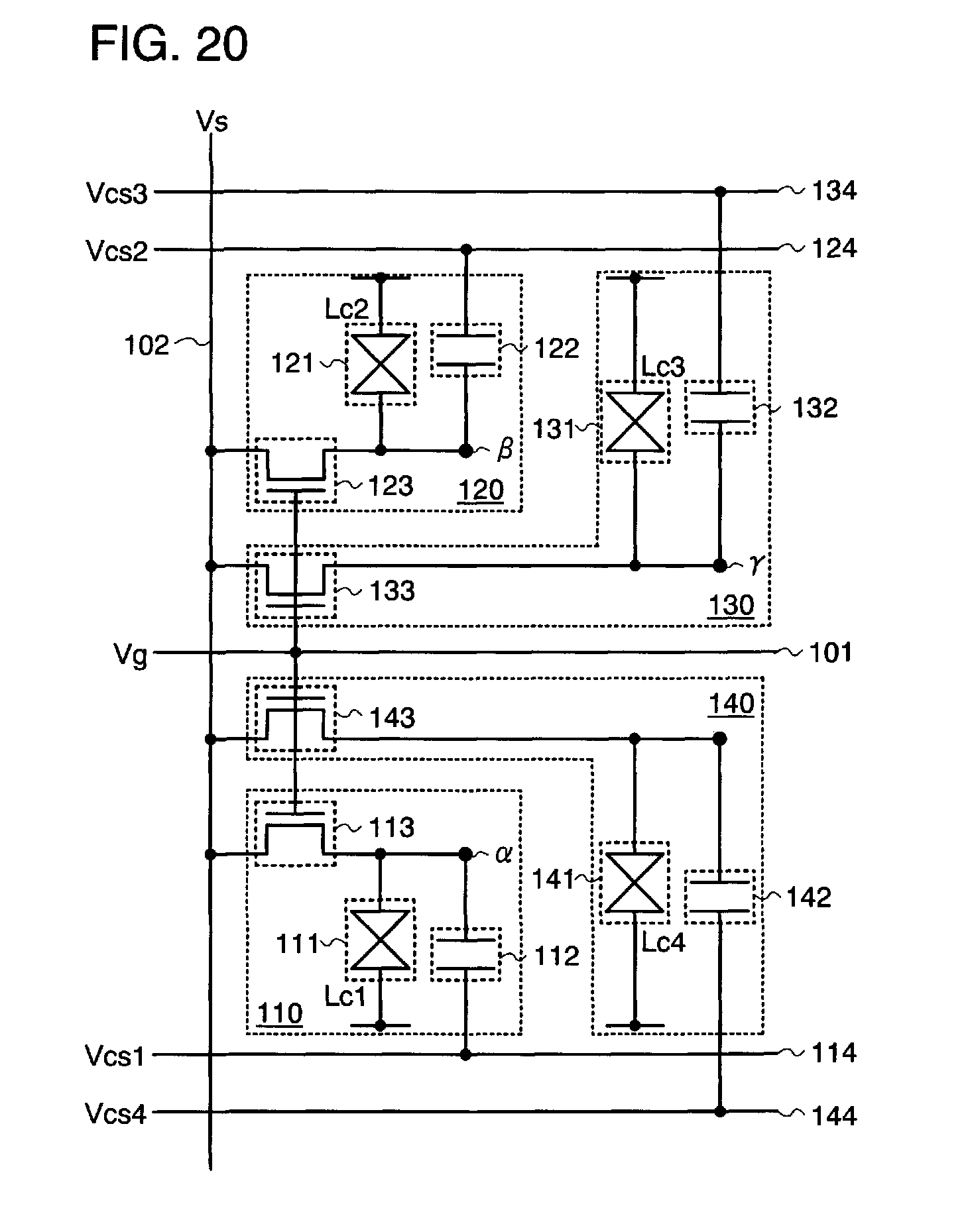
D00021
D00022
D00023
D00024
D00025
D00026
D00027
D00028
D00029
D00030
D00031
D00032
D00033
D00034
D00035

D00036
D00037
D00038

D00039
D00040

D00041
D00042
D00043
D00044
D00045
D00046
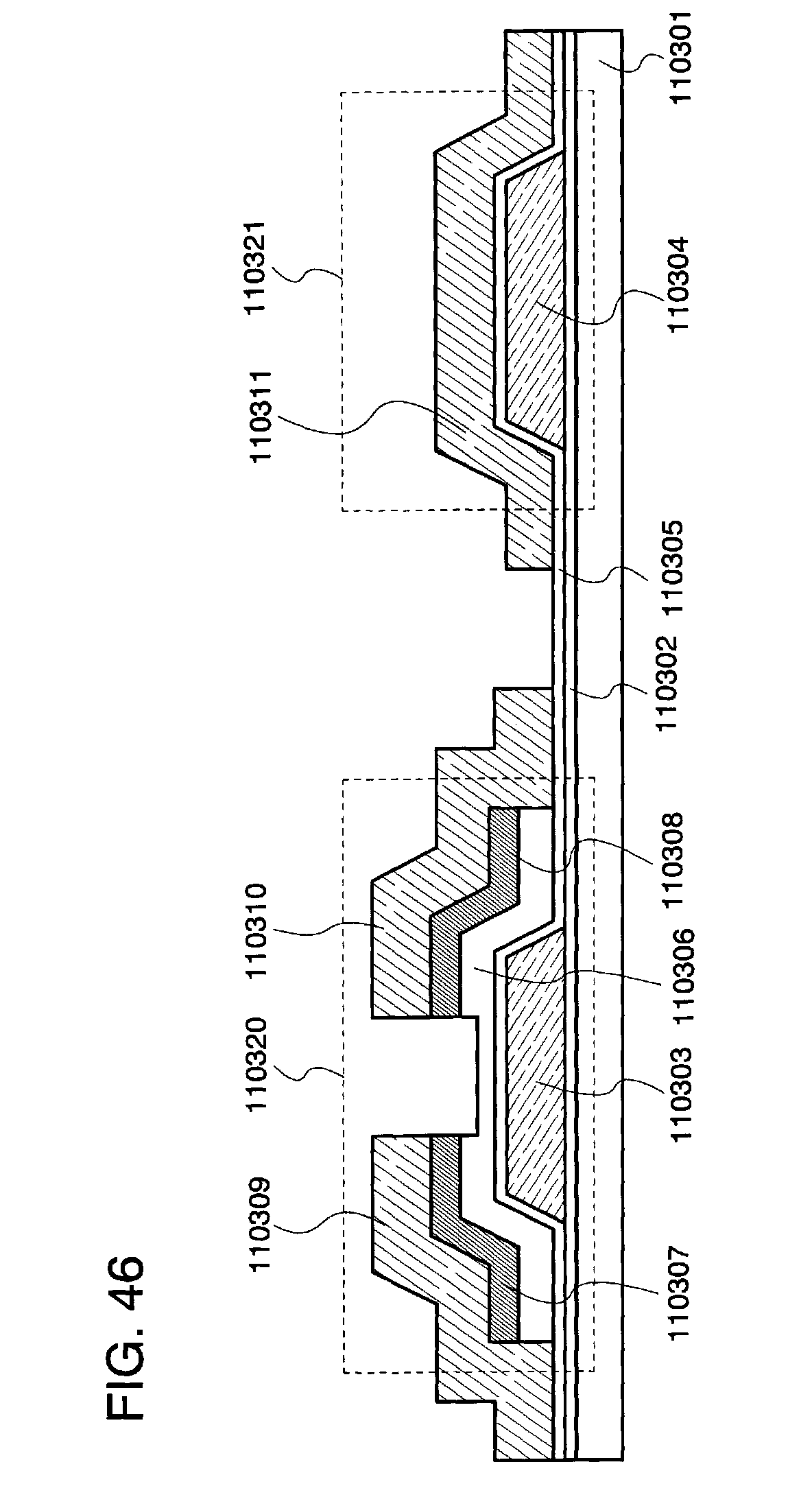
D00047
D00048
D00049
D00050

D00051
D00052
D00053
D00054
D00055
D00056

D00057
D00058

D00059
D00060
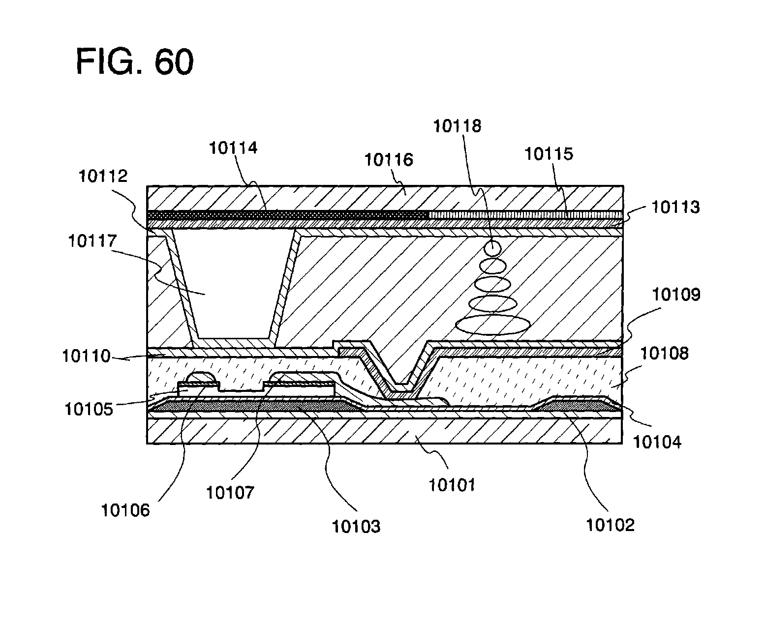
D00061

D00062
D00063
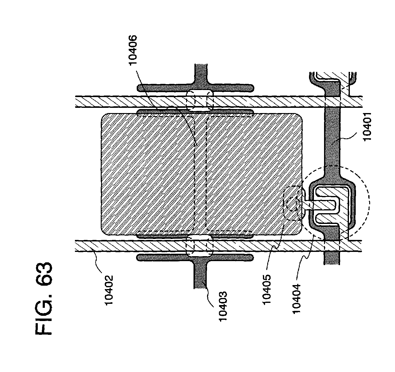
D00064

D00065
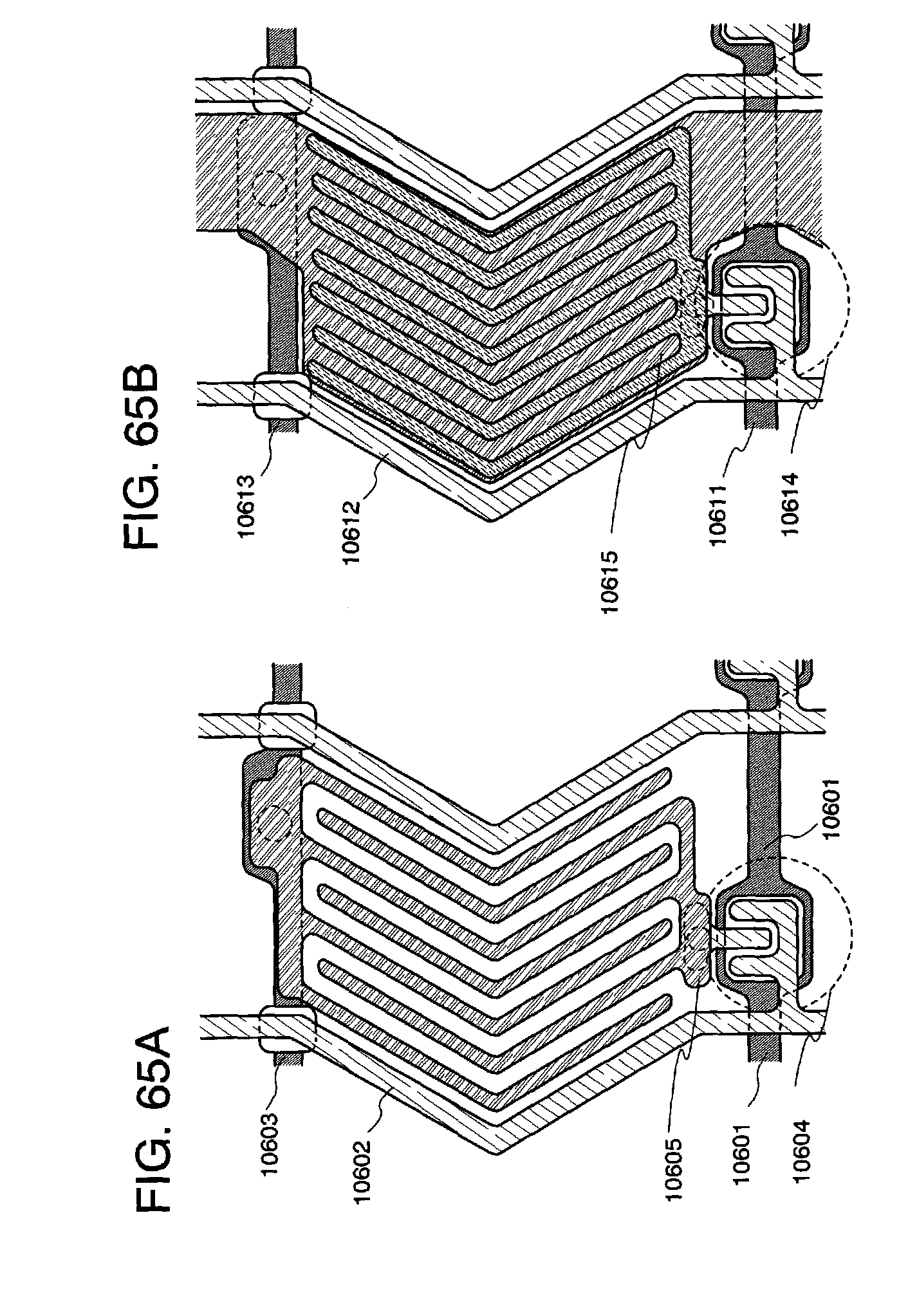
D00066

D00067
D00068
D00069

D00070
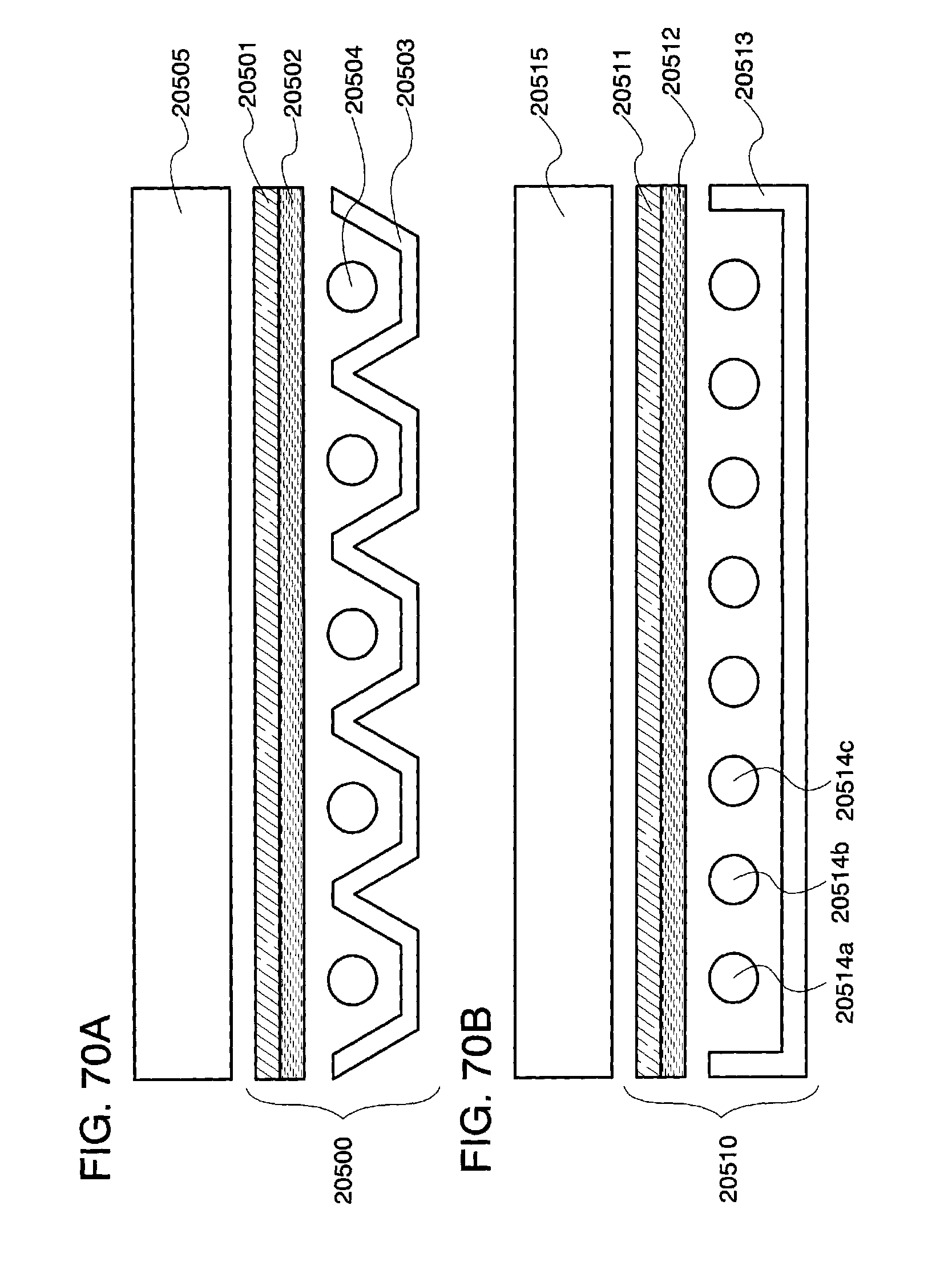
D00071

D00072
D00073

D00074

D00075

D00076

D00077

D00078

D00079

D00080
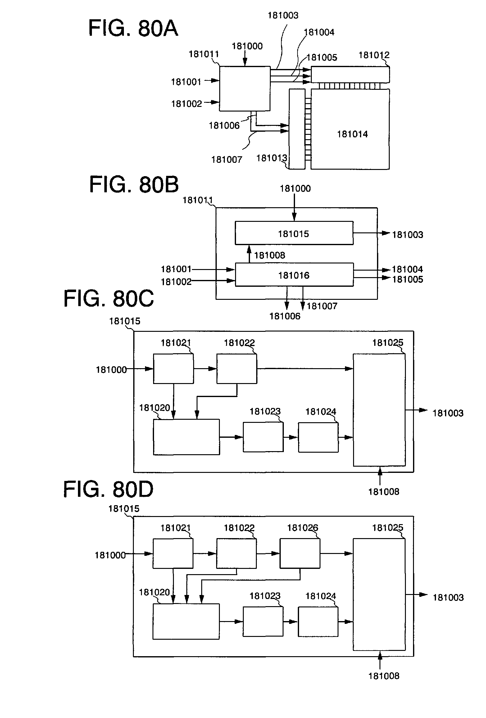
D00081
D00082
D00083

D00084
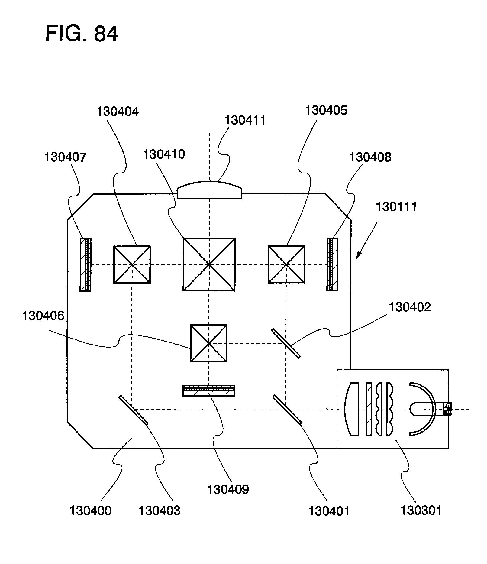
D00085
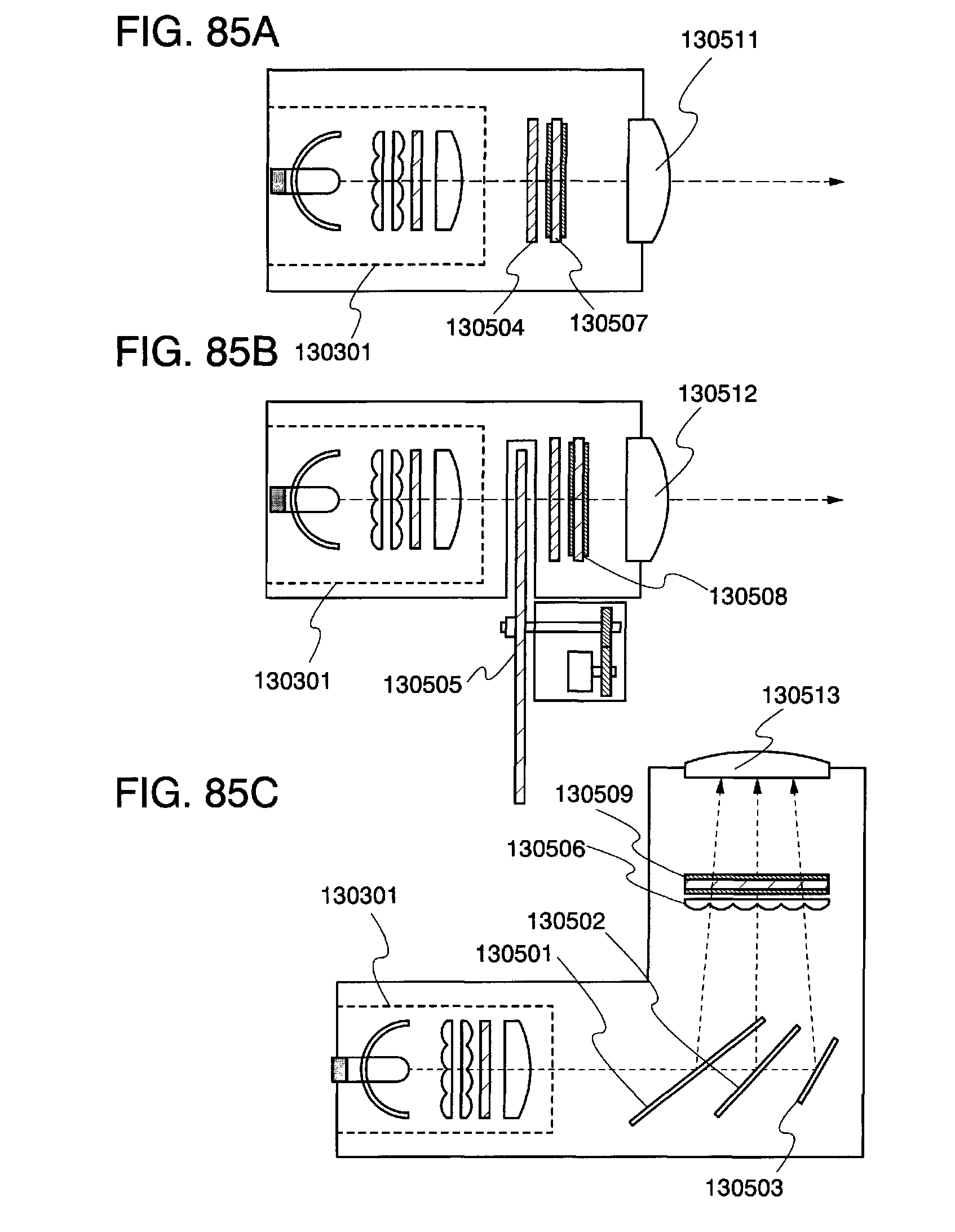
XML
uspto.report is an independent third-party trademark research tool that is not affiliated, endorsed, or sponsored by the United States Patent and Trademark Office (USPTO) or any other governmental organization. The information provided by uspto.report is based on publicly available data at the time of writing and is intended for informational purposes only.
While we strive to provide accurate and up-to-date information, we do not guarantee the accuracy, completeness, reliability, or suitability of the information displayed on this site. The use of this site is at your own risk. Any reliance you place on such information is therefore strictly at your own risk.
All official trademark data, including owner information, should be verified by visiting the official USPTO website at www.uspto.gov. This site is not intended to replace professional legal advice and should not be used as a substitute for consulting with a legal professional who is knowledgeable about trademark law.