Organic light-emitting device
Kim , et al. December 31, 2
U.S. patent number 8,617,721 [Application Number 12/902,315] was granted by the patent office on 2013-12-31 for organic light-emitting device. This patent grant is currently assigned to Samsung Display Co., Ltd.. The grantee listed for this patent is Min-Seung Chun, Dong-Heon Kim, Mi-Kyung Kim, Tae-Shick Kim, Kwan-Hee Lee. Invention is credited to Min-Seung Chun, Dong-Heon Kim, Mi-Kyung Kim, Tae-Shick Kim, Kwan-Hee Lee.


View All Diagrams
| United States Patent | 8,617,721 |
| Kim , et al. | December 31, 2013 |
Organic light-emitting device
Abstract
An organic light-emitting device including a substrate; a first electrode on the substrate; a second electrode; an organic layer between the first electrode and the second electrode, the organic layer including an emission layer; and a first layer including a cyano group-containing compound, the first layer being between the first electrode and the emission layer, wherein the first electrode includes an Al-based reflective layer and a transparent conductive layer sequentially stacked on the substrate, the Al-based reflective layer including a first element and nickel (Ni), and the first element includes at least one of lanthanum (La), cerium (Ce), praseodymium (Pr), promethium (Pm), samarium (Sm), europium (Eu), gadolinium (Gd), terbium (Tb), dysprosium (Dy), holmium (Ho), erbium (Er), thulium (Tm), ytterbium (Yb), and lutetium (Lu).
| Inventors: | Kim; Tae-Shick (Yongin, KR), Kim; Dong-Heon (Yongin, KR), Lee; Kwan-Hee (Yongin, KR), Chun; Min-Seung (Yongin, KR), Kim; Mi-Kyung (Yongin, KR) | ||||||||||
|---|---|---|---|---|---|---|---|---|---|---|---|
| Applicant: |
|
||||||||||
| Assignee: | Samsung Display Co., Ltd.
(Yongin, Gyeonggi-Do, KR) |
||||||||||
| Family ID: | 43417115 | ||||||||||
| Appl. No.: | 12/902,315 | ||||||||||
| Filed: | October 12, 2010 |
Prior Publication Data
| Document Identifier | Publication Date | |
|---|---|---|
| US 20110084258 A1 | Apr 14, 2011 | |
Foreign Application Priority Data
| Oct 12, 2009 [KR] | 10-2009-0096822 | |||
| Current U.S. Class: | 428/690; 428/917; 313/504; 313/506 |
| Current CPC Class: | H01L 51/5271 (20130101); H01L 51/5203 (20130101); H01L 51/5048 (20130101); H01L 51/0059 (20130101); H01L 51/0081 (20130101); H01L 51/0052 (20130101); H01L 51/0079 (20130101); H01L 51/0058 (20130101); H01L 51/0056 (20130101); H01L 51/006 (20130101); H01L 51/0054 (20130101) |
| Current International Class: | H01L 51/50 (20060101) |
References Cited [Referenced By]
U.S. Patent Documents
| 6908783 | June 2005 | Kuehl et al. |
| 7737627 | June 2010 | Hwang et al. |
| 8188315 | May 2012 | Hwang et al. |
| 8339031 | December 2012 | Tchakarov et al. |
| 2002/0117962 | August 2002 | Beierlein et al. |
| 2004/0146744 | July 2004 | Seo et al. |
| 2005/0121667 | June 2005 | Kuehl et al. |
| 2005/0139810 | June 2005 | Kuehl et al. |
| 2005/0173700 | August 2005 | Liao et al. |
| 2005/0221124 | October 2005 | Hwang et al. |
| 2007/0029539 | February 2007 | Yashima et al. |
| 2007/0231503 | October 2007 | Hwang et al. |
| 2007/0264526 | November 2007 | Choi et al. |
| 2008/0012482 | January 2008 | Seo et al. |
| 2008/0014464 | January 2008 | Kawamura et al. |
| 2008/0111484 | May 2008 | Kwon et al. |
| 2008/0121522 | May 2008 | Ehira et al. |
| 2008/0171228 | July 2008 | Chen et al. |
| 2008/0251785 | October 2008 | Noh et al. |
| 2009/0096357 | April 2009 | Lee et al. |
| 2009/0235971 | September 2009 | Pfeiffer et al. |
| 2010/0032186 | February 2010 | Gotou et al. |
| 2010/0072884 | March 2010 | Tchakarov et al. |
| 2011/0084255 | April 2011 | Kim et al. |
| 2011/0084600 | April 2011 | Kim et al. |
| 11-111463 | Apr 1999 | JP | |||
| 2005-167175 | Jun 2005 | JP | |||
| 2005-290000 | Oct 2005 | JP | |||
| 2007-066883 | Mar 2007 | JP | |||
| 2007-201327 | Aug 2007 | JP | |||
| 2008-145647 | Jun 2008 | JP | |||
| 2008-532302 | Aug 2008 | JP | |||
| 2008-216490 | Sep 2008 | JP | |||
| 2009-031752 | Feb 2009 | JP | |||
| 2009-094456 | Apr 2009 | JP | |||
| 2009-175720 | Aug 2009 | JP | |||
| 10-2004-0103672 | Dec 2004 | KR | |||
| 10-2005-0054427 | Jun 2005 | KR | |||
| 10-2005-0097670 | Oct 2005 | KR | |||
| 10-2006-0020156 | Mar 2006 | KR | |||
| 10-2007-0044308 | Apr 2007 | KR | |||
| 10 2007-0109785 | Nov 2007 | KR | |||
| 10-2008-0045629 | May 2008 | KR | |||
| 10-2009-0048241 | May 2009 | KR | |||
| 10-2009-0052351 | May 2009 | KR | |||
| WO 2006/081780 | Aug 2006 | WO | |||
| WO 2008/029060 | Mar 2008 | WO | |||
| WO 2009/081993 | Jul 2009 | WO | |||
Other References
|
European Search Report in EP 10186689.5--1235/2309565, dated Jul. 18, 2012 (Kim, et al.). cited by applicant . Kugimiya, et al.; P-149: Anode electrode of Al-Ni Alloy Film Directly in Contact with ITO for Top-Emitting OLEDs; SID 09 Digest; 2009; pp. 1681-1684; ISSN/009/0966X/09/3903-1681; SID. cited by applicant . European Search Report in EP 10186689.5-1235/2309565, dated Mar. 23, 2012 (Kim et al.). cited by applicant . Japanese Office Action in JP 2010-228945 A, dated Mar. 12, 2013 (Kim, et al.). cited by applicant. |
Primary Examiner: Garrett; Dawn L.
Attorney, Agent or Firm: Lee & Morse, P.C.
Claims
What is claimed is:
1. An organic light-emitting device, comprising: a substrate; a first electrode on the substrate; a second electrode; an organic layer between the first electrode and the second electrode, the organic layer including an emission layer; and a first layer including a cyano group-containing compound and a hole transporting compound, the first layer being between the first electrode and the emission layer and a distance between the first layer and the emission layer being about 50 .ANG. or greater, wherein: the first electrode includes an Al-based reflective layer and a transparent conductive layer sequentially stacked on the substrate, the Al-based reflective layer including a first element and nickel (Ni), the first element includes at least one of lanthanum (La), cerium (Ce), praseodymium (Pr), promethium (Pm), samarium (Sm), europium (Eu), gadolinium (Gd), terbium (Tb), dysprosium (Dy), holmium (Ho), erbium (Er), thulium (Tm), ytterbium (Yb), and lutetium (Lu), and the hole transporting compound includes a compound represented by Formula 41 or 42 below: ##STR00057## wherein R.sub.10 is represented by --(Ar.sub.1).sub.n--Ar.sub.2; R.sub.16 is represented by --(Ar.sub.11).sub.m--Ar.sub.12; Ar.sub.1, Ar.sub.11, L.sub.1, and L.sub.11 are each independently a substituted or unsubstituted C.sub.1-C.sub.30 alkylene group, a substituted or unsubstituted C.sub.2-C.sub.30 alkenylene group, a substituted or unsubstituted C.sub.5-C.sub.30 arylene group, a substituted or unsubstituted C.sub.4-C.sub.30 heteroarylene group, or a group represented by --N(Q.sub.1)-; n, m, a, and b are each independently an integer from 0 to 10; R.sub.1 through R.sub.3, R.sub.11 through R.sub.15, R.sub.17, R.sub.18, R.sub.21 through R.sub.29, Ar.sub.2, Ar.sub.12 and Q.sub.1 are each independently a hydrogen atom, a halogen atom, a hydroxyl group, a cyano group, a substituted or unsubstituted C.sub.1-C.sub.30 alkyl group, a substituted or unsubstituted C.sub.2-C.sub.30 alkenyl group, a substituted or unsubstituted C.sub.2-C.sub.30 alkynyl group, a substituted or unsubstituted C.sub.1-C.sub.30 alkoxy group, a substituted or unsubstituted C.sub.1-C.sub.30 alkylthiol group, a substituted or unsubstituted C.sub.5-C.sub.30 aryl group, a C.sub.4-C.sub.30 heteroaryl group, or a group represented by --N(Q.sub.2)(Q.sub.3); and Q.sub.2 and Q.sub.3 are each independently a hydrogen atom, a halogen atom, a hydroxyl group, a cyano group, a substituted or unsubstituted C.sub.1-C.sub.30 alkyl group, a substituted or unsubstituted C.sub.2-C.sub.30 alkenyl group, a substituted or unsubstituted C.sub.2-C.sub.30 alkynyl group, a substituted or unsubstituted C.sub.1-C.sub.30 alkoxy group, a substituted or unsubstituted C.sub.1-C.sub.30 alkylthiol group, a substituted or unsubstituted C.sub.5-C.sub.30 aryl group, or a substituted or unsubstituted C.sub.4-C.sub.30 heteroaryl group, wherein n groups of Ar.sub.1 in --(Ar.sub.1).sub.n-- are identical to or different from each other, m groups of Ar.sub.11 in --(Ar.sub.11).sub.m-- are identical to or different from each other, a groups of L.sub.1 in -(L.sub.1).sub.a- are identical to or different from each other, and b groups of L.sub.11 in -(L.sub.11).sub.b- are identical to or different from each other.
2. The organic light-emitting device as claimed in claim 1, wherein the first electrode further includes a second element-containing zinc oxide layer, the second element including at least one of aluminum (Al), indium (In), gallium (Ga), germanium (Ge), gadolinium (Gd), zirconium (Zr), molybdenum (Mo), and nickel (Ni).
3. The organic light-emitting device as claimed in claim 2, wherein the Al-based reflective layer, the transparent conductive layer, and the second element-containing zinc oxide layer are sequentially stacked in this order on the substrate.
4. The organic light-emitting device as claimed in claim 2, wherein the second element is included in an amount of about 0.5 to about 10 parts by weight, based on 100 parts by weight of the second element-containing zinc oxide layer.
5. The organic light-emitting device as claimed in claim 2, wherein the Al-based reflective layer includes La, Ni, and Al.
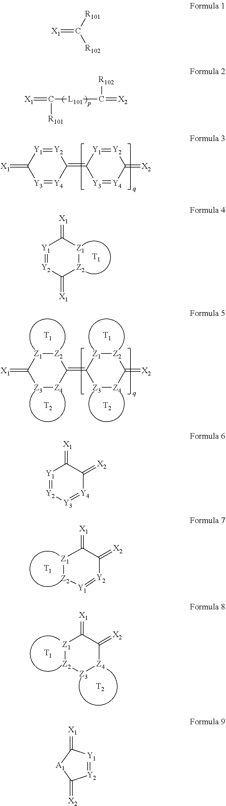
6. The organic light-emitting device as claimed in claim 1, wherein the cyano group-containing compound includes any one of compounds represented by Formulae 1 through 20: ##STR00058## ##STR00059## ##STR00060## in Formulae 1 through 20, X.sub.1 through X.sub.4 are each independently represented by one of Formulae 30A through 30D; Y.sub.1 through Y.sub.8 are each independently N or C(R.sub.103); Z.sub.1 through Z.sub.4 are each independently C or N; A.sub.1 and A.sub.2 are each independently --O--, --S--, --N(R.sub.104), or --C(R.sub.105)(R.sub.106)--; Q.sub.101 and Q.sub.102 are each independently a C.sub.2-C.sub.10 alkylene group, a C.sub.2-C.sub.10 alkenylene group, or a C.sub.2-C.sub.10 alkylene group or C.sub.2-C.sub.10 alkenylene group substituted with at least one of a halogen atom, a cyano group, a hydroxyl group, a C.sub.1-C.sub.10 alkyl group, or a C.sub.1-C.sub.10 alkoxy group; T.sub.1 and T.sub.2 are each independently a C.sub.5-C.sub.30 aromatic ring system, a C.sub.2-C.sub.30 hetero aromatic ring system, or a C.sub.5-C.sub.30 aromatic ring system or C.sub.2-C.sub.30 hetero aromatic ring system substituted with at least one of a halogen atom, a cyano group, a hydroxyl group, a C.sub.1-C.sub.10 alkyl group, and a C.sub.1-C.sub.10 alkoxy group; p is an integer of 1 through 10; q is an integer of 0 through 10; R.sub.101 through R.sub.106 are each independently a hydrogen atom, a halogen atom, a cyano group, a hydroxyl group, a C.sub.1-C.sub.10 alkyl group, a C.sub.1-C.sub.10 alkoxy group, a C.sub.1-C.sub.10 alkyl group substituted with at least one of a halogen atom, a cyano group, a hydroxyl group, a C.sub.5-C.sub.14 aryl group, and a C.sub.2-C.sub.14 hetero aryl group, a C.sub.1-C.sub.10 alkoxy group substituted with at least one of a halogen atom, a cyano group, a hydroxyl group, a C.sub.5-C.sub.14 aryl group, and a C.sub.2-C.sub.14 hetero aryl group, ##STR00061## or --N(R.sub.107)(R.sub.108); R.sub.107 and R.sub.108 are each independently a hydrogen atom, a C.sub.1-C.sub.10 alkyl group, a phenyl group, or a biphenyl group; and L.sub.101 is one of a C.sub.5-C.sub.14 arylene group, a C.sub.5-C.sub.14 hetero arylene group, and a C.sub.5-C.sub.14 arylene group or C.sub.5-C.sub.14 hetero arylene group substituted with at least one of a halogen atom, a cyano group, a hydroxyl group, a C.sub.1-C.sub.10 alkyl group, and a C.sub.1-C.sub.10 alkoxy group: ##STR00062##
7. The organic light-emitting device as claimed in claim 6, wherein X.sub.1 through X.sub.4 are each independently a compound represented by Formula 30A or 30D.
8. The organic light-emitting device as claimed in claim 6, wherein R.sub.103 is one of a hydrogen atom; a halogen atom; a cyano group; a C.sub.1-C.sub.10 alkyl group; a C.sub.1-C.sub.10 alkoxy group; a C.sub.1-C.sub.10 alkyl group or C.sub.1-C.sub.10 alkoxy group substituted with at least one of a halogen atom, a cyano group, a phenyl group, a naphthyl group, an anthryl group, a pyridinyl group, a thiophenyl group, and a benzothiophenyl group; or --N(R.sub.107)(R.sub.108), and wherein R.sub.107 and R.sub.108 are each independently a hydrogen atom, a C.sub.1-C.sub.10 alkyl group, a phenyl group, or a biphenyl group.
9. The organic light-emitting device as claimed in claim 6, wherein R.sub.101 and R.sub.102 are each independently a cyano group, ##STR00063##
10. The organic light-emitting device as claimed in claim 6, wherein each of A.sub.1 and A.sub.2 is --S--.
11. The organic light-emitting device as claimed in claim 6, wherein Q.sub.101 and Q.sub.102 are each independently an ethylene group; a propylene group; an ethenylene group; a prophenylen group; an ethylene group substituted with at least one of a halogen atom, a cyano group, and a hydroxyl group; a propylene group substituted with at least one of a halogen atom, a cyano group, and a hydroxyl group; an ethenylene group substituted with at least one of a halogen atom, a cyano group, and a hydroxyl group; or a prophenylen group substituted with at least one of a halogen atom, a cyano group, and a hydroxyl group.
12. The organic light-emitting device as claimed in claim 6, wherein T.sub.1 and T.sub.2 are each independently benzene; naphthalene; anthracene; thiophene; thiadiazole; oxadiazole; or a benzene, naphthalene, anthracene, thiophene, thiadiazole, or oxadiazole substituted with at least one of a halogen atom, a cyano group, a C.sub.1-C.sub.10 alkyl group, and a C.sub.1-C.sub.10 alkoxy group.
13. The organic light-emitting device as claimed in claim 6, wherein p is 1.
14. The organic light-emitting device as claimed in claim 6, wherein q is 0, 1, or 2.
15. The organic light-emitting device as claimed in claim 6, wherein L.sub.101 is one of a thiophenylene group; a benzothiophenylene group; a thiophenylene group substituted with at least one of a halogen atom, a cyano group, and a C.sub.1-C.sub.10 alkyl group; and a benzothiophenylene group substituted with at least one of a halogen atom, a cyano group, and a C.sub.1-C.sub.10 alkyl group.
16. The organic light-emitting device as claimed in claim 6, wherein the cyano group-containing compound is a compound represented by any one of Formulae 1A through 20B below: ##STR00064## ##STR00065## ##STR00066## ##STR00067## ##STR00068## ##STR00069## ##STR00070## where R.sub.103 and R.sub.109 are each independently a hydrogen atom, --F, a cyano group, a methyl group, an ethyl group, a propyl group, an ethenyl group, a methoxy group, an ethoxy group, or a propoxy group.
17. The organic light-emitting device as claimed in claim 1, wherein Ar.sub.1 and Ar.sub.11 are each independently a C.sub.1-C.sub.10 alkylene group; a phenylene group; a naphthylene group; an anthrylene group; a fluorenylene group; a carbazolylene group; a pyrazolylene group; a pyridinylene group; a triazinylene group; --N(Q.sub.1)-; or a C.sub.1-C.sub.10 alkylene group, phenylene group, naphthylene group, anthrylene group, fluorenylene group, carbazolylene group, pyrazolylene group, pyridinylene group, or triazinylene group substituted with at least one of a halogen atom, a cyano group, a hydroxyl group, a C.sub.1-C.sub.10 alkyl group, a C.sub.1-C.sub.10 alkoxy group, a phenyl group, a naphthyl group, and an anthryl group, wherein Q.sub.1 is one of a hydrogen atom; a C.sub.1-C.sub.10 alkyl group; a C.sub.1-C.sub.10 alkoxy group; a phenyl group; a naphthyl group; a carbazolyl group; a fluorenyl group; a C.sub.1-C.sub.10 alkyl group, C.sub.1-C.sub.10 alkoxy group, phenyl group, naphthyl group, carbazolyl group, or pyrenyl group substituted with at least one substituent selected from the group consisting of a halogen atom, a cyano group, a hydroxyl group, a C.sub.1-C.sub.10 alkyl group, a C.sub.1-C.sub.10 alkoxy group, a phenyl group, a naphthyl group, and an anthryl group; and a fluorenyl group; or --N(Q.sub.2)(Q.sub.3).
18. The organic light-emitting device as claimed in claim 1, wherein Ar.sub.2 and Ar.sub.12 are each independently a hydrogen atom; a C.sub.1-C.sub.10 alkyl group; a phenyl group; a naphthyl group; a carbazolyl group; a fluorenyl group; a pyrenyl group; a C.sub.1-C.sub.10 alkyl group, C.sub.1-C.sub.10 alkoxy group, phenyl group, naphthyl group, carbazolyl group, fluorenyl group, or pyrenyl group substituted with at least one of a halogen atom, a cyano group, a hydroxyl group, a C.sub.1-C.sub.10 alkyl group, a C.sub.1-C.sub.10 alkoxy group, a phenyl group, a naphthyl group, and an anthryl group; or --N(Q.sub.2)(Q.sub.3), and wherein Q.sub.2 and Q.sub.3 are each independently a hydrogen atom, methyl, ethyl, phenyl, methylphenyl, biphenyl, naphthyl, or methylnaphthyl.
19. The organic light-emitting device as claimed in claim 1, wherein n and m are each independently 0, 1, 2, 3, 4, 5, or 6.
20. The organic light-emitting device as claimed in claim 16, wherein the cyano group-containing compound in the first layer is included in an amount of about 0.1 to about 20 parts by weight, based on 100 parts by weight of the first layer.
21. The organic light-emitting device as claimed in claim 1, wherein the first layer has a thickness of about 10 .ANG. to about 2,100 .ANG..
22. The organic light-emitting device as claimed in claim 1, further comprising at least one of a hole injection layer and a hole transport layer between the first layer and the emission layer.
23. The organic light-emitting device as claimed in claim 1, wherein the Al-based reflective layer includes an Al.sub.xNi phase and x is about 2.5 to about 3.5.
24. The organic light-emitting device as claimed in claim 1, wherein the Al.sub.xNi phase, in which x is about 2.5 to about 3.5, contacts the transparent conductive layer.
25. The organic light-emitting device as claimed in claim 24, wherein x is 3.
26. The organic light-emitting device as claimed in claim 1, further comprising a nickel (Ni)-rich oxide layer on a surface of the Al-based reflective layer facing the transparent conductive layer.
27. The organic light-emitting device as claimed in claim 1, wherein the nickel (Ni) in the Al-based reflective layer is included in an amount of about 0.6 wt % to about 5 wt %.
28. The organic light-emitting device as claimed in claim 1, wherein the first element includes lanthanum (La).
29. The organic light-emitting device as claimed in claim 1, wherein the first element in the Al-based reflective layer is included in an amount of about 0.1 wt % to about 3 wt %.
30. The organic light-emitting device as claimed in claim 1, wherein the transparent conductive layer includes indium tin oxide (ITO) or tin oxide (SnO.sub.2).
Description
BACKGROUND
1. Field
Embodiments relate to an organic light-emitting device.
2. Description of the Related Art
Organic light-emitting devices (OLEDs), which are self-emitting devices, have advantages, e.g., a wide viewing angle, excellent contrast, quick response, high brightness, excellent driving voltage characteristics, and can provide multicolored images.
An OLED has a structure including, e.g., a substrate, and an anode, a hole transport layer (HTL), an emission layer (EML), an electron transport layer (ETL), and a cathode, which are sequentially stacked on the substrate. In this regard, the HTL, the EML, and the ETL may be, e.g., organic thin films formed of organic compounds.
An operating principle of an OLED having the above-described structure is as follows.
When a voltage is applied to the anode and the cathode, holes injected from the anode may move to the EML via the HTL; and electrons injected from the cathode may move to the EML via the ETL. The holes and electrons may recombine in the EML to generate excitons. When the excitons drop from an excited state to a ground state, light may be emitted.
SUMMARY
Embodiments are directed to an organic light-emitting device, which substantially overcome one or more of the problems due to the limitations and disadvantages of the related art.
It is a feature of an embodiment to provide an organic light-emitting device having excellent driving voltage characteristics and excellent power efficiency characteristics.
At least one of the above and other features and advantages may be realized by providing an organic light-emitting device including a substrate; a first electrode on the substrate; a second electrode; an organic layer between the first electrode and the second electrode, the organic layer including an emission layer; and a first layer including a cyano group-containing compound, the first layer being between the first electrode and the emission layer, wherein the first electrode includes an Al-based reflective layer and a transparent conductive layer sequentially stacked on the substrate, the Al-based reflective layer including a first element and nickel (Ni), and the first element includes at least one of lanthanum (La), cerium (Ce), praseodymium (Pr), promethium (Pm), samarium (Sm), europium (Eu), gadolinium (Gd), terbium (Tb), dysprosium (Dy), holmium (Ho), erbium (Er), thulium (Tm), ytterbium (Yb), and lutetium (Lu).
The first electrode may further include a second element-containing zinc oxide layer, the second element including at least one of aluminum (Al), indium (In), gallium (Ga), germanium (Ge), gadolinium (Gd), zirconium (Zr), molybdenum (Mo), and nickel (Ni).
The Al-based reflective layer, the transparent conductive layer, and the second element-containing zinc oxide layer may be sequentially stacked in this order on the substrate.
The second element may be included in an amount of about 0.5 to about 10 parts by weight, based on 100 parts by weight of the second element-containing zinc oxide layer.
The Al-based reflective layer may include La, Ni, and Al.
The cyano group-containing compound may include any one of compounds represented by Formulae 1 through 20:
##STR00001## ##STR00002## ##STR00003##
in Formulae 1 through 20,
X.sub.1 through X.sub.4 may each independently be represented by one of Formulae 30A through 30D;
Y.sub.1 through Y.sub.8 may each independently be N or C(R.sub.103);
Z.sub.1 through Z.sub.4 may each independently be C or N;
A.sub.1 and A.sub.2 may each independently be --O--, --S--, --N(R.sub.104), or --C(R.sub.105)(R.sub.106)--;
Q.sub.101 and Q.sub.102 may each independently be a C.sub.2-C.sub.10 alkylene group, a C.sub.2-C.sub.10 alkenylene group, or a C.sub.2-C.sub.10 alkylene group or C.sub.2-C.sub.10 alkenylene group substituted with at least one of a halogen atom, a cyano group, a hydroxyl group, a C.sub.1-C.sub.10 alkyl group, or a C.sub.1-C.sub.10 alkoxy group;
T.sub.1 and T.sub.2 may each independently be a C.sub.5-C.sub.30 aromatic ring system, a C.sub.2-C.sub.30 hetero aromatic ring system, or a C.sub.5-C.sub.30 aromatic ring system or C.sub.2-C.sub.30 hetero aromatic ring system substituted with at least one of a halogen atom, a cyano group, a hydroxyl group, a C.sub.1-C.sub.10 alkyl group, and a C.sub.1-C.sub.10 alkoxy group;
p may be an integer of 1 through 10;
q may be an integer of 0 through 10;
R.sub.101 through R.sub.106 may each independently be a hydrogen atom, a halogen atom, a cyano group, a hydroxyl group, a C.sub.1-C.sub.10 alkyl group, a C.sub.1-C.sub.10 alkoxy group, a C.sub.1-C.sub.10 alkyl group substituted with at least one of a halogen atom, a cyano group, a hydroxyl group, a C.sub.5-C.sub.14 aryl group, and a C.sub.2-C.sub.14 hetero aryl group, a C.sub.1-C.sub.10 alkoxy group substituted with at least one of a halogen atom, a cyano group, a hydroxyl group, a C.sub.5-C.sub.14 aryl group, and a C.sub.2-C.sub.14 hetero aryl group,
##STR00004## or --N(R.sub.107)(R.sub.108); R.sub.107 and R.sub.108 are each independently a hydrogen atom, a C.sub.1-C.sub.10 alkyl group, a phenyl group, or a biphenyl group; and
L.sub.101 may be one of a C.sub.5-C.sub.14 arylene group, a C.sub.5-C.sub.14 hetero arylene group, and a C.sub.5-C.sub.14 arylene group or C.sub.5-C.sub.14 hetero arylene group substituted with at least one of a halogen atom, a cyano group, a hydroxyl group, a C.sub.1-C.sub.10 alkyl group, and a C.sub.1-C.sub.10 alkoxy group:
##STR00005##
X.sub.1 through X.sub.4 may each independently be a compound represented by Formula 30A or 30D.
R.sub.103 may be one of a hydrogen atom; a halogen atom; a cyano group; a C.sub.1-C.sub.10 alkyl group; a C.sub.1-C.sub.10 alkoxy group; a C.sub.1-C.sub.10 alkyl group or C.sub.1-C.sub.10 alkoxy group substituted with at least one of a halogen atom, a cyano group, a phenyl group, a naphthyl group, an anthryl group, a pyridinyl group, a thiophenyl group, and a benzothiophenyl group; or --N(R.sub.107)(R.sub.108), and wherein R.sub.107 and R.sub.108 may each independently be a hydrogen atom, a C.sub.1-C.sub.10 alkyl group, a phenyl group, or a biphenyl group.
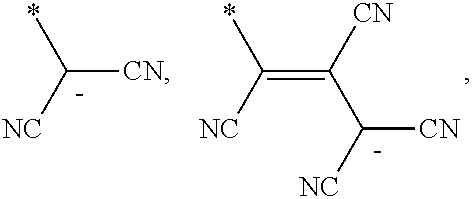
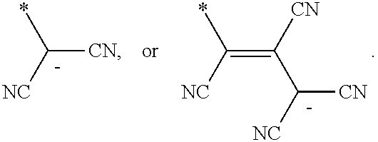
R.sub.101 and R.sub.102 may each independently be a cyano group,
##STR00006##
Each of A.sub.1 and A.sub.2 may be --S--.
Q.sub.101 and Q.sub.102 may each independently be an ethylene group; a propylene group; an ethenylene group; a prophenylen group; an ethylene group substituted with at least one of a halogen atom, a cyano group, and a hydroxyl group; a propylene group substituted with at least one of a halogen atom, a cyano group, and a hydroxyl group; an ethenylene group substituted with at least one of a halogen atom, a cyano group, and a hydroxyl group; or a prophenylen group substituted with at least one of a halogen atom, a cyano group, and a hydroxyl group.
T.sub.1 and T.sub.2 may each independently be benzene; naphthalene; anthracene;
thiophene; thiadiazole; oxadiazole; or a benzene, naphthalene, anthracene, thiophene, thiadiazole, or oxadiazole substituted with at least one of a halogen atom, a cyano group, a C.sub.1-C.sub.10 alkyl group, and a C.sub.1-C.sub.10 alkoxy group.
p may be 1.
q may be 0, 1, or 2.
L.sub.101 may be one of a thiophenylene group; a benzothiophenylene group; a thiophenylene group substituted with at least one of a halogen atom, a cyano group, and a C.sub.1-C.sub.10 alkyl group; and a benzothiophenylene group substituted with at least one of a halogen atom, a cyano group, and a C.sub.1-C.sub.10 alkyl group.
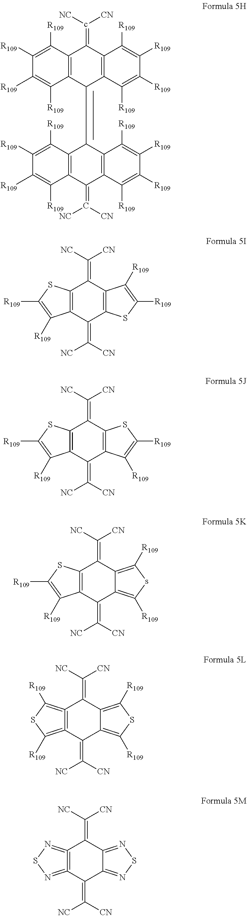
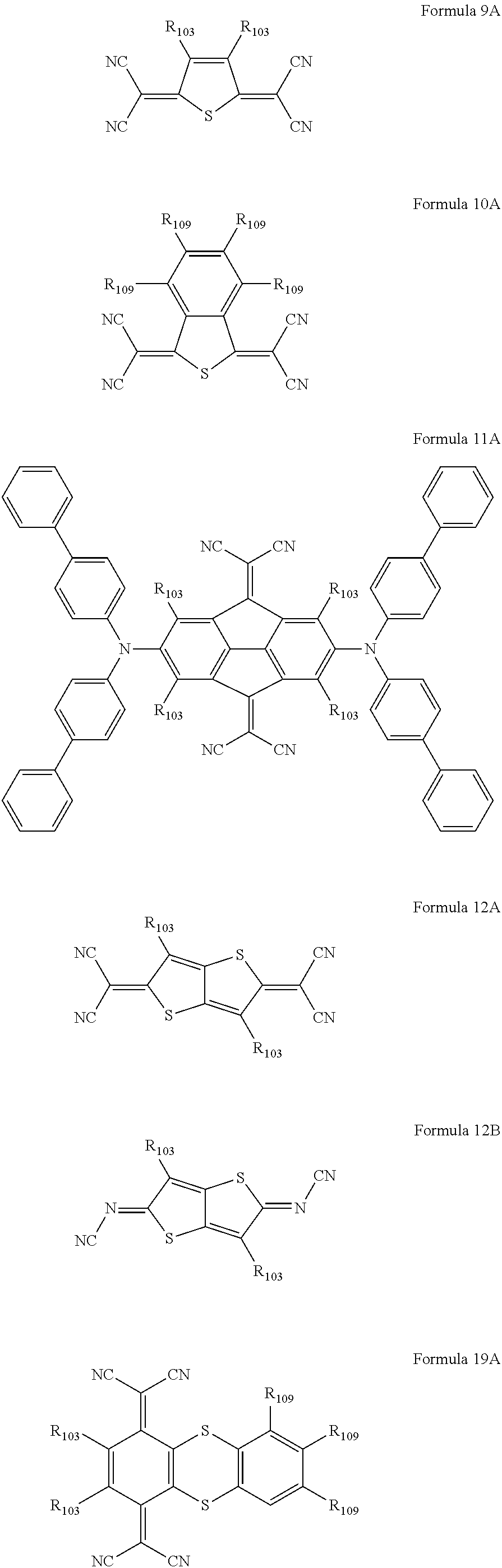
The cyano group-containing compound may be a compound represented by any one of Formulae 1A through 20B below:
##STR00007## ##STR00008## ##STR00009## ##STR00010## ##STR00011## ##STR00012##
where R.sub.103 and R.sub.109 may each independently be a hydrogen atom, --F, a cyano group, a methyl group, an ethyl group, a propyl group, an ethenyl group, a methoxy group, an ethoxy group, or a propoxy group.
The first layer may further include a hole transporting compound.
The hole transporting compound may include a compound represented by Formula 41 or 42 below:
##STR00013##
wherein R.sub.10 may be represented by --(Ar.sub.1).sub.n--Ar.sub.2;
R.sub.16 may be represented by --(Ar.sub.11).sub.m--Ar.sub.12;
Ar.sub.1, Ar.sub.11, L.sub.1, and L.sub.11 may each independently be a substituted or unsubstituted C.sub.1-C.sub.30 alkylene group, a substituted or unsubstituted C.sub.2-C.sub.30 alkenylene group, a substituted or unsubstituted C.sub.5-C.sub.30 arylene group, a substituted or unsubstituted C.sub.4-C.sub.30 heteroarylene group, or a group represented by --N(Q.sub.1)-;
n, m, a, and b may each independently be an integer from 0 to 10;
R.sub.1 through R.sub.3, R.sub.11 through R.sub.15, R.sub.17, R.sub.18, R.sub.21 through R.sub.29, Ar.sub.2, Ar.sub.12 and Q.sub.1 may each independently be a hydrogen atom, a halogen atom, a hydroxyl group, a cyano group, a substituted or unsubstituted C.sub.1-C.sub.30 alkyl group, a substituted or unsubstituted C.sub.2-C.sub.30 alkenyl group, a substituted or unsubstituted C.sub.2-C.sub.30 alkynyl group, a substituted or unsubstituted C.sub.1-C.sub.30 alkoxy group, a substituted or unsubstituted C.sub.1-C.sub.30 alkylthiol group, a substituted or unsubstituted C.sub.5-C.sub.30 aryl group, a C.sub.4-C.sub.30 heteroaryl group, or a group represented by --N(Q.sub.2)(Q.sub.3); and
Q.sub.2 and Q.sub.3 may each independently be a hydrogen atom, a halogen atom, a hydroxyl group, a cyano group, a substituted or unsubstituted C.sub.1-C.sub.30 alkyl group, a substituted or unsubstituted C.sub.2-C.sub.30 alkenyl group, a substituted or unsubstituted C.sub.2-C.sub.30 alkynyl group, a substituted or unsubstituted C.sub.1-C.sub.30 alkoxy group, a substituted or unsubstituted C.sub.1-C.sub.30 alkylthiol group, a substituted or unsubstituted C.sub.5-C.sub.30 aryl group, or a substituted or unsubstituted C.sub.4-C.sub.30heteroaryl group,
wherein n groups of Ar.sub.1 in --(Ar.sub.1).sub.n-- may be identical to or different from each other, m groups of Ar.sub.11 in --(Ar.sub.11).sub.m-- may be identical to or different from each other, a groups of L.sub.1 in -(L.sub.1).sub.a--may be identical to or different from each other, and b groups of L.sub.11 in -(L.sub.11).sub.b- may be identical to or different from each other.
Ar.sub.1 and Ar.sub.11 may each independently be a C.sub.1-C.sub.10 alkylene group; a phenylene group; a naphthylene group; an anthrylene group; a fluorenylene group; a carbazolylene group; a pyrazolylene group; a pyridinylene group; a triazinylene group; --N(Q.sub.1)-; or a C.sub.1-C.sub.10 alkylene group, phenylene group, naphthylene group, anthrylene group, fluorenylene group, carbazolylene group, pyrazolylene group, pyridinylene group, or triazinylene group substituted with at least one of a halogen atom, a cyano group, a hydroxyl group, a C.sub.1-C.sub.10 alkyl group, a C.sub.1-C.sub.10 alkoxy group, a phenyl group, a naphthyl group, and an anthryl group, and wherein Q.sub.1 may be one of a hydrogen atom; a C.sub.1-C.sub.10 alkyl group; a C.sub.1-C.sub.10 alkoxy group; a phenyl group; a naphthyl group; a carbazolyl group; a fluorenyl group; a C.sub.1-C.sub.10 alkyl group, C.sub.1-C.sub.10 alkoxy group, phenyl group, naphthyl group, carbazolyl group, or pyrenyl group substituted with at least one substituent selected from the group consisting of a halogen atom, a cyano group, a hydroxyl group, a C.sub.1-C.sub.10 alkyl group, a C.sub.1-C.sub.10 alkoxy group, a phenyl group, a naphthyl group, and an anthryl group; and a fluorenyl group; or --N(Q.sub.2)(Q.sub.3).
Ar.sub.2 and Ar.sub.12 may each independently be a hydrogen atom; a C.sub.1-C.sub.10 alkyl group; a phenyl group; a naphthyl group; a carbazolyl group; a fluorenyl group; a pyrenyl group; a C.sub.1-C.sub.10 alkyl group, C.sub.1-C.sub.10 alkoxy group, phenyl group, naphthyl group, carbazolyl group, fluorenyl group, or pyrenyl group substituted with at least one of a halogen atom, a cyano group, a hydroxyl group, a C.sub.1-C.sub.10 alkyl group, a C.sub.1-C.sub.10 alkoxy group, a phenyl group, a naphthyl group, and an anthryl group; or --N(Q.sub.2)(Q.sub.3), and wherein Q.sub.2 and Q.sub.3 may each independently be a hydrogen atom, methyl, ethyl, phenyl, methylphenyl, biphenyl, naphthyl, or methylnaphthyl.
n and m may each independently be 0, 1, 2, 3, 4, 5, or 6.
The cyano group-containing compound in the first layer may be included in an amount of about 0.1 to about 20 parts by weight, based on 100 parts by weight of the first layer.
The first layer may have a thickness of about 10 .ANG. to about 2,100 .ANG..
A distance between the first layer and the emission layer may be about 50 .ANG. or greater.
The organic light-emitting device may further include at least one of a hole injection layer and a hole transport layer between the first layer and the emission layer.
The Al-based reflective layer may include an Al.sub.xNi phase and x may be about 2.5 to about 3.5.
The Al.sub.xNi phase, in which x is about 2.5 to about 3.5, may contact the transparent conductive layer.
x may be 3.
The organic light-emitting device may further include a nickel (Ni)-rich oxide layer on a surface of the Al-based reflective layer facing the transparent conductive layer.
The nickel (Ni) in the Al-based reflective layer may be included in an amount of about 0.6 wt % to about 5 wt %.
The first element may include lanthanum (La).
The first element in the Al-based reflective layer may be included in an amount of about 0.1 wt % to about 3 wt %.
The transparent conductive layer may include indium tin oxide (ITO) or tin oxide (SnO.sub.2).
BRIEF DESCRIPTION OF THE DRAWINGS
The above and other features and advantages will become more apparent to those of ordinary skill in the art by describing in detail exemplary embodiments with reference to the attached drawings, in which:
FIG. 1 illustrates a cross-sectional view of a structure of an organic light-emitting device (OLED) according to an embodiment;
FIG. 2A illustrates a transmission electron microscopic (TEM) image of a cross-section of an aluminum (Al)-based reflective layer according to an embodiment;
FIG. 2B illustrates a scanning transmission electrode microscope
(STEM)-high angle annular dark-field image of the aluminum (Al)-based reflective film shown in FIG. 2A;
FIG. 2C illustrates a result of energy dispersive X-ray spectroscopy on abnormally grown crystals in FIG. 2A;
FIG. 3 illustrates a TEM image of a cross-section of a first electrode according to another embodiment; and
FIG. 4 illustrates is a cross-sectional view of a structure of an OLED according to another embodiment.
DETAILED DESCRIPTION
Korean Patent Application No. 10-2009-0096822, filed on Oct. 12, 2009, in the Korean Intellectual Property Office, and entitled: "Organic Light-Emitting Device," is incorporated by reference herein in its entirety.
Example embodiments will now be described more fully hereinafter with reference to the accompanying drawings; however, they may be embodied in different forms and should not be construed as limited to the embodiments set forth herein. Rather, these embodiments are provided so that this disclosure will be thorough and complete, and will fully convey the scope of the invention to those skilled in the art.
In the drawing figures, the dimensions of layers and regions may be exaggerated for clarity of illustration. It will also be understood that when a layer or element is referred to as being "on" another layer or substrate, it can be directly on the other layer or substrate, or intervening layers may also be present. In addition, it will also be understood that when a layer is referred to as being "between" two layers, it can be the only layer between the two layers, or one or more intervening layers may also be present. Like reference numerals refer to like elements throughout.
FIG. 1 illustrates a schematic sectional view of an organic light-emitting device (OLED) 10 according to an embodiment. Referring to FIG. 1, the OLED 10 according to the present embodiment may include a substrate 1, a first electrode 5, a first layer 6 containing a cyano-group containing compound, an organic layer 7, and a second electrode 9, which may be sequentially stacked in this order. The first electrode 5 may include an aluminum (Al)-based reflective layer 5a and a transparent conductive layer 5b sequentially stacked on the substrate. The Al-based reflective layer 5a may include, e.g., a first element and nickel (Ni).
The substrate 1, which may be any suitable substrate that is used for organic light emitting devices, may be, e.g., a glass substrate or a transparent plastic substrate with excellent mechanical strength, thermal stability, transparency, surface smoothness, ease of handling, and water-repellent properties.
The first element in the Al-based reflective layer 5a may include at least one of, e.g., lanthanum (La), cerium (Ce), praseodymium (Pr), promethium (Pm), samarium (Sm), europium (Eu), gadolinium (Gd), terbium (Tb), dysprosium (Dy), holmium (Ho), erbium (Er), thulium (Tm), ytterbium (Yb), and lutetium (Lu).
The Al-based reflective layer 5a may have a high reflectance, and thus may improve luminescent efficiency of the OLED. In addition, the Al-based reflective layer 5a may have high thermal stability due to properties of Al. Thus, the Al-based reflective layer 5a may have excellent durability even when exposed to a high-temperature manufacturing process. In addition, the Al-based reflective layer 5a may have excellent adhesive characteristics with respect to an organic layer or an inorganic layer adjacent thereto.
Therefore, the Al-based reflective layer and the transparent ITO conductive layer may be substantially not separated in a cathode junction region.
The Al-based reflective layer 5a and the transparent conductive layer 5b may contact each other. However, undesirable galvanic corrosion caused due to a potential difference between the Al-based reflective layer 5a and the transparent conductive layer 5b may substantially not occur.
Galvanic corrosion may occur due to a potential difference between two different metals adjacent to each other, thereby causing current to flow and electricity to be generated. One of such two different metals electrically in contact with each other having a relatively greater activity (lower potential) due to their different work functions at an interface thereof may function as a cathode; and the other one having a relatively lower activity (greater potential) may function as an anode. When the two metals are exposed to a corrosive solution, both the metals may be corroded due to the potential difference thereof. This is referred to as galvanic corrosion. The cathode having a greater activity may be corroded faster than when exclusively used; and the anode having a lower activity may be corroded slower than when exclusively used. As such galvanic corrosion spreads along the interface of the two electrode layers formed of different metals, contact resistance between the two electrodes may be abruptly increased. Thus, the contact resistance may be very unstably distributed. Accordingly, when an OLED including two such electrode layers is operated, pixels of the OLED may display colors with inconsistent luminance. Due to this non-uniform luminance, image quality may be significantly lowered. As such, galvanic corrosion may be a quality deterioration factor in OLEDs.
However, since the Al-based reflective layer 5a includes the first element, which will be described below in detail, such galvanic corrosion may substantially not occur between the Al-based reflective layer 5a and the transparent conductive layer 5b. Thus, the OLED according to the present embodiment may be of excellent quality.
The Al-based reflective layer 5a may include, e.g., nickel (Ni). Thus, the Al-based reflective layer 5a may include an Al.sub.xNi phase wherein x is about 2.5 to about 3.5.
FIG. 2A illustrates a transmission electron microscopic (TEM) image of a cross-section of an Al-based reflective layer (layer A) formed on a titanium (Ti) layer (layer B), wherein the Al-based reflective layer includes 2 wt % of nickel (Ni) and 0.35 wt % of lanthanum (La). FIG. 2B illustrates a scanning transmission electrode microscope (STEM)-high angle annular dark-field image of the aluminum (Al)-based reflective film shown in FIG. 2A. FIG. 2C illustrates a result of semi-quantitative energy dispersive X-ray spectroscopy (EDS) on abnormally grown crystals (at first and second measurement sites) appearing in gray in FIG. 2A. As illustrated in FIG. 2C, the abnormally grown crystals in FIG. 2A includes Al and Ni in a ratio of Al(K):Ni(K)=73:27 (in atom %). Thus, the Al-based reflective layer presumably includes an Al.sub.xNi phase wherein x is about 3.
The Al.sub.xNi phase, wherein x is about 2.5 to about 3.5, may contact the transparent conductive layer 5b.
In addition, a Ni-rich oxide layer may be further disposed on a surface of the Al-based reflective layer 5a facing the transparent conductive layer 5b.
FIG. 3 illustrates a TEM image of a cross-section of a structure including an Al-based reflective layer (region C) and a transparent ITO conductive layer (region D) sequentially formed on a TFT substrate, wherein the Al-based reflective layer includes 2 wt % of nickel (Ni) and 0.35 wt % of lanthanum (La). In FIG. 3, a linear region, denoted by "E`, between the Al-based reflective layer and the transparent ITO conductive layer, corresponds to a Ni-rich oxide layer having a thickness of about 7 nm to about 8 nm.
Due to the Al.sub.xNi phase, wherein x is about 2.5 to about 3.5 and/or the Ni-rich oxide layer described above, ohmic contact may be realized between the Al-based reflective layer 5a and the transparent conductive layer 5b.
The Ni may be included in the Al-based reflective layer 5a in an amount of about 0.6 wt % to about 5 wt %, e.g., about 1 wt % to about 4 wt %. Maintaining the amount of Ni in the Al-based reflective layer 5a at about 0.6 wt % to about 5 wt % may help ensure that the contact resistance between the Al-based reflective layer 5a and the transparent conductive layer 5b is stabilized and reflectivity and durability to chemicals of the Al-based reflective layer 5a is substantially not reduced. In an implementation, the amount of Ni in the Al-based reflective layer 5a may be about 2 wt %. However, the amount of Ni in the Al-based reflective layer 5a is not limited to these amounts.
The Al-based reflective layer 5a may include the first element, in addition to Ni having such a function as described above. The first element may include at least one of, e.g., lanthanum (La), cerium (Ce), praseodymium (Pr), promethium (Pm), samarium (Sm), europium (Eu), gadolinium (Gd), terbium (Tb), dysprosium (Dy), holmium (Ho), erbium (Er), thulium (Tm), ytterbium (Yb), and lutetium (Lu).
Since the Al-based reflective layer 5a may include such a first element as listed above, the Al-based reflective layer 5a may have excellent thermal stability and galvanic corrosion may be suppressed. For example, the first element may include lanthanum (La), but is not limited thereto.
The first element may be included in an amount of about 0.1 wt % to about 3 wt %, e.g., about 0.1 wt % to about 1 wt %. Maintaining the amount of the first element at about 0.1 wt % to about 3 wt % may help ensure that neither thermal stability of Al in the Al-based reflective layer 5a nor reflectivity of the Al-based reflective layer 5 are substantially reduced. The amount of the first element is not limited to the above range. For example, the first element may be included in an amount of about 0.3 wt % to about 0.35 wt %, but is not limited thereto.
The Al-based reflective layer 5a may have a thickness of about 50 nm or greater, e.g., about 100 nm to about 500 nm. Maintaining the thickness of the Al-based reflective layer 5a at about 50 nm or greater may help ensure that a decrease in luminescent efficiency caused by passage of light generated in the organic layer 7 through the Al-based reflective layer 5a is substantially prevented.
The transparent conductive layer 5b may be formed of, e.g., a transparent conductive metal oxide. Examples of transparent conductive metal oxides include ITO and tin oxide (SnO.sub.2), but are not limited thereto. In an implementation, the transparent conductive layer 5b may be formed of ITO.
The transparent conductive layer 5b may have a thickness of about 5 nm to about 100 nm, e.g., about 7 nm to about 80 nm. Maintaining the thickness of the transparent conductive layer 5b at about 5 nm to about 100 nm may help ensure that a reduction in the reflectivity of the Al-based reflective layer 5a is minimized and that the OLED has excellent efficiency.
The first layer 6 containing a cyano-group containing compound may be formed on the transparent conductive layer 5b. Since the cyano group-containing compound contained in the first layer 6 has two types of one electron reduction state, the cyano group-containing compound may have an extended .pi.-electronic system capable of forming a stable radical (identifiable by, e.g., cyclic voltammetry). Thus, the first layer 6 may lower a hole injection barrier from the first electrode 5 to the organic layer 7. Thus, holes may be easily injected from the first electrode 5 to the organic layer 7. Accordingly, an OLED including the first layer 6 containing a cyano-group containing compound may have excellent driving voltage characteristics and excellent power efficiency characteristics.
The cyano group-containing compound contained in the first layer 6 may include one of the compounds represented by Formulae 1 through 20 below.
##STR00014## ##STR00015## ##STR00016##
In Formulae 1 through 20, X.sub.1 through X.sub.4 may each independently be represented by one of Formulae 30A through 30D; Y.sub.1 through Y.sub.8 may each independently be N or C(R.sub.103); Z.sub.1 through Z.sub.4 may each independently be C or N; A.sub.1 and A.sub.2 may each independently be --O--, --S--, --N(R.sub.104), or --C(R.sub.105)(R.sub.106)--; Q.sub.101 and Q.sub.102 may each independently be a C.sub.2-C.sub.10 alkylene group, a C.sub.2-C.sub.10 alkenylene group, or a C.sub.2-C.sub.10 alkylene group or C.sub.2-C.sub.10 alkenylene group substituted with at least one of a halogen atom, a cyano group, a hydroxyl group, a C.sub.1-C.sub.10 alkyl group, and a C.sub.1-C.sub.10 alkoxy group; T.sub.1 and T.sub.2 may each independently be a C.sub.5-C.sub.30 aromatic ring system, a C.sub.2-C.sub.30 hetero aromatic ring system, or a C.sub.5-C.sub.30 aromatic ring system or C.sub.2-C.sub.30 hetero aromatic ring system substituted with at least one of a halogen atom, a cyano group, a hydroxyl group, a C.sub.1-C.sub.10 alkyl group, and a C.sub.1-C.sub.10 alkoxy group; p may be an integer of 1 through 10; q may be an integer of 0 through 10; R.sub.101 through R.sub.106 may each independently be a hydrogen atom, a halogen atom, a cyano group, a hydroxyl group, a C.sub.1-C.sub.10 alkyl group, a C.sub.1-C.sub.10 alkoxy group, a C.sub.1-C.sub.10 alkyl group substituted with at least one of a halogen atom, a cyano group, a hydroxyl group, a C.sub.5-C.sub.14 aryl group, and a C.sub.2-C.sub.14 hetero aryl group, a C.sub.1-C.sub.10 alkoxy group substituted with at least one of a halogen atom, a cyano group, a hydroxyl group, a C.sub.5-C.sub.14 aryl group, and a C.sub.2-C.sub.14 hetero aryl group,
##STR00017## or --N(R.sub.107)(R.sub.108); R.sub.107 and R.sub.108 may each independently be a hydrogen atom, a C.sub.1-C.sub.10 alkyl group, a phenyl group, or a biphenyl group; and L.sub.101 may be a C.sub.5-C.sub.14 arylene group, a C.sub.5-C.sub.14 hetero arylene group, and a C.sub.2-C.sub.10 alkenylene group, C.sub.5-C.sub.14 arylene group, or C.sub.5-C.sub.14 hetero arylene group substituted with at least one a halogen atom, a cyano group, a hydroxyl group, a C.sub.1-C.sub.10 alkyl group, or a C.sub.1-C.sub.10 alkoxy group:
##STR00018##
For example, in Formulae 1 through 20, X.sub.1 through X.sub.4 may be represented by Formula 30A or 30D.
For example, in Formulae 1 through 20, R.sub.103 may be a hydrogen atom; a halogen atom; a cyano group; a C.sub.1-C.sub.10 alkyl group; a C.sub.1-C.sub.10 alkoxy group; a C.sub.1-C.sub.10 alkyl group or C.sub.1-C.sub.10 alkoxy group substituted with at least one of a halogen atom, a cyano group, a phenyl group, a naphthyl group, an anthryl group, a pyridinyl group, and a thiophenyl group, and a benzothiophenyl group; or --N(R.sub.107)(R.sub.108) where R.sub.107 and R.sub.108 are each independently a hydrogen atom, a C.sub.1-C.sub.10 alkyl group, a phenyl group, or a biphenyl group.
For example, R.sub.103 may be a hydrogen atom, --F, a cyano group, a methyl group, an ethyl group, a propyl group, an ethenyl group, a methoxy group, an ethoxy group, a propoxy group, a methyl group substituted with phenyl, a propyl group substituted with phenyl, or a --N(biphenyl group)(biphenyl group), but is not limited thereto.
In Formulae 1 and 2, R.sub.101 and R.sub.102 may each independently be a cyano group,
##STR00019## but is not limited thereto.
The compound of Formula 1 may be Compound 20 below, but is not limited thereto:
In Formulae 1 through 20, A.sub.1 and A.sub.2 may be --S--, but is not limited thereto.
In Formula 20, Q.sub.101 and Q.sub.102 may each independently be an ethylene group; a propylene group; an ethenylene group; a prophenylen group; an ethylene group substituted with at least one of a halogen atom, a cyano group, and a hydroxyl group; a propylene group substituted with at least one of a halogen atom, a cyano group, and a hydroxyl group; an ethenylene group substituted with at least one of a halogen atom, a cyano group, and a hydroxyl group; or a prophenylene group substituted with at least one of a halogen atom, a cyano group, and a hydroxyl group. For example, Q.sub.101 and Q.sub.102 may each independently be an ethylene group; an ethenylene group; an ethylene group substituted with at least one of --F and a cyano group; and an ethenylene group substituted with at least one of --F and a cyano group, but is not limited thereto.
In Formulae 1 through 20, each of T.sub.1 and T.sub.2 may be a C.sub.5-C.sub.30 aromatic ring system; a C.sub.2-C.sub.30 hetero aromatic ring system; or a C.sub.5-C.sub.30 aromatic ring system or C.sub.5-C.sub.30 hetero aromatic ring system substituted with at least one of a halogen atom, a cyano group, a hydroxyl group, a C.sub.1-C.sub.10 alkyl group, or a C.sub.1-C .sub.10 alkoxy group, wherein each of these systems includes Z.sub.1 and Z.sub.2 or Z.sub.3 and Z.sub.4 as constituent elements. As illustrated in Formulae 1 through 20, each of T.sub.1 and T.sub.2 may be fused at one or more sites of a backbone of the compounds represented by Formulae 1 through 20.
The C.sub.5-C.sub.30 aromatic ring system refers to a carbocyclic aromatic system that contains at least one aromatic ring and 5 through 30 carbon atoms. In this regard, the term "system" is adopted to represent that C.sub.5-C.sub.30 aromatic ring system also includes a multi-ring structure. When the aromatic ring system includes 2 or more rings, the 2 or more rings may be fused together or connected to each other through a single bond. In an implementation, the aromatic ring system may be a C.sub.6-C.sub.30 aromatic ring system. The C.sub.2-C.sub.30 hetero aromatic ring system refers to a heterocyclic aromatic system that contains at least one aromatic ring and 2 through 30 carbon atoms. For example, the C.sub.2-C.sub.30 hetero aromatic ring system may include at least one hetero atom selected from the group consisting of nitrogen (N), oxygen (O), phosphorous (P), and sulfur (S), and the other ring atoms are carbons (C). If the C.sub.2-C.sub.30 hetero aromatic ring system further includes, in addition to a hetero aromatic ring, at least one of an aromatic ring and a hetero aromatic ring, these rings may be fused to each other.Examples of the C.sub.5-C.sub.30 aromatic ring system include benzene, pentalene, indene, naphthalene, azulene, heptalene, indacene, acenaphthylene, fluorene, phenalene, phenanthrene, anthracene, fluoranthene, triphenylene, pyrene, chrysene, naphthacene, picene, perylene, pentaphene, and hexacene, but are not limited thereto.
For example, the C.sub.2-C.sub.30 hetero aromatic ring system may be pyrrole, pyrazole, imidazole, imidazoline, pyridine, pyrazine, pyrimidine, indole, purine, quinoline, phthalazine, indolizine, naphthyridine, quinazoline, cinnoline, indazole carbazole, phenazine, phenanthridine, pyran, chromene, benzofuran, thiophene, benzothiophene, isothiazole, isoxazole, thiadiazole, or oxadiazole, but is not limited thereto.
For example, in Formulae 1 through 20, T.sub.1 and T.sub.2 may each independently be benzene; naphthalene; anthracene; thiophene; thiadiazole; oxadiazole; and a benzene, naphthalene, anthracene, thiophene, thiadiazole, or oxadiazole substituted with at least one of a halogen atom, a cyano group, a C.sub.1-C.sub.10 alkyl group, and a C.sub.1-C.sub.10 alkoxy group, but is not limited thereto.
In Formulae 1 through 20, p may be 1, but is not limited thereto. In Formulae 1 through 20, q may be 0, 1, or 2, but is not limited thereto. For example, in Formula 3, q is 0, the compound represented by Formula 3 may be a compound represented by Formula 3A below.
In Formula 2, L.sub.101 may be a C.sub.5-C.sub.14 arylene group; a C.sub.4-C.sub.14 or C.sub.5-C.sub.14 hetero arylene group; or a C.sub.5-C.sub.14 arylene group or C.sub.4-C.sub.14 or C.sub.5-C.sub.14 hetero arylene group substituted with at least one of a halogen atom, a cyano group, a hydroxyl group, a C.sub.1-C.sub.10 alkyl group, and a C.sub.1-C.sub.10 alkoxy group. For example, L.sub.101 may be a thiophenylene group; a benzothiophenylene group; a thiophenylene group substituted with at least one of a halogen atom, a cyano group, and a C.sub.1-C.sub.10 alkyl group; and a benzothiophenylene group substituted with at least one of a halogen atom, a cyano group, and a C.sub.1-C.sub.10 alkyl group, but is not limited thereto.
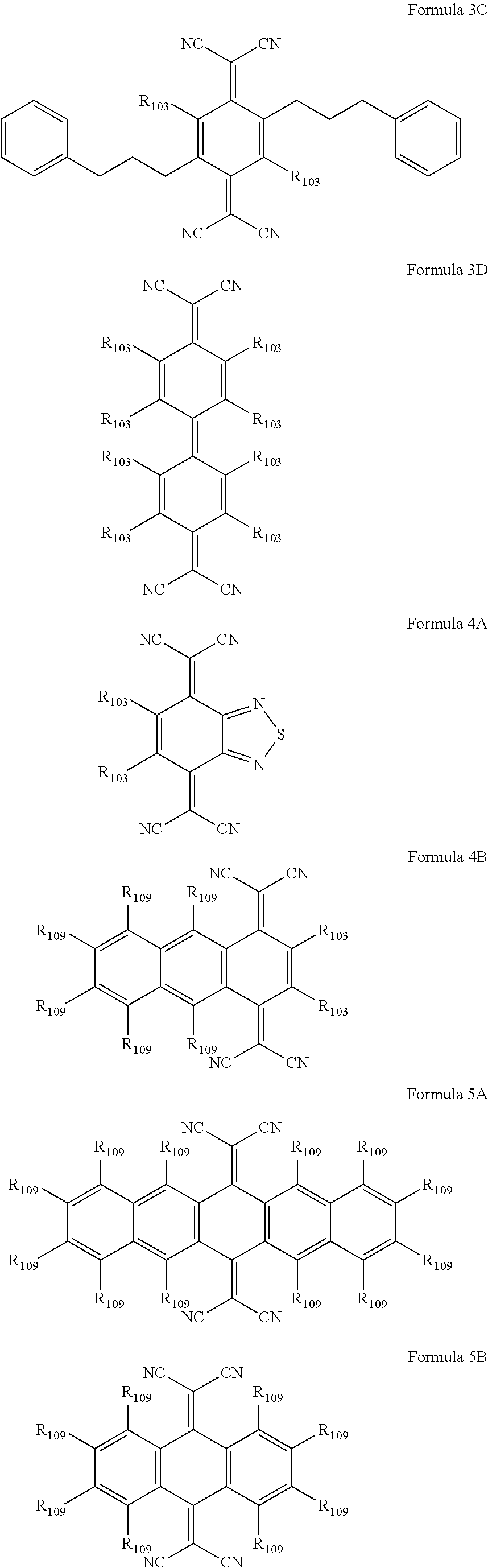
According to an embodiment, the cyano group-containing compound contained in the first layer 6 of the OLED 10 may be represented by one of Formulae 1A through 20B:
##STR00020## ##STR00021## ##STR00022## ##STR00023## ##STR00024## ##STR00025## ##STR00026##
In Formulae 1A through 20B, R.sub.103 and R.sub.109 may each independently be a hydrogen atom, --F, a cyano group, a methyl group, an ethyl group, a propyl group, a methoxy group, an ethoxy group, or a propoxy group.
According to another embodiment, the cyano group-containing compound contained in the first layer 6 of the OLED 10 may be represented by one of Formulae 20A or 20B. In Formulae 20A or 20B, R.sub.103 and R.sub.109 may all be --F.
The first layer 6 may further include, in addition to the cyano group-containing compound described above, a hole transporting compound. The cyano group-containing compound may form a charge transfer complex together with the hole transporting compound, thereby leading to an increase in free carrier concentration. Thus, use of the hole transporting compound may contribute to a decrease in an interface resistance between the first electrode 5 and the organic layer 7.
The hole transporting compound may be any suitable hole transporting materials.
In an implementation, the hole transporting compound may be a compound represented by Formula 41 or 42 below.
##STR00027##
In Formulae 41 and 42, R.sub.10 may be represented by --(Ar.sub.1).sub.n--Ar.sub.2; R.sub.16 may be represented by --(Ar.sub.11).sub.m--Ar.sub.12; Ar.sub.1, Ar.sub.11, L.sub.1 and L.sub.11 may each independently be a substituted or unsubstituted C.sub.1-C.sub.30 alkylene group, a substituted or unsubstituted C.sub.2-C.sub.30 alkenylene group, a substituted or unsubstituted C.sub.5-C.sub.30 arylene group, a substituted or unsubstituted C.sub.4-C.sub.30 heteroarylene group, or a group represented by --N(Q.sub.1)-; n, m, a, and b may each independently be an integer from 0 to 10; R.sub.1 through R.sub.3, R.sub.11 through R.sub.15, R.sub.17, R.sub.13, R.sub.21 through R.sub.29, Ar.sub.2, Ar.sub.12 and Q.sub.1 may each independently be a hydrogen atom, a halogen atom, a hydroxyl group, a cyano group, a substituted or unsubstituted C.sub.1-C.sub.30 alkyl group, a substituted or unsubstituted C.sub.2-C.sub.30 alkenyl group, a substituted or unsubstituted C.sub.2-C.sub.30 alkynyl group, a substituted or unsubstituted C.sub.1-C.sub.30 alkoxy group, a substituted or unsubstituted C.sub.1-C.sub.30 alkylthiol group, a substituted or unsubstituted C.sub.5-C.sub.30 aryl group, a substituted or unsubstituted C.sub.4-C.sub.30 heteroaryl group, or a group represented by --N(Q.sub.2)(Q.sub.3); and Q.sub.2 and Q.sub.3 may each independently be a hydrogen atom, a halogen atom, a hydroxyl group, a cyano group, a substituted or unsubstituted C.sub.1-C.sub.30 alkyl group, a substituted or unsubstituted C.sub.2-C.sub.30 alkenyl group, a substituted or unsubstituted C.sub.2-C.sub.30 alkynyl group, a substituted or unsubstituted C.sub.1-C.sub.30 alkoxy group, a substituted or unsubstituted C.sub.1-C.sub.30 alkylthiol group, a substituted or unsubstituted C.sub.5-C.sub.30 aryl group, or a substituted or unsubstituted C.sub.4-C.sub.30 heteroaryl group, wherein n groups of Ar.sub.1 in --(Ar.sub.1).sub.n may be identical to or different from each other, m groups of Ar.sub.11 in --(Ar.sub.11).sub.m-- may be identical to or different from each other, a groups of L.sub.1 in -(L.sub.1).sub.a- may be identical to or different from each other, and b groups of L.sub.11 in -(L.sub.11).sub.b- may be identical to or different from each other.
Examples of Ar.sub.1 in the formula --(Ar.sub.1).sub.n--Ar.sub.2-- for R.sub.10 and Ar.sub.11 in the formula --(Ar.sub.11).sub.m--Ar.sub.12-- for R.sub.16 may include a substituted or unsubstituted C.sub.1-C.sub.10 alkylene group, a substituted or unsubstituted C.sub.2-C.sub.10 alkenylene group, a substituted or unsubstituted phenylene group, a substituted or unsubstituted pentalenylene group, a substituted or unsubstituted indenylene group, a substituted or unsubstituted naphthylene group, a substituted or unsubstituted azulenylene group, a substituted or unsubstituted heptalenylene group, a substituted or unsubstituted indacenylene group, a substituted or unsubstituted acenaphthylene group, a substituted or unsubstituted fluorenylene group, a substituted or unsubstituted phenalenylene group, a substituted or unsubstituted phenanthrenylene group, a substituted or unsubstituted anthracenylene group, a substituted or unsubstituted fluoranthenylene group, a substituted or unsubstituted triphenylenylene group, a substituted or unsubstituted pyrenylenylene group, a substituted or unsubstituted chrysenylene group, a substituted or unsubstituted naphthacenylene group, a substituted or unsubstituted picenylene group, a substituted or unsubstituted perylenylene group, a substituted or unsubstituted pentaphenylene group, a substituted or unsubstituted hexacenylene group, a substituted or unsubstituted pyrrolylene group, a substituted or unsubstituted pyrazolylene group, a substituted or unsubstituted imidazolylene group, a substituted or unsubstituted imidazolinylene group, a substituted or unsubstituted imidazopyridinylene group, a substituted or unsubstituted imidazopyrimidinylene group, a substituted or unsubstituted pyridinylene group, a substituted or unsubstituted pyrazinylene group, a substituted or unsubstituted pyrimidinylene group, a substituted or unsubstituted indolylene group, a substituted or unsubstituted purinylene group, a substituted or unsubstituted quinolinylene group, a substituted or unsubstituted phthalazinylene group, a substituted or unsubstituted indolizinylene group, a substituted or unsubstituted naphthyridinylene group, a substituted or unsubstituted quinazolinylene group, a substituted or unsubstituted cinnolinylene group, a substituted or unsubstituted indazolylene group, a substituted or unsubstituted carbazolylene group, a substituted or unsubstituted phenazinylene group, a substituted or unsubstituted phenanthridinylene group, a substituted or unsubstituted pyranylene group, a substituted or unsubstituted chromenylene group, a substituted or unsubstituted benzofuranylene group, a substituted or unsubstituted thiophenylene group, a substituted or unsubstituted benzothiophenylene group, a substituted or unsubstituted isothiazolylene group, a substituted or unsubstituted benzoimidazolylene group, a substituted or unsubstituted isoxazolylene group, a substituted or unsubstituted triazinylene group, and a group represented by --N(Q.sub.1)-, but are limited thereto. In this regard, Q.sub.1 may be selected from the group consisting of a hydrogen atom, a halogen atom, a hydroxyl group, a cyano group, a substituted or unsubstituted C.sub.1-C.sub.10 alkyl group, a substituted or unsubstituted C.sub.2-C.sub.10 alkenyl group, a substituted or unsubstituted C.sub.2-C.sub.10 alkynyl group, a substituted or unsubstituted C.sub.1-C.sub.10 alkoxy group, a substituted or unsubstituted C.sub.1-C.sub.10 alkylthiol group, a substituted or unsubstituted C.sub.5-C.sub.14 aryl group, a substituted or unsubstituted C.sub.4-C.sub.14 heteroaryl group, and --N(Q.sub.1)(Q.sub.2)-, but is not limited thereto.
For example, Ar.sub.1 and Ar.sub.11 may each independently be a C.sub.1-C.sub.10 alkylene group; a phenylene group; a naphthylene group; an anthrylene group; a fluorenylene group; a carbazolylene group; a pyrazolylene group; a pyridinylene group; a triazinylene group; --N(Q.sub.1)-; or a C.sub.1-C.sub.10 alkylene group, phenylene group, naphthylene group, anthrylene group, fluorenylene group, carbazolylene group, pyrazolylene group, pyridinylene group, or triazinylene group substituted with at least one of a halogen atom, a cyano group, a hydroxyl group, a C.sub.1-C.sub.10 alkyl group, a C.sub.1-C.sub.10 alkoxy group, a phenyl group, a naphthyl group, and an anthryl group. In this regard, Q.sub.1 may be a hydrogen atom; a C.sub.1-C.sub.10 alkyl group; a C.sub.1-C.sub.10 alkoxy group; a phenyl group; a naphthyl group; a carbazolyl group; a fluorenyl group; a pyrenyl group; a C.sub.1-C.sub.10 alkyl group, C.sub.1-C.sub.10 alkoxy group, phenyl group, naphthyl group, carbazolyl group, fluorenyl group, or pyrenyl group substituted with at least one of a halogen atom, a cyano group, a hydroxyl group, a C.sub.1-C.sub.10 alkyl group, a C.sub.1-C.sub.10 alkoxy group, a phenyl group, a naphthyl group, and an anthryl group; and --N(Q.sub.2)(Q.sub.3). In this regard, each of Q2 and Q3 may be a methyl group, a phenyl group, a naphthyl group, or an anthryl group.
Ar.sub.2 in the formula --(Ar.sub.1).sub.n--Ar.sub.2-- and Ar.sub.12 in the formula --(Ar.sub.11).sub.m--Ar.sub.12-- may be as defined above in connection with Q.sub.1.
n in the formula --(Ar.sub.1)n-Ar.sub.2-- and m in the formula --(Ar.sub.11).sub.m--Ar.sub.12-- may each independently be an integer in the range from 0 to 10. For example, n and m may each independently be 0, 1, 2, 3, 4 or 5, but are not limited thereto.
n groups of Ar.sub.1 in the formula --(Ar.sub.1).sub.n--Ar.sub.2-- may be identical to or different from each other. For example, when n is 2, the two groups of Ar.sub.1 in --(Ar.sub.1).sub.n-- may be both phenylene groups, or one of the two may be --N(Q.sub.1)- and the other may be a phenylene group. This interpretation may also be applied to --(Ar.sub.11).sub.m--Ar.sub.12--.
R.sub.1 through R.sub.3, R.sub.11 through R.sub.15, R.sub.17, R.sub.18, and R.sub.21 through R.sub.29 in 41 and 42 may be defined as described above in connection with Q.sub.1.
For example, R.sub.13 may be a phenyl group, a naphthyl group, or an anthryl group, but is not limited thereto.
For example, R.sub.28 and R.sub.29 may each independently be a hydrogen atom, a methyl group, an ethyl group, a methoxy group, an ethoxy group, a phenyl group, a naphthyl group or an anthryl group, but are not limited thereto.
L.sub.1 and L.sub.2 in Formulae 41 and 42 may be defined as described above in connection with Ar.sub.1 and Ar.sub.11. For example, L.sub.1 and L.sub.2 may each independently be a phenylene group, a C.sub.1-C.sub.10 alkylphenylene group, a fluorophenylene group, a carbazolylene group, a triazinylene group, a C.sub.1-C.sub.10 alkyltriazinylene group, a phenyltriazinylene group, C.sub.1-C.sub.10 alkylene group, or a phenylcarbazolylene group, but are not limited thereto.
In Formulae 41 and 42, a and b may each independently be an integer in the range from 0 to 10. For example, a and b may each independently be 0, 1, 2 or 3, but are not limited thereto.
For example, in Formula 42, Ar.sub.1 in the formula --(Ar.sub.1)n-Ar.sub.2-- for R.sub.10 and Ar.sub.11 in the formula --(Ar.sub.11).sub.m--Ar.sub.12-- for R.sub.16 may each independently be a phenylene group; a carbazolylene group; a fluorenylene group; a methylfluorenylene group; a pyrazolylene group; a phenylpyrazolylene group; --N(Q.sub.1)-, wherein Q.sub.1 is a hydrogen atom, a phenyl group, a fluorenyl group, a dimethylfluorenyl group, a diphenylfluorenyl group, a carbazolyl group, or a phenylcarbazolyl group; a diphenylfluorenylene group; a triazinylene group; a methyltriazinylene group; a phenyltriazinylene group; a tetrafluorophenylene group; an ethylene group; or a methylphenylene group, wherein n and m are each independently 0, 1, 2, 3, 4, 5 or 6, and Ar.sub.2 and Ar.sub.12 are each independently a hydrogen atom, a cyano group, a fluoro group, a phenyl group, a cyanophenyl group, a naphthyl group, an anthryl group, a methyl group, a pyridinyl group, a carbazolyl group, a phenylcarbazolyl group, a fluorenyl group, a dimethylfluorenyl group, and a diphenylfluorenyl group. In Formula 42, R.sub.11, R.sub.12, R.sub.14, R.sub.15, R.sub.17, R.sub.18, R.sub.21 through R.sub.27 may be a hydrogen atom; R.sub.13 may be a phenyl group, a naphthyl group or an anthryl group; R.sub.28 and R.sub.29 may each independently be a hydrogen atom, a methyl group, an ethyl group, a methoxy group, an ethoxy group, a phenyl group, a naphthyl group, or an anthryl group; L.sub.11 may be a phenylene group; and b may be 0 or 1.
For example, in Formula 42, R.sub.13 may be represented by one of Formulae 101A to 101D.
##STR00028##
For example, in Formula 42, L.sub.11 may be a phenylene group and b may be 1. For example, in Formula 42, R.sub.10 may be represented by one of Formulae 102A to 102G.
##STR00029##
For example, in Formula 42, R.sub.28 and R.sub.29 may each independently be a methyl group or a phenyl group. For example, in Formula 42, R.sub.11, R.sub.12, R.sub.14 to R.sub.18 and R.sub.21 to R.sub.27 may be a hydrogen atom.
For example, in Formula 41, R.sub.1, R.sub.2, and R.sub.3 may each independently be a C.sub.1-C.sub.10 alkyl group; a C.sub.1-C.sub.10 alkoxy group; a phenyl group; a naphthyl group; a carbazolyl group; a fluorenyl group; a pyrenyl group; an anthryl group; a pyrazolyl group; a pyridinyl group; a C.sub.1-C.sub.10 alkyl group, a C.sub.1-C.sub.10 alkoxy group, a phenyl group, a naphthyl group, a carbazolyl group, a fluorenyl group, a pyrenyl group, an anthryl group, a pyrazolyl group or a pyridinyl group substituted with at least one of a halogen atom, a cyano group, a hydroxyl group, a C.sub.1-C.sub.10 alkyl group, a C.sub.1-C10 alkoxy group, a phenyl group, a cyanophenyl group, a diphenylamino group, a naphthyl group, a carbazolyl group, a fluorenyl group, a C.sub.1-C.sub.10 alkyfluorenyl group, a di(C.sub.1-C.sub.10 alky)fluorenyl group, a phenylfluorenyl group, a di(phenyl)fluorenyl group, and an anthryl group; or --N(Q2)(Q3). In this regard, each of Q2 and Q3 may each independently be a C.sub.1-C.sub.10 alkyl group; a C.sub.1-C.sub.10 alkoxy group; a phenyl group; a naphthyl group; a carbazolyl group; a fluorenyl group; a pyrenyl group; an anthryl group; a pyrazolyl group; a pyridinyl group; or a C.sub.1-C.sub.10 alkyl group, a C.sub.1-C.sub.10 alkoxy group, a phenyl group, a naphthyl group, a carbazolyl group, a fluorenyl group, a pyrenyl group, an anthryl group, a pyrazolyl group or a pyridinyl group substituted with at least one of a halogen atom, a cyano group, a hydroxyl group, a C.sub.1-C.sub.10 alkyl group, a C.sub.1-C.sub.10 alkoxy group, a phenyl group, a cyanophenyl group, a diphenylamino group, a naphthyl group, a carbazolyl group, a fluorenyl group, a C.sub.1-C.sub.10 alkyfluorenyl group, a di(C.sub.1-C.sub.10 alky)fluorenyl group, a phenylfluorenyl group, a di(phenyl)fluorenyl group, and an anthryl group.
For example, in Formula 41, R.sub.1, R.sub.2, and R.sub.3 may each independently be one of Formulae 201 to 226 as follows:
##STR00030## ##STR00031## ##STR00032## ##STR00033## ##STR00034##
In an implementation, the hole transporting material may be any one of compounds represented by Compounds 1 through 38 below, but is not limited thereto:
##STR00035## ##STR00036## ##STR00037## ##STR00038## ##STR00039## ##STR00040## ##STR00041## ##STR00042##
When the first layer 6 further includes, in addition to the cyano group-containing compound, the hole transporting compound described above, an amount of the cyano group-containing compound included in the first layer 6 may be about 0.1 parts by weight to about 20 parts by weight, or about 0.5 parts by weight to about 10 parts by weight, or about 0.5 parts by weight to about 5 parts by weight, based on 100 parts by weight of the first layer. Maintaining the amount of the cyano group-containing compound at about 0.1 parts by weight to about 20 parts by weight may help ensure that satisfactory driving voltage decrease and power efficiency increase effects may be obtained.
A thickness of the first layer 6 may be about 10 .ANG. to about 2,100 .ANG., or about 10 .ANG. to about 500 .ANG., or about 20 .ANG. to about 200 .uparw.. Maintaining the thickness of the first layer 6 is at about 10 .ANG. to about 2,100 .ANG. may help ensure that satisfactory driving voltage decrease and power efficiency increase effects may be obtained.
The organic layer 7 may be disposed on the first electrode 6. The term "organic layer" used throughout the specification refers to any intervening layer between the first electrode 5 and the second electrode 9 (although the first layer 6 described above is excluded herein). The organic layer 7 may not be formed of pure organic materials, and may include, e.g., a metal complex.
The organic layer 7 may include an emission layer (EML).
A distance between the first layer 6 and the EML may be about 50 .ANG. or more, or about 100 .ANG. or more, or about 100 .ANG. to about 1,400 .ANG.. Maintaining the distance between the first layer 6 and the EML at about 50 .ANG. or more may help ensure that excitons contained in the EML are not substantially quenched by the cyano group-containing compound contained in the first layer 6, and thus an OLED having excellent qualities may be obtained.
The organic layer 7 may further include, in addition to the EML, at least one of a hole injection layer (HIL), a hole transport layer (HTL), a hole blocking layer (HBL), an electron transport layer (ETL), and an electron injection layer (EIL).
For example, at least one of a HIL and a HTL may be further interposed between the first layer 6 and the EML. For example, a HTL may be further interposed between the first layer 6 and the EML.
The HIL may be formed on the first layer 6 by, e.g., vacuum deposition, spin coating, casting, LB deposition, or the like.
When the HIL is formed using vacuum deposition, the deposition conditions may vary according to a compound that is used to form the HIL and structure and thermal properties of the HIL to be formed. In general, however, conditions for vacuum deposition may include a deposition temperature of about 100 to about 500.degree. C., a vacuum pressure of about 10.sup.-8 to about 10.sup.-3 torr, and a deposition rate of about 0.01 to about 100 .ANG./sec.
When the HIL is formed using spin coating, the coating conditions may vary according to a compound that is used to form the HIL, and the structure and thermal properties of the HIL to be formed. In general, however, conditions for spin coating may include a coating rate of about 2,000 to about 5,000 rpm and a heat treatment temperature of about 80 to about 200.degree. C., wherein the heat treatment is performed to remove a solvent after coating.
The HIL may be formed of any suitable material that is commonly used to form a HIL. Examples of the material that can be used to form the HIL may include a phthalocyanine compound such as copperphthalocyanine, 4,4',4''-tris(3-methylphenylphenylamino)triphenylamine (m-MTDATA), N,N'-di(1-naphthyl)-N,N'-diphenylbenzidine (NPB), TDATA, 2T-NATA, polyaniline/dodecylbenzenesulfonic acid (Pani/DBSA), poly(3,4-ethylenedioxythiophene)/poly(4-styrenesulfonate) (PEDOT/PSS), polyaniline/camphor sulfonicacid (Pani/CSA), and polyaniline)/poly(4-styrenesulfonate (PANI/PSS), but are not limited thereto.
##STR00043##
The HIL may have a thickness of about 50 .ANG. to about 10,000 .ANG., for example, a thickness of about 100 .ANG. to about 2,500 .ANG.. Maintaining the thickness of the HIL at about 50 .ANG. to about 10,000 .ANG. may help ensure that the HIL has an excellent hole injecting ability without a substantial increase in driving voltage.
Then, a HTL may be formed on the HIL or the first layer 6 by using, e.g., vacuum deposition, spin coating, casting, Langmuir-Blodgett (LB) deposition, or the like. When the HTL is formed by vacuum deposition or spin coating, the conditions for deposition and coating may be similar to those for the formation of the HIL, although the conditions for the deposition and coating may vary according to the material that is used to form the HTL.
The HTL may be formed of the compound represented by Formula 41 or 42 described above.
The HTL may have a thickness of about 50 .ANG. to about 10,000 .ANG., for example, a thickness of 100 .ANG. to about 2,500 .ANG.. Maintaining the thickness of the HTL at about 50 .ANG. to about 10,000 .ANG. may help ensure that an excellent hole transporting ability of the HTL is obtained without a substantial increase in driving voltage.
Then, an EML may be formed on the HTL by using, e.g., vacuum deposition, spin coating, casting, LB deposition, or the like. When the EML is formed using vacuum deposition or spin coating, the conditions for deposition and coating may be similar to those for the formation of the HIL, although the conditions for deposition and coating may vary according to the material that is used to form the EML.
The EML may include a compound, or a combination of a host and a dopant. Examples of the host material may include Alq.sub.3, 4,4'-N,N'-dicarbazole-biphenyl (CBP), TCTA, 1,3,5-tris(N-phenylbenzimidazole-2-yl)benzene) (TPBI), E3, distyrylarylene (DSA), a compound represented by Formula 51, a compound represented by Formula 52, a compound represented by Formula 53, or a compound represented by Formula 54, but are not limited to.
##STR00044## ##STR00045##
In Formulae 51 through 54 above, Ar.sub.51, A.sub.52, Ar.sub.53 and Ar.sub.54 may be defined as described above in connection with Ar.sub.1.
In Formulae 51 through 54, Ar.sub.51, A.sub.52, Ar.sub.53 and Ar.sub.54 may each independently be a phenylene group, a naphthylene group, an anthrylene group, or a phenyl-substituted anthrylene group, but are not limited thereto.
In Formulae 51 through 54, R.sub.201 through R.sub.209 and R.sub.51 through R.sub.56 may be defined as described above in connection with Ar.sub.2. For example, R.sub.201 through R.sub.209 may be hydrogen.
In Formulae 51 through 54, d, e, f and g may each independently be an integer from 0 to 10. For example, d, e, f, and g may each independently be 0, 1, or 2, but are not limited thereto.
In Formulae 51 through 54, R.sub.51 through R.sub.56 may each independently be a hydrogen atom, a methyl group, an ethyl group, a propyl group, a butyl group, a phenyl group, a naphthyl group, an anthryl group, a pyrenyl group, a carbazolyl group, or --N(Q.sub.2)(Q.sub.3), wherein Q.sub.2 and Q.sub.3 are each independently a methyl group, a phenyl group, a naphthyl group, or an anthryl group.
In an implementation, the EML of the organic layer 7 may include one compound represented by Compounds 51 through 58 as a host, but is not limited thereto.
##STR00046## ##STR00047##
Examples of red dopants may include PtOEP, Ir(piq).sub.3, and Btp.sub.2Ir(acac), but are not limited thereto.
##STR00048##
Examples of green dopants may include Ir(ppy).sub.3 (ppy=phenylpyridine), Ir(ppy).sub.2(acac), and Ir(mpyp).sub.3, a compound represented by any one of Formulae 51 through 54, a compound represented by Formula 71 below, and a compound represented by Formula 72, but are not limited thereto.
##STR00049##
In Formulae 71 and 72, Ar.sub.71 and Ar.sub.72 may be defined as described above in connection with Ar.sub.1.
In Formulae 71 and 72, Ar.sub.71 and Ar.sub.72 may each independently be an ethenylene group, a phenylene group, a naphthylene group, an anthrylene group, or a phenyl-substituted anthrylene group, but are not limited thereto.
In Formulae 71 and 72, R.sub.211 through R.sub.216 and R.sub.71 through R.sub.76 may be defined as described above in connection with Ar.sub.2. For example, R.sub.211 through R.sub.216 may be hydrogen.
In Formula 71 and 72, h and i may each independently be an integer from 0 to 10. For example, h and i may be each independently 0, 1 or 2.
In Formulae 71 and 72, R.sub.71 through R.sub.76 may each independently be a methyl group, an ethyl group, an ethenyl group, a phenyl group, a methylphenyl group, a naphthyl group, a methylnaphthyl group, an anthryl group, a methylanthryl group, a pyrenyl group, or --N(Q.sub.2)(Q.sub.3), wherein Q.sub.2 and Q.sub.3 are each independently a methyl group, a phenyl group, a naphthyl group, or an anthryl group.
In another implementation, the EML may include one compound represented by Compounds 51 through 58 above, and Compounds 71 through 76 below, as a green dopant, but is not limited thereto.
##STR00050## ##STR00051##
Examples of blue dopants may include F.sub.2Irpic, (F.sub.2ppy).sub.2Ir(tmd), Ir(dfppz).sub.3, ter-fluorene, 4,4'-bis(4-diphenyl amiostyryl)biphenyl (DPAVBi), 2,5,8,11-tetra-tert-butyl perylene (TBPe), compounds represented by Formulae 51, 54, 81, and 82, but are not limited thereto.
##STR00052## ##STR00053##
In Formula 81, L.sub.21 may be a substituted or unsubstituted C.sub.1-C.sub.30 alkylene group, a substituted or unsubstituted C.sub.2-C.sub.30 alkenylene group, a substituted or unsubstituted C.sub.5-C.sub.30 arylene group, or a substituted or unsubstituted C.sub.4-C.sub.30 heteroarylene group; c may be an integer from 1 to 20; c groups of L.sub.21 in -(L.sub.21).sub.c- may be identical to or different from each other; R.sub.31 through R.sub.34 may each independently be a substituted or unsubstituted C.sub.1-C.sub.30 alkyl group, a substituted or unsubstituted C.sub.2-C.sub.30 alkenyl group, a substituted or unsubstituted C.sub.2-C.sub.30 alkynyl group, a substituted or unsubstituted C.sub.1-C.sub.30 alkoxy group, a substituted or unsubstituted C.sub.5-C.sub.30 aryl group, or a substituted or unsubstituted C.sub.4-C.sub.30 heteroaryl group.
In Formula 81, L.sub.21 may be defined as described above in connection with Ar.sub.1 (the description of --N(Q.sub.1)- is excluded), and R.sub.31 through R.sub.34 may be defined as described above in connection with Q.sub.1 (the description of --N(Q.sub.2)(Q.sub.3) is excluded).
In an example of Formula 81, L.sub.21 may be an ethenylene group, a prophenylene group, or a phenylene group.
In anther example of Formula 81, c may be 1, 2, 3, 4, 5, or 6.
In another example of Formula 81, R.sub.31 through R.sub.34 may each independently be a hydrogen atom, a methyl group, an ethyl group, a propyl group, a butyl group, a methoxy group, an ethoxy group, a propoxy group, a butoxy group, a phenyl group, a naphthyl group, or an anthryl group.
In Formula 81, c groups of L.sub.21 in -(L.sub.21).sub.c- may be identical to or different from each other. For example, when c is 2, the two groups of L.sub.21 may be both phenylene groups, or one of the two may be a phenylene group, and the other may be an ethenylene group.
In Formula 82, Ar.sub.81 and Ar.sub.84 may be defined as described above in connection with Ar1.
In Formula 82, Ar.sub.31, A.sub.32, Ar.sub.33 and Ar.sub.34 may each independently be a phenylene group, a naphthylene group, an anthrylene group, or a phenyl-substituted anthrylene group, but are not limited thereto.
In Formula 82, R.sub.221 through R.sub.228 and R.sub.81 through R.sub.85 may be defined as described above in connection with Ar.sub.2. For example, R.sub.221 through R.sub.228 may be hydrogen.
In Formula 82, j, k, l, and m may each independently be an integer from 0 to 10. For example, j, k, l, and m may each independently be 0, 1, or 2.
In Formula 82, R.sub.81 through R.sub.85 may each independently be a hydrogen atom, a methyl group, an ethyl group, a propyl group, a butyl group, a phenyl group, a naphthyl group, an anthryl group, a pyrenyl group, a carbazolyl group, or --N(Q.sub.2)(Q.sub.3), wherein Q.sub.2 and Q.sub.3 are each independently a methyl group, a phenyl group, a naphthyl group, or an anthryl group.
The compound of Formula 81 may be Compound 40 below, but is not limited thereto:
##STR00054##
The compound of Formula 82 may be represented by Compound 41 or 42 below, but is not limited thereto:
##STR00055##
In an implementation, the EML may include any one of Compounds 40 through 42, 51 through 55, 57, and 58, as a blue dopant, but is not limited thereto.
When a dopant and a host are used together as materials for the EML, the amount of the dopant may be in a range of about 0.01 to about 15 parts by weight based on 100 parts by weight of the host, but is not limited thereto.
The EML may have a thickness of about 100 .ANG. to about 1,000 .ANG., for example, about 200 .ANG. to about 600 .ANG.. Maintaining the thickness of the EML at about 100 .ANG. to about 1,000 .ANG. may help ensure that the EML has excellent emitting ability without a substantial increase in driving voltage.
When a phosphorescent dopant is also used to form the EML, a HBL may be formed between the HTL and the EML by using, e.g., vacuum deposition, spin coating, casting, LB deposition, or the like, in order to prevent diffusion of triplet excitons or holes into an ETL. When the HBL is formed using vacuum deposition or spin coating, the conditions for deposition and coating may be similar to those for the formation of the HIL, although the conditions for deposition and coating may vary according to the material that is used to form the HBL. Any suitable material that is commonly used to form a HBL may be used. Examples of materials for forming the HBL may include an oxadiazole derivative, a triazole derivative, and a phenanthroline derivative, but are not limited thereto.
The HBL may have a thickness of about 50 .ANG. to about 1,000 .ANG., for example, about 100 .ANG. to about 400 .ANG.. Maintaining the thickness of the HBL at about 50 .ANG. to about 1,000 .ANG. may help ensure that the HBL has an excellent hole blocking ability without a substantial increase in driving voltage.
Then, an ETL may be formed on the HBL or EML by, e.g., vacuum deposition, spin coating, casting, or the like. When the ETL is formed using vacuum deposition or spin coating, the deposition and coating conditions may be similar to those for formation of the HIL, although the deposition and coating conditions may vary according to a compound that is used to form the ETL. A material for forming the ETL may be any suitable material that can stably transport electrons injected from an electron injecting electrode (cathode). Examples of materials for forming the ETL may include a quinoline derivative, such as tris(8-quinolinorate)aluminum (Alq.sub.3), TAZ, and Balq, but are not limited thereto.
##STR00056##
The ETL may have a thickness of about 100 .ANG. to about 1,000 .ANG., for example, about 150 .ANG. to about 500 .ANG.. Maintaining the thickness of the ETL at about 100 .ANG. to about 1,000 .ANG. may help ensure that the ETL has satisfactory electron transporting ability without a substantial increase in driving voltage.
Then, an EIL may be formed on the ETL. The EIL may be formed of any suitable material allowing electrons to be easily injected from the cathode.
Examples of materials for forming the EIL may include LiF, NaCl, a CsF, Li.sub.2O, and BaO, which are known in the art. Deposition and coating conditions for forming the EIL are similar to those for formation of the HIL, although the deposition and coating conditions may vary according to a material that is used to form the EIL.
The EIL may have a thickness of about 1 .ANG. to 100 .ANG., for example, about 5 .ANG. to about 90 .ANG.. Maintaining the thickness of the EIL at about 1 .ANG. to 100 .ANG. may help ensure that the EIL has satisfactory electron injecting properties without a substantial increase in a driving voltage of the organic light emitting diode.
Finally, the second electrode 9 is formed on the organic layer 7. The second electrode 9 may be a cathode, which is an electron injecting electrode. A material for forming the second electrode 9 may include, e.g., a metal, an alloy, an electrically conductive compound, which have a low-work function, or a mixture thereof. In this regard, the second electrode 9 may be formed of, e.g., lithium (Li), magnesium (Mg), aluminum (Al), aluminum (Al)-lithium (Li), calcium (Ca), magnesium (Mg)-indium (In), magnesium (Mg)-silver (Ag), or the like, and may be formed as a thin film type transmission electrode. In addition, the transmission electrode may be formed of ITO or IZO to manufacture a top-emission type light-emitting device.
For example, the OLED may include an Al-based reflective layer formed of Al, Ni, and La; a transparent conductive layer formed of ITO; a first layer containing a cyano group-containing compound represented by any one of Formulae 1A through 20B (herein, the first layer may further, optionally include the hole transporting compound represented by Formula 42); a HTL including the compound represented by Formula 42; an EML including a host (a compound represented by any one of Formulae 51 through 54) and a dopant (a compound represented by any one of Formulae 51 through 54, 71, and 72); an ETL; an EIL; and a second electrode, which are sequentially stacked in this order, and may emit green light having high quality. The green light may be emitted according to a fluorescent light emission mechanism. A maximum emission peak wavelength of the green light may be about 490 to about 560 nm.
Alternatively, for example, the OLED may include an Al-based reflective layer formed of Al, Ni, and La; a transparent conductive layer formed of ITO; a first layer containing a cyano group-containing compound represented by any one of Formulae 20A and 20B (herein, the first layer may further, optionally include any one of Compounds 1 through 37 being the hole transporting compound); a HTL including any one of Compounds 1 through 37; an EML including a host (any one of Compounds 51 through 58) and a dopant(any one of Compounds 40 through 42 and 51 through 58); an ETL; an EIL; and a second electrode, which are sequentially stacked in this order, and may emit green light having high quality.
FIG. 4 illustrates a schematic sectional view of an OLED 30 according to another embodiment. Referring to FIG. 4, the OLED 30 according to the present embodiment may include, e.g., a substrate 21, a first electrode 25, a first layer 26 containing a cyano group-containing compound, an organic layer 27, and a second electrode 29, wherein the second electrode 25 includes an Al-based reflective layer 25a including nickel (Ni) and a first element, a transparent conductive layer 25b, and a second element-containing zinc oxide layer 25c, which are disposed in this order on the substrate 21. The substrate 21, the first layer 26 containing a cyano group-containing compound, the organic layer 27, the second electrode 29, the Al-based reflective layer 25a including Ni and the first element, and the transparent conductive layer 25b are the same as described above with reference to FIG. 1, and thus the above description may be referred to.
Referring to FIG. 4, in the OLED 30 according to the present embodiment, the first electrode 25 may further include a second element-containing zinc oxide layer 25c, compared to the OLED 10 in FIG. 1. The second element-containing zinc oxide layer 25c may lower a hole injection barrier by increasing the work function of the first electrode 25, and thus, may allow holes to be easily injected into the organic layer 27 from the first electrode 25.
In this regard, in the first layer 26 containing a cyano group-containing compound, the cyano group-containing compound may further enhance hole injecting characteristics of the second element-containing zinc oxide layer 25c. Thus, an OLED having lower driving voltage and better power efficiency characteristics may be obtained.
The second element in the second element-containing zinc oxide layer 25c may include at least one of aluminum (Al), indium (In), gallium (Ga), germanium (Ge), gadolinium (Gd), zirconium (Zr), molybdenum (Mo), and nickel (Ni). For example, the second element may include aluminum (Al). The second element may be aluminum (Al), but is not limited thereto.
The second element may be included in the second element-containing zinc oxide layer 25c in an amount of about 0.5 parts by weight to about 10 parts by weight, based on 100 parts by weight of the second element-containing zinc oxide layer 25c. Maintaining the amount of the second element in the second element-containing zinc oxide layer 25c at about 0.5 parts by weight to about 10 parts by weight may help ensure that the second element-containing zinc oxide layer 25c has excellent hole transporting ability without a substantial increase in electrical resistance or a substantial reduction in the transmittance of visible light. For example, the amount of the second element may be about 0.5 to about 5 parts by weight, based on 100 parts by weight of the second element-containing zinc oxide layer 25c, but is not limited thereto.
The second element-containing zinc oxide layer 25c may have a thickness of about 1 .ANG. to about 800 .ANG., for example, about 10 .ANG. to 500 .ANG.. Maintaining the thickness of the second element-containing zinc oxide layer 25c at about 1 .ANG. to about 800 .ANG. may help ensure that excellent efficiency characteristics are attained without a substantial increase in driving voltage.
For example, the OLED may include an Al-based reflective layer formed of Al, Ni, and La; a transparent conductive layer formed of ITO; an Al-containing zinc oxide layer; a first layer containing a cyano group-containing compound represented by any one of Formulae 1A through 20B (herein, the first layer may further, optionally include the hole transporting compound represented by Formula 42); a HTL including the compound represented by Formula 42; an EML including a host (a compound represented by any one of Formulae 51 through 54) and a dopant (a compound represented by any one of Formulae 51 through 54, and 72); an ETL; an EIL; and a second electrode, which are sequentially stacked in this order, and may emit green light having high quality. The green light may be emitted according to a fluorescent light emission mechanism. The maximum emission peak wavelength of the green light may be about 490 to about 560 nm.
Alternatively, for example, the OLED may include an Al-based reflective layer formed of Al, Ni and La; a transparent conductive layer formed of ITO; an Al-containing zinc oxide layer; a first layer containing a cyano group-containing compound represented by any one of Formulae 20A and 20B (herein, the first layer may further, optionally include any one of Compounds 1 through 37 being the hole transporting compound); a HTL including any one of Compounds 1 through 37; an EML including a host (any one of Compounds 51 through 58) and a dopant(any one of Compounds 40 through 42 and 51 through 58); an ETL; an EIL; and a second electrode, which are sequentially stacked in this order, and may emit green light having high quality.
The OLEDs 10 and 30 according to the embodiments are illustrated in FIGS. 1 and 4. However, the embodiments are not limited thereto.
For example, any of the OLEDs 10 and 30 may further include a metal layer between the Al-based reflective layer 5a (25a) and the substrate 1 (21). The metal layer may function as a barrier layer that blocks diffusion of Al in the Al-based reflective layer 5a (25a) into the substrate 1 (21). The metal layer may include at least one of molybdenum (Mo), tungsten (W), titanium (Ti), palladium (Pd), platinum (Pt), and gold (Au), but is not limited thereto. For example, the metal layer may include a titanium (Ti) layer. The metal layer may have a thickness of about 20 nm to about 200 nm, for example, about 50 nm to about 100 nm. Maintaining the thickness of the metal layer at about 20 nm to about 200 nm may help ensure that diffusion of aluminum (Al) may be effectively prevented. However, the thickness of the metal layer is not limited thereto.
The OLED may include at least one of a HIL and a HTL between the first electrode and the first layer. That is, for example, the OLED may include a substrate, a first electrode, a first HTL, a first layer, a second HTL, an EML, an ETL, an EIL, and a second electrode, which are sequentially stacked in this order.
Hereinafter, one or more embodiments will be described in detail with reference to the following examples. However, these examples are not intended to limit the purpose and scope of the one or more embodiments.
EXAMPLES
Comparative Example 1
A 15 .OMEGA./cm.sup.2 (1200 .ANG.) ITO glass substrate (available from Corning Co.) was cut to a size of 50 mm.times.50 mm.times.0.7 mm, ultrasonically washed with isopropyl alcohol for 5 minutes and then washed with pure water for 5 minutes, and washed again with UV ozone for 30 minutes. The resultant ITO glass substrate was used as a substrate and an anode. Then, m-MTDATA was vacuum-deposited on the resultant ITO glass substrate to form a HIL having a thickness of 750 .ANG., and then Compound 5 above was vacuum-deposited on the HIL to form a HTL having a thickness of 750 .ANG.. 97 wt % of Compound 56 above as a host and 3 wt % of Compound 58 above as a dopant were deposited on the HTL to form an EML having a thickness of 200 .ANG.. Alq3 was vacuum-deposited on the EML to form an ETL having a thickness of 300 .ANG.. Liq was vacuum-deposited on the ETL to form an EIL having a thickness of 5 .ANG. and Mg and Al were vacuum-deposited on the EIL to form a cathode having a thickness of 160 .ANG.. Next, Alq3 was deposited on the cathode to form a protection layer having a thickness of 600 .ANG., thereby completing the manufacture of an OLED.
Example 1
An OLED was manufactured in the same manner as in Comparative Example 1, except that as a substrate and an anode, a glass substrate on which an AlNiLa layer having a thickness of 5000 .ANG. (in the AlNiLa layer, the amount of nickel (Ni) was 2 wt %, and the amount of lanthanum (La) was 0.3 wt %), an ITO layer having a thickness of 70 .ANG. as a transparent conductive layer, and an Al-containing zinc oxide layer having a thickness of 400 .ANG. (the concentration of Al was 2 parts by weight based on 100 parts by weight of the Al-containing zinc oxide layer) were sequentially formed in this order, was used instead of the ITO glass substrate; and a first layer including the compound represented by Formula 20A (where R.sub.109 is --F) and Compound 14 was formed instead of the HIL on the Al-containing zinc oxide layer and then the HTL was formed, wherein the amount of the compound represented by Formula 20A was 1 part by weight based on 100 parts by weight of the first layer.
Example 2
An OLED was manufactured in the same manner as in Example 1, except that the amount of the compound represented by Formula 20A was 3 parts by weight based on 100 parts by weight of the first layer.
Evaluation
Driving voltages of the OLEDs manufactured in Comparative Example 1 and Examples 1 and 2 was measured using a 238 High Current Source (KEITHLEY). Power efficiency of the OLEDs manufactured in Comparative Example 1 and Examples 1 through 2 was measured using a PR650 Spectroscan Source Measurement Unit (PhotoResearch). The results are shown in Table 1 below.
TABLE-US-00001 TABLE 1 Power efficiency (Im/W) Driving voltage (V) Comparative 14.5 5.1 Example 1 Example 1 18.6 4.5 Example 2 16.3 4.6
Referring to Table 1, it may be confirmed that the OLEDS of Examples 1 through 2 exhibited lower driving voltages and higher power efficiencies than the OLED of Comparative Example 1.
As described above, an OLED according to an embodiment may have excellent driving voltage characteristics and excellent power efficiency characteristics.
Exemplary embodiments have been disclosed herein, and although specific terms are employed, they are used and are to be interpreted in a generic and descriptive sense only and not for purpose of limitation. Accordingly, it will be understood by those of ordinary skill in the art that various changes in form and details may be made without departing from the spirit and scope of the present invention as set forth in the following claims.
* * * * *
C00001
C00002
C00003
C00004
C00005
C00006
C00007
C00008
C00009
C00010
C00011
C00012
C00013

C00014

C00015

C00016

C00017

C00018
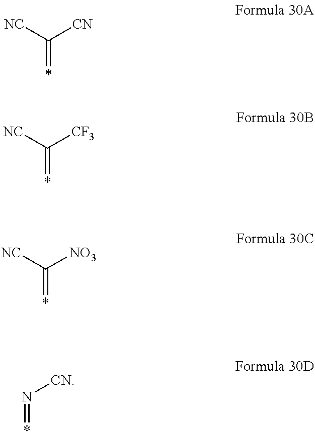
C00019

C00020

C00021
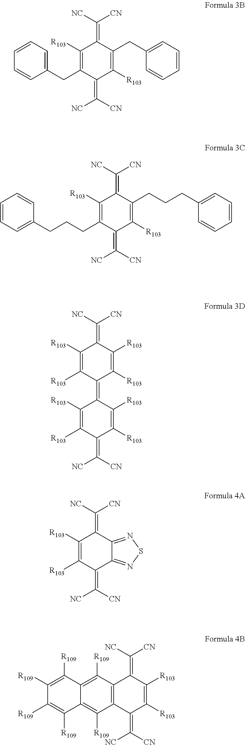
C00022

C00023

C00024
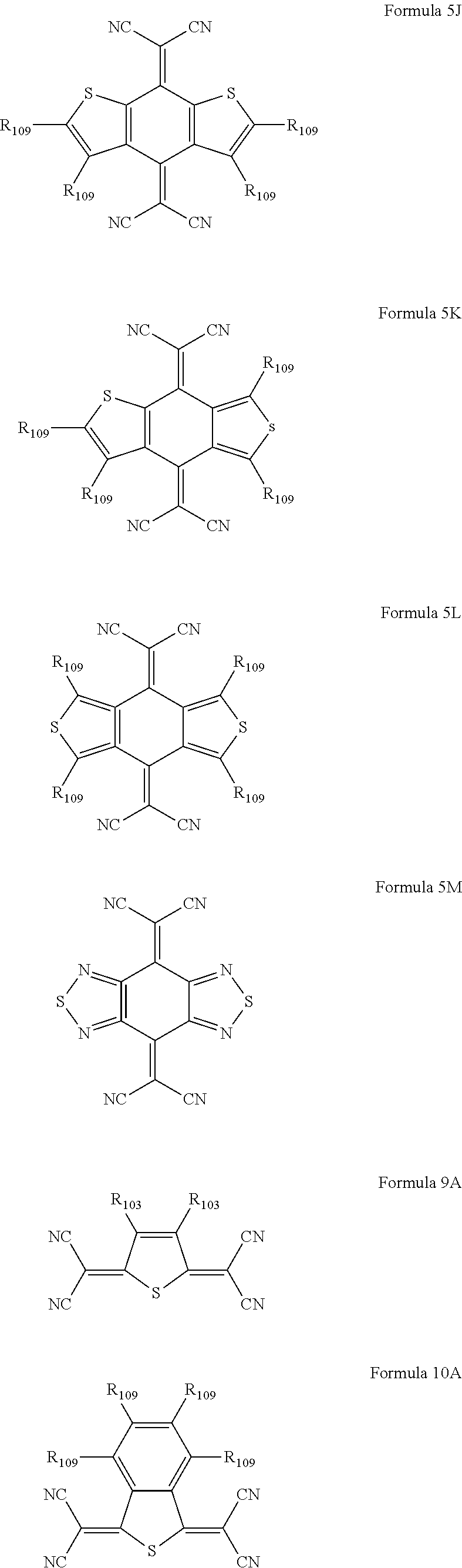
C00025

C00026

C00027

C00028
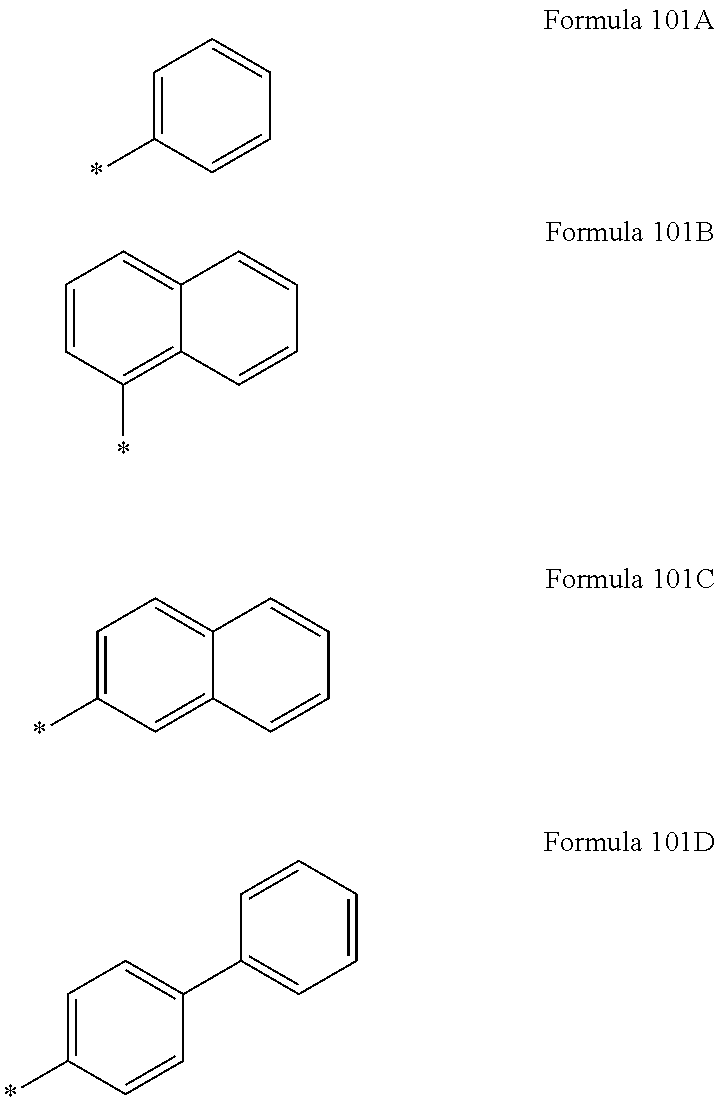
C00029

C00030

C00031

C00032

C00033

C00034

C00035
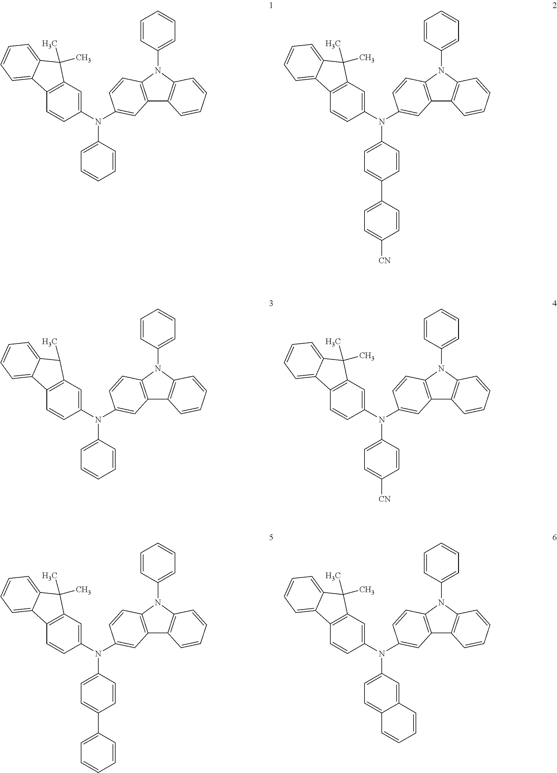
C00036
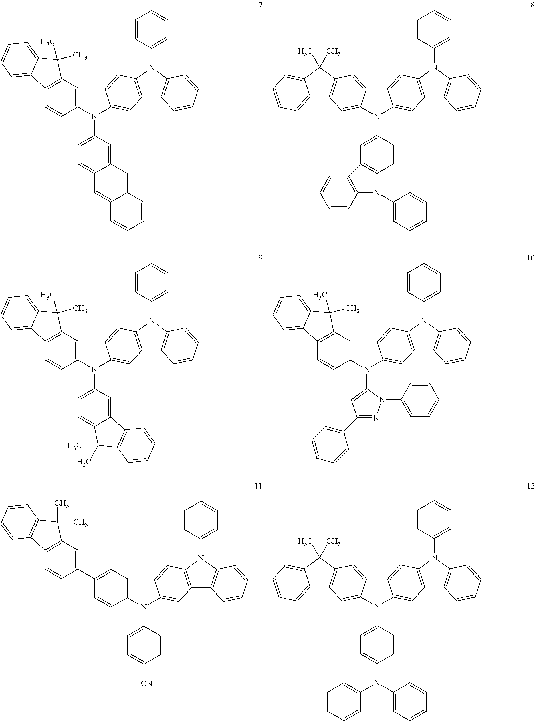
C00037

C00038

C00039
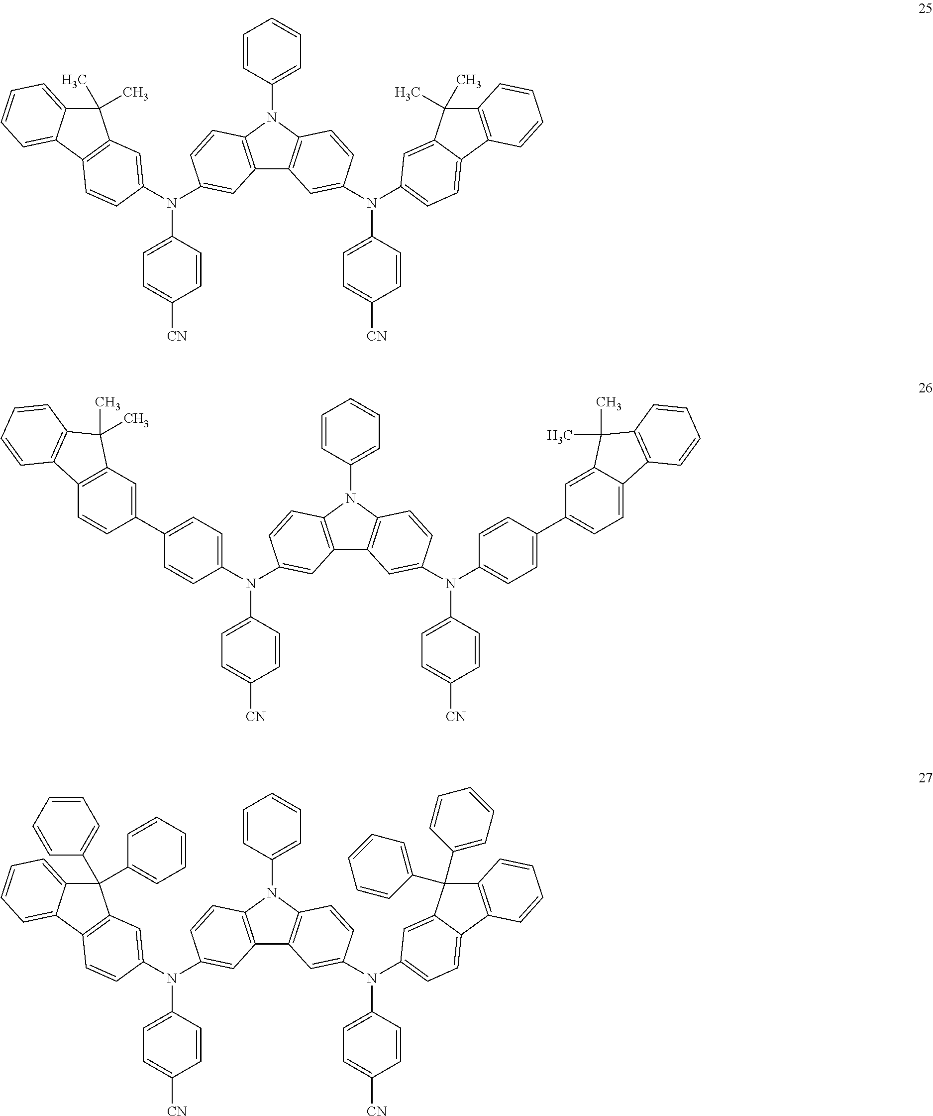
C00040
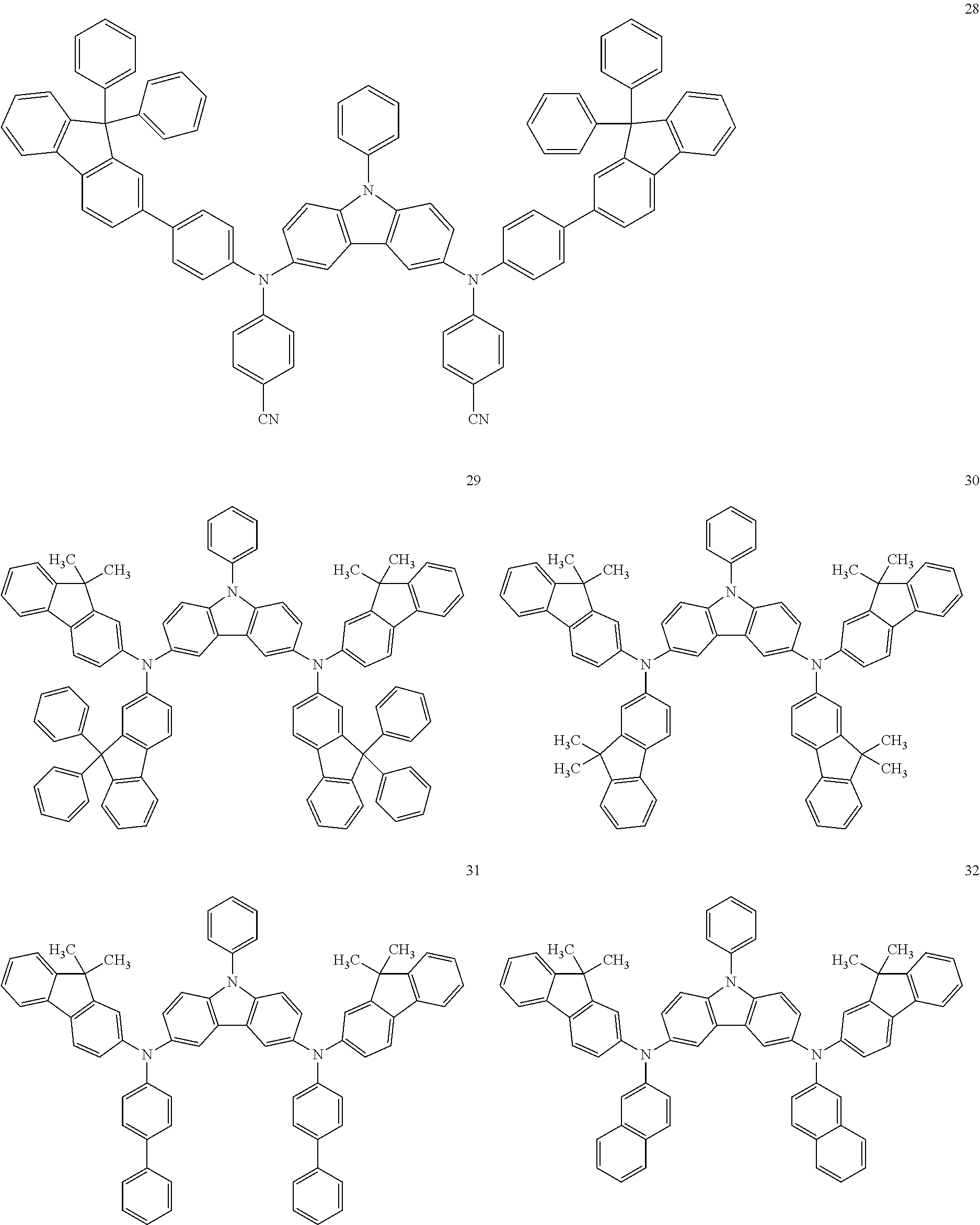
C00041
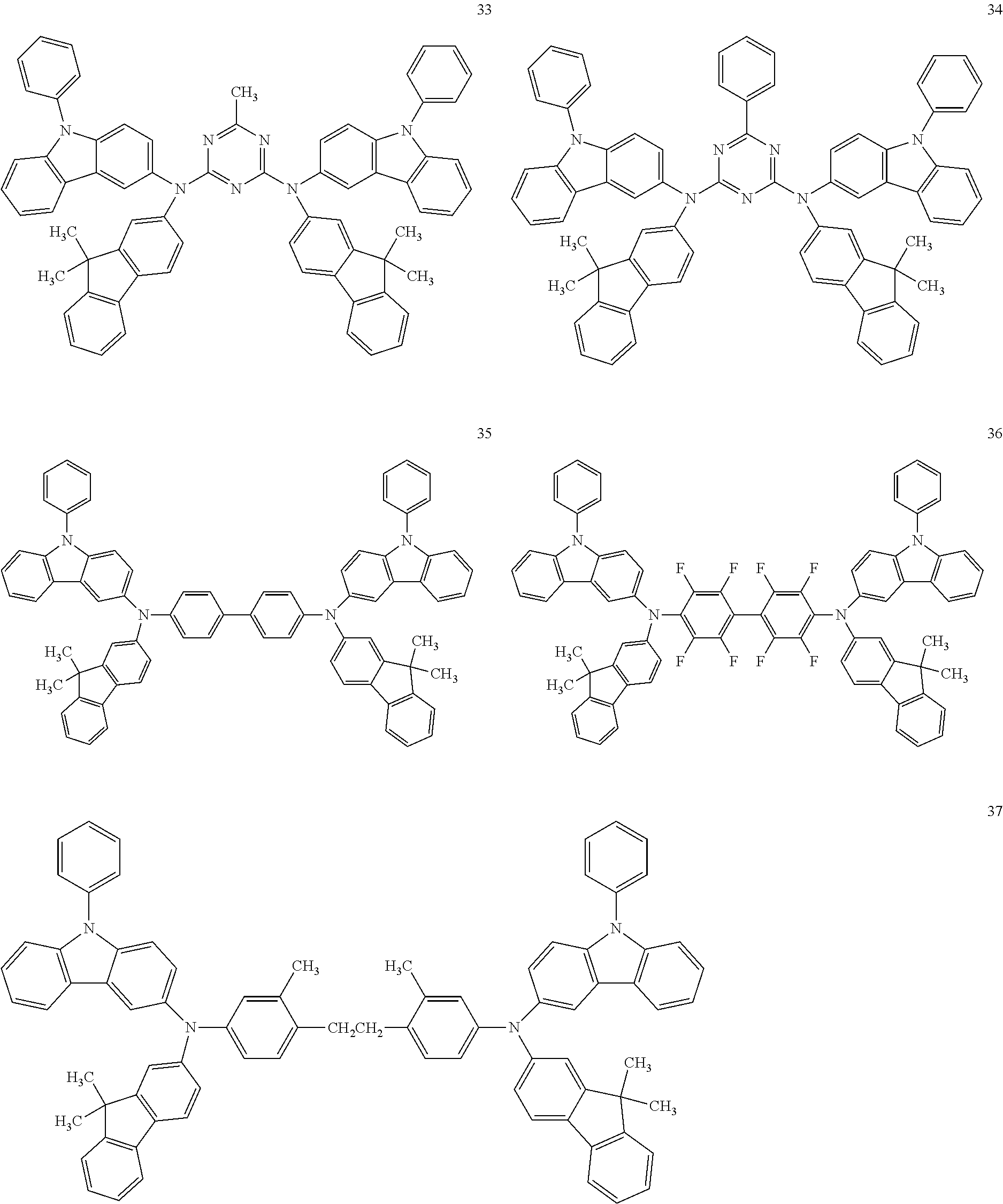
C00042

C00043

C00044

C00045
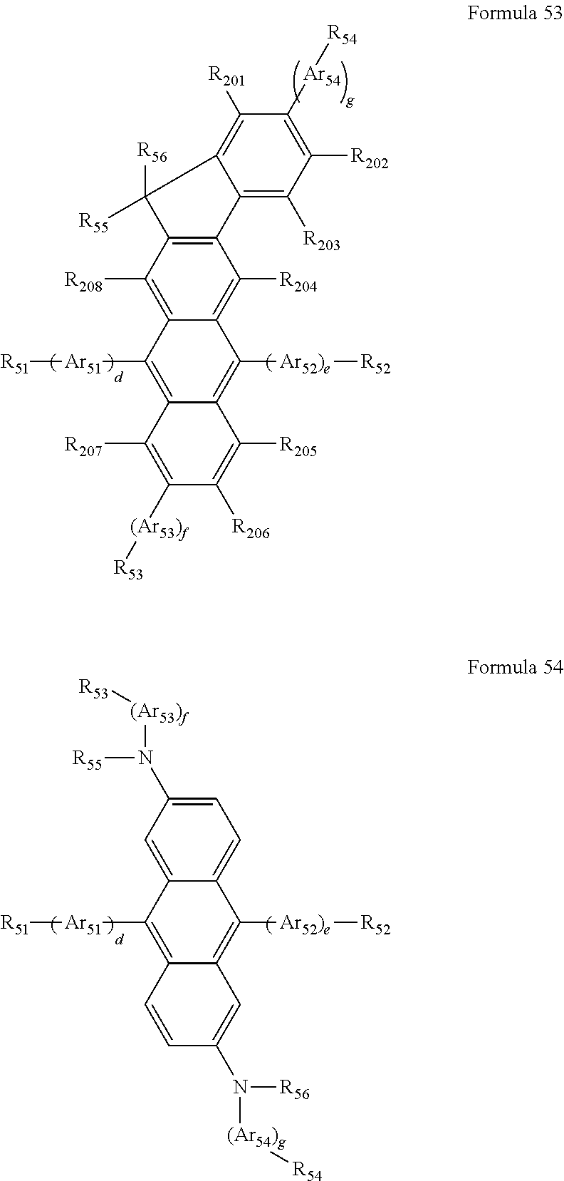
C00046

C00047

C00048

C00049

C00050
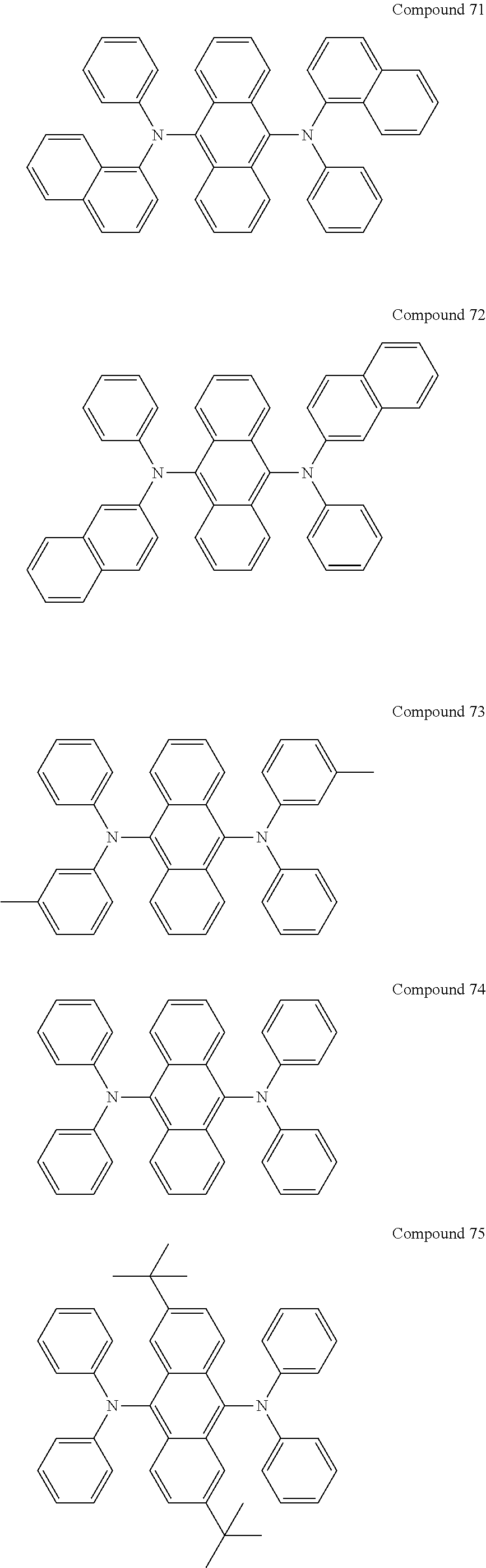
C00051
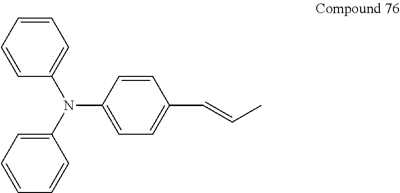
C00052

C00053

C00054
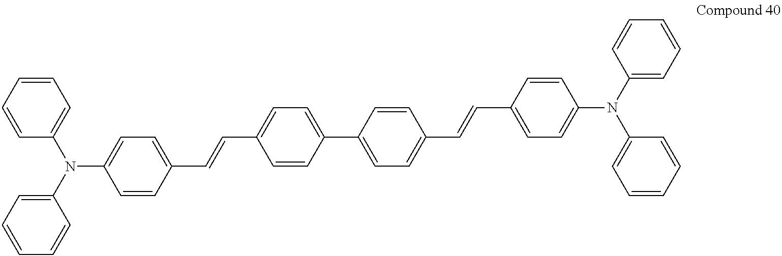
C00055

C00056
C00057

C00058
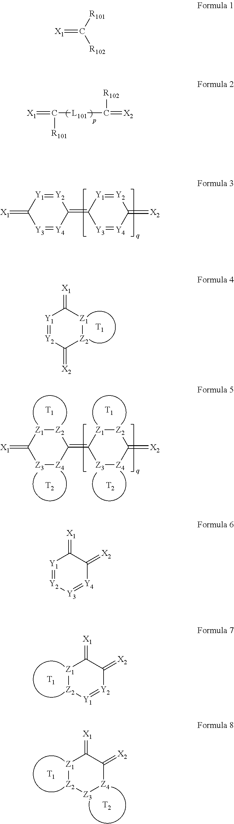
C00059

C00060
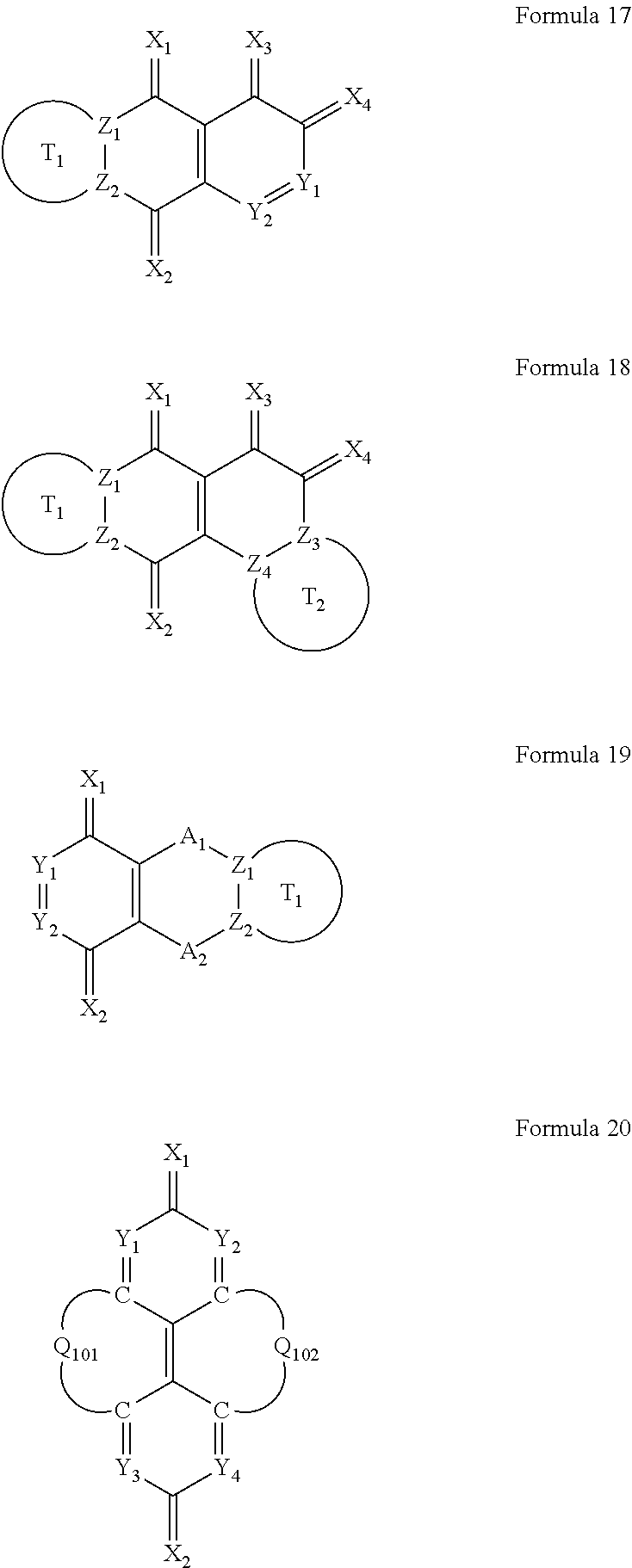
C00061

C00062

C00063

C00064
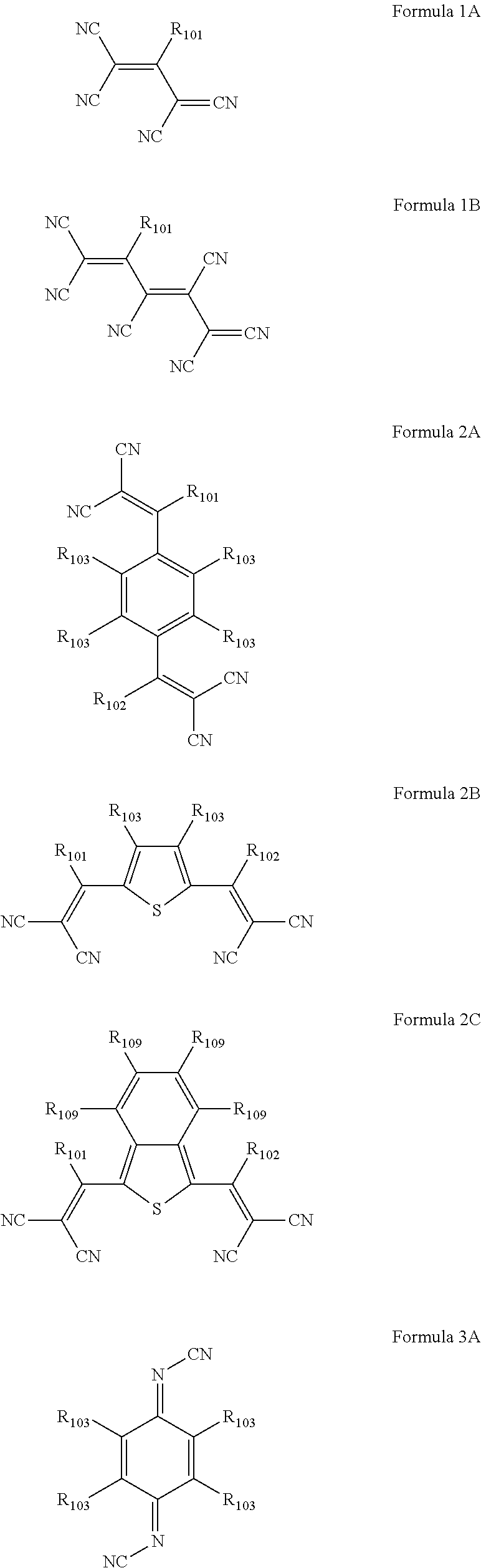
C00065

C00066

C00067
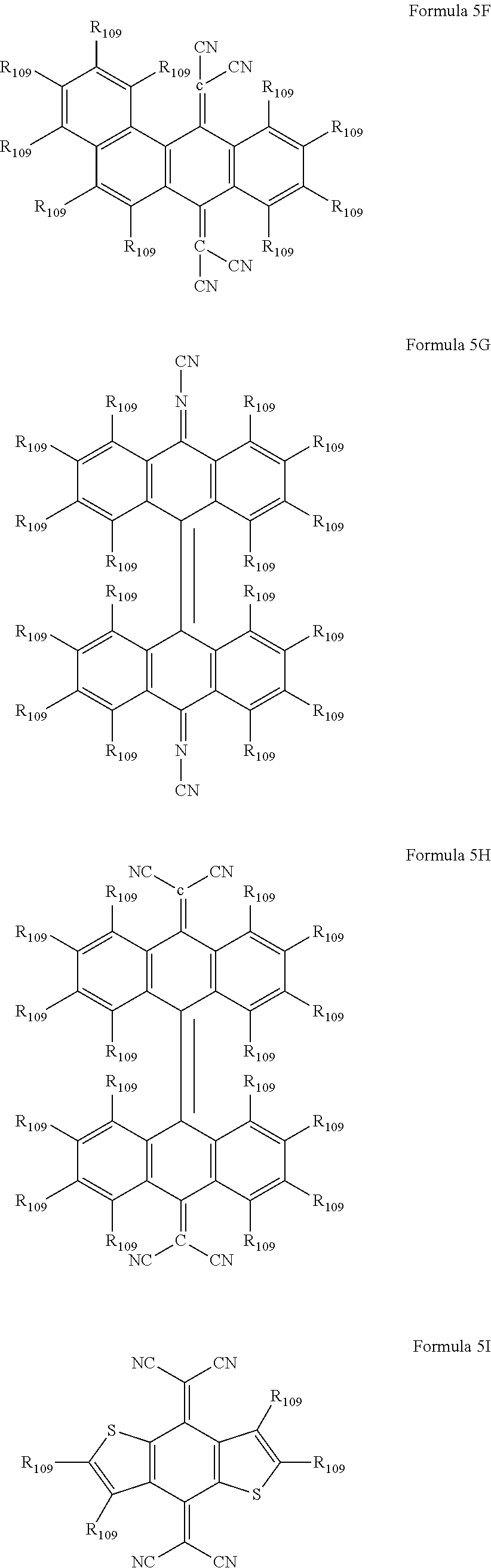
C00068

C00069

C00070

D00000

D00001
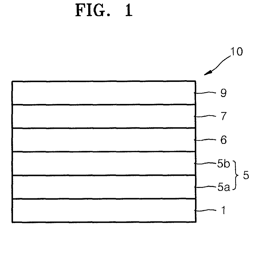
D00002
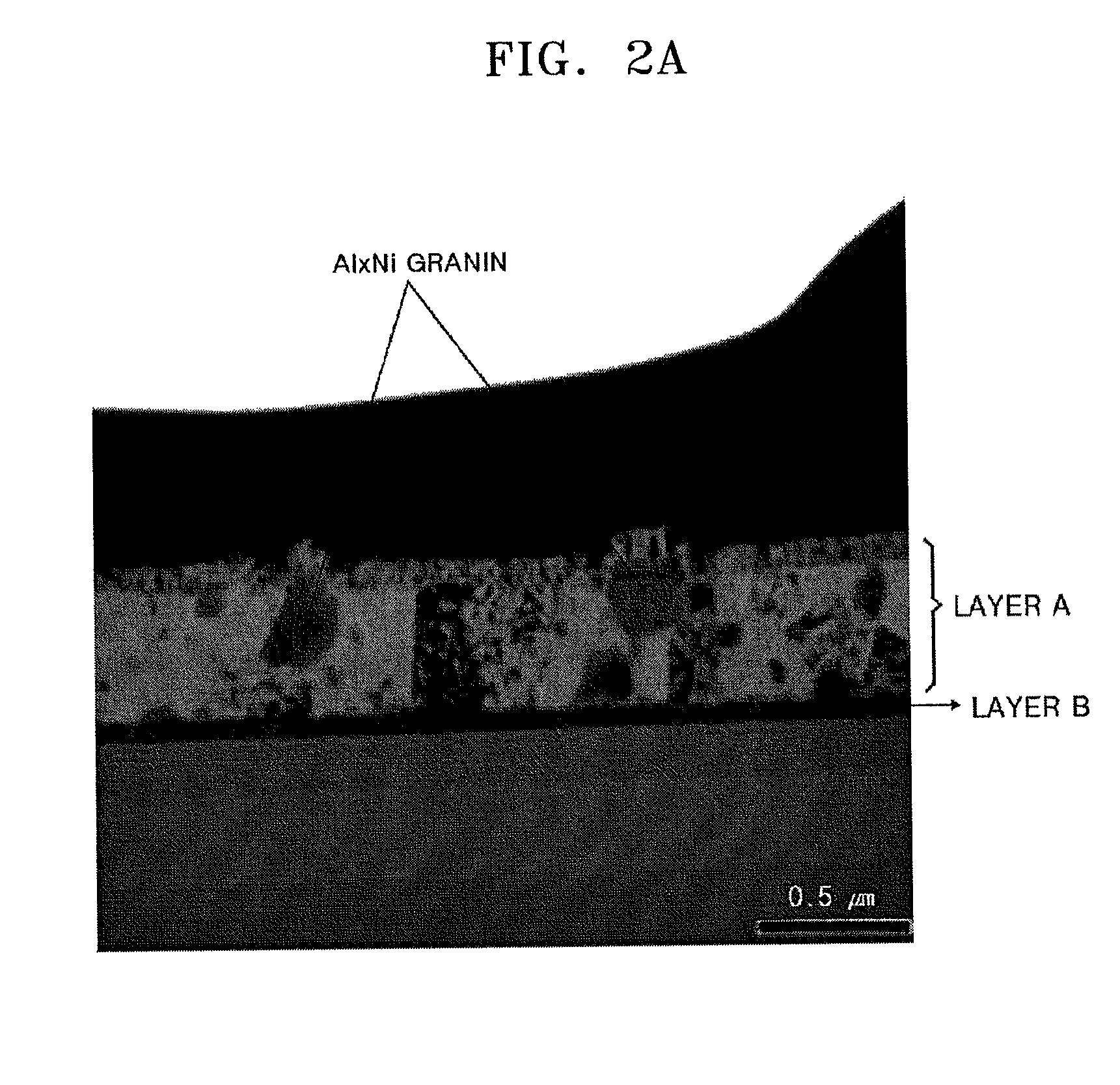
D00003
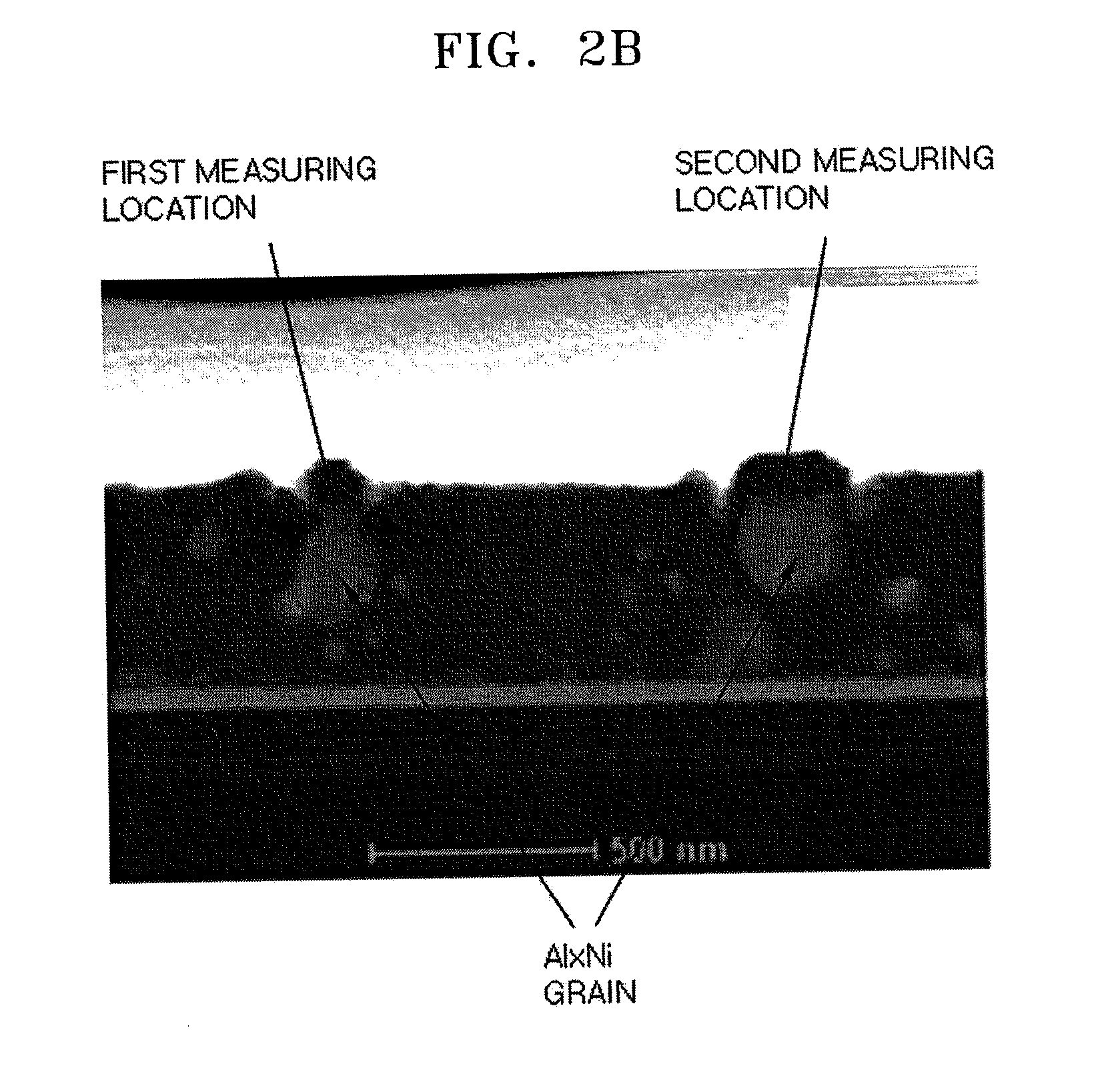
D00004

D00005
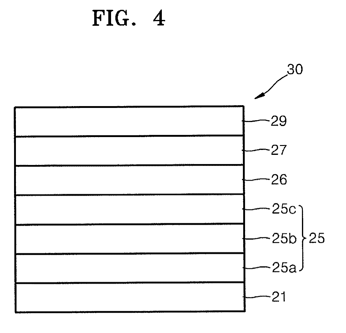
XML
uspto.report is an independent third-party trademark research tool that is not affiliated, endorsed, or sponsored by the United States Patent and Trademark Office (USPTO) or any other governmental organization. The information provided by uspto.report is based on publicly available data at the time of writing and is intended for informational purposes only.
While we strive to provide accurate and up-to-date information, we do not guarantee the accuracy, completeness, reliability, or suitability of the information displayed on this site. The use of this site is at your own risk. Any reliance you place on such information is therefore strictly at your own risk.
All official trademark data, including owner information, should be verified by visiting the official USPTO website at www.uspto.gov. This site is not intended to replace professional legal advice and should not be used as a substitute for consulting with a legal professional who is knowledgeable about trademark law.