Method for calibrating crystal frequency offset through radio frequency signal
Li , et al. April 5, 2
U.S. patent number 11,296,801 [Application Number 16/342,158] was granted by the patent office on 2022-04-05 for method for calibrating crystal frequency offset through radio frequency signal. This patent grant is currently assigned to Amlogic (Shanghai) Co., Ltd.. The grantee listed for this patent is Amlogic (Shanghai) Co., Ltd.. Invention is credited to Jie Feng, Shuangqing Li, Kun Zhang.

| United States Patent | 11,296,801 |
| Li , et al. | April 5, 2022 |
Method for calibrating crystal frequency offset through radio frequency signal
Abstract
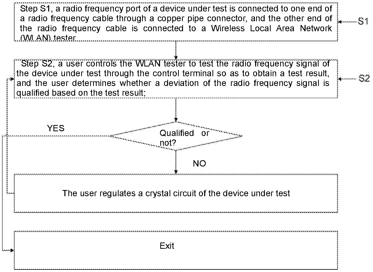
A method for calibrating crystal frequency offset through a radio frequency signal includes, in Step S1, a radio frequency port of a device is connected to one end of a radio frequency cable through a copper pipe connector and the other end of the radio frequency cable is connected to a Wireless Local Area Network (WLAN) tester which is connected with a control terminal. In Step S2, a user controls the WLAN tester to test the radio frequency signal of the device through the control terminal to obtain a test result, and determines whether a deviation of the radio frequency signal is qualified. If it is qualified, the user exits the test, otherwise the user regulates the crystal circuit of the device under test, and returns to Step S2. The method may not be affected by a probe, thus the measurement may be more accurate.
| Inventors: | Li; Shuangqing (Shanghai, CN), Zhang; Kun (Shanghai, CN), Feng; Jie (Shanghai, CN) | ||||||||||
|---|---|---|---|---|---|---|---|---|---|---|---|
| Applicant: |
|
||||||||||
| Assignee: | Amlogic (Shanghai) Co., Ltd.
(Shanghai, CN) |
||||||||||
| Family ID: | 63076865 | ||||||||||
| Appl. No.: | 16/342,158 | ||||||||||
| Filed: | October 31, 2018 | ||||||||||
| PCT Filed: | October 31, 2018 | ||||||||||
| PCT No.: | PCT/CN2018/113147 | ||||||||||
| 371(c)(1),(2),(4) Date: | April 15, 2019 | ||||||||||
| PCT Pub. No.: | WO2019/134429 | ||||||||||
| PCT Pub. Date: | July 11, 2019 |
Prior Publication Data
| Document Identifier | Publication Date | |
|---|---|---|
| US 20210336708 A1 | Oct 28, 2021 | |
Foreign Application Priority Data
| Jan 4, 2018 [CN] | 20181000852.7 | |||
| Current U.S. Class: | 1/1 |
| Current CPC Class: | G01R 29/0878 (20130101); H04B 17/21 (20150115); H04B 17/11 (20150115); H04W 84/12 (20130101) |
| Current International Class: | H04B 17/00 (20150101); H04B 17/11 (20150101); H04B 17/21 (20150101); G01R 29/08 (20060101); H04W 84/12 (20090101) |
References Cited [Referenced By]
U.S. Patent Documents
| 2008/0285467 | November 2008 | Olgaard |
| 2014/0146866 | May 2014 | Strachan |
| 2016/0202299 | July 2016 | Zaostrovnykh |
| 101150330 | Mar 2008 | CN | |||
| 101267230 | Sep 2008 | CN | |||
| 101399577 | Apr 2009 | CN | |||
| 103427916 | Dec 2013 | CN | |||
| 104683040 | Jun 2015 | CN | |||
Attorney, Agent or Firm: Levenfeld Pearlstein, LLC
Claims
What is claimed is:
1. A method for calibrating crystal frequency offset through a radio frequency signal which is applied to a crystal circuit, comprising: connecting, a step 1, a radio frequency port of a device under testing to one end of a radio frequency cable through a copper pipe connector, an opposite of the radio frequency cable being connected to a wireless local area network (WLAN) tester; controlling the WLAN tester to test a radio frequency signal of the device under testing through a control terminal to obtain a test result, a user determining whether a deviation of the radio frequency signal is qualified based on the test result; and controlling, at step 2, by a user, the WLAN tester to test the radio frequency signal of the device under testing through the control terminal to obtain a test result, the user determining whether a deviation of the radio frequency signal is qualified based on the test result; wherein if the test result shows that the deviation of the radio frequency signal is qualified, the user exits the test, and wherein if the test result shows that the deviation of the radio frequency signal is unqualified, the user regulates the crystal circuit of the device under testing, and returns to step 2.
2. The method for calibrating crystal frequency offset through a radio frequency signal of claim 1, wherein the WLAN tester comprises a test module and a control terminal module.
3. The method for calibrating crystal frequency offset through a radio frequency signal of claim 2, wherein the control terminal module is a PC port.
4. The method for calibrating crystal frequency offset through a radio frequency signal of claim 2, wherein the test module is connected to the control terminal module via a wired connection.
5. The method for calibrating crystal frequency offset through a radio frequency signal of claim 2, wherein in step 2, the user views the test result through a display device of the control terminal module.
6. The method for calibrating crystal frequency offset through a radio frequency signal of claim 1, wherein in step 2, when the user determines that a deviation of the radio frequency signal is unqualified based on the test result, the user regulates a capacitance value of a load capacitance of the crystal circuit.
7. The method for calibrating crystal frequency offset through a radio frequency signal of claim 1, wherein the radio frequency port of the device under test is an ANT.
Description
CROSS-REFERENCE TO RELATED APPLICATION DATA
This application is a US National Stage application of PCT/CN2018/113147, filed Oct. 31, 2018, which PCT application claims the benefit of and priority to Chinese Patent Application No. 201810008527.7, filed Jan. 4, 2018, the disclosures of which are incorporated herein in their entireties.
BACKGROUND OF THE INVENTION
1. Field of the Invention
The invention relates to the field of communication technologies, and more particularly, to a method for calibrating crystal frequency offset through a radio frequency signal.
2. Description of the Related Art
At present, as a frequency of a high-speed signal becomes increasingly higher, the requirement on the crystal frequency offset becomes more and more strict. When the load capacitance is incompatible with the crystal, an excessive large crystal frequency offset may occur and thus the system may become instable, and performance of Radio Frequency (RF) may be affected to a larger extent. A problem is stated as follows: due to the fact that the clock of the crystal and the external load capacitance are designed based on empirical values, it is difficult to meet the requirement on high precision clock. In addition, since the clock of the crystal and the non-essential resistance are designed based on empirical values, it is also difficult to meet the requirement on high precision clock.
Two technical solutions are put forward by those skilled in the art to solve the above-mentioned problem.
1. Directly measure the clock frequency on the transistor pin by using an oscilloscope, however, some problems can be found in the solution: the measurement is not accurate, the oscilloscope probe will affect the load capacitance, and thus, the offset is large.
2. Directly measure the clock frequency on the transistor pin by using a frequency meter, however, the load capacitance will be affected as well, leading to an inaccurate test result.
SUMMARY OF THE INVENTION
With respect to the foregoing problems in the prior art, the present invention provides a method for calibrating crystal frequency deviation through a radio frequency signal.
The technical solutions are as follows:
A method for calibrating crystal frequency offset through a radio frequency signal which is applied to a crystal circuit, comprising:
Step S1, a radio frequency port of a device under test being connected to one end of a radio frequency cable through a copper pipe connector, the other end of the radio frequency cable being connected to a Wireless Local Area Network (WLAN) tester; and
Step S2, a user controlling the Wireless Local Area Network tester to test the radio frequency signal of the device under test through the control terminal so as to obtain a test result, and the user determining whether a deviation of the radio frequency signal is qualified based on the test result;
if the result shows that the deviation of the radio frequency signal is qualified, the user exits the test;
and if the result shows that the deviation of the radio frequency signal is unqualified, the user regulates the crystal circuit of the device under test, and then turns to Step S2.
Preferably, the Wireless Local Area Network tester comprises a test module and a control terminal module.
Preferably, the control terminal module is a PC port.
Preferably, the test module is connected to the control terminal module via a wired connection.
Preferably, in Step S2, the user views the test result through a display device of the control terminal module.
Preferably, in Step S2, when the user determines that a deviation of the radio frequency signal is unqualified based on the test result, the user regulates a capacitance value of a load capacitance of the crystal circuit.
Preferably, the radio frequency port of the device under test is an ANT.
The technical solution set forth in the invention has the advantages that the method may not be affected by a probe, thus the measurement may be more accurate.
BRIEF DESCRIPTION OF THE DRAWINGS
The accompanying drawings, together with the specification, illustrate exemplary embodiments of the present disclosure, and, together with the description, serve to explain the principles of the present invention.
FIG. 1 is a flowchart of a method for calibrating crystal frequency offset through a radio frequency signal according to a preferred embodiment of the present invention;
FIG. 2 is a structure diagram of a method for calibrating crystal frequency offset through a radio frequency signal according to a preferred embodiment of the present invention.
DETAILED DESCRIPTION
The present invention will now be described more fully hereinafter with reference to the accompanying drawings, in which exemplary embodiments of the invention are shown. This invention may, however, be embodied in many different forms and should not be construed as limited to the embodiments set forth herein. Rather, these embodiments are provided so that this disclosure will be thorough and complete, and will fully convey the scope of the invention to those skilled in the art. Like reference numerals refer to like elements throughout.
The terminology used herein is for the purpose of describing particular embodiments only and is not intended to be limiting of the invention. As used herein, the singular forms "a", "an" and "the" are intended to include the plural forms as well, unless the context clearly indicates otherwise. It will be further understood that the terms "comprises" and/or "comprising," or "includes" and/or "including" or "has" and/or "having" when used herein, specify the presence of stated features, regions, integers, steps, operations, elements, and/or components, but do not preclude the presence or addition of one or more other features, regions, integers, steps, operations, elements, components, and/or groups thereof.
Unless otherwise defined, all terms (including technical and scientific terms) used herein have the same meaning as commonly understood by one of ordinary skill in the art to which this invention belongs. It will be further understood that terms, such as those defined in commonly used dictionaries, should be interpreted as having a meaning that is consistent with their meaning in the context of the relevant art and the present disclosure, and will not be interpreted in an idealized or overly formal sense unless expressly so defined herein.
As used herein, the term "plurality" means a number greater than one.
Hereinafter, certain exemplary embodiments according to the present disclosure will be described with reference to the accompanying drawings.
As shown in FIGS. 1 and 2, a method for calibrating crystal frequency offset through a radio frequency signal comprises:
Step S1, a radio frequency port of a device under test 1 is connected to one end of a radio frequency cable 3 through a copper pipe connector 2, the other end of the radio frequency cable 3 is connected to a test module 4 of a Wireless Local Area Network tester, IQFlex (the Wireless Local Area Network tester comprises the test module 4 and a control terminal module 5, when the control terminal module 5 is omitted, the test module 4 may be the IQFlex itself which is commonly used by those skilled in the art), and the test module 4 is connected to the control terminal module; and
Step S2, a user controls the test module 4 to test the radio frequency signal of the device under test 1 through the control terminal module 5 so as to obtain a test result, and the user determines whether a deviation of the radio frequency signal is qualified based on the test result;
if the result shows that the deviation of the radio frequency signal is qualified, the user exits the test;
and if the result shows that the deviation of the radio frequency signal is unqualified, the user regulates the crystal circuit of the device under test 1, and then turns to Step S2.
In a preferred embodiment, the radio frequency port of the device under test 1 is an ANT.
In a preferred embodiment, the test module 4 is connected to the control terminal module 5 via a wired connection.
In a preferred embodiment, the control terminal module 5 is a PC port.
In a preferred embodiment, in Step S2, the user views the test result through a display device of the control terminal module 5.
In a preferred embodiment, when the user determines that a deviation of the radio frequency signal is unqualified based on the test result, the user regulates a capacitance value of a load capacitance of the crystal circuit.
In this embodiment, the RF is tested by using IQFlex so as to regulate a matching capacitance of the crystal, and to calibrate a clock of WIFI.
The test method is described in detail as follows: firstly, a radio frequency (RF) port of a device under test (DUT) is connected to a radio frequency (RF) cable through the copper pipe connector 2; the device under test is connected to the test device IQFlex though the RF cable; then IQFlex is connected to the PC for conducting the test. By conducting a RF index test, the deviation of the frequency offset of a crystal oscillator clock may be displayed on a PC interface. In this case, the load capacitance is regulated, the frequency offset is regulated to a smaller value, and clock offset is reduced accordingly. The method would not be affected by a probe, thus the measurement is more accurate.
The above descriptions are only the preferred embodiments of the invention, not thus limiting the embodiments and scope of the invention. Those skilled in the art should be able to realize that the schemes obtained from the content of specification and drawings of the invention are within the scope of the invention.
* * * * *
D00000
D00001
XML
uspto.report is an independent third-party trademark research tool that is not affiliated, endorsed, or sponsored by the United States Patent and Trademark Office (USPTO) or any other governmental organization. The information provided by uspto.report is based on publicly available data at the time of writing and is intended for informational purposes only.
While we strive to provide accurate and up-to-date information, we do not guarantee the accuracy, completeness, reliability, or suitability of the information displayed on this site. The use of this site is at your own risk. Any reliance you place on such information is therefore strictly at your own risk.
All official trademark data, including owner information, should be verified by visiting the official USPTO website at www.uspto.gov. This site is not intended to replace professional legal advice and should not be used as a substitute for consulting with a legal professional who is knowledgeable about trademark law.