Lighting apparatus
Chen , et al. June 1, 2
U.S. patent number 11,021,653 [Application Number 16/570,666] was granted by the patent office on 2021-06-01 for lighting apparatus. This patent grant is currently assigned to LEEDARSON LIGHTING CO. LTD.. The grantee listed for this patent is LEEDARSON LIGHTING CO. LTD.. Invention is credited to Liangliang Cao, Huiwu Chen, Yanbiao Chen, Qiyuan Wang.


| United States Patent | 11,021,653 |
| Chen , et al. | June 1, 2021 |
Lighting apparatus
Abstract
A LED device includes LED chips mounted on a substrate, a first fluorescent layer, a second fluorescent layer and a package housing. The LED chips emit a blue light. The first fluorescent layer has a first side facing to the LED chips for converting the blue light to a red light. The second fluorescent layer has a first side attached to a second side of the first fluorescent layer for converting the blue light to a red light emitted from a second side of the second fluorescent layer. The package housing holds the substrate and the first fluorescent layer.
| Inventors: | Chen; Yanbiao (Xiamen, CN), Cao; Liangliang (Xiamen, CN), Chen; Huiwu (Xiamen, CN), Wang; Qiyuan (Xiamen, CN) | ||||||||||
|---|---|---|---|---|---|---|---|---|---|---|---|
| Applicant: |
|
||||||||||
| Assignee: | LEEDARSON LIGHTING CO. LTD.
(Fujian, CN) |
||||||||||
| Family ID: | 1000005588626 | ||||||||||
| Appl. No.: | 16/570,666 | ||||||||||
| Filed: | September 13, 2019 |
Prior Publication Data
| Document Identifier | Publication Date | |
|---|---|---|
| US 20200002606 A1 | Jan 2, 2020 | |
Related U.S. Patent Documents
| Application Number | Filing Date | Patent Number | Issue Date | ||
|---|---|---|---|---|---|
| 16279154 | Feb 19, 2019 | 10450504 | |||
| 15886801 | Apr 2, 2019 | 10246636 | |||
Foreign Application Priority Data
| Jan 16, 2018 [CN] | 201820071681.4 | |||
| Current U.S. Class: | 1/1 |
| Current CPC Class: | H01L 33/52 (20130101); C09K 11/59 (20130101); F21K 9/64 (20160801); C08K 3/34 (20130101); H01L 33/504 (20130101); H01L 33/50 (20130101); H01L 33/486 (20130101); C09K 11/0883 (20130101); H01L 2933/0041 (20130101); H01L 25/0753 (20130101); H01L 33/505 (20130101) |
| Current International Class: | C09K 11/08 (20060101); C09K 11/59 (20060101); H01L 33/52 (20100101); H01L 33/48 (20100101); H01L 33/50 (20100101); F21K 9/64 (20160101); C08K 3/34 (20060101); H01L 25/075 (20060101) |
References Cited [Referenced By]
U.S. Patent Documents
| 10450504 | October 2019 | Chen |
| 2018/0322824 | November 2018 | Martin |
Assistant Examiner: Diaz; Jose M
Attorney, Agent or Firm: Shih; Chun-Ming Lanway IPR Services
Parent Case Text
RELATED APPLICATION
The present application is a continued application of U.S. patent application Ser. No. 16/279,154.
Claims
The invention claimed is:
1. A lighting apparatus, comprising: a LED device comprising a LED module comprising multiple LED chips mounted on a first terminal area and a second terminal area, the first terminal area being mounted with more LED chips than and the second terminal area, a first fluorescent layer with a first side facing to the LED module, and a package housing for holding a substrate and the first fluorescent layer; and a driver for supplying a driving current to the first terminal area and the second terminal area.
2. The lighting apparatus of claim 1, wherein the multiple LED chips emit a blue light, the first terminal area and the second terminal area are provided for respectively connected to a positive terminal and a negative terminal of a power source, there are wires electrically connected the LED chips on the first terminal area and the second terminal area.
3. The lighting apparatus of claim 1, wherein the first fluorescent layer comprises red phosphor material contained in first silicone part, a second fluorescent layer upon the first fluorescent layer comprises green phosphor material contained in a second silicone part, and wherein a part of the green light excites the red phosphor if the green light hits the red phosphor.
4. The lighting apparatus of claim 3, wherein a first volume ratio of the red phosphor to the first silicone part is larger than a second volume ratio of the green phosphor to the second silicone part.
5. The lighting apparatus of claim 3, wherein a first volume ratio of the red phosphor to the first silicone part is smaller than a second volume ratio of the green phosphor to the second silicone part.
6. The lighting apparatus of claim 1, wherein a thickness of the first fluorescent layer is larger than a thickness of the second fluorescent layer.
7. The lighting apparatus of claim 1, wherein a thickness of the first fluorescent layer is smaller than a thickness of the second fluorescent layer.
8. The lighting apparatus of claim 1, wherein the first fluorescent layer has better heat resisting feature than the second fluorescent layer.
9. The lighting apparatus of claim 1, wherein the package housing has a bottom part fixed to the substrate and the package housing has a surrounding wall extended from the bottom part, the wall defines a containing space for holding the first fluorescent layer.
10. The lighting apparatus of claim 9, wherein a second side of the second fluorescent layer has a curved surface.
11. The lighting apparatus of claim 10, wherein an angle of edges of the first side and the second side of the second fluorescent layer is less than 60 degrees.
12. The lighting apparatus of claim 10, wherein the curve surface forms a convex lens.
13. The lighting apparatus of claim 1, wherein area of the second side of the second fluorescent layer is smaller than area of the second side of the first fluorescent layer.
14. The lighting apparatus of claim 13, wherein a part of the second side of the first fluorescent layer is exposed and uncovered by the second fluorescent layer.
15. The lighting apparatus of claim 14, wherein the second side of second fluorescent layer is surrounded by the second side of the first fluorescent layer from a top view.
16. The lighting apparatus of claim 1, wherein the package housing has a ladder wall for engaging with a peripheral part of the second fluorescent layer.
17. The lighting apparatus of claim 16, wherein the second side of the second fluorescent layer forms a flat surface.
18. The lighting apparatus of claim 16, wherein the second side of second florescent layer forms a curve surface.
19. The lighting apparatus of claim 1, wherein the second side of the second fluorescent layer has multiple convex part corresponding to multiple underlying LED chips of the LED module.
20. The lighting apparatus of claim 1, wherein the LED module is mounted on the substrate with surface mount device (SMD) technology.
Description
FIELD OF THE INVENTION
The present invention is related to a lighting apparatus and more particularly related to a lighting apparatus with LED devices.
BACKGROUND
After years of hard working, LED products have been widely spread over the world. At beginning, the cost of LED products is too high, preventing LED products to be popular. Nowadays, LED product price has lowered to an acceptable level.
However, it is always important to further find every aspect to improve such devices, particularly for such worldwide products related to human daily life. Heat efficiency, color rendering index, and more characteristics need to consider when designing LED devices.
In the present invention, inventors look deeper into the LED basic structure and finds several inventive points to further improve LED device performance.
SUMMARY OF INVENTION
According to a first embodiment of the present invention, a LED (light emitted diode) device is provided. The LED device has a LED module, a first fluorescent layer, a second fluorescent layer, and a package housing.
The LED module is mounted on a substrate for emitting a blue light.
The first fluorescent layer has a first side facing to the LED module for converting the blue light to a red light.
The second fluorescent layer has a first side attached to a second side of the first fluorescent layer for converting the blue light to a red light emitted from a second side of the second fluorescent layer.
The package housing holds the substrate and the first fluorescent layer.
With such design, the first fluorescent layer is between the second fluorescent layer and the LED module. In other words, a blue light emitted from the LED module firstly enters the first fluorescent layer, hitting certain phosphor material and generating corresponding red light. In addition, some part of the blue light further moves to the second fluorescent layer to hit other phosphor material to generate green light. With red light and green light, users may see a white light effect.
In some embodiments, the LED module has multiple LED chips emitting the blue light. The substrate has a first terminal area and a second terminal area for mounting the multiple LED chips. For example, multiple LED chips are mounted on conductive plates used as the terminal areas with surface mounting device (SMD) technology.
The first terminal area and the second terminal area are provided for respectively connected to a positive terminal and a negative terminal of a power source. The first terminal area may have different size as the second terminal area. For example, when there are more LED chips mounted on the first terminal area than on the second terminal area, the first terminal area may have a larger size than the second terminal area to provide better heat dissipation effect.
In some embodiments, the first fluorescent has red phosphor material contained in first silicone part, and the second fluorescent layer has green phosphor material contained in a second silicone part. Please be noted that other materials in addition to silica gel, like resin, may be used for containing phosphor powder.
In addition, a part of the green light may excite the red phosphor if the green light hits the red phosphor. In other words, if the blue light firstly enters the second fluorescent layer, the blue light may firstly be converted to green light. If such green light continues to move into the first fluorescent layer, part or all of the green light may be consumed and converted into red light. This may decrease the overall green light energy and decreases an overall CRI (color rendering index) of the LED device.
Therefore, it is beneficial to place the first fluorescent layer between the second fluorescent layer and the LED module, for improving green light output and deceasing undesired consumption of the green light output.
Inventors also find that there the volume ratio of phosphor material in the first fluorescent layer and the second fluorescent layer may be adjusted to further improve different characteristics of the LED device.
In some cases, a first volume ratio of the red phosphor to the first silicone part is larger than a second volume ratio of the green phosphor to the second silicone part.
In some other cases, a first volume ratio of the red phosphor to the first silicone part is smaller than a second volume ratio of the green phosphor to the second silicone part.
The provide different features and characteristics, suitable for making various LED products.
In some embodiments, a thickness of the first fluorescent layer is larger than a thickness of the second fluorescent layer.
In some other embodiments, a thickness of the first fluorescent layer is smaller than a thickness of the second fluorescent layer.
Such variations are found helpful for adjusting product characteristic of the LED device.
In addition, the first fluorescent layer may have better heat resisting feature than the second fluorescent layer, when the first fluorescent layer is placed closer to the LED module.
In other words, designers may place phosphor material with less heat resisting characteristic as the second fluorescent layer.
In some embodiments, the package housing may have a bottom part fixed to the substrate and the package housing has a surrounding wall extended from the bottom part. The wall defines a containing space for holding the first fluorescent layer.
For example, the package housing has a hole for holding the substrate and four connecting walls forming a rectangular containing space. The first fluorescent layer and sometimes the second florescent layer are placed in the containing space.
There are several ways to design the second fluorescent layer.
In some embodiments, a second side of the second fluorescent layer has a curved surface. In other words, the top surface of the second fluorescent layer may have a curve surface.
Specifically, an angle of edges of the first side and the second side of the second fluorescent layer would be less than 60 degrees. Such design may increase overall product stability.
In some embodiments, the curve surface forms a convex lens, providing better optical characteristic for output light, by directing light to desired direction.
In some other embodiments, area of the second side of the second fluorescent layer is smaller than area of the second side of the first fluorescent layer. In other words, when being looked over a top view, a part of the second side of the first fluorescent layer is exposed and uncovered by the second fluorescent layer.
In such case, there is an embodiment to place the second fluorescent in the middle place, which causes the second side of second fluorescent layer being surrounded by the second side of the first fluorescent layer from a top view.
In some embodiments, the package housing has a ladder wall for engaging with a peripheral part of the second fluorescent layer. In some manufacturing procedures, the first fluorescent layer and the second fluorescent layer are heated as gel mode to be filled into the package holding. When the package holding has a ladder wall, the first fluorescent layer may be filled in a first ladder while the second fluorescent layer may be filled to in a second ladder upper than the first ladder in the ladder wall.
In some embodiments, the second side of the second fluorescent layer forms a flat surface.
In some other embodiments, the second side of second florescent layer forms a curve surface for different optical characteristic requirement.
In some embodiments, the second side of the second fluorescent layer may have multiple convex part corresponding to multiple underlying LED chips of the LED module. It may be implemented by applying gel mode material of the second fluorescent layer to the package for several times respectively to underlying LED chips. Because LED chips usually have certain light emitting angle, it is helpful to maximize the light converting effect by placing more material of the second fluorescent layer on top of corresponding LED chips, particularly when phosphor material is critical cost in LED devices.
BRIEF DESCRIPTION OF DRAWINGS
FIG. 1 is a diagram illustrating a LED device embodiment.
FIG. 2 is a top view of FIG. 1.
FIG. 3. Illustrates a first fluorescent layer installed in a LED device embodiment.
FIG. 4 illustrates a top view of FIG. 3.
FIG. 5 illustrates a first way to add a second fluorescent layer.
FIG. 6 illustrates a top view of FIG. 5.
FIG. 7 illustrates another way to add a second fluorescent layer.
FIG. 8 illustrates a top view of FIG. 7.
FIG. 9 illustrates another way to add a second fluorescent layer.
FIG. 10 illustrates LED chips in an embodiment.
FIG. 11 illustrates another side view of a LED device embodiment.
FIG. 12 illustrates a top view of a LED device embodiment.
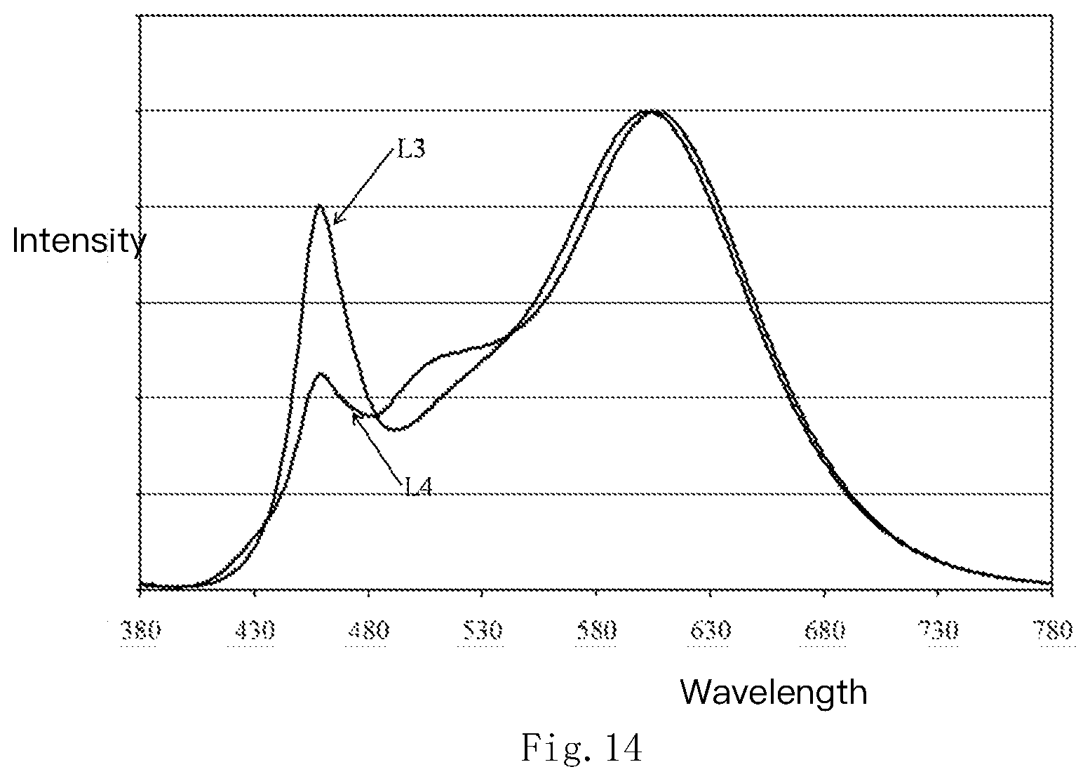
FIG. 13 illustrates a optical characteristic diagram of an experimental result.
FIG. 14 illustrates another optical characteristic diagram of an experimental result.
DETAILED DESCRIPTION
According to a first embodiment of the present invention, a LED (light emitted diode) device is provided. The LED device has a LED module, a first fluorescent layer, a second fluorescent layer, and a package housing.
The LED module is mounted on a substrate for emitting a blue light.
The first fluorescent layer has a first side facing to the LED module for converting the blue light to a red light.
The second fluorescent layer has a first side attached to a second side of the first fluorescent layer for converting the blue light to a red light emitted from a second side of the second fluorescent layer.
The package housing holds the substrate and the first fluorescent layer.
With such design, the first fluorescent layer is between the second fluorescent layer and the LED module. In other words, a blue light emitted from the LED module firstly enters the first fluorescent layer, hitting certain phosphor material and generating corresponding red light. In addition, some part of the blue light further moves to the second fluorescent layer to hit other phosphor material to generate green light. With red light and green light, users may see a white light effect.
In some embodiments, the LED module has multiple LED chips emitting the blue light. The substrate has a first terminal area and a second terminal area for mounting the multiple LED chips. For example, multiple LED chips are mounted on conductive plates used as the terminal areas with surface mounting device (SMD) technology.
The first terminal area and the second terminal area are provided for respectively connected to a positive terminal and a negative terminal of a power source. The first terminal area may have different size as the second terminal area. For example, when there are more LED chips mounted on the first terminal area than on the second terminal area, the first terminal area may have a larger size than the second terminal area to provide better heat dissipation effect.
In some embodiments, the first fluorescent has red phosphor material contained in first silicone part, and the second fluorescent layer has green phosphor material contained in a second silicone part. Please be noted that other materials in addition to silica gel, like resin, may be used for containing phosphor powder.
In addition, a part of the green light may excite the red phosphor if the green light hits the red phosphor. In other words, if the blue light firstly enters the second fluorescent layer, the blue light may firstly be converted to green light. If such green light continues to move into the first fluorescent layer, part or all of the green light may be consumed and converted into red light. This may decrease the overall green light energy and decreases an overall CRI (color rendering index) of the LED device.
Therefore, it is beneficial to place the first fluorescent layer between the second fluorescent layer and the LED module, for improving green light output and deceasing undesired consumption of the green light output.
Inventors also find that there the volume ratio of phosphor material in the first fluorescent layer and the second fluorescent layer may be adjusted to further improve different characteristics of the LED device.
In some cases, a first volume ratio of the red phosphor to the first silicone part is larger than a second volume ratio of the green phosphor to the second silicone part.
In some other cases, a first volume ratio of the red phosphor to the first silicone part is smaller than a second volume ratio of the green phosphor to the second silicone part.
The provide different features and characteristics, suitable for making various LED products.
In some embodiments, a thickness of the first fluorescent layer is larger than a thickness of the second fluorescent layer.
In some other embodiments, a thickness of the first fluorescent layer is smaller than a thickness of the second fluorescent layer.
Such variations are found helpful for adjusting product characteristic of the LED device.
In addition, the first fluorescent layer may have better heat resisting feature than the second fluorescent layer, when the first fluorescent layer is placed closer to the LED module. In other words, designers may place phosphor material with less heat resisting characteristic as the second fluorescent layer.
In some embodiments, the package housing may have a bottom part fixed to the substrate and the package housing has a surrounding wall extended from the bottom part. The wall defines a containing space for holding the first fluorescent layer.
For example, the package housing has a hole for holding the substrate and four connecting walls forming a rectangular containing space. The first fluorescent layer and sometimes the second florescent layer are placed in the containing space.
There are several ways to design the second fluorescent layer.
In some embodiments, a second side of the second fluorescent layer has a curved surface. In other words, the top surface of the second fluorescent layer may have a curve surface.
Specifically, an angle of edges of the first side and the second side of the second fluorescent layer would be less than 60 degrees. Such design may increase overall product stability.
In some embodiments, the curve surface forms a convex lens, providing better optical characteristic for output light, by directing light to desired direction.
In some other embodiments, area of the second side of the second fluorescent layer is smaller than area of the second side of the first fluorescent layer. In other words, when being looked over a top view, a part of the second side of the first fluorescent layer is exposed and uncovered by the second fluorescent layer.
In such case, there is an embodiment to place the second fluorescent in the middle place, which causes the second side of second fluorescent layer being surrounded by the second side of the first fluorescent layer from a top view.
In some embodiments, the package housing has a ladder wall for engaging with a peripheral part of the second fluorescent layer. In some manufacturing procedures, the first fluorescent layer and the second fluorescent layer are heated as gel mode to be filled into the package holding. When the package holding has a ladder wall, the first fluorescent layer may be filled in a first ladder while the second fluorescent layer may be filled to in a second ladder upper than the first ladder in the ladder wall.
In some embodiments, the second side of the second fluorescent layer forms a flat surface.
In some other embodiments, the second side of second florescent layer forms a curve surface for different optical characteristic requirement.
In some embodiments, the second side of the second fluorescent layer may have multiple convex part corresponding to multiple underlying LED chips of the LED module. It may be implemented by applying gel mode material of the second fluorescent layer to the package for several times respectively to underlying LED chips. Because LED chips usually have certain light emitting angle, it is helpful to maximize the light converting effect by placing more material of the second fluorescent layer on top of corresponding LED chips, particularly when phosphor material is critical cost in LED devices.
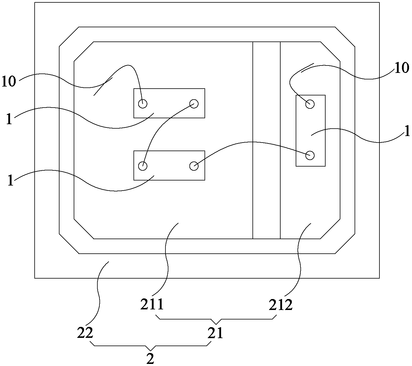
Please refer to FIG. 1 to FIG. 6, illustrating a LED device embodiment.
The LED device has LED chips 1 and a bracket 2 for fixing the LED chips 1. The LED bracket 2 contains a substrate 21 and four side walls 22 as a package housing. The substrate 21 and the side walls 22 form a containing space 23.
A first terminal area 211 and a second terminal area 212 are disposed on the substrate. The LED chips 1 are placed in the containing space 23 and mounted on surface of the first terminal area 211 and the second terminal area 212, e.g. via surface mounting device (SMD) technology. The LED chips 1 may be electrically connected in series or in other combination. The first terminal area 211 and the second terminal 212 are further electrically connected to a power source to supply electricity to the LED chips 1.
A first fluorescent layer 31 is disposed for covering the LED chips 1. A second fluorescent layer 32 is on top of the first fluorescent layer 31. The wave length of emitted light of the first fluorescent layer 31 is longer than the wave length of emitted light of the second fluorescent layer 32 when a blue light or an ultraviolet light is respectively emitted into the first fluorescent layer 31 and the second fluorescent layer 32. For example, the first fluorescent layer emits red light when blue light enters the first fluorescent layer 31, and the second fluorescent layer emits green light when blue light enters the second fluorescent layer 32.
In addition, the first fluorescent layer 31 may be made by mixing red phosphor in a silicone material, and the second fluorescent layer 32 may be made by mixing green phosphor in a silicone material.
The LED chips 1 may be LED chips emitting blue light of wavelengths within range 380 nm to 460 nm. The green light emitted from the second fluorescent layer 31 may be within range 500 nm to 560 nm. The red light emitted from the first fluorescent layer 32 may be within 600 nm to 670 nm.
Some blue light is not absorbed by either the first fluorescent layer 31 or the second fluorescent layer 32. Therefore, in some embodiment, the overall output light includes blue light, red light and green light, which together form a white light.
With such design, green light is not consumed by red phosphor material and further improves CRI (color rendering index) and overall luminous efficacy.
Please be noted that the embodiment is only for explaining the inventive concept, instead of limiting the inventive scope. Other variations may be made by persons of ordinary skilled in the art based on disclosure of this specification.
The bracket 2 may be SMD bracket made of PCT material, a mixture of CHDM (1,4-Cyclohexanedimethanol) and DMT (Terephthalic acid dimethyl ester).
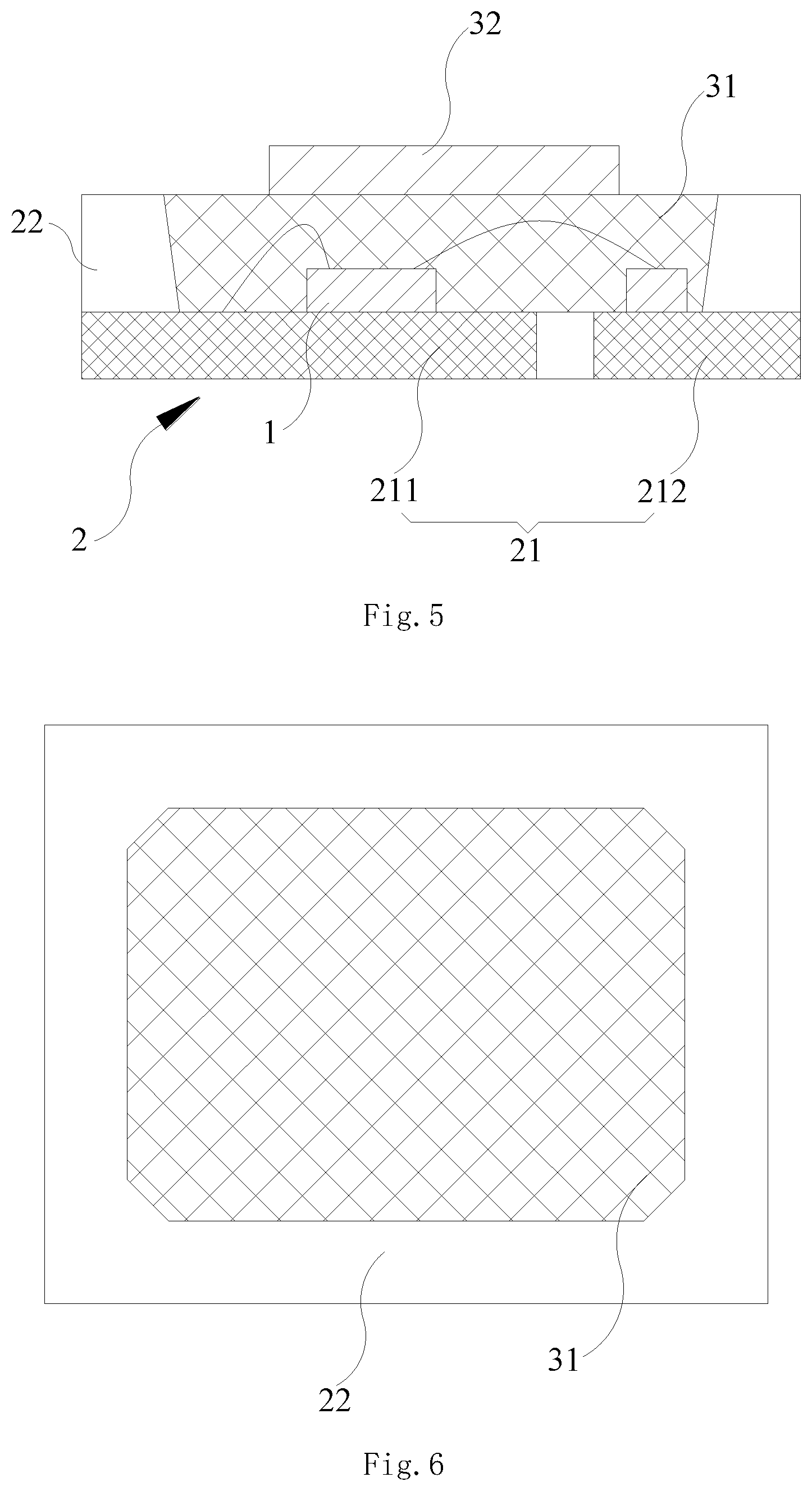
Please refer to FIG. 5 and FIG. 6. In one embodiment, the first fluorescent layer 31 is disposed in the containing space 23. The top surface of the second side of the first fluorescent layer 31 is aligned with the top surface of the side walls 22.
The first side of the second fluorescent layer 32 is placed on top of the first fluorescent layer 31. The size of the second side of the second fluorescent layer 32 is smaller than the size of the second side of the first fluorescent layer 31. Therefore, part of the first fluorescent layer 31 is exposed and uncovered by the second fluorescent layer 32.
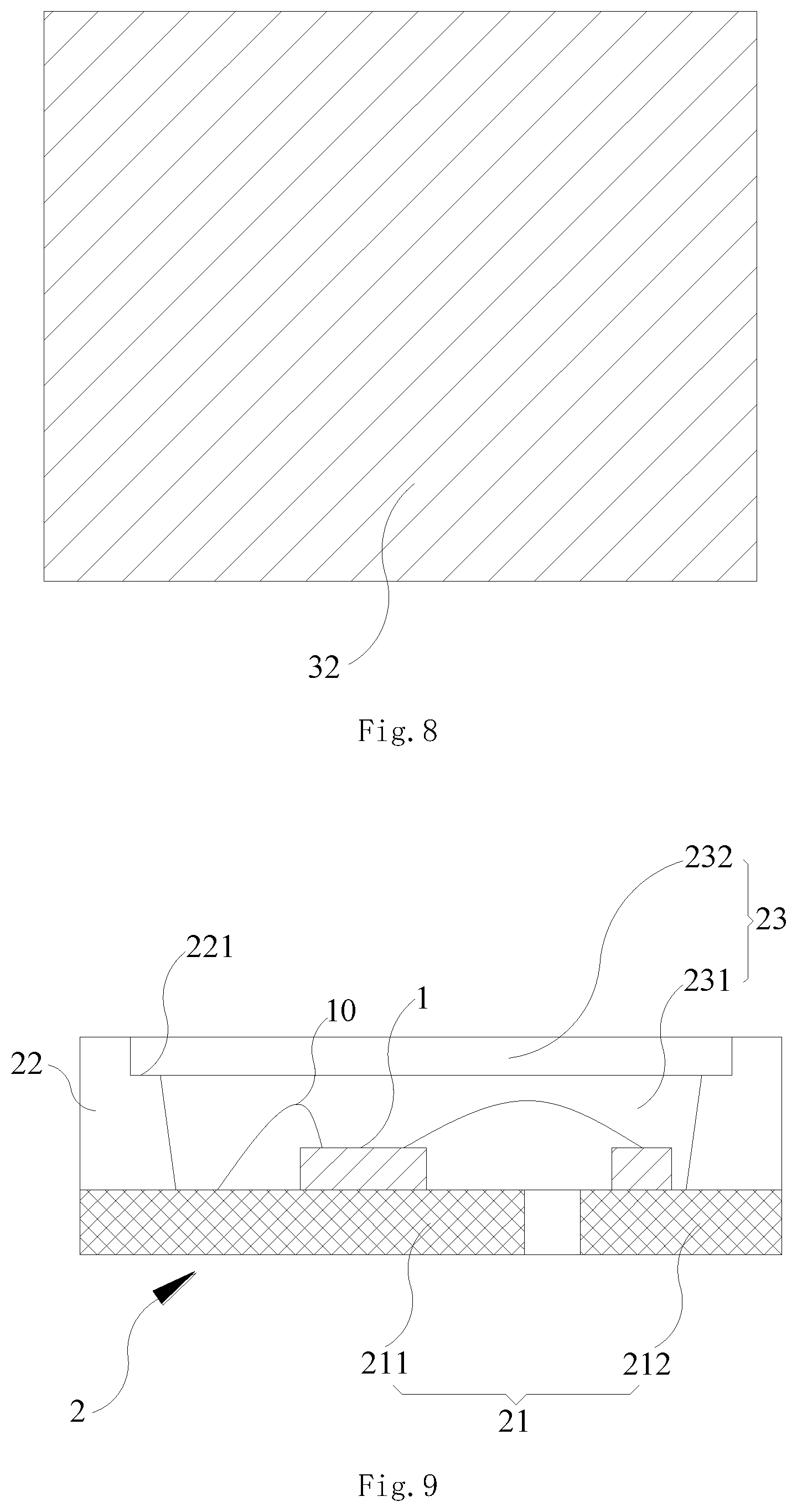
Please refer to FIG. 7 and FIG. 8, which illustrate another way to add the second fluorescent layer.
In this embodiment, the first fluorescent layer 31 is placed in the containing space 23. The top surface of the first fluorescent layer 31 is aligned with the top surface of the side walls 22. The second fluorescent layer 32 is placed upon the first fluorescent layer 31.
In this embodiment, the second side of the second fluorescent layer 32 has a curve surface. The angle between the first side and the second side of the second fluorescent layer 32 is smaller than 60 degrees.
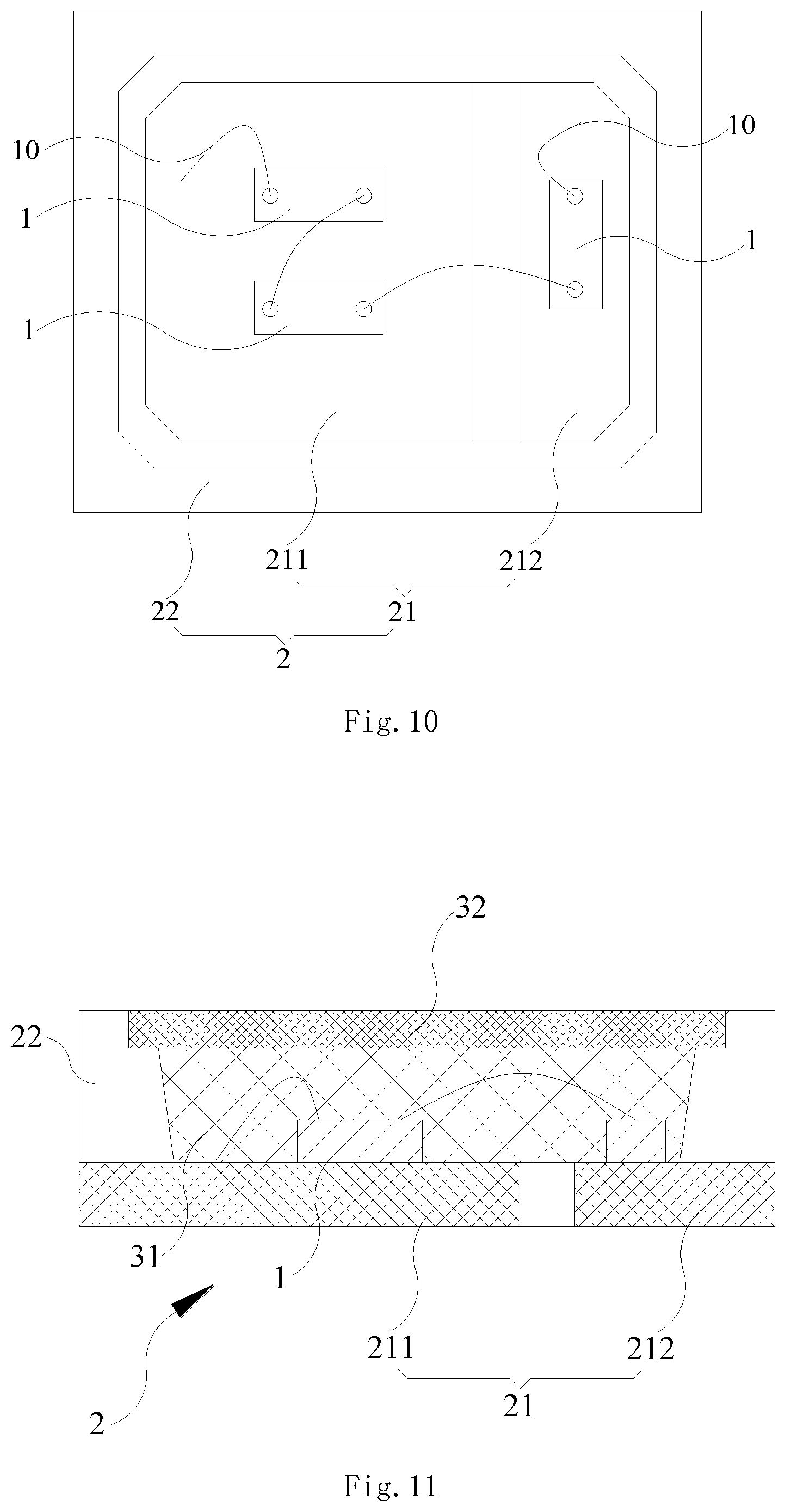
Please refer to FIG. 9 to FIG. 12.
In this embodiment, the side walls 22 have a ladder structure 221 for dividing the containing space 23 to a first containing space 231 and a second containing space 232.
The area of the second containing space 232 is larger than the area of the first containing space 231. The first fluorescent layer 31 is placed in the first containing space 231 and the second fluorescent layer 32 is placed in the second containing space 232.
Please refer to FIG. 13 and FIG. 14, which illustrate experimental results of such design.
FIG. 13 illustrate a conventional LED optical characteristic, while FIG. 14 illustrates optical characteristic of an example of the invention. It is clearly seen that the green light is well improved, which may increase overall CRI and luminous efficacy. Meanwhile, blue light is decreased to protect human eyes.
In addition to the above-described embodiments, various modifications may be made, and as long as it is within the spirit of the same invention, the various designs that can be made by those skilled in the art are belong to the scope of the present invention.
* * * * *
D00000
D00001
D00002
D00003
D00004
D00005
D00006
D00007
D00008
XML
uspto.report is an independent third-party trademark research tool that is not affiliated, endorsed, or sponsored by the United States Patent and Trademark Office (USPTO) or any other governmental organization. The information provided by uspto.report is based on publicly available data at the time of writing and is intended for informational purposes only.
While we strive to provide accurate and up-to-date information, we do not guarantee the accuracy, completeness, reliability, or suitability of the information displayed on this site. The use of this site is at your own risk. Any reliance you place on such information is therefore strictly at your own risk.
All official trademark data, including owner information, should be verified by visiting the official USPTO website at www.uspto.gov. This site is not intended to replace professional legal advice and should not be used as a substitute for consulting with a legal professional who is knowledgeable about trademark law.