Laser patterning of multi-layer structures
Dittli , et al. May 18, 2
U.S. patent number 11,008,644 [Application Number 16/141,504] was granted by the patent office on 2021-05-18 for laser patterning of multi-layer structures. This patent grant is currently assigned to nLIGHT, Inc.. The grantee listed for this patent is nLIGHT, Inc.. Invention is credited to Adam Dittli, Robert J. Martinsen.


| United States Patent | 11,008,644 |
| Dittli , et al. | May 18, 2021 |
Laser patterning of multi-layer structures
Abstract
A method of non-ablatively laser patterning a multi-layer structure, the multi-layer structure including a substrate, a first layer disposed on the substrate, a second layer disposed on the first layer, and a third layer disposed on the second layer, the method including generating at least one laser pulse having laser parameters selected for non-ablatively changing the conductivity a selected portion of the third layer such that the selected portion becomes non-conductive, and directing the pulse to the multi-layer structure, wherein the conductivity of the first layer is not substantially changed by the pulse.
| Inventors: | Dittli; Adam (Vancouver, WA), Martinsen; Robert J. (West Linn, OR) | ||||||||||
|---|---|---|---|---|---|---|---|---|---|---|---|
| Applicant: |
|
||||||||||
| Assignee: | nLIGHT, Inc. (Vancouver,
WA) |
||||||||||
| Family ID: | 51391874 | ||||||||||
| Appl. No.: | 16/141,504 | ||||||||||
| Filed: | September 25, 2018 |
Prior Publication Data
| Document Identifier | Publication Date | |
|---|---|---|
| US 20190032181 A1 | Jan 31, 2019 | |
Related U.S. Patent Documents
| Application Number | Filing Date | Patent Number | Issue Date | ||
|---|---|---|---|---|---|
| 14768613 | 10100393 | ||||
| PCT/US2014/017841 | Feb 21, 2014 | ||||
| 61767420 | Feb 21, 2013 | ||||
| 61818881 | May 2, 2013 | ||||
| 61875679 | Sep 9, 2013 | ||||
| Current U.S. Class: | 1/1 |
| Current CPC Class: | B82Y 40/00 (20130101); C22F 1/14 (20130101) |
| Current International Class: | C22F 1/14 (20060101); B82Y 40/00 (20110101) |
References Cited [Referenced By]
U.S. Patent Documents
| 3388461 | June 1968 | Lins |
| 4713518 | December 1987 | Yamazaki et al. |
| 4863538 | September 1989 | Deckard |
| 4953947 | September 1990 | Bhagavatula |
| 5008555 | April 1991 | Mundy |
| 5082349 | January 1992 | Cordova-Plaza et al. |
| 5231464 | July 1993 | Ichimura et al. |
| 5237150 | August 1993 | Karube |
| 5252991 | October 1993 | Storlie et al. |
| 5509597 | April 1996 | Laferriere |
| 5523543 | June 1996 | Hunter, Jr. et al. |
| 5566196 | October 1996 | Scifres |
| 5642198 | June 1997 | Long |
| 5719386 | February 1998 | Hsieh et al. |
| 5841465 | November 1998 | Fukunaga et al. |
| 5932119 | August 1999 | Kaplan et al. |
| 6310995 | October 2001 | Saini et al. |
| RE37585 | March 2002 | Mourou et al. |
| 6353203 | March 2002 | Hokodate et al. |
| 6362004 | March 2002 | Noblett |
| 6426840 | July 2002 | Partanen et al. |
| 6434302 | August 2002 | Fidric et al. |
| 6490376 | December 2002 | Au et al. |
| 6569382 | May 2003 | Edman et al. |
| 6577314 | June 2003 | Yoshida et al. |
| 7099535 | August 2006 | Bhagavatula et al. |
| 7151788 | December 2006 | Imakado et al. |
| 7218440 | May 2007 | Green |
| 7318450 | January 2008 | Nobili |
| 7349123 | March 2008 | Clarke et al. |
| 7622710 | November 2009 | Gluckstad |
| 7628865 | December 2009 | Singh |
| 7781778 | August 2010 | Moon et al. |
| 8071912 | December 2011 | Costin, Sr. et al. |
| 8237788 | August 2012 | Cooper et al. |
| 8251475 | August 2012 | Murray et al. |
| 8269108 | September 2012 | Kunishi et al. |
| 8288679 | October 2012 | Unrath |
| 8310009 | November 2012 | Saran et al. |
| 8404998 | March 2013 | Unrath et al. |
| 8414264 | April 2013 | Bolms et al. |
| 8415613 | April 2013 | Heyn et al. |
| 8442303 | May 2013 | Cheng et al. |
| 8472099 | June 2013 | Fujino et al. |
| 8809734 | August 2014 | Cordingley et al. |
| 9496683 | November 2016 | Kanskar |
| 9537042 | January 2017 | Dittli et al. |
| 2001/0050364 | December 2001 | Tanaka et al. |
| 2002/0147394 | October 2002 | Ellingsen |
| 2003/0174387 | September 2003 | Eggleton et al. |
| 2003/0213998 | November 2003 | Hsu et al. |
| 2004/0031779 | February 2004 | Cahill et al. |
| 2004/0112634 | June 2004 | Tanaka et al. |
| 2004/0126059 | July 2004 | Bhagavatula et al. |
| 2004/0207936 | October 2004 | Yamamoto et al. |
| 2005/0168847 | August 2005 | Sasaki |
| 2005/0191017 | September 2005 | Croteau et al. |
| 2005/0233557 | October 2005 | Tanaka et al. |
| 2006/0275705 | December 2006 | Dorogy et al. |
| 2007/0026676 | February 2007 | Li et al. |
| 2007/0041083 | February 2007 | Di Teodoro et al. |
| 2007/0075060 | April 2007 | Shedlov et al. |
| 2007/0251543 | November 2007 | Singh |
| 2008/0154249 | June 2008 | Cao |
| 2008/0231939 | September 2008 | Gluckstad |
| 2008/0246024 | October 2008 | Touwslager et al. |
| 2009/0052849 | February 2009 | Lee et al. |
| 2009/0080472 | March 2009 | Yao et al. |
| 2009/0122377 | May 2009 | Wagner |
| 2009/0274833 | November 2009 | Li |
| 2009/0297140 | December 2009 | Heismann et al. |
| 2009/0314752 | December 2009 | Manens et al. |
| 2009/0324233 | December 2009 | Samartsev et al. |
| 2010/0025387 | February 2010 | Arai et al. |
| 2010/0116794 | May 2010 | Taido et al. |
| 2010/0225974 | September 2010 | Sandstrom |
| 2010/0230665 | September 2010 | Verschuren et al. |
| 2010/0251437 | September 2010 | Heyn et al. |
| 2010/0252543 | October 2010 | Manens et al. |
| 2010/0257641 | October 2010 | Perkins et al. |
| 2011/0080476 | April 2011 | Dinauer et al. |
| 2011/0127697 | June 2011 | Milne |
| 2011/0133365 | June 2011 | Ushimaru et al. |
| 2011/0187025 | August 2011 | Costin, Sr. |
| 2011/0243161 | October 2011 | Tucker et al. |
| 2011/0253668 | October 2011 | Winoto |
| 2011/0278277 | November 2011 | Stork Genannt Wersborg |
| 2011/0279826 | November 2011 | Miura et al. |
| 2011/0316029 | December 2011 | Maruyama et al. |
| 2012/0127097 | May 2012 | Gaynor et al. |
| 2012/0128294 | May 2012 | Voss et al. |
| 2012/0145685 | June 2012 | Ream et al. |
| 2012/0148823 | June 2012 | Chu |
| 2012/0156458 | June 2012 | Chu |
| 2012/0295071 | November 2012 | Sato |
| 2012/0301733 | November 2012 | Eckert et al. |
| 2012/0301737 | November 2012 | Labelle et al. |
| 2013/0005139 | January 2013 | Krasnov |
| 2013/0022754 | January 2013 | Bennett et al. |
| 2013/0023086 | January 2013 | Chikama et al. |
| 2013/0027648 | January 2013 | Moriwaki |
| 2013/0095260 | April 2013 | Bovatsek et al. |
| 2013/0134637 | May 2013 | Wiesner et al. |
| 2013/0228442 | September 2013 | Mohaptatra et al. |
| 2013/0299468 | November 2013 | Unrath et al. |
| 2014/0104618 | April 2014 | Potsaid et al. |
| 2014/0155873 | June 2014 | Bor |
| 2014/0259589 | September 2014 | Xu et al. |
| 2014/0263209 | September 2014 | Burris et al. |
| 2014/0271328 | September 2014 | Burris et al. |
| 2014/0319381 | October 2014 | Gross |
| 2014/0332254 | November 2014 | Pellerite |
| 2014/0333931 | November 2014 | Lu et al. |
| 2015/0165556 | June 2015 | Jones et al. |
| 2015/0270089 | September 2015 | Ghanea-Hercock |
| 2015/0314612 | November 2015 | Balasini et al. |
| 2015/0352664 | December 2015 | Errico et al. |
| 2016/0059354 | March 2016 | Sercel et al. |
| 2016/0114431 | April 2016 | Cheverton et al. |
| 2016/0158889 | June 2016 | Carter et al. |
| 2016/0187646 | June 2016 | Ehrmann |
| 2016/0294150 | October 2016 | Johnson |
| 2017/0120537 | May 2017 | DeMuth et al. |
| 1217030 | Aug 2005 | CN | |||
| 1926460 | Mar 2007 | CN | |||
| 1966224 | May 2007 | CN | |||
| 101836309 | Oct 2007 | CN | |||
| 101143405 | Mar 2008 | CN | |||
| 101303269 | Nov 2008 | CN | |||
| 101314196 | Dec 2008 | CN | |||
| 102448623 | Mar 2009 | CN | |||
| 101733561 | Jun 2010 | CN | |||
| 201783759 | Apr 2011 | CN | |||
| 102084282 | Jun 2011 | CN | |||
| 102176104 | Sep 2011 | CN | |||
| 102207618 | Oct 2011 | CN | |||
| 102301200 | Dec 2011 | CN | |||
| 102441740 | May 2012 | CN | |||
| 102549377 | Jul 2012 | CN | |||
| 102582274 | Jul 2019 | CN | |||
| 203 20 269 | Apr 2004 | DE | |||
| 202016004237 | Aug 2016 | DE | |||
| 2587564 | May 2013 | EP | |||
| 2642246 | Sep 2013 | EP | |||
| H02220314 | Sep 1990 | JP | |||
| 2006-106227 | Apr 2006 | JP | |||
| 2008-281395 | Nov 2008 | JP | |||
| 10-2011-0109957 | Oct 2011 | KR | |||
| 2008742 | Feb 1994 | RU | |||
| 2021881 | Oct 1994 | RU | |||
| 553430 | Sep 2003 | TW | |||
| 200633062 | Sep 2006 | TW | |||
| I271904 | Jan 2007 | TW | |||
| 200707466 | Feb 2007 | TW | |||
| 201307949 | Feb 2013 | TW | |||
| WO 1995/011100 | Apr 1995 | WO | |||
| WO 1995/011101 | Apr 1995 | WO | |||
| WO 2011/146407 | Nov 2011 | WO | |||
| WO 2012/102655 | Aug 2012 | WO | |||
Other References
|
Decision of Rejection from the Korean Intellectual Property Office for related Application No. 10-2015-7025813, 6 pages, dated Nov. 29, 2018. cited by applicant . Affine Transformation--from Wolfram MathWorld, http://mathworld.wolfram.com/AffineTransformation.html, downloaded Feb. 21, 2014, 2 pages. cited by applicant . Chung, "Solution-Processed Flexible Transparent Conductors Composed of Silver Nanowire Networks Embedded in Indium Tin Oxide Nanoparticle Matrices," Nano Research, 10 pages (Sep. 24, 2012). cited by applicant . First Office Action from Chinese Application No. 201410455972.X, dated Jan. 26, 2016, 21 pages (with English translation). cited by applicant . First Office Action from Chinese Application No. 201480019324.8, dated Apr. 5, 2017, 20 pages (with English translation). cited by applicant . Gardner, "Precision Photolithography on Flexible Substrates," http://azorescorp.com/downloads/Articles/AZORESFlexSubstrate.pdf (prior to Jan. 30, 2013). cited by applicant . Giannini et al., "Anticipating, measuring, and minimizing MEMS mirror scan error to improve laser scanning microscopy's speed and accuracy," PLOS ONE, 14 pages (Oct. 3, 2017). cited by applicant . Grigoriyants et al., "Tekhnologicheskie protsessy lazernoy obrabotki," Moscow, izdatelstvo MGTU im. N.E. Baumana, p. 334 (2006). cited by applicant . International Search Report and Written Opinion for International Application No. PCT/US2013/060470, 7 pages, dated Jan. 16, 2014. cited by applicant . International Search Report and Written Opinion for International Application No. PCT/US2014/017841, 5 pages, dated Jun. 5, 2014. cited by applicant . International Search Report and Written Opinion for International Application No. PCT/US2014/017836, 6 pages, dated Jun. 10, 2014. cited by applicant . International Search Report and Written Opinion for International Application No. PCT/US2016/063086, 6 pages, dated Mar. 23, 2017. cited by applicant . International Search Report and Written Opinion for International Application No. PCT/US2017/014182, 9 pages, dated Mar. 31, 2017. cited by applicant . International Search Report and Written Opinion for International Application No. PCT/US2018/026110, 12 pages, dated Aug. 8, 2018. cited by applicant . Java--Transform a triangle to another triangle--Stack Overflow, http://stackoverflow.com/questions/1114257/transform-a-triangle-to-anothe- r-triangle?1q=1, downloaded Feb. 21, 2014, 3 pages. cited by applicant . Kummer et al., "Method to quantify accuracy of position feedback signals of a three-dimensional two-photon laser-scanning microscope," Biomedical Optics Express, 6(10):3678-3693 (Sep. 1, 2015). cited by applicant . Notice of Preliminary Rejection from the Korean Intellectual Property Office for related Application No. 10-2015-7025813, dated Jun. 26, 2018, 18 pages. cited by applicant . Office Action for related Korea Application No. 10-2014-0120247, dated Oct. 18, 2017, 6 pages (with English translation). cited by applicant . Official Letter and Search Report from the Taiwan Intellectual Property Office for related Application No. 102139285, 21 pages, dated Jun. 13, 2016 (w/ English translation.). cited by applicant . Official Letter and Search Report from the Taiwan Intellectual Property Office for related Application No. 103106020, 21 pages, dated Apr. 20, 2016 (w/ Eng. translation.). cited by applicant . Official Letter and Search Report from the Taiwan Intellectual Property Office for related Application No. 102139285, 8 pages, dated Nov. 21, 2016 (w/ Eng. translation.). cited by applicant . Official Letter and Search Report from Taiwan Application No. 103130968, dated Dec. 20, 2016, 16 pages (w/ Eng. translation). cited by applicant . Official Letter and Search Report from Taiwan Application No. 103106020, dated Jun. 6, 2017, 7 pages (with English translation). cited by applicant . Official Action (w/English translation) for related Taiwan application No. 103130968 dated Jun. 7, 2017, 5 pages. cited by applicant . Office Action (no English translation) for related Chinese Application No. 201480022179.9, 5 pages, dated Mar. 30, 2017. cited by applicant . Office Action (w/ English translation) for related Chinese Application No. 201380075745.8, 21 pages, dated Jun. 2, 2017. cited by applicant . Office Action (w/ Eng. translation) for related Korea Application No. 10-2014-0120247, dated Apr. 14, 2017, 11 pages. cited by applicant . PCI-6110, Multifunction I/O Device, http.//www.ni.com/en-us-support/model.pci-6110.html, downloaded Dec. 15, 2017, 1 page. cited by applicant . Product Brochure entitled "3-Axis and High Power Scanning" by Cambridge Technology, 4 pages, downloaded Dec. 21, 2013. cited by applicant . Product Brochure supplement entitled "Theory of Operation" by Cambridge Technology, 2 pages, downloaded Dec. 21, 2013. cited by applicant . Search Report from the Taiwan Intellectual Property Office for related Application No. 102139285, dated Sep. 1, 2015 (w/ Eng. translation.). cited by applicant . Search Report from the Taiwan Intellectual Property Office for related Application No. 102139285, 10 pages, dated Sep. 4, 2017 (w/ English translation). cited by applicant . Second Office Action from Chinese Application No. 201410455972.X, dated Nov. 22, 2016, 22 pages (w/ English translation). cited by applicant . Second Office Action from Chinese Application No. 201480019324.8, dated Nov. 16, 2017, 21 pages (with English translation). cited by applicant . Second Office Action from Chinese Application No. 201380075745.8, dated Feb. 26, 2018, 6 pages (with English translation). cited by applicant . Third Office Action from Chinese Application No. 201480019324.8, dated Apr. 13, 2018, 8 pages (with English translation). cited by applicant . Website describing 3-Axis Laser Scanning Systems at http://www.camtech.com/index.php?option=com_content&view=article&id=131&I- temid=181, 4 pages, accessed Dec. 31, 2014. cited by applicant. |
Primary Examiner: Su; Xiaowei
Attorney, Agent or Firm: Klarquist Sparkman, LLP
Parent Case Text
CROSS REFERENCE TO RELATED APPLICATIONS
This application is a continuation of U.S. patent application Ser. No. 14/768,613, filed Aug. 18, 2015, which is a U.S. National Stage of International Application No. PCT/US2014/017841, filed Feb. 21, 2014, which was published in English under PCT Article 21(2), which in turn claims the benefit of U.S. Provisional Application Nos. 61/767,420 filed Feb. 21, 2013, 61/818,881 filed May 2, 2013, and 61/875,679 filed Sep. 9, 2013, all of which are incorporated herein by reference in their entirety.
Claims
We claim:
1. A multi-layer structure, comprising: a substrate; a first layer situated on the substrate and having a conductive first portion and a non-conductive second portion adjacent the conductive first portion; an insulating second layer situated on the first layer; and a silver nano-wire third layer situated on the insulating second layer and having a conductive first portion and a non-ablatively laser formed non-conductive second portion adjacent to the conductive first portion.
2. The multi-layer structure of claim 1, wherein the conductive first portion of the first layer has a higher laser pulse conductivity alteration threshold than the conductive first portion of the silver nano-wire third layer.
3. The multi-layer structure of claim 1, wherein the conductive first portion of the first layer is indium tin oxide (ITO) and the non-conductive second portion of the first layer is ablated ITO.
4. The multi-layer structure of claim 1, wherein the non-conductive second portion of the silver nano-wire third layer overlies the non-conductive second portion of the first layer.
5. The multi-layer structure of claim 1, wherein the first layer includes silver nanowires.
6. The multi-layer structure of claim 1, wherein the insulating second layer comprises photoresist.
7. The multi-layer structure of claim 1, wherein the insulating second layer is situated to protect the first layer from a change in conductivity during non-ablative laser processing of the third layer.
8. The multi-layer structure of claim 7, wherein the second layer is situated to scatter or absorb energy during the non-ablative laser processing of the third layer.
9. The multi-layer structure of claim 1, wherein the first layer comprises a heat-treated layer.
10. The multi-layer structure of claim 9, wherein the heat-treated layer has a higher laser pulse conductivity altering threshold, relative to a laser pulse conductivity altering threshold of the conductive first portion of the silver nano-wire third layer, based on the heat treatment.
11. The multi-layer structure of claim 1, wherein the substrate comprises a substrate layer of polyethylene terephthalate (PET).
12. A touch-sensitive screen, comprising the multi-layer structure of claim 1.
13. A touch-sensitive sensor, comprising the multi-layer structure of claim 1.
14. The multi-layer structure of claim 1, wherein conductive first portion of the silver nano-wire third layer has a sheet resistance from 30-250 .OMEGA./sq.
15. The multi-layer structure of claim 1, wherein non-conductive second portion of the silver nano-wire third layer has a sheet resistance greater than or equal to about 20 M.OMEGA./sq.
16. The multi-layer structure of claim 1, wherein the conductive first portion and non-conductive second portion of the silver nano-wire third layer have a same surface roughness.
17. The multi-layer structure of claim 1, wherein to an unaided eye of an observer the conductive first portion and non-conductive second portion of the silver nano-wire third layer are visibly indistinguishable from each other.
18. The multi-layer structure of claim 1, wherein the conductive matrix of silver nanowires includes an organic overcoat.
Description
BACKGROUND OF THE INVENTION
1. Field of the Invention
Generally, the field of the present invention is laser patterning. More particularly, the present invention relates to methods for patterning multi-layer stackups of materials.
2. Background
Touch screens are gaining traction in the electronics industry due to the increasingly high demand for smartphones, tablet computers, and all-in-one computers. An industry objective has been to reduce the overall thickness of the device, so decreasing the touch sensor thickness is an integral part of obtaining thinner devices. One idea to reduce the sensor thickness is to use a single film. The single film is typically a layered composite structure that has more than one conductive film layers on the same substrate. The conductive layers are typically separated by a thin insulating material. Overall separation of the conductive layers is in the micron range. The small separation between layers has been problematic for patterning the layers, particularly as conventional laser techniques involve a large amount of heat for ablation of a selected layer which often introducing structural change to subsequent or adjacent layers. Accordingly, there remains a need for a laser patterning method that is at least capable of overcoming the attendant drawbacks of conventional techniques applied to multi-layer composites.
SUMMARY OF THE INVENTION
According to one aspect of the present invention, a method of laser patterning a multi-layer structure, the multi-layer structure including a substrate, a first layer disposed on the substrate, a second layer disposed on the first layer, and a third layer disposed on the second layer, the method includes generating at least one laser pulse having laser parameters selected for non-ablatively changing the conductivity a selected portion of the third layer such that the selected portion becomes non-conductive, and directing the pulse to the multi-layer structure, wherein the conductivity of the first layer is not substantially changed by the pulse.
In another aspect of the invention a method of forming a multi-layer stack-up structure, includes providing a substrate, depositing a first layer on the substrate, the first layer being conductive, laser patterning the first layer such that selected portions of the first layer become non-conductive, depositing a second layer on the first layer, the second layer being insulating, depositing a third layer on the second layer, the third layer being conductive, and non-ablatively laser patterning the third layer such that selected portions of the third layer become non-conductive without substantially changing the conductivity of the first layer.
The foregoing and other objects, features, and advantages will become more apparent from the following detailed description, which proceeds with reference to the accompanying figures.
BRIEF DESCRIPTION OF THE DRAWINGS
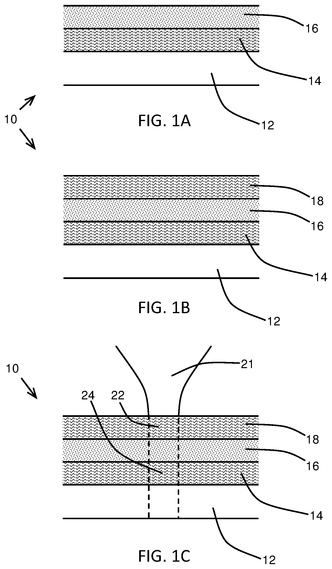
FIGS. 1A-1C show cross-sections of an exemplary stack-up structure at various steps in fabrication, in accordance with an aspect of the present invention.
FIGS. 2A-2C show cross-sections of an exemplary stack-up structure at various steps in fabrication, in accordance with another aspect of the present invention.
FIGS. 3A-3C show cross-sections of an exemplary stack-up structure at various steps in fabrication, in accordance with another aspect of the present invention.
DETAILED DESCRIPTION OF THE INVENTION
In general, the processes and materials discussed herein can be useful in touch sensor fabrication and other applications for conductive substrates. Touch sensors typically comprise a film composite of various materials which become stacked together through one or more deposition or lamination processes. A variety of stack-up configurations is possible, and various intermediate processing steps can be implemented during the fabrication of the multiple layers. For example, different multi-layer structures described herein can have layers arranged in a different order than as disclosed in the drawings. In some embodiments, deposited material layers can be disposed on one or both sides of a substrate. In further embodiments, the pulsed laser beam can be incident from the opposite direction as shown. Different types of materials can be used for the different layers, the ones being discussed herein being some suitable examples. It will be appreciated that many different configurations and variations are possible that are within the scope of the present invention.
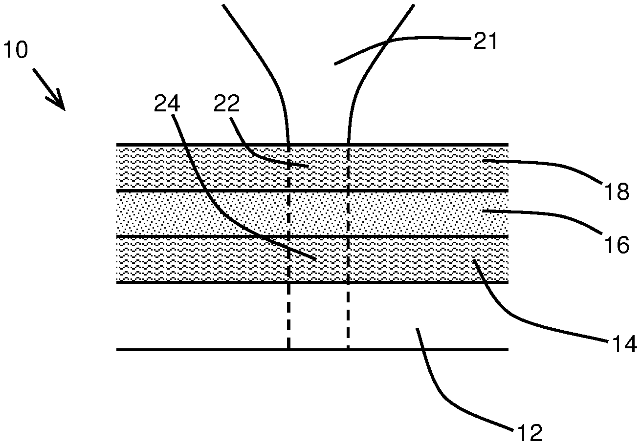
Reference is now made to FIGS. 1A-1C which depicts different stages for methods of non-ablative laser processing a multi-layer stack-up of materials, in accordance with aspects of the present invention. In FIG. 1A, a multi-layer stack-up structure 10 is provided which includes a substrate layer 12, made of PET or other suitable material. The structure 10 includes a conductive first layer 14 disposed on the substrate layer 12. The first layer 14 includes silver nanowires, or another suitable conductive material. A second layer 16, which may be made of photoresist or other suitable insulating material, is disposed on the first layer 14. Before the insulating layer 16 is deposited or formed on the first layer 14, the structure 10 can be laser processed non-ablatively to form selected non-conductive regions, including lines, patterns, or other geometries, the non-ablative processing being described further hereinafter.
The insulating layer 16 can include one or more dopants that increase the ability of the layer 16 to scatter or absorb incident laser energy so as to reduce the amount of residual fluence that is incident on the first layer 14. In FIG. 1B a third layer 18 is deposited or formed on the second layer 16 of the multi-layer structure 10. The third layer will typically include silver nanowires, though other suitable conductive materials can be used if capable of non-ablative conductivity alteration. One preferred layering is silver nanowires in both the first and third layers 14, 18. Silver nanowires offer several advantages over other materials, including the ability to be laser processed non-ablatively (as disclosed herein) and their ability to retain their characteristics under deformation, such as bending loads. For example, silver nanowires are well-suited for application in flexible touch screens. In FIG. 1C, a pulsed laser beam 21 is generated having process parameters suited for non-ablative alteration of the target. The pulsed laser beam 21 is directed to the structure 10 for laser processing of the structure 10. The pulsed beam 21 interacts with the third layer 18 of structure 10 without ablating a selected portion 22 of third layer 18. Through the interaction with the laser pulses from the pulsed laser beam 21 the conductivity of the selected portion 22 is changed to non-conductive. At the same time, a selected portion 24 of the first layer 14 that is below the third layer 18 does not experience the same change in conductivity. Additionally, the selected portion 24 is not ablated by the beam 21. The insulating layer 16 can assist in mitigating the pulse energy received by the first layer 14 in order to prevent a conductivity altering material interaction from occurring.
In FIGS. 2A-2C, another aspect is shown of a laser processing method of a multi-layer stack-up structure 20 in accordance with an aspect of the present invention. In FIG. 2A, a stack-up structure 20 includes a substrate 12 and a first layer 26, the first layer 26 preferably including silver nanowires. The first layer 26 is heat treated, represented by the downward facing arrows to alter upward a conductivity changing threshold characteristic of the first layer 26. Thus, after heat treatment, the threshold for alteration of the conductivity of the first layer 26 is higher. In some examples, this conductivity altering threshold can be related to an ablation threshold of the material. Various temperatures for heat treatment can be used and the temperature can be selected or adjusted to provide different effects to the first layer 26. In some examples heat treatment is performed with an oven, a laser, or other heat treating mechanism. The heat treatment of the first layer 26 can result in an alteration in density of an organic overcoat covering the silver nanowires in the first layer 26, increasing the fluence threshold thereof. In FIG. 2B, the structure 20 has undergone subsequent layering steps, providing second layer 16 on top of first layer 26, and a third layer 18 on top of second layer 16. In FIG. 2C, a pulsed laser beam 21 is generated having process parameters suited for non-ablative alteration of the target. The pulsed laser beam 21 is directed to the structure 20 for laser processing of the structure 20. The pulsed beam 21 interacts with the third layer 18 of structure 10 without ablating a selected portion 22 of third layer 18. Through the interaction with the laser pulses from the pulsed laser beam 21 the conductivity of the selected portion 22 is changed to non-conductive. At the same time, a selected portion 24 of the first layer 26 that is below the third layer 18 does not experience the same change in conductivity. Additionally, the selected portion 24 is not ablated by the beam 21.
With reference to FIGS. 3A-3C, an aspect is shown of a laser processing method of a multi-layer stack-up structure 30 in accordance with an aspect of the present invention. In FIG. 3A, a stack-up structure 30 includes a substrate 12 and a first layer 28, the first layer 28 preferably including indium tin oxide. The first layer 28 can be processed ablatively such that portions of the first layer 28 are removed through an ablative laser process. A second layer 16 is deposited on the first layer 28. In FIG. 3B a third layer 28 is deposited or formed on the second layer 16. Third layer 28 is different from the material composition of the first layer 28, with third layer 28 preferably includes conductive silver nanowires. Because of the material difference, the third layer 18 has a conductivity changing threshold characteristic that is different from the first layer 28. The structure 30 is processed by a pulsed laser beam 21 in FIG. 2C. The pulsed laser beam 21 is generated having process parameters suited for non-ablative alteration of the target. The pulsed laser beam 21 is directed to the structure 30 for laser processing of the structure 30. The pulsed beam 21 interacts with the third layer 18 of structure 10 without ablating a selected portion 22 thereof. Through the interaction with the laser pulses from the pulsed laser beam 21 the conductivity of the selected portion 22 is changed to non-conductive. At the same time, a selected portion 24 of the first layer 28 that is below the third layer 18 does not experience the same change in conductivity. Additionally, the selected portion 24 is not ablated by the beam 21.
Conductive regions or layers are processed non-ablatively so they can be used in a touch-sensitive screen in electronic devices or in other devices related to printed electronics or optoelectronics, including devices benefitting from low damage, low visibility processing of substrates or where precision is required. As used herein, ablative processing is understood to mean substantial removal of material from a target caused by an incident optical beam by vaporization, photochemical alteration, or otherwise. Similarly, non-ablative processing is understood to mean that the structural features of the existing target surface topology remain intact after processing, even if electrical or other properties of the target are changed.
In some cases, the layers of conductive materials include a random arrangement of silver nanowires. The silver nanowires of such layers can be secured to a substrate in a polymer matrix, such as an organic overcoat. A laser beam can deliver laser pulses to such a layer and create a processed portion where the conductivity of the material of conductive layer is substantially changed such that the processed portion is effectively non-conducting. As used herein, the terms "conductive" and "nonconductive" have meanings attributed to them that are generally understood in the art of printed electronics, touch sensor patterning, or optoelectronics. For example, suitable sheet resistances for a material such that it may be considered conductive include 30-250 .OMEGA./sq, and suitable sheet resistances or electrical isolation measurements for a material such that the material may be considered non-conductive or electrically isolated include resistances greater than or equal to about 20 M.OMEGA./sq. However, these sheet resistances are merely examples, and other conductive and non-conductive ranges may apply depending on the requirements of the particular application. Some processed substrates may be considered sufficiently conductive with sheet resistances below 500 .OMEGA./sq, 1 k.OMEGA./sq, 5 k.OMEGA./sq, or 10 k.OMEGA./sq, and may be considered non-conductive with sheet resistances greater than or equal to about 100 k.OMEGA./sq, 1 M.OMEGA./sq, or 100 M.OMEGA./sq.
Laser pulses can be directed to the composite in various patterns such that particular regions and electrical pathways are formed on the substrate. By carefully selecting the characteristics of the laser pulse parameters, including pulse length, pulse fluence, pulse energy, spot size, pulse repetition rate, and scan speed, the substrate may be processed such that electrical characteristics thereof are altered in a predetermined way while the substrate and associated protective and conductive layers are not substantially damaged or structurally altered (e.g., ablatively).
Exemplary laser pulse parameters suitable for non-ablative processing of a conductive layer include a pulse length of about 50 ps, pulse fluence of about 0.17 J/cm.sup.2, a spot size of about 40 .mu.m (1/e.sup.2), a scan rate of about 1 m/s with a pulse-to-pulse overlap of greater than 90%, a total pulse energy of about 12 .mu.J, and a pulse repetition rate of about 100 kHz, using optical radiation having a wavelength of 1064 nm (which has been found to interact with the substrate and other materials to a lesser extent than light of shorter wavelengths). Various other parameters are also suitable. For example, pulse repetition rates can be increased to 1 MHz, to 10 MHz, or to greater than 10 MHz to increase processing speeds. Pulse length can be selected to be shorter or longer. Pulse fluence can be adjusted to ensure that the target is processed non-ablatively. Possible pulse lengths include less than about 1 ps, 100 ps, 200 ps, 500 ps, 800 ps, or 1 ns. Other parameters can similarly be varied and optimized accordingly. Laser parameters suitable for non-ablative laser processing can be selected based in part on the relevant properties of the materials selected to be processed. For example, varying thickness of the substrate, the conductive layer, etc., can affect how laser pulse heat is distributed or result in other time-dependent effects requiring mitigation.
While beams for processing are generally brought to a focus at the structure, other beam geometrical configurations and intensity distributions are possible, including an unfocused beam, line beams, square or rectangular beams, as well as beams with uniform, substantially uniform or preselected intensity profiles across one or more transverse axes. In some cases, a composite can be translated to help achieve geometrical features on its surface. In some cases, one or more laser beams impinge on a composite from either a top or back side direction so that the beam propagates through the substrate to the conductive layer such that the beam causes ablative or non-ablative changes to a conductive layer. In some cases, laser pulses cause a processed portion of a conductive layer to become non-conductive without changing the visible characteristics of the processed portion. Similarly, laser pulses can process a conductive border either ablatively or non-ablatively. Laser ablation of a conductive border can be achieved by increasing the energy content of the laser beam incident on the target surface. For example, the laser pulse parameters can be adjusted by increasing the pulse length, pulse fluence, total pulse energy, by using shorter wavelengths, or by decreasing the spot size. Suitable laser systems capable generally include pulsed fiber lasers, pulsed fiber amplifiers, and diode pumped solid-state lasers.
It is thought that the present invention and many of the attendant advantages thereof will be understood from the foregoing description and it will be apparent that various changes may be made in the parts thereof without departing from the spirit and scope of the invention or sacrificing all of its material advantages, the forms hereinbefore described being merely exemplary embodiments thereof.
* * * * *
References
D00000
D00001
D00002
D00003
XML
uspto.report is an independent third-party trademark research tool that is not affiliated, endorsed, or sponsored by the United States Patent and Trademark Office (USPTO) or any other governmental organization. The information provided by uspto.report is based on publicly available data at the time of writing and is intended for informational purposes only.
While we strive to provide accurate and up-to-date information, we do not guarantee the accuracy, completeness, reliability, or suitability of the information displayed on this site. The use of this site is at your own risk. Any reliance you place on such information is therefore strictly at your own risk.
All official trademark data, including owner information, should be verified by visiting the official USPTO website at www.uspto.gov. This site is not intended to replace professional legal advice and should not be used as a substitute for consulting with a legal professional who is knowledgeable about trademark law.