Switchable image capturing system
Chang , et al. May 11, 2
U.S. patent number 11,003,042 [Application Number 16/287,291] was granted by the patent office on 2021-05-11 for switchable image capturing system. This patent grant is currently assigned to Ability Opto-Electronics Technology Co., Ltd.. The grantee listed for this patent is Ability Opto-Electronics Technology Co. Ltd.. Invention is credited to Yeong-Ming Chang, Chien-Hsun Lai, Yao-Wei Liu.


View All Diagrams
| United States Patent | 11,003,042 |
| Chang , et al. | May 11, 2021 |
Switchable image capturing system
Abstract
A switchable image capturing system is provided. Through modulating light by an electro-optical switch, the light intake received by the lens assembly and the image sensor may be changed. Specifically, when the electro-optical switch receives a positive voltage, the electro-optical switch obstructs the light so that the lens assembly and the image sensor are not able to image by receiving the light; when the electro-optical switch receives a negative voltage, the electro-optical switch allows the light to pass through so that the lens assembly and the image sensor is able to image by receiving the light. Through the configuration in the aforementioned statements, the image time of the image sensor may be controlled to interrupt or continue filming according to the user's needs.
| Inventors: | Chang; Yeong-Ming (Taichung, TW), Lai; Chien-Hsun (Taichung, TW), Liu; Yao-Wei (Taichung, TW) | ||||||||||
|---|---|---|---|---|---|---|---|---|---|---|---|
| Applicant: |
|
||||||||||
| Assignee: | Ability Opto-Electronics Technology
Co., Ltd. (Taichung, TW) |
||||||||||
| Family ID: | 68051234 | ||||||||||
| Appl. No.: | 16/287,291 | ||||||||||
| Filed: | February 27, 2019 |
Prior Publication Data
| Document Identifier | Publication Date | |
|---|---|---|
| US 20200026140 A1 | Jan 23, 2020 | |
Related U.S. Patent Documents
| Application Number | Filing Date | Patent Number | Issue Date | ||
|---|---|---|---|---|---|
| 62699268 | Jul 17, 2018 | ||||
| Current U.S. Class: | 1/1 |
| Current CPC Class: | G02F 1/155 (20130101); G02F 1/1514 (20190101); G02F 1/163 (20130101); G02B 9/12 (20130101); H04N 5/2254 (20130101); G02B 13/004 (20130101); G02B 13/0035 (20130101); G03B 11/04 (20130101); G02B 9/60 (20130101); G02B 13/0075 (20130101); G02F 1/157 (20130101); G02B 9/34 (20130101); G02B 13/0045 (20130101); H04N 5/23203 (20130101); H04N 5/238 (20130101); G02F 1/1524 (20190101); G02B 5/208 (20130101); G02F 1/133512 (20130101); G02F 1/1516 (20190101); G02F 2001/1552 (20130101); G03B 11/00 (20130101); G02F 1/133528 (20130101); G02F 2201/44 (20130101); G02F 1/1339 (20130101) |
| Current International Class: | G02F 1/163 (20060101); G03B 11/04 (20210101); G02F 1/1514 (20190101); G02B 13/00 (20060101); G02B 9/12 (20060101); G02B 9/34 (20060101); G02B 9/60 (20060101); G02F 1/157 (20060101); H04N 5/232 (20060101); H04N 5/225 (20060101); G02F 1/155 (20060101); G03B 11/00 (20210101); G02F 1/1335 (20060101); G02F 1/1516 (20190101); G02B 5/20 (20060101); G02F 1/1339 (20060101); G02F 1/1524 (20190101) |
References Cited [Referenced By]
U.S. Patent Documents
| 9930263 | March 2018 | Terasawa |
| 2001/0005283 | June 2001 | Osawa |
| 2001/0017985 | August 2001 | Tsuboi |
| 2008/0197371 | August 2008 | Ottermann |
| 2008/0231765 | September 2008 | Horiguchi |
| 2011/0102565 | May 2011 | Wang |
| 201205139 | Feb 2012 | TW | |||
Other References
|
Notice of Office Action of corresponding TW application, published on Jan. 16, 2020. cited by applicant. |
Primary Examiner: Lam; Hung H
Attorney, Agent or Firm: Wang Law Firm, Inc.
Parent Case Text
CROSS-REFERENCE TO RELATED APPLICATION
This application claims priority to and the benefit of, pursuant to 35 U.S.C. .sctn. 119, U.S. provisional patent application Ser. No. 62/699,268 filed on Jul. 17, 2018, the disclosure of which is incorporated herein in its entirety by reference.
Claims
What is claimed is:
1. A switchable image capturing system comprising: at least one image sensor positioned in a direction in which a light travels; at least one lens assembly positioned in the direction in which the light travels and in front of each of the image sensors, and an optical axis of the lens assembly overlapping a central normal line of a sensing surface of the image sensors in such a way that the light focuses on the image sensor; at least one electro-optical switch positioned in the direction in which the light travels, and each of the electro-optical switches changing a transmission rate thereof according to a control signal to obstruct a travel route of the light or to make the light pass through each of the electro-optical switches; and a microcontroller electrically connected to each of the electro-optical switches; wherein each of the electro-optical switches comprises a first substrate, a first transparent conductive layer, an auxiliary electrode layer, an electrolyte layer, an electrochromic layer, a second transparent conductive layer, and a second substrate; the first transparent conductive layer is disposed on the first substrate, the auxiliary electrode layer is disposed on the first transparent conductive layer, the electrolyte layer is disposed on the auxiliary electrode layer, the electrochromic layer is disposed on the electrolyte layer, the second transparent conductive layer is disposed on the electrochromic layer, and the second substrate is disposed on the second transparent conductive layer.
2. The switchable image capturing system according to claim 1, the microcontroller sends the control signal to each of the electro-optical switches according to a user command.
3. The switchable image capturing system according to claim 2, the microcontroller sends the control signal having a first voltage to each of the electro-optical switches according to the user command, and each of the electro-optical switches decreases a transmission rate thereof to obstruct a travel route of the light.
4. The switchable image capturing system according to claim 2, the microcontroller sends the control signal having a second voltage to each of the electro-optical switches according to the user command, and each of the electro-optical switches increases the transmission rate thereof to make the light pass through each of the electro-optical switches.
5. The switchable image capturing system according to claim 1, wherein a placement position of each of the electro-optical switches is perpendicular to the direction in which the light travels.
6. The switchable image capturing system according to claim 1, wherein each of the electro-optical switches is positioned in front of each of the lens assemblies, and the first substrate and the second substrate are positioned at a side adjacent to the lens assembly.
7. The switchable image capturing system according to claim 1, wherein each of the electro-optical switches is positioned between each of is lens assemblies and each of the image sensors, and the first substrate and the second substrate are positioned at a side adjacent to the lens assembly.
8. The switchable image capturing system according to claim 1, wherein each of the electro-optical switches is positioned between two lenses adjacent to each of the lens assemblies.
9. The switchable image capturing system according to claim 1, wherein each of the electro-optical switches further comprises a sealing structure; the sealing structure is disposed between the first substrate and the second substrate and surrounds the auxiliary electrode layer, the electrolyte layer, and the electrochromic layer.
10. The switchable image capturing system according to claim 1, wherein materials of the electrochromic layer are selected from a group consisting of at least one of transition metal oxide, an intercalated compound, an organic compound, and any combination thereof.
11. The switchable image capturing system according to claim 1, wherein each of the electro-optical switches comprises a first substrate, a first transparent conductive layer, a light-shielding layer, a second transparent conductive layer, and a second substrate; the first transparent conductive layer is disposed on the first substrate, the light-shielding layer is disposed on the first transparent conductive layer, the second transparent conductive layer is disposed on the light-shielding layer, and the second substrate is disposed on the second transparent conductive layer.
12. The switchable image capturing system according to claim 11, wherein a placement position of each of the electro-optical switches is perpendicular to the direction in which the light travels.
13. The switchable image capturing system according to claim 11, wherein each of the electro-optical switches is positioned in front of each of the lens assemblies, and the first substrate and the second substrate are positioned at a side adjacent to the lens assembly.
14. The switchable image capturing system according to claim 11, wherein each of the electro-optical switches is positioned between each of the lens assemblies and each of the image sensors, and the first substrate and the second substrate are positioned at the side adjacent to the lens assembly.
15. The switchable image capturing system according to claim 11, wherein each of the electro-optical switches is positioned between two lenses adjacent to each of the lens assemblies.
16. The switchable image capturing system according to claim 11, wherein each of the electro-optical switches further comprises a sealing structure; the sealing structure is disposed between the first substrate and the second substrate and surrounds the light-shielding layer.
17. The switchable image capturing system according to claim 11, wherein materials of the light-shielding layer comprise suspended particles and a polymer dispersed liquid crystal.
18. The switchable image capturing system according to claim 11, further comprising a polarizer, the polarizer disposed between the lens assembly and the electro-optical switch.
19. The switchable image capturing system according to claim 1, wherein each of the lens assemblies comprises three lenses having refractive power, which are a first lens, a second lens, and a third lens displayed sequentially from an object side to an image side; each of the lens assemblies satisfies the following conditions: 0.1.ltoreq.InTL/HOS.ltoreq.0.95; wherein, HOS is a distance from an object side surface of the first lens to an imaging surface of the image sensor on an optical axis; InTL is a distance from an object side surface of the first lens to an image side surface of the third lens on an optical axis.
20. The switchable image capturing system according to claim 1, wherein each of the lens assemblies comprises four lenses having refractive power, which are a first lens, a second lens, a third lens, and a fourth lens displayed sequentially from an object side to an image side; each of the lens assemblies satisfies the following conditions: 0.1.ltoreq.InTL/HOS.ltoreq.0.95; wherein, HOS is a distance from an object side surface of the first lens to the imaging surface of the image sensor on an optical axis; InTL is a distance from an object side surface of the first lens to an image side surface of the fourth lens on an optical axis.
21. The switchable image capturing system according to claim 1, wherein each of the lens assemblies comprises five lenses having refractive power, which are a first lens, a second lens, a third lens, a fourth lens, and a fifth lens displayed sequentially from an object side to an image side; each of the lens assemblies satisfies the following conditions: 0.1.ltoreq.InTL/HOS.ltoreq.0.95; wherein, HOS is a distance from an object side surface of the first lens to the imaging surface of the image sensor on an optical axis; InTL is a distance from an object side surface of the first lens to an image side surface of the fifth lens on an optical axis.
22. An image capturing system comprising the switchable image capturing system according to claim 1, wherein the switchable image capturing system is applied to and selected from the group consisting of at least one of an electronic portable device, an electronic wearable device, an electronic monitoring device, an electronic information device, an electronic communication device, a machine vision device, a vehicle electronic device, and any combination thereof.
Description
BACKGROUND OF THE INVENTION
1. Field of the Invention
The present invention relates to a switchable image capturing system which utilizes an electro-optical switch to control light intake in an attempt to control image capturing of an image sensor in a timely manner.
2. Description of the Related Art
Recently, 3C devices have been widely applied to countless uses and the scope to which Internet of Things (TOT) can be applied has also expanded by countless degrees. A user of 3C may be possibly recorded by an optical image capturing system, such as the front camera of a cell phone or a laptop, at any time. As a consequence, if the user needs security with mobility to keep privacy safe, it is essential to timely stop the optical image capturing system from continuing recording the user.
The conventional techniques use a mechanical lens cover to obstruct light routes, namely obstructing the object side of the lens with a lens cover. However, installing a lens cover not only seems redundant but also negatively affects the convenience of using the product. Thus, how to timely and conveniently interrupt the lens filming the user and the environment to secure the privacy of the user has become a critical issue which desperately needs to be addressed.
In view of the aforementioned statement, the inventor of the present invention has designed a switchable image capturing system in an effort to overcome deficiencies in terms of current techniques so as to enhance the implementation and application in industries.
SUMMARY OF THE INVENTION
In view of the aforementioned problems, the present invention aims to provide a switchable image capturing system to tackle with the issue encountered in prior art.
On the basis of the aforementioned purpose, the present invention provides a switchable image capturing system, including at least one image sensor, at least one lens assembly, at least one electro-optical switch, and a microcontroller. Each of the image sensors is positioned in a direction in which light travels. Each of the lens assemblies are positioned in the direction in which the light travels and in front of each of the image sensors, and an optical axis of the lens assembly overlaps a central normal line of a sensing surface of the image sensors in such a way that the light focuses on the image sensor. Each of the electro-optical switches is positioned in the direction in which the light travels and each of the electro-optical switches changes the transmission rate thereof according to a control signal to obstruct a travel route of the light or to make the light pass through each of the electro-optical switches. With the disposition of the electro-optical switches, the image time of the image sensor may be controlled to interrupt or continue filming according to the user's needs.
Preferably, the microcontroller of the present invention sends a control signal to each of the electro-optical switches according to the command of the user.
Preferably, the microcontroller sends a control signal having a first voltage to each of the electro-optical switches according to the user command, and each of the electro-optical switches decreases a transmission rate thereof to obstruct a travel route of the light.
Preferably, the microcontroller sends a control signal having a second voltage to each of the electro-optical switches according to the user command, and each of the electro-optical switches increases the transmission rate thereof to make the light pass through each of the electro-optical switches.
Preferably, each of the electro-optical switches comprises a first substrate, a first transparent conductive layer, an auxiliary electrode layer, an electrolyte layer, an electrochromic layer, a second transparent conductive layer, and a second substrate. The first transparent conductive layer is disposed on the first substrate. The auxiliary electrode layer is disposed on the first transparent conductive layer. The electrolyte layer is disposed on the auxiliary electrode layer. The electrochromic layer is disposed on the electrolyte layer. The second transparent conductive layer is disposed on the electrochromic layer. The second substrate is disposed on the second transparent conductive layer.
Preferably, the placement position of each of the electro-optical switches is perpendicular to the direction in which the light travels.
Preferably, each of the electro-optical switches is positioned in front of each of the lens assemblies, and the first substrate and the second substrate are positioned at a side adjacent to the lens assembly.
Preferably, each of the electro-optical switches is positioned between each of the lens assemblies and each of the image sensors, and the first substrate and the second substrate are positioned at a side adjacent to the lens assembly.
Preferably, each of the electro-optical switches is positioned between two lenses adjacent to each of the lens assemblies.
Preferably, each of the electro-optical switches further includes a sealing structure. The sealing structure is disposed between the first substrate and the second substrate and surrounds the auxiliary electrode layer, the electrolyte layer, and the electrochromic layer.
Preferably, materials of the electrochromic layer include a transition metal oxide, an intercalated compound, and an organic compound.
Preferably, each of the electro-optical switches includes a first substrate, a first transparent conductive layer, a light-shielding layer, a second transparent conductive layer, and a second substrate. The first transparent conductive layer is disposed on the first substrate. The light-shielding layer is disposed on the first transparent conductive layer. The second transparent conductive layer is disposed on the light-shielding layer. The second substrate is disposed on the second transparent conductive layer.
Preferably, the placement position of each of the electro-optical switches is perpendicular to the direction in which the light travels.
Preferably, each of the electro-optical switches is positioned in front of each of the lens assemblies, and the first substrate and the second substrate are positioned at a side adjacent to the lens assembly.
Preferably, each of the electro-optical switches is positioned between each of the lens assemblies and each of the image sensors, and the first substrate and the second substrate are positioned at a side adjacent to the lens assembly.
Preferably, each of the electro-optical switches is positioned between two lenses adjacent to each of the lens assemblies.
Preferably, each of the electro-optical switches further includes a sealing structure. The sealing structure is disposed between the first substrate and the second substrate and surrounds the light-shielding layer.
Preferably, materials of the light-shielding layer include suspended particles and a polymer dispersed liquid crystal.
Preferably, the switchable image capturing system of the present invention further includes a polarizer, and the polarizer is disposed between the lens assembly and the electro-optical switch.
Preferably, each of the lens assemblies includes three lenses having refractive power, which are a first lens, a second lens, and a third lens displayed sequentially from an object side to an image side. Each of the lens assemblies satisfies the following conditions: 0.1.ltoreq.InTL/HOS.ltoreq.0.95; wherein, HOS is the distance from an object side surface of the first lens to the sensing surface of the image sensor on an optical axis; InTL is the distance from an object side surface of the first lens to an image side surface of the third lens on an optical axis.
Preferably, each of the lens assemblies includes four lenses having refractive power, which are a first lens, a second lens, a third lens, and a fourth lens displayed sequentially from an object side to an image side. Each of the lens assemblies satisfies the following conditions: 0.1.ltoreq.InTL/HOS.ltoreq.0.95; wherein, HOS is the distance from an object side surface of the first lens to the sensing surface of the image sensor on an optical axis; InTL is the distance from an object side surface of the first lens to an image side surface of the fourth lens on an optical axis.
Preferably, each of the lens assemblies includes five lenses having refractive power, which are a first lens, a second lens, a third lens, a fourth lens, and a fifth lens displayed sequentially from an object side to an image side. Each of the lens assemblies satisfies the following conditions: 0.1.ltoreq.InTL/HOS.ltoreq.0.95; wherein, HOS is the distance from an object side surface of the first lens to the sensing surface of the image sensor on an optical axis; InTL is the distance from an object side surface of the first lens to an image side surface of the fifth lens on an optical axis.
On the basis of the aforementioned purposes, the switchable image capturing system of the present invention may be applied to electronic portable devices, electronic wearable devices, electronic monitoring devices, electronic information devices, electronic communication devices, machine vision devices, vehicle electronic devices, and any combination thereof.
Accordingly, for the switchable image capturing system of the present invention, the image time of the image sensor may be controlled via modulating the electro-optical switches to interrupt or continue filming according to the user's needs.
BRIEF DESCRIPTION OF THE DRAWINGS
FIG. 1 depicts a block diagram of the switchable image capturing system according to the present invention.
FIG. 2 depicts a schematic diagram of the electro-optical switch of the switchable image capturing system according to the first embodiment of the present invention.
FIG. 3 depicts a schematic diagram of the electro-optical switch of the switchable image capturing system according to the second embodiment of the present invention.
FIG. 4 depicts a configuration diagram of the switchable image capturing system according to the first embodiment of the present invention.
FIG. 5 depicts a configuration diagram of the switchable image capturing system according to the second embodiment of the present invention.
FIG. 6 depicts a configuration diagram of the switchable image capturing system according to the third embodiment of the present invention.
FIG. 7 depicts a configuration diagram of the lens assembly of the switchable image capturing system according to the first optical embodiment of the present invention.
FIG. 8 depicts a curve diagram of the spherical aberration, astigmatism, and optical distortion illustrated sequentially from the left to the right according to the first optical embodiment of the present invention.
FIG. 9 depicts a configuration diagram of the lens assembly of the switchable image capturing system according to the second optical embodiment of the present invention.
FIG. 10 depicts a curve diagram of the spherical aberration, astigmatism, and optical distortion illustrated sequentially from the left to the right according to the second optical embodiment of the present invention.
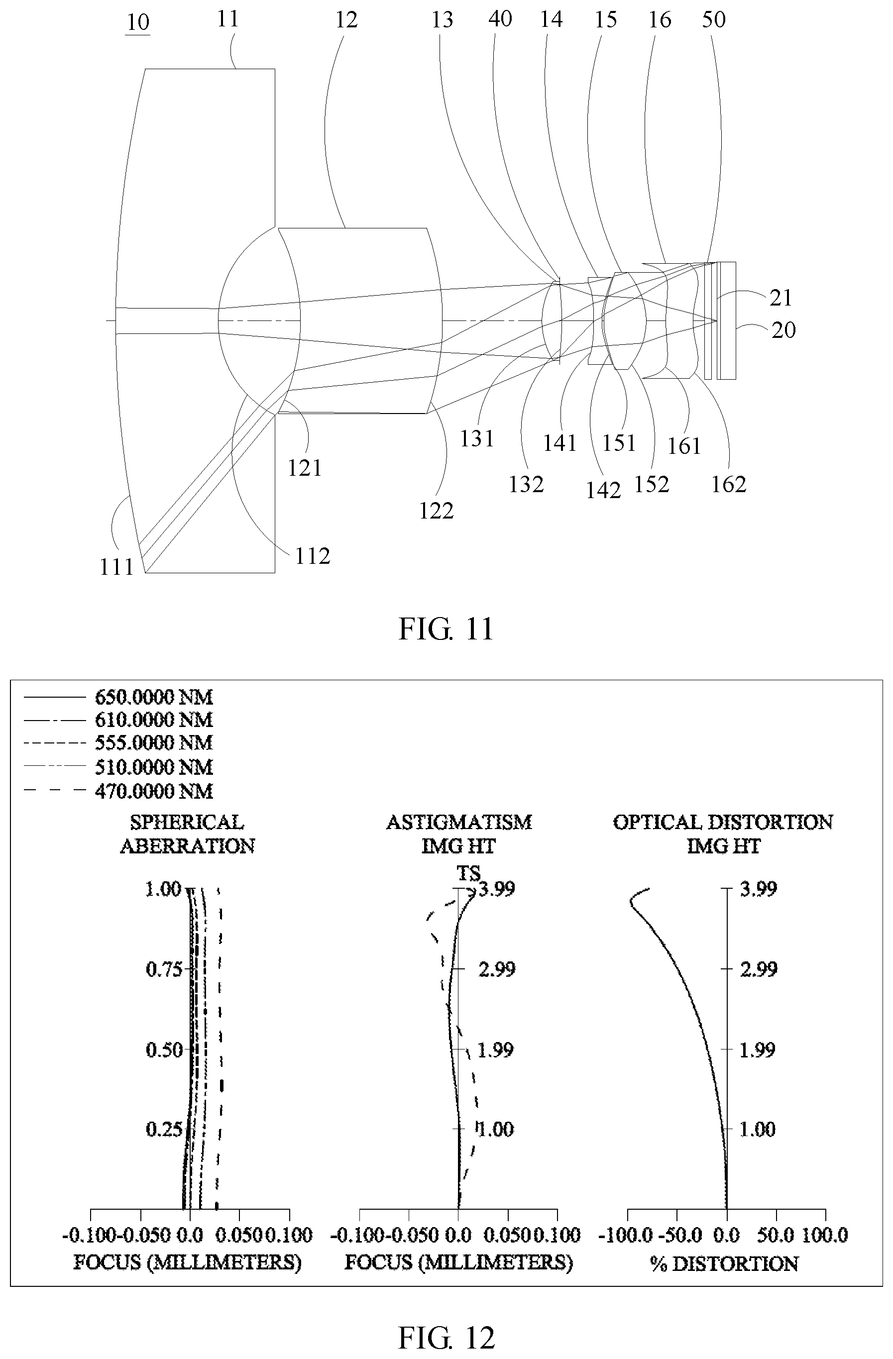
FIG. 11 depicts a configuration diagram of the lens assembly of the switchable image capturing system according to the third optical embodiment of the present invention.
FIG. 12 depicts a curve diagram of the spherical aberration, astigmatism, and optical distortion illustrated sequentially from the left to the right according to the third optical embodiment of the present invention.
FIG. 13 depicts a configuration diagram of the lens assembly of the switchable image capturing system according to the fourth optical embodiment of the present invention.
FIG. 14 depicts a curve diagram of the spherical aberration, astigmatism, and optical distortion illustrated sequentially from the left to the right according to the fourth optical embodiment of the present invention.
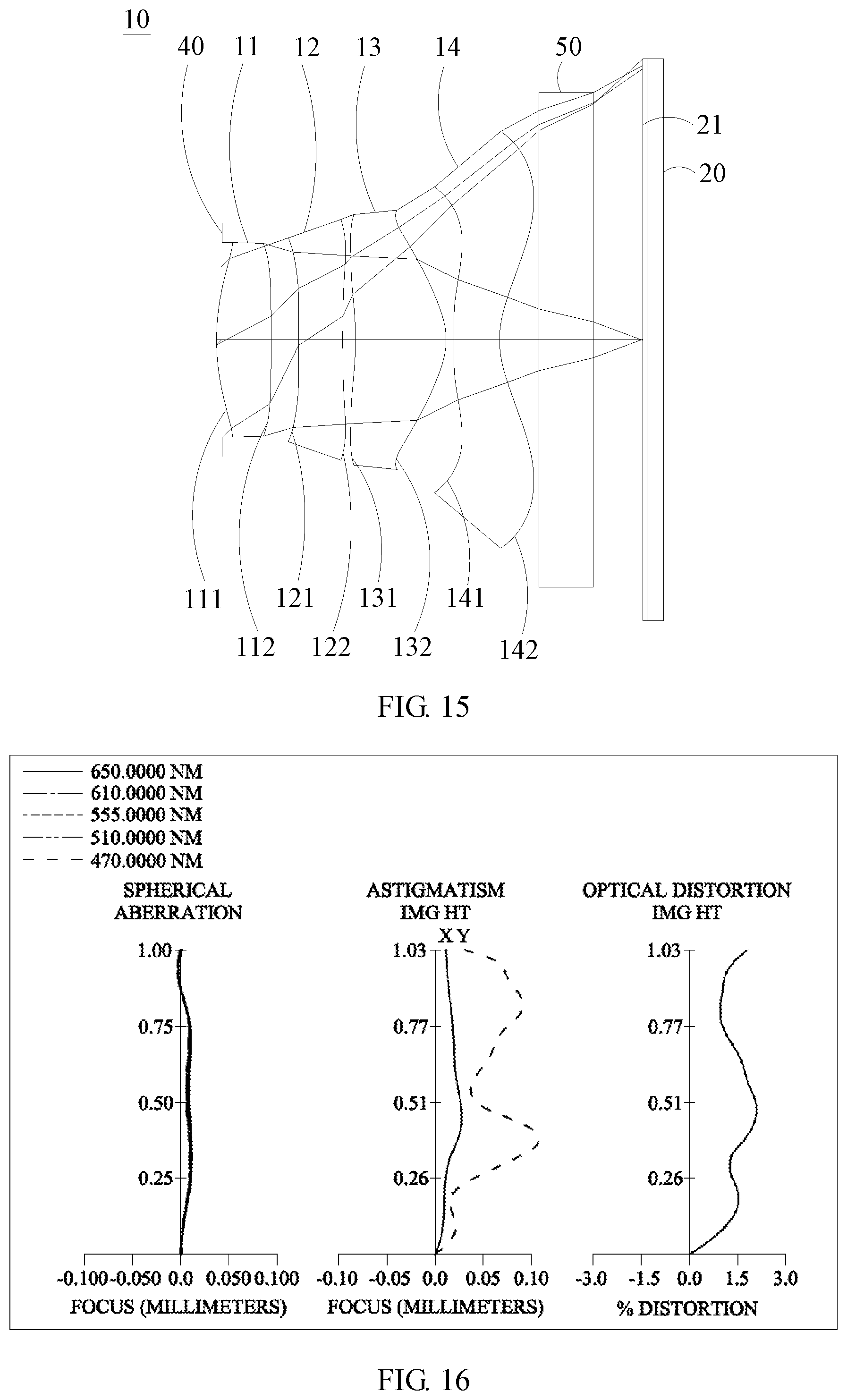
FIG. 15 depicts a configuration diagram of the lens assembly of the switchable image capturing system according to the fifth optical embodiment of the present invention.
FIG. 16 depicts a curve diagram of the spherical aberration, astigmatism, and optical distortion illustrated sequentially from the left to the right according to the fifth optical embodiment of the present invention.
FIG. 17 depicts a configuration diagram of the lens assembly of the switchable image capturing system according to the sixth optical embodiment of the present invention.
FIG. 18 depicts a curve diagram of the spherical aberration, astigmatism, and optical distortion illustrated sequentially from the left to the right according to the sixth optical embodiment of the present invention.
DESCRIPTION OF THE PREFERRED EMBODIMENTS
The advantages, features, and technical methods of the present invention are to be explained in detail with reference to the exemplary embodiments and the figures for the purpose of being more easily to be understood. Moreover, the present invention may be realized in different forms, and should not be construed as being limited to the embodiments set forth herein. Conversely, for a person skilled in the art, the embodiments provided shall make the present invention convey the scope more thoroughly, comprehensively, and completely. In addition, the present invention shall be defined only by the appended claims.
Please refer to FIG. 1, which depicts a block diagram of the switchable image capturing system according to the present invention. As shown in FIG. 1, the switchable image capturing system of the present invention includes at least one image sensor 20, at least one lens assembly 10, at least one electro-optical switch 30, and a microcontroller MCU. Each of the image sensors 20 is positioned in a direction in which light travels. Each of the lens assemblies 10 are positioned in the direction in which the light travels and in front of each of the image sensors 20, and an optical axis of the lens assembly 10 overlaps a central normal line of a sensing surface of the image sensors in such a way that the light focuses on the image sensor 20. Each of the electro-optical switches 30 is positioned in the direction in which the light travels and each of the electro-optical switches 30 changes the transmission rate thereof according to a control signal to obstruct a travel route of the light or to make the light pass through each of the electro-optical switches 30. The microcontroller MCU is electrically connected to each of the electro-optical switches 30 and sends the control signal to each of the electro-optical switches 30 according to a command of a user. With the disposition of the electro-optical switches 30, the image time of the image sensor 20 may be controlled and the filming of the image sensor 20 may be interrupted or continued according to the user's needs.
It should be noted that the number of the image sensors 20, the lens assemblies 10, and the electro-optical switches 30 are changed according to the user's needs and engineer needs for design. Hence, the number of the image sensors 20, the lens assemblies 10, and the electro-optical switches 30 are not limited herein.
Herein, the microcontroller MCU controlling each of the electro-optical switches 30 is explained in detail in the following steps: (1) When a user does not need to film with the image sensor 20, the user issues a user command to the microcontroller MCU. The microcontroller MCU sends a control signal having a first voltage to each of the electro-optical switches 30 according to the user command. The first voltage is a positive voltage, and each of the electro-optical switches 30 decreases a transmission rate thereof to obstruct a travel route of the light so that each of the image sensors 20 does not receive light, resulting in not performing filming and imaging. (2) When the user needs to film with the image sensor 20, the user issues a user command to the microcontroller MCU. The microcontroller MCU sends a control signal having a second voltage to each of the electro-optical switches 30 according to the user command. Each of the electro-optical switches 30 increases a transmission rate thereof to make the light pass through each of the electro-optical switches 30 so that each of the image sensors 20 receives light, resulting in performing filming and imaging. In addition, the value of the first voltage may also be adjusted according to the user's needs so that part of the light passes through each of the electro-optical switches 30 instead of completely obstructing the light entering each of the image sensors.
Please refer to FIG. 2, which depicts a schematic diagram of the electro-optical switch of the switchable image capturing system according to the first embodiment of the present invention. FIG. 2 (a) depicts a layer structural diagram of the electro-optical switch of the switchable image capturing system according to the first embodiment of the present invention. As shown in FIG. 2 (a), a single electro-optical switch of the present invention includes a first substrate 31, a first transparent conductive layer 32, an auxiliary electrode layer 33, an electrolyte layer 34, an electrochromic layer 35, a second transparent conductive layer 36, a second substrate 37, and a sealing structure 41. The first transparent conductive layer 32 is disposed on the first substrate 31. The auxiliary electrode layer 33 is disposed on the first transparent conductive layer 32. The electrolyte layer 34 is disposed on the auxiliary electrode layer 33. The electrochromic layer 35 is disposed on the electrolyte layer 34. The second transparent conductive layer 36 is disposed on the electrochromic layer 35. The second substrate 37 is disposed on the second transparent conductive layer 36. The sealing structure 41 is disposed between the first substrate 31 and the second substrate 37 and surrounds the auxiliary electrode layer 33, the electrolyte layer 34, and the electrochromic layer 35 in an attempt to prevent the solution in the electrolyte layer 34 from flowing out. FIG. 2 (b) depicts a cross-section diagram of the electro-optical switch of the switchable image capturing system according to the first embodiment of the present invention. As shown in FIG. 2 (b), U-shape electrodes 39 may be disposed on the electro-optical switch 30. The electrodes 39 may be formed by respectively cladding the end of the first substrate 31 and the first transparent conductive layer 32 as well as the end of the second substrate 31 and the second transparent conductive layer 36 by using metal foils. The microcontroller MCU may be electrically connected to the electrodes 39 via wires 40 so that voltage may be sent to the electro-optical switch 30. In an embodiment, the electrodes 39 may be formed outside of the sealing structure 41 without overlapping with the auxiliary electrode layer 33, the electrolyte layer 34, and the electrochromic layer 35. In another embodiment, the auxiliary electrode layer 33, the electrolyte layer 34, and the electrochromic layer 35 overlapping with the electrodes 39 may be activated.
Wherein, the setup of the electro-optical switch of the present invention is described as follows: The first substrate 31 and the second substrate 37 may be selected from one of a glass substrate, a quartz substrate, a sapphire substrate, and a silicon carbide (SiC) substrate. The material of the first transparent conductive layer 32 and the second transparent conductive layer 36 includes ITO, ZnO, AlGaInSnO, AZO, SnO.sub.2, In.sub.2O.sub.3, SnZnO, or graphene. The material of the auxiliary electrode layer 33 includes NiO.sub.x, Ni(OH).sub.2, or Co(OH).sub.2. The material of the electrolyte layer 34 includes electrolyte of salts including ZrO.sub.2, HfO.sub.2, Ta.sub.2O.sub.5, an oxide of SiO.sub.2, MgF.sub.2, and CeF.sub.3, or includes electrolyte of acids including LiClO.sub.4 or H.sub.3PO.sub.4 and organic macromolecules such as CPE (cross-linked polyether), PEO (poly (ethylene oxide)), PVA (poly (vinyl alcohol)), and PVP (poly (vinyl piperidine)). The material of the electrochromic layer 35 includes at least one selected from the group consisting of transition metal oxides, intercalated compounds, and organic compounds. The transition metal oxides include WO.sub.3, V.sub.2O.sub.5, NiO.sub.x, MoO.sub.3, Nb.sub.2O.sub.5, TiO.sub.2, or Rh.sub.2O.sub.3. The intercalated compounds include Fe.sub.4[Fe(CN).sub.6]3, Fe.sub.4[Ru(CN).sub.6].sub.3, CoFe(CN).sub.6, KVFe(CN).sub.6, or InFe(CN).sub.6. The organic compounds include pyrazoline, poly(aniline), and tetrathiafulvalene.
It should be noted that the electro-optical switch 30 according to the first embodiment of the present invention prompts oxidation-reduction reaction to occur by applying voltages to the electrochromic layer. The ions required for the oxidation-reduction are provided by the electrolyte layer 34. Specifically, when the electrochromic layer 35 undergoes a reduction reaction, the electrochromic layer 35 begins to change to a color such as blue, green, or yellow. The color of the electrochromic layer 35 is selected according to the aforementioned materials having various colors, thus achieving the purpose of obstructing light. When the electrochromic layer 35 undergoes an oxidation reaction, the electrochromic layer 35 begins to become transparent and colorless, which makes the visible light band penetrate the electrochromic layer 35, further allowing light to enter the image sensor 20.
It is worth mentioning that the electrochromic layer 35 can be different colors according to requirements, so the electro-optical switch 30 having the electrochromic layer 35 may be applied to a filter. For instance, the electrochromic layer 35 of the electro-optical switch 30 becomes green when a positive voltage is applied, with only the green light band (500 nm-550 nm) being allowed to pass through and preventing the light with other colors from passing through the electro-optical switch 30.
Please refer to FIG. 3, which depicts a schematic diagram of the electro-optical switch of the switchable image capturing system according to the second embodiment of the present invention. FIG. 3 (a) depicts a layer structural diagram of the electro-optical switch of the switchable image capturing system according to the second embodiment of the present invention. As shown in FIG. 3 (a), each of the single electro-optical switches 30 includes a first substrate 31, a first transparent conductive layer 32, a light-shielding layer 38, a second transparent conductive layer 36, a second substrate 37, and a sealing structure 41. The first transparent conductive layer 32 is disposed on the first substrate 31. The light-shielding layer 38 is disposed on the first transparent conductive layer 32. The second transparent conductive layer 36 is disposed on the light-shielding layer 38. The second substrate 37 is disposed on the second transparent conductive layer 36. The sealing structure 41 is disposed between the first substrate 31 and the second substrate 37 and surrounds the light-shielding layer 38 in an attempt to prevent the solution in the light-shielding layer 38 from flowing out. FIG. 3 (b) depicts a cross-section diagram of the electro-optical switch of the switchable image capturing system according to the second embodiment of the present invention. As shown in FIG. 3 (b), electrodes 39 may be disposed on the electro-optical switch 30. The electrodes 39 may be formed on the first transparent conductive layer 32 and second transparent conductive layer 36 in a form of a contact pad. The microcontroller MCU may be electrically connected to the electrodes 39 via wires 40 so that voltage may be sent to the electro-optical switch 30. The electrodes 39 may be formed on the first transparent conductive layer 32 and the second transparent conductive layer 36 by using metal materials, conductive adhesive, or other highly conductive materials collocated with the mesh electrode and the optical lithography patterning method. In an embodiment, the electrodes 39 may be formed outside of the sealing structure 41 without overlapping with the light-shielding layer 38. In another embodiment, the light-shielding layer 38 overlapping with the electrodes 39 may be activated. In an embodiment, the electrodes 39 may be manufactured by using metal materials, conductive adhesive, or other highly conductive materials collocated with the mesh electrode and the optical lithography patterning method.
Wherein, the material of the light-shielding layer 38 includes suspended particles and a polymer dispersed liquid crystal. Since the molecular arrangement direction of such material may be rotated when undertaking voltages, the purpose of obstructing light may be achieved. The auxiliary electrode layer 33 and the electrolyte layer 34 may therefore not be needed. Moreover, since the molecular arrangement direction of the light-shielding layer 38 may be rotated owing to voltages, making the light polarized, a polarizer may be disposed between the lens assembly 10 and the electro-optical switch 30 in such a way that the polarized angle of the light may be more diverse.
Please refer to FIG. 4, which depicts a configuration diagram of the switchable image capturing system according to the first embodiment of the present invention. As shown in FIG. 4, the lens assembly 10 is set with three lenses. The placement position of the electro-optical switch 30 is perpendicular to the direction in which the light travels. The electro-optical switch 30 is positioned in front of the lens assembly 10 and the first substrate 31 of the electro-optical switch 30 is positioned at a side adjacent to the lens assembly 10. The manner in which the electro-optical switch 30 is placed is not particularly limited, and only the electro-optical switch 30 is positioned in front of the lens assembly 10. In another embodiment, the second substrate 37 of the electro-optical switch 30 is positioned at a side adjacent to the lens assembly 10.
Please refer to FIG. 5, which depicts a configuration diagram of the switchable image capturing system according to the second embodiment of the present invention. As shown in FIG. 5, the lens assembly 10 is set with three lenses. The placement position of the electro-optical switch 30 is perpendicular to the direction in which the light travels. The electro-optical switch 30 is positioned between two lenses adjacent to each of the lens assemblies.
Please refer to FIG. 6, which depicts a configuration diagram of the switchable image capturing system according to the third embodiment of the present invention. As shown in FIG. 6, the lens assembly 10 is set with three lenses. The placement position of the electro-optical switch 30 is perpendicular to the direction in which the light travels. The electro-optical switch 30 is positioned between the lens assembly 10 and the image sensor 20. The first substrate 31 and the second substrate 37 of the electro-optical switch 30 may be positioned at a side adjacent to the lens assembly 10. The manner in which the electro-optical switch 30 is placed is not particularly limited, and only the electro-optical switch 30 is positioned in front of the lens assembly 10.
It should be noted that the configurations of FIGS. 4 to 6 are applicable to the electro-optical switches 30 of the first embodiment and the second embodiment. The manner in which each of the electro-optical switches 30 is placed may be selected from FIGS. 4 to 6. Each of the electro-optical switches 30 may be placed in the same as or different way from each other. That is, the manner in which each of the electro-optical switches 30 is placed may be the same or different. For instance, some electro-optical switches 30 are configured according to FIG. 4; another electro-optical switches 30 are configured according to FIG. 5; the other electro-optical switches 30 are configured according to FIG. 6. Each of the electro-optical switches 30 may be the electro-optical switch 30 of the first embodiment and the second embodiment. All of the electro-optical switches 30 are the electro-optical switch 30 of the first embodiment or the electro-optical switch 30 of the second embodiment. It also may be that some electro-optical switches 30 are the electro-optical switch 30 of the first embodiment, and the other electro-optical switch 30 is the electro-optical switch 30 of the second embodiment.
In some embodiments, the lens assembly 10 includes three lenses with refractive power, which are a first lens, a second lens, and a third lens sequentially displayed from an object side to an image side, and the lens assembly 10 satisfies the following condition: 0.1.ltoreq.InTL/HOS.ltoreq.0.95; wherein, HOS is a distance from an object side surface of the first lens to the image side surface on an optical axis; InTL is a distance from an object side surface of the first lens to an image side surface of the third lens on an optical axis.
In some embodiments, the lens assembly 10 includes four lenses with refractive power, which are a first lens, a second lens, a third lens, and a fourth lens sequentially displayed from an object side to an image side, and the lens assembly 10 satisfies the following condition: 0.1.ltoreq.InTL/HOS.ltoreq.0.95; wherein, HOS is a distance from an object side surface of the first lens to the image side surface on an optical axis; InTL is a distance from an object side surface of the first lens to an image side surface of the fourth lens on an optical axis.
In some embodiments, the lens assembly 10 includes five lenses with refractive power, which are a first lens, a second lens, a third lens, a four lens, and a fifth lens sequentially displayed from an object side to an image side, and the lens assembly 10 satisfies the following condition: 0.1.ltoreq.InTL/HOS.ltoreq.0.95; wherein, HOS is a distance from an object side surface of the first lens to the image side surface on an optical axis; InTL is a distance from an object side surface of the first lens to an image side surface of the fifth lens on an optical axis.
In addition to the structural embodiment as mentioned above, an optical embodiment related to the lens assembly 10 is to be described as follows. The switchable image capturing system of the present invention may be designed using three operational wavelengths, namely 486.1 nm, 587.5 nm, and 656.2 nm. Wherein, 587.5 nm is the main reference wavelength for the technical features. The switchable image capturing system of the present invention may be designed using five operational wavelengths, namely 470 nm, 510 nm, 555 nm, 610 nm 650 nm. Wherein, 555 nm is the main reference wavelength for the technical features.
PPR is the ratio of the focal length f of the lens assembly 10 to a focal length fp of each of lenses with positive refractive power. NPR is the ratio of the focal length f of the lens assembly 10 to the focal length fn of each of lenses with negative refractive power. The sum of the PPR of all the lenses with positive refractive power is .SIGMA.PPR. The sum of the NPR of all the lenses with negative refractive power is .SIGMA.NPR. Controlling the total refractive power and total length of the lens assembly 10 may be achieved when the following conditions are satisfied: 0.5.ltoreq..SIGMA.PPR/|.SIGMA.NPR.ltoreq.15. Preferably, the following conditions may be satisfied: 1.ltoreq..SIGMA.PPR/|.ltoreq.NPR|3.0.
In addition, HOI is defined as half a diagonal of a sensing field of the image sensor 20 (i.e., the imaging height or the maximum imaging height of the switchable image capturing system). HOS is a distance on the optical axis from an object side of the first lens to the image plane, which satisfies the following conditions: HOS/HOI.ltoreq.50; and 0.5.ltoreq.HOS/f.ltoreq.150. Preferably, the following conditions are satisfied: 1.ltoreq.HOS/HOI.ltoreq.40; 1.ltoreq.HOS/f.ltoreq.140. Therefore, the switchable image capturing system may be maintained in miniaturization so that the module may be equipped on thin and portable electronic products.
In addition, in an embodiment, at least one aperture may be disposed in the lens assembly 10 of the present invention to reduce stray light and enhance image quality.
Specifically, the disposition of the aperture may be a front aperture or a middle aperture in the lens assembly 10 of the present invention. Wherein, the front aperture is the aperture disposed between the shot object and the first lens. The front aperture is the aperture disposed between the first lens and the image plane. If the aperture is the front aperture, a longer distance may be created between the exit pupil and the image plane in the lens assembly 10 so that more optical elements may be accommodated and the efficiency of image sensor elements receiving images may be increased. If the aperture is the middle aperture, the field of view of the system may be expended in such a way that the optical image capturing module has the advantages of a wide-angle lens. InS is defined as the distance from the aforementioned aperture to the image plane, which satisfies the following condition: 0.1.ltoreq.InS/HOS.ltoreq.1.1. Therefore, the features of the lens assembly 10 maintained in miniaturization and having wide-angle may be attended simultaneously.
In the lens assembly 10 of the present invention, InTL is a distance on the optical axis from an object side of the first lens to an image side surface of the sixth lens. .SIGMA.TP is the sum of the thicknesses of all the lenses with refractive power on the optical axis. The following conditions are satisfied: 0.1.ltoreq..SIGMA.TP/InTL.ltoreq.0.9. Therefore, the contrast ratio of system imaging and the yield rate of lens manufacturing may be attended simultaneously. Moreover, an appropriate back focal length is provided to accommodate other elements.
R1 is the curvature radius of the object side surface of the first lens. R2 is the curvature radius of the image side surface of the first lens. The following condition is satisfied: 0.001.ltoreq.|R1/R2|.ltoreq.25. Therefore, the first lens is equipped with appropriate intensity of positive refractive power to prevent the spherical aberration from increasing too fast. Preferably, the following condition is satisfied: 0.01.ltoreq.|R1/R2|<12.
R11 is the curvature radius of the object side surface of the sixth lens. R12 is the curvature radius of the image side surface of the sixth lens. This following condition is satisfied: -7<(R11-R12)/(R11+R12)<50. Therefore, it is advantageous to correct the astigmatism generated by the lens assembly 10.
IN12 is the distance between the first lens and the second lens on the optical axis. The following condition is satisfied: IN12/f.ltoreq.60. Therefore, it is beneficial to improve the chromatic aberration of the lenses so as to enhance the performance.
IN56 is the distance between the fifth lens and the sixth lens on the optical axis. The following condition is satisfied: IN56/f.ltoreq.3.0. Therefore, it is beneficial to improve the chromatic aberration of the lens so as to enhance the performance.
TP1 and TP2 are respectively the thicknesses of the first lens and the second lens on the optical axis. The following condition is satisfied: 0.1.ltoreq.(TP1+IN12)/TP2.ltoreq.10. Therefore, it is beneficial to control the sensitivity produced by the optical image capturing module so as to enhance the performance.
TP5 and TP6 are respectively the thicknesses of the fifth lens and the sixth lens on the optical axis. The following condition is satisfied: 0.1.ltoreq.(TP6+IN56)/TP5.ltoreq.15. Therefore, it is beneficial to control the sensitivity produced by the optical image capturing module so as to enhance the performance.
TP2, TP3, and TP4 are respectively the thicknesses of the second lens, the third lens, and the fourth lens on the optical axis. IN23 is the distance between the second lens and the third lens on the optical axis. IN45 is the distance between the third lens and the fourth lens on the optical axis. InTL is the distance from an object side surface of the first lens to an image side surface of the sixth lens. The following condition is satisfied: 0.1.ltoreq.TP4/(IN34+TP4+IN45)<1. Therefore, it is beneficial to slightly correct the aberration generated by the incident light advancing in the process layer upon layer so as to decrease the overall height of the system.
In the lens assembly 10, HVT61 is the distance perpendicular to the optical axis between a critical point C61 on an object side surface of the sixth lens and the optical axis. HVT62 is the distance perpendicular to the optical axis between a critical point C62 on an image side surface of the sixth lens and the optical axis. SGC61 is a distance parallel to the optical axis from an axial point on the object side surface of the sixth lens to the critical point C61. SGC62 is the distance parallel to the optical axis from an axial point on the image side surface of the sixth lens to the critical point C62. The following conditions may be satisfied: 0 mm.ltoreq.HVT61.ltoreq.3 mm; 0 mm<HVT62.ltoreq.6 mm; 0.ltoreq.HVT61/HVT62; 0 mm.ltoreq.|SGC61|.ltoreq.0.5 mm; 0 mm<|SGC62|.ltoreq.2 mm; and 0<|SGC62|/(|SGC62|+TP6).ltoreq.0.9. Therefore, it may be effective to correct the aberration of the off-axis view field.
The lens assembly 10 of the present invention satisfies the following condition: 0.2.ltoreq.HVT62/HOI.ltoreq.0.9. Preferably, the following condition may be satisfied: 0.3.ltoreq.HVT62/HOI.ltoreq.0.8. Therefore, it is beneficial to correct the aberration of the surrounding view field of the lens assembly 10.
The lens assembly 10 of the present invention satisfies the following condition: 0.ltoreq.HVT62/HOS.ltoreq.0.5. Preferably, the following condition may be satisfied: 0.2.ltoreq.HVT62/HOS.ltoreq.0.45. Hereby, it is beneficial to correct the aberration of the surrounding view field of the lens assembly 10.
In the lens assembly 10 of the present invention, SGI611 denotes a distance parallel to an optical axis from an inflection point on the object side surface of the sixth lens which is nearest to the optical axis to an axial point on the object side surface of the sixth lens. SGI621 denotes a distance parallel to an optical axis from an inflection point on the image side surface of the sixth lens which is nearest to the optical axis to an axial point on the image side surface of the sixth lens. The following condition are satisfied: 0<SGI611/(SGI611+TP6).ltoreq.0.9; 0<SGI621/(SGI621+TP6).ltoreq.0.9. Preferably, the following conditions may be satisfied: 0.1.ltoreq.SGI611/(SGI611+TP6).ltoreq.0.6; 0.1.ltoreq.SGI621/(SGI621+TP6).ltoreq.0.6.
SGI612 denotes a distance parallel to the optical axis from the inflection point on the object side surface of the sixth lens which is the second nearest to the optical axis to an axial point on the object side surface of the sixth lens. SGI622 denotes a distance parallel to an optical axis from an inflection point on the image side surface of the sixth lens which is the second nearest to the optical axis to an axial point on the image side surface of the sixth lens. The following conditions are satisfied: 0<SGI612/(SGI612+TP6).ltoreq.0.9; 0<SGI622/(SGI622+TP6).ltoreq.0.9. Preferably, the following conditions may be satisfied: 0.1.ltoreq.SGI612/(SGI612+TP6).ltoreq.0.6; 0.1.ltoreq.SGI622/(SGI622+TP6).ltoreq.0.6.
HIF611 denotes the distance perpendicular to the optical axis between the inflection point on the object side surface of the sixth lens which is the nearest to the optical axis and the optical axis. HIF621 denotes the distance perpendicular to the optical axis between an axial point on the image side surface of the sixth lens 16 and an inflection point on the image side surface of the sixth lens which is the nearest to the optical axis. The following conditions are satisfied: 0.001 mm.ltoreq.|HIF611|.ltoreq.5 mm; 0.001 mm.ltoreq.|HIF621|.ltoreq.5 mm. Preferably, the following conditions may be satisfied: 0.1 mm.ltoreq.|HIF611|.ltoreq.3.5 mm; 1.5 mm.ltoreq.|HIF621|.ltoreq.3.5 mm.
HIF612 denotes the distance perpendicular to the optical axis between the inflection point on the object side surface of the sixth lens which is the second nearest to the optical axis and the optical axis. HIF622 denotes the distance perpendicular to the optical axis between an axial point on the image side surface of the sixth lens and an inflection point on the image side surface of the sixth lens which is the second nearest to the optical axis. The following conditions are satisfied: 0.001 mm.ltoreq.|HIF612|.ltoreq.5 mm; 0.001 mm.ltoreq.|HIF622|.ltoreq.5 mm. Preferably, the following conditions may be satisfied: 0.1 mm.ltoreq.|HIF622|.ltoreq.3.5 mm; 0.1 mm.ltoreq.|HIF612|.ltoreq.3.5 mm.
HIF613 denotes the distance perpendicular to the optical axis between the inflection point on the object side surface of the sixth lens which is the third nearest to the optical axis and the optical axis. HIF623 denotes the distance perpendicular to the optical axis between an axial point on the image side surface of the sixth lens and an inflection point on the image side surface of the sixth lens which is the third nearest to the optical axis. The following conditions are satisfied: 0.001 mm.ltoreq.|HIF613|.ltoreq.5 mm; 0.001 mm.ltoreq.|HIF623|.ltoreq.5 mm. Preferably, the following conditions may be satisfied: 0.1 mm.ltoreq.|HIF623|.ltoreq.3.5 mm; 0.1 mm.ltoreq.|HIF613|.ltoreq.3.5 mm.
HIF614 denotes the distance perpendicular to the optical axis between the inflection point on the object side surface of the sixth lens which is the fourth nearest to the optical axis and the optical axis. HIF624 denotes the distance perpendicular to the optical axis between an axial point on the image side surface of the sixth lens and an inflection point on the image side surface of the sixth lens which is the fourth nearest to the optical axis. The following conditions are satisfied: 0.001 mm.ltoreq.|HIF614|.ltoreq.5 mm; 0.001 mm.ltoreq.|HIF624|.ltoreq.5 mm. Preferably, the following relations may be satisfied: 0.1 mm.ltoreq.|HIF624|.ltoreq.3.5 mm and 0.1 mm.ltoreq.|HIF614|.ltoreq.3.5 mm.
In the lens assembly 10 of the present invention, (TH1+TH2)/HOI satisfies the following condition: 0<(TH1+TH2)/HOI.ltoreq.0.95, or 0<(TH1+TH2)/HOT.ltoreq.0.5 preferably. (TH1+TH2)/HOS satisfies the following condition: 0<(TH1+TH2)/HOS.ltoreq.0.95, or 0<(TH1+TH2)/HOS.ltoreq.0.5 preferably. 2*(TH1+TH2)/PhiA satisfies the following condition: 0<2*(TH1+TH2)/PhiA.ltoreq.0.95, or 0<2*(TH1+TH2)/PhiA.ltoreq.0.5 preferably.
In an embodiment of the lens assembly 10 in the present invention, interchangeably arranging the lenses with a high dispersion coefficient and a low dispersion coefficient is beneficial to correcting the chromatic aberration of lens assembly 10.
The equation for the aspheric surface as mentioned above is: z=ch2/[1+[1(k+1)c2h2]0.5]+A4h4+A6h6+A8h8+A10h10+A12h12+A14h14+A16h16+A18h- 18+A20h20+ . . . (1)
Wherein, z is a position value of the position along the optical axis at the height h where the surface apex is regarded as a reference; k is the conic coefficient; c is the reciprocal of curvature radius; and A4, A6, A8, A10, A12, A14, A16, A18, and A20 are high order aspheric coefficients.
In the lens assembly 10 of the present invention, the material of the lens may be made of glass or plastic. Using plastic as the material for producing the lens may effectively reduce the cost of manufacturing. In addition, using glass as the material for producing the lens may control the heat effect and increase the designed space configured by the refractive power of the optical image capturing module. Moreover, the object side surface and the image side surface from the first lens 11 to the sixth lens 17 may be aspheric, which may obtain more control variables. Apart from eliminating the aberration, the number of lenses used may be reduced compared with that of traditional lenses used made by glass. Thus, the total height of the lens assembly 10 may be reduced effectively.
Furthermore, in the lens assembly 10 of the present invention, when the surface of the lens is a convex surface, the surface of the lens adjacent to the optical axis is convex in principle. When the surface of the lens is a concave surface, the surface of the lens adjacent to the optical axis is concave in principle.
In the lens assembly 10 of the present invention, at least one of the first lens, the second lens, the third lens, the fourth lens, the fifth lens, and sixth lens may further be designed as a light filtration element with a wavelength of less than 500 nm depending on requirements. The light filtration element may be realized by coating at least one surface of the specific lens with the filter function, or may be realized by the lens itself having the material capable of filtering short wavelength.
The image plane of the lens assembly 10 of the present invention may be a plane or a curved surface depending requirements. When the image plane is a curved surface such as a spherical surface with a curvature radius, the incident angle necessary for focusing light on the image plane may be reduced. Hence, it not only contributes to shortening the length (TTL) of the optical image capturing module, but also promotes the relative illuminance.
The First Optical Embodiment
As shown in FIG. 7, the lens assembly 10 includes six lenses with refractive power, which are a first lens 11, a second lens 21, a third lens 13, a four lens 14, a fifth lens 15, and a sixth lens 16.
Please refer to FIG. 7 and FIG. 8. FIG. 7 depicts a configuration diagram of the lens assembly of the switchable image capturing system according to the first embodiment of the present invention. FIG. 8 is a curve diagram of the spherical aberration, astigmatism, and optical distortion illustrated sequentially from the left to the right according to the first optical embodiment of the present invention. As shown in FIG. 7, the switchable image capturing system includes a first lens 11, an aperture 40, a second lens 12, a third lens 13, a four lens 14, a fifth lens 15, a sixth lens 16, an IR-cut filter 50, an image plane 21, and image sensor elements 20 sequentially displayed from an object side to an image side.
The first lens 11 has negative refractive power and is made of a plastic material. The object side surface 111 thereof is a concave surface and the image side surface 112 thereof is a concave surface, both of which are aspheric. The object side surface 111 thereof has two inflection points. ARS11 denotes the arc length of the maximum effective half diameter of the object side surface 111 of the first lens 11. ARS12 denotes the arc length of the maximum effective half diameter of the image side surface 112 of the first lens 11. ARE11 denotes the arc length of half the entrance pupil diameter (HEP) of the object side surface 111 of the first lens 11. ARE12 denotes the arc length of half the entrance pupil diameter (HEP) of the image side surface 112 of the first lens 11. TP1 is the thickness of the first lens 11 on the optical axis.
SGI111 denotes a distance parallel to the optical axis from the inflection point on the object side surface 111 of the first lens 11 which is the nearest to the optical axis to an axial point on the object side surface 111 of the first lens 11. SGI121 denotes a distance parallel to an optical axis from an inflection point on the image side surface 112 of the first lens 11 which is the nearest to the optical axis to an axial point on the image side surface 112 of the first lens 11. The following conditions are satisfied: SGI111=-0.0031 mm; |SGI111|/(|SGI111|+TP1)=0.0016.
SGI112 denotes the distance parallel to the optical axis from the inflection point on the object side surface 111 of the first lens 11 which is the second nearest to the optical axis to an axial point on the object side surface 111 of the first lens 11. SGI122 denotes the distance parallel to an optical axis from an inflection point on the image side surface 112 of the first lens 11 which is the second nearest to the optical axis to an axial point on the image side surface 112 of the first lens 11. The following conditions are satisfied: SGI112=1.3178 mm; SGI112/(SGI112+TP1)=0.4052.
HIF111 denotes the distance perpendicular to the optical axis between the inflection point on the object side surface 111 of the first lens 11 which is the nearest to the optical axis and the optical axis. HIF121 denotes the distance perpendicular to the optical axis between an axial point on the image side surface 112 of the first lens 11 and an inflection point on the image side surface 112 of the first lens 11 which is the nearest to the optical axis. The following conditions are satisfied: HIF111=0.5557 mm; HIF111/HOI=0.1111.
HIF112 denotes the distance perpendicular to the optical axis between the inflection point on the object side surface 111 of the first lens 11 which is the second nearest to the optical axis and the optical axis. HIF122 denotes the distance perpendicular to the optical axis between an axial point on the image side surface 112 of the first lens 11 and an inflection point on the image side surface 112 of the first lens 11 which is the second nearest to the optical axis. The following conditions are satisfied: HIF112=5.3732 mm; HIF112/HOI=1.0746.
The second lens 12 has positive refractive power and is made of a plastic material. The object side surface 121 thereof is a convex surface and the image side surface 122 thereof is a convex surface, both of which are aspheric. The object side surface 121 thereof has an inflection point. ARS21 denotes the arc length of the maximum effective half diameter of the object side surface 121 of the second lens 12. ARS22 denotes the arc length of the maximum effective half diameter of the image side surface 122 of the second lens 12. ARE21 denotes an arc length of half the entrance pupil diameter (HEP) of the object side surface 121 of the second lens 12. ARE22 denotes the arc length of half the entrance pupil diameter (HEP) of the image side surface 122 of the second lens 12. TP2 is the thickness of the second lens 12 on the optical axis.
SGI211 denotes the distance parallel to the optical axis from the inflection point on the object side surface 121 of the second lens 12 which is the nearest to the optical axis to an axial point on the object side surface 121 of the second lens 12. SGI221 denotes the distance parallel to an optical axis from an inflection point on the image side surface 122 of the second lens 12 which is the nearest to the optical axis to an axial point on the image side surface 122 of the second lens 12. The following conditions are satisfied: SGI211=0.1069 mm; SGI211/(SGI211+TP2)=0.0412; SGI221=0 mm; SGI221/(SGI221+TP2)=0.
HIF211 denotes the distance perpendicular to the optical axis between the inflection point on the object side surface 121 of the second lens 12 which is the nearest to the optical axis and the optical axis. HIF221 denotes the distance perpendicular to the optical axis between an axial point on the image side surface 122 of the second lens 12 and an inflection point on the image side surface 122 of the second lens 12 which is the nearest to the optical axis. The following conditions are satisfied: HIF211=1.1264 mm; HIF211/HOI=0.2253; HIF221=0 mm; HIF221/HOI=0.
The third lens 13 has negative refractive power and is made of a plastic material. The object side surface 131 thereof is a concave surface and the image side surface 132 thereof is a convex surface, both of which are aspheric. The object side surface 131 and the image side surface 132 thereof both have an inflection point. ARS31 denotes the arc length of the maximum effective half diameter of the object side surface 131 of the third lens 13. ARS32 denotes an arc length of the maximum effective half diameter of the image side surface 132 of the third lens 13. ARE31 denotes the arc length of half the entrance pupil diameter (HEP) of the object side surface 131 of the third lens 13. ARE32 denotes the arc length of half the entrance pupil diameter (HEP) of the image side surface 132 of the third lens 13. TP3 is the thickness of the third lens 13 on the optical axis.
SGI311 denotes the distance parallel to the optical axis from the inflection point on the object side surface 131 of the third lens 13 which is the nearest to the optical axis to an axial point on the object side surface 131 of the third lens 13. SGI321 denotes the distance parallel to an optical axis from an inflection point on the image side surface 132 of the third lens 13 which is the nearest to the optical axis to an axial point on the image side surface 132 of the third lens 13. The following conditions are satisfied: SGI311=-0.3041 mm; |SGI311|/(|SGI311|+TP3)=0.4445; SGI321=-0.1172 mm; |SGI321|/(|SGI321|+TP3)=0.2357.
HIF311 denotes the distance perpendicular to the optical axis between the inflection point on the object side surface 131 of the third lens 13 which is the nearest to the optical axis and the optical axis. HIF321 denotes the distance perpendicular to the optical axis between an axial point on the image side surface 132 of the third lens 13 and an inflection point on the image side surface 132 of the third lens 13 which is the nearest to the optical axis. The following conditions are satisfied: HIF311=1.5907 mm; HIF311/HOI=0.3181; HIF321=1.3380 mm; HIF321/HOI=0.2676.
The fourth lens 14 has positive refractive power and is made of a plastic material. The object side surface 141 thereof is a convex surface and the image side surface 142 thereof is a concave surface, both of which are aspheric. The object side surface 141 thereof has two inflection points and the image side surface 142 thereof has an inflection point. ARS41 denotes the arc length of the maximum effective half diameter of the object side surface 141 of the fourth lens 14. ARS42 denotes the arc length of the maximum effective half diameter of the image side surface 142 of the fourth lens 14. ARE41 denotes the arc length of half the entrance pupil diameter (HEP) of the object side surface 141 of the fourth lens 14. ARE42 denotes the arc length of half the entrance pupil diameter (HEP) of the image side surface 142 of the fourth lens 14. TP4 is the thickness of the fourth lens 14 on the optical axis.
SGI411 denotes the distance parallel to the optical axis from the inflection point on the object side surface 141 of the fourth lens 14 which is the nearest to the optical axis to an axial point on the object side surface 141 of the fourth lens 14. SGI421 denotes the distance parallel to an optical axis from an inflection point on the image side surface 142 of the fourth lens 14 which is the nearest to the optical axis to an axial point on the image side surface 142 of the fourth lens 14. The following conditions are satisfied: SGI411=0.0070 mm; |SGI411|/(|SGI411|+TP4)=0.0056; SGI421=0.0006 mm; |SGI421|/(|SGI421|+TP4)=0.0005.
SGI412 denotes the distance parallel to the optical axis from the inflection point on the object side surface 141 of the fourth lens 14 which is the second nearest to the optical axis to an axial point on the object side surface 141 of the fourth lens 14. SGI422 denotes the distance parallel to an optical axis from an inflection point on the image side surface 142 of the fourth lens 14 which is the second nearest to the optical axis to an axial point on the image side surface 142 of the fourth lens 14. The following conditions are satisfied: SGI412=-0.2078 mm; |SGI412|/(|SGI412|+TP4)=0.1439.
HIF411 denotes the distance perpendicular to the optical axis between the inflection point on the object side surface 141 of the fourth lens 14 which is the nearest to the optical axis and the optical axis. HIF421 denotes the distance perpendicular to the optical axis between an axial point on the image side surface 142 of the fourth lens 14 and an inflection point on the image side surface 142 of the fourth lens 14 which is the nearest to the optical axis. The following conditions are satisfied: HIF411=0.4706 mm; HIF411/HOI=0.0941; HIF421=0.1721 mm; HIF421/HOI=0.0344.
HIF412 denotes the distance perpendicular to the optical axis between the inflection point on the object side surface 141 of the fourth lens 14 which is the second nearest to the optical axis and the optical axis. HIF422 denotes the distance perpendicular to the optical axis between an axial point on the image side surface 142 of the fourth lens 14 and an inflection point on the image side surface 142 of the fourth lens 14 which is the second nearest to the optical axis. The following conditions are satisfied: HIF412=2.0421 mm; HIF412/HOI=0.4084.
The fifth lens 15 has positive refractive power and is made of a plastic material. The object side surface 151 thereof is a convex surface and the image side surface 152 thereof is a convex surface, both of which are aspheric. The object side surface 151 thereof has two inflection points and the image side surface 152 thereof has an inflection point. ARS51 denotes the arc length of the maximum effective half diameter of the object side surface 151 of the fifth lens 15. ARS52 denotes the arc length of the maximum effective half diameter of the image side surface 152 of the fifth lens 15. ARE51 denotes the arc length of half the entrance pupil diameter (HEP) of the object side surface 151 of the fifth lens 15. ARE52 denotes the arc length of half the entrance pupil diameter (HEP) of the image side surface 152 of the fifth lens 15. TP5 is the thickness of the fifth lens 15 on the optical axis.
SGI511 denotes the distance parallel to the optical axis from the inflection point on the object side surface 151 of the fifth lens 15 which is the nearest to the optical axis to an axial point on the object side surface 151 of the fifth lens 15. SGI521 denotes the distance parallel to an optical axis from an inflection point on the image side surface 152 of the fifth lens 15 which is the nearest to the optical axis to an axial point on the image side surface 152 of the fifth lens 15. The following conditions are satisfied: SGI511=0.00364 mm; |SGI511|/(|SGI511|+TP5)=0.00338; SGI521=-0.63365 mm; |SGI521|/(|SGI521|+TP5)=0.37154.
SGI512 denotes the distance parallel to the optical axis from the inflection point on the object side surface 151 of the fifth lens 15 which is the second nearest to the optical axis to an axial point on the object side surface 151 of the fifth lens 15. SGI522 denotes the distance parallel to an optical axis from an inflection point on the image side surface 152 of the fifth lens 15 which is the second nearest to the optical axis to an axial point on the image side surface 152 of the fifth lens 15. The following conditions are satisfied: SGI512=-0.32032 mm; |SGI512|/(|SGI512|+TP5)=0.23009.
SGI513 denotes the distance parallel to the optical axis from the inflection point on the object side surface 151 of the fifth lens 15 which is the third nearest to the optical axis to an axial point on the object side surface 151 of the fifth lens 15. SGI523 denotes the distance parallel to an optical axis from an inflection point on the image side surface 152 of the fifth lens 15 which is the third nearest to the optical axis to an axial point on the image side surface 152 of the fifth lens 15. The following conditions are satisfied: SGI513=0 mm; |SGI513|/(|SGI513|+TP5)=0; SGI523=0 mm; |SGI523|/(|SGI523|+TP5)=0.
SGI514 denotes the distance parallel to the optical axis from the inflection point on the object side surface 151 of the fifth lens 15 which is the fourth nearest to the optical axis to an axial point on the object side surface 151 of the fifth lens 15. SGI524 denotes a distance parallel to an optical axis from an inflection point on the image side surface 152 of the fifth lens 15 which is the fourth nearest to the optical axis to an axial point on the image side surface 152 of the fifth lens 15. The following conditions are satisfied: SGI514=0 mm; |SGI514|/(|SGI514|+TP5)=0; SGI524=0 mm; |SGI524|/(|SGI524|+TP5)=0.
HIF511 denotes the distance perpendicular to the optical axis between the inflection point on the object side surface 151 of the fifth lens 15 which is the nearest to the optical axis and the optical axis. HIF521 denotes the distance perpendicular to the optical axis between the optical axis and an inflection point on the image side surface 152 of the fifth lens 15 which is the nearest to the optical axis. The following conditions are satisfied: HIF511=0.28212 mm; HIF511/HOI=0.05642; HIF521=2.13850 mm; HIF521/HOI=0.42770.
HIF512 denotes the distance perpendicular to the optical axis between the inflection point on the object side surface 151 of the fifth lens 15 which is the second nearest to the optical axis and the optical axis. HIF522 denotes the distance perpendicular to the optical axis between the optical axis and an inflection point on the image side surface 152 of the fifth lens 15 which is the second nearest to the optical axis. The following conditions are satisfied: HIF512=2.51384 mm; HIF512/HOI=0.50277.
HIF513 denotes the distance perpendicular to the optical axis between the inflection point on the object side surface 151 of the fifth lens 15 which is the third nearest to the optical axis and the optical axis. HIF523 denotes the distance perpendicular to the optical axis between the optical axis and an inflection point on the image side surface 152 of the fifth lens 15 which is the third nearest to the optical axis. The following conditions are satisfied: HHIF513=0 mm; HIF513/HOI=0; HIF523=0 mm; HIF523/HOI=0.
HIF514 denotes the distance perpendicular to the optical axis between the inflection point on the object side surface 151 of the fifth lens 15 which is the fourth nearest to the optical axis and the optical axis. HIF524 denotes the distance perpendicular to the optical axis between the optical axis and an inflection point on the image side surface 152 of the fifth lens 15 which is the fourth nearest to the optical axis. The following conditions are satisfied: HIF514=0 mm; HIF514/HOI=0; HIF524=0 mm; HIF524/HOI=0.
The sixth lens 16 has negative refractive power and is made of a plastic material. The object side surface 161 thereof is a concave surface and the image side surface 162 thereof is a concave surface. The object side surface 161 has two inflection points and the image side surface 162 thereof has an inflection point. Therefore, it may be effective to adjust the angle at which each field of view is incident on the sixth lens 16 to improve the aberration. ARS61 denotes the arc length of the maximum effective half diameter of the object side surface 161 of the sixth lens 16. ARS62 denotes the arc length of the maximum effective half diameter of the image side surface 162 of the sixth lens 16. ARE61 denotes the arc length of half the entrance pupil diameter (HEP) of the object side surface 161 of the sixth lens 16. ARE62 denotes the arc length of half the entrance pupil diameter (HEP) of the image side surface 162 of the sixth lens 16. TP6 is the thickness of the sixth lens 16 on the optical axis.
SGI611 denotes the distance parallel to the optical axis from the inflection point on the object side surface 161 of the sixth lens 16 which is the nearest to the optical axis to an axial point on the object side surface 161 of the sixth lens 16. SGI621 denotes the distance parallel to an optical axis from an inflection point on the image side surface 162 of the sixth lens 16 which is the nearest to the optical axis to an axial point on the image side surface 162 of the sixth lens 16. The following conditions are satisfied: SGI611=-0.38558 mm; |SGI611|/(|SGI611|+TP6)=0.27212; SGI621=0.12386 mm; |SGI621|/(|SGI621|+TP6)=0.10722.
SGI612 denotes the distance parallel to the optical axis from the inflection point on the object side surface 161 of the sixth lens 16 which is the second nearest to the optical axis to an axial point on the object side surface 161 of the sixth lens 16. SGI621 denotes the distance parallel to an optical axis from an inflection point on the image side surface 162 of the sixth lens 16 which is the second nearest to the optical axis to an axial point on the image side surface 162 of the sixth lens 16. The following conditions are satisfied: SGI612=-0.47400 mm; |SGI612|/(|SGI612|+TP6)=0.31488; SGI622=0 mm; |SGI622|/(|SGI622|+TP6)=0.
HIF611 denotes the distance perpendicular to the optical axis between the inflection point on the object side surface 161 of the sixth lens 16 which is the nearest to the optical axis and the optical axis. HIF621 denotes the distance perpendicular to the optical axis between the inflection point on the image side surface 162 of the sixth lens 16 which is the nearest to the optical axis and the optical axis. The following conditions are satisfied: HIF611=2.24283 mm; IF611/HOI=0.44857; HIF621=1.07376 mm; HIF621/HOI=0.21475.
HIF612 denotes the distance perpendicular to the optical axis between the inflection point on the object side surface 161 of the sixth lens 16 which is the second nearest to the optical axis and the optical axis. HIF622 denotes the distance perpendicular to the optical axis between the inflection point on the image side surface 162 of the sixth lens 16 which is the second nearest to the optical axis and the optical axis. The following conditions are satisfied: HIF611=2.24283 mm; HIF612=2.48895 mm; HIF612/HOI=0.49779.
HIF613 denotes the distance perpendicular to the optical axis between the inflection point on the object side surface 161 of the sixth lens 16 which is the third nearest to the optical axis and the optical axis. HIF623 denotes the distance perpendicular to the optical axis between the inflection point on the image side surface 162 of the sixth lens 16 which is the third nearest to the optical axis and the optical axis. The following conditions are satisfied: HIF613=0 mm; HIF613/HOI=0; HIF623=0 mm; HIF623/HOI=0.
HIF614 denotes the distance perpendicular to the optical axis between the inflection point on the object side surface 161 of the sixth lens 16 which is the fourth nearest to the optical axis and the optical axis. HIF624 denotes the distance perpendicular to the optical axis between the inflection point on the image side surface 162 of the sixth lens 16 which is the fourth nearest to the optical axis and the optical axis. The following conditions are satisfied: HIF614=0 mm; HIF614/HOI=0; HIF624=0 mm; HIF624/HOI=0.
The IR-cut filter 50 is made of glass and is disposed between the sixth lens 16 and the image plane 21, which does not affect the focal length of the optical image capturing module.
In the lens assembly 10 of the embodiment, f is the focal length of the lens assembly 10. HEP is the entrance pupil diameter of the lens assembly 10. HAF is half of the maximum view angle of the lens assembly 10. The detailed parameters are shown as below: f=4.075 mm, f/HEP=1.4, HAF=50.001.degree., and tan(HAF)=1.1918.
In the lens assembly 10 of the embodiment, f1 is the focal length of the first lens assembly 11. f6 is a focal length of the sixth lens assembly 16. The following conditions are satisfied: f1=-7.828 mm; |f/f1|=0.52060; f6=-4.886; and |f1|>|f6|.
In the lens assembly 10 of the embodiment, the focal lengths of the second lens 12 to the fifth lens 15 are f2, f3, f4, and f5, respectively. The following conditions are satisfied: |f2|+|f3|+|f4|+|f5|=95.50815 mm; |f1|+|f6|1=12.71352 mm and |f2|+|f3|+|f4|+|f5|>|f1|+|f6|.
PPR is the ratio of the focal length f of the lens assembly 10 to a focal length fp of each of lenses with positive refractive power. NPR is the ratio of the focal length f of the lens assembly 10 to a focal length fn of each of lenses with negative refractive power. In the lens assembly 10 of the embodiment, The sum of the PPR of all lenses with positive refractive power is .SIGMA.PPR=f/f2+f/f4+f/f5=1.63290. The sum of the NPR of all lenses with negative refractive power is .SIGMA.NPR=|f/f1|+|f/f3|+|f/f6|=1.51305, and .SIGMA.PPR/|.SIGMA.NPR|=1.07921. The following conditions are also satisfied: |f/f2|=0.69101; |f/f3|=0.15834; |f/f4|=0.06883; |f/f5|=0.87305; |f/f6|=0.83412.
In the switchable image capturing system of the embodiment, InTL is the distance on the optical axis from an object side surface 111 of the first lens 11 to an image side surface 162 of the sixth lens 16. HOS is the distance on the optical axis from an object side surface 111 of the first lens 11 to the image plane 21. InS is a distance from the aperture 40 to the image plane 21. HOI is defined as half the diagonal of the sensing field of the image sensor elements 20. BFL is the distance from the image side surface 162 of the sixth lens 16 and the image plane 21. The following conditions are satisfied: InTL+BFL=HOS; HOS=19.54120 mm; HOI=5.0 mm; HOS/HOI=3.90824; HOS/f=4.7952; InS=11.685 mm; and InS/HOS=0.59794.
In the lens assembly 10 of the embodiment, .SIGMA.TP is the sum of the thicknesses of all the lenses with refractive power on the optical axis. The following condition is satisfied: .SIGMA.TP=8.13899 mm, .SIGMA.TP/InTL=0.52477, and InTL/HOS=0.917102. Therefore, the contrast ratio of system imaging and the yield rate of lens manufacturing may be attended simultaneously. Moreover, an appropriate back focal length is provided to accommodate other elements.
In the lens assembly 10 of the embodiment, R1 is the curvature radius of the object side surface 111 of the first lens 11. R2 is the curvature radius of the image side surface 112 of the first lens 11. The following condition is satisfied: |R1/R2|=8.99987. Therefore, the first lens 11 is equipped with appropriate intensity of positive refractive power to prevent the spherical aberration from increasing too fast.
In the lens assembly 10 of the embodiment, R11 is the curvature radius of the object side surface 161 of the sixth lens 16. R12 is the curvature radius of the image side surface 162 of the sixth lens 16. This following condition is satisfied: (R11-R12)/(R11+R12)=1.27780. Therefore, it is advantageous to correct the astigmatism generated by the lens assembly 10.
In the lens assembly 10 of the embodiment, .SIGMA.PP is the sum of the focal lengths of all lenses with positive refractive power. The following conditions are satisfied: .SIGMA.PP=f2+f4+f5=69.770 mm and f5/(f2+f4+f5)=0.067. Therefore, it is beneficial to properly distribute the positive refractive power of a single lens to other positive lenses to suppress the generation of significant aberrations during the traveling of incident light.
In the lens assembly 10 of the embodiment, .SIGMA.NP is the sum of the focal lengths of all lenses with negative refractive power. The following conditions are satisfied: .SIGMA.NP=f1+f3+f6=-38.451 mm and f6/(f1+f3+f6)=0.127. Therefore, it is beneficial to properly distribute the negative refractive power of the sixth lens 16 to other negative lenses to suppress the generation of significant aberrations during the traveling of incident light.
In the lens assembly 10 of the embodiment, IN12 is the distance between the first lens 11 and the second lens 12 on the optical axis. The following condition is satisfied: IN12=6.418 mm; IN12/f=1.57491. Therefore, it is beneficial to improve the chromatic aberration of the lenses so as to enhance the performance.
In the lens assembly 10 of the embodiment, IN56 is a distance between the fifth lens 15 and the sixth lens 16 on the optical axis. The following condition is satisfied: IN56=0.025 mm; IN56/f=0.00613. Therefore, it is beneficial to improve the chromatic aberration of the lenses so as to enhance the performance.
In the lens assembly 10 of the embodiment, TP1 and TP2 are respectively the thicknesses of the first lens 11 and the second lens 12 on the optical axis. The following condition is satisfied: TP1=1.934 mm; TP2=2.486 mm; and (TP1+IN12)/TP2=3.36005. Therefore, it is beneficial to control the sensitivity produced by the lens assembly 10 so as to enhance the performance.
In the lens assembly 10 of the embodiment, TP5 and TP6 are respectively the thicknesses of the fifth lens 15 and the sixth lens 16 on the optical axis. IN56 is a distance between the two lenses on the optical axis. The following conditions are satisfied: TP5=1.072 mm; TP6=1.031 mm; (TP6+IN56)/TP5=0.98555. Therefore, it is beneficial to control the sensitivity produced by the optical image capturing module so as to enhance the performance.
In the lens assembly 10 of the embodiment, IN34 is a distance between the third lens 13 and the fourth lens 14 on the optical axis. IN45 is a distance between the fourth lens 14 and the fifth lens 15 on the optical axis. The following conditions are satisfied: IN34=0.401 mm; IN45=0.025 mm; and TP4/(IN34+TP4+IN45)=0.74376. Therefore, it is beneficial to slightly correct the aberration generated by the incident light advancing in the process layer upon layer so as to decrease the overall height of the system.
In the lens assembly 10 of the embodiment, InRS51 is the horizontal distance parallel to an optical axis from a maximum effective half diameter position to an axial point on the object side surface 151 of the fifth lens 15. InRS52 is the horizontal distance parallel to an optical axis from a maximum effective half diameter position to an axial point on the image side surface 152 of the fifth lens 15. TP5 is the thickness of the fifth lens 15 on the optical axis. The following condition is satisfied: InRS51=-0.34789 mm; InRS52=-0.88185 mm; |InRS51|/TP5=0.32458 and |InRS52|/TP5=0.82276. Therefore, it is advantageous for the lens to be manufactured and formed so as to maintain minimization.
In the lens assembly 10 of the embodiment, HVT51 is the distance perpendicular to the optical axis between a critical point on an object side surface 151 of the fifth lens 15 and the optical axis. HVT52 is the distance perpendicular to the optical axis between a critical point on an image side surface 152 of the fifth lens 15 and the optical axis. The following conditions are satisfied: HVT51=0.515349 mm; HVT52=0 mm.
In the lens assembly 10 of the embodiment, InRS61 is the horizontal distance parallel to an optical axis from a maximum effective half diameter position to an axial point on the object side surface 161 of the sixth lens 16. InRS62 is the horizontal distance parallel to an optical axis from a maximum effective half diameter position to an axial point on the image side surface 162 of the sixth lens 16. TP6 is the thickness of the sixth lens 16 on the optical axis. The following conditions are satisfied: InRS61=-0.58390 mm; InRS62=0.41976 mm; |InRS61|/TP6=0.56616 and |InRS62|/TP6=0.40700. Therefore, it is advantageous for the lens to be manufactured and formed so as to maintain minimization.
In the lens assembly 10 of the embodiment, HVT61 is the distance perpendicular to the optical axis between a critical point on an object side surface 161 of the sixth lens 16 and the optical axis. HVT62 is the distance perpendicular to the optical axis between a critical point on an image side surface 162 of the sixth lens 16 and the optical axis. The following conditions are satisfied: HVT61=0 mm; HVT62=0 mm.
In the lens assembly 10 of the embodiment, the following conditions are satisfied: HVT51/HOI=0.1031. Therefore, it is beneficial to correct the aberration of the surrounding view field of the switchable image capturing system.
In the lens assembly 10 of the embodiment, the following conditions are satisfied: HVT51/HOS=0.02634. Therefore, it is beneficial to correct the aberration of the surrounding view field of the switchable image capturing system.
In the lens assembly 10 of the embodiment, the second lens 12, the third lens 13, and the sixth lens 16 have negative refractive power. A dispersion coefficient of the second lens 12 is NA2. A dispersion coefficient of the third lens 13 is NA3. A dispersion coefficient of the sixth lens 16 is NA6. The following condition is satisfied: NA6/NA2.ltoreq.1. Therefore, it is beneficial to correct the aberration of the lens assembly 10.
In the switchable image capturing system of the embodiment, TDT refers to TV distortion when an image is formed. ODT refers to optical distortion when an image is formed. The following conditions are satisfied: TDT=2.124%; ODT=5.076%.
In the lens assembly 10 of the embodiment, LS is 12 mm. PhiA is 2*EHD62=6.726 mm (EHD62: the maximum effective half diameter of the image side 162 of the sixth lens 16). PhiC=PhiA+2*TH2=7.026 mm; PhiD=PhiC+2*(TH1+TH2)=7.426 mm; TH1 is 0.2 mm; TH2 is 0.15 mm; PhiA/PhiD is 0.9057; TH1+TH2 is 0.35 mm; (TH1+TH2)/HOI is 0.035; (TH1+TH2)/HOS is 0.0179; 2*(TH1+TH2)/PhiA is 0.1041; (TH1+TH2)/LS is 0.0292.
Please refer to Table 1 and Table 2 in the following.
TABLE-US-00001 TABLE 1 Data of the optical image capturing module of the first optical embodiment f = 4.075 mm; f/HEP = 1.4; HAF = 50.000 deg Surface Curvature Radius Thickness (mm) Material 0 Object Plano Plano 1 Lens 1 -40.99625704 1.934 Plastic 2 4.555209289 5.923 3 Aperture Plano 0.495 4 Lens 2 5.333427366 2.486 Plastic 5 -6.781659971 0.502 6 Lens 3 -5.697794287 0.380 Plastic 7 -8.883957518 0.401 8 Lens 4 13.19225664 1.236 Plastic 9 21.55681832 0.025 10 Lens 5 8.987806345 1.072 Plastic 11 -3.158875374 0.025 12 Lens 6 -29.46491425 1.031 Plastic 13 3.593484273 2.412 14 IR-cut filter Plano 0.200 15 Plano 1.420 16 Image plane Plano Surface Refractive index Dispersion coefficient Focal length 0 1 1.515 56.55 -7.828 2 3 4 1.544 55.96 5.897 5 6 1.642 22.46 -25.738 7 8 1.544 55.96 59.205 9 10 1.515 56.55 4.668 11 12 1.642 22.46 -4.886 13 14 1.517 64.13 15 16 Reference wavelength = 555 nm; Shield position: The clear aperture of the first surface is 5.800 mm. The clear aperture of the third surface is 1.570 mm. The clear aperture of the fifth surface is 1.950 mm.
TABLE-US-00002 TABLE 2 The aspheric surface parameters of the first optical embodiment Table 2. Aspheric Coefficients Surface 1 2 4 5 k 4.310876E+01 -4.707622E+00 2.616025E+00 2.445397E+00 A4 7.054243E-03 1.714312E-02 -8.377541E-03 -1.789549E-02 A6 -5.233264E-04 -1.502232E-04 -1.838068E-03 -3.657520E-03 A8 3.077890E-05 -1.359611E-04 1.233332E-03 -1.131622E-03 A10 -1.260650E-06 2.680747E-05 -2.390895E-03 1.390351E-03 A12 3.319093E-08 -2.017491E-06 1.998555E-03 -4.152857E-04 A14 -5.051600E-10 6.604615E-08 -9.734019E-04 5.487286E-05 A16 3.380000E-12 -1.301630E-09 2.478373E-04 -2.919339E-06 Surface 6 7 8 9 k 5.645686E+00 -2.117147E+01 -5.287220E+00 6.200000E+01 A4 -3.379055E-03 -1.370959E-02 -2.937377E-02 -1.359965E-01 A6 -1.225453E-03 6.250200E-03 2.743532E-03 6.628518E-02 A8 -5.979572E-03 -5.854426E-03 -2.457574E-03 -2.129167E-02 A10 4.556449E-03 4.049451E-03 1.874319E-03 4.396344E-03 A12 -1.177175E-03 -1.314592E-03 -6.013661E-04 -5.542899E-04 A14 1.370522E-04 2.143097E-04 8.792480E-05 3.768879E-05 A16 -5.974015E-06 -1.399894E-05 -4.770527E-06 -1.052467E-06 Surface 10 11 12 13 k -2.114008E+01 -7.699904E+00 -6.155476E+01 -3.120467E-01 A4 -1.263831E-01 -1.927804E-02 -2.492467E-02 -3.521844E-02 A6 6.965399E-02 2.478376E-03 -1.835360E-03 5.629654E-03 A8 -2.116027E-02 1.438785E-03 3.201343E-03 -5.466925E-04 A10 3.819371E-03 -7.013749E-04 -8.990757E-04 2.231154E-05 A12 -4.040283E-04 1.253214E-04 1.245343E-04 5.548990E-07 A14 2.280473E-05 -9.943196E-06 -8.788363E-06 -9.396920E-08 A16 -5.165452E-07 2.898397E-07 2.494302E-07 2.728360E-09
The values related to arc lengths may be obtained according to table 1 and table 2.
TABLE-US-00003 First optical embodiment (Reference wavelength = 555 nm) ARE ARE - 2(ARE/ ARE/ ARE 1/2(HEP) value 1/2(HEP) HEP) % TP TP (%) 11 1.455 1.455 -0.00033 99.98% 1.934 75.23% 12 1.455 1.495 0.03957 102.72% 1.934 77.29% 21 1.455 1.465 0.00940 100.65% 2.486 58.93% 22 1.455 1.495 0.03950 102.71% 2.486 60.14% 31 1.455 1.486 0.03045 102.09% 0.380 391.02% 32 1.455 1.464 0.00830 100.57% 0.380 385.19% 41 1.455 1.458 0.00237 100.16% 1.236 117.95% 42 1.455 1.484 0.02825 101.94% 1.236 120.04% 51 1.455 1.462 0.00672 100.46% 1.072 136.42% 52 1.455 1.499 0.04335 102.98% 1.072 139.83% 61 1.455 1.465 0.00964 100.66% 1.031 142.06% 62 1.455 1.469 0.01374 100.94% 1.031 142.45% ARS ARS - (ARS/ ARS/ ARS EHD value EHD EHD)% TP TP (%) 11 5.800 6.141 0.341 105.88% 1.934 317.51% 12 3.299 4.423 1.125 134.10% 1.934 228.70% 21 1.664 1.674 0.010 100.61% 2.486 67.35% 22 1.950 2.119 0.169 108.65% 2.486 85.23% 31 1.980 2.048 0.069 103.47% 0.380 539.05% 32 2.084 2.101 0.017 100.83% 0.380 552.87% 41 2.247 2.287 0.040 101.80% 1.236 185.05% 42 2.530 2.813 0.284 111.22% 1.236 227.63% 51 2.655 2.690 0.035 101.32% 1.072 250.99% 52 2.764 2.930 0.166 106.00% 1.072 273.40% 61 2.816 2.905 0.089 103.16% 1.031 281.64% 62 3.363 3.391 0.029 100.86% 1.031 328.83%
Table 1 is the detailed structure data to the first optical embodiment, wherein the unit of the curvature radius, the thickness, the distance, and the focal length is millimeters (mm). Surfaces 0-16 illustrate the surfaces from the object side to the image side. Table 2 is the aspheric coefficients of the first optical embodiment, wherein k is the conic coefficient in the aspheric surface formula. A1-A20 are aspheric surface coefficients from the first to the twentieth orders for each surface. In addition, the tables for each of the embodiments as follows correspond to the schematic views and the aberration graphs for each of the embodiments. The definitions of data in the tables are the same as those in Table 1 and Table 2 for the first optical embodiment. Therefore, similar description shall not be illustrated again. Furthermore, the definitions of element parameters in each of the embodiments are the same as those in the first optical embodiment.
The Second Optical Embodiment
As shown in FIG. 9, the lens assembly 10 may include seven lenses with refractive power, which are a first lens 11, a second lens 12, a third lens 13, a four lens 14, a fifth lens 15, a sixth lens 16, and a seventh lens 17 sequentially displayed from an object side surface to an image side surface.
Please refer to FIG. 9 and FIG. 10. FIG. 9 depicts a configuration diagram of the lens assembly of the switchable image capturing system according to the second optical embodiment of the present invention. FIG. 10 depicts a curve diagram of the spherical aberration, astigmatism, and optical distortion illustrated sequentially from the left to the right according to the second optical embodiment of the present invention. As shown in FIG. 9, the switchable image capturing system includes a first lens 11, a second lens 12, a third lens 13, an aperture 40, a four lens 14, a fifth lens 15, a sixth lens 16, a seventh lens 17, an IR-cut filter 50, an image plane 21, and image sensor elements 20 sequentially displayed from an object side to an image side.
The first lens 11 has negative refractive power and is made of a glass material. The object side surface 111 thereof is a convex surface and the image side surface 112 thereof is a concave surface.
The second lens 12 has negative refractive power and is made of a glass material. The object side surface thereof 121 is a concave surface and the image side surface thereof 122 is a convex surface.
The third lens 13 has positive refractive power and is made of a glass material. The object side surface 131 thereof is a convex surface and the image side surface 132 thereof is a convex surface.
The fourth lens 14 has positive refractive power and is made of a glass material. The object side surface 141 thereof is a convex surface and the image side surface 142 thereof is a convex surface.
The fifth lens 15 has positive refractive power and is made of a glass material. The object side surface 151 thereof is a convex surface and the image side surface 152 thereof is a convex surface.
The sixth lens 16 has negative refractive power and is made of a glass material. The object side surface 161 thereof is a concave surface and the image side surface 162 thereof is a concave surface. Therefore, it may be effective to adjust the angle at which each field of view is incident on the sixth lens 16 to improve the aberration.
The seventh lens 17 has negative refractive power and is made of a glass material. The object side surface 171 thereof is a convex surface and the image side surface 172 thereof is a convex surface. Therefore, it is advantageous for the lens to reduce the back focal length to maintain minimization. In addition, it is effective to suppress the incident angle with incoming light from an off-axis view field and further correct the aberration in the off-axis view field.
The IR-cut filter 50 is made of glass and is disposed between the seventh lens 17 and the image plane 21, which does not affect the focal length of the optical image capturing module.
Please refer to the following Table 3 and Table 4.
TABLE-US-00004 TABLE 3 Data of the optical image capturing module of the second optical embodiment f = 4.7601 mm; f/HEP = 2.2; HAF = 95.98 deg Surface Curvature Radius Thickness(mm) Material 0 Object 1E+18 1E+18 1 Lens 1 47.71478323 4.977 Glass 2 9.527614761 13.737 3 Lens 2 -14.88061107 5.000 Glass 4 -20.42046946 10.837 5 Lens 3 182.4762997 5.000 Glass 6 -46.71963608 13.902 7 Aperture 1E+18 0.850 8 Lens 4 28.60018103 4.095 Glass 9 -35.08507586 0.323 10 Lens 5 18.25991342 1.539 Glass 11 -36.99028878 0.546 12 Lens 6 -18.24574524 5.000 Glass 13 15.33897192 0.215 14 Lens 7 16.13218937 4.933 Glass 15 -11.24007 8.664 16 IR-cut filter 1E+18 1.000 BK_7 17 1E+18 1.007 18 Image plane 1E+18 -0.007 Surface Refractive index Dispersion coefficient Focal length 0 1 2.001 29.13 -12.647 2 3 2.001 29.13 -99.541 4 5 1.847 23.78 44.046 6 7 8 1.834 37.35 19.369 9 10 1.609 46.44 20.223 11 12 2.002 19.32 -7.668 13 14 1.517 64.20 13.620 15 16 1.517 64.2 17 18 Reference Wavelength = 555 nm
TABLE-US-00005 TABLE 4 The aspheric surface parameters of the second optical embodiment Table 4. Aspheric Coefficients Surface 1 2 3 4 k 0.000000E+00 0.000000E+00 0.000000E+00 0.000000E+00 A4 0.000000E+00 0.000000E+00 0.000000E+00 0.000000E+00 A6 0.000000E+00 0.000000E+00 0.000000E+00 0.000000E+00 A8 0.000000E+00 0.000000E+00 0.000000E+00 0.000000E+00 A10 0.000000E+00 0.000000E+00 0.000000E+00 0.000000E+00 A12 0.000000E+00 0.000000E+00 0.000000E+00 0.000000E+00 Surface 5 6 8 9 k 0.000000E+00 0.000000E+00 0.000000E+00 0.000000E+00 A4 0.000000E+00 0.000000E+00 0.000000E+00 0.000000E+00 A6 0.000000E+00 0.000000E+00 0.000000E+00 0.000000E+00 A8 0.000000E+00 0.000000E+00 0.000000E+00 0.000000E+00 A10 0.000000E+00 0.000000E+00 0.000000E+00 0.000000E+00 A12 0.000000E+00 0.000000E+00 0.000000E+00 0.000000E+00 Surface 10 11 12 13 k 0.000000E+00 0.000000E+00 0.000000E+00 0.000000E+00 A4 0.000000E+00 0.000000E+00 0.000000E+00 0.000000E+00 A6 0.000000E+00 0.000000E+00 0.000000E+00 0.000000E+00 A8 0.000000E+00 0.000000E+00 0.000000E+00 0.000000E+00 A10 0.000000E+00 0.000000E+00 0.000000E+00 0.000000E+00 A12 0.000000E+00 0.000000E+00 0.000000E+00 0.000000E+00 Surface 14 15 k 0.000000E+00 0.000000E+00 A4 0.000000E+00 0.000000E+00 A6 0.000000E+00 0.000000E+00 A8 0.000000E+00 0.000000E+00 A10 0.000000E+00 0.000000E+00 A12 0.000000E+00 0.000000E+00
In the second optical embodiment, the aspheric surface formula is presented in the same way in the first optical embodiment. In addition, the definitions of parameters in following tables are the same as those in the first optical embodiment. Therefore, similar description shall not be illustrated again.
The values stated as follows may be deduced according to Table 3 and Table 4.
TABLE-US-00006 The second optical embodiment (Primary reference wavelength: 555 nm) | f/f1 | | f/f2 | | f/f3 | | f/f4 | | f/f5 | | f/f6 | 0.3764 0.0478 0.1081 0.2458 0.2354 0.6208 | f/f7 | .SIGMA.PPR .SIGMA.NPR .SIGMA.PPR/| .SIGMA.NPR | IN12/f IN67/f 0.3495 1.3510 0.6327 2.1352 2.8858 0.0451 | f1/f2 | | f2/f3 | (TP1 + IN12)/TP2 (TP7 + IN67)/TP6 0.1271 2.2599 3.7428 1.0296 HOS InTL HOS/HOI InS/HOS ODT % TDT % 81.6178 70.9539 13.6030 0.3451 -113.2790 84.4806 HVT11 HVT12 HVT21 HVT22 HVT31 HVT32 0.0000 0.0000 0.0000 0.0000 0.0000 0.0000 HVT61 HVT62 HVT71 HVT72 HVT72/HOI HVT72/HOS 0.0000 0.0000 0.0000 0.0000 0.0000 0.0000 PhiA PhiC PhiD TH1 TH2 HOI 11.962 mm 12.362 mm 12.862 mm 0.25 mm 0.2 mm 6 mm PhiA/PhiD TH1 + TH2 (TH1 + TH2)/HOI (TH1 + TH2)/HOS 2(TH1 + TH2)/PhiA InTL/HOS 0.9676 0.45 mm 0.075 0.0055 0.0752 0.8693 PSTA PLTA NSTA NLTA SSTA SLTA 0.060 mm -0.005 mm 0.016 mm 0.006 mm 0.020 mm -0.008 mm
The values stated as follows may be deduced according to Table 3 and Table 4.
TABLE-US-00007 The second optical embodiment (Primary reference wavelength: 555 nm) ARE ARE - 2(ARE/ ARE/ ARE 1/2(HEP) value 1/2(HEP) HEP) % TP TP (%) 11 1.082 1.081 -0.00075 99.93% 4.977 21.72% 12 1.082 1.083 0.00149 100.14% 4.977 21.77% 21 1.082 1.082 0.00011 100.01% 5.000 21.64% 22 1.082 1.082 -0.00034 99.97% 5.000 21.63% 31 1.082 1.081 -0.00084 99.92% 5.000 21.62% 32 1.082 1.081 -0.00075 99.93% 5.000 21.62% 41 1.082 1.081 -0.00059 99.95% 4.095 26.41% 42 1.082 1.081 -0.00067 99.94% 4.095 26.40% 51 1.082 1.082 -0.00021 99.98% 1.539 70.28% 52 1.082 1.081 -0.00069 99.94% 1.539 70.25% 61 1.082 1.082 -0.00021 99.98% 5.000 21.63% 62 1.082 1.082 0.00005 100.00% 5.000 21.64% 71 1.082 1.082 -0.00003 100.00% 4.933 21.93% 72 1.082 1.083 0.00083 100.08% 4.933 21.95% ARS ARS - (ARS/ ARS/ ARS EHD value EHD EHD)% TP TP (%) 11 20.767 21.486 0.719 103.46% 4.977 431.68% 12 9.412 13.474 4.062 143.16% 4.977 270.71% 21 8.636 9.212 0.577 106.68% 5.000 184.25% 22 9.838 10.264 0.426 104.33% 5.000 205.27% 31 8.770 8.772 0.003 100.03% 5.000 175.45% 32 8.511 8.558 0.047 100.55% 5.000 171.16% 41 4.600 4.619 0.019 100.42% 4.095 112.80% 42 4.965 4.981 0.016 100.32% 4.095 121.64% 51 5.075 5.143 0.067 101.33% 1.539 334.15% 52 5.047 5.062 0.015 100.30% 1.539 328.89% 61 5.011 5.075 0.064 101.28% 5.000 101.50% 62 5.373 5.489 0.116 102.16% 5.000 109.79% 71 5.513 5.625 0.112 102.04% 4.933 114.03% 72 5.981 6.307 0.326 105.44% 4.933 127.84%
The values stated as follows may be deduced according to Table 3 and Table 4.
TABLE-US-00008 Related inflection point values of second optical embodiment (Primary reference wavelength: 555 nm) HIF111 0 HIF111/HOI 0 SGI111 0 | SGI111 |/ 0 (| SGI111 | + TP1)
The Third Optical Embodiment
As shown in FIG. 11, the lens assembly 10 includes six lenses with refractive power, which are a first lens 11, a second lens 12, a third lens 13, a four lens 14, a fifth lens 15, and a sixth lens 16 sequentially displayed from an object side to an image side.
Please refer to FIG. 11 and FIG. 12. FIG. 11 depicts a configuration diagram of the lens assembly of the switchable image capturing system according to the third optical embodiment of the present invention. FIG. 27 depicts a curve diagram of the spherical aberration, astigmatism, and optical distortion illustrated sequentially from the left to the right according to the third optical embodiment of the present invention. As shown in FIG. 11, the switchable image capturing system includes a first lens 11, a second lens 12, a third lens 13, an aperture 40, a four lens 14, a fifth lens 15, a sixth lens 16, an IR-cut filter 50, an image plane 21, and image sensor elements 20 sequentially displayed from an object side to an image side.
The first lens 11 has negative refractive power and is made of a glass material. The object side surface 111 thereof is a convex surface and the image side surface 112 thereof is a concave surface, both of which are spherical.
The second lens 12 has negative refractive power and is made of a glass material. The object side surface thereof 121 is a concave surface and the image side surface thereof 122 is a convex surface, both of which are spherical.
The third lens 13 has positive refractive power and is made of a glass material. The object side surface 131 thereof is a convex surface and the image side surface 132 thereof is a convex surface, both of which are aspheric. The object side surface 334 thereof has an inflection point.
The fourth lens 14 has negative refractive power and is made of a plastic material. The object side surface thereof 141 is a concave surface and the image side surface thereof 142 is a concave surface, both of which are aspheric. The image side surface 142 thereof both have an inflection point.
The fifth lens 15 has positive refractive power and is made of a plastic material. The object side surface 151 thereof is a convex surface and the image side surface 152 thereof is a convex surface, both of which are aspheric.
The sixth lens 16 has negative refractive power and is made of a plastic material. The object side surface 161 thereof is a convex surface and the image side surface 162 thereof is a concave surface. The object side surface 161 and the image side surface 162 thereof both have an inflection point. Therefore, it is advantageous for the lens to reduce the back focal length to maintain minimization. In addition, it is effective to suppress the incident angle with incoming light from an off-axis view field and further correct the aberration in the off-axis view field.
The IR-cut filter 50 is made of glass and is disposed between the sixth lens 16 and the image plane 21, which does not affect the focal length of the optical image capturing module.
Please refer to the following Table 5 and Table 6.
TABLE-US-00009 TABLE 5 Data of the optical image capturing module of the third optical embodiment f = 2.808 mm; f/HEP = 1.6; HAF = 100 deg Surface Curvature radius Thickness (mm) Material 0 Object 1E+18 1E+18 1 Lens 1 71.398124 7.214 Glass 2 7.117272355 5.788 3 Lens 2 -13.29213699 10.000 Glass 4 -18.37509887 7.005 5 Lens 3 5.039114804 1.398 Plastic 6 -15.53136631 -0.140 7 Aperture 1E+18 2.378 8 Lens 4 -18.68613609 0.577 Plastic 9 4.086545927 0.141 10 Lens 5 4.927609282 2.974 Plastic 11 -4.551946605 1.389 12 Lens 6 9.184876531 1.916 Plastic 13 4.845500046 0.800 14 IR-cut filter 1E+18 0.500 BK_7 15 1E+18 0.371 16 image plane 1E+18 0.005 Surface Refractive Index Dispersion coefficient Focal length 0 1 1.702 41.15 -11.765 2 3 2.003 19.32 -4537.460 4 5 1.514 56.80 7.553 6 7 8 1.661 20.40 -4.978 9 10 1.565 58.00 4.709 11 12 1.514 56.80 -23.405 13 14 1.517 64.13 15 16 Reference wavelength (d-line) = 555 nm
TABLE-US-00010 TABLE 6 The aspheric surface parameters of the third optical embodiment Table 6. Aspheric Coefficients Surface No 1 2 3 4 k 0.000000E+00 0.000000E+00 0.000000E+00 0.000000E+00 A4 0.000000E+00 0.000000E+00 0.000000E+00 0.000000E+00 A6 0.000000E+00 0.000000E+00 0.000000E+00 0.000000E+00 A8 0.000000E+00 0.000000E+00 0.000000E+00 0.000000E+00 A10 0.000000E+00 0.000000E+00 0.000000E+00 0.000000E+00 Surface No 5 6 8 9 k 1.318519E-01 3.120384E+00 -1.494442E+01 2.744228E-02 A4 6.405246E-05 2.103942E-03 -1.598286E-03 -7.291825E-03 A6 2.278341E-05 -1.050629E-04 -9.177115E-04 9.730714E-05 A8 -3.672908E-06 6.168906E-06 1.011405E-04 1.101816E-06 A10 3.748457E-07 -1.224682E-07 -4.919835E-06 -6.849076E-07 Surface No 10 11 12 13 k -7.864013E+00 -2.263702E+00 -4.206923E+01 -7.030803E+00 A4 1.405243E-04 -3.919567E-03 -1.679499E-03 -2.640099E-03 A6 1.837602E-04 2.683449E-04 -3.518520E-04 -4.507651E-05 A8 -2.173368E-05 -1.229452E-05 5.047353E-05 -2.600391E-05 A10 7.328496E-07 4.222621E-07 -3.851055E-06 1.161811E-06
In the third optical embodiment, the aspheric surface formula is presented in the same way in the first optical embodiment. In addition, the definitions of parameters in following tables are the same as those in the first optical embodiment. Therefore, similar description shall not be illustrated again.
The values stated as follows may be deduced according to Table 5 and Table 6.
TABLE-US-00011 Third optical embodiment (Primary reference wavelength: 555 nm) | f/f1 | | f/f2 | | f/f3 | | f/f4 | | f/f5 | | f/f6 | 0.23865 0.00062 0.37172 0.56396 0.59621 0.11996 .SIGMA.PPR .SIGMA.NPR .SIGMA.PPR/| .SIGMA.NPR | IN12/f IN56/f TP4/(IN34 + TP4 + IN45) 1.77054 0.12058 14.68400 2.06169 0.49464 0.19512 | f1/f2 | | f2/f3 | (TP1 + IN12)/TP2 (TP6 + IN56)/TP5 0.00259 600.74778 1.30023 1.11131 HOS InTL HOS/HOI InS/HOS ODT % TDT % 42.31580 40.63970 10.57895 0.26115 -122.32700 93.33510 HVT51 HVT52 HVT61 HVT62 HVT62/HOI HVT62/HOS 0 0 2.22299 2.60561 0.65140 0.06158 TP2/TP3 TP3/TP4 InRS61 InRS62 | InRS61 |/TP6 | InRS62 |/TP6 7.15374 2.42321 -0.20807 -0.24978 0.10861 0.13038 PhiA PhiC PhiD TH1 TH2 HOI 6.150 mm 6.41 mm 6.71 mm 0.15 mm 0.13 mm 4 mm PhiA/PhiD TH1 + TH2 (TH1 + TH2)/HOI (TH1 + TH2)/HOS 2(TH1 + TH2)/PhiA InTL/HOS 0.9165 0.28 mm 0.07 0.0066 0.0911 0.9604 PSTA PLTA NSTA NLTA SSTA SLTA 0.014 mm 0.002 mm -0.003 mm -0.002 mm 0.011 mm -0.001 mm
The values related to arc lengths may be obtained according to table 5 and table 6.
TABLE-US-00012 Third optical embodiment (Reference wavelength = 555 nm) ARE ARE - 2(ARE/ ARE/ ARE 1/2(HEP) value 1/2(HEP) HEP) % TP TP (%) 11 0.877 0.877 -0.00036 99.96% 7.214 12.16% 12 0.877 0.879 0.00186 100.21% 7.214 12.19% 21 0.877 0.878 0.00026 100.03% 10.000 8.78% 22 0.877 0.877 -0.00004 100.00% 10.000 8.77% 31 0.877 0.882 0.00413 100.47% 1.398 63.06% 32 0.877 0.877 0.00004 100.00% 1.398 62.77% 41 0.877 0.877 -0.00001 100.00% 0.577 152.09% 42 0.877 0.883 0.00579 100.66% 0.577 153.10% 51 0.877 0.881 0.00373 100.43% 2.974 29.63% 52 0.877 0.883 0.00521 100.59% 2.974 29.68% 61 0.877 0.878 0.00064 100.07% 1.916 45.83% 62 0.877 0.881 0.00368 100.42% 1.916 45.99% ARS ARS - (ARS/ ARS/ ARS EHD value EHD EHD)% TP TP (%) 11 17.443 17.620 0.178 101.02% 7.214 244.25% 12 6.428 8.019 1.592 124.76% 7.214 111.16% 21 6.318 6.584 0.266 104.20% 10.000 65.84% 22 6.340 6.472 0.132 102.08% 10.000 64.72% 31 2.699 2.857 0.158 105.84% 1.398 204.38% 32 2.476 2.481 0.005 100.18% 1.398 177.46% 41 2.601 2.652 0.051 101.96% 0.577 459.78% 42 3.006 3.119 0.113 103.75% 0.577 540.61% 51 3.075 3.171 0.096 103.13% 2.974 106.65% 52 3.317 3.624 0.307 109.24% 2.974 121.88% 61 3.331 3.427 0.095 102.86% 1.916 178.88% 62 3.944 4.160 0.215 105.46% 1.916 217.14%
The values stated as follows may be deduced according to Table 5 and Table 6.
TABLE-US-00013 Related inflection point values of third optical embodiment (Primary reference wavelength: 555 nm) HIF321 2.0367 HIF321/HOI 0.5092 SGI321 -0.1056 | SGI321 |/ 0.0702 (| SGI321 | + TP3) HIF421 2.4635 HIF421/HOI 0.6159 SGI421 0.5780 | SGI421 |/ 0.5005 (| SGI421 | + TP4) HIF611 1.2364 HIF611/HOI 0.3091 SGI611 0.0668 | SGI611 |/ 0.0337 (| SGI611 | + TP6) HIF621 1.5488 HIF621/HOI 0.3872 SGI621 0.2014 | SGI621 |/ 0.0951 (| SGI621 | + TP6)
The Fourth Optical Embodiment
As shown in FIG. 13, the lens assembly 10 may include five lenses with refractive power, which are a first lens 11, a second lens 12, a third lens 13, a four lens 14, a fifth lens 15 sequentially displayed from an object side to an image side.
Please refer to FIG. 13 and FIG. 14. FIG. 13 depicts a configuration diagram of the lens assembly of the switchable image capturing system according to the fourth optical embodiment of the present invention. FIG. 14 depicts a curve diagram of the spherical aberration, astigmatism, and optical distortion illustrated sequentially from the left to the right according to the fourth optical embodiment of the present invention. As shown in FIG. 13, the switchable image capturing system includes a first lens 11, a second lens 12, a third lens 13, an aperture 40, a four lens 14, a fifth lens 15, a sixth lens 16, an IR-cut filter 50, an image plane 21, and image sensor elements 20 sequentially displayed from an object side to an image side.
The first lens 11 has negative refractive power and is made of a glass material. The object side surface 111 thereof is a convex surface and the image side surface 112 thereof is a concave surface, both of which are spherical.
The second lens 12 has negative refractive power and is made of a plastic material. The object side surface thereof 121 is a concave surface and the image side surface thereof 122 is a concave surface, both of which are aspheric. The object side surface 121 has an inflection point.
The third lens 13 has positive refractive power and is made of a plastic material. The object side surface 131 thereof is a convex surface and the image side surface 132 thereof is a convex surface, both of which are aspheric. The object side surface 131 thereof has an inflection point.
The fourth lens 14 has positive refractive power and is made of a plastic material. The object side surface 141 thereof is a convex surface and the image side surface 142 thereof is a concave surface, both of which are aspheric. The object side surface 141 thereof has an inflection point.
The fifth lens 15 has negative refractive power and is made of a plastic material. The object side surface thereof 151 is a concave surface and the image side surface thereof 152 is a concave surface, both of which are aspheric. The object side surface 151 has two inflection points. Therefore, it is advantageous for the lens to reduce the back focal length to maintain minimization.
The IR-cut filter 50 is made of glass and is disposed between the fifth lens 15 and the image plane 21, which does not affect the focal length of the optical image capturing module.
Please refer to the following Table 7 and Table 8.
TABLE-US-00014 TABLE 7 Data of the optical image capturing module of the fourth optical embodiment f = 2.7883 mm; f/HEP = 1.8; HAF = 101 deg Surface Curvature radius Thickness(mm) Material 0 Object 1E+18 1E+18 1 Lens 1 76.84219 6.117399 Glass 2 12.62555 5.924382 3 Lens 2 -37.0327 3.429817 Plastic 4 5.88556 5.305191 5 Lens 3 17.99395 14.79391 6 -5.76903 -0.4855 Plastic 7 Aperture 1E+18 0.535498 8 Lens 4 8.19404 4.011739 Plastic 9 -3.84363 0.050366 10 Lens 5 -4.34991 2.088275 Plastic 11 16.6609 0.6 12 IR-cut filter 1E+18 0.5 BK_7 13 1E+18 3.254927 14 Image plane 1E+18 -0.00013 Surface Refractive index Dispersion coefficient Focal length 0 1 1.497 81.61 -31.322 2 3 1.565 54.5 -8.70843 4 5 6 1.565 58 9.94787 7 8 1.565 58 5.24898 9 10 1.661 20.4 -4.97515 11 12 1.517 64.13 13 14 Reference wavelength(d-line) = 555 nm
TABLE-US-00015 TABLE 8 The aspheric surface parameters of the fourth optical embodiment Table 8. Aspheric Coefficients Surface 1 2 3 4 k 0.000000E+00 0.000000E+00 0.131249 -0.069541 A4 0.000000E+00 0.000000E+00 3.99823E-05 -8.55712E-04 A6 0.000000E+00 0.000000E+00 9.03636E-08 -1.96175E-06 A8 0.000000E+00 0.000000E+00 1.91025E-09 -1.39344E-08 A10 0.000000E+00 0.000000E+00 -1.18567E-11 -4.17090E-09 A12 0.000000E+00 0.000000E+00 0.000000E+00 0.000000E+00 Surface 5 6 8 9 k -0.324555 0.009216 -0.292346 -0.18604 A4 -9.07093E-04 8.80963E-04 -1.02138E-03 4.33629E-03 A6 -1.02465E-05 3.14497E-05 -1.18559E-04 -2.91588E-04 A8 -8.18157E-08 -3.15863E-06 1.34404E-05 9.11419E-06 A10 -2.42621E-09 1.44613E-07 -2.80681E-06 1.28365E-07 A12 0.000000E+00 0.000000E+00 0.000000E+00 0.000000E+00 Surface 10 11 k -6.17195 27.541383 A4 1.58379E-03 7.56932E-03 A6 -1.81549E-04 -7.83858E-04 A8 -1.18213E-05 4.79120E-05 A10 1.92716E-06 -1.73591E-06 A12 0.000000E+00 0.000000E+00
In the fourth optical embodiment, the aspheric surface formula is presented in the same way in the first optical embodiment. In addition, the definitions of parameters in following tables are the same as those in the first optical embodiment. Therefore, similar description shall not be illustrated again.
The values stated as follows may be deduced according to Table 7 and Table 8.
TABLE-US-00016 Fourth optical embodiment (Primary reference wavelength: 555 nm) | f/f1 | | f/f2 | | f/f3 | | f/f4 | | f/f5 | | f1/f2 | 0.08902 0.32019 0.28029 0.53121 0.56045 3.59674 .SIGMA.PPR .SIGMA.NPR .SIGMA.PPR/| .SIGMA.NPR | IN12/f IN45/f | f2/f3 | 1.4118 0.3693 3.8229 2.1247 0.0181 0.8754 TP3/(IN23 + TP3 + IN34) (TP1 + IN12)/TP2 (TP5 + IN45)/TP4 0.73422 3.51091 0.53309 HOS InTL HOS/HOI InS/HOS ODT % TDT % 46.12590 41.77110 11.53148 0.23936 -125.266 99.1671 HVT41 HVT42 HVT51 HVT52 HVT52/HOI HVT52/HOS 0.00000 0.00000 0.00000 0.00000 0.00000 0.00000 TP2/TP3 TP3/TP4 InRS51 InRS52 | InRS51 |/TP5 | InRS52 |/TP5 0.23184 3.68765 -0.679265 0.5369 0.32528 0.25710 PhiA PhiC PhiD TH1 TH2 HOI 5.598 mm 5.858 mm 6.118 mm 0.13 mm 0.13 mm 4 mm PhiA/PhiD TH1 + TH2 (TH1 + TH2)/HOI (TH1 + TH2)/HOS 2(TH1 + TH2)/PhiA InTL/HOS 0.9150 0.26 mm 0.065 0.0056 0.0929 0.9056 PSTA PLTA NSTA NLTA SSTA SLTA -0.011 mm 0.005 mm -0.010 mm -0.003 mm 0.005 mm -0.00026 mm
The values related to arc lengths may be obtained according to table 7 and table 8.
TABLE-US-00017 Fourth optical embodiment (Reference wavelength = 555 nm) ARE ARE - 2(ARE/ ARE/ ARE 1/2(HEP) value 1/2(HEP) HEP) % TP TP (%) 11 0.775 0.774 -0.00052 99.93% 6.117 12.65% 12 0.775 0.774 -0.00005 99.99% 6.117 12.66% 21 0.775 0.774 -0.00048 99.94% 3.430 22.57% 22 0.775 0.776 0.00168 100.22% 3.430 22.63% 31 0.775 0.774 -0.00031 99.96% 14.794 5.23% 32 0.775 0.776 0.00177 100.23% 14.794 5.25% 41 0.775 0.775 0.00059 100.08% 4.012 19.32% 42 0.775 0.779 0.00453 100.59% 4.012 19.42% 51 0.775 0.778 0.00311 100.40% 2.088 37.24% 52 0.775 0.774 -0.00014 99.98% 2.088 37.08% ARS ARS - (ARS/ ARS/ ARS EHD value EHD EHD)% TP TP (%) 11 23.038 23.397 0.359 101.56% 6.117 382.46% 12 10.140 11.772 1.632 116.10% 6.117 192.44% 21 10.138 10.178 0.039 100.39% 3.430 296.74% 22 5.537 6.337 0.800 114.44% 3.430 184.76% 31 4.490 4.502 0.012 100.27% 14.794 30.43% 32 2.544 2.620 0.076 102.97% 14.794 17.71% 41 2.735 2.759 0.024 100.89% 4.012 68.77% 42 3.123 3.449 0.326 110.43% 4.012 85.97% 51 2.934 3.023 0.089 103.04% 2.088 144.74% 52 2.799 2.883 0.084 103.00% 2.088 138.08%
The values stated as follows may be deduced according to Table 7 and Table 8.
TABLE-US-00018 Related inflection point values of fourth optical embodiment (Primary reference wavelength: 555 nm) HIF211 6.3902 HIF211/HOI 1.5976 SGI211 -0.4793 | SGI211 |/ 0.1226 (| SGI211 | + TP2) HIF311 2.1324 HIF311/HOI 0.5331 SGI311 0.1069 | SGI311 |/ 0.0072 (| SGI311 | + TP3) HIF411 2.0278 HIF411/HOI 0.5070 SGI411 0.2287 | SGI411 |/ 0.0539 (| SGI411 | + TP4) HIF511 2.6253 HIF511/HOI 0.6563 SGI511 -0.5681 | SGI511 |/ 0.2139 (| SGI511 | + TP5) HIF512 2.1521 HIF512/HOI 0.5380 SGI512 -0.8314 | SGI512 |/ 0.2848 (| SGI512 | + TP5)
The Fifth Optical Embodiment
As shown in FIG. 15, the lens assembly 10 includes fourth lenses with refractive power, which are a first lens 11, a second lens 12, a third lens 13, and a four lens 14 sequentially displayed from an object side to an image side.
Please refer to FIG. 15 and FIG. 16. FIG. 15 depicts a configuration diagram of the lens assembly of the switchable image capturing system according to the fifth optical embodiment of the present invention. FIG. 16 depicts a curve diagram of the spherical aberration, astigmatism, and optical distortion illustrated sequentially from the left to the right according to the fifth optical embodiment of the present invention. As shown in FIG. 15, the switchable image capturing system includes an aperture 40, a first lens 11, a second lens 12, a third lens 13, a four lens 14, an IR-cut filter 50, an image plane 21, and image sensor elements 20 sequentially displayed from an object side to an image side.
The first lens 11 has positive refractive power and is made of a plastic material. The object side surface 111 thereof is a convex surface and the image side surface 112 thereof is a convex surface, both of which are aspheric. The object side surface 111 thereof has an inflection point.
The second lens 12 has negative refractive power and is made of a plastic material. The object side surface thereof 121 is a convex surface and the image side surface thereof 122 is a concave surface, both of which are aspheric. The object side surface 121 has two inflection points and the image side surface 122 thereof has an inflection point.
The third lens 13 has positive refractive power and is made of a plastic material. The object side surface 131 thereof is a concave surface and the image side surface 132 thereof is a convex surface, both of which are aspheric. The object side surface 131 thereof has three inflection points and the image side surface 132 thereof has an inflection point.
The fourth lens 14 has negative refractive power and is made of a plastic material. The object side surface thereof 141 is a concave surface and the image side surface thereof 142 is a concave surface, both of which are aspheric. The object side surface thereof 141 has two inflection points and the image side surface 142 thereof has an inflection point.
The IR-cut filter 50 is made of glass and is disposed between the fourth lens 14 and the image plane 21, which does not affect the focal length of the optical image capturing module.
Please refer to the following Table 9 and Table 10.
TABLE-US-00019 TABLE 9 Data of the optical image capturing module of the fifth optical embodiment f = 1.04102 mm; f/HEP = 1.4; HAF = 44.0346 deg Surface Curvature Radius Thickness (mm) Material 0 Object 1E+18 600 1 Aperture 1E+18 -0.020 2 Lens 1 0.890166851 0.210 Plastic 3 -29.11040115 -0.010 4 1E+18 0.116 5 Lens 2 10.67765398 0.170 Plastic 6 4.977771922 0.049 7 Lens 3 -1.191436932 0.349 Plastic 8 -0.248990674 0.030 9 Lens 4 -38.08537212 0.176 Plastic 10 0.372574476 0.152 11 IR-cut filter 1E+18 0.210 BK_7 12 1E+18 0.185 13 Image plane 1E+18 0.005 Surface Refractive index Dispersion coefficient Focal length 0 1 2 1.545 55.96 1.587 3 4 5 1.642 22.46 -14.569 6 7 1.545 55.96 0.510 8 9 1.642 22.46 -0.569 10 11 1.517 64.13 12 13 Reference wavelength (d-line) = 555 nm. Shield position: The radius of the clear aperture of the fourth surface is 0.360 mm.
TABLE-US-00020 TABLE 10 The aspheric surface parameters of the fifth optical embodiment Table 10. Aspheric Coefficients Surface 2 3 5 6 k = -1.106629E+00 2.994179E-07 -7.788754E+01 -3.440335E+01 A4 = 8.291155E-01 -6.401113E-01 -4.958114E+00 -1.875957E+00 A6 = -2.398799E+01 -1.265726E+01 1.299769E+02 8.568480E+01 A8 = 1.825378E+02 8.457286E+01 -2.736977E+03 -1.279044E+03 A10 = -6.211133E+02 -2.157875E+02 2.908537E+04 8.661312E+03 A12 = -4.719066E+02 -6.203600E+02 -1.499597E+05 -2.875274E+04 A14 = 0.000000E+00 0.000000E+00 2.992026E+05 3.764871E+04 A16 = 0.000000E+00 0.000000E+00 0.000000E+00 0.000000E+00 A18 = 0.000000E+00 0.000000E+00 0.000000E+00 0.000000E+00 A20 = 0.000000E+00 0.000000E+00 0.000000E+00 0.000000E+00 Surface 7 8 9 10 k = -8.522097E-01 -4.735945E+00 -2.277155E+01 -8.039778E-01 A4 = -4.878227E-01 -2.490377E+00 1.672704E+01 -7.613206E+00 A6 = 1.291242E+02 1.524149E+02 -3.260722E+02 3.374046E+01 A8 = -1.979689E+03 -4.841033E+03 3.373231E+03 -1.368453E+02 A10 = 1.456076E+04 8.053747E+04 -2.177676E+04 4.049486E+02 A12 = -5.975920E+04 -7.936887E+05 8.951687E+04 -9.711797E+02 A14 = 1.351676E+05 4.811528E+06 -2.363737E+05 1.942574E+03 A16 = -1.329001E+05 -1.762293E+07 3.983151E+05 -2.876356E+03 A18 = 0.000000E+00 3.579891E+07 -4.090689E+05 2.562386E+03 A20 = 0.000000E+00 -3.094006E+07 2.056724E+05 -9.943657E+02
In the fifth optical embodiment, the aspheric surface formula is presented in the same way in the first optical embodiment. In addition, the definitions of parameters in following tables are the same as those in the first optical embodiment. Therefore, similar description shall not be illustrated again.
The values stated as follows may be deduced according to Table 9 and Table 10.
TABLE-US-00021 Fifth optical embodiment (Primary reference wavelength: 555 nm) InRS41 InRS42 HVT41 HVT42 ODT % TDT % -0.07431 0.00475 0.00000 0.53450 2.09403 0.84704 | f/f1 | | f/f2 | | f/f3 | | f/f4 | | f1/f2 | | f2/f3 | 0.65616 0.07145 2.04129 1.83056 0.10890 28.56826 .SIGMA.PPR .SIGMA.NPR .SIGMA.PPR/| .SIGMA.NPR | .SIGMA.PP .SIGMA.NP f1/.SIGMA.PP 2.11274 2.48672 0.84961 -14.05932 1.01785 1.03627 f4/.SIGMA.NP IN12/f IN23/f IN34/f TP3/f TP4/f 1.55872 0.10215 0.04697 0.02882 0.33567 0.16952 InTL HOS HOS/HOI InS/HOS InTL/HOS .SIGMA.TP/InTL 1.09131 1.64329 1.59853 0.98783 0.66410 0.83025 (TP1 + IN12)/TP2 (TP4 + IN34)/TP3 TP1/TP2 TP3/TP4 IN23/(TP2 + IN23 + TP3) 1.86168 0.59088 1.23615 1.98009 0.08604 | InRS41 |/TP4 | InRS42 |/TP4 HVT42/HOI HVT42/HOS InTL/HOS 0.4211 0.0269 0.5199 0.3253 0.6641 PhiA PhiC PhiD TH1 TH2 HOI 1.596 mm 1.996 mm 2.396 mm 0.2 mm 0.2 mm 1.028 mm PhiA/PhiD TH1 + TH2 (TH1 + TH2)/HOI (TH1 + TH2)/HOS 2(TH1 + TH2)/PhiA 0.7996 0.4 mm 0.3891 0.2434 0.5013 PSTA PLTA NSTA NLTA SSTA SLTA -0.029 mm -0.023 mm -0.011 mm -0.024 mm 0.010 mm 0.011 mm
The values stated as follows may be deduced according to Table 9 and Table 10.
TABLE-US-00022 Related inflection point values of fifth optical embodiment (Primary reference wavelength: 555 nm) HIF111 0.28454 HIF111/HOI 0.27679 SGI111 0.04361 | SGI111 |/ 0.17184 (| SGI111 | + TP1) HIF211 0.04198 HIF211/HOI 0.04083 SGI211 0.00007 | SGI211 |/ 0.00040 (| SGI211 | + TP2) HIF212 0.37903 HIF212/HOI 0.36871 SGI212 -0.03682 | SGI212 |/ 0.17801 (| SGI212 | + TP2) HIF221 0.25058 HIF221/HOI 0.24376 SGI221 0.00695 | SGI221 |/ 0.03927 (| SGI221 | + TP2) HIF311 0.14881 HIF311/HOI 0.14476 SGI311 -0.00854 | SGI311 |/ 0.02386 (| SGI311 | + TP3) HIF312 0.31992 HIF312/HOI 0.31120 SGI312 -0.01783 | SGI312 |/ 0.04855 (| SGI312 | + TP3) HIF313 0.32956 HIF313/HOI 0.32058 SGI313 -0.01801 | SGI313 |/ 0.04902 (| SGI313 | + TP3) HIF321 0.36943 HIF321/HOI 0.35937 SGI321 -0.14878 | SGI321 |/ 0.29862 (| SGI321 | + TP3) HIF411 0.01147 HIF411/HOI 0.01116 SGI411 -0.00000 | SGI411 |/ 0.00001 (| SGI411 | + TP4) HIF412 0.22405 HIF412/HOI 0.21795 SGI412 0.01598 | SGI412 |/ 0.08304 (| SGI412 | + TP4) HIF421 0.24105 HIF421/HOI 0.23448 SGI421 0.05924 | SGI421 |/ 0.25131 (| SGI421 | + TP4)
The values related to arc lengths may be obtained according to table 9 and table 10.
TABLE-US-00023 Fifth optical embodiment (Reference wavelength = 555 nm) ARE ARE - 2(ARE/ ARE/ ARE 1/2(HEP) value 1/2(HEP) HEP) % TP TP (%) 11 0.368 0.374 0.00578 101.57% 0.210 178.10% 12 0.366 0.368 0.00240 100.66% 0.210 175.11% 21 0.372 0.375 0.00267 100.72% 0.170 220.31% 22 0.372 0.371 -0.00060 99.84% 0.170 218.39% 31 0.372 0.372 -0.00023 99.94% 0.349 106.35% 32 0.372 0.404 0.03219 108.66% 0.349 115.63% 41 0.372 0.373 0.00112 100.30% 0.176 211.35% 42 0.372 0.387 0.01533 104.12% 0.176 219.40% ARS ARS - (ARS/ ARS/ ARS EHD value EHD EHD)% TP TP (%) 11 0.368 0.374 0.00578 101.57% 0.210 178.10% 12 0.366 0.368 0.00240 100.66% 0.210 175.11% 21 0.387 0.391 0.00383 100.99% 0.170 229.73% 22 0.458 0.460 0.00202 100.44% 0.170 270.73% 31 0.476 0.478 0.00161 100.34% 0.349 136.76% 32 0.494 0.538 0.04435 108.98% 0.349 154.02% 41 0.585 0.624 0.03890 106.65% 0.176 353.34% 42 0.798 0.866 0.06775 108.49% 0.176 490.68%
The Sixth Optical Embodiment
Please refer to FIG. 17 and FIG. 18. FIG. 17 depicts a configuration diagram of the lens assembly of the switchable image capturing system according to the sixth optical embodiment of the present invention. FIG. 18 depicts a curve diagram of the spherical aberration, astigmatism, and optical distortion illustrated sequentially from the left to the right according to the sixth optical embodiment of the present invention. As shown in FIG. 17, the switchable image capturing system includes a first lens 11, an aperture 40, a second lens 12, a third lens 13, an IR-cut filter 50, an image plane 21, and image sensor elements 20 sequentially displayed from an object side to an image side.
The first lens 11 has positive refractive power and is made of a plastic material. The object side surface 111 thereof is a convex surface and the image side surface 112 thereof is a concave surface, both of which are aspheric.
The second lens 12 has negative refractive power and is made of a plastic material. The object side surface thereof 121 is a concave surface and the image side surface thereof 122 is a convex surface, both of which are aspheric. The image side surface 122 thereof both has an inflection point.
The third lens 13 has positive refractive power and is made of a plastic material. The object side surface 131 thereof is a convex surface and the image side surface 132 thereof is a concave surface, both of which are aspheric. The object side surface 131 thereof has two inflection points and the image side surface 132 thereof has an infection point.
The IR-cut filter 50 is made of glass and is disposed between the third lens 13 and the image plane 21, which does not affect the focal length of the optical image capturing module.
Please refer to the following Table 11 and Table 12.
TABLE-US-00024 TABLE 11 Data of the optical image capturing module of the sixth optical embodiment f = 2.41135 mm; f/HEP = 2.22; HAF = 36 deg Surface Curvature radius Thickness (mm) Material 0 Object 1E+18 600 1 Lens 1 0.840352226 0.468 Plastic 2 2.271975602 0.148 3 Aperture 1E+18 0.277 4 Lens 2 -1.157324239 0.349 Plastic 5 -1.968404008 0.221 6 Lens 3 1.151874235 0.559 Plastic 7 1.338105159 0.123 8 IR-cut filter 1E+18 0.210 BK7 9 1E+18 0.547 10 Image plane 1E+18 0.000 Surface Refractive index Dispersion coefficient Focal length 0 1 1.535 56.27 2.232 2 3 4 1.642 22.46 -5.221 5 6 1.544 56.09 7.360 7 8 1.517 64.13 9 10 Reference wavelength (d-line) = 555 nm. Shield position: The radius of the clear aperture of the first surface is 0.640 mm
TABLE-US-00025 TABLE 12 The aspheric surface parameters of the sixth optical embodiment Table 12. Aspheric Coefficients Surface 1 2 4 5 k = -2.019203E-01 1.528275E+01 3.743939E+00 -1.207814E+01 A4 = 3.944883E-02 -1.670490E-01 -4.266331E-01 -1.696843E+00 A6 = 4.774062E-01 3.857435E+00 -1.423859E+00 5.164775E+00 A8 = -1.528780E+00 -7.091408E+01 4.119587E+01 -1.445541E+01 A10 = 5.133947E+00 6.365801E+02 -3.456462E+02 2.876958E+01 A12 = -6.250496E+00 -3.141002E+03 1.495452E+03 -2.662400E+01 A14 = 1.068803E+00 7.962834E+03 -2.747802E+03 1.661634E+01 A16 = 7.995491E+00 -8.268637E+03 1.443133E+03 -1.327827E+01 Surface 6 7 k = -1.276860E+01 -3.034004E+00 A4 = -7.396546E-01 -5.308488E-01 A6 = 4.449101E-01 4.374142E-01 A8 = 2.622372E-01 -3.111192E-01 A10 = -2.510946E-01 1.354257E-01 A12 = -1.048030E-01 -2.652902E-02 A14= 1.462137E-01 -1.203306E-03 A16 = -3.676651E-02 7.805611E-04
In the sixth optical embodiment, the aspheric surface formula is presented in the same way in the first optical embodiment. In addition, the definitions of parameters in following tables are the same as those in the first optical embodiment. Therefore, similar description shall not be illustrated again.
The values stated as follows may be deduced according to Table 11 and Table 12.
TABLE-US-00026 Sixth optical embodiment (Primary reference wavelength: 555 nm) | f/f1 | | f/f2 | | f/f3 | | f1/f2 | | f2/f3 | TP1/TP2 1.08042 0.46186 0.32763 2.33928 1.40968 1.33921 .SIGMA.PPR .SIGMA.NPR .SIGMA.PPR/| .SIGMA.NPR | IN12/f IN23/f TP2/TP3 1.40805 0.46186 3.04866 0.17636 0.09155 0.62498 TP2/(IN12 + TP2 + IN23) (TP1 + IN12)/TP2 (TP3 + IN23)/TP2 0.35102 2.23183 2.23183 HOS InTL HOS/HOI InS/HOS | ODT | % | TDT | % 2.90175 2.02243 1.61928 0.78770 1.50000 0.71008 HVT21 HVT22 HVT31 HVT32 HVT32/HOI HVT32/HOS 0.00000 0.00000 0.46887 0.67544 0.37692 0.23277 PhiA PhiC PhiD TH1 TH2 HOI 2.716 mm 3.116 mm 3.616 mm 0.25 mm 0.2 mm 1.792 mm PhiA/PhiD TH1 + TH2 (TH1 + TH2)/HOI (TH1 + TH2)/HOS 2(TH1 + TH2)/PhiA InTL/HOS 0.7511 0.45 mm 0.2511 0.1551 0.3314 0.6970 PLTA PSTA NLTA NSTA SLTA SSTA -0.002 mm 0.008 mm 0.006 mm -0.008 mm -0.007 mm 0.006 mm
The values stated as follows may be deduced according to Table 11 and Table 12.
TABLE-US-00027 Related inflection point values of sixth optical embodiment (Primary reference wavelength: 555 nm) HIF221 0.5599 HIF221/HOI 0.3125 SGI221 0.1487 | SGI221 |/ 0.2412 (| SGI221 | + TP2) HIF311 0.2405 HIF311/HOI 0.1342 SGI311 0.0201 | SGI311 |/ 0.0413 (| SGI311 | + TP3) HIF312 0.8255 HIF312/HOI 0.4607 SGI312 0.0234 | SGI312 |/ 0.0476 (| SGI312 | + TP3) HIF321 0.3505 HIF321/HOI 0.1956 SGI321 0.0371 | SGI321 |/ 0.0735 (| SGI321 | + TP3)
The values related to arc lengths may be obtained according to table 11 and table 12.
TABLE-US-00028 Sixth optical embodiment (Reference wavelength = 555 nm) ARE ARE - 2(ARE/ ARE/ ARE 1/2(HEP) value 1/2(HEP) HEP) % TP TP (%) 11 0.546 0.598 0.052 109.49% 0.468 127.80% 12 0.500 0.506 0.005 101.06% 0.468 108.03% 21 0.492 0.528 0.036 107.37% 0.349 151.10% 22 0.546 0.572 0.026 104.78% 0.349 163.78% 31 0.546 0.548 0.002 100.36% 0.559 98.04% 32 0.546 0.550 0.004 100.80% 0.559 98.47% ARS ARS - (ARS/ ARS/ ARS EHD value EHD EHD)% TP TP (%) 11 0.640 0.739 0.099 115.54% 0.468 158.03% 12 0.500 0.506 0.005 101.06% 0.468 108.03% 21 0.492 0.528 0.036 107.37% 0.349 151.10% 22 0.706 0.750 0.044 106.28% 0.349 214.72% 31 1.118 1.135 0.017 101.49% 0.559 203.04% 32 1.358 1.489 0.131 109.69% 0.559 266.34%
In addition, the present invention further provides an image capturing system including the switchable image capturing system according to the aforementioned embodiment, which may be applied to one of an electronic portable device, an electronic wearable device, an electronic monitoring device, an electronic information device, an electronic communication device, a machine vision device, a vehicle electronic device, and any combination thereof.
Specifically, the switchable image capturing system of the present invention may be an electronic portable device, an electronic wearable device, an electronic monitoring device, an electronic information device, an electronic communication device, a machine vision device, a vehicle electronic device, and any combination thereof. Moreover, required space may be minimized and visible areas of the screen may be increased by using different numbers of lens assemblies depending on requirements.
To sum up, the switchable image capturing system of the present invention controls the image time of the image sensor 20 through modulating the electro-optical switch 30, thereby interrupting or continuing filming with the image sensor 20 according to the user's needs. In short, the switchable image capturing system of the present invention has the aforementioned advantages which provide protection for user's privacy.
The above description is merely illustrative rather than restrictive. Any spirit and scope without departing from the present invention as to equivalent modifications or alterations are intended to be included in the following claims.
* * * * *
D00000
D00001
D00002
D00003
D00004
D00005
D00006
D00007
D00008
D00009
D00010
D00011
D00012

XML
uspto.report is an independent third-party trademark research tool that is not affiliated, endorsed, or sponsored by the United States Patent and Trademark Office (USPTO) or any other governmental organization. The information provided by uspto.report is based on publicly available data at the time of writing and is intended for informational purposes only.
While we strive to provide accurate and up-to-date information, we do not guarantee the accuracy, completeness, reliability, or suitability of the information displayed on this site. The use of this site is at your own risk. Any reliance you place on such information is therefore strictly at your own risk.
All official trademark data, including owner information, should be verified by visiting the official USPTO website at www.uspto.gov. This site is not intended to replace professional legal advice and should not be used as a substitute for consulting with a legal professional who is knowledgeable about trademark law.