High pixel density array architecture
Chaji J
U.S. patent number 10,170,522 [Application Number 15/811,206] was granted by the patent office on 2019-01-01 for high pixel density array architecture. This patent grant is currently assigned to Ignis Innovations Inc.. The grantee listed for this patent is Ignis Innovation Inc.. Invention is credited to Gholamreza Chaji.


View All Diagrams
| United States Patent | 10,170,522 |
| Chaji | January 1, 2019 |
High pixel density array architecture
Abstract
What is disclosed is a pixel array architecture for displays being based on a matrix of subpixels arranged in a rectilinear matrix oriented at an angle relative to a horizontal direction of the display, exhibiting a reduced pixel pitch for the subpixels.
| Inventors: | Chaji; Gholamreza (Waterloo, CA) | ||||||||||
|---|---|---|---|---|---|---|---|---|---|---|---|
| Applicant: |
|
||||||||||
| Assignee: | Ignis Innovations Inc.
(Waterloo, CA) |
||||||||||
| Family ID: | 56069442 | ||||||||||
| Appl. No.: | 15/811,206 | ||||||||||
| Filed: | November 13, 2017 |
Prior Publication Data
| Document Identifier | Publication Date | |
|---|---|---|
| US 20180069058 A1 | Mar 8, 2018 | |
Related U.S. Patent Documents
| Application Number | Filing Date | Patent Number | Issue Date | ||
|---|---|---|---|---|---|
| 14953527 | Nov 30, 2015 | 9842889 | |||
Foreign Application Priority Data
| Nov 28, 2014 [CA] | 2872563 | |||
| Current U.S. Class: | 1/1 |
| Current CPC Class: | G09G 3/3607 (20130101); H01L 27/3218 (20130101); H01L 51/56 (20130101); H01L 27/3213 (20130101) |
| Current International Class: | H01L 27/32 (20060101); H01L 51/56 (20060101); G09G 3/36 (20060101) |
| Field of Search: | ;257/40 ;345/581 |
References Cited [Referenced By]
U.S. Patent Documents
| 4354162 | October 1982 | Wright |
| 4758831 | July 1988 | Kasahara et al. |
| 4963860 | October 1990 | Stewart |
| 4975691 | December 1990 | Lee |
| 4996523 | February 1991 | Bell et al. |
| 5051739 | September 1991 | Hayashida et al. |
| 5222082 | June 1993 | Plus |
| 5266515 | November 1993 | Robb et al. |
| 5498880 | March 1996 | Lee et al. |
| 5589847 | December 1996 | Lewis |
| 5619033 | April 1997 | Weisfield |
| 5648276 | July 1997 | Hara et al. |
| 5670973 | September 1997 | Bassetti et al. |
| 5684365 | November 1997 | Tang et al. |
| 5686935 | November 1997 | Weisbrod |
| 5712653 | January 1998 | Katoh et al. |
| 5714968 | February 1998 | Ikeda |
| 5747928 | May 1998 | Shanks et al. |
| 5748160 | May 1998 | Shieh et al. |
| 5784042 | July 1998 | Ono et al. |
| 5790234 | August 1998 | Matsuyama |
| 5815303 | September 1998 | Berlin |
| 5870071 | February 1999 | Kawahata |
| 5874803 | February 1999 | Garbuzov et al. |
| 5880582 | March 1999 | Sawada |
| 5903248 | May 1999 | Irwin |
| 5917280 | June 1999 | Burrows et al. |
| 5923794 | July 1999 | McGrath et al. |
| 5952789 | September 1999 | Stewart et al. |
| 5990629 | November 1999 | Yamada et al. |
| 6023259 | February 2000 | Howard et al. |
| 6069365 | May 2000 | Chow et al. |
| 6081131 | June 2000 | Ishii |
| 6091203 | July 2000 | Kawashima et al. |
| 6097360 | August 2000 | Holloman |
| 6144222 | November 2000 | Ho |
| 6157583 | December 2000 | Starnes et al. |
| 6166489 | December 2000 | Thompson et al. |
| 6177915 | January 2001 | Beeteson et al. |
| 6225846 | May 2001 | Wada et al. |
| 6229508 | May 2001 | Kane |
| 6232939 | May 2001 | Saito et al. |
| 6246180 | June 2001 | Nishigaki |
| 6252248 | June 2001 | Sano et al. |
| 6259424 | July 2001 | Kurogane |
| 6274887 | August 2001 | Yamazaki et al. |
| 6288696 | September 2001 | Holloman |
| 6300928 | October 2001 | Kim |
| 6303963 | October 2001 | Ohtani et al. |
| 6306694 | October 2001 | Yamazaki et al. |
| 6307322 | October 2001 | Dawson et al. |
| 6316786 | November 2001 | Mueller et al. |
| 6320325 | November 2001 | Cok et al. |
| 6323631 | November 2001 | Juang |
| 6323832 | November 2001 | Nishizawa et al. |
| 6345085 | February 2002 | Yeo et al. |
| 6348835 | February 2002 | Sato et al. |
| 6365917 | April 2002 | Yamazaki |
| 6373453 | April 2002 | Yudasaka |
| 6384427 | May 2002 | Yamazaki et al. |
| 6392617 | May 2002 | Gleason |
| 6399988 | June 2002 | Yamazaki |
| 6414661 | July 2002 | Shen et al. |
| 6420758 | July 2002 | Nakajima |
| 6420834 | July 2002 | Yamazaki et al. |
| 6420988 | July 2002 | Azami et al. |
| 6433488 | August 2002 | Bu |
| 6445376 | September 2002 | Parrish |
| 6468638 | October 2002 | Jacobsen et al. |
| 6489952 | December 2002 | Tanaka et al. |
| 6501098 | December 2002 | Yamazaki |
| 6501466 | December 2002 | Yamagashi et al. |
| 6512271 | January 2003 | Yamazaki et al. |
| 6518594 | February 2003 | Nakajima et al. |
| 6524895 | February 2003 | Yamazaki et al. |
| 6531713 | March 2003 | Yamazaki |
| 6559594 | May 2003 | Fukunaga et al. |
| 6573195 | June 2003 | Yamazaki et al. |
| 6573584 | June 2003 | Nagakari et al. |
| 6576926 | June 2003 | Yamazaki et al. |
| 6577302 | June 2003 | Hunter |
| 6580408 | June 2003 | Bae et al. |
| 6580657 | June 2003 | Sanford et al. |
| 6583775 | June 2003 | Sekiya et al. |
| 6583776 | June 2003 | Yamazaki et al. |
| 6587086 | July 2003 | Koyama |
| 6593691 | July 2003 | Nishi et al. |
| 6594606 | July 2003 | Everitt |
| 6597203 | July 2003 | Forbes |
| 6611108 | August 2003 | Kimura |
| 6617644 | September 2003 | Yamazaki et al. |
| 6618030 | September 2003 | Kane et al. |
| 6641933 | November 2003 | Yamazaki et al. |
| 6661180 | December 2003 | Koyama |
| 6661397 | December 2003 | Mikami et al. |
| 6670637 | December 2003 | Yamazaki et al. |
| 6677713 | January 2004 | Sung |
| 6680577 | January 2004 | Inukai et al. |
| 6687266 | February 2004 | Ma et al. |
| 6690344 | February 2004 | Takeuchi et al. |
| 6693388 | February 2004 | Oomura |
| 6693610 | February 2004 | Shannon et al. |
| 6697057 | February 2004 | Koyama et al. |
| 6720942 | April 2004 | Lee et al. |
| 6734636 | May 2004 | Sanford et al. |
| 6738034 | May 2004 | Kaneko et al. |
| 6738035 | May 2004 | Fan |
| 6771028 | August 2004 | Winters |
| 6777712 | August 2004 | Sanford et al. |
| 6780687 | August 2004 | Nakajima et al. |
| 6806638 | October 2004 | Lih et al. |
| 6806857 | October 2004 | Sempel et al. |
| 6809706 | October 2004 | Shimoda |
| 6859193 | February 2005 | Yumoto |
| 6861670 | March 2005 | Ohtani et al. |
| 6873117 | March 2005 | Ishizuka |
| 6873320 | March 2005 | Nakamura |
| 6878968 | April 2005 | Ohnuma |
| 6909114 | June 2005 | Yamazaki |
| 6909419 | June 2005 | Zavracky et al. |
| 6919871 | July 2005 | Kwon |
| 6937215 | August 2005 | Lo |
| 6940214 | September 2005 | Komiya et al. |
| 6943500 | September 2005 | LeChevalier |
| 6954194 | October 2005 | Matsumoto et al. |
| 6956547 | October 2005 | Bae et al. |
| 6995510 | February 2006 | Murakami et al. |
| 6995519 | February 2006 | Arnold et al. |
| 7022556 | April 2006 | Adachi |
| 7023408 | April 2006 | Chen et al. |
| 7027015 | April 2006 | Booth, Jr. et al. |
| 7034793 | April 2006 | Sekiya et al. |
| 7088051 | August 2006 | Cok |
| 7106285 | September 2006 | Naugler |
| 7116058 | October 2006 | Lo et al. |
| 7129914 | October 2006 | Knapp et al. |
| 7129917 | October 2006 | Yamazaki et al. |
| 7141821 | November 2006 | Yamazaki et al. |
| 7161566 | January 2007 | Cok et al. |
| 7193589 | March 2007 | Yoshida et al. |
| 7199516 | April 2007 | Seo et al. |
| 7220997 | May 2007 | Nakata |
| 7235810 | June 2007 | Yamazaki et al. |
| 7245277 | July 2007 | Ishizuka |
| 7248236 | July 2007 | Nathan et al. |
| 7264979 | September 2007 | Yamagata et al. |
| 7274345 | September 2007 | Imamura et al. |
| 7274363 | September 2007 | Ishizuka et al. |
| 7279711 | October 2007 | Yamazaki et al. |
| 7304621 | December 2007 | Oomori et al. |
| 7310092 | December 2007 | Imamura |
| 7315295 | January 2008 | Kimura |
| 7317429 | January 2008 | Shirasaki et al. |
| 7319465 | January 2008 | Mikami et al. |
| 7321348 | January 2008 | Cok et al. |
| 7339636 | March 2008 | Voloschenko et al. |
| 7355574 | April 2008 | Leon et al. |
| 7358941 | April 2008 | Ono et al. |
| 7402467 | July 2008 | Kadono et al. |
| 7414600 | August 2008 | Nathan et al. |
| 7432885 | October 2008 | Asano et al. |
| 7474285 | January 2009 | Kimura |
| 7485478 | February 2009 | Yamagata et al. |
| 7502000 | March 2009 | Yuki et al. |
| 7535449 | May 2009 | Miyazawa |
| 7554512 | June 2009 | Steer |
| 7569849 | August 2009 | Nathan et al. |
| 7619594 | November 2009 | Hu |
| 7619597 | November 2009 | Nathan et al. |
| 7697052 | April 2010 | Yamazaki et al. |
| 7825419 | November 2010 | Yamagata et al. |
| 7859492 | December 2010 | Kohno |
| 7868859 | January 2011 | Tomida et al. |
| 7876294 | January 2011 | Sasaki et al. |
| 7948170 | May 2011 | Striakhilev et al. |
| 7969390 | June 2011 | Yoshida |
| 7995010 | August 2011 | Yamazaki et al. |
| 8044893 | October 2011 | Nathan et al. |
| 8115707 | February 2012 | Nathan et al. |
| 8378362 | February 2013 | Heo et al. |
| 8421820 | April 2013 | Brown Elliott et al. |
| 8493295 | July 2013 | Yamazaki et al. |
| 8497525 | July 2013 | Yamagata et al. |
| 9256064 | February 2016 | Sprague et al. |
| 9812512 | November 2017 | Wang |
| 2001/0002703 | June 2001 | Koyama |
| 2001/0004190 | June 2001 | Nishi et al. |
| 2001/0013806 | August 2001 | Notani |
| 2001/0015653 | August 2001 | De Jong et al. |
| 2001/0020926 | September 2001 | Kujik |
| 2001/0024186 | September 2001 | Kane |
| 2001/0026127 | October 2001 | Yoneda et al. |
| 2001/0026179 | October 2001 | Saeki |
| 2001/0026257 | October 2001 | Kimura |
| 2001/0030323 | October 2001 | Ikeda |
| 2001/0033199 | October 2001 | Aoki |
| 2001/0038098 | November 2001 | Yamazaki et al. |
| 2001/0043173 | November 2001 | Troutman |
| 2001/0045929 | November 2001 | Prache et al. |
| 2001/0052606 | December 2001 | Sempel et al. |
| 2001/0052898 | December 2001 | Osame et al. |
| 2002/0000576 | January 2002 | Inukai |
| 2002/0011796 | January 2002 | Koyama |
| 2002/0011799 | January 2002 | Kimura |
| 2002/0011981 | January 2002 | Kujik |
| 2002/0015031 | February 2002 | Fujita et al. |
| 2002/0015032 | February 2002 | Koyama et al. |
| 2002/0030528 | March 2002 | Matsumoto et al. |
| 2002/0030647 | March 2002 | Hack et al. |
| 2002/0036463 | March 2002 | Yoneda et al. |
| 2002/0047852 | April 2002 | Inukai et al. |
| 2002/0048829 | April 2002 | Yamazaki et al. |
| 2002/0050795 | May 2002 | Imura |
| 2002/0053401 | May 2002 | Ishikawa et al. |
| 2002/0070909 | June 2002 | Asano et al. |
| 2002/0080108 | June 2002 | Wang |
| 2002/0084463 | July 2002 | Sanford et al. |
| 2002/0101172 | August 2002 | Bu |
| 2002/0101433 | August 2002 | McKnight |
| 2002/0113248 | August 2002 | Yamagata et al. |
| 2002/0122308 | September 2002 | Ikeda |
| 2002/0130686 | September 2002 | Forbes |
| 2002/0154084 | October 2002 | Tanaka et al. |
| 2002/0158823 | October 2002 | Zavracky et al. |
| 2002/0163314 | November 2002 | Yamazaki et al. |
| 2002/0167471 | November 2002 | Everitt |
| 2002/0180369 | December 2002 | Koyama |
| 2002/0180721 | December 2002 | Kimura et al. |
| 2002/0186214 | December 2002 | Siwinski |
| 2002/0190332 | December 2002 | Lee et al. |
| 2002/0190924 | December 2002 | Asano et al. |
| 2002/0190971 | December 2002 | Nakamura et al. |
| 2002/0195967 | December 2002 | Kim et al. |
| 2002/0195968 | December 2002 | Sanford et al. |
| 2003/0020413 | January 2003 | Oomura |
| 2003/0030603 | February 2003 | Shimoda |
| 2003/0062524 | April 2003 | Kimura |
| 2003/0063081 | April 2003 | Kimura et al. |
| 2003/0071804 | April 2003 | Yamazaki et al. |
| 2003/0071821 | April 2003 | Sundahl |
| 2003/0076048 | April 2003 | Rutherford |
| 2003/0090445 | May 2003 | Chen et al. |
| 2003/0090447 | May 2003 | Kimura |
| 2003/0090481 | May 2003 | Kimura |
| 2003/0095087 | May 2003 | Libsch |
| 2003/0107560 | June 2003 | Yumoto et al. |
| 2003/0111966 | June 2003 | Mikami et al. |
| 2003/0122745 | July 2003 | Miyazawa |
| 2003/0140958 | July 2003 | Yang et al. |
| 2003/0151569 | August 2003 | Lee et al. |
| 2003/0169219 | September 2003 | LeChevalier |
| 2003/0174152 | September 2003 | Noguchi |
| 2003/0178617 | September 2003 | Appenzeller et al. |
| 2003/0179626 | September 2003 | Sanford et al. |
| 2003/0197663 | October 2003 | Lee et al. |
| 2003/0206060 | November 2003 | Suzuki |
| 2003/0230980 | December 2003 | Forrest et al. |
| 2004/0027063 | February 2004 | Nishikawa |
| 2004/0056604 | March 2004 | Shih et al. |
| 2004/0066357 | April 2004 | Kawasaki |
| 2004/0070557 | April 2004 | Asano et al. |
| 2004/0080262 | April 2004 | Park et al. |
| 2004/0080470 | April 2004 | Yamazaki et al. |
| 2004/0090400 | May 2004 | Yoo |
| 2004/0108518 | June 2004 | Jo |
| 2004/0113903 | June 2004 | Mikami et al. |
| 2004/0129933 | July 2004 | Nathan et al. |
| 2004/0130516 | July 2004 | Nathan et al. |
| 2004/0135749 | July 2004 | Kondakov et al. |
| 2004/0145547 | July 2004 | Oh |
| 2004/0150592 | August 2004 | Mizukoshi et al. |
| 2004/0150594 | August 2004 | Koyama et al. |
| 2004/0150595 | August 2004 | Kasai |
| 2004/0155841 | August 2004 | Kasai |
| 2004/0174347 | September 2004 | Sun et al. |
| 2004/0174349 | September 2004 | Libsch |
| 2004/0183759 | September 2004 | Stevenson et al. |
| 2004/0189627 | September 2004 | Shirasaki et al. |
| 2004/0196275 | October 2004 | Hattori |
| 2004/0201554 | October 2004 | Satoh |
| 2004/0207615 | October 2004 | Yumoto |
| 2004/0233125 | November 2004 | Tanghe et al. |
| 2004/0239596 | December 2004 | Ono et al. |
| 2004/0252089 | December 2004 | Ono et al. |
| 2004/0257355 | December 2004 | Naugler |
| 2004/0263437 | December 2004 | Hattori |
| 2005/0007357 | January 2005 | Yamashita et al. |
| 2005/0030267 | February 2005 | Tanghe et al. |
| 2005/0035709 | February 2005 | Furuie et al. |
| 2005/0067970 | March 2005 | Libsch et al. |
| 2005/0067971 | March 2005 | Kane |
| 2005/0068270 | March 2005 | Awakura |
| 2005/0088085 | April 2005 | Nishikawa et al. |
| 2005/0088103 | April 2005 | Kageyama et al. |
| 2005/0110420 | May 2005 | Arnold et al. |
| 2005/0117096 | June 2005 | Voloschenko et al. |
| 2005/0140598 | June 2005 | Kim et al. |
| 2005/0140610 | June 2005 | Smith et al. |
| 2005/0145891 | July 2005 | Abe |
| 2005/0156831 | July 2005 | Yamazaki et al. |
| 2005/0168416 | August 2005 | Hashimoto et al. |
| 2005/0206590 | September 2005 | Sasaki et al. |
| 2005/0225686 | October 2005 | Brummack et al. |
| 2005/0260777 | November 2005 | Brabec et al. |
| 2005/0269959 | December 2005 | Uchino et al. |
| 2005/0269960 | December 2005 | Ono et al. |
| 2005/0285822 | December 2005 | Reddy et al. |
| 2005/0285825 | December 2005 | Eom et al. |
| 2006/0007072 | January 2006 | Choi et al. |
| 2006/0012310 | January 2006 | Chen et al. |
| 2006/0027807 | February 2006 | Nathan et al. |
| 2006/0030084 | February 2006 | Young |
| 2006/0038758 | February 2006 | Routley et al. |
| 2006/0044227 | March 2006 | Hadcock |
| 2006/0066527 | March 2006 | Chou |
| 2006/0092185 | May 2006 | Jo et al. |
| 2006/0232522 | October 2006 | Roy et al. |
| 2006/0261841 | November 2006 | Fish |
| 2006/0264143 | November 2006 | Lee et al. |
| 2006/0273997 | December 2006 | Nathan et al. |
| 2006/0284801 | December 2006 | Yoon et al. |
| 2007/0001937 | January 2007 | Park et al. |
| 2007/0001939 | January 2007 | Hashimoto et al. |
| 2007/0008268 | January 2007 | Park et al. |
| 2007/0008297 | January 2007 | Bassetti |
| 2007/0046195 | March 2007 | Chin et al. |
| 2007/0069998 | March 2007 | Naugler et al. |
| 2007/0080905 | April 2007 | Takahara |
| 2007/0080906 | April 2007 | Tanabe |
| 2007/0080908 | April 2007 | Nathan et al. |
| 2007/0080918 | April 2007 | Kawachi et al. |
| 2007/0103419 | May 2007 | Uchino et al. |
| 2007/0182671 | August 2007 | Nathan et al. |
| 2007/0273294 | November 2007 | Nagayama |
| 2007/0285359 | December 2007 | Ono |
| 2007/0296672 | December 2007 | Kim et al. |
| 2008/0042948 | February 2008 | Yamashita et al. |
| 2008/0055209 | March 2008 | Cok |
| 2008/0074413 | March 2008 | Ogura |
| 2008/0088549 | April 2008 | Nathan et al. |
| 2008/0122803 | May 2008 | Izadi et al. |
| 2008/0128598 | June 2008 | Kanai |
| 2008/0230118 | September 2008 | Nakatani et al. |
| 2009/0032807 | February 2009 | Shinohara et al. |
| 2009/0051283 | February 2009 | Cok et al. |
| 2009/0160743 | June 2009 | Tomida et al. |
| 2009/0162961 | June 2009 | Deane |
| 2009/0174628 | July 2009 | Wang et al. |
| 2009/0213046 | August 2009 | Nam |
| 2010/0052524 | March 2010 | Kinoshita |
| 2010/0078230 | April 2010 | Rosenblatt et al. |
| 2010/0079711 | April 2010 | Tanaka |
| 2010/0097335 | April 2010 | Jung et al. |
| 2010/0133994 | June 2010 | Song et al. |
| 2010/0134456 | June 2010 | Oyamada |
| 2010/0140600 | June 2010 | Clough et al. |
| 2010/0156279 | June 2010 | Tamura et al. |
| 2010/0237374 | September 2010 | Chu et al. |
| 2010/0328294 | December 2010 | Sasaki et al. |
| 2011/0090210 | April 2011 | Sasaki et al. |
| 2011/0133636 | June 2011 | Matsuo et al. |
| 2011/0180825 | July 2011 | Lee et al. |
| 2012/0212468 | August 2012 | Govil |
| 2013/0009930 | January 2013 | Cho et al. |
| 2013/0032831 | February 2013 | Chaji et al. |
| 2013/0113785 | May 2013 | Sumi |
| 2014/0300714 | October 2014 | Muller et al. |
| 2015/0270317 | September 2015 | Lee et al. |
| 2015/0279318 | October 2015 | Lee |
| 1294034 | Jan 1992 | CA | |||
| 2109951 | Nov 1992 | CA | |||
| 2 249 592 | Jul 1998 | CA | |||
| 2 368 386 | Sep 1999 | CA | |||
| 2 242 720 | Jan 2000 | CA | |||
| 2 354 018 | Jun 2000 | CA | |||
| 2 436 451 | Aug 2002 | CA | |||
| 2 438 577 | Aug 2002 | CA | |||
| 2 483 645 | Dec 2003 | CA | |||
| 2 463 653 | Jan 2004 | CA | |||
| 2498136 | Mar 2004 | CA | |||
| 2522396 | Nov 2004 | CA | |||
| 2443206 | Mar 2005 | CA | |||
| 2472671 | Dec 2005 | CA | |||
| 2567076 | Jan 2006 | CA | |||
| 2526782 | Apr 2006 | CA | |||
| 1381032 | Nov 2002 | CN | |||
| 1448908 | Oct 2003 | CN | |||
| 1776922 | May 2006 | CN | |||
| 20 2006 005427 | Jun 2006 | DE | |||
| 0 940 796 | Sep 1999 | EP | |||
| 1 028 471 | Aug 2000 | EP | |||
| 1 103 947 | May 2001 | EP | |||
| 1 130 565 | Sep 2001 | EP | |||
| 1 184 833 | Mar 2002 | EP | |||
| 1 194 013 | Apr 2002 | EP | |||
| 1 310 939 | May 2003 | EP | |||
| 1 335 430 | Aug 2003 | EP | |||
| 1 372 136 | Dec 2003 | EP | |||
| 1 381 019 | Jan 2004 | EP | |||
| 1 418 566 | May 2004 | EP | |||
| 1 429 312 | Jun 2004 | EP | |||
| 1 439 520 | Jul 2004 | EP | |||
| 1 465 143 | Oct 2004 | EP | |||
| 1 467 408 | Oct 2004 | EP | |||
| 1 517 290 | Mar 2005 | EP | |||
| 1 521 203 | Apr 2005 | EP | |||
| 2317499 | May 2011 | EP | |||
| 2 205 431 | Dec 1988 | GB | |||
| 09 090405 | Apr 1997 | JP | |||
| 10-153759 | Jun 1998 | JP | |||
| 10-254410 | Sep 1998 | JP | |||
| 11 231805 | Aug 1999 | JP | |||
| 11-282419 | Oct 1999 | JP | |||
| 2000/056847 | Feb 2000 | JP | |||
| 2000-077192 | Mar 2000 | JP | |||
| 2000-089198 | Mar 2000 | JP | |||
| 2000-352941 | Dec 2000 | JP | |||
| 2002-91376 | Mar 2002 | JP | |||
| 2002-268576 | Sep 2002 | JP | |||
| 2002-278513 | Sep 2002 | JP | |||
| 2002-333862 | Nov 2002 | JP | |||
| 2003-022035 | Jan 2003 | JP | |||
| 2003-076331 | Mar 2003 | JP | |||
| 2003-150082 | May 2003 | JP | |||
| 2003-177709 | Jun 2003 | JP | |||
| 2003-271095 | Sep 2003 | JP | |||
| 2003-308046 | Oct 2003 | JP | |||
| 2005-057217 | Mar 2005 | JP | |||
| 2006065148 | Mar 2006 | JP | |||
| 2009282158 | Dec 2009 | JP | |||
| 485337 | May 2002 | TW | |||
| 502233 | Sep 2002 | TW | |||
| 538650 | Jun 2003 | TW | |||
| 569173 | Jan 2004 | TW | |||
| WO 94/25954 | Nov 1994 | WO | |||
| WO 99/48079 | Sep 1999 | WO | |||
| WO 01/27910 | Apr 2001 | WO | |||
| WO 02/067327 | Aug 2002 | WO | |||
| WO 03/034389 | Apr 2003 | WO | |||
| WO 03/063124 | Jul 2003 | WO | |||
| WO 03/077231 | Sep 2003 | WO | |||
| WO 03/105117 | Dec 2003 | WO | |||
| WO 2004/003877 | Jan 2004 | WO | |||
| WO 2004/034364 | Apr 2004 | WO | |||
| WO 2005/022498 | Mar 2005 | WO | |||
| WO 2005/029455 | Mar 2005 | WO | |||
| WO 2005/055185 | Jun 2005 | WO | |||
| WO 2006/053424 | May 2006 | WO | |||
| WO 2006/063448 | Jun 2006 | WO | |||
| WO 2006/137337 | Dec 2006 | WO | |||
| WO 2007/003877 | Jan 2007 | WO | |||
| WO 2007/079572 | Jul 2007 | WO | |||
| WO 2010/023270 | Mar 2010 | WO | |||
Other References
|
Ahnood et al.: "Effect of threshold voltage instability on field effect mobility in thin film transistors deduced from constant current measurements"; dated Aug. 2009 (3 pages). cited by applicant . Alexander et al.: "Pixel circuits and drive schemes for glass and elastic AMOLED displays"; dated Jul. 2005 (9 pages). cited by applicant . Alexander et al.: "Unique Electrical Measurement Technology for Compensation, Inspection, and Process Diagnostics of AMOLED HDTV"; dated May 2010 (4 pages). cited by applicant . Ashtiani et al.: "AMOLED Pixel Circuit With Electronic Compensation of Luminance Degradation"; dated Mar. 2007 (4 pages). cited by applicant . Chaji et al.: "A Current-Mode Comparator for Digital Calibration of Amorphous Silicon AMOLED Displays"; dated Jul. 2008 (5 pages). cited by applicant . Chaji et al.: "A fast settling current driver based on the CCII for AMOLED displays"; dated Dec. 2009 (6 pages). cited by applicant . Chaji et al.: "A Low-Cost Stable Amorphous Silicon AMOLED Display with Full V.about.T- and V.about.O.about.L.about.E.about.D Shift Compensation"; dated May 2007 (4 pages). cited by applicant . Chaji et al.: "A low-power driving scheme for a-Si:H active-matrix organic light-emitting diode displays"; dated Jun. 2005 (4 pages). cited by applicant . Chaji et al.: "A low-power high-performance digital circuit for deep submicron technologies"; dated Jun. 2005 (4 pages). cited by applicant . Chaji et al.: "A novel a-Si:H AMOLED pixel circuit based on short-term stress stability of a-Si:H TFTs"; dated Oct. 2005 (3 pages). cited by applicant . Chaji et al.: "A Novel Driving Scheme and Pixel Circuit for AMOLED Displays"; dated Jun. 2006 (4 pages). cited by applicant . Chaji et al.: "A novel driving scheme for high-resolution large-area a-Si:H AMOLED displays"; dated Aug. 2005 (4 pages). cited by applicant . Chaji et al.: "A Stable Voltage-Programmed Pixel Circuit for a-Si:H AMOLED Displays"; dated Dec. 2006 (12 pages). cited by applicant . Chaji et al.: "A Sub-.mu.A fast-settling current-programmed pixel circuit for AMOLED displays"; dated Sep. 2007. cited by applicant . Chaji et al.: "An Enhanced and Simplified Optical Feedback Pixel Circuit for AMOLED Displays"; dated Oct. 2006. cited by applicant . Chaji et al.: "Compensation technique for DC and transient instability of thin film transistor circuits for large-area devices"; dated Aug. 2008. cited by applicant . Chaji et al.: "Driving scheme for stable operation of 2-TFT a-Si AMOLED pixel"; dated Apr. 2005 (2 pages). cited by applicant . Chaji et al.: "Dynamic-effect compensating technique for stable a-Si:H AMOLED displays"; dated Aug. 2005 (4 pages). cited by applicant . Chaji et al.: "Electrical Compensation of OLED Luminance Degradation"; dated Dec. 2007 (3 pages). cited by applicant . Chaji et al.: "eUTDSP: a design study of a new VLIW-based DSP architecture"; dated My 2003 (4 pages). cited by applicant . Chaji et al.: "Fast and Offset-Leakage Insensitive Current-Mode Line Driver for Active Matrix Displays and Sensors"; dated Feb. 2009 (8 pages). cited by applicant . Chaji et al.: "High Speed Low Power Adder Design With a New Logic Style: Pseudo Dynamic Logic (SDL)"; dated Oct. 2001 (4 pages). cited by applicant . Chaji et al.: "High-precision, fast current source for large-area current-programmed a-Si flat panels"; dated Sep. 2006 (4 pages). cited by applicant . Chaji et al.: "Low-Cost AMOLED Television with IGNIS Compensating Technology"; dated May 2008 (4 pages). cited by applicant . Chaji et al.: "Low-Cost Stable a-Si:H AMOLED Display for Portable Applications"; dated Jun. 2006 (4 pages). cited by applicant . Chaji et al.: "Low-Power Low-Cost Voltage-Programmed a-Si:H AMOLED Display"; dated Jun. 2008 (5 pages). cited by applicant . Chaji et al.: "Merged phototransistor pixel with enhanced near infrared response and flicker noise reduction for biomolecular imaging"; dated Nov. 2008 (3 pages). cited by applicant . Chaji et al.: "Parallel Addressing Scheme for Voltage-Programmed Active-Matrix OLED Displays"; dated May 2007 (6 pages). cited by applicant . Chaji et al.: "Pseudo dynamic logic (SDL): a high-speed and low-power dynamic logic family"; dated 2002 (4 pages). cited by applicant . Chaji et al.: "Stable a-Si:H circuits based on short-term stress stability of amorphous silicon thin film transistors"; dated May 2006 (4 pages). cited by applicant . Chaji et al.: "Stable Pixel Circuit for Small-Area High-Resolution a-Si:H AMOLED Displays"; dated Oct. 2008 (6 pages). cited by applicant . Chaji et al.: "Stable RGBW AMOLED display with OLED degradation compensation using electrical feedback"; dated Feb. 2010 (2 pages). cited by applicant . Chaji et al.: "Thin-Film Transistor Integration for Biomedical Imaging and AMOLED Displays"; dated 2008 (177 pages). cited by applicant . European Search Report and Written Opinion for Application No. 08 86 5338 dated Nov. 2, 2011 (7 pages). cited by applicant . European Search Report for European Application No. EP 04 78 6661 dated Mar. 9, 2009. cited by applicant . European Search Report for European Application No. EP 05 75 9141 dated Oct. 30, 2009. cited by applicant . European Search Report for European Application No. EP 05 82 1114 dated Mar. 27, 2009 (2 pages). cited by applicant . European Search Report for European Application No. EP 07 71 9579 dated May 20, 2009. cited by applicant . European Search Report dated Mar. 26, 2012 in corresponding European Patent Application No. 10000421.7 (6 pages). cited by applicant . Extended European Search Report dated Apr. 27, 2011 issued during prosecution of European patent application No. 09733076.5 (13 pages). cited by applicant . Goh et al., "A New a-Si:H Thin Film Transistor Pixel Circul for Active-Matrix Organic Light-Emitting Diodes", IEEE Electron Device Letters, vol. 24, No. 9, Sep. 2003, 4 pages. cited by applicant . International Search Report for International Application No. PCT/CA02/00180 dated Jul. 31, 2002 (3 pages). cited by applicant . International Search Report for International Application No. PCT/CA2004/001741 dated Feb. 21, 2005. cited by applicant . International Search Report for International Application No. PCT/CA2005/001844 dated Mar. 28, 2006 (2 pages). cited by applicant . International Search Report for International Application No. PCT/CA2005/001007 dated Oct. 18, 2005. cited by applicant . International Search Report for International Application No. PCT/CA2007/000652 dated Jul. 25, 2007. cited by applicant . International Search Report for International Application No. PCT/CA2008/002307, dated Apr. 28, 2009 (3 pages). cited by applicant . International Search Report for International Application No. PCT/IB2011/055135, Canadian Patent Office, dated Apr. 16, 2012 (5 pages). cited by applicant . International Search Report dated Jul. 30, 2009 for International Application No. PCT/CA2009/000501 (4 pages). cited by applicant . Jafarabadiashtiani et al.: "A New Driving Method for a-Si AMOLED Displays Based on Voltage Feedback"; dated 2005 (4 pages). cited by applicant . Lee et al.: "Ambipolar Thin-Film Transistors Fabricated by PECVD Nanocrystalline Silicon"; dated 2006 (6 pages). cited by applicant . Ma e y et al: "Organic Light-Emitting Diode/Thin Film Transistor Integration for foldable Displays" Conference record of the 1997 International display research conference and international workshops on LCD technology and emissive technology. Toronto, Sep. 15-19, 1997 (6 pages). cited by applicant . Matsueda y et al.: "35.1: 2.5-in. AMOLED with Integrated 6-bit Gamma Compensated Digital Data Driver"; dated May 2004. cited by applicant . Nathan et al.: "Backplane Requirements for Active Matrix Organic Light Emitting Diode Displays"; dated 2006 (16 pages). cited by applicant . Nathan et al.: "Call for papers second international workshop on compact thin-film transistor (TFT) modeling for circuit simulation"; dated Sep. 2009 (1 page). cited by applicant . Nathan et al.: "Driving schemes for a-Si and LTPS AMOLED displays"; dated Dec. 2005 (11 pages). cited by applicant . Nathan et al.: "Invited Paper: a -Si for AMOLED--Meeting the Performance and Cost Demands of Display Applications (Cell Phone to HDTV)"; dated 2006 (4 pages). cited by applicant . Nathan et al.: "Thin film imaging technology on glass and plastic" ICM 2000, Proceedings of the 12.sup.th International Conference on Microelectronics, (IEEE Cat. No. 00EX453), Tehran Iran; dated Oct. 31-Nov. 2, 2000, pp. 11-14, ISBN: 964-360-057-2, p. 13, col. 1, line 11-48; (4 pages). cited by applicant . Nathan et al., "Amorphous Silicon Thin Film Transistor Circuit Integration for Organic LED Displays on Glass and Plastic", IEEE Journal of Solid-State Circuits, vol. 39, No. 9, Sep. 2004, pp. 1477-1486. cited by applicant . Office Action issued in Chinese Patent Application 200910246264.4 dated Jul. 5, 2013; 8 pages. cited by applicant . Patent Abstracts of Japan, vol. 2000, No. 09, Oct. 13, 2000--JP 2000 172199 A, Jun. 3, 2000, abstract. cited by applicant . Patent Abstracts of Japan, vol. 2002, No. 3, Apr. 3, 2002 (Apr. 4, 2004 & JP 2001 318627 A (Semiconductor EnergyLab DO LTD), Nov. 16, 2001, abstract, paragraphs '01331-01801, paragraph '01691, paragraph '01701, paragraph '01721 and figure 10. cited by applicant . Philipp: "Charge transfer sensing" Sensor Review, vol. 19, No. 2, Dec. 31, 1999 (Dec. 31, 1999), 10 pages. cited by applicant . Rafati et al.: "Comparison of a 17 b multiplier in Dual-rail domino and in Dual-rail D L (D L) logic styles"; dated 2002 (4 pages). cited by applicant . Safavaian et al.: "Three-TFT image sensor for real-time digital X-ray imaging"; dated Feb. 2, 2006 (2 pages). cited by applicant . Safavian et al.: "3-TFT active pixel sensor with correlated double sampling readout circuit for real-time medical x-ray imaging"; dated Jun. 2006 (4 pages). cited by applicant . Safavian et al.: "A novel current scaling active pixel sensor with correlated double sampling readout circuit for real time medical x-ray imaging"; dated May 2007 (7 pages). cited by applicant . Safavian et al.: "A novel hybrid active-passive pixel with correlated double sampling CMOS readout circuit for medical x-ray imaging"; dated May 2008 (4 pages). cited by applicant . Safavian et al.: "Self-compensated a-Si:H detector with current-mode readout circuit for digital X-ray fluoroscopy"; dated Aug. 2005 (4 pages). cited by applicant . Safavian et al.: "TFT active image sensor with current-mode readout circuit for digital x-ray fluoroscopy [5969D-82]"; dated Sep. 2005 (9 pages). cited by applicant . Sanford, James L., et al., "4.2 TFT AMOLED Pixel Circuits and Driving Methods", SID 03 Digest, ISSN/0003, 2003, pp. 10-13. cited by applicant . Stewart M. et al., "Polysilicon TFT technology for active matrix OLED displays" IEEE transactions on electron devices, vol. 48, No. 5; Dated May 2001 (7 pages). cited by applicant . Tatsuya Sasaoka et al., 24.4L; Late-News Paper: A 13.0-inch AM-Oled Display with Top Emitting Structure and Adaptive Current Mode Programmed Pixel Circuit (TAC), SID 01 Digest, (2001), pp. 384-387. cited by applicant . Vygranenko et al.: "Stability of indium-oxide thin-film transistors by reactive ion beam assisted deposition"; dated 2009. cited by applicant . Wang et al.: "Indium oxides by reactive ion beam assisted evaporation: From material study to device application"; dated Mar. 2009 (6 pages). cited by applicant . Written Opinion dated Jul. 30, 2009 for International Application No. PCT/CA2009/000501 (6 pages). cited by applicant . Yi He et al., "Current-Source a-Si:H Thin Film Transistor Circuit for Active-Matrix Organic Light-Emitting Displays", IEEE Electron Device Letters, vol. 21, No. 12, Dec. 2000, pp. 590-592. cited by applicant . Zhiguo Meng et al; "24.3: Active-Matrix Organic Light-Emitting Diode Display implemented Using Metal-Induced Unilaterally Crystallized Polycrystalline Silicon Thin-Film Transistors", SID 01Digest, (2001), pp. 380-383. cited by applicant . International Search Report for Application No. PCT/IB2014/059409, Canadian Intellectual Property Office, dated Jun. 12, 2014 (4 pages). cited by applicant . Written Opinion for Application No. PCT/IB2014/059409, Canadian Intellectual Property Office, dated Jun. 12, 2014 (5 pages). cited by applicant . Extended European Search Report for Application No. EP 14181848.4, dated Mar. 5, 2015, (9 pages). cited by applicant. |
Primary Examiner: Vu; David
Assistant Examiner: Fox; Brandon
Attorney, Agent or Firm: Stratford Managers Corporation
Parent Case Text
CROSS REFERENCE TO RELATED APPLICATION
This application is a continuation of U.S. patent application Ser. No. 15/087,278, filed Mar. 31, 2016, now allowed, which claims priority to Canadian Application No. 2,872,563, filed Nov. 28, 2014, both of which are hereby incorporated by reference herein in its entirety.
Claims
What is claimed is:
1. A display device comprising a matrix of subpixels grouped into pixels, the matrix of subpixels arranged in a substantially rectilinear matrix oriented at substantially a 45 degree angle relative to a major axis of the display, each pixel forming a right angle shape oriented in one of a first direction and a second direction opposite from the first direction.
2. The display device of claim 1, wherein the pixels are arranged in rows and columns such that alternating columns comprise pixels having subpixels forming right angle shapes oriented in opposite directions.
3. The display device of claim 1, wherein the pixels are arranged in rows and columns such that adjacent pixels in each column comprise pixels having subpixels forming right angle shapes oriented in opposite directions.
4. The display device of claim 2 wherein each subpixel is shaped substantially in the form of a square oriented at one of 0 degrees and 45 degrees from an axis of the rectilinear matrix of subpixels.
5. The display device of claim 2 wherein each pixel comprises three subpixels.
6. The display device of claim 1 wherein each pixel comprises three subpixels.
7. A display device comprising a matrix of subpixels grouped into pixels, the matrix of subpixels arranged in a substantially rectilinear matrix oriented at substantially a 45 degree angle relative to a major axis of the display, each pixel and formed into an "I" shape slanted at 45 degrees relative to the major axis of the display, each pixel having a length unequal to a width of the pixel.
8. This display device of claim 7, wherein the pixels are arranged in a repeating pattern along a first direction, in groups of two pixels adjacent one another in the first direction and overlapping only by two subpixels, with a gap in said first direction of a single subpixel between groups, the gap including a subpixel of neighboring pixels adjacent the gap in directions perpendicular to the first direction.
9. The display device of claim 8 wherein each subpixel is shaped substantially in the form of a square oriented at one of 0 degrees and 45 degrees from an axis of the rectilinear matrix of subpixels.
10. A display device comprising a matrix of subpixels grouped into pixels, the matrix of subpixels arranged in a substantially rectilinear matrix oriented at substantially a 45 degree angle relative to a major axis of the display, said pixels comprising pixels formed into "I" shapes slanted at a positive 45 degree slope relative to a major axis of the display and pixels formed into "I" shapes slanted at a negative 45 degree slope relative to the major axis of the display.
11. The display device of claim 10, wherein the pixels are arranged in extended repeating patterns, the pixels adjacent each other along a length of each extended repeating pattern alternating in slant from negative 45 degrees to positive 45 degrees, overlapping only by two subpixels, and forming a snaking pattern along the length of the extended repeating pattern identical in geometry to a pattern of adjacent extended repeating patterns.
12. The display device of claim 11, wherein each subpixel is shaped substantially in the form of a square oriented at one of 0 degrees and 45 degrees from an axis of the rectilinear matrix of subpixels.
13. The display device of claim 11, wherein each pixel comprises three subpixels.
14. The display device of claim 10, wherein the pixels are arranged in extended repeating patterns, the pixels adjacent each other along a length of each extended repeating pattern alternating in slant from negative 45 degrees to positive 45 degrees, overlapping only by two subpixels, and forming a snaking pattern along the length of the extended repeating pattern, wherein for one of each pair of adjacent extended repeating patterns, each pixel meets an adjacent pixel in a first direction within the extended repeating pattern on a longest side of the adjacent pixel, and wherein for the other of each pair of adjacent extended repeating patterns, each pixel meets an adjacent pixel in the first direction within the extended repeating pattern on a shortest side of the adjacent pixel.
15. The display device architecture of claim 14, wherein each subpixel is shaped substantially in the form of a square oriented at one of 0 degrees and 45 degrees from an axis of the rectilinear matrix of subpixels.
16. The display device of claim 14, wherein each pixel comprises three subpixels.
17. A display device comprising a matrix of subpixels grouped into pixels, the matrix of subpixels arranged in a substantially rectilinear matrix oriented at substantially a 45 degree angle relative to a major axis of the display, each pixel having four subpixels and formed into a diamond shape, a first and a second of the four subpixels unshared with neighboring pixels, a third and a fourth subpixel of the four subpixels shared with neighboring pixels.
18. The display device of claim 17, wherein the pixels are arranged in extended repeating patterns, the pixels adjacent each other along a length of each extended repeating pattern overlapping only by two subpixels, forming a snaking pattern the length of the extended repeating pattern identical in geometry to a pattern of adjacent extended repeating patterns, the two subpixels of each pixel in the extended repeating pattern which are closest to the adjacent extended repeating pattern on either side of the extended repeating pattern being shared with respective pixels of the adjacent extended repeating patterns.
19. The display device of claim 18 wherein the unshared subpixels of each pixel comprise a green subpixel and a white subpixel and wherein the shared subpixels of each pixel comprise a red subpixel and a blue subpixel.
20. A display device comprising a matrix of subpixels grouped into pixels, the matrix of subpixels arranged based on a substantially rectilinear matrix oriented at substantially a 45 degree angle relative to a major axis of the display, subsequently skewed either to vertically align subpixels in every third subpixel row or to horizontally align subpixels in every third subpixel column, exhibiting a reduced pixel pitch for the subpixels.
Description
FIELD OF THE INVENTION
The present disclosure relates to pixel array architectures in visual display technology, and particularly to pixel array architectures for high density active matrix light emitting diode device (AMOLED) and other high density displays.
BRIEF SUMMARY
According to a first aspect there is provided a pixel array architecture of a display, the pixel array architecture comprising a matrix of subpixels grouped into pixels, the matrix of subpixels arranged in a rectilinear matrix oriented at an angle relative to a horizontal direction of the display, exhibiting a reduced pixel pitch for the subpixels.
In some embodiments, the reduced pixel pitch is less than or equal to a factor of (1/2).sup.1/2 times a pixel pitch of a substantially similar rectilinear matrix oriented at 0 degrees relative to the horizontal direction of the display, and wherein the angle is 45 degrees.
In some embodiments, the rectilinear matrix is substantially a square matrix.
In some embodiments, the subpixels are arranged into pixels, and the pixels arranged into rows and columns, each pixel having three subpixels and formed into a "v" shape oriented in one of a first direction and a second direction opposite from the first direction.
In some embodiments, the pixels are arranged one atop each other in columns such that alternating columns comprise pixels having "v" shapes oriented in opposite directions.
In some embodiments, each subpixel is shaped in the form of a square oriented at one of 0 degrees and 45 degrees from the horizontal direction of the display, and wherein each pixel comprises a green subpixel, a blue subpixel, and a red subpixel.
In some embodiments, the subpixels are arranged into pixels, and the pixels arranged into rows and columns, each pixel having three subpixels and formed into a slanted "I" shape.
In some embodiments, the pixels are formed into an "I" shape slanted at 45 degrees relative to the horizontal direction.
In some embodiments, the pixels are arranged in columns in a repeating pattern, in groups of two, one atop each other and overlapping only by two subpixels, with a vertical gap of a single subpixel in height between groups, the gap including a subpixel of a pixel of each neighboring column.
In some embodiments, each subpixel is shaped in the form of a square oriented at one of 0 degrees and 45 degrees from the horizontal direction of the display, and wherein each pixel comprises a green subpixel, a blue subpixel, and a red subpixel.
In some embodiments, the pixels are formed into "I" shapes slanted in one of a positive 45 degree slope and a negative 45 degree slope.
In some embodiments, the pixels are arranged in columns in a repeating pattern, one atop each other, alternating in slant form negative 45 degrees to positive 45 degrees, overlapping only by two subpixels, forming a snaking vertical pattern identical in geometry to a pattern of adjacent columns.
In some embodiments, the pixels are arranged in columns in a repeating pattern, one atop each other, alternating in slant form negative 45 degrees to positive 45 degrees, overlapping only by two subpixels, forming a snaking vertical pattern, wherein for one of the odd or even columns, each upper pixel sits atop a pixel below it on a longest side of the pixel below, wherein for the other of the odd or even columns an upper pixel sits atop a pixel below it on a shortest side of the pixel below.
In some embodiments, the subpixels are arranged into pixels, and the pixels arranged into rows and columns, each pixel having four subpixels and formed into a diamond shape, a first and a second of the four subpixels unshared with neighboring pixels, a third and a fourth subpixel of the four subpixels shared with neighboring pixels.
In some embodiments, the pixels are arranged in columns in a repeating pattern, one atop each other, overlapping only by two subpixels, forming a snaking vertical pattern identical in geometry to a pattern of adjacent columns, the leftmost and rightmost pixel of each pixel being shared with its respective left and right neighbor pixel.
In some embodiments, the first and second unshared subpixels are a green and a white subpixel and wherein the third and fourth shared subpixels are a red and a blue subpixel.
According to another aspect there is provided a pixel array architecture of a display, the pixel array architecture comprising a matrix of subpixels grouped into pixels arranged in rows and columns, the matrix of subpixels arranged based on a rectilinear matrix oriented at 45 degrees relative to a horizontal direction of the display, subsequently skewed to vertically align subpixels in every third subpixel row, exhibiting a reduced pixel pitch for the subpixels.
The foregoing and additional aspects and embodiments of the present disclosure will be apparent to those of ordinary skill in the art in view of the detailed description of various embodiments and/or aspects, which is made with reference to the drawings, a brief description of which is provided next.
BRIEF DESCRIPTION OF THE DRAWINGS
The foregoing and other advantages of the disclosure will become apparent upon reading the following detailed description and upon reference to the drawings.
FIG. 1 illustrates a known pixel array arrangement;
FIG. 2 illustrates a first high density pixel array architecture;
FIG. 3 is close-up view of the high density pixel array architecture of FIG. 2;
FIG. 4 illustrates a variation of the first high density pixel array architecture of FIG. 2;
FIG. 5 illustrates a second high density pixel array architecture;
FIG. 6 illustrates a third high density pixel array architecture;
FIG. 7 illustrates a fourth high density pixel array architecture;
FIG. 8 illustrates a fifth high density pixel array architecture;
FIG. 9 illustrates a variation of the second high density pixel array architecture;
FIG. 10 illustrates a variation of the third high density pixel array architecture;
FIG. 11 illustrates a variation of the fourth high density pixel array architecture;
FIG. 12 illustrates a variation of the fifth high density pixel array architecture; and
FIG. 13 illustrates a sixth high density pixel array architecture.
DETAILED DESCRIPTION
Pixel array arrangements and architectures are important for today's high density visual display technologies. One performance metric of such displays is the "pixel pitch" which is the nearest neighbor horizontal or vertical distance between subpixel elements, typically, although not limited to red, green, and blue subpixel elements which make up pixels common of modern displays.
While the embodiments described herein will be in the context of high density AMOLED displays it should be understood that the pixel array architectures described herein are applicable to any other display comprising pixels each having a plurality of subpixels, including but not limited to liquid crystal displays (LCD), light emitting diode displays (LED), electroluminescent displays (ELD), organic light emitting diode displays (OLED), plasma display panels (PSP), among other displays.
It should be understood that the embodiments described herein pertain to subpixel and pixel array architectures and do not limit the display technology underlying their operation and the operation of the displays in which they are implemented. Implementation of various types of visual display technologies for designing, manufacturing, and driving the displays comprising the subpixels and pixels in the architectures described herein are well beyond the scope of this document but are nonetheless known to persons having skill in the art. Patents which describe innovative technologies in relation to high resolution AMOLED displays include U.S. Pat. Nos. 8,552,636, 8,803,417, and 9,059,117, each entitled "High Resolution Pixel Architecture" and granted to Chaji et al.
Referring to FIG. 1, a known pixel array architecture 100 of a known display and its pixel pitch will now be discussed.
The known pixel array structure 100 is divided into an array of pixels 110, 120 (illustrated with dotted lines) arranged in individual rows 150a, . . . , 150g, collectively referred to as rows 150 of the display, as well as individual columns 140a, . . . , 140c, collectively referred to as columns 140 of the display. Each pixel 110 is comprised of a plurality of subpixels 110a, 110b, 110c, each of a different type which is responsible for providing a component, channel, or color of the pixel. In the pixel array structure 100 of FIG. 1, each pixel is composed of red, green, and blue subpixels, represented in shades of grey in no particular order.
A horizontal pixel pitch a is shown between a first subpixel 110a of the top left pixel 110 and its horizontally nearest neighbor subpixel 110b. A vertical pitch b is shown between the first subpixel 110a of the top left pixel 110 and its vertically nearest neighbor subpixel 120a of the pixel 120 below the top left pixel 110. A minimum pixel pitch is defined as the lesser of a and b.
Known pixel array structures 100 have subpixels 110a of various shapes and sizes. As shown in the figure the pixel pitch is calculated from the outermost portion of the subpixels 110a defining the vertical or horizontal spacing between them. In a case such as depicted where the pixels, and subpixels are each rectangular and arranged in a rectilinear array, the horizontal and vertical pixel pitch may be simply expressed.
To characterize the array structure for a generic case, pixel size and shape will first be ignored to determine a maximum possible pixel pitch given the array structure. Given a rectilinear subpixel matrix having a vertical spacing B between centers of nearest neighbor subpixels, and a horizontal spacing A between centers of nearest neighbor subpixels, the maximum pitches possible, in the limit of vanishing subpixel size, is the minimum of A and B. In a square subpixel matrix, where A and B are equal to a single subpixel matrix element spacing D, the maximum possible pixel pitch is D.
In the specific case illustrated in FIG. 1, of an array of pixels having square pixels of width w, where w is smaller than D and may be expressed as k*D, the horizontal pitch a equals vertical pitch b and is equal to the spacing D minus the width w; or D-w. Expressing w in terms of D the pixel pitch (PP) for the pixel array structure 100 is: PP=D*(1-k).
Referring to FIG. 2, a pixel array architecture 200 of a first embodiment will now be discussed.
The pixel array architecture 200 is divided into an array of pixels 210 arranged in individual rows 250a, . . . , 250e, collectively referred to as rows 250 of the display, as well as individual columns 240a, . . . , 240e, collectively referred to as columns 240 of the display. Each pixel 210 is comprised of a plurality of subpixels 210a, 210b, 210c, each of a different type which is responsible for providing a component, channel, or color of the pixel. In the pixel array architecture 200 of FIG. 2, each pixel is composed of red, green, and blue subpixels, represented in shades of grey in no particular order. It is to be understood that embodiments comprising pixels having subpixels other than red, green, and blue, or a number of subpixels other than three, are contemplated.
In the pixel array architecture 200 each pixel 210 has subpixels 210a, 210b, 210c, in a similar configuration to that of all the other pixels. This leads to a subpixels of the same color or type of subpixel 210a, 220a being arranged in subpixel columns within the pixel columns 240a. Other embodiments possess pixels 210 each having subpixels 210a, 210b, 210c in different configurations which may or may not result in the formation of columns of subpixels of the same type.
The pixel array architecture of FIG. 2 is based on a diamond shaped subpixel matrix, which is a rectilinear matrix rotated by 45 degrees. Each pixel is defined from three subpixels 210a, 210b, 210c, in a "v" or upside-down "v" configuration. Each column 240a, . . . 240e comprises either pixels in the "v" configuration arranged one atop the other or pixels in the upside-down "v" configuration arranged one atop the other. Adjacent columns 240 alternate between those 240b, 240e having pixels with a "v" configuration and those 240a, 240c, 240e having pixels with an upside-down "v" configuration.
Referring now also to FIG. 3 a pixel pitch of the pixel array architecture of FIG. 3 will now be discussed.
A horizontal pixel pitch h is shown between a first subpixel 310a of the top left pixel 310 and its horizontally nearest neighbor subpixel 310b. A vertical pitch v is shown between the first subpixel 310a of the top left pixel 310 and its vertically nearest neighbor subpixel 320b of the pixel 320 below the top left pixel 310. A minimum pixel pitch is defined as the lesser of h and v.
Pixel array architecture 300 may have subpixels 310a of various shapes and sizes. As shown in the figure the pixel pitch is calculated from the outermost portion of the subpixels 310a defining the vertical or horizontal spacing between them. In a case such as depicted where the pixels, and subpixels are each based on a 45 degree rotation of rectangular pixels and subpixels arranged in a rectilinear array, the horizontal and vertical pixel pitch may be simply expressed.
To characterize the array structure for a generic case, pixel size and shape will first be ignored to determine a maximum possible pixel pitch given the array architecture. Given a 45 degree rotated rectilinear subpixel matrix having a first spacing S between centers of nearest neighbor subpixels, and a second spacing T (at right angles to the first spacing) between centers of nearest neighbor subpixels, the maximum pitches possible, in the limit of vanishing subpixel size, is the minimum of S*(1/2).sup.1/2 and T*(1/2).sup.1/2. In a rotated square subpixel matrix, where S and T are equal to a single subpixel matrix element spacing D, the maximum possible pixel pitch is D*(1/2).sup.1/2. In the limit of small to vanishing subpixel sizes, the largest possible pixel pitch is .about.0.7 times that of the unrotated known pixel array structure of FIG. 1, representing a higher density according to the accepted definition of the pixel pitch performance metric.
In the specific case illustrated of an array of pixels having square pixels (rotated 45 degrees) of width w, where w is smaller than D and may be expressed as k*D, the horizontal pitch h is equal to the horizontal spacing H minus w*2.sup.1/2, or H-w*2.sup.1/2, and the vertical pitch v is equal to the vertical spacing V minus w*2.sup.1/2, or V-w*2.sup.1/2. In an embodiment where S and T are equal to a single subpixel matrix element spacing D, H equals V and has a value of D*(1/2).sup.1/2. In such a case the vertical and horizontal pitches v and h are equal to a single pixel pitch. Expressing w in terms of D, the pixel pitch (PP) for the pixel array architecture 200 is: PP=D*(1/2).sup.1/2*(1-2k). It should be noted that when k is 0.5 the pixel pitch goes to zero.
The ratio of the pixel pitch of the pixel array architecture 200 of FIG. 2 to that of the pixel array structure 100 of FIG. 1 is D*(1/2).sup.1/2*(1-2k)/D*(1-k) which equals (1/2).sup.1/2*(1-2k)/(1-k). This value is at most (1/2).sup.1/2 (which roughly equals 0.7) when k vanishes, and is zero when k is 0.5. As such, the pixel pitch of the pixel array architecture 200 is at most 0.7 of that of the pixel array structure 100, and may take on values less than that depending upon the ratio of to D.
It should be clear that the achieving of lower vertical and horizontal pixel pitch through use of a 45 degree rotated rectilinear subpixel matrix, when compared to an unrotated rectilinear matrix, does not generally depend upon the pixel size, shape, or the particular unrotated horizontal and vertical spacing of the subpixel matrix. As such, each of the following embodiments, utilizing such a rotated subpixel matrix, will exhibit improved pixel pitch performance metrics in a substantially similar manner to that illustrated above, regardless of the subpixel shape and the particular way the subpixels are grouped into pixels, columns, and rows. It also should be understood that some angle other than 45 degrees can reduce pixel pitch in accordance with the above discussion.
Referring to FIG. 4, a pixel array architecture 400 of a variation on the first embodiment will now be discussed.
The pixel array architecture 400 is divided into an array of pixels 410 arranged in individual rows 450a, . . . , 450e, collectively referred to as rows 450 of the display, as well as individual columns 440a, . . . , 440e, collectively referred to as columns 440 of the display. Each pixel 410 is comprised of a plurality of subpixels 410a, 410b, 410c, each of a different type which is responsible for providing a component, channel, or color of the pixel. In the pixel array architecture 400 of FIG. 4, each pixel is composed of red, green, and blue subpixels, represented in shades of grey in no particular order. It is to be understood that embodiments comprising pixels having subpixels other than red, green, and blue, or a number of subpixels other than three, are contemplated.
In the pixel array architecture 400 each pixel 410 has subpixels 410a, 410b, 410c, in a similar configuration to that of all the other pixels. This leads to a subpixels of the same color or type of subpixel being arranged in subpixel columns within the pixel columns 440a. Other embodiments possess pixels 410 each having subpixels 410a, 410b, 410c in different configurations which may or may not result in the formation of columns of subpixels of the same type.
The pixel array architecture 400 of FIG. 4 differs from that of the first embodiment of FIG. 2, by use of square subpixels whose sides are parallel to the vertical and horizontal directions of the display rather than rotated at 45 degrees as is the case for the subpixels of FIG. 2.
Similar to the pixel array architecture of FIG. 2 that of FIG. 4 is based on a diamond shaped subpixel matrix, which is a rectilinear matrix rotated by 45 degrees. Each pixel is defined from three subpixels 410a, 410b, 410c, in a "v" or upside-down "v" configuration. Each column 440a, . . . 440e comprises either pixels in the "v" configuration arranged one atop the other or pixels in the upside-down "v" configuration arranged one atop the other. Adjacent columns 440 alternate between those 440b, 440e having pixels with a "v" configuration and those 440a, 440c, 440e having pixels with an upside-down "v" configuration.
Referring to FIG. 5, a pixel array architecture 500 of a second embodiment will now be discussed.
The pixel array architecture 500 is divided into an array of pixels 510 arranged in individual rows 550a, . . . , 550e, collectively referred to as rows 550 of the display, as well as individual overlapping columns 540a, . . . , 540f, collectively referred to as columns 540 of the display. Each pixel 510 is comprised of a plurality of subpixels 510a, 510b, 510c, each of a different type which is responsible for providing a component, channel, or color of the pixel. In the pixel array architecture 500 of FIG. 5, each pixel is composed of red, green, and blue subpixels, represented in shades of grey in no particular order. It is to be understood that embodiments comprising pixels having subpixels other than red, green, and blue, or a number of subpixels other than three, are contemplated.
In the pixel array architecture 500 each pixel 510 has subpixels 510a, 510b, 510c, in various different orders within a similar configuration. It so happens that subpixels of the same color or type of subpixel are arranged in subpixel columns within the pixel columns 540a even though pixels have various subpixel distributions within them.
Similar to the pixel array architecture of FIG. 2 that of FIG. 5 is based on a diamond shaped subpixel matrix, which is a rectilinear matrix rotated by 45 degrees.
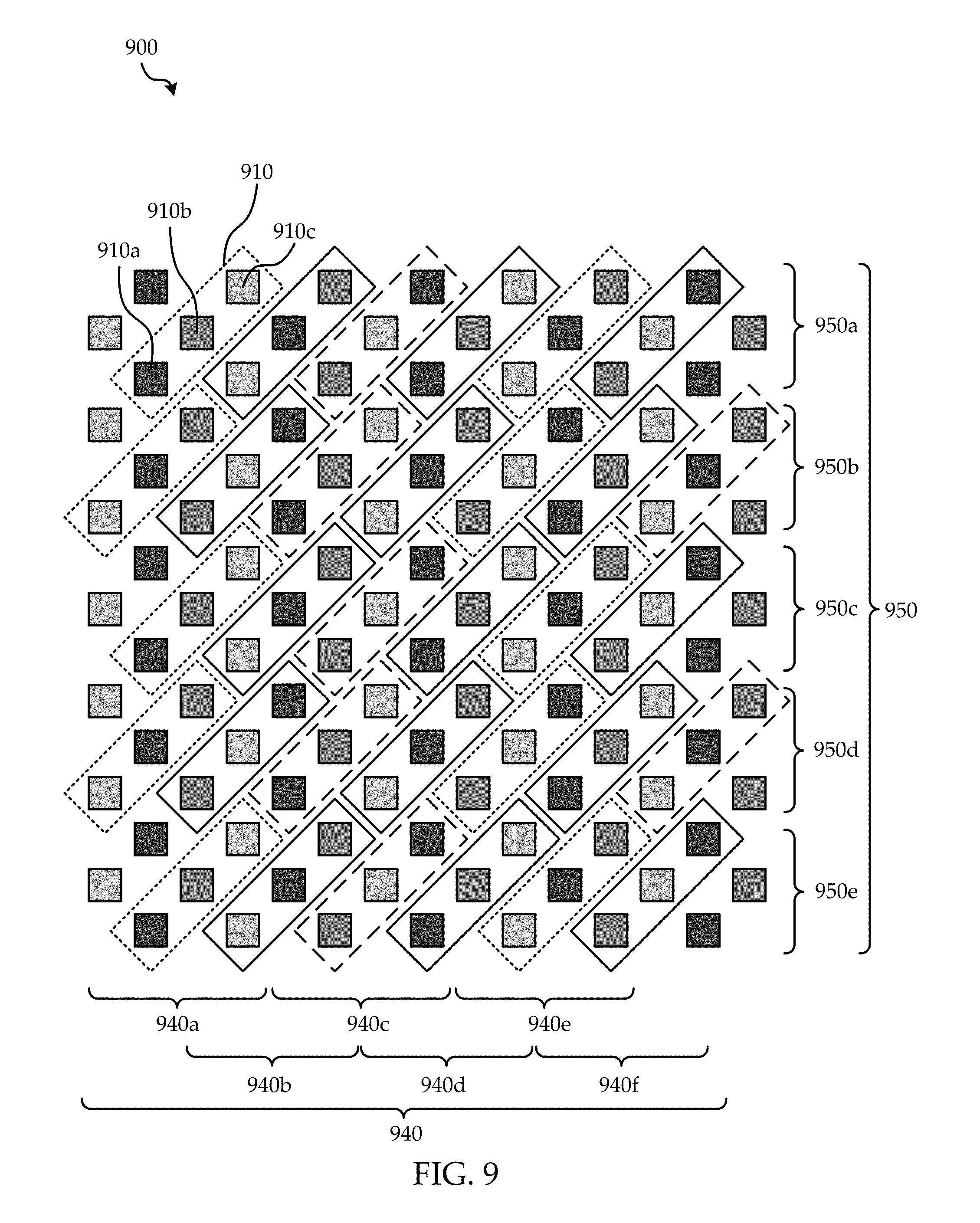
The pixel array architecture 500 of FIG. 5 differs from that of FIG. 2 in how subpixels are arranged into pixels 510. Each pixel is defined from three subpixels 510a, 510b, 510c, in a slanted "I" configuration, each pixel slanting at 45 degrees. Each column 540a, . . . 540f comprises pixels in the "I" configuration arranged in groups of two one atop each other and overlapping only by two subpixels, with a vertical gap of a single subpixel in height between groups, the gap having a subpixel of a pixel of each neighboring column. For example, column 540c (illustrated with dashed lines) includes groups of two pixels, overlapping horizontally (from a vertical perspective) by two subpixels, each group separated by a slanting gap, which in the overlap region includes a subpixel of a pixel of the adjacent column 540b, and a subpixel of a pixel of the adjacent column 540d.
Referring to FIG. 6, a pixel array architecture 600 of a third embodiment will now be discussed.
The pixel array architecture 600 is divided into an array of pixels 610 arranged in individual rows 650a, . . . , 650e, collectively referred to as rows 650 of the display, as well as individual overlapping columns 640a, . . . , 640f, collectively referred to as columns 640 of the display. Each pixel 610 is comprised of a plurality of subpixels 610a, 610b, 610c, each of a different type which is responsible for providing a component, channel, or color of the pixel. In the pixel array architecture 600 of FIG. 6, each pixel is composed of red, green, and blue subpixels, represented in shades of grey in no particular order. It is to be understood that embodiments comprising pixels having subpixels other than red, green, and blue, or a number of subpixels other than three, are contemplated.
In the pixel array architecture 600 each pixel 610 has subpixels 610a, 610b, 610c, in various different orders within a similar configuration. It so happens that subpixels of the same color or type of subpixel are arranged in subpixel columns within the pixel columns 640a even though pixels have various subpixel distributions within them.
Similar to the pixel array architecture of FIG. 2 that of FIG. 6 is based on a diamond shaped subpixel matrix, which is a rectilinear matrix rotated by 45 degrees.
The pixel array architecture 600 of FIG. 6 differs from that of FIG. 2 in how subpixels are arranged into pixels 610. Similar to the embodiment of FIG. 5 each pixel is defined from three subpixels 610a, 610b, 610c, in a slanted "I" configuration, each pixel slanting at positive or negative 45 degrees. Different from the embodiment of FIG. 5 is the inclusion of pixels which slant in different directions, i.e. of opposite slope. Each column 640a, . . . 640f comprises pixels in the "I" configuration arranged one atop each other, alternating in slant form one direction (negative slope) to the other direction (positive slope), and overlapping only by two subpixels, with no vertical gap, but forming a snaking vertical pattern. Moreover, the pixel outline structure of each column is identical to that of its adjacent columns.
Referring to FIG. 7, a pixel array architecture 700 of a fourth embodiment will now be discussed.
The pixel array architecture 700 is divided into an array of pixels 710 arranged in individual overlapping rows 750a, . . . , 750e, collectively referred to as rows 750 of the display, as well as individual overlapping columns 740a, . . . , 740f, collectively referred to as columns 740 of the display. Each pixel 710 is comprised of a plurality of subpixels 710a, 710b, 710c, each of a different type which is responsible for providing a component, channel, or color of the pixel. In the pixel array architecture 700 of FIG. 7, each pixel is composed of red, green, and blue subpixels, represented in shades of grey in no particular order. It is to be understood that embodiments comprising pixels having subpixels other than red, green, and blue, or a number of subpixels other than three, are contemplated.
In the pixel array architecture 700 each pixel 710 has subpixels 710a, 710b, 710c, in various different orders within a similar configuration. It so happens that subpixels of the same color or type of subpixel are arranged in subpixel columns within the pixel columns 740a even though pixels have various subpixel distributions within them.
Similar to the pixel array architecture of FIG. 2 that of FIG. 7 is based on a diamond shaped subpixel matrix, which is a rectilinear matrix rotated by 45 degrees.
The pixel array architecture 700 of FIG. 7 differs from that of FIG. 2 in how subpixels are arranged into pixels 710. Similar to the embodiment of FIG. 7 each pixel is defined from three subpixels 710a, 710b, 710c, in slanted "I" configurations slanting in different directions, each pixel slanting at positive or negative 45 degrees. Each column 740a, . . . 740f comprises pixels in the "I" configuration arranged one atop each other, alternating in slant form one direction (negative 45 degree slope) to the other direction (positive 45 degree slope), and overlapping only by two subpixels, with no vertical gap, but forming a snaking vertical pattern. In this embodiment, as opposed to that of FIG. 6, the pixel outline structure of each column is not identical to that of its adjacent columns. In the snaking pattern of one column, an upper pixel sits atop the pixel below it on the longest side of the pixel below, while in an adjacent column, the upper pixel sits atop the pixel below it on the shortest side of the pixel below. This results in a slightly different pattern having overlapping rows 750a, . . . , 750e.
Referring to FIG. 8, a pixel array architecture 800 of a fifth embodiment will now be discussed.
The pixel array architecture 800 is divided into an array of pixels 810 arranged in individual rows 850a, . . . , 850c, collectively referred to as rows 850 of the display, as well as individual overlapping columns 840a, . . . , 840g, collectively referred to as columns 840 of the display. Each pixel 810 is comprised of a plurality of subpixels 810a, 810b, 810c, each of a different type which is responsible for providing a component, channel, or color of the pixel. In the pixel array architecture 800 of FIG. 8, each pixel is composed of red, green, and blue subpixels, represented in shades of grey in no particular order. It is to be understood that embodiments comprising pixels having subpixels other than red, green, and blue, or a number of subpixels other than three, are contemplated.
In the pixel array architecture 800 each pixel 810 has subpixels 810a, 810b, 810c, in various different orders within a similar configuration. It so happens that subpixels of the same color or type of subpixel are arranged in subpixel columns within the pixel columns 840a even though pixels have various subpixel distributions within them.
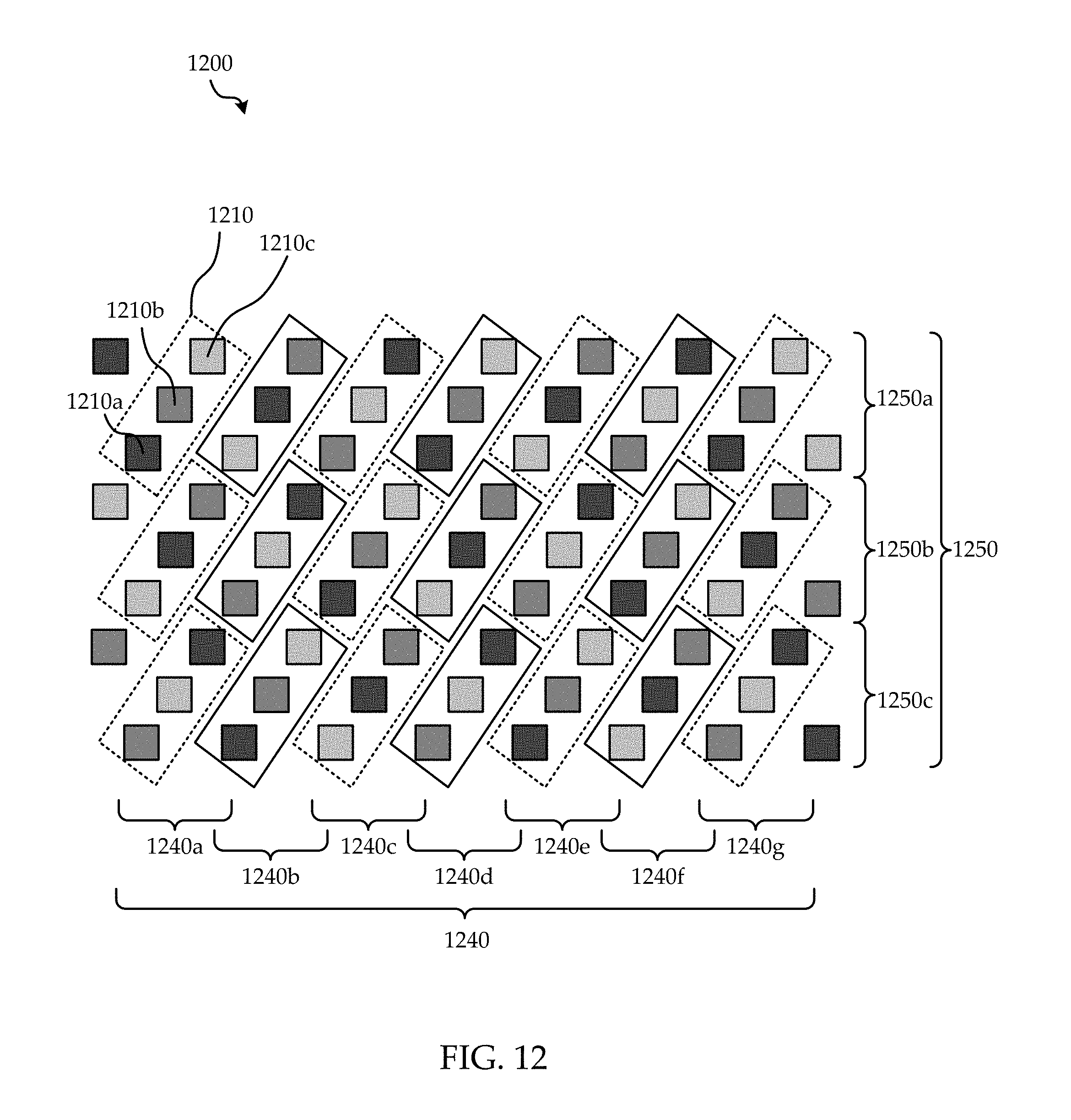
Similar to the pixel array architecture of FIG. 2 that of FIG. 5 is based on a diamond shaped subpixel matrix, which is a rectilinear matrix rotated by 45 degrees, but with a further skew or parallelogram transformation to bring the defined pixels into columns in the vertical direction.
The pixel array architecture 800 of FIG. 8 is similar to that of FIG. 5 in that each pixel is defined from three subpixels 810a, 810b, 810c, in a slanted "I" configuration. It differs from that of FIG. 5 in that the pixels, by virtue of the skewed array, can be arranged atop one another in slightly overlapping vertical columns 840a, . . . , 840g. In particular every subpixel is vertically aligned with subpixels in every third subpixel row, i.e. each subpixel of a pixel is aligned with the same positioned subpixel in the pixel below it.
FIG. 9, FIG. 10, FIG. 11, and FIG. 12, illustrate variations of embodiments respectively depicted in FIG. 5, FIG. 6, FIG. 7, and FIG. 8. Each of the pixel array architectures 900, 1000, 1100, and 1200 is substantially equivalent respectively to pixel array architecture 500, 600, 700, and 800 differing only by use of square subpixels whose sides are parallel to the vertical and horizontal directions of the display rather than rotated at 45 degrees as is the case for the subpixels of each of architectures 500, 600, 700, and 800 of respectively FIG. 5, FIG. 6, FIG. 7, and FIG. 8.
Referring to FIG. 13, a pixel array architecture 1300 of a sixth embodiment will now be discussed.
The pixel array architecture 1300 is divided into an array of pixels 1310, 1320 arranged in individual overlapping rows 1350a, . . . , 1350f, collectively referred to as rows 1350 of the display, as well as individual overlapping columns 1340a, . . . , 1340f, collectively referred to as columns 1340 of the display. Each pixel 1310 is comprised of a plurality of subpixels 1310a, 1310b, which it does not share with other pixels and a plurality of subpixels 1305, 1315 which it does share with other pixels. Within each pixel each subpixel is of a different type which is responsible for providing a component, channel, or color of the pixel.
In the pixel array architecture 1300 of FIG. 13, each pixel is composed of a green 1320a and a white 1310b unshared subpixel, as well as a shared red 1305 and a shared blue 1315 subpixel, each represented in a corresponding shade of grey. Because red and blue offer more color information on a typical display, they have been chosen as the shared pixels to minimize loss of information. It is to be understood that embodiments comprising pixels having subpixels other than red, green, blue, and white, or a number of subpixels other than four, are contemplated. It is also to be understood that subpixels of colors other than red or blue may be shared between pixels, that green and white subpixels may be shared, and that subpixels other than white and green may be unshared, including red and blue subpixels.
In the pixel array architecture 1300 each pixel 1310 has a green subpixel 1310a as its uppermost subpixel, a white subpixel 1310b as it lowermost subpixel and one of a red or a blue subpixel as its leftmost subpixel and the other of a red or blue subpixel as its rightmost subpixel. For example, in each row 1350a, . . . , 1350f, pixels of alternating columns have alternating left-right configurations of red and blue subpixels.
The green and white subpixels of the pixel array architecture 1300 each form subpixel rows within each row 1350a, . . . , 1350f, while the red and blue subpixels forms a subpixel row of alternating red and blue subpixels within each row 1350a, . . . , 1350f.
The pixel array architecture of FIG. 13 is based on a diamond shaped subpixel matrix, which is a rectilinear matrix rotated by 45 degrees. Each pixel is defined from four subpixels 1310a, 1310b, 1305, 1315, in a diamond configuration. Each column 1340a, . . . 1340f comprises pixels in the diamond configuration arranged one atop of the other in a snaking pattern, overlapping horizontally by two subpixels, from a vertical perspective. Adjacent columns 1340 snake in the same direction at each row.
Although pixels in the various embodiment have been depicted with particular orientations, it should be understood that equivalent orientations of each embodiment obtained by a reflection in the horizontal or vertical axis or a rotation of a multiple of 90 degrees is contemplated. For clarity an embodiment having an arrangement of "v" and an upside down "v" shaped pixels is equivalent to an embodiment with right opening "v" and left opening "v" shaped pixels.
While the present disclosure is susceptible to various modifications and alternative forms, specific embodiments or implementations have been shown by way of example in the drawings and will be described in detail herein. It should be understood, however, that the disclosure is not intended to be limited to the particular forms disclosed. Rather, the disclosure is to cover all modifications, equivalents, and alternatives falling within the spirit and scope of an invention as defined by the appended claims.
While particular implementations and applications of the present disclosure have been illustrated and described, it is to be understood that the present disclosure is not limited to the precise construction and compositions disclosed herein and that various modifications, changes, and variations can be apparent from the foregoing descriptions without departing from the spirit and scope of an invention as defined in the appended claims.
* * * * *
D00000
D00001
D00002
D00003
D00004
D00005
D00006
D00007
D00008
D00009
D00010
D00011
D00012
D00013

XML
uspto.report is an independent third-party trademark research tool that is not affiliated, endorsed, or sponsored by the United States Patent and Trademark Office (USPTO) or any other governmental organization. The information provided by uspto.report is based on publicly available data at the time of writing and is intended for informational purposes only.
While we strive to provide accurate and up-to-date information, we do not guarantee the accuracy, completeness, reliability, or suitability of the information displayed on this site. The use of this site is at your own risk. Any reliance you place on such information is therefore strictly at your own risk.
All official trademark data, including owner information, should be verified by visiting the official USPTO website at www.uspto.gov. This site is not intended to replace professional legal advice and should not be used as a substitute for consulting with a legal professional who is knowledgeable about trademark law.