Display system
Nathan , et al. May 4, 2
U.S. patent number 10,997,901 [Application Number 14/630,906] was granted by the patent office on 2021-05-04 for display system. This patent grant is currently assigned to Ignis Innovation Inc.. The grantee listed for this patent is Ignis Innovation Inc.. Invention is credited to Gholamreza Chaji, Joseph Marcel Dionne, Arokia Nathan.


| United States Patent | 10,997,901 |
| Nathan , et al. | May 4, 2021 |
Display system
Abstract
A method of recovering a display having a plurality of pixels, each having a light emitting device and a driving transistor for driving the light emitting device. The driving transistor and the light emitting device are coupled in series between a first power supply and a second power supply. The method illuminates the semiconductor device while negatively biasing the pixel circuit with a recovery voltage different from an image programming voltage. The illuminating may follow a first cycle implementing an image display operation that includes programming the pixel circuit for a valid image and driving the pixel circuit to emit light according to the programming.
| Inventors: | Nathan; Arokia (Cambridge, GB), Chaji; Gholamreza (Waterloo, CA), Dionne; Joseph Marcel (Waterloo, CA) | ||||||||||
|---|---|---|---|---|---|---|---|---|---|---|---|
| Applicant: |
|
||||||||||
| Assignee: | Ignis Innovation Inc.
(Waterloo, CA) |
||||||||||
| Family ID: | 1000005531214 | ||||||||||
| Appl. No.: | 14/630,906 | ||||||||||
| Filed: | February 25, 2015 |
Prior Publication Data
| Document Identifier | Publication Date | |
|---|---|---|
| US 20150248860 A1 | Sep 3, 2015 | |
Related U.S. Patent Documents
| Application Number | Filing Date | Patent Number | Issue Date | ||
|---|---|---|---|---|---|
| 61946427 | Feb 28, 2014 | ||||
| Current U.S. Class: | 1/1 |
| Current CPC Class: | G09G 3/3233 (20130101); G09G 3/3208 (20130101); G09G 3/3258 (20130101); G09G 2310/0251 (20130101); G09G 2330/027 (20130101); G09G 2300/0819 (20130101); G09G 2310/0254 (20130101); G09G 2300/0852 (20130101); G09G 2320/048 (20130101); G09G 2310/0256 (20130101); G09G 2320/045 (20130101); G09G 2300/0861 (20130101); G09G 3/3291 (20130101) |
| Current International Class: | G09G 3/32 (20160101); G09G 3/3208 (20160101); G09G 3/3233 (20160101); G09G 3/3258 (20160101); G09G 3/3291 (20160101) |
| Field of Search: | ;345/208,173,211 |
References Cited [Referenced By]
U.S. Patent Documents
| 4354162 | October 1982 | Wright |
| 4758831 | July 1988 | Kasahara et al. |
| 4963860 | October 1990 | Stewart |
| 4975691 | December 1990 | Lee |
| 4996523 | February 1991 | Bell et al. |
| 5051739 | September 1991 | Hayashida et al. |
| 5222082 | June 1993 | Plus |
| 5266515 | November 1993 | Robb et al. |
| 5498880 | March 1996 | Lee et al. |
| 5589847 | December 1996 | Lewis |
| 5619033 | April 1997 | Weisfield |
| 5648276 | July 1997 | Hara et al. |
| 5670973 | September 1997 | Bassetti et al. |
| 5684365 | November 1997 | Tang et al. |
| 5686935 | November 1997 | Weisbrod |
| 5712653 | January 1998 | Katoh et al. |
| 5714968 | February 1998 | Ikeda |
| 5747928 | May 1998 | Shanks et al. |
| 5748160 | May 1998 | Shieh et al. |
| 5784042 | July 1998 | Ono et al. |
| 5790234 | August 1998 | Matsuyama |
| 5815303 | September 1998 | Berlin |
| 5870071 | February 1999 | Kawahata |
| 5874803 | February 1999 | Garbuzov et al. |
| 5880582 | March 1999 | Sawada |
| 5903248 | May 1999 | Irwin |
| 5917280 | June 1999 | Burrows et al. |
| 5923794 | July 1999 | McGrath et al. |
| 5952789 | September 1999 | Stewart et al. |
| 5990629 | November 1999 | Yamada et al. |
| 6023259 | February 2000 | Howard et al. |
| 6069365 | May 2000 | Chow et al. |
| 6081131 | June 2000 | Ishii |
| 6091203 | July 2000 | Kawashima et al. |
| 6097360 | August 2000 | Holloman |
| 6144222 | November 2000 | Ho |
| 6157583 | December 2000 | Starnes et al. |
| 6166489 | December 2000 | Thompson et al. |
| 6177915 | January 2001 | Beeteson et al. |
| 6225846 | May 2001 | Wada et al. |
| 6229508 | May 2001 | Kane |
| 6232939 | May 2001 | Saito et al. |
| 6246180 | June 2001 | Nishigaki |
| 6252248 | June 2001 | Sano et al. |
| 6259424 | July 2001 | Kurogane |
| 6274887 | August 2001 | Yamazaki et al. |
| 6288696 | September 2001 | Holloman |
| 6300928 | October 2001 | Kim |
| 6303963 | October 2001 | Ohtani et al. |
| 6306694 | October 2001 | Yamazaki et al. |
| 6307322 | October 2001 | Dawson et al. |
| 6316786 | November 2001 | Mueller et al. |
| 6320325 | November 2001 | Cok et al. |
| 6323631 | November 2001 | Juang |
| 6323832 | November 2001 | Nishizawa et al. |
| 6345085 | February 2002 | Yeo et al. |
| 6348835 | February 2002 | Sato et al. |
| 6365917 | April 2002 | Yamazaki |
| 6373453 | April 2002 | Yudasaka |
| 6384427 | May 2002 | Yamazaki et al. |
| 6392617 | May 2002 | Gleason |
| 6399988 | June 2002 | Yamazaki |
| 6414661 | July 2002 | Shen et al. |
| 6420758 | July 2002 | Nakajima |
| 6420834 | July 2002 | Yamazaki et al. |
| 6420988 | July 2002 | Azami et al. |
| 6433488 | August 2002 | Bu |
| 6445376 | September 2002 | Parrish |
| 6468638 | October 2002 | Jacobsen et al. |
| 6489952 | December 2002 | Tanaka et al. |
| 6501098 | December 2002 | Yamazaki |
| 6501466 | December 2002 | Yamagashi et al. |
| 6512271 | January 2003 | Yamazaki et al. |
| 6518594 | February 2003 | Nakajima et al. |
| 6524895 | February 2003 | Yamazaki et al. |
| 6531713 | March 2003 | Yamazaki |
| 6559594 | May 2003 | Fukunaga et al. |
| 6573195 | June 2003 | Yamazaki et al. |
| 6573584 | June 2003 | Nagakari et al. |
| 6576926 | June 2003 | Yamazaki et al. |
| 6580408 | June 2003 | Bae et al. |
| 6580657 | June 2003 | Sanford et al. |
| 6583775 | June 2003 | Sekiya et al. |
| 6583776 | June 2003 | Yamazaki et al. |
| 6587086 | July 2003 | Koyama |
| 6593691 | July 2003 | Nishi et al. |
| 6594606 | July 2003 | Everitt |
| 6597203 | July 2003 | Forbes |
| 6611108 | August 2003 | Kimura |
| 6617644 | September 2003 | Yamazaki et al. |
| 6618030 | September 2003 | Kane et al. |
| 6641933 | November 2003 | Yamazaki et al. |
| 6661180 | December 2003 | Koyama |
| 6661397 | December 2003 | Mikami et al. |
| 6670637 | December 2003 | Yamazaki et al. |
| 6677713 | January 2004 | Sung |
| 6680577 | January 2004 | Inukai et al. |
| 6687266 | February 2004 | Ma et al. |
| 6690344 | February 2004 | Takeuchi et al. |
| 6693388 | February 2004 | Oomura |
| 6693610 | February 2004 | Shannon et al. |
| 6697057 | February 2004 | Koyama et al. |
| 6720942 | April 2004 | Lee et al. |
| 6734636 | May 2004 | Sanford et al. |
| 6738034 | May 2004 | Kaneko et al. |
| 6738035 | May 2004 | Fan |
| 6771028 | August 2004 | Winters |
| 6777712 | August 2004 | Sanford et al. |
| 6780687 | August 2004 | Nakajima et al. |
| 6806638 | October 2004 | Lih et al. |
| 6806857 | October 2004 | Sempel et al. |
| 6809706 | October 2004 | Shimoda |
| 6859193 | February 2005 | Yumoto |
| 6861670 | March 2005 | Ohtani et al. |
| 6873117 | March 2005 | Ishizuka |
| 6873320 | March 2005 | Nakamura |
| 6878968 | April 2005 | Ohnuma |
| 6909114 | June 2005 | Yamazaki |
| 6909419 | June 2005 | Zavracky et al. |
| 6919871 | July 2005 | Kwon |
| 6937215 | August 2005 | Lo |
| 6940214 | September 2005 | Komiya et al. |
| 6943500 | September 2005 | LeChevalier |
| 6954194 | October 2005 | Matsumoto et al. |
| 6956547 | October 2005 | Bae et al. |
| 6995510 | February 2006 | Murakami et al. |
| 6995519 | February 2006 | Arnold et al. |
| 7022556 | April 2006 | Adachi |
| 7023408 | April 2006 | Chen et al. |
| 7027015 | April 2006 | Booth, Jr. et al. |
| 7034793 | April 2006 | Sekiya et al. |
| 7088051 | August 2006 | Cok |
| 7106285 | September 2006 | Naugler |
| 7116058 | October 2006 | Lo et al. |
| 7129914 | October 2006 | Knapp et al. |
| 7129917 | October 2006 | Yamazaki et al. |
| 7141821 | November 2006 | Yamazaki et al. |
| 7161566 | January 2007 | Cok et al. |
| 7193589 | March 2007 | Yoshida et al. |
| 7199516 | April 2007 | Seo et al. |
| 7220997 | May 2007 | Nakata |
| 7235810 | June 2007 | Yamazaki et al. |
| 7245277 | July 2007 | Ishizuka |
| 7248236 | July 2007 | Nathan et al. |
| 7264979 | September 2007 | Yamagata et al. |
| 7274345 | September 2007 | Imamura et al. |
| 7274363 | September 2007 | Ishizuka et al. |
| 7279711 | October 2007 | Yamazaki et al. |
| 7304621 | December 2007 | Oomori et al. |
| 7310092 | December 2007 | Imamura |
| 7315295 | January 2008 | Kimura |
| 7317429 | January 2008 | Shirasaki et al. |
| 7319465 | January 2008 | Mikami et al. |
| 7321348 | January 2008 | Cok et al. |
| 7339636 | March 2008 | Voloschenko et al. |
| 7355574 | April 2008 | Leon et al. |
| 7358941 | April 2008 | Ono et al. |
| 7402467 | July 2008 | Kadono et al. |
| 7414600 | August 2008 | Nathan et al. |
| 7432885 | October 2008 | Asano et al. |
| 7474285 | January 2009 | Kimura |
| 7485478 | February 2009 | Yamagata et al. |
| 7502000 | March 2009 | Yuki et al. |
| 7535449 | May 2009 | Miyazawa |
| 7554512 | June 2009 | Steer |
| 7569849 | August 2009 | Nathan et al. |
| 7619594 | November 2009 | Hu |
| 7619597 | November 2009 | Nathan et al. |
| 7697052 | April 2010 | Yamazaki et al. |
| 7825419 | November 2010 | Yamagata et al. |
| 7859492 | December 2010 | Kohno |
| 7868859 | January 2011 | Tomida et al. |
| 7876294 | January 2011 | Sasaki et al. |
| 7948170 | May 2011 | Striakhilev et al. |
| 7969390 | June 2011 | Yoshida |
| 7995010 | August 2011 | Yamazaki et al. |
| 8044893 | October 2011 | Nathan et al. |
| 8115707 | February 2012 | Nathan et al. |
| 8299984 | October 2012 | Nathan |
| 8378362 | February 2013 | Heo et al. |
| 8493295 | July 2013 | Yamazaki et al. |
| 8497525 | July 2013 | Yamagata et al. |
| 2001/0002703 | June 2001 | Koyama |
| 2001/0004190 | June 2001 | Nishi et al. |
| 2001/0013806 | August 2001 | Notani |
| 2001/0015653 | August 2001 | De Jong et al. |
| 2001/0020926 | September 2001 | Kujik |
| 2001/0026127 | October 2001 | Yoneda et al. |
| 2001/0026179 | October 2001 | Saeki |
| 2001/0026257 | October 2001 | Kimura |
| 2001/0030323 | October 2001 | Ikeda |
| 2001/0033199 | October 2001 | Aoki |
| 2001/0038098 | November 2001 | Yamazaki et al. |
| 2001/0043173 | November 2001 | Troutman |
| 2001/0045929 | November 2001 | Prache et al. |
| 2001/0052606 | December 2001 | Sempel et al. |
| 2001/0052898 | December 2001 | Osame et al. |
| 2002/0000576 | January 2002 | Inukai |
| 2002/0011796 | January 2002 | Koyama |
| 2002/0011799 | January 2002 | Kimura |
| 2002/0011981 | January 2002 | Kujik |
| 2002/0015031 | February 2002 | Fujita et al. |
| 2002/0015032 | February 2002 | Koyama et al. |
| 2002/0030528 | March 2002 | Matsumoto et al. |
| 2002/0030647 | March 2002 | Hack et al. |
| 2002/0036463 | March 2002 | Yoneda et al. |
| 2002/0047852 | April 2002 | Inukai et al. |
| 2002/0048829 | April 2002 | Yamazaki et al. |
| 2002/0050795 | May 2002 | Imura |
| 2002/0053401 | May 2002 | Ishikawa et al. |
| 2002/0070909 | June 2002 | Asano et al. |
| 2002/0080108 | June 2002 | Wang |
| 2002/0084463 | July 2002 | Sanford et al. |
| 2002/0101172 | August 2002 | Bu |
| 2002/0101433 | August 2002 | McKnight |
| 2002/0113248 | August 2002 | Yamagata et al. |
| 2002/0122308 | September 2002 | Ikeda |
| 2002/0130686 | September 2002 | Forbes |
| 2002/0154084 | October 2002 | Tanaka et al. |
| 2002/0158823 | October 2002 | Zavracky et al. |
| 2002/0163314 | November 2002 | Yamazaki et al. |
| 2002/0167471 | November 2002 | Everitt |
| 2002/0180369 | December 2002 | Koyama |
| 2002/0180721 | December 2002 | Kimura et al. |
| 2002/0186214 | December 2002 | Siwinski |
| 2002/0190332 | December 2002 | Lee et al. |
| 2002/0190924 | December 2002 | Asano et al. |
| 2002/0190971 | December 2002 | Nakamura et al. |
| 2002/0195967 | December 2002 | Kim et al. |
| 2002/0195968 | December 2002 | Sanford et al. |
| 2003/0020413 | January 2003 | Oomura |
| 2003/0030603 | February 2003 | Shimoda |
| 2003/0062524 | April 2003 | Kimura |
| 2003/0063081 | April 2003 | Kimura et al. |
| 2003/0071804 | April 2003 | Yamazaki et al. |
| 2003/0076048 | April 2003 | Rutherford |
| 2003/0090445 | May 2003 | Chen et al. |
| 2003/0090447 | May 2003 | Kimura |
| 2003/0090481 | May 2003 | Kimura |
| 2003/0095087 | May 2003 | Libsch |
| 2003/0107560 | June 2003 | Yumoto et al. |
| 2003/0111966 | June 2003 | Mikami et al. |
| 2003/0122745 | July 2003 | Miyazawa |
| 2003/0140958 | July 2003 | Yang et al. |
| 2003/0151569 | August 2003 | Lee et al. |
| 2003/0169219 | September 2003 | LeChevalier |
| 2003/0174152 | September 2003 | Noguchi |
| 2003/0179626 | September 2003 | Sanford et al. |
| 2003/0197663 | October 2003 | Lee et al. |
| 2003/0206060 | November 2003 | Suzuki |
| 2003/0230980 | December 2003 | Forrest et al. |
| 2004/0027063 | February 2004 | Nishikawa |
| 2004/0056604 | March 2004 | Shih et al. |
| 2004/0066357 | April 2004 | Kawasaki |
| 2004/0070557 | April 2004 | Asano et al. |
| 2004/0080262 | April 2004 | Park et al. |
| 2004/0080470 | April 2004 | Yamazaki et al. |
| 2004/0090400 | May 2004 | Yoo |
| 2004/0108518 | June 2004 | Jo |
| 2004/0113903 | June 2004 | Mikami et al. |
| 2004/0129933 | July 2004 | Nathan et al. |
| 2004/0130516 | July 2004 | Nathan et al. |
| 2004/0135749 | July 2004 | Kondakov et al. |
| 2004/0145547 | July 2004 | Oh |
| 2004/0150592 | August 2004 | Mizukoshi et al. |
| 2004/0150594 | August 2004 | Koyama et al. |
| 2004/0150595 | August 2004 | Kasai |
| 2004/0155841 | August 2004 | Kasai |
| 2004/0174347 | September 2004 | Sun et al. |
| 2004/0174349 | September 2004 | Libsch |
| 2004/0179005 | September 2004 | Jo |
| 2004/0183759 | September 2004 | Stevenson et al. |
| 2004/0189627 | September 2004 | Shirasaki et al. |
| 2004/0196275 | October 2004 | Hattori |
| 2004/0201554 | October 2004 | Satoh |
| 2004/0207615 | October 2004 | Yumoto |
| 2004/0233125 | November 2004 | Tanghe et al. |
| 2004/0239596 | December 2004 | Ono et al. |
| 2004/0252089 | December 2004 | Ono et al. |
| 2004/0257355 | December 2004 | Naugler |
| 2004/0263437 | December 2004 | Hattori |
| 2005/0007357 | January 2005 | Yamashita et al. |
| 2005/0030267 | February 2005 | Tanghe et al. |
| 2005/0035709 | February 2005 | Furuie et al. |
| 2005/0057459 | March 2005 | Miyazawa |
| 2005/0067970 | March 2005 | Libsch et al. |
| 2005/0067971 | March 2005 | Kane |
| 2005/0068270 | March 2005 | Awakura |
| 2005/0088085 | April 2005 | Nishikawa et al. |
| 2005/0088103 | April 2005 | Kageyama et al. |
| 2005/0110420 | May 2005 | Arnold et al. |
| 2005/0117096 | June 2005 | Voloschenko et al. |
| 2005/0140598 | June 2005 | Kim et al. |
| 2005/0140610 | June 2005 | Smith et al. |
| 2005/0145891 | July 2005 | Abe |
| 2005/0156831 | July 2005 | Yamazaki et al. |
| 2005/0168416 | August 2005 | Hashimoto et al. |
| 2005/0206590 | September 2005 | Sasaki et al. |
| 2005/0225686 | October 2005 | Brummack et al. |
| 2005/0260777 | November 2005 | Brabec et al. |
| 2005/0269959 | December 2005 | Uchino et al. |
| 2005/0269960 | December 2005 | Ono et al. |
| 2005/0285822 | December 2005 | Reddy et al. |
| 2005/0285825 | December 2005 | Eom et al. |
| 2006/0007072 | January 2006 | Choi et al. |
| 2006/0012310 | January 2006 | Chen et al. |
| 2006/0027807 | February 2006 | Nathan et al. |
| 2006/0030084 | February 2006 | Young |
| 2006/0038758 | February 2006 | Routley et al. |
| 2006/0044227 | March 2006 | Hadcock |
| 2006/0066527 | March 2006 | Chou |
| 2006/0092185 | May 2006 | Jo et al. |
| 2006/0097965 | May 2006 | Deane |
| 2006/0187154 | August 2006 | Tsuchida |
| 2006/0232522 | October 2006 | Roy et al. |
| 2006/0261841 | November 2006 | Fish |
| 2006/0264143 | November 2006 | Lee et al. |
| 2006/0273997 | December 2006 | Nathan |
| 2006/0284801 | December 2006 | Yoon et al. |
| 2007/0001937 | January 2007 | Park et al. |
| 2007/0001939 | January 2007 | Hashimoto et al. |
| 2007/0008268 | January 2007 | Park et al. |
| 2007/0008297 | January 2007 | Bassetti |
| 2007/0046195 | March 2007 | Chin et al. |
| 2007/0069998 | March 2007 | Naugler et al. |
| 2007/0080905 | April 2007 | Takahara |
| 2007/0080906 | April 2007 | Tanabe |
| 2007/0080908 | April 2007 | Nathan et al. |
| 2007/0080918 | April 2007 | Kawachi et al. |
| 2007/0103419 | May 2007 | Uchino et al. |
| 2007/0120785 | May 2007 | Kimura |
| 2007/0182671 | August 2007 | Nathan et al. |
| 2007/0273294 | November 2007 | Nagayama |
| 2007/0285359 | December 2007 | Ono |
| 2007/0296672 | December 2007 | Kim et al. |
| 2008/0042948 | February 2008 | Yamashita |
| 2008/0055209 | March 2008 | Cok |
| 2008/0074413 | March 2008 | Ogura |
| 2008/0088549 | April 2008 | Nathan et al. |
| 2008/0122803 | May 2008 | Izadi et al. |
| 2008/0230118 | September 2008 | Nakatani et al. |
| 2009/0032807 | February 2009 | Shinohara et al. |
| 2009/0051283 | February 2009 | Cok et al. |
| 2009/0096722 | April 2009 | Moriya |
| 2009/0160743 | June 2009 | Tomida et al. |
| 2009/0162961 | June 2009 | Deane |
| 2009/0167644 | July 2009 | White |
| 2009/0174628 | July 2009 | Wang et al. |
| 2009/0184898 | July 2009 | Yamashita |
| 2009/0213046 | August 2009 | Nam |
| 2009/0262101 | October 2009 | Nathan |
| 2009/0284451 | November 2009 | Yamamoto |
| 2010/0013746 | January 2010 | Seto |
| 2010/0052524 | March 2010 | Kinoshita |
| 2010/0078230 | April 2010 | Rosenblatt et al. |
| 2010/0079711 | April 2010 | Tanaka |
| 2010/0097335 | April 2010 | Jung |
| 2010/0133994 | June 2010 | Song et al. |
| 2010/0134456 | June 2010 | Oyamada |
| 2010/0156279 | June 2010 | Tamura et al. |
| 2010/0225634 | September 2010 | Levey |
| 2010/0237374 | September 2010 | Chu et al. |
| 2010/0328294 | December 2010 | Sasaki et al. |
| 2011/0069059 | March 2011 | Lee |
| 2011/0090210 | April 2011 | Sasaki et al. |
| 2011/0133636 | June 2011 | Matsuo et al. |
| 2011/0134157 | June 2011 | Chaji |
| 2011/0180825 | July 2011 | Lee et al. |
| 2012/0212468 | August 2012 | Govil |
| 2013/0009930 | January 2013 | Cho |
| 2013/0032831 | February 2013 | Chaji et al. |
| 2013/0113785 | May 2013 | Sumi |
| 1294034 | Jan 1992 | CA | |||
| 2109951 | Nov 1992 | CA | |||
| 2 249 592 | Jul 1998 | CA | |||
| 2 368 386 | Sep 1999 | CA | |||
| 2 242 720 | Jan 2000 | CA | |||
| 2 354 018 | Jun 2000 | CA | |||
| 2 436 451 | Aug 2002 | CA | |||
| 2 438 577 | Aug 2002 | CA | |||
| 2 483 645 | Dec 2003 | CA | |||
| 2 463 653 | Jan 2004 | CA | |||
| 2498136 | Mar 2004 | CA | |||
| 2522396 | Nov 2004 | CA | |||
| 2443206 | Mar 2005 | CA | |||
| 2472671 | Dec 2005 | CA | |||
| 2567076 | Jan 2006 | CA | |||
| 2526782 | Apr 2006 | CA | |||
| 1381032 | Nov 2002 | CN | |||
| 1448908 | Oct 2003 | CN | |||
| 20 2006 005427 | Jun 2006 | DE | |||
| 0 940 796 | Sep 1999 | EP | |||
| 1 028 471 | Aug 2000 | EP | |||
| 1 103 947 | May 2001 | EP | |||
| 1 130 565 | Sep 2001 | EP | |||
| 1 184 833 | Mar 2002 | EP | |||
| 1 194 013 | Apr 2002 | EP | |||
| 1 310 939 | May 2003 | EP | |||
| 1 335 430 | Aug 2003 | EP | |||
| 1 372 136 | Dec 2003 | EP | |||
| 1 381 019 | Jan 2004 | EP | |||
| 1 418 566 | May 2004 | EP | |||
| 1 429 312 | Jun 2004 | EP | |||
| 1 439 520 | Jul 2004 | EP | |||
| 1 465 143 | Oct 2004 | EP | |||
| 1 467 408 | Oct 2004 | EP | |||
| 1 517 290 | Mar 2005 | EP | |||
| 1 521 203 | Apr 2005 | EP | |||
| 2317499 | May 2011 | EP | |||
| 2 205 431 | Dec 1988 | GB | |||
| 09 090405 | Apr 1997 | JP | |||
| 10-153759 | Jun 1998 | JP | |||
| 10-254410 | Sep 1998 | JP | |||
| 11 231805 | Aug 1999 | JP | |||
| 11-282419 | Oct 1999 | JP | |||
| 2000/056847 | Feb 2000 | JP | |||
| 2000-077192 | Mar 2000 | JP | |||
| 2000-089198 | Mar 2000 | JP | |||
| 2000-352941 | Dec 2000 | JP | |||
| 2002-91376 | Mar 2002 | JP | |||
| 2002-268576 | Sep 2002 | JP | |||
| 2002-278513 | Sep 2002 | JP | |||
| 2002-333862 | Nov 2002 | JP | |||
| 2003-022035 | Jan 2003 | JP | |||
| 2003-076331 | Mar 2003 | JP | |||
| 2003-150082 | May 2003 | JP | |||
| 2003-177709 | Jun 2003 | JP | |||
| 2003-271095 | Sep 2003 | JP | |||
| 2003-308046 | Oct 2003 | JP | |||
| 2005-057217 | Mar 2005 | JP | |||
| 2006065148 | Mar 2006 | JP | |||
| 2009282158 | Dec 2009 | JP | |||
| 485337 | May 2002 | TW | |||
| 502233 | Sep 2002 | TW | |||
| 538650 | Jun 2003 | TW | |||
| 569173 | Jan 2004 | TW | |||
| WO 94/25954 | Nov 1994 | WO | |||
| WO 9948079 | Sep 1999 | WO | |||
| WO 01/27910 | Apr 2001 | WO | |||
| WO 02/067327 | Aug 2002 | WO | |||
| WO 03/034389 | Apr 2003 | WO | |||
| WO 03/063124 | Jul 2003 | WO | |||
| WO 03/077231 | Sep 2003 | WO | |||
| WO 03/105117 | Dec 2003 | WO | |||
| WO 2004/003877 | Jan 2004 | WO | |||
| WO 2004/034364 | Apr 2004 | WO | |||
| WO 2005/022498 | Mar 2005 | WO | |||
| WO 2005/029455 | Mar 2005 | WO | |||
| WO 2005/055185 | Jun 2005 | WO | |||
| WO 2006/053424 | May 2006 | WO | |||
| WO 2006/063448 | Jun 2006 | WO | |||
| WO 2006/137337 | Dec 2006 | WO | |||
| WO 2007/003877 | Jan 2007 | WO | |||
| WO 2007/079572 | Jul 2007 | WO | |||
| WO 2010/023270 | Mar 2010 | WO | |||
| WO 2011052472 | May 2011 | WO | |||
Other References
|
Ahnood et al.: "Effect of threshold voltage instability on field effect mobility in thin film transistors deduced from constant current measurements"; dated Aug. 2009 (3 pages). cited by applicant . Alexander et al.: "Pixel circuits and drive schemes for glass and elastic AMOLED displays"; dated Jul. 2005 (9 pages). cited by applicant . Alexander et al.: "Unique Electrical Measurement Technology for Compensation, Inspection, and Process Diagnostics of AMOLED HDTV"; dated May 2010 (4 pages). cited by applicant . Ashtiani et al.: "AMOLED Pixel Circuit With Electronic Compensation of Luminance Degradation"; dated Mar. 2007 (4 pages). cited by applicant . Chaji et al.: "A Current-Mode Comparator for Digital Calibration of Amorphous Silicon AMOLED Displays"; dated Jul. 2008 (5 pages). cited by applicant . Chaji et al.: "A fast settling current driver based on the CCII for AMOLED displays"; dated Dec. 2009 (6 pages). cited by applicant . Chaji et al.: "A Low-Cost Stable Amorphous Silicon AMOLED Display with Full V.about.T- and V.about.O.about.L.about.E.about.D Shift Compensation"; dated May 2007 (4 pages). cited by applicant . Chaji et al.: "A low-power driving scheme for a-Si:H active-matrix organic light-emitting diode displays"; dated Jun. 2005 (4 pages). cited by applicant . Chaji et al.: "A low-power high-performance digital circuit for deep submicron technologies"; dated Jun. 2005 (4 pages). cited by applicant . Chaji et al.: "A novel a-Si:H AMOLED pixel circuit based on short-term stress stability of a-Si:H TFTs"; dated Oct. 2005 (3 pages). cited by applicant . Chaji et al.: "A Novel Driving Scheme and Pixel Circuit for AMOLED Displays"; dated Jun. 2006 (4 pages). cited by applicant . Chaji et al.: "A novel driving scheme for high-resolution large-area a-Si:H AMOLED displays"; dated Aug. 2005 (4 pages). cited by applicant . Chaji et al.: "A Stable Voltage-Programmed Pixel Circuit for a-Si:H AMOLED Displays"; dated Dec. 2006 (12 pages). cited by applicant . Chaji et al.: "A Sub-.mu.A fast-settling current-programmed pixel circuit for AMOLED displays"; dated Sep. 2007. cited by applicant . Chaji et al.: "An Enhanced and Simplified Optical Feedback Pixel Circuit for AMOLED Displays"; dated Oct. 2006. cited by applicant . Chaji et al.: "Compensation technique for DC and transient instability of thin film transistor circuits for large-area devices"; dated Aug. 2008. cited by applicant . Chaji et al.: "Driving scheme for stable operation of 2-TFT a-Si AMOLED pixel"; dated Apr. 2005 (2 pages). cited by applicant . Chaji et al.: "Dynamic-effect compensating technique for stable a-Si:H AMOLED displays"; dated Aug. 2005 (4 pages). cited by applicant . Chaji et al.: "Electrical Compensation of OLED Luminance Degradation"; dated Dec. 2007 (3 pages). cited by applicant . Chaji et al.: "eUTDSP: a design study of a new VLIW-based DSP architecture"; dated My 2003 (4 pages). cited by applicant . Chaji et al.: "Fast and Offset-Leakage Insensitive Current-Mode Line Driver for Active Matrix Displays and Sensors"; dated Feb. 2009 (8 pages). cited by applicant . Chaji et al.: "High Speed Low Power Adder Design With a New Logic Style: Pseudo Dynamic Logic (SDL)"; dated Oct. 2001 (4 pages). cited by applicant . Chaji et al.: "High-precision, fast current source for large-area current-programmed a-Si flat panels"; dated Sep. 2006 (4 pages). cited by applicant . Chaji et al.: "Low-Cost AMOLED Television with IGNIS Compensating Technology"; dated May 2008 (4 pages). cited by applicant . Chaji et al.: "Low-Cost Stable a-Si:H AMOLED Display for Portable Applications"; dated Jun. 2006 (4 pages). cited by applicant . Chaji et al.: "Low-Power Low-Cost Voltage-Programmed a-Si:H AMOLED Display"; dated Jun. 2008 (5 pages). cited by applicant . Chaji et al.: "Merged phototransistor pixel with enhanced near infrared response and flicker noise reduction for biomolecular imaging"; dated Nov. 2008 (3 pages). cited by applicant . Chaji et al.: "Parallel Addressing Scheme for Voltage-Programmed Active-Matrix OLED Displays"; dated May 2007 (6 pages). cited by applicant . Chaji et al.: "Pseudo dynamic logic (SDL): a high-speed and low-power dynamic logic family"; dated 2002 (4 pages). cited by applicant . Chaji et al.: "Stable a-Si:H circuits based on short-term stress stability of amorphous silicon thin film transistors"; dated May 2006 (4 pages). cited by applicant . Chaji et al.: "Stable Pixel Circuit for Small-Area High-Resolution a-Si:H AMOLED Displays"; dated Oct. 2008 (6 pages). cited by applicant . Chaji et al.: "Stable RGBW AMOLED display with OLED degradation compensation using electrical feedback"; dated Feb. 2010 (2 pages). cited by applicant . Chaji et al.: "Thin-Film Transistor Integration for Biomedical Imaging and AMOLED Displays"; dated 2008 (177 pages). cited by applicant . European Search Report and Written Opinion for Application No. 08 86 5338 dated Nov. 2, 2011 (7 pages). cited by applicant . European Search Report for European Application No. EP 04 78 6661 dated Mar. 9, 2009. cited by applicant . European Search Report for European Application No. EP 05 75 9141 dated Oct. 30, 2009. cited by applicant . European Search Report for European Application No. EP 05 82 1114 dated Mar. 27, 2009 (2 pages). cited by applicant . European Search Report for European Application No. EP 07 71 9579 dated May 20, 2009. cited by applicant . European Search Report dated Mar. 26, 2012 in corresponding European Patent Application No. 10000421.7 (6 pages). cited by applicant . Extended European Search Report dated Apr. 27, 2011 issued during prosecution of European patent application No. 09733076.5 (13 pages). cited by applicant . Goh et al., "A New a-Si:H Thin Film Transistor Pixel Circul for Active-Matrix Organic Light-Emitting Diodes", IEEE Electron Device Letters, vol. 24, No. 9, Sep. 2003, 4 pages. cited by applicant . International Search Report for International Application No. PCT/CA02/00180 dated Jul. 31, 2002 (3 pages). cited by applicant . International Search Report for International Application No. PCT/CA2004/001741 dated Feb. 21, 2005. cited by applicant . International Search Report for International Application No. PCT/CA2005/001844 dated Mar. 28, 2006 (2 pages). cited by applicant . International Search Report for International Application No. PCT/CA2005/001007 dated Oct. 18, 2005. cited by applicant . International Search Report for International Application No. PCT/CA2007/000652 dated Jul. 25, 2007. cited by applicant . International Search Report for International Application No. PCT/CA2008/002307, dated Apr. 28, 2009 (3 pages). cited by applicant . International Search Report for International Application No. PCT/IB2011/055135, Canadian Patent Office, dated Apr. 16, 2012 (5 pages). cited by applicant . International Search Report dated Jul. 30, 2009 for International Application No. PCT/CA2009/000501 (4 pages). cited by applicant . Jafarabadiashtiani et al.: "A New Driving Method for a-Si AMOLED Displays Based on Voltage Feedback"; dated 2005 (4 pages). cited by applicant . Lee et al.: "Ambipolar Thin-Film Transistors Fabricated by PECVD Nanocrystalline Silicon"; dated 2006 (6 pages). cited by applicant . Ma e y et al: "Organic Light-Emitting Diode/Thin Film Transistor Integration for foldable Displays" Conference record of the 1997 International display research conference and international workshops on LCD technology and emissive technology. Toronto, Sep. 15-19, 1997 (6 pages). cited by applicant . Matsueda y et al.: "35.1: 2.5-in. AMOLED with Integrated 6-bit Gamma Compensated Digital Data Driver"; dated May 2004. cited by applicant . Nathan et al.: "Backplane Requirements for Active Matrix Organic Light Emitting Diode Displays"; dated 2006 (16 pages). cited by applicant . Nathan et al.: "Call for papers second international workshop on compact thin-film transistor (TFT) modeling for circuit simulation"; dated Sep. 2009 (1 page). cited by applicant . Nathan et al.: "Driving schemes for a-Si and LTPS AMOLED displays"; dated Dec. 2005 (11 pages). cited by applicant . Nathan et al.: "Invited Paper: a-Si for AMOLED--Meeting the Performance and Cost Demands of Display Applications (Cell Phone to HDTV)", dated 2006 (4 pages). cited by applicant . Nathan et al.: "Thin film imaging technology on glass and plastic" ICM 2000, Proceedings of the 12.sup.th International Conference on Microelectronics, (IEEE Cat. No. 00EX453), Tehran Iran; dated Oct. 31-Nov. 2, 2000, pp. 11-14, ISBN: 964-360-057-2, p. 13, col. 1, line 11-48; (4 pages). cited by applicant . Nathan, et al., "Amorphous Silicon Thin Film Transistor Circuit Integration for Organic LED Displays on Glass and Plastic", IEEE Journal of Solid-State Circuits, vol. 39, No. 9, Sep. 2004, pp. 1477-1486. cited by applicant . Office Action issued in Chinese Patent Application 200910246264.4 Dated Jul. 5, 2013; 8 pages. cited by applicant . Patent Abstracts of Japan, vol. 2000, No. 09, Oct. 13, 2000--JP 2000 172199 A, Jun. 3, 2000, abstract. cited by applicant . Patent Abstracts of Japan, vol. 2002, No. 03, Apr. 3, 2002 (Apr. 4, 2004 & JP 2001 318627 A (Semiconductor EnergyLab DO LTD), Nov. 16, 2001, abstract, paragraphs '01331-01801, paragraph '01691, paragraph '01701, paragraph '01721 and figure 10. cited by applicant . Philipp: "Charge transfer sensing" Sensor Review, vol. 19, No. 2, Dec. 31, 1999 (Dec. 31, 1999), 10 pages. cited by applicant . Rafati et al.: "Comparison of a 17 b multiplier in Dual-rail domino and in Dual-rail D L (D L) logic styles"; dated 2002 (4 pages). cited by applicant . Safavaian et al.: "Three-TFT image sensor for real-time digital X-ray imaging"; dated Feb. 2, 2006 (2 pages). cited by applicant . Safavian et al.: "3-TFT active pixel sensor with correlated double sampling readout circuit for real-time medical x-ray imaging"; dated Jun. 2006 (4 pages). cited by applicant . Safavian et al.: "A novel current scaling active pixel sensor with correlated double sampling readout circuit for real time medical x-ray imaging"; dated May 2007 (7 pages). cited by applicant . Safavian et al.: "A novel hybrid active-passive pixel with correlated double sampling CMOS readout circuit for medical x-ray imaging"; dated May 2008 (4 pages). cited by applicant . Safavian et al.: "Self-compensated a-Si:H detector with current-mode readout circuit for digital X-ray fluoroscopy"; dated Aug. 2005 (4 pages). cited by applicant . Safavian et al.: "TFT active image sensor with current-mode readout circuit for digital x-ray fluoroscopy [5969D-82]"; dated Sep. 2005 (9 pages). cited by applicant . Sanford, James L., et al., "4.2 TFT AMOLED Pixel Circuits and Driving Methods", SID 03 Digest, ISSN/0003, 2003, pp. 10-13. cited by applicant . Stewart M. et al., "Polysilicon TFT technology for active matrix OLED displays" IEEE transactions on electron devices, vol. 48, No. 5; Dated May, 2001 (7 pages). cited by applicant . Tatsuya Sasaoka et al., 24.4L; Late-News Paper: A 13.0-inch AM-Oled Display with Top Emitting Structure and Adaptive Current Mode Programmed Pixel Circuit (TAC), SID 01 Digest, (2001), pp. 384-387. cited by applicant . Vygranenko et al.: "Stability of indium-oxide thin-film transistors by reactive ion beam assisted deposition"; dated 2009. cited by applicant . Wang et al.: "Indium oxides by reactive ion beam assisted evaporation: From material study to device application"; dated Mar. 2009 (6 pages). cited by applicant . Written Opinion dated Jul. 30, 2009 for International Application No. PCT/CA2009/000501 (6 pages). cited by applicant . Yi He et al., "Current-Source a-Si:H Thin Film Transistor Circuit for Active-Matrix Organic Light-Emitting Displays", IEEE Electron Device Letters, vol. 21, No. 12, Dec. 2000, pp. 590-592. cited by applicant . Zhiguo Meng et al; "24.3: Active-Matrix Organic Light-Emitting Diode Display implemented Using Metal-Induced Unilaterally Crystallized Polycrystalline Silicon Thin-Film Transistors", SID 01Digest, (2001), pp. 380-383. cited by applicant . International Search Report for Application No. PCT/IB2014/059409, Canadian Intellectual Property Office, dated Jun. 12, 2014 (4 pages). cited by applicant . Written Opinion for Application No. PCT/IB2014/059409, Canadian Intellectual Property Office, dated Jun. 12, 2014 (5 pages). cited by applicant . Extended European Search Report for Application No. EP 14181848.4, dated Mar. 5, 2015, (9 pages). cited by applicant. |
Primary Examiner: Lee; Benjamin C
Assistant Examiner: Frank; Emily J
Attorney, Agent or Firm: Stratford Managers Corporation
Parent Case Text
CROSS REFERENCE TO RELATED APPLICATION
This application claims the benefit of U.S. Provisional Patent Application No. 61/946,427, filed Feb. 28, 2014 (Attorney Docket No. 058161-000028PL01), which is hereby incorporated by reference in its entirety.
Claims
The invention claimed is:
1. A method of recovering a display having a plurality of pixels, each having a light emitting device and a driving transistor for driving the light emitting device, the driving transistor and the light emitting device being coupled in series between a first power supply and a second power supply, the method comprising: illuminating the driving transistor of each pixel of the plurality of pixels while independently negatively biasing the driving transistor of each pixel using a respective recovery voltage different from an image programming voltage, a respective magnitude of negative biasing provided by said respective recovery voltage for each pixel being based specifically on a respective signal representing a performance of said pixel, said respective recovery voltage to reduce non-uniformity of the plurality of pixels including both initial non-uniformities and non-uniformities caused by aging, said illuminating the driving transistor while negatively biasing the driving transistor with the respective recovery voltage producing a negative induced VT voltage shift in the driving transistor; and following said negative induced VT shift in the driving transistor, driving the driving transistor based on said respective signal representing a performance of said pixel to induce a positive VT shift determined to minimize gaps in performances of different pixel circuits.
2. The method of claim 1 in which the illumination is with light in the blue or ultraviolet range.
3. The method of claim 1 in which the negative induced VT shift and the positive induced VT shift are repeated multiple times.
4. The method of claim 1 in which the illumination is generated by said light emitting device of each pixel.
5. The method of claim 1 in which the respective signal representing the performance of the pixel represents a current level for a given voltage or a voltage level for a given current.
6. The method of claim 5 in which non-uniformities associated with the plurality of pixels including both initial non-uniformities and non-uniformities caused by aging are reduced by using different respective recovery voltages to bias the driving transistor of each pixel.
7. The method of claim 1 in which the illumination and the recovery voltage are substantially constant.
8. The method of claim 1 in which the illumination and the recovery voltage are pulses.
9. A method for a display including a plurality of pixel circuits, each having a light emitting device and a driving transistor for driving the light emitting device, the method comprising: during a first cycle, implementing an image display operation including programming each pixel circuit for a valid image and driving the pixel circuit to emit light according to the programming; during a second cycle, implementing a recovery operation for recovering a portion of the display, the recovery operation including illuminating the driving transistor of each pixel circuit while independently negatively biasing the driving transistor of each pixel using a respective recovery voltage different from an image programming voltage for a valid image, a respective magnitude of negative biasing provided by said respective recovery voltage for each pixel being based specifically on a respective signal representing a performance of said pixel, said respective recovery voltage to reduce non-uniformity of the plurality of pixels including both initial non-uniformities and non-uniformities caused by aging, said illuminating the driving transistor while negatively biasing the driving transistor with the respective recovery voltage producing a negative induced VT voltage shift in the driving transistor; and following said negative induced VT shift in the driving transistor, driving the driving transistor based on said respective signal representing a performance of said pixel to induce a positive VT shift determined to minimize gaps in performances of different pixel circuits.
10. The method of claim 9 in which the illumination is with light in the blue or ultraviolet range.
11. The method of claim 9 in which the negative induced VT shift and the positive induced VT shift are repeated multiple times.
12. The method of claim 9 in which the illumination is generated by said light emitting device of the pixel circuit.
13. The method of claim 9 in which the respective signal representing the performance of the pixel represents a current level for a given voltage or a voltage level for a given current.
14. The method of claim 13 in which non-uniformities associated with the plurality of pixels including both initial non-uniformities and non-uniformities caused by aging are reduced by using different respective recovery voltages to bias the driving transistor of each pixel circuit.
15. The method of claim 9 in which the illumination and the recovery voltage are substantially constant.
16. The method of claim 9 in which the illumination and the recovery voltage are pulses.
Description
FIELD OF INVENTION
The present invention relates to display devices, and more specifically to a pixel circuit, a light emitting device display and an operation technique for the light emitting device display.
BACKGROUND OF THE INVENTION
Electro-luminance displays have been developed for a wide variety of devices, such as, personal digital assistants (PDAs) and cell phones. In particular, active-matrix organic light emitting diode (AMOLED) displays with amorphous silicon (a-Si), poly-silicon, organic, or other driving backplane have become more attractive due to advantages, such as feasible flexible displays, its low cost fabrication, high resolution, and a wide viewing angle.
An AMOLED display includes an array of rows and columns of pixels, each having an organic light emitting diode (OLED) and backplane electronics arranged in the array of rows and columns. Since the OLED is a current driven device, there is a need to provide an accurate and constant drive current.
However, the AMOLED displays exhibit non-uniformities in luminance on a pixel-to-pixel basis, as a result of pixel degradation. Such degradation includes, for example, aging caused by operational usage over time (e.g., threshold shift, OLED aging). Depending on the usage of the display, different pixels may have different amounts of the degradation. There may be an ever-increasing error between the required brightness of some pixels as specified by luminance data and the actual brightness of the pixels. The result is that the desired image will not show properly on the display.
Therefore, there is a need to provide a method and system that is capable of recovering displays.
SUMMARY OF THE INVENTION
It is an object of the invention to provide a method and system that obviates or mitigates at least one of the disadvantages of existing systems.
According to an aspect of the present invention there is provided a method of recovering a display having a plurality of pixels, each having a light emitting device and a driving transistor for driving the light emitting device. The driving transistor and the light emitting device are coupled in series between a first power supply and a second power supply. The method illuminates the semiconductor device while negatively biasing the pixel circuit with a recovery voltage different from an image programming voltage. The illuminating may follow a first cycle implementing an image display operation that includes programming the pixel circuit for a valid image and driving the pixel circuit to emit light according to the programming.
In one implementation, the illumination is with light in the blue or ultraviolet range. In another implementation, the illumination is generated by said semiconductor device itself. The recovery voltage is based on the performance or aging history of the pixel circuit, and the illumination and the recovery voltage may be either constant or pulsed.
Illuminating the semiconductor device while negatively biasing the pixel circuit with a recovery voltage preferably produces a negative induced VT voltage shift in the semiconductor device. The negative induced VT shift may be followed by a positive induced VT shift to minimize the gap between the performances of different pixel circuits, and the negative induced VT shift and the positive induced VT shift may be repeated multiple times.
BRIEF DESCRIPTION OF THE DRAWINGS
These and other features of the invention will become more apparent from the following description in which reference is made to the appended drawings wherein:
FIG. 1 is a diagram showing an example of a pixel circuit in accordance with an embodiment of the present invention;
FIG. 2 is a timing diagram showing exemplary waveforms applied to the pixel circuit of FIG. 1;
FIG. 3 is a diagram showing an example of a display system having a mechanism for a relaxation driving scheme, in accordance with an embodiment of the present invention;
FIG. 4 is a timing diagram showing exemplary waveforms applied to the display system of FIG. 3;
FIG. 5 is a timing diagram showing exemplary frame operations for a recovery driving scheme in accordance with an embodiment of the present invention;
FIG. 6 is a diagram showing an example of pixel components to which the recovery driving scheme of FIG. 5 is applied;
FIG. 7 is a timing diagram showing one example of recovery frames for the recovery driving scheme of FIG. 5;
FIG. 8 is a timing diagram showing another example of recovery frames for the recovery driving scheme of FIG. 5; and
FIG. 9 is a timing diagram showing an example of a driving scheme in accordance with an embodiment of the present invention.
While the invention is susceptible to various modifications and alternative forms, specific embodiments have been shown by way of example in the drawings and will be described in detail herein. It should be understood, however, that the invention is not intended to be limited to the particular forms disclosed. Rather, the invention is to cover all modifications, equivalents, and alternatives falling within the spirit and scope of the invention as defined by the appended claims.
DETAILED DESCRIPTION
Embodiments of the present invention are described using an active matrix light emitting display and a pixel that has an organic light emitting diode (OLED) and one or more thin film transistors (TFTs). However, the pixel may include a light emitting device other than OLED, and the pixel may include transistors other than TFTs. The transistors of the pixel and display elements may be fabricated using poly silicon, nano/micro crystalline silicon, amorphous silicon, organic semiconductors technologies (e.g., organic TFTs), NMOS technology, CMOS technology (e.g., MOSFET), metal oxide technologies, or combinations thereof.
In the description, "pixel circuit" and "pixel" are used interchangeably. In the description, "signal" and "line" may be used interchangeably. In the description, "connect (or connected)" and "couple (or coupled)" may be used interchangeably, and may be used to indicate that two or more elements are directly or indirectly in physical or electrical contact with each other.
In the embodiments, each transistor has a gate terminal, a first terminal and a second terminal where the first terminal (the second terminal) may be, but not limited to, a drain terminal or a source terminal (source terminal or drain terminal).
A relaxation driving scheme for recovering pixel components is now described in detail. FIG. 1 illustrates an example of a pixel circuit in accordance with an embodiment of the present invention. The pixel circuit 100 of FIG. 1 employs a relaxation driving scheme for recovering the aging of the pixel elements. The pixel circuit 100 includes an OLED 10, a storage capacitor 12, a driving transistor 14, a switch transistor 16, and a relaxation circuit 18. The storage capacitor 12 and the transistors 14 and 16 form a pixel driver for driving the OLED 10. In FIG. 1, the relaxation circuit 18 is implemented by a transistor 18, hereinafter referred to as transistor 18 or relaxation (switch) transistor 18. In FIG. 1, the transistors 14, 16, and 18 are n-type TFTs.
An address (select) line SEL, a data line Vdata for providing a programming data (voltage) Vdata to the pixel circuit, power supply lines Vdd and Vss, and a relaxation select line RLX for the relaxation are coupled to the pixel circuit 100. Vdd and Vss may be controllable (changeable).
The first terminal of the driving transistor 14 is coupled to the voltage supply line Vdd. The second terminal of the driving transistor 14 is coupled to the anode electrode of the OLED 10 at node B1. The first terminal of the switch transistor 16 is coupled to the data line Vdata. The second terminal of the switch transistor 16 is coupled to the gate terminal of the driving transistor at node A1. The gate terminal of the switch transistor 16 is coupled to the select line SEL. The storage capacitor is coupled to node A1 and node B1. The relaxation switch transistor 18 is coupled to node A1 and node B1. The gate terminal of the relaxation switch transistor 18 is coupled to RLX.
In a normal operation mode (active mode), the pixel circuit 100 is programmed with the programming data (programming state), and then a current is supplied to the OLED 10 (light emission/driving state). In the normal operation mode, the relaxation switch transistor 18 is off. In a relaxation mode, the relaxation switch transistor 18 is on so that the gate-source voltage of the driving transistor 16 is reduced.
FIG. 2 illustrates a driving scheme for the pixel circuit 100 of FIG. 1. The operation for the pixel circuit 100 of FIG. 1 includes four operation cycles X11, X12, X13 and X14. X11, X12, X13 and X14 may form a frame. Referring to FIGS. 1-2, during the first operation cycle X11 (programming cycle), SEL signal is high and the pixel circuit 100 is programmed for a wanted brightness with Vdata. During the second operation cycle X12 (driving cycle), the driving transistor 12 provides current to the OLED 10. During the third operation cycle X13, RLX signal is high and the gate-source voltage of the driving transistor 14 becomes zero. As a result, the driving transistor 14 is not under stress during the fourth operating cycle X14. Thus the aging of the driving transistor 14 is suppressed.
FIG. 3 illustrates an example of a display system having a mechanism for a relaxation driving scheme, in accordance with an embodiment of the present invention. The display system 120 includes a display array 30. The display array 30 is an AMOLED display where a plurality of pixel circuits 32 are arranged in rows and columns. The pixel circuit 32 may be the pixel circuit 100 of FIG. 1. In FIG. 3, four pixel circuits 32 are arranged with 2 rows and 2 columns. However, the number of the pixel circuits 32 is not limited to four and may vary.
In FIG. 3, SEL[i] represents an address (select) line for the ith row (i=1, 2, . . .), which is shared among the pixels in the ith row. In FIG. 3, RLX[i] represents a relaxation (select) line for the ith row, which is shared among the pixels in the ith row. In FIG. 3, Datab[j] represents a data line for the jth column (j=1, 2, . . .), which is shared among the pixels in the jth column. SEL[i] corresponds to SEL of FIG. 1. RLX[i] corresponds to RLX of FIG. 1. Data[j] corresponds to Vdata of FIG. 1.
Data[j] is driven by a source driver 34. SEL[i] and RLX[i] are driven by a gate driver 36. The gate driver 36 provides a gate (select) signal Gate[i] for the ith row. SEL[i] and RLX[i] share the select signal Gate[i] output from the gate driver 36 via a switch circuit SW[i] for the ith row.
The switch circuit SW[i] is provided to control a voltage level of each SEL[i] and RLX[i]. The switch circuit SW[i] includes switch transistors T1, T2, T3, and T4. Enable lines SEL_EN and RLX_EN and a bias voltage line VGL are coupled to the switch circuit SW[i]. In the description, "enable signal SEL_EN" and "enable line SEL_EN" are used interchangeably. In the description, "enable signal RLX_EN" and "enable line RLX_EN" are used interchangeably. A controller 38 controls the operations of the source driver 34, the gate driver 36, SEL_EN, RLX_EN and VGL.
The switch transistor T1 is coupled to a gate driver's output (e.g., Gate[1], Gate [2]) and the select line (e.g., SEL[1], SEL[2]). The switch transistor T2 is coupled to the gate driver's output (e.g., Gate[1], Gate [2]) and the relaxation select line (e.g., RLX[1], RLX[2]). The switch transistor T3 is coupled to the select line (e.g., SEL[1], SEL[2]) and VGL. The switch transistor T4 is coupled to the relaxation select line (e.g., RLX[1], RLX[2]) and VGL. VGL line provides the off voltage of the gate driver 36. VGL is selected so that the switches are Off.
The gate terminal of the switch transistor T1 is coupled to the enable line SEL_EN. The gate terminal of the switch transistor T2 is coupled to the enable line RLX_EN. The gate terminal of the switch transistor T3 is coupled to the enable line RLX_EN. The gate terminal of the switch transistor T4 is coupled to the enable line SEL_EN.
The display system employs a recovery operation including the relaxation operation for recovering the display after being under stress and thus reducing the temporal non-uniformity of the pixel circuits.
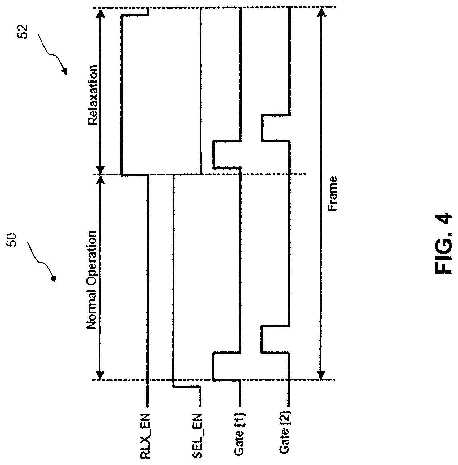
FIG. 4 illustrates a driving scheme for the display system 120 of FIG. 3. Referring to FIGS. 3-4, each frame time operation includes a normal operation cycle 50 and a relaxation cycle 52. The normal operation cycle 50 includes a programming cycle and a driving cycle as well understood by one of ordinary skill in the art. In the normal operation cycle 50, SEL_EN is high so that the switch transistors T1 and T4 are on, and RLX_EN is low so that the switch transistors T2 and T3 are off. In the normal operation cycle 50, SEL [i] (i: the row number, i=1, 2, . . .) is coupled to the gate driver 36 (Gate[i]) via the switch transistor T1, and RLX[i] is coupled to VGL (the off voltage of the gate driver) via the transistor T4. The gate driver 36 sequentially outputs a select signal for each row (Gate[1], Gate [2]). Based on the select signal and a programming data (e.g., Data [1], Data [2]), the display system 120 programs a selected pixel circuit and drives the OLED in the selected pixel circuit.
In the relaxation cycle 52, SEL_EN is low, and RLX_EN is high. The switch transistors T2 and T3 are on, and the switch transistors T1 and T4 are off. SEL[i] is coupled to VGL via the switch transistor T3, and RLX[i] is coupled to the gate driver 36 (Gate [i]) via the switch transistor T2. As a result, the relaxation switch transistor (e.g., 18 of FIG. 1) is on. The switch transistor coupled to the data line (e.g., 16 of FIG. 1) is off. The gate-source voltage of the driving transistor (e.g., 14 of FIG. 1) in the pixel circuit 32 becomes, for example, zero.
In the above example, the normal operation and the relaxation operation are implemented in one frame. In another example, the relaxation operation may be implemented in a different frame. In a further example, the relaxation operation may be implemented after an active time on which the display system displays a valid image.
A recovery driving scheme for improving pixel component stabilities is now described in detail. The recovery driving scheme uses a recovery operation to improve the display lifetime, including recovering the degradation of pixel components and reducing temporal non-uniformity of pixels. The recovery driving scheme may include the relaxation operation (FIGS. 1-4). The recovery operation may be implemented after a active time or in an active time.
FIG. 5 illustrates a recovery driving scheme for a display system in accordance with an embodiment of the present invention. The recovery driving scheme 150 of FIG. 5 includes an active time 152 and a recovery time 154 after the active time 152. In FIG. 5, "f(k)" (k=1, 2, . . . , n) represents an active frame. In FIG. 5, "fr(1)" (l=1, 2, . . . , m) represents a recovery frame. During the active time 152, the active frames f(1), f(2), . . . , f(n) are applied to a display. During the recovery time 154, the recovery frames fr(1), fr(2), . . . , fr(m) are applied to the display. The recovery driving scheme 150 is applicable to any displays and pixel circuits.
The active time 152 is a normal operation time on which the display system displays a valid image. Each active frame includes a programming cycle for programming a pixel associated with the valid image and a driving cycle for driving a light emitting device. The recovery time 154 is a time for recovering the display and not for showing the valid image.
For example, after a user turns off the display (i.e., turns off a normal image display function or mode), the recovery frames fr(1), . . . , fr(m) are applied to the display to turn over the pixel's components aging. The aging of the pixel elements includes, for example, threshold voltage shift of transistors and OLED luminance and/or electrical degradation. During the recovery frame fr(1), one can operate the display in the relaxation mode (described above) and/or a mode of reducing OLED luminance and electrical degradation.
FIG. 6 illustrates one example of pixel components to which the recovery driving scheme of FIG. 5 is applied. As shown in FIG. 6, a pixel circuit includes a driving transistor 2 and OLED 4, being coupled in series between a power supply VDD and a power supply VSS. In FIG. 6. the driving transistor 2 is coupled to the power supply VDD. The OLED 4 is coupled to the driving transistor at node B0 and the power supply line VSS. The gate terminal of the driving transistor 2, i.e., node A0, is charged by a programming voltage. The driving transistor 2 provides a current to the OLED 4.
At least one of VSS and VDD is controllable (changeable). In this example, VSS line is a controllable voltage line so that the voltage on VSS is changeable. VDD line may be a controllable voltage line so that the voltage on VDD is changeable. VSS and VDD lines may be shared by other pixel circuits.
It would be well understood by one of ordinary skill in the art that the pixel circuit may include components other than the driving transistor 2 and the OLED 4, such as a switch transistor for selecting the pixel circuit and providing a programming data on a data line to the pixel circuit, and a storage capacitor in which the programming data is stored.
FIG. 7 illustrates one example of recovery frames associated with the recovery deriving scheme of FIG. 5. The recovery time 154A of FIG. 7 corresponds to the recovery time 154 of FIG. 5, and includes initialization frames Y1 and stand by frames Y2. The initialization frames Y1 include frames C1 and C2. The stand by frames Y2 include frames C3, . . . , CK. The stand by frames Y2 are normal stand by frames.
Referring to FIGS. 6-7, during the first frame C1 in the initialization frames Y1, the display is programmed with a high voltage (VP_R) while VSS is high voltage (VSS_R) and VDD is at VDD_R. As a result, node A0 is charged to VP_R and node B0 is charged to VDD_R. Thus, the voltage at OLED 4 will be--(VSS_R-VDD_R). Considering that VSS_R is larger than VDD_R, the OLED 4 will be under negative bias which will help the OLED 4 to recover.
VSS_R is higher than VSS at a normal image programming and driving operation. VP-R may be higher than that of a general programming voltage VP.
During the second frame C2 in the initialization frames Y1, the display is programmed with gray zero while VDD and VSS preserve their previous value. At this point, the gate-source voltage (VGS) of the driving transistor 2 will be--VDD_R. Thus, the driving transistor 2 will recover from the aging. Moreover, this condition will help to reduce the differential aging among the pixels, by balancing the aging effect. If the state of each pixel is known, one can use different voltages instead of zero for each pixel at this stage. As a result, the negative voltage apply to each pixel will be different so that the recovery will be faster and more efficient.
Each pixel may be programmed with different negative recovery voltage, for example, based on the ageing profile (history of the pixel's aging) or a look up table.
In FIG. 7, the frame C2 is located after the frame C1. However, in another example, the frame C2 may be implemented before the frame C1.
The same technique can be applied to a pixel in which the OLED 4 is coupled to the drain of the driving transistor 2 as well.
FIG. 8 illustrates another example of recovery frames associated with the recovery deriving scheme of FIG. 5. The recovery time 154B of FIG. 8 corresponds to the recovery time 154 of FIG. 5, and includes balancing frames Y3 and the stand by frames Y4. The stand by frames Y4 include frames DJ, . . . , Dk. The stand by frames Y4 correspond to the stand by frames Y3 of FIG. 7. The balancing frames Y3 include frames D1, . . . , DJ-1.
During the recovery time 154B, the display runs on uncompensated mode for a number of frames D1-DJ-1 that can be selected based on the ON time of the display. In this mode, the part that aged more start recovering and the part that aged less will age. This will balance the display uniformity over time.
In the above example, the display has the recovery time (154 of FIG. 5) after the active time (152 of FIG. 5). However, in another example, an active frame is divided into programming, driving and relaxation/recovery cycles. FIG. 9 illustrates a further example of a driving scheme for a display in accordance with an embodiment of the present invention. The active frame 160 of FIG. 9 includes a programming cycle 162, a driving cycle 164, and a relaxation/recovery cycle 166. The driving scheme of FIG. 9 is applied to a pixel having the driving transistor 2 and the OLED 4 of FIG. 6.
Referring to FIGS. 6 and 9, during the programming cycle 162, the pixel is programmed with a required programming voltage VP. During the driving cycle 164, the driving transistor 2 provides current to the OLED 4 based on the programming voltage VP. After the driving cycle 164, the relaxation/recovery cycle 166 starts. During the relaxation/recovery cycle 166, the degradation of pixel components is recovered. In this example, the display system implements a recovery operation formed by a first operation cycle 170, a second operation cycle 172 and a third operation cycle 174.
During the first operation cycle 170, VSS goes to VSS_R, and so node B0 is charged to VP-VT (VT: threshold voltage of the driving transistor 4). During the first operation cycle 172, node A0 is charged to VP_R and so the gate voltage of the driving transistor 2 will be--(VP-VT-VP_R). As a result, the pixel with larger programming voltage during the driving cycle 164 will have a larger negative voltage across its gate-source voltage. This will results in faster recovery for the pixels at higher stress condition.
In another example, the display system may be in the relaxation mode during the relaxation/recovery cycle 166.
In a further example, the history of pixels' aging may be used. If the history of the pixel's aging is known, each pixel can be programmed with different negative recovery voltage according to its aging profile. This will result in faster and more effective recovery. The negative recovery voltage is calculated or fetch from a look up table, based on the aging of the each pixel. In the above embodiments, the pixel circuits and display systems are described using n-type transistors. However, one of ordinary skill in the art would appreciate that the n-type transistor in the circuits can be replaced with a p-type transistor with complementary circuit concept. One of ordinary skill in the art would appreciate that the programming, driving and relaxation techniques in the embodiments are also applicable to a complementary pixel circuit having p-type transistors.
1. Some semiconductor devices experience stress annealing or recovery under certain bias, temperature and illumination.
2. For example, oxide semiconductor devices have negative threshold voltage shift under negative bias and illumination condition
3. Here higher energy photons (e.g., in the blue or UV range) can accelerate the negative threshold voltage shift.
Therefore, in one aspect of this invention, a semiconductor device is negatively biased while it is under illumination to induce negative threshold voltage shift in the device.
In another aspect of this invention, a semiconductor device can generate the light by itself to be used for recovery process.
In another aspect of the invention, the semiconductor device can be an array of the pixel and each pixel can be negatively biased and left under illumination.
In another aspect of the invention, the pixel can be biased with different biased levels based on a signal representing the performance of the pixel or aging history of the pixel. The signal can be the stress history, a current level for a given voltage, a voltage for a given current, or any other type of signal representing the pixel performance.
In one aspect of the invention, constant illumination and/or bias conditions are used for recovery.
In another aspect of the invention, pulse illumination and/or bias conditions are used for recovery.
In another aspect of the invention, the negative induced VT shift operation can be followed by stress condition with positive induced VT shift to minimize the gap between the performances of different pixels.
In another aspect of the invention, the negative induced VT shift and positive induced VT shift operations can be repeated multiple times.
Another aspect of this invention will be to use the bias illumination condition to improve non-uniformities associated with the solid state devices, including both initial non-uniformities and those due to aging.
One or more currently preferred embodiments have been described by way of example. It will be apparent to persons skilled in the art that a number of variations and modifications can be made without departing from the scope of the invention as defined in the claims.
* * * * *
D00000
D00001
D00002
D00003
D00004
D00005
D00006
D00007
D00008
XML
uspto.report is an independent third-party trademark research tool that is not affiliated, endorsed, or sponsored by the United States Patent and Trademark Office (USPTO) or any other governmental organization. The information provided by uspto.report is based on publicly available data at the time of writing and is intended for informational purposes only.
While we strive to provide accurate and up-to-date information, we do not guarantee the accuracy, completeness, reliability, or suitability of the information displayed on this site. The use of this site is at your own risk. Any reliance you place on such information is therefore strictly at your own risk.
All official trademark data, including owner information, should be verified by visiting the official USPTO website at www.uspto.gov. This site is not intended to replace professional legal advice and should not be used as a substitute for consulting with a legal professional who is knowledgeable about trademark law.