Compound of organic semiconductor and organic semiconductor device using the same
Kim , et al. April 27, 2
U.S. patent number 10,991,894 [Application Number 16/192,399] was granted by the patent office on 2021-04-27 for compound of organic semiconductor and organic semiconductor device using the same. This patent grant is currently assigned to FOUNDATION OF SOONGSIL UNIVERSITY-INDUSTRY COOPERATION, INDUSTRY-UNIVERSITY COOPERATION FOUNDATION HANYANG UNIVERSITY. The grantee listed for this patent is FOUNDATION OF SOONGSIL UNIVERSITY-INDUSTRY COOPERATION, Industry-University Cooperation Foundation Hanyang University. Invention is credited to Keun-Yeong Choi, Haejung Hwang, Moon Sung Kang, Do Hwan Kim, Hojin Lee, Han Wool Park, Ji Hye Shin.


View All Diagrams
| United States Patent | 10,991,894 |
| Kim , et al. | April 27, 2021 |
Compound of organic semiconductor and organic semiconductor device using the same
Abstract
Disclosed are an organic semiconductor compound that exhibits chemical resistance and etch resistance while maintaining electrical characteristics and thus is applicable to an existing photolithography process, thereby increasing process efficiency, and an organic semiconductor device using the same.
| Inventors: | Kim; Do Hwan (Anyang-si, KR), Lee; Hojin (Seoul, KR), Park; Han Wool (Seoul, KR), Choi; Keun-Yeong (Seoul, KR), Kang; Moon Sung (Seoul, KR), Hwang; Haejung (Seoul, KR), Shin; Ji Hye (Seoul, KR) | ||||||||||
|---|---|---|---|---|---|---|---|---|---|---|---|
| Applicant: |
|
||||||||||
| Assignee: | FOUNDATION OF SOONGSIL
UNIVERSITY-INDUSTRY COOPERATION (Seoul, KR) INDUSTRY-UNIVERSITY COOPERATION FOUNDATION HANYANG UNIVERSITY (Seoul, KR) |
||||||||||
| Family ID: | 1000005517066 | ||||||||||
| Appl. No.: | 16/192,399 | ||||||||||
| Filed: | November 15, 2018 |
Prior Publication Data
| Document Identifier | Publication Date | |
|---|---|---|
| US 20190157573 A1 | May 23, 2019 | |
Related U.S. Patent Documents
| Application Number | Filing Date | Patent Number | Issue Date | ||
|---|---|---|---|---|---|
| 15578483 | 10529937 | ||||
| PCT/KR2017/006734 | Jun 26, 2017 | ||||
| 14986852 | Jan 4, 2016 | 10164190 | |||
Foreign Application Priority Data
| Mar 19, 2015 [KR] | 10-2015-0038424 | |||
| Jul 10, 2015 [KR] | 10-2015-0098309 | |||
| Jun 27, 2016 [KR] | 10-2016-0079962 | |||
| Jun 30, 2016 [KR] | 10-2016-0082390 | |||
| Dec 7, 2016 [WO] | PCT/KR2016/014290 | |||
| Jan 13, 2017 [WO] | PCT/KR2017/000461 | |||
| Jun 22, 2017 [KR] | 10-2017-0079382 | |||
| Current U.S. Class: | 1/1 |
| Current CPC Class: | H01L 51/009 (20130101); H01L 51/0558 (20130101); B01J 20/226 (20130101); H01L 51/0084 (20130101); H01L 51/0094 (20130101); H01L 51/0028 (20130101); B01D 2253/204 (20130101); H01L 51/0541 (20130101) |
| Current International Class: | H01L 51/00 (20060101); B01J 20/22 (20060101); H01L 51/05 (20060101) |
References Cited [Referenced By]
U.S. Patent Documents
| 4946710 | August 1990 | Miller |
| 6433359 | August 2002 | Kelley et al. |
| 6653701 | November 2003 | Yamazaki |
| 6833180 | December 2004 | Kodemura |
| 7572667 | August 2009 | Ryu et al. |
| 7800101 | September 2010 | Song et al. |
| 8114704 | February 2012 | Kim et al. |
| 2004/0075120 | April 2004 | Wu |
| 2004/0195563 | October 2004 | Bao |
| 2005/0056828 | March 2005 | Wada |
| 2006/0231827 | October 2006 | Hanato et al. |
| 2007/0152370 | July 2007 | Roberts |
| 2010/0006824 | January 2010 | Hong et al. |
| 2010/0147365 | June 2010 | DeSimone |
| 2010/0264404 | October 2010 | Myung-Seok et al. |
| 2010/0288635 | November 2010 | Komiya |
| 2011/0049481 | March 2011 | Xavier |
| 2011/0049560 | March 2011 | Li |
| 2011/0301276 | December 2011 | Katayama et al. |
| 2013/0203198 | August 2013 | Min |
| 2013/0234116 | September 2013 | Lee |
| 2013/0345370 | December 2013 | Ona et al. |
| 2014/0183507 | July 2014 | Benwadih |
| 2015/0114814 | April 2015 | Suzuki |
| 2015/0122314 | May 2015 | Snaith |
| 2016/0276590 | September 2016 | Kim et al. |
| 101230265 | Jul 2008 | CN | |||
| 102015900 | Apr 2011 | CN | |||
| 102969277 | Mar 2013 | CN | |||
| 2007-019121 | Jan 2007 | JP | |||
| 2008-153354 | Jul 2008 | JP | |||
| 2004-0029143 | Apr 2004 | KR | |||
| 10-0668615 | Jan 2007 | KR | |||
| 10-0708720 | Apr 2007 | KR | |||
| 10-0737293 | Jul 2007 | KR | |||
| 10-0865500 | Oct 2008 | KR | |||
| 10-2009-0064514 | Jun 2009 | KR | |||
| 2010-0006294 | Jan 2010 | KR | |||
| 10-2010-0055410 | May 2010 | KR | |||
| 10-1174871 | Aug 2012 | KR | |||
| 2012-0095965 | Aug 2012 | KR | |||
| 10-1195550 | Oct 2012 | KR | |||
| 2013-0012823 | Feb 2013 | KR | |||
| 10-2014-0033466 | Mar 2014 | KR | |||
| 2014-0081249 | Jul 2014 | KR | |||
| 10-1508780 | Apr 2015 | KR | |||
| 2016-0055334 | May 2016 | KR | |||
| 10-1685071 | Dec 2016 | KR | |||
| 2008/090828 | Jul 2008 | WO | |||
| 20120164282 | Dec 2012 | WO | |||
Other References
|
C R. Kagan, D. B. Mitzi, C. D. Dmitrakopoulos, "Organic-Inorganic hybrid materials as semiconducting channels in thin-film field-effect transistors", Science, 286, p. 945-947 (Year: 1999). cited by examiner . M. W. A. MacLean, et al., "Unraveling inter- and intrachain electronics in polythiophene assemblies mediated by coordination nanospaces", Angewandte Chemie International Edition, 55, p. 708-718 (Year: 2016). cited by examiner . G. Yu et al., "Polymer photovoltaic cells: Enhanced efficiencies via a network of internal donor-acceptor heterojunctions", Science, 270, p. 1789-1791 (Year: 1995). cited by examiner . European Search Report for 15203122.5 dated Jul. 15, 2016. cited by applicant . M.F. Calhoun "Electronic functionalization of the surface of organic semiconductors with self-assembled monolayers" Department of Physics and Astronomy, Rutgers University, Nov. 18, 2007, p. 84-89. cited by applicant . M. Contstantinou et al. "Interface Passivation and Trap Reduction via a Solution-Based Method for Near-Zero ZHyswteresis Nanowire Field-Effect Transistors" ACS Appl. Mater. Interfaces 2015, 7, 22115-22120. cited by applicant . International Search Report PCT/ISA/210 for International Application No. PCT/KR2017/000461 dated Apr. 14, 2017. cited by applicant . Written Opinion of the International Searching Authority PCT/ISA/237 for International Application No. PCT/KR2017/000461 dated Apr. 14, 2017. cited by applicant . International Search Report PCT/ISA/210 for International Application No. PCT/KR2016/014290 dated Mar. 9, 2017. cited by applicant . Written Opinion of the International Searching Authority PCT/ISA/237 for International Application No. PCT/KR2016/014290 dated Mar. 9, 2017. cited by applicant. |
Primary Examiner: Smith; Eric R
Attorney, Agent or Firm: Sughrue Mion, PLLC
Claims
The invention claimed is:
1. An organic semiconductor compound, comprising: a precursor structure; and an organic semiconductor, wherein the organic semiconductor penetrates the precursor structure to form a three-dimensional network structure, wherein the precursor structure is formed by gelating an organometallic precursor by hydrolysis and condensation reaction, wherein the organometallic precursor is represented by Formula 1 below: ##STR00007## wherein M1 and M2 each independently comprise at least one of Sc, Ti, V, Cr, Mn, Fe, Co, Ni, Si, Cu, Zn, Pd, Ag, Au, Hg, Pt, Ta, Mo, Zr, Ta, Mg, Sn, Ge, Y, Nb, Tc, Ru, Rh, Lu, Hf, W, Re, Os, Ir, Lr, Rf, Db, Sg, Bh, Hs, Mt, Ds, Rg, and Uub, Y is one of a substituted or unsubstituted C1 to C30 alkyl group, a C3 to C30 cycloalkyl group, a C3 to C30 heterocyclic group, a C2 to C30 alkenyl group, a C3 to C30 cycloalkenyl group, a C2 to C30 alkynyl group, a C1 to C30 alkoxy group, a C1 to C30 alkylthio group, a C3 to C30 arylether group, a C3 to C30 arylthioether group, a C3 to C30 aryl group, a C3 to C30 heteroaryl group, a halogen atom, a cyano group, a formyl group, a C1 to C30 alkylcarbonyl group, a C3 to C30 arylcarbonyl group, a carboxyl group, a C1 to C30 alkoxycarbonyl group, a C3 to C30 aryloxycarbonyl group, a C1 to C30 alkylcarbonyloxy group, a C1 to C30 arylcarbonyloxy group, a carbamoyl group, an amino group, and a silyl group, and X1 and X2 are each independently one selected from the group consisting of a hydrogen atom, a substituted or unsubstituted C1 to C30 alkyl group, a C3 to C30 cycloalkyl group, a C3 to C30 heterocyclic group, a C2 to C30 alkenyl group, a C3 to C30 cycloalkenyl group, a C2 to C30 alkynyl group, a C1 to C30 alkoxy group, a C1 to C30 alkylthio group, a C3 to C30 arylether group, a C3 to C30 arylthioether group, a C3 to C30 aryl group, a C3 to C30 heteroaryl group, a halogen atom, a cyano group, a formyl group, a C1 to C30 alkylcarbonyl group, a C3 to C30 arylcarbonyl group, a carboxyl group, a C1 to C30 alkoxycarbonyl group, a C3 to C30 aryloxycarbonyl group, a C1 to C30 alkylcarbonyloxy group, a C1 to C30 arylcarbonyloxy group, a carbamoyl group, an amino group, and a hydroxyl group, wherein the substituted alkyl group comprises an alkyl group substituted with a halogen element.
2. The organic semiconductor compound according to claim 1, wherein the organic semiconductor is solated by being dissolved in an organic solvent.
3. An organic semiconductor device, comprising: a substrate; an organic semiconductor layer formed on the substrate and comprising the organic semiconductor compound according to claim 1; and a self-assembled monolayer formed on the organic semiconductor layer using a self-assembling precursor, wherein reactive groups are comprised on an upper surface of the organic semiconductor layer, and the self-assembled monolayer is formed through a chemical bond between the reactive groups and the self-assembling precursor.
4. The organic semiconductor device according to claim 3, wherein functional groups are comprised on an upper surface of the self-assembled monolayer, and the functional groups of the self-assembled monolayer are different from the reactive groups of the organic semiconductor layer.
5. The organic semiconductor device according to claim 3, further comprising an insulating layer formed between the substrate and the organic semiconductor layer, wherein the organic semiconductor layer is formed through a chemical bond between the organometallic precursor and functional groups on the insulating layer.
6. The organic semiconductor device according to claim 5, further comprising: a gate pattern formed between the substrate and the insulating layer; and source/drain patterns formed on the organic semiconductor layer.
7. The organic semiconductor device according to claim 3, further comprising: an insulating layer formed on the self-assembled monolayer; a gate pattern formed on the insulating layer; and source/drain patterns formed between the substrate and the organic semiconductor layer.
8. The organic semiconductor device according to claim 3, wherein the self-assembling precursor is represented by Formula 2 below: ##STR00008## wherein A comprises one of NH.sub.2, CH.sub.3, --SH, --COOH, CF.sub.3, and a halogen element, the halogen element comprising one of F, C1, Br, and I, R is one selected from the group consisting of a substituted or unsubstituted C1 to C30 alkyl group, a C3 to C30 cycloalkyl group, a C3 to C30 heterocyclic group, a C2 to C30 alkenyl group, a C3 to C30 cycloalkenyl group, a C2 to C30 alkynyl group, a C1 to C30 alkoxy group, a C1 to C30 alkylthio group, a C3 to C30 arylether group, a C3 to C30 arylthioether group, a substituted or unsubstituted C3 to C30 aryl group, a C3 to C30 heteroaryl group, halogen atom, a cyano group, a formyl group, a C1 to C30 alkylcarbonyl group, a C3 to C30 arylcarbonyl group, a carboxyl group, a C1 to C30 alkoxycarbonyl group, a C3 to C30 aryloxycarbonyl group, a C1 to C30 alkylcarbonyloxy group, a C1 to C30 arylcarbonyloxy group, a carbamoyl group, a substituted or unsubstituted thiophene, an amino group, and a hydroxyl group, n is an integer of 0 to 30, M3 is one of Sc, Ti, V, Cr, Mn, Fe, Co, Ni, Si, Cu, Zn, Pd, Ag, Au, Hg, Pt, Ta, Mo, Zr, Ta, Mg, Sn, Ge, Y, Nb, Tc, Ru, Rh, Lu, Hf, W, Re, Os, Ir, Lr, Rf, Db, Sg, Bh, Hs, Mt, Ds, Rg, and Uub, and X3 are each independently one selected from the group consisting of a hydrogen atom, a substituted or unsubstituted C1 to C30 alkyl group, a C3 to C30 cycloalkyl group, a C3 to C30 heterocyclic group, a C2 to C30 alkenyl group, a C3 to C30 cycloalkenyl group, a C2 to C30 alkynyl group, a C1 to C30 alkoxy group, a C1 to C30 alkylthio group, a C3 to C30 arylether group, a C3 to C30 arylthioether group, a C3 to C30 aryl group, a C3 to C30 heteroaryl group, a halogen atom, a cyano group, a formyl group, a C1 to C30 alkylcarbonyl group, a C3 to C30 arylcarbonyl group, a carboxyl group, a C1 to C30 alkoxycarbonyl group, a C3 to C30 aryloxycarbonyl group, a C1 to C30 alkylcarbonyloxy group, a C1 to C30 arylcarbonyloxy group, a carbamoyl group, an amino group, and a hydroxyl group, wherein the substituted alkyl group of X3 comprises an alkyl group substituted with a halogen element.
9. The organic semiconductor device according to claim 3, wherein the chemical bond comprises a silanol bond.
Description
CROSS-REFERENCE TO RELATED APPLICATIONS
This application is a continuation-in-part of U.S. patent application Ser. No. 14/986,852, filed on Jan. 4, 2016, now U.S. Pat. No. 10/164,190, which claims priority from Korean Patent Application No. 10-2015-0038424 filed Mar. 19, 2015 and Korean Patent Application No. 10-2015-0098309 filed Jul. 10, 2015, and is a continuation-in-part of U.S. patent application Ser. No. 15/578,483, filed on Nov. 30, 2017, now U.S. Pat. No. 10/529,937, which is a National Stage Entry of International Application No. PCT/KR2017/006734 filed Jun. 26, 2017, which claims priority from Korean Patent Application No. 10-2016-0079962 filed Jun. 27, 2016, Korean Patent Application No. 10-2016-0082390 filed Jun. 30, 2016, PCT/KR2016/014290 filed Dec. 7, 2016, PCT/KR2017/000461 filed Jan. 13, 2017, and Korean Patent Application No. 10-2017-0079382 filed Jun. 22, 2017, the contents of all of the prior applications are incorporated herein by reference in their entireties.
TECHNICAL FIELD
The present invention relates to a semiconductor device, and more particularly, to an organic semiconductor compound and an organic semiconductor device using the same.
BACKGROUND ART
Recently, research into application of flexible materials to displays, thin-film solar cells, and the like has been actively conducted.
In fabricating such electronic devices, it may be advantageous to use an organic semiconductor instead of a conventional inorganic semiconductor.
Accordingly, interest in an organic semiconductor device wherein channels are formed using an organic semiconductor material is increasing.
However, since organic semiconductors are more sensitive to the external environment than inorganic semiconductors, there is a need to improve the electrical characteristics and durability of organic semiconductor devices.
RELATED ART DOCUMENTS
Patent Documents
Korean Patent No. 10-0865500, entitled "ORGANIC SEMICONDUCTOR MATERIAL AND ORGANIC SEMICONDUCTOR DEVICE USING THE SAME"
Korean Patent Application Publication No. 10-2009-0064514, entitled "ELECTRONIC DEVICE USING ORGANIC SEMICONDUCTOR DEVICE"
Korean Patent Application Publication No. 10-2010-0055410, entitled "METHOD OF FABRICATING ORGANIC SEMICONDUCTOR DEVICE, ORGANIC SEMICONDUCTOR DEVICE, AND ORGANIC SEMICONDUCTOR DEVICE"
DISCLOSURE
Technical Problem
Therefore, the present invention has been made in view of the above problems, and it is one object of the present invention to provide a semiconductor device, and more particularly, to an organic semiconductor compound and an organic semiconductor device having improved durability by using the same.
Technical Solution
In accordance with an aspect of the present invention, the above and other objects can be accomplished by the provision of an organic semiconductor compound including a precursor structure; and an organic semiconductor, wherein the precursor structure and the organic semiconductor penetrate each other to form a three-dimensional network structure.
In the organic semiconductor compound according to an embodiment of the present invention, the precursor structure may be formed by gelating an organometallic precursor by hydrolysis and condensation reaction.
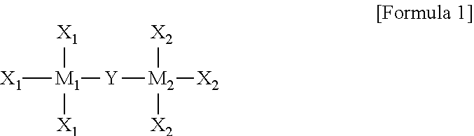
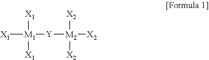
In the organic semiconductor compound according to an embodiment of the present invention, the organometallic precursor may be represented by Formula 1 below:
##STR00001##
wherein M1 and M2 each independently include at least one of Sc, Ti, V, Cr, Mn, Fe, Co, Ni, Si, Cu, Zn, Pd, Ag, Au, Hg, Pt, Ta, Mo, Zr, Ta, Mg, Sn, Ge, Y, Nb, Tc, Ru, Rh, Lu, Hf, W, Re, Os, Ir, Lr, Rf, Db, Sg, Bh, Hs, Mt, Ds, Rg, and Uub,
Y is one of a substituted or unsubstituted C1 to C30 alkyl group, a C3 to C30 cycloalkyl group, a C3 to C30 heterocyclic group, a C2 to C30 alkenyl group, a C3 to C30 cycloalkenyl group, a C2 to C30 alkynyl group, a C1 to C30 alkoxy group, a C1 to C30 alkylthio group, a C3 to C30 arylether group, a C3 to C30 arylthioether group, a C3 to C30 aryl group, a C3 to C30 heteroaryl group, a halogen atom, a cyano group, a formyl group, a C1 to C30 alkylcarbonyl group, a C3 to C30 arylcarbonyl group, a carboxyl group, a C1 to C30 alkoxycarbonyl group, a C3 to C30 aryloxycarbonyl group, a C1 to C30 alkylcarbonyloxy group, a C1 to C30 arylcarbonyloxy group, a carbamoyl group, an amino group, and a silyl group, and
X1 and X2 are each independently one selected from among a hydrogen atom, a substituted or unsubstituted C1 to C30 alkyl group, a C3 to C30 cycloalkyl group, a C3 to C30 heterocyclic group, a C2 to C30 alkenyl group, a C3 to C30 cycloalkenyl group, a C2 to C30 alkynyl group, a C1 to C30 alkoxy group, a C1 to C30 alkylthio group, a C3 to C30 arylether group, a C3 to C30 arylthioether group, a C3 to C30 aryl group, a C3 to C30 heteroaryl group, a halogen atom, a cyano group, a formyl group, a C1 to C30 alkylcarbonyl group, a C3 to C30 arylcarbonyl group, a carboxyl group, a C1 to C30 alkoxycarbonyl group, a C3 to C30 aryloxycarbonyl group, a C1 to C30 alkylcarbonyloxy group, a C1 to C30 arylcarbonyloxy group, a carbamoyl group, an amino group, and a hydroxyl group, wherein the substituted alkyl group includes an alkyl group substituted with a halogen element.
In the organic semiconductor compound according to an embodiment of the present invention, the organic semiconductor may be solated by being dissolved in an organic solvent.
In accordance with another aspect of the present invention, there is provided an organic semiconductor device including a substrate; an organic semiconductor layer formed on the substrate and including the organic semiconductor compound; and a self-assembled monolayer formed on the organic semiconductor layer using a self-assembling precursor, wherein reactive groups are included on an upper surface of the organic semiconductor layer, and the self-assembled monolayer is formed through a chemical bond between the reactive groups and the self-assembling precursor.
In the organic semiconductor device according to another embodiment of the present invention, functional groups may be included on an upper surface of the self-assembled monolayer, and the functional groups of the self-assembled monolayer may be different from the reactive groups of the organic semiconductor layer.
In the organic semiconductor device according to another embodiment of the present invention, the organic semiconductor layer may be formed using an organometallic precursor represented by Formula 1 below:
##STR00002##
wherein M1 and M2 each independently include at least one of Sc, Ti, V, Cr, Mn, Fe, Co, Ni, Si, Cu, Zn, Pd, Ag, Au, Hg, Pt, Ta, Mo, Zr, Ta, Mg, Sn, Ge, Y, Nb, Tc, Ru, Rh, Lu, Hf, W, Re, Os, Ir, Lr, Rf, Db, Sg, Bh, Hs, Mt, Ds, Rg, and Uub,
Y is one of a substituted or unsubstituted C1 to C30 alkyl group, a C3 to C30 cycloalkyl group, a C3 to C30 heterocyclic group, a C2 to C30 alkenyl group, a C3 to C30 cycloalkenyl group, a C2 to C30 alkynyl group, a C1 to C30 alkoxy group, a C1 to C30 alkylthio group, a C3 to C30 arylether group, a C3 to C30 arylthioether group, a C3 to C30 aryl group, a C3 to C30 heteroaryl group, a halogen atom, a cyano group, a formyl group, a C1 to C30 alkylcarbonyl group, a C3 to C30 arylcarbonyl group, a carboxyl group, a C1 to C30 alkoxycarbonyl group, a C3 to C30 aryloxycarbonyl group, a C1 to C30 alkylcarbonyloxy group, a C1 to C30 arylcarbonyloxy group, a carbamoyl group, an amino group, and a silyl group, and
X1 and X2 are each independently one selected from among a hydrogen atom, a substituted or unsubstituted C1 to C30 alkyl group, a C3 to C30 cycloalkyl group, a C3 to C30 heterocyclic group, a C2 to C30 alkenyl group, a C3 to C30 cycloalkenyl group, a C2 to C30 alkynyl group, a C1 to C30 alkoxy group, a C1 to C30 alkylthio group, a C3 to C30 arylether group, a C3 to C30 arylthioether group, a C3 to C30 aryl group, a C3 to C30 heteroaryl group, a halogen atom, a cyano group, a formyl group, a C1 to C30 alkylcarbonyl group, a C3 to C30 arylcarbonyl group, a carboxyl group, a C1 to C30 alkoxycarbonyl group, a C3 to C30 aryloxycarbonyl group, a C1 to C30 alkylcarbonyloxy group, a C1 to C30 arylcarbonyloxy group, a carbamoyl group, an amino group, and a hydroxyl group, wherein the substituted alkyl group includes an alkyl group substituted with a halogen element.
The organic semiconductor device according to another embodiment of the present invention may further include an insulating layer formed between the substrate and the organic semiconductor layer, wherein the organic semiconductor layer is formed through a chemical bond between the organometallic precursor and functional groups on the insulating layer.
The organic semiconductor device according to another embodiment of the present invention may further include a gate pattern formed between the substrate and the insulating layer; and source/drain patterns formed on the organic semiconductor layer.
The organic semiconductor device according to another embodiment of the present invention may further include an insulating layer formed on the self-assembled monolayer; a gate pattern formed on the insulating layer; and source/drain patterns formed between the substrate and the organic semiconductor layer.
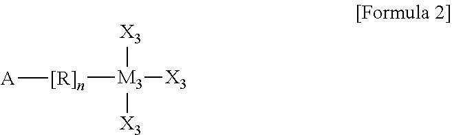
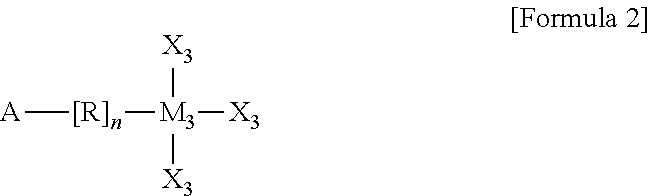
In the organic semiconductor device according to another embodiment of the present invention, the self-assembling precursor may be represented by Formula 2 below:
##STR00003##
wherein A includes one of --NH2, --CH3, --SH, --COOH, --CF3, and a halogen element, the halogen element including one of F, Cl, Br, and I,
R is one selected from among a substituted or unsubstituted C1 to C30 alkyl group, a C3 to C30 cycloalkyl group, a C3 to C30 heterocyclic group, a C2 to C30 alkenyl group, a C3 to C30 cycloalkenyl group, a C2 to C30 alkynyl group, a C1 to C30 alkoxy group, a C1 to C30 alkylthio group, a C3 to C30 arylether group, a C3 to C30 arylthioether group, a substituted or unsubstituted C3 to C30 aryl group, a C3 to C30 heteroaryl group, halogen atom, a cyano group, a formyl group, a C1 to C30 alkylcarbonyl group, a C3 to C30 arylcarbonyl group, a carboxyl group, a C1 to C30 alkoxycarbonyl group, a C3 to C30 aryloxycarbonyl group, a C1 to C30 alkylcarbonyloxy group, a C1 to C30 arylcarbonyloxy group, a carbamoyl group, a substituted or unsubstituted thiophene, an amino group, and a hydroxyl group,
n is an integer of 0 to 30,
M3 is one of Sc, Ti, V, Cr, Mn, Fe, Co, Ni, Si, Cu, Zn, Pd, Ag, Au, Hg, Pt, Ta, Mo, Zr, Ta, Mg, Sn, Ge, Y, Nb, Tc, Ru, Rh, Lu, Hf, W, Re, Os, Jr, Lr, Rf, Db, Sg, Bh, Hs, Mt, Ds, Rg, and Uub, and
X3 are each independently one selected from among a hydrogen atom, a substituted or unsubstituted C1 to C30 alkyl group, a C3 to C30 cycloalkyl group, a C3 to C30 heterocyclic group, a C2 to C30 alkenyl group, a C3 to C30 cycloalkenyl group, a C2 to C30 alkynyl group, a C1 to C30 alkoxy group, a C1 to C30 alkylthio group, a C3 to C30 arylether group, a C3 to C30 arylthioether group, a C3 to C30 aryl group, a C3 to C30 heteroaryl group, a halogen atom, a cyano group, a formyl group, a C1 to C30 alkylcarbonyl group, a C3 to C30 arylcarbonyl group, a carboxyl group, a C1 to C30 alkoxycarbonyl group, a C3 to C30 aryloxycarbonyl group, a C1 to C30 alkylcarbonyloxy group, a C1 to C30 arylcarbonyloxy group, a carbamoyl group, an amino group, and a hydroxyl group, wherein the substituted alkyl group of X3 includes an alkyl group substituted with a halogen element.
In the organic semiconductor device according to another embodiment of the present invention, the chemical bond may include a silanol bond.
Advantageous Effects
As apparent from the above description, an organic semiconductor compound according to an embodiment of the present invention exhibits chemical resistance and etching resistance while maintaining optoelectrical characteristics, thereby being applicable to an existing photolithography process and increasing process efficiency.
Various materials included in an organic semiconductor device according to another embodiment of the present invention can combine and interact with functional groups of a self-assembling precursor, thereby increasing binding force of an insulating layer and an organic semiconductor layer. Accordingly, current-voltage characteristics (current increase, threshold voltage control) of an organic semiconductor device can be improved.
An organic semiconductor device according to another embodiment of the present invention can induce strong binding of an interface between an insulator including a silanol bond on a surface thereof and a gelated organic semiconductor layer, thereby securing interface stability against external mechanical stimuli and thus being easily applied to flexible electronic devices.
DESCRIPTION OF DRAWINGS
The application file contains at least one drawing executed in color. Copies of this application publication with the color drawings will be provided by the Office upon request and payment of the necessary fee.
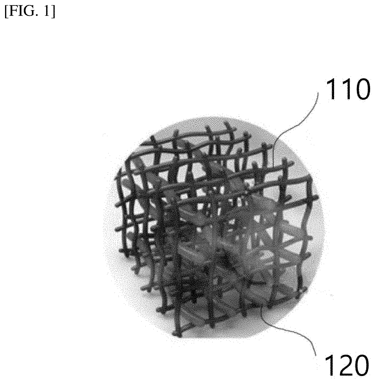
FIG. 1 is a schematic diagram illustrating the structure of an organic semiconductor compound according to an embodiment of the present invention.
FIGS. 2A, 3A, 4A, 5A, and 6A are sectional views sequentially illustrating a process of fabricating an organic semiconductor device according to another embodiment of the present invention. In addition, FIGS. 2B, 3B, 4B, 5B, and 6B respectively illustrate B regions of FIGS. 2A, 3A, 4A, 5A, and 6A.
BEST MODE
The present invention will now be described more fully with reference to the accompanying drawings and contents disclosed in the drawings. However, the present invention should not be construed as limited to the exemplary embodiments described herein.
The terms used in the present specification are used to explain a specific exemplary embodiment and not to limit the present inventive concept. Thus, the expression of singularity in the present specification includes the expression of plurality unless clearly specified otherwise in context.
It will be further understood that the terms "comprise" and/or "comprising", when used in this specification, specify the presence of stated components, steps, operations, and/or elements, but do not preclude the presence or addition of one or more other components, steps, operations, and/or elements thereof.
It should not be understood that arbitrary aspects or designs disclosed in "embodiments", "examples", "aspects", etc. used in the specification are more satisfactory or advantageous than other aspects or designs.
In addition, the expression "or" means "inclusive or" rather than "exclusive or". That is, unless otherwise mentioned or clearly inferred from context, the expression "x uses a or b" means any one of natural inclusive permutations.
In addition, as used in the description of the invention and the appended claims, the singular forms "a", "an" and "the" are intended to include the plural forms as well, unless context clearly indicates otherwise.
Although terms used in the specification are selected from terms generally used in related technical fields, other terms may be used according to technical development and/or due to change, practices, priorities of technicians, etc.
Therefore, it should not be understood that terms used below limit the technical spirit of the present invention, and it should be understood that the terms are exemplified to describe embodiments of the present invention.
Also, some of the terms used herein may be arbitrarily chosen by the present applicant. In this case, these terms are defined in detail below. Accordingly, the specific terms used herein should be understood based on the unique meanings thereof and the whole context of the present invention.
Meanwhile, terms such as "first" and "second" are used herein merely to describe a variety of constituent elements, but the constituent elements are not limited by the terms. The terms are used only for the purpose of distinguishing one constituent element from another constituent element.
In addition, when an element such as a layer, a film, a region, and a constituent is referred to as being "on" another element, the element can be directly on another element or an intervening element can be present.
Unless otherwise defined, all terms (including technical and scientific terms) used herein have the same meaning as commonly understood by one of ordinary skill in the art. It will be further understood that terms, such as those defined in commonly used dictionaries, should be interpreted as having a meaning that is consistent with their meaning in the context of the relevant art and the present invention, and will not be interpreted in an idealized or overly formal sense unless expressly so defined herein.
Meanwhile, in the following description of the present invention, a detailed description of known functions and configurations incorporated herein will be omitted when it may make the subject matter of the present invention unclear.
The terms used in the specification are defined in consideration of functions used in the present invention, and can be changed according to the intent or conventionally used methods of clients, operators, and users. Accordingly, definitions of the terms should be understood on the basis of the entire description of the present specification.
Hereinafter, embodiments of the present invention are more fully described with reference to the accompanying drawings.
FIG. 1 is a schematic diagram illustrating the structure of an organic semiconductor compound according to an embodiment of the present invention.
Referring to FIG. 1, a final product of the organic semiconductor compound according to an embodiment of the present invention may have a three-dimensional network structure wherein an organic semiconductor 120 passes through gaps of a precursor 110 having a two-dimensional lattice structure.
In addition, the structure of the precursor 110 is not limited to the two-dimensional lattice structure and may be a random structure.
When the precursor 110 has a random structure, the precursor 110 and the organic semiconductor 120 may penetrate each other to form a three-dimensional network structure, instead of the organic semiconductor 120 orthogonally passing through gaps of the precursor 110.
Accordingly, hardness of the organic semiconductor compound may be controlled by adjusting ratios of the precursor 110 and the organic semiconductor 120 according to the purpose of a user.
An organometallic precursor may be formed to have a ladder-like two-dimensional structure in a step of gelating the same by hydrolysis and condensation reaction.
When a precursor is gelated, the precursor may be formed to have a ladder-like two-dimensional structure at a specific temperature (70.degree. C. to 90.degree. C.).
Here, the organometallic precursor may include a metal (M) and a reactive group (X). Here, the reactive group may be formed by synthesizing various substances according to purpose.
Accordingly, in the step of gelating an organometallic precursor, the organometallic precursor may be gelated to have a two-dimensional lattice structure through a gelation process including hydrolysis and condensation reaction.
In general, the metal may include one or more metals selected from the group consisting of Sc, Ti, V, Cr, Mn, Fe, Co, Ni, Si, Cu, Zn, Pd, Ag, Au, Hg, Pt, Ta, Mo, Zr, Ta, Mg, Sn, Ge, Y, Nb, Tc, Ru, Rh, Lu, Hf, W, Re, Os, Ir, Lr, Rf, Db, Sg, Bh, Hs, Mt, Ds, Rg, and Uub.
In addition, the reactive group (X) may be selected from among a hydrogen atom, an alkyl group, a cycloalkyl group, a heterocyclic group, an alkenyl group, a cycloalkenyl group, an alkynyl group, an alkoxy group, an alkylthio group, an arylether group, an arylthioether group, an aryl group, a heteroaryl group, a halogen atom, a cyano group, a formyl group, an alkylcarbonyl group, an arylcarbonyl group, a carboxyl group, an alkoxycarbonyl group, an aryloxycarbonyl group, an alkylcarbonyloxy group, an arylcarbonyloxy group, a carbamoyl group, an amino group, and a silyl group.
More particularly, the organometallic precursor may be represented by Formula 1 below.
##STR00004##
wherein M1 and M2 each independently include at least one of Sc, Ti, V, Cr, Mn, Fe, Co, Ni, Si, Cu, Zn, Pd, Ag, Au, Hg, Pt, Ta, Mo, Zr, Ta, Mg, Sn, Ge, Y, Nb, Tc, Ru, Rh, Lu, Hf, W, Re, Os, Ir, Lr, Rf, Db, Sg, Bh, Hs, Mt, Ds, Rg, and Uub,
Y is one of a substituted or unsubstituted C1 to C30 alkyl group, a C3 to C30 cycloalkyl group, a C3 to C30 heterocyclic group, a C2 to C30 alkenyl group, a C3 to C30 cycloalkenyl group, a C2 to C30 alkynyl group, a C1 to C30 alkoxy group, a C1 to C30 alkylthio group, a C3 to C30 arylether group, a C3 to C30 arylthioether group, a C3 to C30 aryl group, a C3 to C30 heteroaryl group, a halogen atom, a cyano group, a formyl group, a C1 to C30 alkylcarbonyl group, a C3 to C30 arylcarbonyl group, a carboxyl group, a C1 to C30 alkoxycarbonyl group, a C3 to C30 aryloxycarbonyl group, a C1 to C30 alkylcarbonyloxy group, a C1 to C30 arylcarbonyloxy group, a carbamoyl group, an amino group, and a silyl group, and
X1 and X2 are each independently one selected from among a hydrogen atom, a substituted or unsubstituted C1 to C30 alkyl group, a C3 to C30 cycloalkyl group, a C3 to C30 heterocyclic group, a C2 to C30 alkenyl group, a C3 to C30 cycloalkenyl group, a C2 to C30 alkynyl group, a C1 to C30 alkoxy group, a C1 to C30 alkylthio group, a C3 to C30 arylether group, a C3 to C30 arylthioether group, a C3 to C30 aryl group, a C3 to C30 heteroaryl group, a halogen atom, a cyano group, a formyl group, a C1 to C30 alkylcarbonyl group, a C3 to C30 arylcarbonyl group, a carboxyl group, a C1 to C30 alkoxycarbonyl group, a C3 to C30 aryloxycarbonyl group, a C1 to C30 alkylcarbonyloxy group, a C1 to C30 arylcarbonyloxy group, a carbamoyl group, an amino group, and a hydroxyl group, wherein the substituted alkyl group includes an alkyl group substituted with a halogen element.
In accordance with an embodiment of the present invention, Formula 1, at least one of X.sub.1 and X.sub.2 may be a C1 to C30 alkoxy group, a C1 to C30 alkylthio group, a C3 to C30 arylether group, a C3 to C30 arylthioether group, a C3 to C30 aryl group, a C3 to C30 heteroaryl group, a halogen atom, a cyano group, a formyl group, a C1 to C30 alkylcarbonyl group, a C3 to C30 arylcarbonyl group, a carboxyl group, a C1 to C30 alkoxycarbonyl group, a C3 to C30 aryloxycarbonyl group, a C1 to C30 alkylcarbonyloxy group, a C1 to C30 arylcarbonyloxy group, a carbamoyl group, an amino group, and a hydroxyl group.
In addition, in accordance with an embodiment of the present invention, in Formula 1, at least one of X.sub.1 and at least one of X2 may be each independently a C1 to C30 alkoxy group, a C1 to C30 alkylthio group, a C3 to C30 arylether group, a C3 to C30 arylthioether group, a C3 to C30 aryl group, a C3 to C30 heteroaryl group, a halogen atom, a cyano group, a formyl group, a C1 to C30 alkylcarbonyl group, a C3 to C30 arylcarbonyl group, a carboxyl group, a C1 to C30 alkoxycarbonyl group, a C3 to C30 aryloxycarbonyl group, a C1 to C30 alkylcarbonyloxy group, a C1 to C30 arylcarbonyloxy group, a carbamoyl group, an amino group, and a hydroxyl group.
The organometallic precursor may include the first reactive groups X bonded with an inorganic element. The inorganic element may be denoted as M.sub.1 and M.sub.2 in Formula 1. The first reactive group (X) may be at least one of groups denoted as X.sub.1 and X.sub.2 in Formula 1. The first reactive group (X) may include at least one of a C1 to C30 alkoxy group, a C1 to C30 alkylthio group, a C3 to C30 arylether group, a C3 to C30 arylthioether group, a C3 to C30 aryl group, a C3 to C30 heteroaryl group, a halogen atom, a cyano group, a formyl group, a C1 to C30 alkylcarbonyl group, a C3 to C30 arylcarbonyl group, a carboxyl group, a C1 to C30 alkoxycarbonyl group, a C3 to C30 aryloxycarbonyl group, a C1 to C30 alkylcarbonyloxy group, a C1 to C30 arylcarbonyloxy group, a carbamoyl group, an amino group, and a hydroxyl group.
The gelated organometallic precursor 110 may include a plurality of organometallic precursors. These organometallic precursors may react with each other, thereby forming a two-dimensional lattice structure.
The organic semiconductor 120 may be dissolved in an organic solvent, thereby being solated. Here, the organic solvent may include one of chloroform, dichloromethane, acetone, pyridine, tetrahydrofuran, chlorobenzene, toluene, and dichlorobenzene or a mixture thereof.
Next, an organic semiconductor compound having a three-dimensional network structure wherein the solated organic semiconductor 120 orthogonally passes through gaps of a lattice structure of the gelated organometallic precursor 110 may be formed by stirring the gelated organometallic precursor 110 having a two-dimensional lattice structure and the solated organic semiconductor 120 while maintaining a certain temperature.
Here, the solated organic semiconductor and the gelated precursor may be stirred at about 80.degree. C., but the present invention is not limited thereto.
Hereinafter, an organic semiconductor device according to another embodiment of the present invention is described in detail with reference to FIGS. 2A to 6B.
Through the following detailed description of a fabrication method, the bonding and structure of each layer constituting the organic semiconductor device can be confirmed in detail
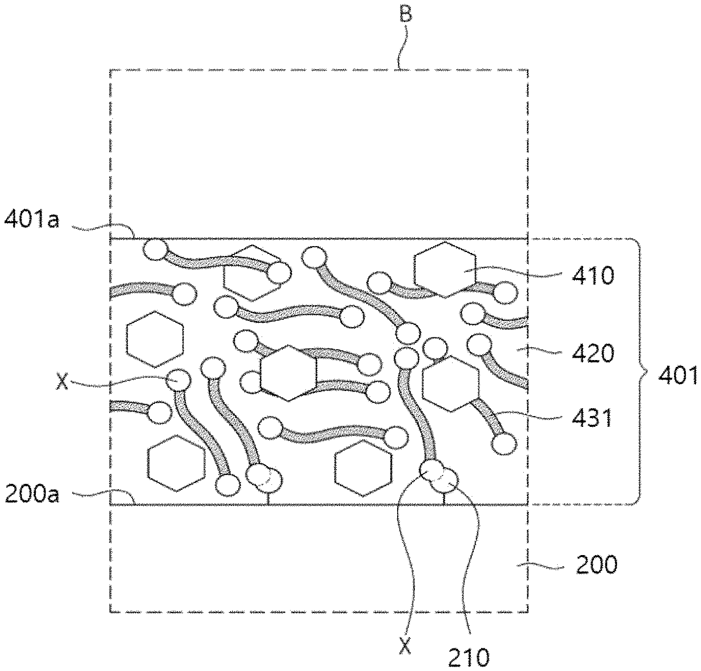
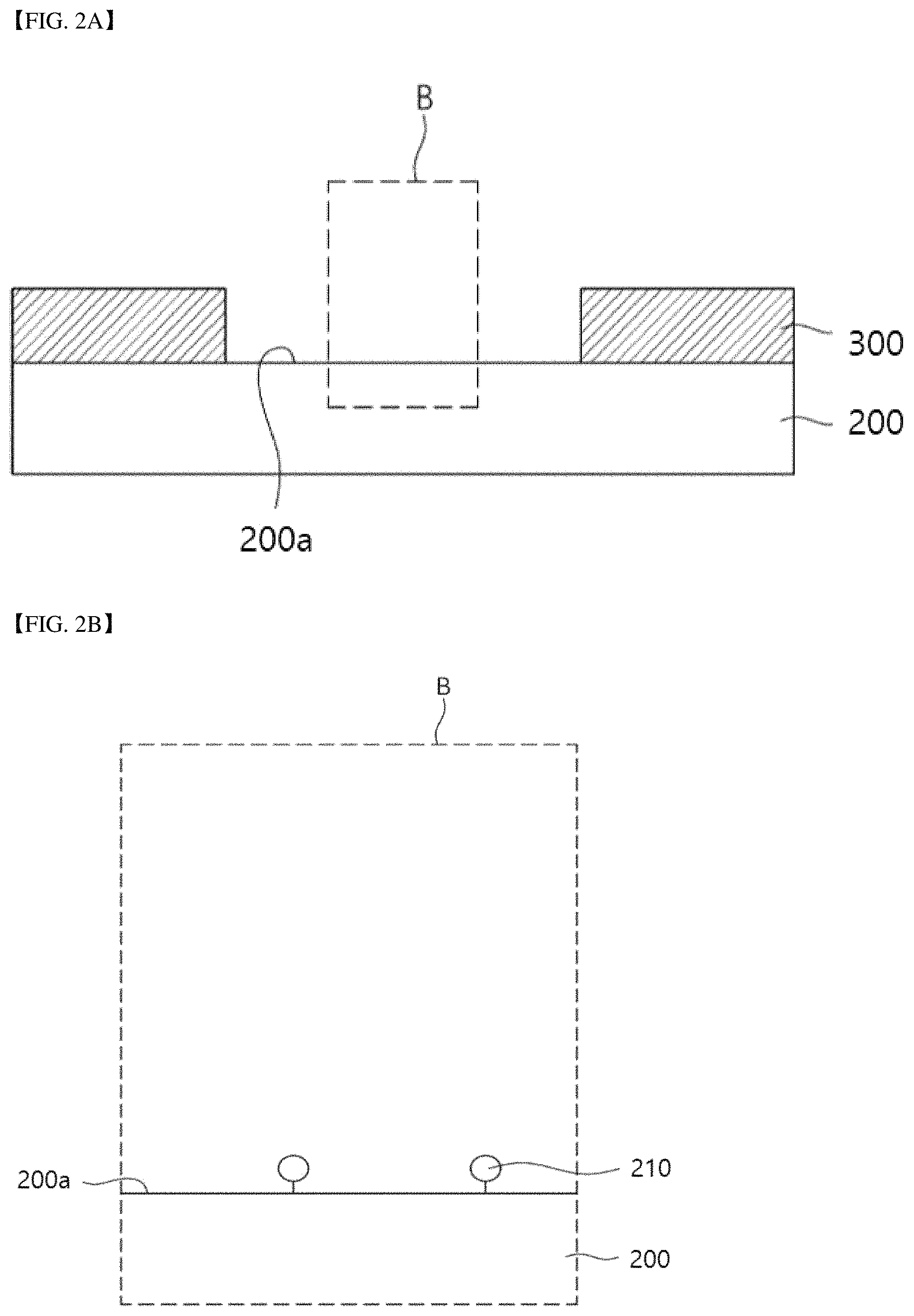
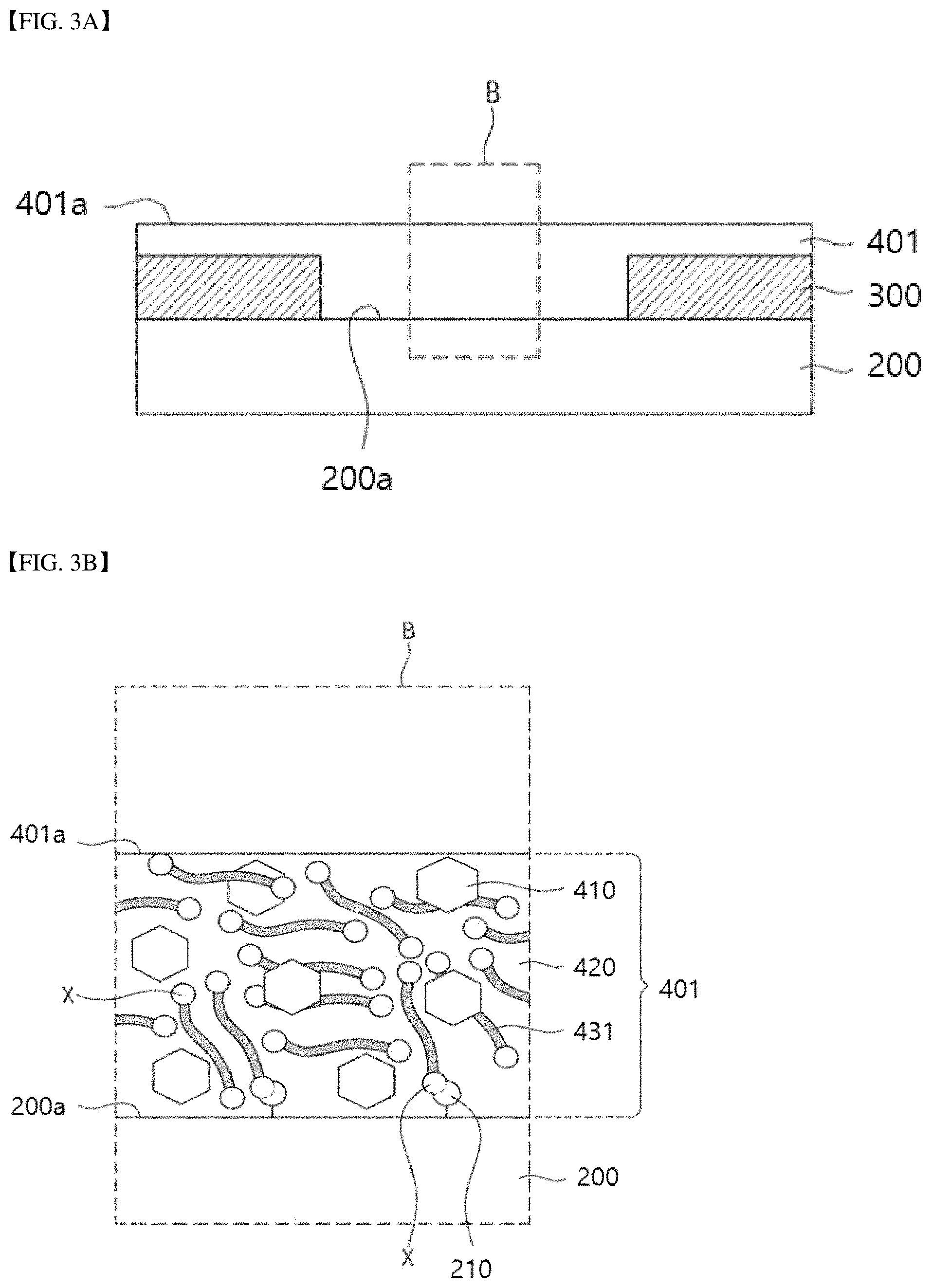
FIGS. 2A, 3A, 4A, 5A, and 6A are sectional views sequentially illustrating a process of fabricating an organic semiconductor device according to another embodiment of the present invention. In addition, FIGS. 2B, 3B, 4B, 5B, and 6B respectively illustrate B regions of FIGS. 2A, 3A, 4A, 5A, and 6A.
Referring to FIGS. 2A and 2B, source/drain patterns 300 may be formed on a substrate 200.
The substrate 200 may include an insulating material. For example, the substrate 200 may include an inorganic material such as silicon or glass. For example, the substrate 200 may include an organic material such as plastic or a polymer.
The substrate 200 may include functional groups 210 on an upper surface 200a thereof. The functional groups 210 of the substrate 200 may include at least one of a silanol group, a carboxyl group, a C1 to C30 alkoxycarbonyl group, a C3 to C30 aryloxycarbonyl group, and a hydroxyl group.
The source/drain patterns 300 may include a conductive material. For example, the source/drain patterns 300 may include at least one of a metal, doped polysilicon, a conductive polymer, and a conductive carbon material. Here, the conductive carbon material may include graphene. The source/drain patterns 300 may be formed to an upper surface 200a of the substrate 200.
In accordance with an embodiment, the functional groups 210 of the present invention, the substrate 200 may be covered by impurities (not shown).
The impurity may include a carbon-containing material, but the present invention is not limited thereto. To remove the impurity, a cleaning process may be further performed on the upper surface 200a of the substrate 200.
The cleaning process may be performed by oxygen plasma treatment or etching treatment using ozone and ultraviolet light.
By such a cleaning process, impurities may be removed and the functional groups 210 of the substrate 200 may be exposed.
Referring to FIGS. 3A and 3B, a preliminary organic semiconductor layer 401 may be formed on a substrate 200 to cover source/drain patterns 300.
The preliminary organic semiconductor layer 401 may include an organic semiconductor material 410, an organometallic precursor 431, and an organic solvent 420.
The organic semiconductor material 410 and the organometallic precursor 431 may be provided inside the organic solvent 420.
An organic semiconductor may mean an organic compound having semiconducting properties. For example, an organic compound having a n-conjugation structure may function as an organic semiconductor.
The .pi.-conjugation structure may be a structure wherein electrons are delocalized in p orbitals of an organic compound in which multiple bonds and single bonds are alternatingly disposed.
The organic compound may be composed of carbon atoms and hydrogen atoms. For example, the organic compound may further include a heteroatom. The heteroatom may include at least one of nitrogen, sulfur, and oxygen.
The organic semiconductor material 410 may be an organic compound having organic semiconducting properties, as described above. The organic semiconductor material 410 may include at least one of, for example, polyacetylene, polypyrrole, polyaniline, polythiophene (PTh), poly(p-phenylenevinylene (PPV)), and derivatives thereof.
The organic semiconductor material 410 may include at least one of, for example, polythiophene-based materials, polypyrrole-based materials, poly(p-phenylenevinylene)-based materials, polyanilines, polyacetylenes, polydiacetylenes, polycarbazoles, polyfuran-based materials, polyheteroaryls, nitrogen-containing aromatic compounds, condensed polycyclic aromatic compounds, aromatic amine derivatives, bis-carbazole derivatives, pyrazoline derivatives, stilbene-based compounds, hydrazine-based compounds, metal phthalocyanines, metal porphyrin-based materials, condensed rings, and organic pigments.
Here, the polythiophene-based materials may include poly-3-hexylthiophene or polybenzothiophene.
The poly(p-phenylenevinylene)-based materials may include poly(p-phenylenevinylene).
The polyfuran-based materials may include polyfuran or polybenzofuran.
A constituent unit of the polyheteroaryl-based materials may be a nitrogen-containing aromatic ring. The polyheteroaryl-based materials may include, for example, pyridine, quinoline, phenanthroline, oxazole, or oxadiazole.
The condensed polycyclic aromatic compounds may include anthracene, pyrene, naphthacene, pentacene, hexacene, or rubrene.
The nitrogen-containing aromatic compound may include furan, thiophene, benzothiophene, dibenzofuran, pyridine, quinoline, phenanthroline, oxazole, or oxadiazole.
The aromatic amine derivatives may include 4,4'-bis(N-(3-methylphenyl)-N-phenylamino)biphenyl.
The bis-carbazole derivatives may include bis(N-allylcarbazole) or bis(N-alkylcarbazole).
The metal phthalocyanines may include copper phthalocyanine.
The metal porphyrins may include copper porphyrin.
The condensed rings may include a distyrylbenzene derivative, an aminostyryl derivative, an aromatic acetylene derivative, naphthalene-1,4,5,8-tetracarboxylic acid diimide, or perylene-3,4,9,10-tetracarboxylic acid diimide.
The organic pigments may include tetracarboxylic acid diimides, merocyanine, phenoxazine, or rhodamine.
However, the organic semiconductor material 410 may include various materials without being limited to the aforementioned materials.
The organometallic precursor may be represented by Formula 1 below:
##STR00005##
wherein M1 and M2 each independently include at least one of Sc, Ti, V, Cr, Mn, Fe, Co, Ni, Si, Cu, Zn, Pd, Ag, Au, Hg, Pt, Ta, Mo, Zr, Ta, Mg, Sn, Ge, Y, Nb, Tc, Ru, Rh, Lu, Hf, W, Re, Os, Ir, Lr, Rf, Db, Sg, Bh, Hs, Mt, Ds, Rg, and Uub,
Y is one of a substituted or unsubstituted C1 to C30 alkyl group, a C3 to C30 cycloalkyl group, a C3 to C30 heterocyclic group, a C2 to C30 alkenyl group, a C3 to C30 cycloalkenyl group, a C2 to C30 alkynyl group, a C1 to C30 alkoxy group, a C1 to C30 alkylthio group, a C3 to C30 arylether group, a C3 to C30 arylthioether group, a C3 to C30 aryl group, a C3 to C30 heteroaryl group, a halogen atom, a cyano group, a formyl group, a C1 to C30 alkylcarbonyl group, a C3 to C30 arylcarbonyl group, a carboxyl group, a C1 to C30 alkoxycarbonyl group, a C3 to C30 aryloxycarbonyl group, a C1 to C30 alkylcarbonyloxy group, a C1 to C30 arylcarbonyloxy group, a carbamoyl group, an amino group, and a silyl group, and
X1 and X2 are each independently one selected from among a hydrogen atom, a substituted or unsubstituted C1 to C30 alkyl group, a C3 to C30 cycloalkyl group, a C3 to C30 heterocyclic group, a C2 to C30 alkenyl group, a C3 to C30 cycloalkenyl group, a C2 to C30 alkynyl group, a C1 to C30 alkoxy group, a C1 to C30 alkylthio group, a C3 to C30 arylether group, a C3 to C30 arylthioether group, a C3 to C30 aryl group, a C3 to C30 heteroaryl group, a halogen atom, a cyano group, a formyl group, a C1 to C30 alkylcarbonyl group, a C3 to C30 arylcarbonyl group, a carboxyl group, a C1 to C30 alkoxycarbonyl group, a C3 to C30 aryloxycarbonyl group, a C1 to C30 alkylcarbonyloxy group, a C1 to C30 arylcarbonyloxy group, a carbamoyl group, an amino group, and a hydroxyl group, wherein the substituted alkyl group includes an alkyl group substituted with a halogen element.
In accordance with an embodiment of the present invention, Formula 1, at least one of X.sub.1 and X.sub.2 may be a C1 to C30 alkoxy group, a C1 to C30 alkylthio group, a C3 to C30 arylether group, a C3 to C30 arylthioether group, a C3 to C30 aryl group, a C3 to C30 heteroaryl group, a halogen atom, a cyano group, a formyl group, a C1 to C30 alkylcarbonyl group, a C3 to C30 arylcarbonyl group, a carboxyl group, a C1 to C30 alkoxycarbonyl group, a C3 to C30 aryloxycarbonyl group, a C1 to C30 alkylcarbonyloxy group, a C1 to C30 arylcarbonyloxy group, a carbamoyl group, an amino group, and a hydroxyl group.
In addition, in accordance with an embodiment of the present invention, in Formula 1, at least one of X.sub.1 and at least one of X2 may be each independently a C1 to C30 alkoxy group, a C1 to C30 alkylthio group, a C3 to C30 arylether group, a C3 to C30 arylthioether group, a C3 to C30 aryl group, a C3 to C30 heteroaryl group, a halogen atom, a cyano group, a formyl group, a C1 to C30 alkylcarbonyl group, a C3 to C30 arylcarbonyl group, a carboxyl group, a C1 to C30 alkoxycarbonyl group, a C3 to C30 aryloxycarbonyl group, a C1 to C30 alkylcarbonyloxy group, a C1 to C30 arylcarbonyloxy group, a carbamoyl group, an amino group, and a hydroxyl group.
The organometallic precursor may include the first reactive groups X bonded with an inorganic element. The inorganic element may be denoted as M.sub.1 and M.sub.2 in Formula 1. The first reactive group (X) may be at least one of groups denoted as X.sub.1 and X.sub.2 in Formula 1. The first reactive group (X) may include at least one of a C1 to C30 alkoxy group, a C1 to C30 alkylthio group, a C3 to C30 arylether group, a C3 to C30 arylthioether group, a C3 to C30 aryl group, a C3 to C30 heteroaryl group, a halogen atom, a cyano group, a formyl group, a C1 to C30 alkylcarbonyl group, a C3 to C30 arylcarbonyl group, a carboxyl group, a C1 to C30 alkoxycarbonyl group, a C3 to C30 aryloxycarbonyl group, a C1 to C30 alkylcarbonyloxy group, a C1 to C30 arylcarbonyloxy group, a carbamoyl group, an amino group, and a hydroxyl group.
The organic solvent 420 may include at least one of chloroform, dichloromethane, acetone, pyridine, tetrahydrofuran, chlorobenzene, dichlorobenzene, xylene, trichlorobenzene, toluene, and a mixture thereof.
In accordance with an embodiment of the present invention, an organic semiconductor solution may be prepared by mixing the organic semiconductor material 410, the organic solvent 420, and the organometallic precursor 431.
The organic semiconductor solution may be coated on the substrate 200, thereby forming the preliminary organic semiconductor layer 401.
For example, the organic semiconductor solution may be coated by a spin coating method, a spray coating method, an inkjet printing method, a dip coating method, a drop casting method, or a bar coating method.
As shown in FIG. 3A, the preliminary organic semiconductor layer 401 may cover the source/drain patterns 300 and the substrate 200.
In addition, as shown in FIG. 3B, first reactive groups X of the organometallic precursor 431 may react with functional groups 210 of the substrate 200.
Reaction between the first reactive groups X of the organometallic precursor 431 and the functional groups 210 of the substrate 200 may include condensation reaction.
Accordingly, a chemical bond (e.g., covalent bond) may be formed between the preliminary organic semiconductor layer 401 and the substrate 200.
For example, the first reactive groups X of the organometallic precursor 431 and the functional groups 210 of the substrate 200 may be silanol groups.
In this case, a siloxane bond may be formed between the preliminary organic semiconductor layer 401 and the substrate 200.
When impurities (not shown) are provided on the functional groups 210, it may be difficult to react the organometallic precursor 431 with the functional groups 210 of the substrate 200.
In this case, binding force between the substrate 200 and the preliminary organic semiconductor layer 401 may be reduced.
In accordance with an embodiment of the present invention of the present invention, impurities are removed by a cleaning process of FIGS. 3A and 3B, thereby increasing binding force between the substrate 200 and the preliminary organic semiconductor layer 401.
The first reactive groups X of the organometallic precursor 431 may function as a dopant of the organic semiconductor material 410.
In the preliminary organic semiconductor layer 401, the content of the first reactive groups X of the organometallic precursor 431 may be higher than that of the organic semiconductor material 410.
The preliminary organic semiconductor layer 401 may exhibit conductivity. The organometallic precursor 431 may include a plurality of organometallic precursors 431. These organometallic precursors 431 may be dispersed in the preliminary organic semiconductor layer 401.
The first reactive groups X of the organometallic precursors 431 may be provided on an upper surface 401a of the preliminary organic semiconductor layer 401 and inside the preliminary organic semiconductor layer 401.
Referring to FIGS. 3A, 3B, 4A, and 4B in sequence, the preliminary organic semiconductor layer 401 may be annealed to form an organic semiconductor layer 400.
The annealing of the preliminary organic semiconductor layer 401 may be performed by heat-treating the same at 50.degree. C. to 300.degree. C.
When the preliminary organic semiconductor layer 401 is heat-treated at a temperature higher than 300.degree. C., the organic semiconductor layer 400 may be damaged.
The preliminary organic semiconductor layer 401 may be gelated by the annealing process. During the annealing process, the organic solvent 420 may be removed.
In the annealing process, the first reactive groups X of the organometallic precursors 431 may react with each other.
The reaction between the organometallic precursors 431 may include hydrolysis or condensation reaction.
Accordingly, the organometallic precursors 431 may be bonded (e.g., cross-linked) to one another, thereby forming a lattice structure 430 of FIG. 4B.
The organic semiconductor layer 400 may include the lattice structure 430 and the organic semiconductor material 410.
The lattice structure 430 may have a ladder-like structure, but the present invention is not limited thereto.
The lattice structure 430 may be bonded to the substrate 200.
End portions of the lattice structure 430 may be exposed to the upper surfaces 400a of the organic semiconductor layer 400 and may include the first reactive groups X.
The first reactive groups X of the lattice structure 430 may be derived from the first reactive groups X of the organometallic precursors 431 of FIG. 3B.
In the present specification, the first reactive groups X of the organic semiconductor layer 400 may mean the first reactive groups X of the lattice structure 430.
Due to the lattice structure 430, chemical resistance and durability of the organic semiconductor layer 400 may be improved.
The organic semiconductor material 410 may be dispersed in the lattice structure 430, and the organic semiconductor material 410 may not chemically bond to the lattice structure 430.
The organic semiconductor material 410 may physically contact the lattice structure 430.
In accordance with embodiments of the present invention, the first reactive groups X may be bonded to each other to form the lattice structure 430.
The content of the first reactive groups X in the organic semiconductor layer 400 may be lower than that of the first reactive groups X in the preliminary organic semiconductor layer 401.
For example, the first reactive groups X may be provided on the upper surfaces 400a of the organic semiconductor layer 400, but not in the organic semiconductor layer 400.
When the functional groups 210 of the substrate 200 (see FIG. 2B) remain, the functional groups 210 may function as an electron/hole trap. In accordance with embodiments of the present invention, the functional groups 210 of the substrate 200 are removed, thereby improving electrical characteristics of the organic semiconductor layer 400.
Referring to FIGS. 5A and 5B, a self-assembling precursor 510 may be coated on an organic semiconductor layer 400, thereby forming a self-assembled monolayer 500.
Here, the self-assembling precursor 510 may be represented by Formula 2 below:
##STR00006##
wherein A includes one of --NH2, --CH3, --SH, --COOH, --CF3, and a halogen element, the halogen element including one of F, Cl, Br, and I,
R is one selected from among a substituted or unsubstituted C1 to C30 alkyl group, a C3 to C30 cycloalkyl group, a C3 to C30 heterocyclic group, a C2 to C30 alkenyl group, a C3 to C30 cycloalkenyl group, a C2 to C30 alkynyl group, a C1 to C30 alkoxy group, a C1 to C30 alkylthio group, a C3 to C30 arylether group, a C3 to C30 arylthioether group, a substituted or unsubstituted C3 to C30 aryl group, a C3 to C30 heteroaryl group, halogen atom, a cyano group, a formyl group, a C1 to C30 alkylcarbonyl group, a C3 to C30 arylcarbonyl group, a carboxyl group, a C1 to C30 alkoxycarbonyl group, a C3 to C30 aryloxycarbonyl group, a C1 to C30 alkylcarbonyloxy group, a C1 to C30 arylcarbonyloxy group, a carbamoyl group, a substituted or unsubstituted thiophene, an amino group, and a hydroxyl group, the substituted alkyl group including an alkyl group substituted with a halogen element,
n is an integer of 0 to 30,
M3 is one of Sc, Ti, V, Cr, Mn, Fe, Co, Ni, Si, Cu, Zn, Pd, Ag, Au, Hg, Pt, Ta, Mo, Zr, Ta, Mg, Sn, Ge, Y, Nb, Tc, Ru, Rh, Lu, Hf, W, Re, Os, Jr, Lr, Rf, Db, Sg, Bh, Hs, Mt, Ds, Rg, and Uub, and
X3 are each independently one selected from among a hydrogen atom, a substituted or unsubstituted C1 to C30 alkyl group, a C3 to C30 cycloalkyl group, a C3 to C30 heterocyclic group, a C2 to C30 alkenyl group, a C3 to C30 cycloalkenyl group, a C2 to C30 alkynyl group, a C1 to C30 alkoxy group, a C1 to C30 alkylthio group, a C3 to C30 arylether group, a C3 to C30 arylthioether group, a C3 to C30 aryl group, a C3 to C30 heteroaryl group, a halogen atom, a cyano group, a formyl group, a C1 to C30 alkylcarbonyl group, a C3 to C30 arylcarbonyl group, a carboxyl group, a C1 to C30 alkoxycarbonyl group, a C3 to C30 aryloxycarbonyl group, a C1 to C30 alkylcarbonyloxy group, a C1 to C30 arylcarbonyloxy group, a carbamoyl group, an amino group, and a hydroxyl group, the substituted alkyl group of X3 including an alkyl group substituted with a halogen element.
In accordance with an embodiment of the present invention, Formula 2, at least one of X.sub.3 may be one selected from among a C1 to C30 alkoxy group, a C1 to C30 alkylthio group, a C3 to C30 arylether group, a C3 to C30 arylthioether group, a C3 to C30 aryl group, a C3 to C30 heteroaryl group, a halogen atom, a cyano group, a formyl group, a C1 to C30 alkylcarbonyl group, a C3 to C30 arylcarbonyl group, a carboxyl group, a C1 to C30 alkoxycarbonyl group, a C3 to C30 aryloxycarbonyl group, a C1 to C30 alkylcarbonyloxy group, a C1 to C30 arylcarbonyloxy group, a carbamoyl group, an amino group, and a hydroxyl group.
The self-assembling precursor 510 may be selected from the group consisting of, for example, octyltrichlorosilane (OTS), octyltrimethoxysilane (OTMS), octyltriethoxysilane (OTES), hexamethyldisilazane (HMDS), octadecyltrichlorosilane (ODTS), octadecyltrimethoxysilane (OTMS), octadecyltriethoxysilane (OTE), (3-aminopropyl)trichlorosilane, (3-aminopropyl)trimethoxysilane (APTMS), (3-aminopropyl)triethoxysilane (APTES), fluoroalkyl trichlorosilane (FTS), perfluorodecyltrichlorosilane (PFTS), perfluorodecyltrimethoxysilane (PFMS), perfluorodecyltriethoxysilane (PFES), mercaptopropyltrichlorosilane (MPTCS), mercaptopropyltrimethoxysilane (MPTMS), mercaptopropyltriethoxysilane (MPTES), heptadecafluoro-1,1,2,2 tetrahydrodecyl)trichlorosilane (FDTS), heptadecafluoro-1,1,2,2-tetrahydrodecyl)trimethoxysilane; (FDMS), heptadecafluoro-1,1,2,2-tetrahydrodecyl)triethoxysilane (FDES), 1H,1H,2H,2H-perfluorodecyltrichlorosilane (FOTS), 1H,1H,2H,2H-perfluorodecyltrimethoxysilane (FOMS), 1H,1H,2H,2H-perfluorodecyltriethoxysilane (FOES), dichlorodimethylsilane (DDMS), trichloromethylsilane (TCMS), 3-aminopropyl(triethoxysilane) (APS), trimethoxysilylpropyldiethylenetriamine (DETA), N-(2-aminoethyl)-3-aminopropyltrimethoxysilane (EDA), and combinations thereof.
As shown in FIG. 5B, the self-assembling precursor 510 may include second reactive groups X.sub.3 and functional groups A. The second reactive groups X.sub.3 of the self-assembling precursor 510 may be at least one of groups represented by X.sub.3 in Formula 2.
The second reactive groups X.sub.3 may be selected from among a C1 to C30 alkoxy group, a C1 to C30 alkylthio group, a C3 to C30 arylether group, a C3 to C30 arylthioether group, a C3 to C30 aryl group, a C3 to C30 heteroaryl group, a halogen atom, a cyano group, a formyl group, a C1 to C30 alkylcarbonyl group, a C3 to C30 arylcarbonyl group, a carboxyl group, a C1 to C30 alkoxycarbonyl group, a C3 to C30 aryloxycarbonyl group, a C1 to C30 alkylcarbonyloxy group, a C1 to C30 arylcarbonyloxy group, a carbamoyl group, an amino group, and a hydroxyl group.
The functional groups A of the self-assembling precursor 510 may be represented as A in Formula 2.
One of the second reactive groups X.sub.3 of the self-assembling precursor 510 may react with one of the first reactive groups X of the organic semiconductor layer 400.
Accordingly, the self-assembled monolayer 500 may be chemically bonded with the organic semiconductor layer 400.
The chemical bond between the self-assembled monolayer 500 and the organic semiconductor layer 400 may include a covalent bond (e.g., silanol bond).
The functional groups A of the self-assembling precursor 510 may not react with the first reactive groups X of the organic semiconductor layer 400.
Accordingly, the self-assembled monolayer 500 may have the functional groups A, and the functional groups A of the self-assembled monolayer 500 may be derived from the functional groups A of the self-assembling precursor 510.
The functional groups A of the self-assembled monolayer 500 may be provided on an upper surface 500a of the self-assembled monolayer 500.
The upper surface 500a of the self-assembled monolayer 500 may be opposite to the organic semiconductor layer 400.
The functional groups A of the self-assembled monolayer 500 may be different from the first reactive groups X of the organic semiconductor layer 400.
Affinity of the self-assembled monolayer 500 for a material may be different from affinity of the organic semiconductor layer 400 for the material.
Here, the affinity of the self-assembled monolayer 500 may mean affinity of the functional groups A of the self-assembled monolayer 500, and the affinity of the organic semiconductor layer 400 may mean affinity of the first reactive groups X of the organic semiconductor layer 400.
In the present specification, affinity may be used as a meaning including the ability to react with a substance or the ability to interact with a substance.
Referring to FIGS. 6A and 6B, an insulating layer 600 may be formed on an upper surface 500a of a self-assembled monolayer 500.
The insulating layer 600 may include an inorganic insulating material such as silicon oxide.
For example, the insulating layer 600 may include organic insulating material. The organic insulating material may include at least one of polyvinyl alcohol (PVA), polyvinyl phenol (PVP), polymethyl methacrylate (PMMA), and polyimide (PI).
The insulating layer 600 may have functional groups.
Binding force between the insulating layer 600 and the self-assembled monolayer 500 may be determined by affinity between the functional groups of the insulating layer 600 and the self-assembled monolayer 500.
The affinity of the self-assembled monolayer 500 to the insulating layer 600 may have greater than the affinity of the organic semiconductor layer 400 to the insulating layer 600.
When the binding force between the insulating layer 600 and the self-assembled monolayer 500 increases, durability of an organic semiconductor device 1 may increase.
The insulating layer 600 may be easily formed on the upper surface 500a of the self-assembled monolayer 500.
In accordance with embodiments of the present invention, electrical characteristics may be further improved according to the characteristics of the self-assembled monolayer 500 imparted due to the self-assembled monolayer 500 formed on the organic semiconductor layer 400.
A gate pattern 700 may be formed on the insulating layer 600, and the gate pattern 700 may include a conductive material.
For example, the gate pattern 700 may include at least one of a metal, doped polysilicon, a conductive polymer, and a conductive carbon material.
According to the aforementioned fabrication steps, the organic semiconductor device 1 according to another embodiment of the present invention may be fabricated.
The organic semiconductor device according to another embodiment of the present invention may include the organic semiconductor compound according to an embodiment of the present invention as a semiconductor layer.
The organic semiconductor device may be a sensor for analyzing a sample containing a biomaterial or chemical in a liquid, solid, or gaseous state.
In addition, the organic semiconductor device according to another embodiment of the present invention may be an organic solar cell including the organic semiconductor compound according to an embodiment of the present invention as an active layer.
In addition, the organic semiconductor device according to another embodiment of the present invention may be an organic light-emitting diode including the organic semiconductor compound according to an embodiment of the present invention as a light emitting layer.
Meanwhile, embodiments of the present invention disclosed in the present specification and drawings have been only provided to help understanding of the present invention and the scope of the present invention is not limited to the embodiments. It will be apparent to those skilled in the art that various modifications can be made to the above-described exemplary embodiments of the present invention without departing from the spirit or scope of the invention.
* * * * *
C00001
C00002
C00003
C00004
C00005
C00006
C00007
C00008
D00000
D00001
D00002
D00003
D00004

D00005

D00006

XML
uspto.report is an independent third-party trademark research tool that is not affiliated, endorsed, or sponsored by the United States Patent and Trademark Office (USPTO) or any other governmental organization. The information provided by uspto.report is based on publicly available data at the time of writing and is intended for informational purposes only.
While we strive to provide accurate and up-to-date information, we do not guarantee the accuracy, completeness, reliability, or suitability of the information displayed on this site. The use of this site is at your own risk. Any reliance you place on such information is therefore strictly at your own risk.
All official trademark data, including owner information, should be verified by visiting the official USPTO website at www.uspto.gov. This site is not intended to replace professional legal advice and should not be used as a substitute for consulting with a legal professional who is knowledgeable about trademark law.