Apparatus and method to share host system RAM with mass storage memory RAM
Luukkainen , et al. April 20, 2
U.S. patent number 10,983,697 [Application Number 15/989,695] was granted by the patent office on 2021-04-20 for apparatus and method to share host system ram with mass storage memory ram. This patent grant is currently assigned to Memory Technologies LLC. The grantee listed for this patent is Memory Technologies LLC. Invention is credited to Jani Hyvonen, Olli Luukkainen, Kimmo Mylly.
| United States Patent | 10,983,697 |
| Luukkainen , et al. | April 20, 2021 |
Apparatus and method to share host system RAM with mass storage memory RAM
Abstract
A method includes, in one non-limiting embodiment, sending a request from a mass memory storage device to a host device, the request being one to allocate memory in the host device; writing data from the mass memory storage device to allocated memory of the host device; and subsequently reading the data from the allocated memory to the mass memory storage device. The memory may be embodied as flash memory, and the data may be related to a file system stored in the flash memory. The method enables the mass memory storage device to extend its internal volatile RAM to include RAM of the host device, enabling the internal RAM to be powered off while preserving data and context stored in the internal RAM.
| Inventors: | Luukkainen; Olli (Salo, FI), Mylly; Kimmo (Ylojarvi, FI), Hyvonen; Jani (Tampere, FI) | ||||||||||
|---|---|---|---|---|---|---|---|---|---|---|---|
| Applicant: |
|
||||||||||
| Assignee: | Memory Technologies LLC
(Kirkland, WA) |
||||||||||
| Family ID: | 1000005500544 | ||||||||||
| Appl. No.: | 15/989,695 | ||||||||||
| Filed: | May 25, 2018 |
Prior Publication Data
| Document Identifier | Publication Date | |
|---|---|---|
| US 20180364909 A1 | Dec 20, 2018 | |
Related U.S. Patent Documents
| Application Number | Filing Date | Patent Number | Issue Date | ||
|---|---|---|---|---|---|
| 15335688 | Oct 27, 2016 | 9983800 | |||
| 14945757 | Nov 19, 2015 | ||||
| 14520030 | Dec 8, 2015 | 9208078 | |||
| 12455763 | Oct 28, 2014 | 8874824 | |||
| Current U.S. Class: | 1/1 |
| Current CPC Class: | G06F 3/0631 (20130101); G06F 12/0223 (20130101); G06F 3/0655 (20130101); G06F 3/061 (20130101); G06F 12/0246 (20130101); G06F 12/0638 (20130101); G06F 3/0679 (20130101); G06F 2212/7207 (20130101); G06F 2212/7203 (20130101); Y02D 10/00 (20180101); G06F 2212/7202 (20130101); G06F 2212/205 (20130101); G06F 2212/171 (20130101) |
| Current International Class: | G06F 13/00 (20060101); G06F 3/06 (20060101); G06F 12/06 (20060101); G06F 13/28 (20060101); G06F 12/02 (20060101) |
References Cited [Referenced By]
U.S. Patent Documents
| 5586291 | December 1996 | Lasker et al. |
| 5701516 | December 1997 | Cheng et al. |
| 5710931 | January 1998 | Nakamura et al. |
| 5781753 | July 1998 | McFarland et al. |
| 5802069 | September 1998 | Coulson |
| 5805882 | September 1998 | Cooper et al. |
| 5809340 | September 1998 | Bertone et al. |
| 5822553 | October 1998 | Gifford et al. |
| 5924097 | July 1999 | Hill et al. |
| 5933626 | August 1999 | Mahalingaiah |
| 6067300 | May 2000 | Baumert et al. |
| 6115785 | September 2000 | Estakhri et al. |
| 6122196 | September 2000 | Tanaka |
| 6173425 | January 2001 | Knaack et al. |
| 6226710 | May 2001 | Melchior |
| 6373768 | April 2002 | Woo et al. |
| 6480936 | November 2002 | Ban et al. |
| 6513094 | January 2003 | Magro |
| 6522586 | February 2003 | Wong |
| 6526472 | February 2003 | Suzuki |
| 6609182 | August 2003 | Pedrizetti et al. |
| 6665747 | December 2003 | Nazari |
| 6732221 | May 2004 | Ban |
| 6785764 | August 2004 | Roohparvar |
| 6842829 | January 2005 | Nichols et al. |
| 6901298 | May 2005 | Govindaraj et al. |
| 7047368 | May 2006 | Vantalon et al. |
| 7136963 | November 2006 | Ogawa et al. |
| 7181574 | February 2007 | Lele |
| 7233538 | June 2007 | Wu et al. |
| 7321958 | January 2008 | Hofstee et al. |
| 7395176 | July 2008 | Chung et al. |
| 7412559 | August 2008 | Stockdale et al. |
| 7450456 | November 2008 | Jain et al. |
| 7480749 | January 2009 | Danilak |
| 7492368 | February 2009 | Nordquist et al. |
| 7571295 | August 2009 | Sakarda et al. |
| 7644938 | January 2010 | Yamada |
| 7697311 | April 2010 | Fukuda et al. |
| 7730248 | June 2010 | Goss et al. |
| 7760569 | July 2010 | Ruf et al. |
| 7783845 | August 2010 | Bennett et al. |
| 7809962 | October 2010 | Chang et al. |
| 7889544 | February 2011 | Chow et al. |
| 8094500 | January 2012 | Paley et al. |
| 8180975 | May 2012 | Moscibroda et al. |
| 8190803 | May 2012 | Hobson et al. |
| 8218137 | July 2012 | Noh et al. |
| 8307180 | November 2012 | Hyvonen et al. |
| 8321713 | November 2012 | Nobunaga |
| 8327123 | December 2012 | Juffa et al. |
| 8514621 | August 2013 | Choi et al. |
| 8527693 | September 2013 | Flynn et al. |
| 8639874 | January 2014 | Maule et al. |
| 8656045 | February 2014 | Wallace et al. |
| 8826051 | September 2014 | Wakrat et al. |
| 8879346 | November 2014 | Kam et al. |
| 8935302 | January 2015 | Flynn et al. |
| 9003159 | April 2015 | Deshkar et al. |
| 9063724 | June 2015 | Smith et al. |
| 9069551 | June 2015 | Iarovici et al. |
| 9128718 | September 2015 | Lachwani et al. |
| 9141394 | September 2015 | Sakarda |
| 9424182 | August 2016 | Fisher et al. |
| 9645758 | May 2017 | Peterson et al. |
| 9667425 | May 2017 | Goss et al. |
| 9710377 | July 2017 | Kuzmin et al. |
| 9727454 | August 2017 | Kuzmin et al. |
| 9829951 | November 2017 | Kumar et al. |
| 9841911 | December 2017 | Yu et al. |
| 9870327 | January 2018 | Chen et al. |
| 9941007 | April 2018 | Peddle et al. |
| 9952977 | April 2018 | Heinrich et al. |
| 10095613 | October 2018 | Jo et al. |
| 2002/0000931 | January 2002 | Petronic et al. |
| 2002/0087817 | July 2002 | Tomaiuolo et al. |
| 2002/0093913 | July 2002 | Brown et al. |
| 2002/0108014 | August 2002 | Lasser |
| 2003/0028737 | February 2003 | Kaiya et al. |
| 2003/0137860 | July 2003 | Khatri et al. |
| 2004/0010671 | January 2004 | Sampsa et al. |
| 2004/0049692 | March 2004 | Okamoto |
| 2004/0203670 | October 2004 | King et al. |
| 2004/0221124 | November 2004 | Beckert et al. |
| 2004/0230317 | November 2004 | Kumar et al. |
| 2005/0010738 | January 2005 | Stockdale et al. |
| 2005/0071570 | March 2005 | Takasugl et al. |
| 2005/0097280 | May 2005 | Hofstee et al. |
| 2005/0138318 | June 2005 | Ash et al. |
| 2005/0204113 | September 2005 | Harper et al. |
| 2006/0041888 | February 2006 | Radulescu et al. |
| 2006/0069899 | March 2006 | Schoinas et al. |
| 2006/0075147 | April 2006 | Schoinas et al. |
| 2006/0075395 | April 2006 | Lee et al. |
| 2006/0119602 | June 2006 | Fisher et al. |
| 2006/0120235 | June 2006 | Jensen |
| 2006/0129722 | June 2006 | Campbell |
| 2006/0174056 | August 2006 | Lambert et al. |
| 2006/0179212 | August 2006 | Kim et al. |
| 2006/0184758 | August 2006 | Satori et al. |
| 2006/0224789 | October 2006 | Cho et al. |
| 2006/0280077 | December 2006 | Suwa |
| 2007/0088867 | April 2007 | Cho et al. |
| 2007/0136523 | June 2007 | Bonella et al. |
| 2007/0147115 | June 2007 | Lin et al. |
| 2007/0207854 | September 2007 | Wolf et al. |
| 2007/0226795 | September 2007 | Conti et al. |
| 2007/0234006 | October 2007 | Radulescu et al. |
| 2007/0283078 | December 2007 | Li et al. |
| 2008/0080688 | April 2008 | Burgan et al. |
| 2008/0104291 | May 2008 | Hinchey |
| 2008/0126857 | May 2008 | Basham et al. |
| 2008/0127131 | May 2008 | Gao et al. |
| 2008/0162792 | July 2008 | Wu et al. |
| 2008/0183954 | July 2008 | Lee et al. |
| 2008/0189485 | August 2008 | Jung et al. |
| 2008/0228984 | September 2008 | Yu et al. |
| 2008/0235477 | September 2008 | Rawson |
| 2008/0244173 | October 2008 | Takai |
| 2008/0281944 | November 2008 | Vorne et al. |
| 2008/0282030 | November 2008 | Kalwitz et al. |
| 2008/0320211 | December 2008 | Kinoshita |
| 2009/0106503 | April 2009 | Lee et al. |
| 2009/0157950 | June 2009 | Selinger |
| 2009/0164705 | June 2009 | Gorobets |
| 2009/0182940 | July 2009 | Matsuda et al. |
| 2009/0182962 | July 2009 | Khmelnitsky et al. |
| 2009/0198871 | August 2009 | Tzeng |
| 2009/0198872 | August 2009 | Tzeng |
| 2009/0210615 | August 2009 | Struk et al. |
| 2009/0216937 | August 2009 | Yasufuku |
| 2009/0222629 | September 2009 | Yano et al. |
| 2009/0292861 | November 2009 | Kanevsky |
| 2009/0307377 | December 2009 | Anderson et al. |
| 2009/0307544 | December 2009 | Kim et al. |
| 2009/0313420 | December 2009 | Wiesz et al. |
| 2009/0327584 | December 2009 | Tetrick et al. |
| 2010/0005281 | January 2010 | Buchmann et al. |
| 2010/0030961 | February 2010 | Ma et al. |
| 2010/0037012 | February 2010 | Yano et al. |
| 2010/0082905 | April 2010 | Wilkerson et al. |
| 2010/0100648 | April 2010 | Madukkarumukumana et al. |
| 2010/0106886 | April 2010 | Marcu et al. |
| 2010/0106901 | April 2010 | Higeta et al. |
| 2010/0115193 | May 2010 | Manus et al. |
| 2010/0161882 | June 2010 | Stern et al. |
| 2010/0169558 | July 2010 | Honda et al. |
| 2010/0169604 | July 2010 | Trika et al. |
| 2010/0172180 | July 2010 | Paley et al. |
| 2010/0250836 | September 2010 | Sokolov et al. |
| 2010/0268928 | October 2010 | Wang et al. |
| 2010/0293420 | November 2010 | Kapil et al. |
| 2010/0306503 | December 2010 | Henry et al. |
| 2010/0312947 | December 2010 | Luukkainen et al. |
| 2011/0029808 | February 2011 | Moshayedi |
| 2011/0082967 | April 2011 | Deshkar et al. |
| 2011/0087804 | April 2011 | Okaue et al. |
| 2011/0099326 | April 2011 | Jung et al. |
| 2011/0145537 | June 2011 | Feldman et al. |
| 2011/0208914 | August 2011 | Winokur et al. |
| 2011/0264860 | October 2011 | Hooker et al. |
| 2011/0296088 | December 2011 | Duzly et al. |
| 2012/0023303 | January 2012 | Russo et al. |
| 2012/0079171 | March 2012 | Ju et al. |
| 2012/0102268 | April 2012 | Smith et al. |
| 2012/0131263 | May 2012 | Yeh |
| 2012/0131269 | May 2012 | Fisher et al. |
| 2012/0151118 | June 2012 | Flynn et al. |
| 2012/0210326 | August 2012 | Torr et al. |
| 2012/0221875 | August 2012 | Bak et al. |
| 2012/0239990 | September 2012 | Mataya et al. |
| 2012/0324299 | December 2012 | Moshayedi |
| 2013/0007348 | January 2013 | Fai et al. |
| 2013/0138840 | May 2013 | Kegel et al. |
| 2013/0145055 | June 2013 | Kegel et al. |
| 2013/0282957 | October 2013 | Mylly |
| 2013/0332691 | December 2013 | Hyvonen et al. |
| 2013/0339635 | December 2013 | Amit et al. |
| 2013/0346668 | December 2013 | Floman et al. |
| 2013/0346685 | December 2013 | Hampel et al. |
| 2014/0059273 | February 2014 | Fujimoto et al. |
| 2014/0068140 | March 2014 | Mylly |
| 2014/0188719 | July 2014 | Poornachandran et al. |
| 2014/0304475 | October 2014 | Ramanujan et al. |
| 2015/0039819 | February 2015 | Luukkainen et al. |
| 2015/0134871 | May 2015 | Benisty et al. |
| 2015/0160863 | June 2015 | Mylly |
| 2015/0269094 | September 2015 | Hyvonen et al. |
| 2016/0062659 | March 2016 | Floman et al. |
| 2016/0077963 | March 2016 | Luukkainen et al. |
| 2016/0246546 | August 2016 | Mylly |
| 2016/0306588 | October 2016 | Li et al. |
| 2016/0357436 | December 2016 | Hyvonen et al. |
| 2017/0038975 | February 2017 | Mylly et al. |
| 2017/0046067 | February 2017 | Luukkainen et al. |
| 2018/0130506 | May 2018 | Kang et al. |
| 2018/0137058 | May 2018 | Heo et al. |
| 2019/0034122 | January 2019 | Mylly |
| 2020/0089403 | March 2020 | Hyvonen et al. |
| 2020/0218448 | July 2020 | Hyvonen et al. |
| 2005200855 | Sep 2004 | AU | |||
| 1517886 | Aug 2004 | CN | |||
| 1762025 | Apr 2006 | CN | |||
| 101278354 | Oct 2008 | CN | |||
| 101329654 | Dec 2008 | CN | |||
| 101449251 | Jun 2009 | CN | |||
| 101667103 | Mar 2010 | CN | |||
| 101714106 | May 2010 | CN | |||
| 101887350 | Nov 2010 | CN | |||
| 101937318 | Jan 2011 | CN | |||
| 101952808 | Jan 2011 | CN | |||
| 0481716 | Apr 1992 | EP | |||
| 0749063 | Dec 1996 | EP | |||
| 1091283 | Apr 2001 | EP | |||
| 1094392 | Apr 2001 | EP | |||
| 1779241 | Feb 2006 | EP | |||
| 1763036 | Mar 2007 | EP | |||
| 59135563 | Aug 1984 | JP | |||
| S64064073 | Mar 1989 | JP | |||
| 0268671 | Mar 1990 | JP | |||
| H02068671 | Mar 1990 | JP | |||
| H02170767 | Jul 1990 | JP | |||
| H11259357 | Sep 1990 | JP | |||
| 06124596 | May 1994 | JP | |||
| H06124596 | May 1994 | JP | |||
| H06236681 | Aug 1994 | JP | |||
| H08123731 | May 1996 | JP | |||
| H08161216 | Jun 1996 | JP | |||
| 10228413 | Aug 1998 | JP | |||
| H10240607 | Sep 1998 | JP | |||
| 11143643 | May 1999 | JP | |||
| H11242563 | Sep 1999 | JP | |||
| 2000003309 | Jan 2000 | JP | |||
| 2000057039 | Feb 2000 | JP | |||
| 2000067584 | Mar 2000 | JP | |||
| 2001-067786 | Mar 2001 | JP | |||
| 2002108691 | Apr 2002 | JP | |||
| 2002259322 | Sep 2002 | JP | |||
| 2002351741 | Dec 2002 | JP | |||
| 2003015949 | Jan 2003 | JP | |||
| 2003150445 | May 2003 | JP | |||
| 2004021669 | Jan 2004 | JP | |||
| 2004511030 | Apr 2004 | JP | |||
| H03687115 | Aug 2005 | JP | |||
| 2006011818 | Jan 2006 | JP | |||
| 2006195569 | Jul 2006 | JP | |||
| 2006221627 | Aug 2006 | JP | |||
| 2006520958 | Sep 2006 | JP | |||
| 2006331408 | Dec 2006 | JP | |||
| 2006343923 | Dec 2006 | JP | |||
| 2007079724 | Mar 2007 | JP | |||
| 2007115382 | May 2007 | JP | |||
| 2007183962 | Jul 2007 | JP | |||
| 2007518166 | Jul 2007 | JP | |||
| 3965874 | Aug 2007 | JP | |||
| 2007220210 | Aug 2007 | JP | |||
| 2011022657 | Feb 2011 | JP | |||
| 2011028537 | Feb 2011 | JP | |||
| 2011039849 | Feb 2011 | JP | |||
| 2011086064 | Apr 2011 | JP | |||
| 2011238175 | Nov 2011 | JP | |||
| 2013504815 | Feb 2013 | JP | |||
| 2013109419 | Jun 2013 | JP | |||
| 2013176088 | Sep 2013 | JP | |||
| 20060082040 | Jul 2006 | KR | |||
| 20090033887 | Apr 2007 | KR | |||
| 100842140 | Jun 2008 | KR | |||
| 20100072068 | Jun 2010 | KR | |||
| 200701233 | Jan 2007 | TW | |||
| 201135746 | Oct 2011 | TW | |||
| 201209831 | Mar 2012 | TW | |||
| 201214446 | Apr 2012 | TW | |||
| WO88/01772 | Mar 1988 | WO | |||
| WO99/65193 | Dec 1999 | WO | |||
| WO01/35200 | May 2001 | WO | |||
| JP2002526875 | Aug 2002 | WO | |||
| WO2004084231 | Sep 2004 | WO | |||
| WO2005088468 | Jun 2005 | WO | |||
| WO2005066773 | Jul 2005 | WO | |||
| WO2011013350 | Mar 2011 | WO | |||
| WO2012021380 | Feb 2012 | WO | |||
Other References
|
Final Office Action for U.S. Appl. No. 15/235,425, dated Jun. 12, 2018, Mylly, "Apparatus and Method to Provide Cache Move With Non-Volatile Mass Memory System", 16 pages. cited by applicant . Final Office Action dated Feb. 8, 2019 for U.S. Appl. No. 15/235,425 "Apparatus and Method to Provide Cache Move with Non-Volatile Mass Memory System" Mylly, 18 pages. cited by applicant . Final Office Action for U.S. Appl. No. 14/520,030, dated May 20, 2015, Olli Luukkaninen, "Apparatus and Method to Share Host System RAM with Mass Storage Memory RAM", 6 pages. cited by applicant . Office Action for U.S. Appl. No. 13/451,951 dated Jun. 18, 2015, Kimmo J. Mylly, "Managing Operational State Data of a Memory Module Using Host Memory in Association with State Change", 33 pages. cited by applicant . Office action for U.S. Appl. No. 13/527,745, dated Jun. 23, 2014, Floman et al., "Virtual Memory Module", 13 pages. cited by applicant . Office Action for U.S. Appl. No. 14/732,507, dated Jul. 1, 2015, Jani Hyvonen, "Extended Utilization Area for a Memory Device", 11 pages. cited by applicant . Office action for U.S. Appl. No. 13/951,169, dated Jul. 28, 2014, Hyvonen et al., "Extended Utilization Area for a Memory Device", 6 pages. cited by applicant . Office action for U.S. Appl. No. 14/945,757, dated Jul. 28, 2016, Luukkainen et al., "Apparatus and Method to Share Host System RAM with Mass Storage Memory RAM", 5 pages. cited by applicant . Office action for U.S. Appl. No. 12/455,763, dated Aug. 1, 2013, Luukkainen et al., "Apparatus and method to share host system ram with mass storage memory ram", 28 pages. cited by applicant . Office Action for U.S. Appl. No. 15/085,815, dated Aug. 23, 2017, Mylly, "Managing Operational State Data in Memory Module", 10 pages. cited by applicant . Final Office Action for U.S. Appl. No. 13/358,806, dated Sep. 10, 2014, Kimmo J. Mylly, "Apparatus and Method to Provide Cache Move With Non-Volatile Mass Memory System", 27 pages. cited by applicant . Office action for U.S. Appl. No. 14/732,507, dated Dec. 10, 2015, Hyvonen et al., "Extended Utilization Area for a Memory Device", 9 pages. cited by applicant . "PCI Local Bus Specification Revision 3.0", PCI-SGI, Feb. 3, 2004, 344 pages, pp. 238-246. cited by applicant . The PCT Search Report dated Feb. 25, 2015 for PCT application No. PCT/US2014/069616, 10 pgs. cited by applicant . The PCT Search Report and Written Opinion dated Mar. 6, 2014 for PCT application No. PCT/US13/56980, 11 pages. cited by applicant . The PCT Search Report and Written Opinion dated Apr. 16, 2014 for PCT application No. PCT/US13/49434, 3 pages. cited by applicant . The PCT Search Report and Written Opinion dated Sep. 5, 2013 for PCT application No. PCT/US13/37298, 9 pages. cited by applicant . International Search Report for PCT Application No. PCT/FI2009/050083 dated Jun. 3, 2009, 4 pages. cited by applicant . Tanenbaum, "Structured Computer Organization", Prentice-Hall, Inc, 1984, 5 pages. cited by applicant . The Taiwanese Office Action dated Aug. 11, 2017 for Taiwanese patent application No. 106101747, a counterpart foreign application of U.S. Pat. No. 9,311,226, 4 pgs. cited by applicant . The Taiwanese Office Action dated Jan. 18, 2018 for Taiwanese Patent Application No. 106101747, a counterpart foreign application of U.S. Pat. No. 9,311,226, 4 pgs. cited by applicant . The Taiwanese Office Action dated Oct. 6, 2016 for Taiwanese Patent Application No. 102114073, a counterpart foreign application of U.S. Pat. No. 9,311,226, 6 pgs. cited by applicant . The Japanese Office Action dated Oct. 1, 2018 for Japanese patent application No. 2017-156699, a counterpart foreign application of U.S. Pat. No. 8,307,180, 11 pages. cited by applicant . Office Action for U.S. Appl. No. 15/181,293, dated Oct. 4, 2018, Hyvonen et al, "Extended Utilization Area for a Memory Device", 5 pages. cited by applicant . U.S. Appl. No. 13/358,806, filed Jan. 26, 2012, Mylly, et al., "Apparatus and Method to Provide Cache Move with Non-Volatile Mass Memory System," 45 pages. cited by applicant . Apostolakis, et al., "Software-Based Self Testing of Symmetric Shared-Memory Multiprocessors", IEEE Transactions on Computers, vol. 58, No. 12, Dec. 2009, 13 pages. cited by applicant . The Chinese Office Action dated Nov. 30, 2016 for Chineae patent application No. 201380006769.8, a counterpart foreign application of U.S. Pat. No. 9,417,998, 18 pgs. cited by applicant . The Chinese Office Action dated Dec. 15, 2017 for Chinese Patent Application No. 201510093389.3, a counterpart foreign application of U.S. Pat. No. 8,307,180, 6 pgs. cited by applicant . The Chinese Office Action dated Dec. 19, 2013 for Chinese patent application No. 200980106241.1, a counterpart foreign application of U.S. Pat. No. 8,307,180, 3 pages. cited by applicant . Translated Chinese Office Action dated Mar. 28, 2016 for Chinese Patent Application No. 201380006769.8, a counterpart foreign application of U.S. Appl. No. 13/358,806, 36 pages. cited by applicant . The Chinese Office Action dated Apr. 1, 2016 for Chinese Patent Application No. 201310136995.X, a counterpart foreign application of U.S. Appl. No. 13/451,951, 8 pages. cited by applicant . The Chinese Office Action dated Apr. 21, 2017 for Chinese Patent Application No. 201510093389.3, a counterpart foreign application of U.S. Pat. No. 8,307,180, 12 pgs. cited by applicant . The Chinese Office Action dated Apr. 9, 2013 for Chinese patent application No. 200980106241.1, a counterpart foreign application of U.S. Pat. No. 8,307,180, 4 pages. cited by applicant . The Chinese Office Action dated Jun. 20, 2017 for Chinese Patent Application No. 201380006769.8, a counterpart foreign application of U.S. Pat. No. 9,417,998, 8 pgs. cited by applicant . Translated Chinese Office Action dated Jul. 17, 2015 for Chinese patent application No. 201310136995. X, a counterpart foreign application of U.S. Appl. No. 13/451,951, 28 pages. cited by applicant . The Chinese Office Action dated Aug. 27, 2014 for Chinese patent application No. 200980106241.1, a counterpart foreign application of U.S. Pat. No. 8,307,180, 3 pages. cited by applicant . "Embedded MultiMediaCard (eMMC) Mechanical Standard", JESD84-C43, JEDEC Standard, JEDEC Solid State Technology Association, Jun. 2007, 13 pages. cited by applicant . The European Office Action dated Jul. 5, 2017 for European patent application No. 09715221.9, a counterpart foreitgn application of U.S. Pat. No. 8,307,180, 6 pages. cited by applicant . European Search Report for Application No. 09715221.9, dated Oct. 25, 2011, 30 pages. cited by applicant . The Extended European Search Report dated Aug. 31, 2015 for European patent application No. 13741595.6, 8 pages. cited by applicant . "How to Boot an Embedded System for an eMMC Equipped with a Microsoft FAT File System", AN2539 Numonyx Application Note, Nov. 2008, 25 pages. cited by applicant . JEDEC Standard, "Embedded MultiMediaCard (eMMC) Product Standard, High Capacity," JESD84-A42, Jun. 2007, 29 pages. cited by applicant . JEDEC Standard, "Embedded ZmultiMediaCard(eMMC) eMMC/Card Product Standard, high Capacity, Including Reliable Write, Boot, and Sleep Modes," (MMCA, 4.3), JSEDD84-A43, Nov. 2007, 166 pages. cited by applicant . JEDEC Standard, "Embedded MultiMediaCard (eMMC) Mechanical Standard," JESD84-C43, Jun. 2007, 13 pages. cited by applicant . Translated Japanese Office Action dated Jan. 16, 2013 for Japanese patent application No. 2010548134, a counterpart foreign application of U.S. Pat. No. 8,307,180, 6 pages. cited by applicant . Translated Japanese Office Action dated Jan. 7, 2015 for Japanese patent application No. 2013-103695, a counterpart foreign application of U.S. Pat. No. 8,307,180, 8 pages. cited by applicant . Translated Japanese Office Action dated Nov. 25, 2013 for Japanese patent application No. 2013-103695, a counterpart foreign application of U.S. Pat. No. 8,307,180, 8 pages. cited by applicant . Translated Japanese Office Action dated Dec. 14, 2015 for Japanese patent application No. 2013-103695, a counterpart foreign application of U.S. Pat. No. 8,307,180, 4 pages. cited by applicant . The Japanese Office Action dated Dec. 20, 2016 for Japanese Patent Application No. 2014-553773, a counterpart foreign application of U.S. Pat. No. 9,417,998, 7 pgs. cited by applicant . The Japanese Office Action dated Mar. 27, 2018 for Japanese patent application No. 2017-155752, a counterpart foreign application of U.S. Pat. No. 9,417,998, 3 pgs. cited by applicant . Translated Japanese Office Action dated Apr. 21, 2017 for Japanese patent application No. 2015-099731, a counterpart foreign application of U.S. Pat. No. 8,307,180, 6 pages. cited by applicant . Translated Japanese Office Action dated Jun. 30, 2016 for Japanese Patent Application No. 2015-099731, a counterpart foreign application of U.S. Pat. No. 8,307,180, 9 pages. cited by applicant . The Japanese Office Action dated Aug. 27, 2013 for Japanese patent application No. 2010548134, a counterpart foreign application of U.S. Pat. No. 8,307,180, 4 pages. cited by applicant . Japanese Search Report for Application No. 2010-548134, dated May 10, 2012, 11 pages. cited by applicant . Translated Korean Office Action dated Mar. 3, 2014 for Korean patent application No. 2013-7002338, a counterpart foreign application of U.S. Pat. No. 8,307,180, 5 pages. cited by applicant . Office Action for Korean Patent Application No. 10-2010-7021534, dated Sep. 30, 2011, 3 pages. cited by applicant . Li, et al., "A Method for Improving Concurrent Write Performance by Dynamic Mapping Virtual Storage System Combined with Cache Management", 2011 IEEE 7th International Conference of Parallel Distributed System, Dec. 7-8, 2011, 10 pages. cited by applicant . Final Office Action for U.S. Appl. No. 13/527,745, dated Jan. 16, 2015, Matti Floman, "Virtual Memory Module", 22 pages. cited by applicant . Office action for U.S. Appl. No. 14/945,757, dated Jan. 21, 2016, Luukkainen et al., "Apparatus and Method to Share Host System RAM with Mass Storage Memory RAM", 16 pages. cited by applicant . Office Action for U.S. Appl. No. 13/451,951, dated Jan. 7, 2014, Kimmo J. Mylly, "Managing Operational State Data in Memory Module", 24 pages. cited by applicant . Office action for U.S. Appl. No. 15/181,293, dated Oct. 5, 2017, Hyvonen et al., "Extended Utilization Area for a Memory Device", 7 pages. cited by applicant . Office Action for U.S. Appl. No. 13/951,169, dated Oct. 8, 2013, Jani Hyvonen, "Extended Utilization Area for a Memory Device", 9 pages. cited by applicant . Office Action for U.S. Appl. No. 13/358,806, dated Nov. 27, 2013, Kimmo J. Mylly, "Apparatus and Method to Provide Cache Move With Non-Volatile Mass Memory System", 26 pages. cited by applicant . Office action forOffice action for U.S. Appl. No. 14/566,547, dated Nov. 4, 2016, Mylly, "Unified Memory Type Aware Storage Module", 14 pages. cited by applicant . Office action for U.S. Appl. No. 13/358,806, dated Nov. 6, 2015, Mylly et al., "Apparatus and Method to Provide Cache Move With Non-Volatile Mass Memory System", 44 pages. cited by applicant . Non-Final Office Action for U.S. Appl. No. 14/863,253, dated Dec. 21, 2015, Matti Floman, "Virtual Memory Module", 15 pages. cited by applicant . Final Office Action for U.S. Appl. No. 13/451,951, dated Dec. 4, 2014, Kimmo J. Mylly, "Managing Operational State Data of a Memory Module Using Host Memory in Association with State Change", 24 pages. cited by applicant . Office Action for U.S. Appl. No. 14/520,030, dated Dec. 4, 2014, Olli Luukkainen, "Apparatus and Method to Share Host System RAM with Mass Storage Memory RAM", 6 pages. cited by applicant . Office Action for U.S. Appl. No. 13/596,480, dated Mar. 13, 2014, Kimmo J. Mylly, "Dynamic Central Cache Memory", 15 pages. cited by applicant . Office action for U.S. Appl. No. 12/455,763, dated Mar. 14, 2014, Luukkainen et al., "Apparatus and method to share host system ram with mass storage memory ram", 6 pages. cited by applicant . Office Action for U.S. Appl. No. 15/335,688, dated Mar. 24, 2017, Olli Luukkainen, "Apparatus and Method to Share Host System RAM with Mass Storage Memory RAM", 5 pages. cited by applicant . Final Office Action for U.S. Appl. No. 13/951,169, dated Mar. 27, 2014, Jani Hyvonen, "Extended Utilization Area for a Memory Device", 10 pages. cited by applicant . Office action for U.S. Appl. No. 15/181,293, dated Apr. 18, 2018, Hyvonen et al., "Extended Utilization Area for a Memory Device", 11 page. cited by applicant . Office Action for U.S. Appl. No. 13/358,806, dated Apr. 30, 2015, Kimmo J. Mylly, "Apparatus and Method to Provide Cache Move With Non-Volatile Mass Memory System", 42 pages. cited by applicant . "1G.times.8 Bit / 2G.times.8 Bit / 4G.times.8 Bit NAND Flash Memory", Nov. 4, 2005, Samsung Electronics--K9XXGO8UXM. 50 Pages. cited by applicant . The Japanese Office Action dated Jul. 269, 2019 for Japanese patent application No. 2017-156699, a counterpart foreign application of U.S. Pat. No. 8,307,180. cited by applicant . "SD Specifications : Part 1 Physical Layer Specification" Oct. 15, 2004, Version 1.10, SD Group (MEI, ScanDisk, Toshiba) and SD Card Association, 164 pages. cited by applicant . The Chinese Office Action dated Mar. 12, 2019 for Chinese Patent Application No. 201610905925X, a counterpart of U.S. Pat. No. 9,311,226, 7 pages. cited by applicant . The Extended European Search Report dated Mar. 22, 2019 for European Patent Application No. 18213772, a counterpart of U.S. Pat. No. 9,417,998, 8 pages. cited by applicant . The Extended European Search Report dated May 8, 2019 for European Patent Application No. 18215330.4, a counterpart of U.S. Pat. No. 8,307,180, 8 pages. cited by applicant . The Korean Office Action dated May 29, 2019 for Korean Patent Application No. 2014-7019265, a counter part of U.S. Pat. No. 9,417,998, 17 pages. cited by applicant . Office action for U.S. Appl. No. 15/181,293, dated Apr. 24, 2019, Hyvonen et al., "Extended Utilization Area for a Memory Device", 6 pages. cited by applicant . Office Action for U.S. Appl. No. 15/235,425, dated Jun. 14, 2019, Mylly, "Apparatus and Method to Provide Cache Move with Non-Volatile Mass Memory System" m 17 pages. cited by applicant . The Chinese Office Action dated Sep. 16, 2019 for Chinese Patent Application No. 201610905925X, a counterpart of U.S. Pat. No. 9,311,226, 6 pages. cited by applicant . Office Action for U.S. Appl. No. 15/235,425, dated Oct. 9, 2019, Mylly, "Apparatus and Method to Provide Cache Move with Non-Volatile Mass Memory System" 19 pages. cited by applicant . Office Action for U.S. Appl. No. 16/054,582, dated Nov. 15, 2019, Mylly, "Managing Operational State Data in Memory Module", 7 pages. cited by applicant . Pedersen, Lynne; Design for MISP: A Multiple Instruction Stream Shared Pipeline Processor; University of Illinois at Urbana-Champaign, 1985 (201 pages). cited by applicant . Powers, Susan et al; AS/400 Disk Storage Topics and Tools; International Technical Support Organization; International Business Machines; Apr. 2000 (252 pages). cited by applicant . The Taiwanese Office Action dated Jul. 16, 2019 for Taiwanese Patent Application No. 107132459, a counterpart of U.S. Pat. No. 9,311,226, 5 pages. cited by applicant . The European Office Action dated Jan. 8, 2020 for European Patent Application No. 18213772.9, a counterpart foreign application of U.S. Appl. No. 13/358,806, 7 pages. cited by applicant . Translated Chinese Office Action dated Mar. 3, 2020, for the Chinese Patetnt Application No. 201610905925.X, a counterpart foriegn application of the U.S. Appl. No. 13/451,951, 11 pages. cited by applicant . Extended European Search Report dated Apr. 1, 2019 for European Patent Application No. 18213772, 9 pages. cited by applicant . U.S. Office Action dated Mar. 5, 2020 for U.S. Appl. No. 16/054,582 "Managing Operational State Data in Memory Module" Mylly, 8 pages. cited by applicant . U.S. Office Action dated Apr. 17, 2020 for U.S. Appl. No. 15/235,425 "Apparatus and Method to Provide Cache Move with Non-Volatile Mass Memory System" Mylly, 21 pages. cited by applicant . Translated Japanese Office Action dated Jun. 9, 2020 for Japanese Patent Application No. 2018-219218, a counterpart of U.S. Pat. No. 9,417,998, 6 pages. cited by applicant . Translated Taiwanese Office Action dated Jun. 15, 2020 for Taiwanese Patent Application No. 107132459, a counterpart of U.S. Pat. No. 9,311,226, 11 pages. cited by applicant . Japanese Office Action dated Nov. 20, 2020 for Japanese Patent Application No. 2019-185570, a counterpart foreign application of U.S. Pat. No. 8,307,180, 8 pages. cited by applicant . Korean Office Action dated Oct. 12, 2020 for Korean Patent Application No. 2020-7018006, a counterpart of U.S. Pat. No. 9,417,998, 13 pages. cited by applicant. |
Primary Examiner: Choe; Yong J
Attorney, Agent or Firm: Lee & Hayes, P.C.
Parent Case Text
RELATED APPLICATION
This patent application is a continuation of and claims priority to U.S. patent application Ser. No. 15/335,688, filed Oct. 27, 2016, which claims priority to U.S. patent application Ser. No. 14/945,757, filed Nov. 19, 2015, which claims priority to U.S. patent application Ser. No. 14/520,030, filed Oct. 21, 2014, now U.S. Pat. No. 9,208,078 and issued Dec. 8, 2015, which claims priority to U.S. patent application Ser. No. 12/455,763, entitled "Apparatus and Method to Share Host System RAM with Mass Storage Memory RAM," filed Jun. 4, 2009, now U.S. Pat. No. 8,874,824 and issued Oct. 28, 2014. The entire contents of U.S. utility patent application Ser. Nos. 15/335,688, 14/945,757, 14/520,030, and 12/455,763, and U.S. Pat. Nos. 9,208,078 and 8,874,824 are fully incorporated herein by reference.
Claims
What is claimed is:
1. A memory device comprising: a controller; a random access memory that is readable and writable by the controller, the random access memory storing at least file system related metadata; a non-volatile memory that is readable and writable by the controller; and an interface for connecting the memory device to a host device, wherein the host device is separate from the memory device; the controller operable to: write data to an extended random access memory in the host device that is allocated for use by the memory device; and read the data from the extended random access memory; wherein the data includes at least a portion of the file system related metadata, and wherein a Logical-to-Physical mapping table is stored in the extended random access memory.
2. The memory device of claim 1, wherein the controller is further operable to: receive a pointer associated with a portion of host random access memory in the host device that is allocated for use by the memory device; and create, based at least in part on receiving the pointer, the extended random access memory that includes at least the portion of the host random access memory that is allocated for use by the memory device.
3. The memory device of claim 1, wherein the extended random access memory in the host device is dynamically allocated for use by the memory device in response to the host device detecting a presence of the memory device via the interface.
4. The memory device of claim 1, wherein the extended random access memory in the host device is statically allocated for use by the memory device based at least in part on a location of the extended random access memory being stored in the memory device.
5. The memory device of claim 1, wherein the controller is further operable to: remove power to the random access memory of the memory device after writing the data to the extended random access memory.
6. The memory device of claim 1, wherein the controller is further operable to: send a size change signal to the host device to request a change to a size of the extended random access memory; and receive a confirmation signal from the host device that the size of the extended random access memory has been changed to a different size.
7. The memory device of claim 1, wherein a size of the extended random access memory is stored in the memory device.
8. The memory device of claim 1, further comprising an embedded file system.
9. A method comprising: receiving, at a memory device coupled to a host device, a pointer associated with a portion of host random access memory in the host device that is allocated, as an extended random access memory, for use by the memory device, the memory device separate from the host device; writing data to the extended random access memory in the host device that is allocated for use by the memory device; and reading the data from the extended random access memory; wherein the data includes at least a portion of file system related metadata, and wherein a Logical-to-Physical mapping table is stored in the extended random access memory.
10. The method of claim 9, further comprising: creating, based at least in part on receiving the pointer, the extended random access memory that includes at least the portion of the host random access memory that is allocated for use by the memory device.
11. The method of claim 9, wherein the extended random access memory in the host device is dynamically allocated for use by the memory device in response to the host device detecting a presence of the memory device via an interface coupling the memory device to the host device.
12. The method of claim 9, wherein the extended random access memory in the host device is statically allocated for use by the memory device based at least in part on a location of the extended random access memory being stored in the memory device.
13. The method of claim 9, further comprising: initializing a file system embedded in the memory device.
14. The method of claim 9, further comprising: sending a size change signal to the host device to request a change to a size of the extended random access memory; and receiving a confirmation signal from the host device that the size of the extended random access memory has been changed to a different size.
15. The method of claim 9, wherein a size of the extended random access memory is stored in the memory device.
16. The method of claim 9, further comprising: removing power to the random access memory of the memory device after writing the data to the extended random access memory.
17. A host device comprising: an interface to connect the host device to a memory device separate from the host device; a host random access memory; and a processing entity that is operable to: allocate a portion of the host random access memory for use by the memory device; pass, to the memory device, a pointer to the portion of the host random access memory, the portion of the host random access memory for inclusion in an extended random access memory; receive a write command to write data to the extended random access memory; and receive a read command to read the data from the extended random access memory, wherein a Logical-to-Physical mapping table is stored in the extended random access memory.
18. The host device of claim 17, wherein the portion of the host random access memory is allocated in response to the host device detecting, via the interface, a presence of the memory device.
19. The host device of claim 17, wherein at least a portion of the data comprises metadata associated with a file system embedded in the memory device and the processing entity is further operable to process the at least a portion of the data, wherein the processing includes at least one of sorting, arranging, or filtering the at least the portion of the data.
20. The host device of claim 17, wherein the host device is further operable to: send a shutdown command to the memory device; and remove power from the memory device after receiving the data.
Description
TECHNICAL FIELD
The exemplary and non-limiting embodiments of this invention relate generally to memory storage systems, methods, devices and computer programs and, more specifically, relate to mass memory devices, such as those containing non-volatile flash memory.
BACKGROUND
This section is intended to provide a background or context to the invention that is recited in the claims. The description herein may include concepts that could be pursued, but are not necessarily ones that have been previously conceived, implemented or described. Therefore, unless otherwise indicated herein, what is described in this section is not prior art to the description and claims in this application and is not admitted to be prior art by inclusion in this section.
The following abbreviations that may be found in the specification and/or the drawing figures are defined as follows: CPU central processing unit eMMC embedded multimedia card exFAT extended file allocation table LBA logical block address MMC multimedia card RAM random access memory SCSI small computer system interface SD secure digital SW software UFS universal flash storage
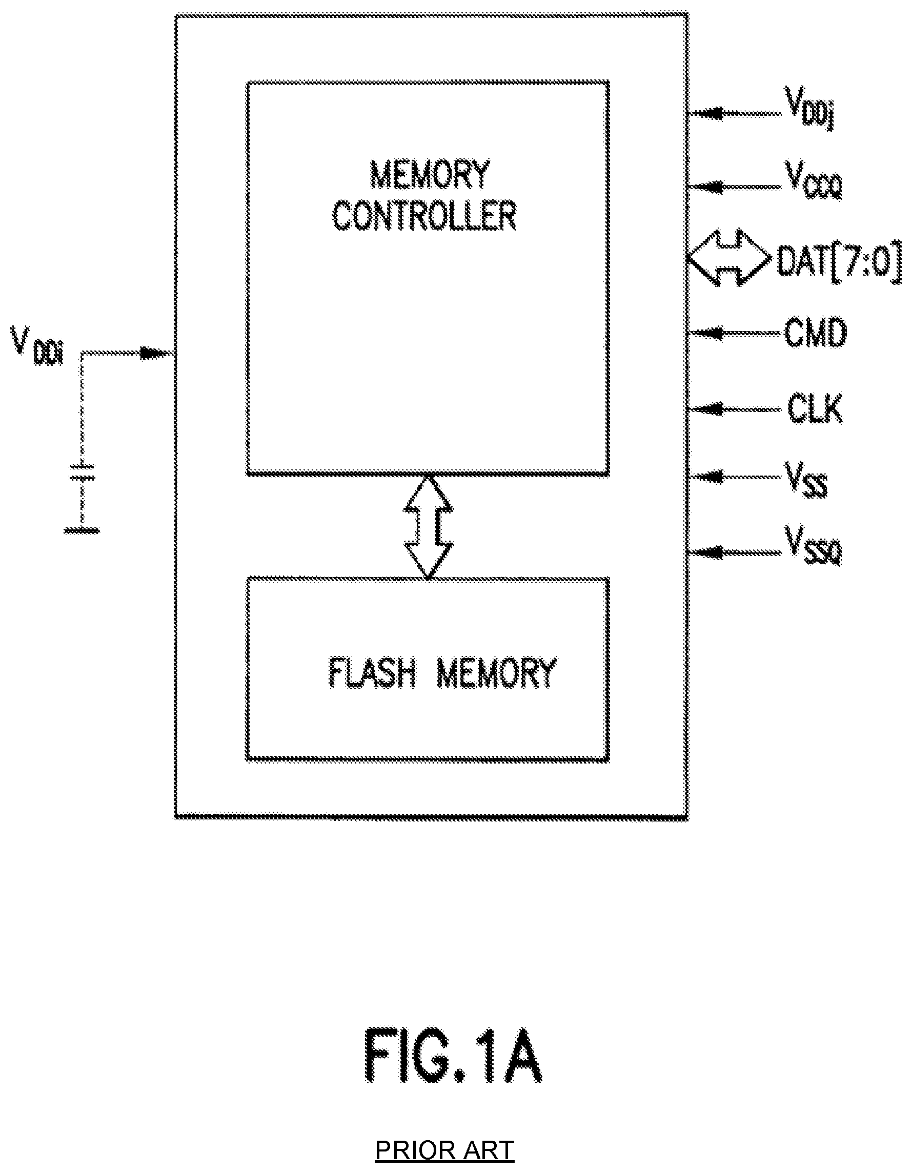
Various types of flash-based mass storage memories currently exist. A basic premise of mass storage memory is to hide the flash technology complexity from the host system. A technology such as eMMC is one example.
FIG. 1A reproduces FIG. 2 from JEDEC Standard, Embedded MultiMediaCard (eMMC) Product Standard, High Capacity, JESD84-A42, June 2007, JEDEC Solid State Technology Association, and shows a functional block diagram of an eMMC. The JEDEC eMMC includes, in addition to the flash memory itself, an intelligent on-board controller that manages the MMC communication protocol. The controller also handles block-management functions such as logical block allocation and wear leveling. The interface includes a clock (CLK) input. Also included is a command (CMD), which is a bidirectional command channel used for device initialization and command transfers. Commands are sent from a bus master to the device, and responses are sent from the device to the host. Also included is a bidirectional data bus (DAT[7:0]). The DAT signals operate in push-pull mode. By default, after power-up or RESET, only DATO is used for data transfer. The memory controller can configure a wider data bus for data transfer using either DAT[3:0] (4-bit mode) or DAT[7:0] (8-bit mode).
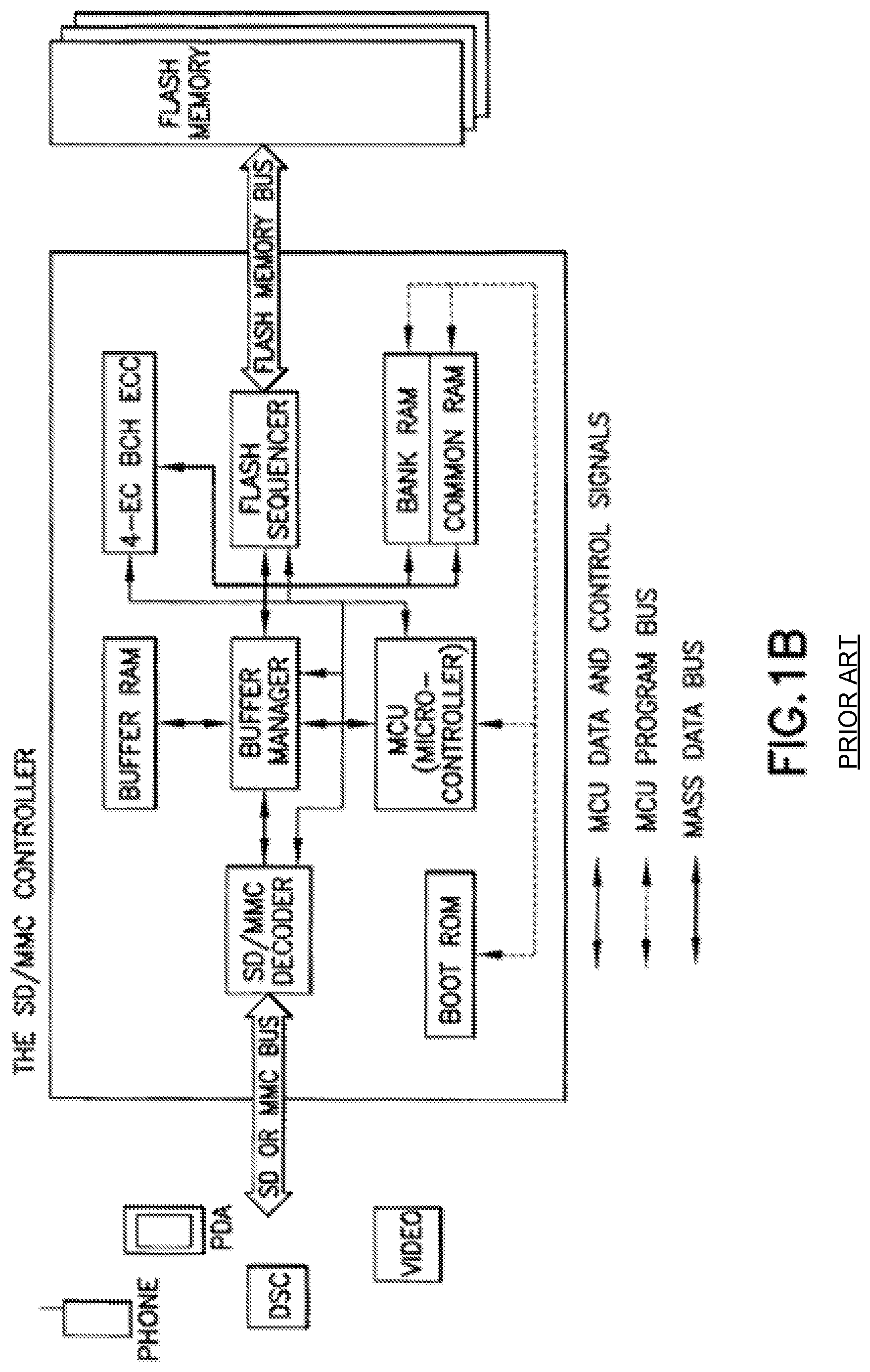
One non-limiting example of a flash memory controller construction is described in "A NAND Flash Memory Controller for SD/MMC Flash Memory Card", Chuan-Sheng Lin and Lan-Rong Dung, IEEE Transactions of Magnetics, Vol. 43, No. 2, February 2007, pp. 933-935 (hereafter referred to as Lin et al.) FIG. 1B reproduces FIG. 1 of Lin et al., and shows an overall block diagram of the NAND flash controller architecture for a SD/MMC card. The particular controller illustrated happens to use a w-bit parallel Bose-Chaudhuri-Hocquengham (BCH) error-correction code (ECC) designed to correct random bit errors of the flash memory, in conjunction with a code-banking mechanism. Of particular interest herein are the various RAM memories (e.g., buffer RAM, bank RAM, common RAM) that form part of the controller architecture.
Reference may also be made to US Patent Application Publication 2008/0228984, Sep. 18, 2008, "Single-Chip Multi-Media Card/Secure Digital (MCC/SD) Controller Reading Power-On Boot Code from Integrated Flash Memory for User Storage", I-Kang Yu et al. This publication describes another example of a flash controller where a Multi-Media Card/Secure Digital (MMC/SD) single-chip flash device contains a MMC/SD flash microcontroller and flash mass storage blocks containing flash memory arrays that are block-addressable rather than randomly-addressable. MMC/SD transactions from a host MMC/SD bus are read by a bus transceiver on the MMC/SD flash microcontroller. Various routines that execute on a CPU in the MMC/SD flash microcontroller are activated in response to commands in the MMC/SD transactions. A flash-memory controller in the MMC/SD flash microcontroller transfers data from the bus transceiver to the flash mass storage blocks for storage. Rather than booting from an internal ROM coupled to the CPU, a boot loader is transferred by direct memory access (DMA) from the first page of the flash mass storage block to an internal RAM. The flash memory is automatically read from the first page at power-on. The CPU then executes the boot loader from the internal RAM to load the control program. This approach is said to enable the microcontroller ROM to be eliminated or minimized.
Also of potential interest is an application note AN2539 "How to boot an embedded system from an eMMC.TM. equipped with a Microsoft FAT file system", Numonyx B.V., November 2008. This application note in Appendix A provides an overview of eMMC, and in Appendix B provides an overview of FAT.
SUMMARY
In a first aspect thereof the exemplary embodiments of this invention provide a method that comprises, in response to an allocation of read/write memory in a host device for use by a mass memory storage device, writing data from the mass memory storage device to the allocated read/write memory of the host device; and subsequently reading the data from the allocated memory to the mass memory storage device.
In another aspect thereof the exemplary embodiments of this invention provide an apparatus that comprises a controller; a volatile memory that is readable and writable by the controller; a non-volatile memory that is readable and writable by the controller; and an interface for connecting the apparatus to a host device. The controller is configurable to respond to an allocation of read/write memory in the host device to write data to the allocated memory of the host device, and to subsequently read the data from the allocated memory.
In another aspect thereof the exemplary embodiments of this invention provide a method that comprises allocating read/write memory in a host device for use by a mass memory storage device; receiving data from the mass memory storage device and writing the received data into the allocated read/write memory of the host device; and subsequently sending the data from the allocated memory to the mass memory storage device.
In a still further aspect thereof the exemplary embodiments of this invention provide an apparatus that comprises a controller; a memory that is readable and writable by the controller; and an interface for connecting the apparatus to a mass storage memory device. The controller is configurable to allocate a portion of the memory for use by the mass storage memory device. The controller is further configurable to receive data from the mass storage memory device and to store the received data in the allocated portion of the memory, and to subsequently send the data from the allocated portion of the memory to the mass storage memory device.
BRIEF DESCRIPTION OF THE DRAWINGS
In the attached Drawing Figures:
FIG. 1A reproduces FIG. 2 from JEDEC Standard, Embedded MultiMediaCard (eMMC) Product Standard, High Capacity, JESD84-A42, June 2007, JEDEC Solid State Technology Association, and shows a functional block diagram of an eMMC.
FIG. 1B reproduces FIG. 1 of Lin et al., and shows an example of an overall block diagram of a NAND flash controller architecture for a SD/MMC card.
FIG. 2 is a simplified block diagram of a host device connected with a mass storage memory device, and is helpful in describing the exemplary embodiments of this invention.
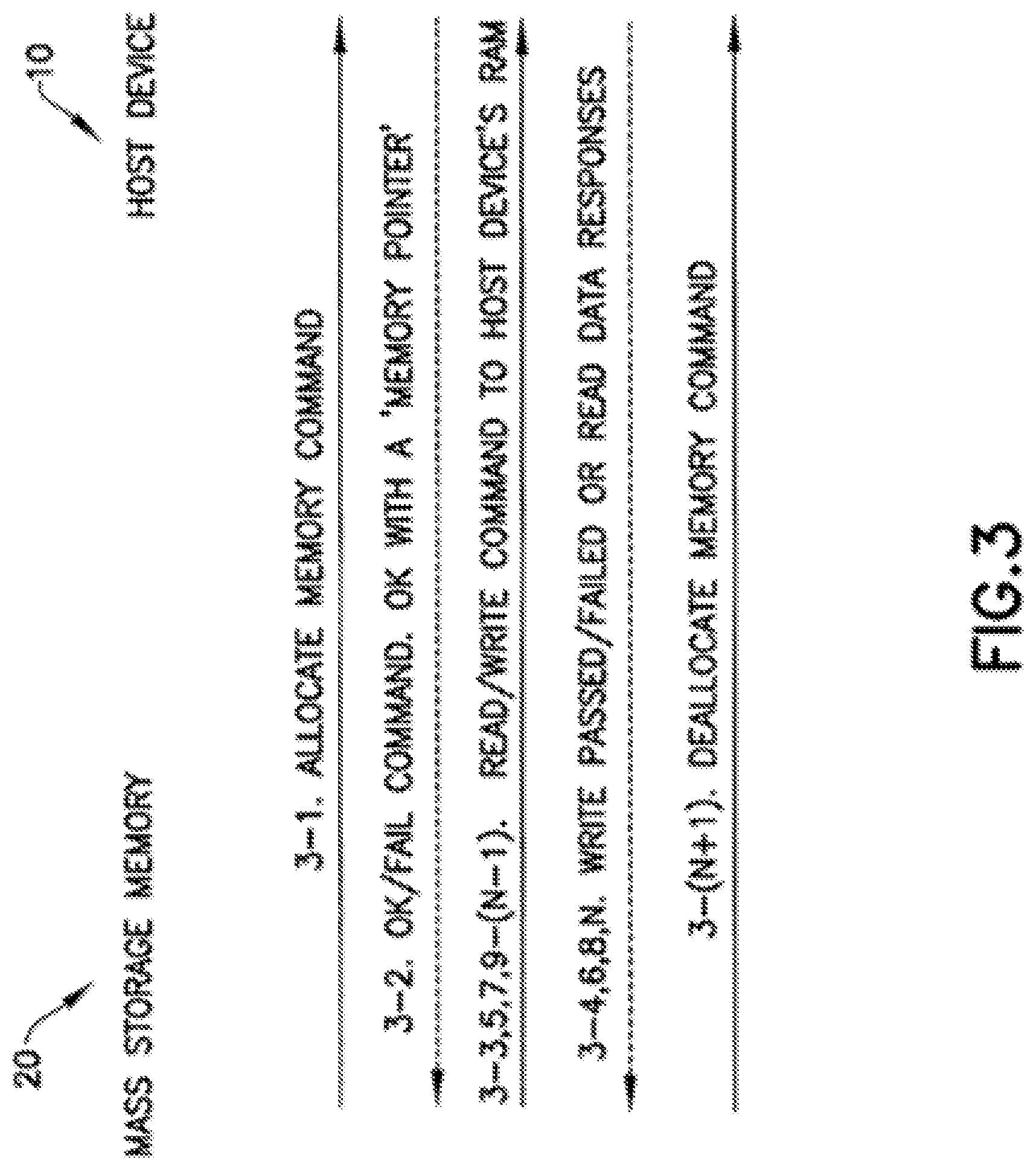
FIG. 3 is a signal/message flow diagram that describes an exemplary embodiment of this invention for the mass storage memory device of FIG. 2 to allocate, use and de-allocate RAM of the host device.
FIG. 4 is a signal/message flow diagram that describes another exemplary embodiment of this invention, where the mass storage memory device of FIG. 2 has a built-in file system.
FIG. 5 shows a block diagram of one exemplary embodiment of the host device when embodied as a wireless communication device.
FIG. 6 is a logic flow diagram that illustrates the operation of a method, and a result of execution of computer program instructions embodied on a computer readable memory, in accordance with the exemplary embodiments of this invention.
FIG. 7 is a logic flow diagram that illustrates the operation of a method, and a result of execution of computer program instructions embodied on a computer readable memory, further in accordance with the exemplary embodiments of this invention.
DETAILED DESCRIPTION
At present, most mass storage memories provide LBA-based access, e.g., eMMC and different types of external memory cards such as SD. However, it may also be the case that the entire file system (FS) SW is embedded in the mass storage memory device.
When a mass storage memory is used in a high volume consumer device, such as a mobile wireless communication device, one important consideration is cost, and one factor affecting the cost is the amount of RAM in the mass storage memory device itself.
Another important consideration is performance. The overall performance depends on many factors. For example, for lengthy (time consuming) operations (in particular if the mass storage memory device contains an entire file system SW) there would be an advantage to include a substantial amount of RAM in the mass storage memory device. However, this can have a negative impact on the cost.
It may be the case that system context (metadata) would be stored in the flash memory of the mass storage memory device. However, this approach has several associated disadvantages. For example, repeatedly writing the system context (metadata) to the mass storage memory device raises wearing issues that can impact the usable life of the mass storage memory device. Also, writing data to the flash memory can be a relatively slow process.
Another important consideration is the power efficiency. To provide good power efficiency the mass storage memories are preferably shutdown (powered-off) when not needed (meaning also that the internal RAM of the device is preferably shutdown as well). However, and assuming that the RAM is volatile in nature, then whatever data is stored in the RAM is lost when the power is removed from the RAM. To then perform re-initialization after power-up all needed information (e.g., logical-to-physical mapping information and/or file system structures) need to be restored. A full re-initialization of a LBA mass storage memory may require a substantial (and user-noticeable) amount of time (e.g., up to one second with an SD card), and entire file system initialization (if the file system is resident in the mass storage memory) may take even longer. Therefore, it is desirable to retain internal device context over the power-off/power-on cycle.
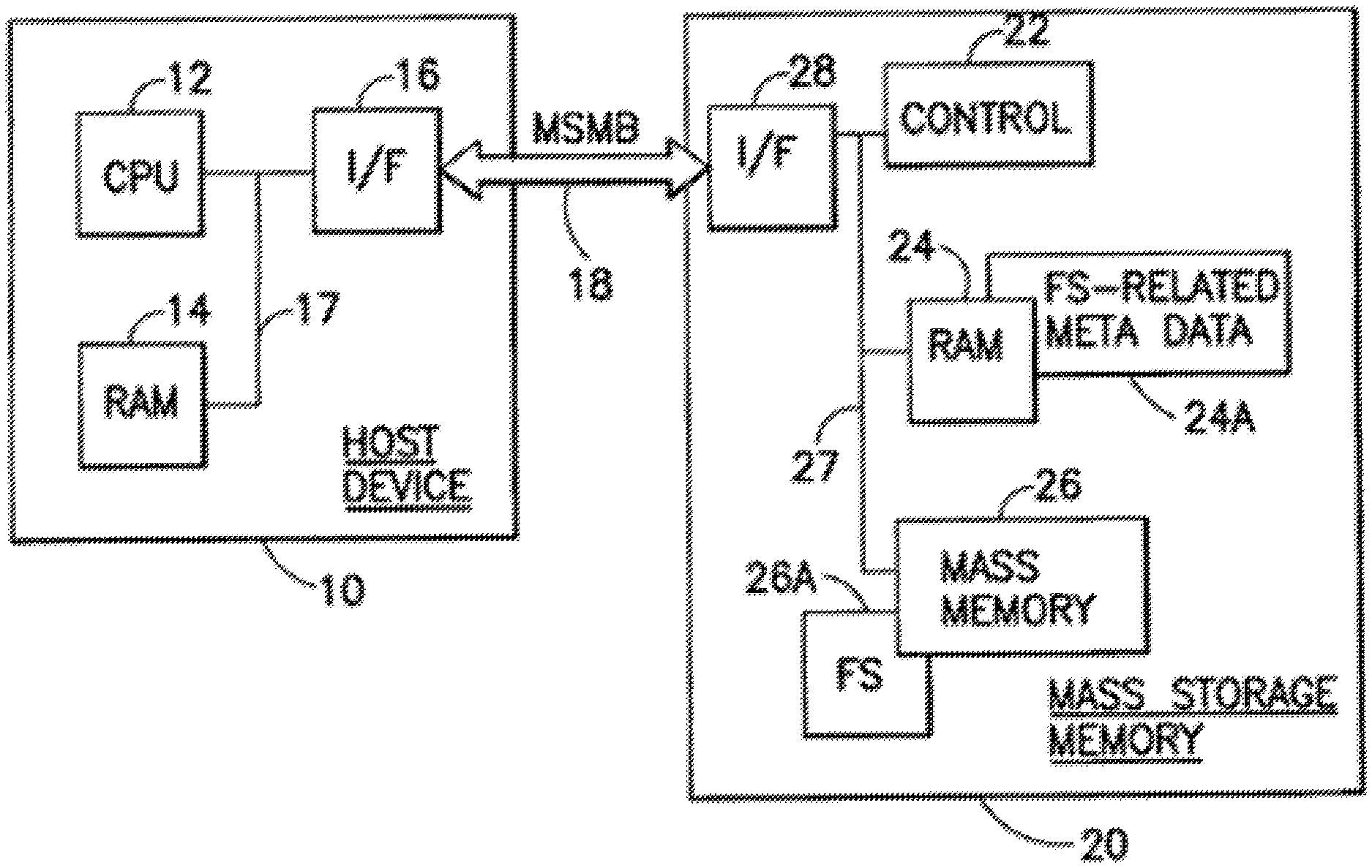
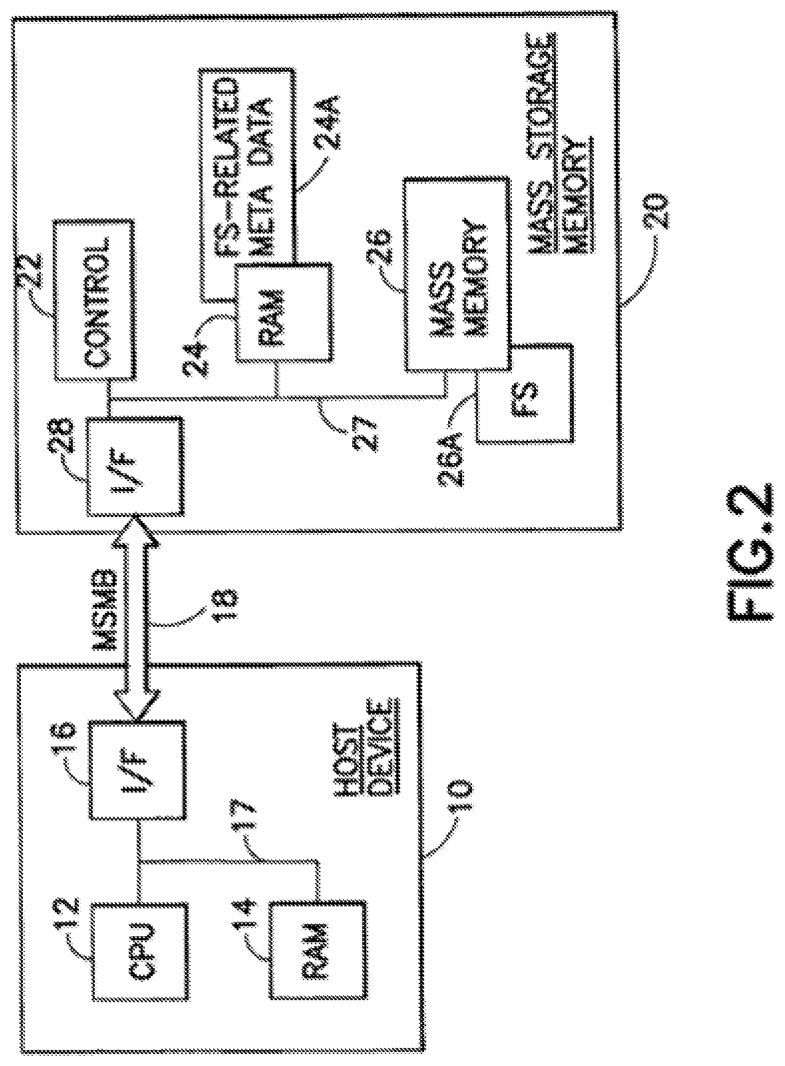
Before further describing the exemplary embodiments of this invention, reference is made to FIG. 2 which shows is a simplified block diagram of a host system or device 10 connected with a mass storage memory 20 via a mass storage memory bus (MSMB) 18. The MSMB 18 may be compatible with any suitable mass memory interface standard such as MMC or UFS, as two non-limiting examples. The MSMB 18 may include signal lines such as those shown in FIG. 1A for an eMMC embodiment. The host device 10 includes at least one controller, such as a CPU 12 that operates in accordance with stored program instructions. The program instructions may be stored in a RAM 14 or in another memory or memories. The CPU 12 is connected with the RAM 14 and a MSMB interface (I/F) 16 via at least one internal bus 17. The MSMB interface 16 may include a memory controller (MC), or may be coupled with a MC unit associated with the CPU 12. The host device 10 may be a computer, a cellular phone, a digital camera, a gaming device or a PDA, as several non-limiting examples. Note that the RAM 14 may be any read/write memory or memory device, such as semiconductor memory or a disk-based memory.
The mass storage memory 20 includes a microcontroller or, more simply, a controller 22 that is connected via at least one internal bus 27 with a volatile RAM 24, a non-volatile mass memory 26 (e.g., a multi-gigabyte flash memory mass storage) and a MSMB interface (I/F) 28. The controller 22 operates in accordance with stored program instructions. The program instructions may be stored in the RAM 24 or in a ROM or in the mass memory 26. The mass storage memory 20 may be embodied as an MMC, eMMC or a SD device, as non-limiting examples, and may be external to (plugged into) the host device 10 or installed within the host device 10. Note that the mass memory 26 may, in some embodiments, store a file system (FS) 26A. In this case then the RAM 24 may store FS-related metadata 24A, such as one or more data structures comprised of bit maps, file allocation table data and/or other FS-associated information.
The exemplary embodiments of this invention provide a technique to share the RAM 14 of the host device 10 with the mass storage memory device 20. It may be assumed that the host device 10 (e.g., a mobile computer, a cellular phone, a digital camera, a gaming device, a PDA, etc.) has the capability to allocate and de-allocate the RAM 14. As will be discussed in further detail below, the allocation of the RAM 14 may be performed dynamically or it may be performed statically. The allocation of a portion of the RAM may be performed in response to a request received at the host device 10, or at the initiative of the host device 10.
In the exemplary embodiments of this invention the RAM 14 allocation is provided for the mass storage memory 20 (connected via the MSMB 18 to the host CPU 12), if the mass storage memory 20 has a need to extend its own RAM 24 space and/or if the mass storage memory 20 has a need for non-volatile RAM (the contents of which are not lost when the mass storage memory 20 is powered-off). It is also within the scope of the exemplary embodiments of this invention for the mass storage memory 20 to read and/or write (R/W) allocated RAM 14 in the host device 10. The allocation/de-allocation and R/W access methods may be implemented by extensions to a command set used to communicate with the mass storage memory 20 via an applicable mass storage memory protocol.
In accordance with certain exemplary embodiments of this invention the mass storage memory device 20 is provided with a mechanism to interrupt/send a message to host device 10 to initiate an allocation of space in the RAM 14. The interrupt/message is sent over the MSMB 18, and may be considered as an extension to current command sets. Referring to FIG. 3, an allocate memory command is sent during operation 3-1. If the allocation request succeeds (indicated during operation 3-2) the controller 22 is enabled to extend its own RAM 24 with the RAM 14 of the host device 10. The mass storage memory device 20 may store, for example, large tables into the RAM 14 using a RAM WRITE command (a newly specified command), or it may fetch data from the host device RAM 14 using a RAM READ command (another newly specified command). The read or write operation is shown as interleaved operations 3-3, 3-4, 3-5, 3-6, . . . , 3-(N-1), 3-N. When the mass storage memory device 20 completes the operation with the RAM 14 it may free the host device RAM 14 using another newly specified command that requests that the host 10 RAM memory be de-allocated (operation 3-(N+1)).
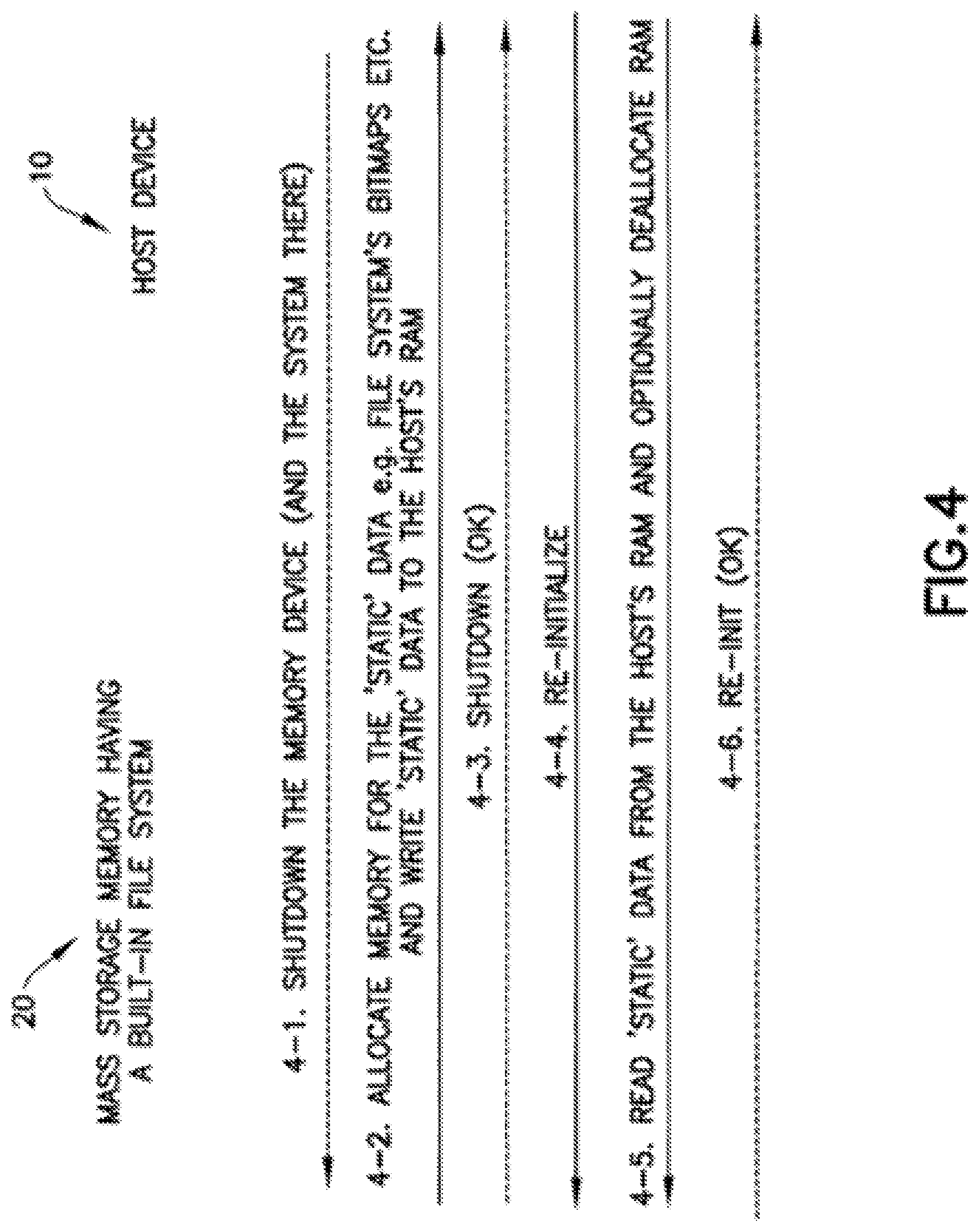
FIG. 4 illustrates a further exemplary embodiment that utilizes the host system RAM 14 for the mass storage memory 26 having a built-in file system, such as the FS 26A shown in FIG. 2. First the host system 10 sends a SHUTDOWN command to the mass storage memory device 20 (operation 4-1). Next the mass storage memory device 20 allocates RAM 14 from the host 10 and then loads (stores using a RAM WRITE command) all vital `static` file system-related data (meta-data 24A) into host RAM 14 (operation 4-2). `Static` data in this context may be, for example, various bitmaps, such as an allocation bitmap in the exFAT or ext3 file systems. This data may be processed (e.g., at least one of sorted, arranged and filtered) by the CPU 12 (controller) of the host device, and may include data from a large number of sectors in the mass storage memory 26. Mass memory storage device 20 may then send a shutdown OK indication (operation 4-3). The host 10 can remove power from the mass memory storage device 20, and the device 20 may be physically removed from the MSMB 18. Re-initialization (operations 4-4, 4-5, 4-6) of the mass storage memory device 20 is performed when host device 10 needs to get/put certain data from or into the mass storage memory device 20. Re-initialization of the mass storage memory 26 (and the file system 26A) may be sped up by using the sorted/arranged/filtered read data from the RAM 14. When the re-initialization operation is completed the mass storage memory device 20 may de-allocate the used RAM 14 in the host device 10, or the RAM 14 may not be de-allocated thereby reserving the RAM space for future use by the mass storage memory device 20.
It should be noted that in other exemplary embodiments of this invention the allocation of host RAM 14 may occur differently. For example, the host device 10 may allocate RAM 14 dynamically and pass a `pointer` to the allocated RAM to the mass storage memory device 20. It is then up to the controller 22 of the mass storage memory device 20 how to utilize the allocated host RAM 14. Note that in this embodiment an explicit allocation request from the mass storage memory device 20 may not be sent to the host device 10. Instead, the host device 10 may on its own initiative allocate a portion of the RAM 14, such as when it first detects the presence of the mass memory storage device 20. Of course, subsequent signaling between the mass storage memory device 20 and the host device 10 may be used to change the size of the allocated RAM 14 if the initial allocation is not sufficient for the needs of the controller 22. As another example of RAM 14 allocation, a portion of the RAM 14 may be allocated by the host 10 in a static manner, and the mass storage memory device 20 then simply uses the same portion of the RAM 14 each time it needs to extend the RAM 24. In this case the mass storage memory device 20 may already have knowledge of the location/size of the allocated RAM 14, and a pointer is not needed to be sent from the host device 10.
Note that while it may typically be the case that the mass storage memory device 20 will receive an allocation of host memory to store contents of the volatile RAM 24, in general the allocation may be for storing data for any read/write memory contained within the mass storage memory device 20.
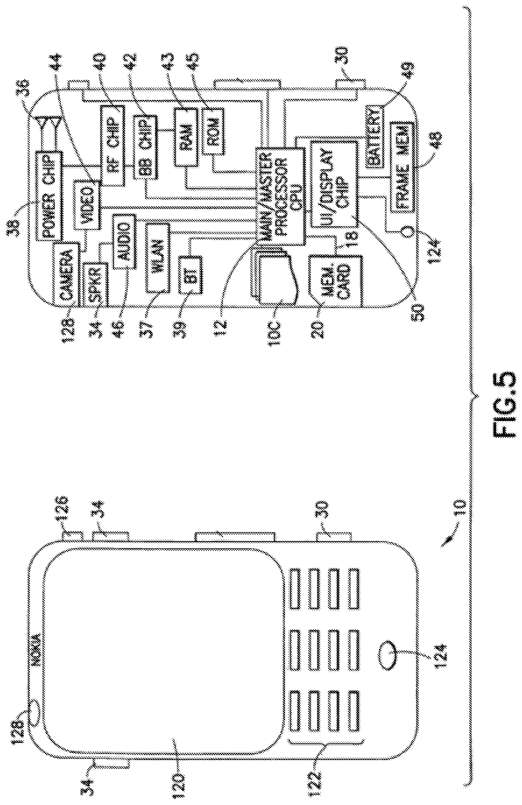
FIG. 5 illustrates one non-limiting embodiment of the host device 10 used with the mass storage memory device 20, referred to in FIG. 5 simply as a memory card. In this exemplary embodiment the host device is embodied as a user equipment (UE), shown in both plan view (left) and sectional view (right). In FIG. 5 the UE 10 has a graphical display interface 120 and a user interface 122 illustrated as a keypad but understood as also encompassing touch screen technology at the graphical display interface 120 and voice recognition technology received at the microphone 124. A power actuator 126 controls the device being turned on and off by the user. The exemplary UE 10 may have a camera 128 which is shown as being forward facing (e.g., for video calls) but may alternatively or additionally be rearward facing (e.g., for capturing images and video for local storage). The camera 128 is controlled by a shutter actuator 30 and optionally by a zoom actuator which may alternatively function as a volume adjustment for the speaker(s) 34 when the camera 128 is not in an active mode.
Within the sectional view of FIG. 5 are seen multiple transmit/receive antennas 36 that are typically used for cellular communication. The antennas 36 may be multi-band for use with other radios in the UE. The operable ground plane for the antennas 36 is shown by shading as spanning the entire space enclosed by the UE housing though in some embodiments the ground plane may be limited to a smaller area, such as disposed on a printed wiring board on which the power chip 38 is formed. The power chip 38 controls power amplification on the channels being transmitted and/or across the antennas that transmit simultaneously where spatial diversity is used, and amplifies the received signals. The power chip 38 outputs the amplified received signal to a radio frequency (RF) chip 40 which demodulates and downconverts the signal for baseband processing. A baseband (BB) chip 42 detects the signal which is then converted to a bit stream and finally decoded. Similar processing occurs in reverse for signals generated in the host device 10 and transmitted from it.
Signals going to and from the camera 128 may pass through an image/video processor 44 that encodes and decodes the various image frames. A separate audio processor 46 may also be present controlling signals to and from the speakers 34 and the microphone 124. The graphical display interface 120 is refreshed from a frame memory 48 as controlled by a user interface chip 50 which may process signals to and from the display interface 20 and/or additionally process user inputs from the keypad 22 and elsewhere.
Certain embodiments of the UE 10 may also include one or more secondary radios such as a wireless local area network radio WLAN 37 and a Bluetooth? radio 39, which may incorporate an antenna on the chip or be coupled to an antenna off the chip. Throughout the apparatus are various memories such as random access memory RAM 43, read only memory ROM 45, and in some embodiments removable memory such as the illustrated memory card 20 on which various programs 10C may be stored. All of these components within the UE 10 are normally powered by a portable power supply such as a battery 49.
The processors 38, 40, 42, 44, 46, 50, if embodied as separate entities in a UE 10, may operate in a slave relationship to the main processor (CPU) 12, which may then be in a master relationship to them. Certain embodiments may be disposed across various chips and memories as shown, or disposed within another processor that combines some of the functions described above for FIG. 5. Any or all of these various processors of FIG. 5 access one or more of the various memories, which may be on chip with the processor or separate from the chip with the processor. Note that the various integrated circuits (e.g., chips 38, 40, 42, etc.) that were described above may be combined into a fewer number than described and, in a most compact case, may all be embodied physically within a single chip.
In this exemplary embodiment the CPU 12 of the UE 10 (the host device) operates with the memory card 20 (the mass storage memory device) as described above with respect to FIGS. 3 and 4 so that the RAM 24 of the memory card 20 may be extended to use the RAM 14 of the UE 10.
There are a number of technical effects that may be realized by the use of the exemplary embodiments of the invention. For example, there is provided a cost efficient way to extend RAM in the mass storage memory device 20. Further by example, the mass storage memory device 20 may be powered off, while retaining mass storage memory device information on the RAM 14 of the host system.
Based on the foregoing it should be apparent that the exemplary embodiments of this invention provide a method, apparatus and computer program(s) to extend the RAM of a mass storage memory device to include the RAM of an attached host device.
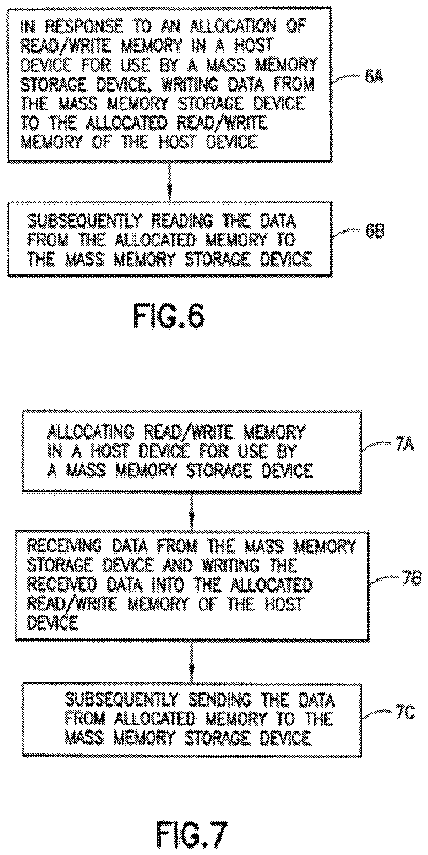
FIG. 6 is a logic flow diagram that illustrates the operation of a method, and a result of execution of computer program instructions, in accordance with the exemplary embodiments of this invention. In accordance with these exemplary embodiments a method performs, at Block 6A, in response to an allocation of read/write memory in a host device for use by a mass memory storage device, writing data from the mass memory storage device to the allocated read/write memory of the host device. At Block 6B there is an operation of subsequently reading the data from the allocated memory to the mass memory storage device.
FIG. 7 is a logic flow diagram that illustrates the operation of a method, and a result of execution of computer program instructions, in accordance with the exemplary embodiments of this invention. In accordance with these exemplary embodiments a method performs, at Block 7A, an operation of allocating read/write memory in a host device for use by a mass memory storage device. At Block 7B there is an operation of receiving data from the mass memory storage device and writing the received data into the allocated read/write memory of the host device. At Block 7C there is an operation of subsequently sending the data from the allocated memory to the mass memory storage device.
The various blocks shown in FIGS. 6 and 7 may be viewed as method steps, and/or as operations that result from operation of computer program code, and/or as a plurality of coupled logic circuit elements constructed to carry out the associated function(s).
In general, the various exemplary embodiments may be implemented in hardware or special purpose circuits, software, logic or any combination thereof. For example, some aspects may be implemented in hardware, while other aspects may be implemented in firmware or software which may be executed by a controller, microprocessor or other computing device, although the invention is not limited thereto. While various aspects of the exemplary embodiments of this invention may be illustrated and described as block diagrams, flow charts, or using some other pictorial representation, it is well understood that these blocks, apparatus, systems, techniques or methods described herein may be implemented in, as non-limiting examples, hardware, software, firmware, special purpose circuits or logic, general purpose hardware or controller or other computing devices, or some combination thereof.
It should thus be appreciated that at least some aspects of the exemplary embodiments of the inventions may be practiced in various components such as integrated circuit chips and modules, and that the exemplary embodiments of this invention may be realized in an apparatus that is embodied as an integrated circuit. The integrated circuit, or circuits, may comprise circuitry (as well as possibly firmware) for embodying at least one or more of a data processor or data processors, a digital signal processor or processors, baseband circuitry and radio frequency circuitry that are configurable so as to operate in accordance with the exemplary embodiments of this invention.
Various modifications and adaptations to the foregoing exemplary embodiments of this invention may become apparent to those skilled in the relevant arts in view of the foregoing description, when read in conjunction with the accompanying drawings. However, any and all modifications will still fall within the scope of the non-limiting and exemplary embodiments of this invention.
It should be noted that the terms "connected," "coupled," or any variant thereof, mean any connection or coupling, either direct or indirect, between two or more elements, and may encompass the presence of one or more intermediate elements between two elements that are "connected" or "coupled" together. The coupling or connection between the elements can be physical, logical, or a combination thereof. As employed herein two elements may be considered to be "connected" or "coupled" together by the use of one or more wires, cables and/or printed electrical connections, as well as by the use of electromagnetic energy, such as electromagnetic energy having wavelengths in the radio frequency region, the microwave region and the optical (both visible and invisible) region, as several non-limiting and non-exhaustive examples.
Furthermore, some of the features of the various non-limiting and exemplary embodiments of this invention may be used to advantage without the corresponding use of other features. As such, the foregoing description should be considered as merely illustrative of the principles, teachings and exemplary embodiments of this invention, and not in limitation thereof
* * * * *
D00000
D00001
D00002
D00003
D00004
D00005
D00006
D00007
XML
uspto.report is an independent third-party trademark research tool that is not affiliated, endorsed, or sponsored by the United States Patent and Trademark Office (USPTO) or any other governmental organization. The information provided by uspto.report is based on publicly available data at the time of writing and is intended for informational purposes only.
While we strive to provide accurate and up-to-date information, we do not guarantee the accuracy, completeness, reliability, or suitability of the information displayed on this site. The use of this site is at your own risk. Any reliance you place on such information is therefore strictly at your own risk.
All official trademark data, including owner information, should be verified by visiting the official USPTO website at www.uspto.gov. This site is not intended to replace professional legal advice and should not be used as a substitute for consulting with a legal professional who is knowledgeable about trademark law.