Vacuum suction apparatus
Wu , et al. April 13, 2
U.S. patent number 10,978,332 [Application Number 15/716,366] was granted by the patent office on 2021-04-13 for vacuum suction apparatus. This patent grant is currently assigned to Prilit Optronics, Inc.. The grantee listed for this patent is Himax Technologies Limited, Prilit Optronics, Inc.. Invention is credited to Tzung-Ren Wang, Biing-Seng Wu, Chao-Wen Wu.


View All Diagrams
| United States Patent | 10,978,332 |
| Wu , et al. | April 13, 2021 |
Vacuum suction apparatus
Abstract
A vacuum suction apparatus includes a semiconductor substrate with a top portion having grooves and a bottom portion having through holes, wherein each said groove correspondingly connects with at least one said through hole, and the groove has a width greater than a width of the through hole; and a cover plate disposed on a top surface of the semiconductor substrate. At least one edge of the vacuum suction apparatus has a vacuum chamber, which connects with the grooves. In another embodiment, the cover plate is replaced with a vacuum cover disposed above the semiconductor substrate, wherein the vacuum cover and the semiconductor substrate construct a vacuum chamber.
| Inventors: | Wu; Biing-Seng (Tainan, TW), Wu; Chao-Wen (Tainan, TW), Wang; Tzung-Ren (Tainan, TW) | ||||||||||
|---|---|---|---|---|---|---|---|---|---|---|---|
| Applicant: |
|
||||||||||
| Assignee: | Prilit Optronics, Inc. (Tainan,
TW) |
||||||||||
| Family ID: | 1000005486859 | ||||||||||
| Appl. No.: | 15/716,366 | ||||||||||
| Filed: | September 26, 2017 |
Prior Publication Data
| Document Identifier | Publication Date | |
|---|---|---|
| US 20180096878 A1 | Apr 5, 2018 | |
Foreign Application Priority Data
| Oct 5, 2016 [TW] | 105132128 | |||
| Mar 15, 2017 [TW] | 106108614 | |||
| Current U.S. Class: | 1/1 |
| Current CPC Class: | H01L 21/6838 (20130101); H01L 33/0095 (20130101); H01L 21/67144 (20130101); H01L 25/0753 (20130101); H01L 21/6875 (20130101) |
| Current International Class: | H01L 21/683 (20060101); H01L 21/67 (20060101); H01L 33/00 (20100101); H01L 25/075 (20060101); H01L 21/687 (20060101) |
| Field of Search: | ;269/20,21 |
References Cited [Referenced By]
U.S. Patent Documents
| 5443012 | August 1995 | Underbrink |
| 5803797 | September 1998 | Piper |
| 5857667 | January 1999 | Lee |
| 6586886 | July 2003 | Katz |
| 8070199 | December 2011 | Na |
| 2003/0047289 | March 2003 | Jaussaud |
| 2005/0014390 | January 2005 | Li |
| 2007/0158031 | July 2007 | Miyake |
| 2007/0252970 | November 2007 | Shibazaki |
| 2008/0276864 | November 2008 | Koelmel |
| 2011/0183108 | July 2011 | Tachibana |
| 2012/0009660 | January 2012 | Pottathil |
| 2012/0171815 | July 2012 | Maeng |
| 2013/0075982 | March 2013 | Simmons et al. |
| 2013/0095613 | April 2013 | Tanaka |
| 2013/0168910 | July 2013 | Sun |
| 2015/0151411 | June 2015 | Veis |
| 2015/0261102 | September 2015 | Lof |
| 2016/0020132 | January 2016 | Yudovsky |
| 2016/0195579 | July 2016 | Simmons |
| 2017/0080548 | March 2017 | Xu |
| 2017/0084477 | March 2017 | Kang |
| 2017/0266943 | September 2017 | Utsugi |
| 2017/0297920 | October 2017 | Richardson |
| 2017/0345702 | November 2017 | Iwabuchi |
| 2019/0019718 | January 2019 | Wu |
| 2019/0221467 | July 2019 | Scholz-Goerlach |
| 2017022269 | Jul 2015 | JP | |||
Other References
|
Office Action dated Aug. 26, 2020 in corresponding Indian Patent Application No. 201714034565. cited by applicant. |
Primary Examiner: Hall, Jr.; Tyrone V
Assistant Examiner: Nejad; Mahdi H
Attorney, Agent or Firm: Stout; Donald E. Stout, Uxa & Buyan, LLP
Claims
What is claimed is:
1. A vacuum suction apparatus, comprising: a semiconductor substrate with a top portion having a plurality of first grooves and a bottom portion having a plurality of through holes, each first groove of said plurality of first grooves correspondingly connecting with at least one through hole of said plurality of through holes, and each first groove of the plurality of first grooves having a width greater than a width of each through hole of the plurality of through holes; and a cover plate disposed on a top surface of the semiconductor substrate; wherein a vacuum chamber, connecting with the plurality of first grooves, is disposed on at least one edge of the vacuum suction apparatus; wherein each first groove of the plurality of first grooves is a continuous groove disposed longitudinally, each continuous groove of said plurality of first continuous grooves correspondingly connecting with the at least one through hole of the plurality of through holes, and the first grooves of a same longitudinal line being connected directly but the first grooves belonging to different longitudinal lines being not connected directly; wherein the bottom portion of the semiconductor substrate includes a replaceable buffer layer, from which the plurality of through holes pass; wherein the bottom portion of the semiconductor substrate has a plurality of second grooves disposed between adjacent through holes of the plurality of through holes, each second groove of the plurality of second grooves having a width greater than a width of a miniature device.
2. The apparatus of claim 1, wherein the semiconductor substrate comprises a silicon wafer.
3. The apparatus of claim 1, wherein each continuous first groove of the plurality of grooves has a side being sloped and narrowed towards the corresponding at least one through hole of the plurality of through holes.
4. The apparatus of claim 1, wherein the vacuum chamber is perpendicular to the plurality of continuous grooves and directly connects with the plurality of continuous grooves.
5. The apparatus of claim 1, wherein a diameter size of each of the plurality of through holes is smaller than 10 micrometers, and a lateral width of each continuous groove of the plurality of continuous grooves is smaller than 100 micrometers.
6. The apparatus of claim 1, wherein each second groove of the plurality of the second grooves is a continuous groove disposed longitudinally and/or laterally at the bottom portion of the semiconductor substrate.
7. The apparatus of claim 1, wherein each second groove of the plurality of the second grooves is a discontinuous groove, arranged in matrix form, disposed at the bottom portion of the semiconductor substrate.
8. The apparatus of claim 1, wherein the cover plate comprises a silicon wafer.
9. The apparatus of claim 1, wherein the cover plate comprises glass.
10. The apparatus of claim 1, wherein the cover plate comprises sapphire.
11. A vacuum suction apparatus, comprising: a semiconductor substrate with a top portion having a plurality of first grooves and a bottom portion having a plurality of through holes, each first groove of said plurality of first grooves correspondingly connecting with at least one through hole of said plurality of through holes, and each first groove of the plurality of first grooves having a width greater than a width of each through hole of the plurality of through holes; and a vacuum cover disposed above the semiconductor substrate the vacuum cover and the semiconductor substrate defining a vacuum chamber; wherein each first groove of the plurality of first grooves is a continuous groove disposed longitudinally, each continuous groove of said plurality of first continuous grooves correspondingly connecting with the at least one through hole of the plurality of through holes, and the first grooves of a same longitudinal line being connected directly but the first grooves belonging to different longitudinal lines being not connected directly; wherein the bottom portion of the semiconductor substrate includes a replaceable buffer layer, from which the plurality of through holes pass; at least one post, disposed between a bottom surface of the vacuum cover and a top surface of the semiconductor substrate, for supporting the vacuum cover.
12. The apparatus of claim 11, wherein the vacuum cover comprises a silicon wafer.
13. The apparatus of claim 11, wherein the vacuum cover comprises glass.
14. The apparatus of claim 11, wherein the vacuum cover comprises sapphire.
15. The apparatus of claim 11, wherein the bottom portion of the semiconductor substrate has a plurality of second grooves disposed between adjacent through holes of the plurality of through holes, each second groove of the plurality of second grooves having a width greater than a width of a miniature device.
16. The apparatus of claim 15, wherein each second groove of the plurality of the second grooves is a continuous groove disposed longitudinally and/or laterally at the bottom portion of the semiconductor substrate.
17. The apparatus of claim 15, wherein each second groove of the plurality of the second grooves is a discontinuous groove, arranged in matrix form, disposed at the bottom portion of the semiconductor substrate.
18. The apparatus of claim 11, wherein the semiconductor substrate comprises a silicon wafer.
Description
CROSS-REFERENCE TO RELATED APPLICATIONS
This application claims priority of Taiwan Application No. 105132128, filed on Oct. 5, 2016, and Taiwan Application No. 106108614, filed on Mar. 15, 2017, the entire contents of which are hereby incorporated by reference.
BACKGROUND OF THE INVENTION
1. Field of the Invention
The present invention generally relates to vacuum suction apparatus, and more particularly to vacuum suction apparatus adaptable to transferring micro light-emitting diodes (microLEDs).
2. Description of Related Art
A micro light-emitting diode (microLED, mLED or .mu.LED) display panel is one of flat display panels, and is composed of microscopic microLEDs each having a size of 1-10 micrometers. Compared to conventional liquid crystal display panels, the microLED display panels offer better contrast, response times and energy efficiency. Although both organic light-emitting diodes (OLEDs) and microLEDs possess good energy efficiency, the microLEDs, based on group III/V (e.g., GaN) LED technology, offer higher brightness, higher luminous efficacy and longer lifespan than the OLEDs.
During manufacturing a microLED display panel, individual microLEDs should be picked up and transferred to a display panel by magnetic force or vacuum suction force. Take vacuum suction apparatus as an example, the ratio of height to inner diameter of a suction nozzle should be less than a threshold value in order to ensure suction capability. As the size of the microLED is small, the inner diameter and the associated height of the suction nozzle should be small enough. As a result, the vacuum suction apparatus in operation is apt to deformation or even fracture, thereby reducing suction efficiency.
A need has thus arisen to propose novel vacuum apparatus in order to increase suction efficiency and enhance robustness and reliability.
SUMMARY OF THE INVENTION
In view of the foregoing, it is an object of the embodiment of the present invention to provide vacuum suction apparatus with scalability in operation, increased suction capability and efficiency, and enhanced robustness and reliability.
According to one embodiment, a vacuum suction apparatus includes a semiconductor substrate and a cover plate. The semiconductor substrate includes a top portion having a plurality of first grooves and a bottom portion having a plurality of through holes, each first groove correspondingly connecting with at least one through hole, and the first groove having a width greater than a width of the through hole. The cover plate is disposed on a top surface of the semiconductor substrate. A vacuum chamber, connecting with the first grooves, is disposed on at least one edge of the vacuum suction apparatus. In one embodiment, the first grooves are continuous grooves disposed longitudinally, each continuous groove correspondingly connecting with the through holes. The vacuum chamber is perpendicular to the continuous grooves and directly connects with the continuous grooves. In another embodiment, the first grooves are discontinuous grooves arranged in matrix form, each discontinuous groove correspondingly connecting with one through hole. Channels are connected between adjacent discontinuous grooves, and the vacuum chamber is connected with the discontinuous grooves via the channels.
According to another embodiment, a vacuum suction apparatus includes a semiconductor substrate and a vacuum cover. The semiconductor substrate includes a top portion having a plurality of first grooves and a bottom portion having a plurality of through holes, each first groove correspondingly connecting with at least one through hole, and the first groove having a width greater than a width of the through hole. The vacuum cover is disposed above the semiconductor substrate, the vacuum cover and the semiconductor substrate defining a vacuum chamber.
BRIEF DESCRIPTION OF THE DRAWINGS
FIG. 1A shows a top view illustrated of vacuum suction apparatus according to a first embodiment of the present invention;
FIG. 1B shows a bottom view of the vacuum suction apparatus of FIG. 1A;
FIG. 1C shows a side view of the vacuum suction apparatus of FIG. 1A;
FIG. 2A to FIG. 2D show cross-sectional views along section lines of FIG. 1B, respectively;
FIG. 3A schematically exemplifies microLEDs before transfer;
FIG. 3B exemplifies the through holes of the vacuum suction apparatus;
FIG. 3C and FIG. 3D show some microLEDs are picked up by the vacuum suction apparatus;
FIG. 4A shows a top view illustrated of vacuum suction apparatus according to a second embodiment of the present invention;
FIG. 4B shows a bottom view of the vacuum suction apparatus of FIG. 4A;
FIG. 4C shows a side view of the vacuum suction apparatus of FIG. 4A;
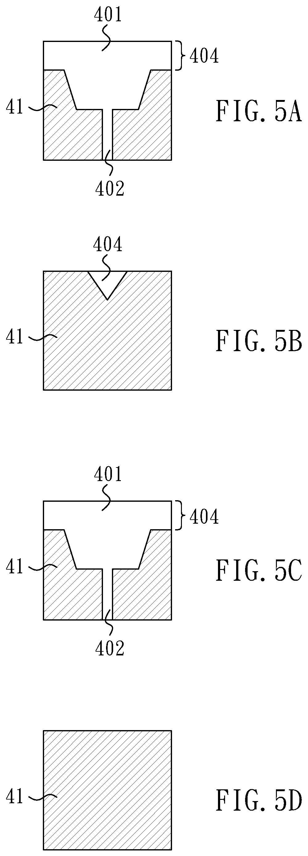
FIG. 5A to FIG. 5D show cross-sectional views along section lines of FIG. 4A, respectively;
FIG. 6A shows a cross-sectional view of vacuum suction apparatus according to a third embodiment of the present invention;
FIG. 6B shows a bottom view of the vacuum suction apparatus of FIG. 6A;
FIG. 6C shows another bottom view of the vacuum suction apparatus of FIG. 6A;
FIG. 6D shows a cross-sectional view of vacuum suction apparatus according to a modified third embodiment of the present invention;
FIG. 7A shows a cross-sectional lateral view of the first embodiment of the present invention;
FIG. 7B shows a cross-sectional lateral view of a modified first embodiment of the present invention;
FIG. 8A shows a cross-sectional lateral view of the second embodiment of the present invention; and
FIG. 8B shows a cross-sectional lateral view of a modified second embodiment of the present invention.
DETAILED DESCRIPTION OF THE INVENTION
FIG. 1A shows a top view illustrated of vacuum suction apparatus 100 according to a first embodiment of the present invention, FIG. 1B shows a bottom view of the vacuum suction apparatus 100 of FIG. 1A, and FIG. 1C shows a side view of the vacuum suction apparatus 100 of FIG. 1A. The vacuum suction apparatus 100 of the embodiment may be adaptable to picking up miniature devices such as microLEDs. Take the microLEDs as an example, the vacuum suction apparatus 100 can pick up microLEDs (not shown), which are then transferred and mounted on a substrate, thereby resulting in a microLED display panel. In the specification, the microLEDs generally have a size of 1-10 micrometers or smaller owing to technology advance in the future.
In the embodiment, the vacuum suction apparatus 100 may include a semiconductor substrate 11 such as a silicon wafer. The vacuum suction apparatus 100 may include a cover plate 12, which is disposed on a top surface of the semiconductor substrate 11. The cover plate 12 of the embodiment may, for example, include a silicon wafer, glass or sapphire. In one example, a bottom surface of the cover plate 12 may be adhered to a top surface of the semiconductor substrate 11. The vacuum suction apparatus 100 as shown in FIG. 1A/1B may be cut from a wafer. In other examples, however, the vacuum suction apparatus 100 may be not cut from, but integrated with, a wafer.
According to one aspect of the embodiment, a top portion (i.e., the portion near a top surface) of the semiconductor substrate 11 may have a plurality of continuous grooves 101. As exemplified in FIG. 1A, the continuous grooves 101 are disposed longitudinally. As exemplified in FIG. 1B, a bottom portion (i.e., the portion near a bottom surface) of the semiconductor substrate 11 may have a plurality of through holes 102, wherein each groove 101 correspondingly connects with a plurality of through holes 102, and the groove 101 has a width being substantially greater than a width of the through hole 102. The through holes 102 are positioned where the miniature devices are transferred. Accordingly, a pitch of the through holes 102 is equal to a pitch of transferred miniature devices. Moreover, the size of an opening of the through hole 102 at the bottom surface of the semiconductor substrate 11 is smaller than the size of the miniature device in order to ensure air tight. In one example, the diameter size of the through hole 102 is smaller than 10 micrometers, and the lateral width of the continuous groove 101 is smaller than 100 micrometers. For brevity, only some continuous grooves 101 and through holes 102 are shown. The opening of the through hole 102 at the bottom surface of the semiconductor substrate 11 may have a shape other than a circle as exemplified in FIG. 1B.
FIG. 2A shows a cross-sectional lateral view along a section line 2A-2A' of FIG. 1B, where the section line 2A-2A' is perpendicular to the continuous groove 101 and passes the through hole 102. In the preferred embodiment shown in FIG. 2A, the continuous groove 101 may have a V-shaped lateral cross-section in that the width of the continuous groove 101 becomes wider as approaching the top surface of the semiconductor substrate 11. In other examples, the continuous groove 101 may have a U-shaped lateral cross-section in that the width of the continuous groove 101 is substantially the same along the height of the semiconductor substrate 11. In the preferred embodiment shown in FIG. 2A, the through hole 102 may have a U-shaped cross-section in that the size of the through hole 102 is substantially the same along the height of the semiconductor substrate 11. In other examples, the through hole 102 may have a V-shaped or inverted V-shaped cross-section.
FIG. 2B shows a cross-sectional lateral view along a section line 2B-2B' of FIG. 1B. As the section line 2B-2B' is perpendicular to the continuous groove 101 but does not pass the through hole 102, the cross-section of the continuous groove 101 but not the through hole 102 is shown. FIG. 2C shows a cross-sectional longitudinal view along a section line 2C-2C' of FIG. 1B. As the section line 2C-2C' is parallel to the continuous groove 101 and passes the through hole 102, the cross-section of both the continuous groove 101 and the through hole 102 is shown. FIG. 2D shows a cross-sectional lateral view along a section line 2D-2D' of FIG. 1B. As the section line 2D-2D' passes outside the continuous groove 101, the cross-section of neither the continuous groove 101 nor the through hole 102 is shown.
The continuous grooves 101 and the through holes 102 may be made by conventional semiconductor process or microfabrication such as anisotropic etching with an etch rate depending on a crystal face. It is noted that the continuous groove 101 and the through hole 102 may be made in sequence from one side (e.g., from the top surface of the semiconductor substrate 11). In other examples, the continuous groove 101 and the through hole 102 may be respectively made from different sides (e.g., from the top and bottom surfaces of the semiconductor substrate 11).
Referring back to FIG. 1A/1B, at least one vacuum chamber 103, being perpendicular to the continuous grooves 101, is disposed on at least one edge of the semiconductor substrate 11 of the vacuum suction apparatus 100 and directly connects with the continuous grooves 101. When a vacuum pump (not shown) produces vacuum to cause the pressure in the vacuum chamber 103 to be less than atmospheric pressure, miniature devices can thus be sucked.
As mentioned above, the vacuum suction apparatus 100 of the embodiment may be used to transfer microLEDs to a display panel. Accordingly, a pitch of the through holes 102 shown in FIG. 1B may be designed according to a pitch of the microLEDs before transfer and a pitch of the microLEDs after the transfer. FIG. 3A schematically exemplifies microLEDs 31 before transfer, and FIG. 3B exemplifies the through holes 102 of the vacuum suction apparatus 100. In this example, the pitch of the through holes 102 is two times the pitch of the microLEDs 31 before transfer. As exemplified in FIG. 3C, the vacuum suction apparatus 100 picks up some of the microLEDs 31. After transfer, as exemplified in FIG. 3D, the vacuum suction apparatus 100 is shifted and is then used to pick up other microLEDs 31. Accordingly, the vacuum suction apparatus 100 of the embodiment may have scalability in operation.
According to the embodiment, the sizes and cross-sections of the continuous groove 101 and the through hole 102 are different. To the contrary, through holes with single shape are used in conventional vacuum suction apparatus. Accordingly, the present embodiment provides vacuum suction apparatus with increased suction capability and enhanced efficiency.
Moreover, the vacuum chamber 103 of the embodiment is disposed on the edge of the vacuum suction apparatus 100. Compared with the vacuum chamber disposed above or below the conventional vacuum suction apparatus which is apt to cause deformation or even fracture, the vacuum suction apparatus 100 of the embodiment provides enhanced robustness and reliability.
FIG. 4A shows a top view illustrated of vacuum suction apparatus 400 according to a second embodiment of the present invention, FIG. 4B shows a bottom view of the vacuum suction apparatus 400 of FIG. 4A, and FIG. 4C shows a side view of the vacuum suction apparatus 400 of FIG. 4A.
In the embodiment, the vacuum suction apparatus 400 may include a semiconductor substrate 41 such as a silicon wafer. The vacuum suction apparatus 400 may include a cover plate 42, such as a glass cover plate, which is disposed on a top surface of the semiconductor substrate 41. The vacuum suction apparatus 400 as shown in FIG. 4A/4B may be cut from a wafer. In other examples, however, the vacuum suction apparatus 400 may be not cut from, but integrated with, a wafer.
According to one aspect of the embodiment, a top portion (i.e., the portion near a top surface) of the semiconductor substrate 41 may have a plurality of discontinuous grooves 401. As exemplified in FIG. 4A, the discontinuous grooves 401 are arranged in matrix form. As exemplified in FIG. 4B, a bottom portion (i.e., the portion near a bottom surface) of the semiconductor substrate 41 may have a plurality of through holes 402, wherein each discontinuous groove 401 correspondingly connects with a through holes 402, and the discontinuous groove 401 has a width being substantially greater than a width of the through hole 402. The through holes 402 are positioned where the miniature devices are transferred. Accordingly, a pitch of the through holes 402 is equal to a pitch of transferred miniature devices. Moreover, the size of an opening of the through hole 402 at the bottom surface of the semiconductor substrate 41 is smaller than the size of the miniature device in order to ensure air tight. In one example, the diameter size of the through hole 402 is smaller than 10 micrometers, and the lateral width of the discontinuous groove 401 is smaller than 100 micrometers. For brevity, only some discontinuous grooves 401 and through holes 402 are shown. The opening of the through hole 402 at the bottom surface of the semiconductor substrate 41 may have a shape other than a circle as exemplified in FIG. 4B.
As shown in FIG. 4A, the top portion of the semiconductor substrate 41 may have a plurality of channels 404 connected between adjacent discontinuous grooves 401. In the embodiment, the channels 404 are disposed longitudinally and laterally, such that the discontinuous grooves 401 may connect each other longitudinally and laterally. In another embodiment, the channels 404 are disposed in only one direction (e.g., longitudinally), such that the discontinuous grooves 401 may connect each other longitudinally but not laterally.
FIG. 5A shows a cross-sectional lateral view along a section line 5A-5A' of FIG. 5A, where the section line 5A-5A' passes the discontinuous groove 101, the channel 404 and the through hole 402. In the preferred embodiment shown in FIG. 5A, the discontinuous groove 401 may have a V-shaped lateral cross-section in that the width of the discontinuous groove 401 becomes wider as approaching the top surface of the semiconductor substrate 41. In other examples, the discontinuous groove 401 may have a U-shaped lateral cross-section in that the width of the discontinuous groove 401 is substantially the same along the height of the semiconductor substrate 41. In the preferred embodiment shown in FIG. 5A, the through hole 402 may have a U-shaped cross-section in that the size of the through hole 402 is substantially the same along the height of the semiconductor substrate 41. In other examples, the through hole 402 may have a V-shaped or inverted V-shaped cross-section. As shown in FIG. 5A, the channel 404 has a depth less than the discontinuous groove 401.
FIG. 5B shows a cross-sectional lateral view along a section line 5B-5B' of FIG. 4A. As the section line 5B-5B' passes the channel 404 but not the through hole 402 and the discontinuous groove 401, the cross-section of the channel 404 but not the through hole 402 and the discontinuous groove 401 is shown. The channel 404 shown in FIG. 5B may have a V-shaped lateral cross-section, but may have other shapes instead in other examples. FIG. 5C shows a cross-sectional longitudinal view along a section line 5C-5C' of FIG. 4A. As the section line 5C-5C' passes the discontinuous groove 401, the channel 404 and the through hole 402, the cross-section of all the discontinuous groove 401, the channel 404 and the through hole 402 is shown. FIG. 5D shows a cross-sectional lateral view along a section line 5D-5D' of FIG. 4A. As the section line 5D-5D' passes outside the discontinuous groove 401 and the channels 404, the cross-section of none the discontinuous groove 401, the channel 404 and the through hole 402 is shown.
The discontinuous grooves 401, the channels 404 and the through holes 402 may be made by conventional semiconductor process or microfabrication such as anisotropic etching with an etch rate depending on a crystal face. It is noted that the channel 404, the discontinuous groove 401 and the through hole 402 may be made in sequence from one side (e.g., from the top surface of the semiconductor substrate 41). In other examples, the channel 404, the discontinuous groove 401 and the through hole 402 may be respectively made from different sides (e.g., from the top and bottom surfaces of the semiconductor substrate 41).
Referring back to FIG. 4A/4B, at least one vacuum chamber 403 is disposed on at least one edge of the semiconductor substrate 41 of the vacuum suction apparatus 400 and directly connects with the discontinuous grooves 401 via the channels 404. When a vacuum pump (not shown) produces vacuum to cause the pressure in the vacuum chamber 403 to be less than atmospheric pressure, miniature devices can thus be sucked.
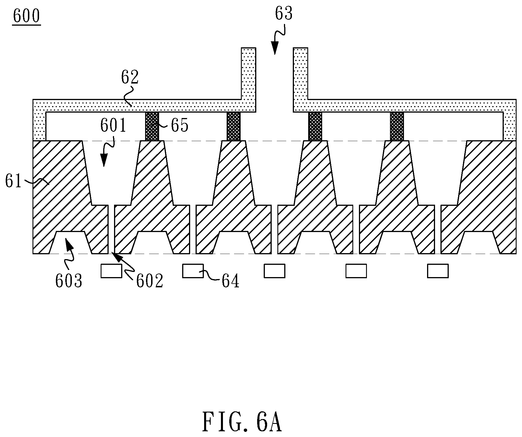
FIG. 6A shows a cross-sectional view of vacuum suction apparatus 600 according to a third embodiment of the present invention. The vacuum suction apparatus 600 of the embodiment may be adaptable to picking up miniature devices such as microLEDs.
In the embodiment, the vacuum suction apparatus 600 may include a semiconductor substrate 61 such as a silicon wafer. The vacuum suction apparatus 600 as shown in FIG. 6A may be cut from a wafer. In other examples, however, the vacuum suction apparatus 600 may be not cut from, but integrated with, a wafer. A top portion (i.e., the portion near a top surface) of the semiconductor substrate 61 may have a plurality of (first) grooves 601, which may be like the continuous grooves 101 (FIG. 1A) or the discontinuous grooves 401 (FIG. 4A). As exemplified in FIG. 6A, a bottom portion (i.e., the portion near a bottom surface) of the semiconductor substrate 61 may have a plurality of through holes 602, wherein each (first) groove 601 correspondingly connects with at least one through hole 602, and the (first) groove 601 has a width being substantially greater than a width of the through hole 602. The through holes 602 are positioned where the miniature devices are transferred. Accordingly, a pitch of the through holes 602 is equal to a pitch of transferred miniature devices. Moreover, the size of an opening of the through hole 602 at the bottom surface of the semiconductor substrate 61 is smaller than the size of the miniature device in order to ensure air tight. In one example, the diameter size of the through hole 602 is smaller than 10 micrometers, and the width of the (first) groove 601 is smaller than 100 micrometers. For brevity, only some (first) grooves 601 and through holes 602 are shown.
The vacuum suction apparatus 600 may include a vacuum cover 62, which is disposed above the semiconductor substrate 61. The vacuum cover 62 of the embodiment may, for example, include a silicon wafer, glass or sapphire. The vacuum cover 62 and the semiconductor substrate 61 construct (or define) a vacuum chamber, and an opening 63 of the vacuum cover 62 is connected to a vacuum pump (not shown). When the vacuum pump produces vacuum to cause the pressure in the vacuum chamber to be less than atmospheric pressure, miniature devices 64 can thus be sucked. Although the opening 63 is disposed at the top of the vacuum cover 62 as shown in FIG. 6A, the opening 63 may be disposed at other places in other examples.
In one embodiment, the vacuum suction apparatus 600 may include at least one post 65, disposed between a bottom surface of the vacuum cover 62 and a top surface of the semiconductor substrate 61, which is used to support the vacuum cover 62 in order to prevent collapse of the vacuum cover 62 while producing vacuum.
In one embodiment, the bottom portion of the semiconductor substrate 61 may have a plurality of second grooves 603 disposed between adjacent through holes 602. When the vacuum suction apparatus 600 picks up and transfers the miniature devices 64, the second grooves 603 can prevent the bottom surface of the semiconductor substrate 61 from touching transferred miniature devices on a substrate. The second grooves 603 may be continuous grooves as shown in a bottom view of FIG. 6B, where the continuous second grooves 603 are disposed longitudinally and/or laterally at the bottom portion of the semiconductor substrate 61. The second grooves 603 may be discontinuous grooves as shown in a bottom view of FIG. 6C, wherein the discontinuous second grooves 603 are disposed in matrix form at the bottom portion of the semiconductor substrate 61.
The first grooves 601, the second grooves 603 and the through holes 602 may be made by conventional semiconductor process or microfabrication such as anisotropic etching with an etch rate depending on a crystal face. It is noted that the first grooves 601, the second grooves 603 and the through holes 602 may be made in any sequence or be made at the same time.
FIG. 6D shows a cross-sectional view of vacuum suction apparatus 600 according to a modified third embodiment of the present invention. In the embodiment, a buffer layer 66 is formed, for example, by coating, on the bottom surface of the semiconductor substrate 61. The buffer layer 66 may include a soft (or flexible) material such as photo resist. The buffer layer 66 may have the second grooves 603 and the through holes 602 formed therein. The through hole 602 in the buffer layer 66 may have a diameter being the same as or smaller than the through hole 602 in the semiconductor substrate 61. Compared to FIG. 6A, the buffer layer 66, instead of the entire semiconductor substrate 61, may be easily replaced when the through holes 602 are blocked.
The second grooves 603 may be adaptable to the first embodiment of the present invention. FIG. 7A shows a cross-sectional lateral view of the first embodiment of the present invention, where the second grooves 603 are disposed between adjacent through holes 102, and the second groove 603 may have a width greater than the width of the miniature device. The second grooves 603 may be continuous grooves disposed at the bottom portion of the semiconductor substrate 11 with a bottom view similar to FIG. 6B. The second grooves 603 may be discontinuous grooves, arranged in matrix form, disposed at the bottom portion of the semiconductor substrate 11 with a bottom view similar to FIG. 6C. FIG. 7B shows a cross-sectional lateral view of a modified first embodiment of the present invention, where a buffer 66 is formed on the bottom surface of the semiconductor substrate 11. The buffer layer 66 may have the second grooves 603 and the through holes 102 formed therein.
The second grooves 603 may be adaptable to the second embodiment of the present invention. FIG. 8A shows a cross-sectional lateral view of the second embodiment of the present invention, where the second grooves 603 are disposed between adjacent through holes 402, and the second groove 603 may have a width greater than the width of the miniature device. The second grooves 603 may be continuous grooves disposed at the bottom portion of the semiconductor substrate 41 with a bottom view similar to FIG. 6B. The second grooves 603 may be discontinuous grooves, arranged in matrix form, disposed at the bottom portion of the semiconductor substrate 41 with a bottom view similar to FIG. 6C. FIG. 8B shows a cross-sectional lateral view of a modified first embodiment of the present invention, where a buffer 66 is formed on the bottom surface of the semiconductor substrate 41. The buffer layer 66 may have the second grooves 603 and the through holes 402 formed therein.
Although specific embodiments have been illustrated and described, it will be appreciated by those skilled in the art that various modifications may be made without departing from the scope of the present invention, which is intended to be limited solely by the appended claims.
* * * * *
D00000
D00001
D00002
D00003
D00004
D00005
D00006
D00007
D00008
D00009
D00010
D00011
XML
uspto.report is an independent third-party trademark research tool that is not affiliated, endorsed, or sponsored by the United States Patent and Trademark Office (USPTO) or any other governmental organization. The information provided by uspto.report is based on publicly available data at the time of writing and is intended for informational purposes only.
While we strive to provide accurate and up-to-date information, we do not guarantee the accuracy, completeness, reliability, or suitability of the information displayed on this site. The use of this site is at your own risk. Any reliance you place on such information is therefore strictly at your own risk.
All official trademark data, including owner information, should be verified by visiting the official USPTO website at www.uspto.gov. This site is not intended to replace professional legal advice and should not be used as a substitute for consulting with a legal professional who is knowledgeable about trademark law.