Information processing apparatus, ising device, and information processing apparatus control method
Thach , et al. April 6, 2
U.S. patent number 10,970,361 [Application Number 15/615,868] was granted by the patent office on 2021-04-06 for information processing apparatus, ising device, and information processing apparatus control method. This patent grant is currently assigned to FUJITSU LIMITED. The grantee listed for this patent is FUJITSU LIMITED. Invention is credited to Hirotaka Tamura, David Thach, Sanroku Tsukamoto.


View All Diagrams
| United States Patent | 10,970,361 |
| Thach , et al. | April 6, 2021 |
Information processing apparatus, ising device, and information processing apparatus control method
Abstract
Arithmetic circuits calculate d-1 energy values (h.sub.i2 to h.sub.id) indicating energies generated by 2-body to d-body coupling on the basis of a plurality of weight values indicating strength of 2-body to d-body coupling of 2 to d neurons including a first neuron whose output value is allowed to be updated and n-bit output values of n neurons. An adder circuit calculates a sum of these values, and a comparator circuit compares a value based on a sum of the sum and a noise value with a threshold, to determine the output value of the first neuron. An update circuit outputs n-bit updated output values in which one bit has been updated on the basis of a selection signal and the output value of the first neuron. The holding circuit holds the updated output values and outputs the updated output values as the n-bit output values used by the arithmetic circuits.
| Inventors: | Thach; David (Meguro, JP), Tamura; Hirotaka (Yokohama, JP), Tsukamoto; Sanroku (Setagaya, JP) | ||||||||||
|---|---|---|---|---|---|---|---|---|---|---|---|
| Applicant: |
|
||||||||||
| Assignee: | FUJITSU LIMITED (Kawasaki,
JP) |
||||||||||
| Family ID: | 1000005470290 | ||||||||||
| Appl. No.: | 15/615,868 | ||||||||||
| Filed: | June 7, 2017 |
Prior Publication Data
| Document Identifier | Publication Date | |
|---|---|---|
| US 20170364477 A1 | Dec 21, 2017 | |
Foreign Application Priority Data
| Jun 17, 2016 [JP] | JP2016-120717 | |||
| Current U.S. Class: | 1/1 |
| Current CPC Class: | G06N 3/063 (20130101); G06F 17/11 (20130101); G06F 13/20 (20130101); G06F 7/588 (20130101); G06N 3/0445 (20130101); G06F 30/20 (20200101); G06N 5/003 (20130101); G06N 3/0472 (20130101); G06N 7/005 (20130101); G06N 7/046 (20130101) |
| Current International Class: | G06F 17/11 (20060101); G06N 3/063 (20060101); G06N 3/04 (20060101); G06F 13/20 (20060101); G06N 5/00 (20060101); G06F 7/58 (20060101); G06F 30/20 (20200101); G06N 7/00 (20060101); G06N 7/04 (20060101) |
References Cited [Referenced By]
U.S. Patent Documents
| 5293457 | March 1994 | Arima |
| 5581659 | December 1996 | Takatori |
| 2013/0135439 | May 2013 | Kakuko |
| 2016/0064053 | March 2016 | Yamaoka |
| 2016/0065210 | March 2016 | Yoshimura |
| 2017/0061326 | March 2017 | Talathi |
| 2017/0351949 | December 2017 | Matsubara |
| 2018/0247691 | August 2018 | Okuyama |
| 2019/0155330 | May 2019 | Yamaoka |
| 7-200512 | Aug 1995 | JP | |||
Other References
|
Graf, Hans Peter, E. Sackinger, and Lawrence D. Jackel. "Recent developments of electronic neural nets in North America." Journal of VLSI signal processing systems for signal, image and video technology 6.1 (1993): 19-31. (Year: 1993). cited by examiner . Roudi, Yasser, Joanna Tyrcha, and John Hertz. "Ising model for neural data: model quality and approximate methods for extracting functional connectivity." Physical Review E 79.5 (2009): 051915. (Year: 2009). cited by examiner . Honkela, Timo, et al., eds. Artificial Neural Networks and Machine Learning--ICANN 2011: 21st International Conference on Artificial Neural Networks, Espoo, Finland, Jun. 14-17, 2011, Proceedings. vol. 6792. Springer, 2011: I-390. (Year: 2011). cited by examiner . Sathasivam, Saratha. "Boltzmann machine and new activation function comparison." Applied Mathematical Sciences 5.78 (2011): 3853-3860. (Year: 2011). cited by examiner . Ravanbakhsh, Siamak, Russell Greiner, and Brendan Frey. "Training restricted boltzmann machine by perturbation." arXiv preprint arXiv:1405.1436 (2014). (Year: 2014). cited by examiner . Zhao, Zhi-jin, and Jia-wei Gu. "Recognition of digital modulation signals based on hybrid three-order restricted Boltzmann machine." 2015 IEEE 16th International Conference on Communication Technology (ICCT). IEEE, 2015: 166-169 (Year: 2015). cited by examiner . C. R. Schneider et al., "Analog CMOS Deterministic Boltzmann Circuits", IEEE Journal of Solid-State Circuits, vol. 28, No. 8, Aug. 1993, pp. 907-914 (8 pages). cited by applicant . R. Babbush et al., "Resource Efficient Gadgets for Compiling Adiabatic Quantum Optimization Problems", arXiv:1307.8041v1, [quant-ph], Jul. 31, 2013 (11 pages). cited by applicant . V. S. Denchev et al., "What is the Computational Value of Finite Range Tunneling?", arXiv:1512.02206v4, [quant-ph], Jan. 26, 2016 (17 pages). cited by applicant . A. DeGloria et al., "Efficient Implementation of the Boltzmann Machine Algorithm", IEEE Transactions on Neural Networks, vol. 4, No. 1, Jan. 1993, pp. 159-163 (5 pages). cited by applicant. |
Primary Examiner: Afshar; Kamran
Assistant Examiner: Baldwin; Randall K.
Attorney, Agent or Firm: Fujitsu Patent Center
Claims
What is claimed is:
1. An information processing apparatus comprising: an ising device; and a control device, wherein the ising device includes: a random signal generation circuit that outputs, a plurality of times, a selection signal for randomly selecting a first neuron whose output value is allowed to be updated from n neurons, wherein n is a natural number of 3 or more, d-1 arithmetic circuits that calculate, based on a plurality of weight values indicating strength of each coupling from 2-body coupling to d-body coupling of two to d neurons including the first neuron selected from the n neurons based on the selection signal and n-bit output values of the n neurons, d-1 energy values for the first neuron indicating energies generated by the respective 2-body to d-body coupling of the two to d neurons including the first neuron or change amounts of the d-1 energy values for the first neuron, wherein d is a natural number not less than 3 and not more than n, an adder circuit that calculates a first sum by adding up the d-1 energy values or calculates a second sum by adding up the change amounts of the d-1 energy values and outputs the first sum or the second sum, a comparator circuit that determines and outputs a first output value of the first neuron, based on a first comparison result obtained by comparing a first value based on a sum of the first sum and a noise value with a threshold or based on a second comparison result obtained by comparing a third value with the threshold, the third value being based on a sum of a second value that indicates a sum of the energies generated by the respective 2-body to d-body coupling and that is updated based on the second sum and the noise value, an update circuit that outputs n-bit updated output values in which one bit has been updated based on the selection signal and the first output value, and a holding circuit that holds the n-bit updated output values and outputs the n-bit updated output values as the n-bit output values used by the arithmetic circuits, and wherein the control device controls a noise width of the noise value.
2. The information processing apparatus according to claim 1, wherein each of the d-1 arithmetic circuits includes a storage unit, and wherein the control device determines a number of weight values stored in the storage unit in accordance with symmetry of the weight values.
3. The information processing apparatus according to claim 2, wherein the control device sets the number of weight values stored in the storage unit, based on n.sup.d-3.times.(n.sup.2-n)/2.
4. An ising device comprising: a random signal generation circuit that outputs, a plurality of times, a selection signal for randomly selecting a first neuron whose output value is allowed to be updated from n neurons, wherein n is a natural number of 3 or more; d-1 arithmetic circuits that calculate, based on a plurality of weight values indicating strength of each coupling from 2-body coupling to d-body coupling of two to d neurons including the first neuron selected from the n neurons based on the selection signal and n-bit output values of the n neurons, d-1 energy values for the first neuron indicating energies generated by the respective 2-body to d-body coupling of the two to d neurons including the first neuron or change amounts of the d-1 energy values for the first neuron, wherein d is a natural number not less than 3 and not more than n; an adder circuit that calculates a first sum by adding up the d-1 energy values or calculates a second sum by adding up the change amounts of the d-1 energy values and outputs the first sum or the second sum; a comparator circuit that determines and outputs a first output value of the first neuron, based on a first comparison result obtained by comparing a first value based on a sum of the first sum and a noise value with a threshold or based on a second comparison result obtained by comparing a third value with the threshold, the third value being based on a sum of a second value that indicates a sum of the energies generated by the respective 2-body to d-body coupling and that is updated based on the second sum and the noise value; an update circuit that outputs n-bit updated output values in which one bit has been updated based on the selection signal and the first output value; and a holding circuit that holds the n-bit updated output values and outputs the n-bit updated output values as the n-bit output values used by the arithmetic circuits.
5. An information processing apparatus control method comprising: preparing an ising device including: a random signal generation circuit that outputs, a plurality of times, a selection signal for randomly selecting a first neuron whose output value is allowed to be updated from n neurons, wherein n is a natural number of 3 or more, d-1 arithmetic circuits that calculate, based on a plurality of weight values indicating strength of each coupling from 2-body coupling to d-body coupling of two to d neurons including the first neuron selected from the n neurons based on the selection signal and n-bit output values of the n neurons, d-1 energy values for the first neuron indicating energies generated by the respective 2-body to d-body coupling of the two to d neurons including the first neuron or change amounts of the d-1 energy values for the first neuron, wherein d is a natural number not less than 3 and not more than n, an adder circuit that calculates a first sum by adding up the d-1 energy values or calculates a second sum by adding up the change amounts of the d-1 energy values and outputs the first sum or the second sum, a comparator circuit that determines and outputs a first output value of the first neuron, based on a first comparison result obtained by comparing a first value based on a sum of the first sum and a noise value with a threshold or based on a second comparison result obtained by comparing a third value with the threshold, the third value being based on a sum of a second value that indicates a sum of the energies generated by the respective 2-body to d-body coupling and that is updated based on the second sum and the noise value, an update circuit that outputs n-bit updated output values in which one bit has been updated based on the selection signal and the first output value, and a holding circuit that holds the n-bit updated output values and outputs the n-bit updated output values as the n-bit output values used by the arithmetic circuits; causing a control device to set a plurality of weight values in the ising device; and causing the control device to control a noise width of the noise value.
6. The information processing apparatus according to claim 1, wherein the update circuit outputs the n-bit updated output values of the n neurons in which one bit, among the n-bit output values of the n neurons, has been updated based on the selection signal and the first output value.
Description
CROSS-REFERENCE TO RELATED APPLICATION
This application is based upon and claims the benefit of priority of the prior Japanese Patent Application No. 2016-120717, filed on Jun. 17, 2016, the entire contents of which are incorporated herein by reference.
FIELD
The embodiments discussed herein relate to an information processing apparatus, an ising device, and an information processing apparatus control method.
BACKGROUND
Neumann computers are not very suitable for solving multivariable optimization problems. However, to solve these problems, there is a method which uses an ising device (also referred to as a Boltzmann machine) that uses an ising energy function. Such an ising device performs calculation by replacing a problem to be calculated with an ising model, which is a model representing the behavior of a ferromagnetic spin.
An ising device can be modeled by using a neural network. In such cases, each of the units (bits) included in the ising device functions as a neuron that outputs 0 or 1 on the basis of states of the other bits and weight values (also referred to as coupling coefficients) each of which indicates coupling strength between the corresponding bit and one of the other bits. For example, the ising device performs simulated annealing to obtain, as a solution, a combination of bit states from which a minimum value of the above energy function (also referred to as a cost function, an objective function, etc.) is obtained.
To shorten the calculation time, realizing such an ising device with hardware modules has conventionally been proposed.
A conventional ising device uses an energy function (which will hereinafter be referred to as a second-order energy function) including a weight value of coupling strength between two bits. One possible way to apply an ising device to more variety of optimization problems is to use an energy function (which will hereinafter be referred to as a high-order energy function) including weight values indicating mutual coupling strength among three or more bits.
There has been proposed a method for solving an optimization problem using a high-order energy function. In this method, an optimization problem using a high-order energy function is solved by converting the optimization problem into an optimization problem using a plurality of second-order energy functions.
Japanese Laid-open Patent Publication No. 07-200512, Aug. 4, 2015
C. R. Schneider and H. C. Card, "Analog CMOS Deterministic Boltzmann Circuits", IEEE Journal of Solid-State Circuits, VOL. 28, No. 8, pp. 907-914, August 1993
R. Babbush, B. O'Gorman, and A. Aspuru-Guzik, "Resource Efficient Gadgets for Compiling Adiabatic Quantum Optimization Problems", arXiv: 1307.8041v1, [quant-ph], Jul. 31, 2013
V. S. Denchev, S. Boixo, S. V. Isakov, N. Ding, R. Babbush, V. Smelyanskiy, J. Martinis, and H. Neven, "What is the Computational Value of Finite Range Tunneling?", arXiv: 1512.02206v4, [quant-ph], Jan. 26, 2016
However, when converting an optimization problem using a high-order energy function into an optimization problem using second-order energy functions, "ancillary bit" has conventionally been introduced. Addition of this ancillary bit could slow down the convergence into an optimal solution or decrease the number of usable bits in simulated annealing.
SUMMARY
According to one aspect, there is provided an information processing apparatus including: an ising device; and a control device, wherein the ising device includes: a random signal generation circuit that outputs, a plurality of times, a selection signal for randomly selecting a first neuron whose output value is allowed to be updated from n neurons, wherein n is a natural number of 3 or more, d-1 arithmetic circuits that calculate, based on a plurality of weight values indicating strength of 2-body coupling to d-body coupling of two to d neurons including the first neuron selected from the n neurons based on the selection signal and n-bit output values of the n neurons, d-1 energy values indicating energies generated by the respective 2-body to d-body coupling or change amounts of the d-1 energy values, wherein d is a natural number not less than 3 and not more than n, an adder circuit that calculates a first sum by adding up the d-1 energy values or calculates a second sum by adding up the change amounts of the d-1 energy values and outputs the first sum or the second sum, a comparator circuit that determines and outputs a first output value of the first neuron, based on a first comparison result obtained by comparing a first value based on a sum of the first sum and a noise value with a threshold or based on a second comparison result obtained by comparing a third value with the threshold, the third value being based on a sum of a second value that indicates a sum of the energies generated by the respective 2-body to d-body coupling and that is updated based on the second sum and the noise value, an update circuit that outputs n-bit updated output values in which one bit has been updated based on the selection signal and the first output value, and a holding circuit that holds the n-bit updated output values and outputs the n-bit updated output values as the n-bit output values used by the arithmetic circuits, and wherein the control device controls a noise width of the noise value.
The object and advantages of the invention will be realized and attained by means of the elements and combinations particularly pointed out in the claims.
It is to be understood that both the foregoing general description and the following detailed description are exemplary and explanatory and are not restrictive of the invention.
BRIEF DESCRIPTION OF DRAWINGS
FIG. 1 illustrates an example of an information processing apparatus according to a first embodiment;
FIG. 2 illustrates an example of an arithmetic circuit that calculates a local field value generated by d-body coupling;
FIG. 3 illustrates examples of an update circuit and a holding circuit;
FIG. 4 illustrates an example of an ising device in which an optimization problem using a third-order energy function is mapped;
FIG. 5 illustrates an example of an arithmetic circuit that calculates a local field value generated by 2-body coupling;
FIG. 6 illustrates an example of an arithmetic circuit that calculates a local field value generated by 3-body coupling;
FIG. 7 is a flowchart illustrating an example of an operation of the information processing apparatus;
FIG. 8 is a flowchart illustrating an example of simulated annealing;
FIG. 9 illustrates progress of simulated annealing;
FIG. 10 illustrates examples of weight values indicating 2-body coupling;
FIG. 11 illustrates examples of weight values indicating 3-body coupling;
FIG. 12 illustrates examples of weight values indicating 3-body coupling when the number of neurons is n;
FIG. 13 illustrates examples of weight values indicating 4-body coupling when the number of neurons is n;
FIG. 14 is a flowchart illustrating an example of weight value list generation processing;
FIG. 15 illustrates an example of a weight value list;
FIG. 16 illustrates an example of an information processing apparatus according to a second embodiment;
FIG. 17 illustrates an example of a circuit unit;
FIG. 18 illustrates an example of an arithmetic circuit that calculates a change amount of a local field value generated by 2-body coupling;
FIG. 19 illustrates an example of an arithmetic circuit that calculates a change amount of a local field value generated by 3-body coupling;
FIG. 20 illustrates an example of a two-output-value selector circuit; and
FIG. 21 is a flowchart illustrating an example of simulated annealing performed by the information processing apparatus according to the second embodiment.
DESCRIPTION OF EMBODIMENTS
Hereinafter, embodiments will be described with reference to the accompanying drawings, wherein like reference characters refer to like elements throughout.
First Embodiment
FIG. 1 illustrates an example of an information processing apparatus 1 according to a first embodiment.
The information processing apparatus 1 includes an ising device 2, a control device 3, and a memory 4. The control device 3 maps an optimization problem using a high-order (d.gtoreq.3) energy function in the ising device 2. In addition, the ising device 2 according to the first embodiment functions as a neural network including n neurons (n is a natural number of 3 or more).
The ising device 2 includes a random signal generation circuit 10, arithmetic circuits 11a1 to 11a(d-1), an adder circuit 12, a comparator circuit 13, an update circuit 14, a holding circuit 15, a bias value holding circuit 16, and a noise generation circuit 17. For example, the ising device 2 is realized by a single semiconductor integrated circuit (a single chip).
The random signal generation circuit 10 outputs a selection signal for randomly selecting a neuron whose output value is allowed to be updated from the n neurons a plurality of times. For example, each of the n neurons is given a different identification number (which will hereinafter be referred to as a neuron ID). In FIG. 1, the random signal generation circuit 10 outputs a selection signal that specifies i (1.ltoreq.i.ltoreq.n) as a neuron ID. For example, the random signal generation circuit 10 includes linear feedback shift registers (LFSRs).
The d-1 arithmetic circuits 11a1 to 11a(d-1) (d is a natural number not less than 3 and not more than n) receive the selection signal outputted by the random signal generation circuit 10 and n-bit output values x.sub.1 to x.sub.n of the n neurons outputted by the holding circuit 15. In addition, the arithmetic circuit 11a1 to 11a(d-1) calculate d-1 energy values h.sub.i2 to h.sub.id on the basis of a plurality of weight values indicating strength of 2-body coupling to d-body coupling of two to d neurons including the neuron selected by the selection signal and the output values x.sub.1 to x.sub.n. The energy values will hereinafter be referred to as local field values. The local field values h.sub.i2 to h.sub.id indicate energies generated by the respective 2-body coupling to d-body coupling.
For example, the control device 3 sets these weight values indicating strength of 2-body coupling to d-body coupling (which will simply be referred to as weight values indicating 2-body coupling to d-body coupling) on the basis of the problem to be calculated and stores the weight values in storage units (for example, registers) in the arithmetic circuit 11a1 to 11a(d-1). FIG. 1 illustrates examples of weight values indicating 2-body coupling, 3-body coupling, and 4-body coupling when n=1 neurons. For example, the weight value of 2-body coupling of neurons 20 and 21 whose neuron IDs are i and k, respectively, is denoted by W.sub.ik. In addition, the weight value of 2-body coupling of the neuron 21 and a neuron 22 whose neuron IDs are k and j, respectively, is denoted by W.sub.jk. In addition, the weight value of 2-body coupling of the neurons 20 and 22 whose neuron IDs are i and j, respectively, is denoted by W.sub.ij. In addition, the weight value of 3-body coupling of the neurons 20 to 22 whose neuron IDs are i, j, and k, respectively, is denoted by W.sub.ijk. In addition, the weight value of 4-body coupling of the neurons 20 to 22 and a neuron 23 whose neuron IDs are j, k, and l, respectively, is denoted by W.sub.ijkl.
The adder circuit 12 adds up the local field values h.sub.i2 to h.sub.id and outputs a sum of these values.
The comparator circuit 13 adds up the sum obtained by the adder circuit 12, a noise value, and a bias value and compares a sum of these values with a threshold (for example, 0). On the basis of the comparison result, the comparator circuit 13 determines and outputs the output value of the neuron selected by the selection signal. For example, the comparator circuit 13 includes an adder circuit that adds up the sum obtained by the adder circuit 12, the noise value, and the bias value. Hereinafter, a value (energy value) obtained by adding up the sum obtained by the adder circuit 12 and the bias value will be referred to as a local field value h.sub.i.
For example, when the sum of the local field value h.sub.i and the noise value is negative, the comparator circuit 13 outputs 1. When the sum of the local field value h.sub.i and the noise value is positive, the comparator circuit 13 outputs 0. The bias value may be 0.
The update circuit 14 outputs n-bit updated output values of the n neurons in which one bit has been updated on the basis of the selection signal and the output value outputted by the comparator circuit 13. For example, when the output value of a neuron whose neuron ID is i outputted by the comparator circuit 13 is different from the previous value, the update circuit 14 outputs n-bit updated output values in which the i-th bit has been updated. When the output value of the neuron whose neuron ID is i outputted by the comparator circuit 13 is the same as the previous value, the update circuit 14 may output no updated output values.
The holding circuit 15 holds the updated output values outputted by the update circuit 14 and outputs the updated output values as the n-bit output values of the n neurons used by the arithmetic circuits 11a1 to 11a(d-1) in synchronization with a clock signal clk. The holding circuit 15 is realized by a plurality of flip flops, for example. The clock signal clk is supplied by the control device 3, for example. The clock signal clk may be supplied by a clock signal generation circuit (not illustrated) arranged outside or inside the ising device 2.
For example, the bias value holding circuit 16 is a register or a flash memory and holds a bias value for each of the n neurons. In addition, the bias value holding circuit 16 supplies the bias value of a neuron specified by the selection signal outputted by the random signal generation circuit 10 to the comparator circuit 13, for example. For example, the control device 3 sets the bias values in advance on the basis of the problem to be calculated.
The noise generation circuit 17 outputs a noise value for performing simulated annealing on the basis of an instruction from the control device 3. For example, as is the case with the random signal generation circuit 10, the noise generation circuit 17 may also be configured by using LFSRs. In addition, for example, the noise generation circuit 17 includes an amplifier circuit. For example, the control device 3 changes the amplification factor of the amplifier circuit, to control the amplitude of the noise value.
The control device 3 controls the random signal generation circuit 10 and the noise generation circuit 17 to control the noise width. For example, to perform simulated annealing, the control device 3 controls the amplifier circuit included in the noise generation circuit 17 and gradually drops the noise width of the noise value (the amplitude of the noise). In addition, the control device 3 previously sets a plurality of weight values and a plurality of bias values on the basis of the optimization problem to be calculated. In addition, the control device 3 performs mapping by writing the plurality of weight values in registers in the arithmetic circuits 11a1 to 11a(d-1) via buses (not illustrated) and writing the plurality of bias values in the bias value holding circuit 16.
For example, the control device 3 may be realized by a processor. Examples of the processor include a central processing unit (CPU), a micro processing unit (MPU), a digital signal processor (DSP), an application specific integrated circuit (ASIC), and a programmable logic device (PLD). The processor may be a combination of at least two of a CPU, an MPU, a DSP, an ASIC, and a PLD. The control device 3 may be a personal computer (PC), a server computer, or the like.
For example, when the control device 3 is a processor, the memory 4 is a non-volatile storage device that holds an operating system (OS), middleware, software programs such as application software programs, and data executed by the processor. The memory 4 may hold a program for generating weight value lists, which will be described below. Examples of the non-volatile storage device include a flash memory, a solid state drive (SSD), and a hard disk drive (HDD).
The above information processing apparatus 1 realizes operations of the ising energy function by using hardware modules. For example, a high-order energy function E(x) is defined by the following expression (1).
.function..times..times..times..times..times..times..times..times..times.- .times..times..times..times..times..times..times. ##EQU00001##
The first term on the right side of expression (1) is directed to all the combinations of two neurons selectable from all the neurons without missing any neuron or redundantly counting any neuron. More specifically, the first term represents the sum of products, each of which is obtained by multiplying the output values of two neurons and a weight value of the corresponding 2-body coupling by each other. The second term on the right side of expression (1) represents the sum of products, each of which is obtained by multiplying the bias value by the output value per neuron. In expression (1), b.sub.i represents the bias value of the neuron whose neuron ID is i. The third term on the right side of expression (1) is directed to all the combinations of three neurons selectable from all the neurons without missing any neuron or redundantly counting any neuron. More specifically, the third term represents the sum of products, each of which is obtained by multiplying the output values of three neurons and a weight value of the corresponding 3-body coupling by each other. The fourth term on the right side of expression (1) is directed to all the combinations of four neurons selectable from all the neurons without missing any neuron or redundantly counting any neuron. More specifically, the fourth term represents the sum of products, each of which is obtained by multiplying the output values of four neurons and a weight value of the corresponding 4-body coupling by each other.
In this ising energy function, the change of the energy value when the output value of a neuron changes from 1 to 0 or from 0 to 1 is determined by the weight values, each of which indicates coupling between the neuron and one of the other neurons, and the output values of the neurons.
For example, when the output value of a neuron whose neuron ID is i has changed, the change of the energy is expressed by the following expression (2).
.DELTA..times..times..times..times..times..times..times..times..times..ti- mes..times..times..times..times. ##EQU00002##
In expression (2), when x.sub.i is 1, 2x.sub.i-1 is 1, and when x.sub.i is 0, 2x.sub.i-1 is -1. In addition, the local field value h.sub.i that indicates the energy generated by coupling of neurons including the neuron whose neuron ID is i in expression (2) may be expressed by the following expression (3).
.times..times..times..times..times..times..times..times..times. ##EQU00003##
The second term on the right side of expression (3) represents the energy generated by 2-body coupling of neurons including the neuron whose neuron ID is i. The third term on the right side represents the energy generated by 3-body coupling of neurons including the neuron whose neuron ID is i. W.sub.ijk is a weight value of 3-body coupling of neurons whose neuron IDs are i, j, and k, respectively, of all the n neurons. In addition, the fourth term on the right side represents the energy generated by 4-body coupling of neurons including the neuron whose neuron ID is i. W.sub.ijkl is a weight value of 4-body coupling of neurons whose neuron IDs are i, j, k, and l, respectively, of all the n neurons.
As is clear from expressions (2) and (3), when the local field value h.sub.i is negative and 2x.sub.i-1 is positive or when the local field value h.sub.i is positive and 2x.sub.i-1 is negative, .DELTA.E.sub.i is negative, i.e., the energy drops.
The arithmetic circuits 11a1 to 11a(d-1) illustrated in FIG. 1 calculate the local field value h.sub.i2 to h.sub.id that indicate the energies generated by the respective 2-body coupling to d-body coupling.
For example, the arithmetic circuit 11a1 calculates the local field value h.sub.i2 corresponding to the second term on the right side of expression (3), and the arithmetic circuit 11a2 calculates the local field value h.sub.i3 corresponding to the third term of expression (3).
(Example of Arithmetic Circuit)
FIG. 2 illustrates an example of an arithmetic circuit that calculates a local field value generated by d-body coupling.
The arithmetic circuit 11a(d-1) includes registers 30a1 to 30an, a selector circuit 31, a multiplier unit 32, and an adder unit 33.
The registers 30a1 to 30an hold a plurality of weight values of d-body coupling of d neurons. For example, the register 30a1 holds a plurality of weight values of d-body coupling of the d neurons including a neuron whose neuron ID is 1. The register 30a2 holds a plurality of weight values of d-body coupling of the d neurons including a neuron whose neuron ID is 2. In addition, the register 30an holds a plurality of weight values of d-body coupling of the d neurons including a neuron whose neuron ID is n.
The selector circuit 31 outputs a plurality of weight values stored in one of the registers 30a1 to 30an on the basis of the selection signal outputted by the random signal generation circuit 10. For example, when the selector circuit 31 receives a selection signal that specifies the neuron whose neuron ID is 1, the selector circuit 31 outputs a plurality of weight values stored in the register 30a1.
The multiplier unit 32 and the adder unit 33 calculate the energy (the local field value h.sub.id) generated by d-body coupling, the energy being a part of the local field value h.sub.i expressed by the expression (3), on the basis of the output values x.sub.1 to x.sub.n and the plurality of weight values outputted by the selector circuit 31. The multiplier unit 32 includes m multiplier circuits 32a1 to 32am, and the adder unit 33 includes p adder circuits 33a1 to 33ap. The number of multiplier circuits 32a1 to 32am and the number of adder circuits 33a1 to 33ap will be described below.
(Example of Update Circuit and Holding Circuit)
FIG. 3 illustrates examples of the update circuit 14 and the holding circuit 15.
The update circuit 14 includes a multiplexer 14a and selector circuits 14b1 to 14bn. The holding circuit 15 includes flip flops 15a1 to 15an.
The multiplexer 14a generates a selection signal supplied to the selector circuit 14b1 to 14bn on the basis of the selection signal outputted by the random signal generation circuit 10. For example, when the multiplexer 14a receives a selection signal for selecting one of the n neurons, the multiplexer 14a supplies 1 as a selection signal to one of the selector circuits 14b1 to 14bn that corresponds to the selected neuron. The multiplexer 14a supplies 0 to the other selector circuits. For example, when the multiplexer 14a receives a selection signal that specifies the neuron whose neuron ID is 1, the multiplexer 14a supplies 1 as the selection signal to the selector circuit 14b1 and supplies 0 as the selection signal to the selector circuits 14b2 to 14bn.
The n selector circuits 14b1 to 14bn are arranged to correspond to the n neurons. Each of the selector circuits 14b1 to 14bn has two input terminals. One of the input terminals of a selector circuit is connected to the output terminal of a corresponding one of the flip flops 15a1 to 15an, and the other input terminal is connected to the output terminal of the comparator circuit 13. When any one of the selector circuits 14b1 to 14bn receives 1 as the selection signal from the multiplexer 14a, this selector circuit selects and outputs the output value of the neuron outputted by the comparator circuit 13. When any one of the selector circuits 14b1 to 14bn receives 0 as the selection signal from the multiplexer 14a, this selector circuit selects and outputs a value outputted by the corresponding one of the flip flops 15a1 to 15an.
The flip flops 15a1 to 15an in the holding circuit 15 captures and outputs the values (n-bit updated output values) outputted by the selector circuits 14b1 to 14bn in synchronization with the clock signal clk.
For example, when the random signal generation circuit 10 outputs a selection signal that specifies the neuron whose neuron ID is 1, the selector circuit 14b1 selects and outputs the output value of the neuron outputted by the comparator circuit 13. The selector circuits 14b2 to 14bn select and output the values outputted by the respective flip flops 15a2 to 15an. In this way, the holding circuit 15 outputs n-bit output values in which only the bit value corresponding to the neuron whose neuron ID is 1 has been updated.
(Example of Ising Device in which Optimization Problem Using Third-Order Energy Function is Mapped)
FIG. 4 illustrates an example of an ising device 2a in which an optimization problem using a third-order energy function is mapped. In FIGS. 1 and 4, like reference characters refer to like elements.
The ising device 2a in which an optimization problem using a third-order energy function is mapped includes the two arithmetic circuits 11a1 and 11a2. The arithmetic circuit 11a1 calculates the local field value h.sub.i2, which is the energy generated by 2-body coupling of two neurons including the neuron whose neuron ID is i. The arithmetic circuit 11a2 calculates the local field value h.sub.i3, which is the energy generated by 3-body coupling of three neurons including the neuron whose neuron ID is i.
An adder circuit 12a outputs a sum of the two local field values h.sub.i2 and h.sub.i3.
FIG. 5 illustrates an example of the arithmetic circuit 11a1 that calculates a local field value generated by 2-body coupling.
The arithmetic circuit 11a1 includes registers 40a1 to 40an, a selector circuit 41, a multiplier unit 42, and an adder unit 43.
The registers 40a1 to 40an hold a plurality of weight values, each of which indicates 2-body coupling of two neurons. For example, the register 40a1 holds weight values W.sub.12 to W.sub.1n, each of which indicates 2-body coupling of two neurons including the neuron whose neuron ID is 1. The register 40a2 holds a plurality of weight values W.sub.21 and W.sub.23 to W.sub.2n each of which indicates 2-body coupling of two neurons including the neuron whose neuron ID is 2. In addition, the register 40an holds weight values W.sub.n1 to W.sub.n(n-1), each of which indicates 2-body coupling of two neurons including a neuron whose neuron ID is n.
The selector circuit 41 outputs a plurality of weight values stored in one of the registers 40a1 to 40an on the basis of the selection signal outputted by the random signal generation circuit 10.
The multiplier unit 42 includes n multiplier circuits 42a1 to 42an, and the adder unit 43 includes q adder circuits 43a1 to 43aq. The multiplier unit 42 and the adder unit 43 calculate the energy (the local field value h.sub.i2) generated by 2-body coupling, the energy being a part of the local field value h.sub.i expressed by the expression (3), on the basis of the output values x.sub.1 to x.sub.n and the plurality of weight values outputted by the selector circuit 41.
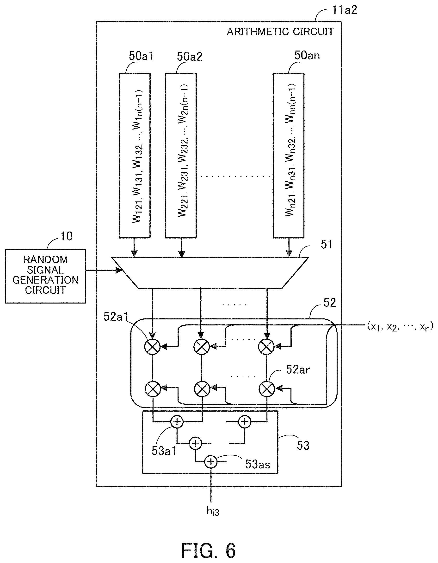
FIG. 6 illustrates an example of the arithmetic circuit 11a2 that calculates a local field value generated by 3-body coupling.
The arithmetic circuit 11a2 includes registers 50a1 to 50an, a selector circuit 51, a multiplier unit 52, and an adder unit 53.
The register 50a1 to 50an hold a plurality of weight values, each of which indicates 3-body coupling of three neurons. For example, the register 50a1 holds weight values W.sub.121, W.sub.131, W.sub.132, . . . , and W.sub.1n(n-1), each of which indicates 3-body coupling of three neurons including the neuron whose neuron ID is 1. The register 50a2 holds a plurality of weight values W.sub.221, W.sub.231, W.sub.232, . . . , and W.sub.2n(n-1), each of which indicates 3-body coupling of three neurons including the neuron whose neuron ID is 2. In addition, the register 50an holds weight values W.sub.n21, W.sub.n31, W.sub.n32, . . . , and W.sub.nn(n-1), each of which indicates 3-body coupling of three neurons including the neuron whose neuron ID is n.
The selector circuit 51 outputs a plurality of weight values stored in one of the registers 50a1 to 50an on the basis of the selection signal outputted by the random signal generation circuit 10.
The multiplier unit 52 includes r multiplier circuits 52a1 to 52ar, and the adder unit 53 includes s adder circuits 53a1 to 53as. The multiplier unit 52 and the adder unit 53 calculate the energy (the local field value h.sub.i3) generated by 3-body coupling, the energy being a part of the local field value h.sub.i expressed by the expression (3), on the basis of the output values x.sub.1 to x.sub.n and the plurality of weight values outputted by the selector circuit 51.
(Example of Operation of Information Processing Apparatus According to First Embodiment)
Hereinafter, an example of an operation of the information processing apparatus 1 in FIG. 1 controlled by the control device 3 will be described with reference to a flowchart.
FIG. 7 is a flowchart illustrating an example of an operation of the information processing apparatus 1.
First, the control device 3 extracts the weight values of 2-body coupling to d-body coupling stored in the memory 4, for example (step S1). This example assumes that the weight values based on the problem to be calculated are prepared in advance.
Next, the control device 3 writes the extracted weight values in registers in arithmetic circuits 11a1 to 11a(d-1) (for example, in the registers 30a1 to 30an in the case of the arithmetic circuit 11a(d-1)) (step S2). Namely, in step S2, the optimization problem is mapped. In step S2, the control device 3 may write the bias value of an individual neuron in the bias value holding circuit 16.
Next, the simulated annealing is performed, which is controlled by the control device 3 (step S3). Next, the control device 3 acquires the output values x.sub.1 to x.sub.n of the n neurons as a result of the simulated annealing. Namely, the control device 3 acquires the output values x.sub.1 to x.sub.n as a solution to the optimization problem (step S4). Next, the control device 3 ends the present processing.
FIG. 8 is a flowchart illustrating an example of simulated annealing.
First, controlled by the control device 3, the random signal generation circuit 10 outputs a selection signal for randomly selecting a neuron whose output value is allowed to be updated (a neuron whose neuron ID is i) (step S10).
Next, the arithmetic circuit 11a1 to 11a(d-1) calculate the local field values h.sub.i2 to h.sub.id that indicate the energies generated by 2-body coupling to d-body coupling, respectively (step S11). Next, the adder circuit calculates a sum of the local field values h.sub.i2 to h.sub.id (step S12).
When a sum of the local field value h.sub.i (a sum of the sum calculated by the adder circuit 12 and a bias value) and a noise value is smaller than a threshold (for example, 0) (step S13: YES), the comparator circuit 13 outputs 1 as its output value (new_x.sub.i) (step S14).
When a sum of the local field value h.sub.i and the noise value is equal to or more than the threshold (step S13: NO), the comparator circuit 13 outputs 0 as its output value (new_x.sub.i) (step S15).
After steps S14 or S15, if the output value new_x.sub.i differs from the original output value x.sub.i of the neuron whose neuron ID is i (step S16: NO), the update circuit 14 outputs n-bit updated output values in which the i-th bit has been updated (step S17). Next, the processing returns to step S10.
If the output value new_x.sub.i is the same as the original output value x.sub.i (step S16: YES), the control device 3 determines whether the output values x.sub.1 to x.sub.n (neuron states) have remained the same for a certain period (step S18). If the output values x.sub.1 to x.sub.n have remained the same for a certain period (step S18: YES), the control device 3 ends the simulated annealing.
If the output values x.sub.1 to x.sub.n have changed within the certain period (step S18: NO), the processing returns to step S10.
The simulated annealing is performed as the noise generation circuit 17 gradually drops the noise width under control of the control device 3 every time a neuron allowed to be updated is selected.
For example, the noise generation circuit 17 generates a noise value so that the probability with which the output value of the comparator circuit 13 represents 1 accords with a sigmoid function. For example, the noise generation circuit 17 generates a noise value so that a probability P.sub.i(h.sub.i) with which the output value x.sub.i of the neuron whose neuron ID is i represents 1 satisfies the following expression (4). P.sub.i(h.sub.i)=1/[1+exp(-h.sub.i/T)] (4)
In expression (4), T represents an effective temperature.
A probability density function p(ns) of a noise value ns generated to obtain the probability P.sub.i(h.sub.i) in expression (4) is expressed by the following expression (5). p(ns)=exp(-h.sub.i/T)/[1+exp(-h.sub.i/T)].sup.2 (5)
FIG. 9 illustrates progress of simulated annealing.
The vertical axis represents energy E, and the horizontal axis represents combinations q.sub.K of output values of all the neurons. The combinations q.sub.K are represented by "000 . . . 0" to "111 . . . 1". FIG. 9 illustrates how the convergence into a solution is achieved as the noise width is dropped from W1 to W3. Dropping the noise width means dropping the effective temperature T in expression (5).
When the noise width is W1, even when an individual solution reaches a local solution q.sub.k1, q.sub.k2, q.sub.k4, or q.sub.k5 (a solution when the energy represents a local minimal value), the local solution can change in the direction of higher energy. Thus, these solutions can shift from the local solutions. As the noise width gradually drops to W2 and W3, the change of the individual solution is gradually limited, and the convergence into an optimal solution q.sub.k3 (a solution when the energy represents a minimum value) is finally achieved.
In the information processing apparatus 1 and the ising device 2 according to the first embodiment, the arithmetic circuits 11a1 to 11a(d-1) calculate the energies (the local field values h.sub.i2 to h.sub.id) generated by 2-body coupling to d-body coupling of 2 to d neurons, respectively. In addition, a value based on a sum of the local field values h.sub.i2 to h.sub.id is compared with a threshold, and the output values of the neurons are determined on the basis of the comparison result.
In this way, an optimization problem using a high-order energy function is mapped in the ising device 2 without using any ancillary bit. While addition of this ancillary bit could slow down the convergence into an optimal solution or decrease the number of usable bits in simulated annealing, the ising device 2 does not have these problems.
In addition, for example, an optimization problem using a high-order energy function does not need to be converted into an optimization problem using a plurality of second-order energy functions, an optimization problem is easily mapped in the ising device 2.
Examples of such an optimization problem using a high-order energy function include a non-deterministic polynomial (NP) complete problem.
(Examples of Extraction and Writing of Weight Values)
Next, examples of steps S1 and S2 illustrated in FIG. 7 will be described.
FIG. 10 illustrates examples of weight values indicating 2-body coupling.
FIG. 10 illustrates a weight value group 60a including a plurality of weight values each of which indicates 2-body coupling when the number of neurons is 4. For example, W.sub.21 is a weight value that indicates 2-body coupling of the two neurons whose neuron IDs are 2 and 1, respectively.
With the Boltzmann machine, there are conditions that W.sub.ii=0 and W.sub.ij=W.sub.ji (i and j are each a natural number not less than 1 and not more than n). Thus, W.sub.21=W.sub.12, W.sub.31=W.sub.13, W.sub.41=W.sub.14, W.sub.42=W.sub.24, and W.sub.43=W.sub.34. In addition, each of the weight values W.sub.11, W.sub.22, W.sub.33, and W.sub.44 in a weight value group 60b in FIG. 10 is 0.
Thus, calculation may be performed without the weight values W.sub.11, W.sub.22, W.sub.33, and W.sub.44. In contrast, both weight values having a symmetry relationship such as W.sub.21 and W.sub.12 are used to calculate the local field value h.sub.i2 generated by 2-body coupling, as illustrated in FIG. 5.
FIG. 11 illustrates examples of weight values indicating 3-body coupling.
FIG. 11 illustrates a weight value group 61a including a plurality of weight values each of which indicates 3-body coupling of three neurons including the neuron whose neuron ID is 2 when the number of neurons is 4. For example, W.sub.231 is a weight value that indicates 3-body coupling of the three neurons whose neuron IDs are 2, 3, and 1, respectively.
By extending the above two conditions of the Boltzmann machine to these weight values that indicate 3-body coupling, the following relationships are obtained: W.sub.ijk=0 (when i=j, i=k, or j=k or i=j=k) and W.sub.ijk=W.sub.ikj=W.sub.jik=W.sub.jki=W.sub.kij=W.sub.kji (i, j, and k are each a natural number not less than 1 and not more than n).
Thus, W.sub.221=W.sub.212, W.sub.231=W.sub.213, W.sub.241=W.sub.214, W.sub.242=W.sub.224, W.sub.243=W.sub.234. In addition, each of the weight values in weight value groups 61b, 61c, and 61d in FIG. 11 are 0.
In view of the above features, when the ising device 2 or 2a according to the present embodiment calculates a local field value h.sub.23 generated by 3-body coupling that includes the neuron whose neuron ID is 2, the ising device 2 or 2a uses the weight values in a triangular domain 61e in FIG. 11 (six weight values in the example in FIG. 11).
FIG. 12 illustrates examples of weight values indicating 3-body coupling when the number of neurons is n.
FIG. 12 illustrates weight value groups 65a1, 65a2, . . . , and 65an including weight values W.sub.ijk (i, j, and k are each a natural number not less than 1 and not more than n) each of which indicates 3-body coupling.
The weight value group 65a1 includes weight values W.sub.1jk in which i is 1, the weight value group 65a2 includes weight values W.sub.2jk in which i is 2, and the weight value group 65an includes weight values W.sub.njk in which i is n.
When the ising device 2 or 2a according to the present embodiment calculates the local field value h.sub.i3, the ising device 2 or 2a uses only the weight values in triangular domains 65b1, 65b2, . . . , and 65bn in the weight value groups 65a1 to 65an. Namely, in the case of the weight value group 65a1, of all the weight values arranged in a matrix in FIG. 12, a plurality of weight values on a diagonal line (for example, weight values W.sub.111, W.sub.122, . . . , and W.sub.1nn) and a plurality of weight values arranged under the diagonal line are not used.
The number of weight values included in each of the triangular domains 65b1 to 65bn is expressed as Nw by expression (6).
##EQU00004##
The value Nw is obtained by subtracting the number (n) of weight values on the above diagonal line from the number (n.times.n) of weight values included in one of the weight value groups 65a1 to 65an and dividing the obtained value by half. Namely, when calculating the local field value h.sub.i3, the ising device 2 or 2a uses Nw weight values per i.
FIG. 13 illustrates examples of weight values indicating 4-body coupling when the number of neurons is n.
FIG. 13 illustrates weight value groups 66a1, 66a2, . . . , 66an, 67a1, . . . , and 67an including weight values W.sub.ijkl (i, j, k, and l are each a natural number not less than 1 and not more than n) each of which indicates 4-body coupling.
The weight value group 66a1 includes weight values W.sub.11kl in which i and j are each 1, and the weight value group 66a2 includes weight values W.sub.12kl in which i and j are 1 and 2, respectively, and the weight value group 66an includes weight values W.sub.lnkl in which i is 1 and j is n. In addition, the weight value groups 67a1 to 67an include weight values W.sub.21kl to W.sub.2nkl in which i is 2 and j is one of 1 to n.
When calculating a local field value h.sub.i4, the ising device 2 uses only the weight values included in triangular domains 66b1, 66b2, 66bn, 67b1, . . . , and 67bn in the weight value groups 66a1 to 66an and 67a1 to 67an. The number of weight values included in each of the triangular domains 66b1 to 66bn and 67b1 to 67bn is expressed as Nw by the above expression (6).
Namely, when calculating the local field value h.sub.i4, the ising device 2 uses (n.times.Nw) weight values generated by 4-body coupling per i.
In view of the above aspect, when d.gtoreq.3, the number of weight values indicating d-body coupling per i is expressed by the following expression (7).
.times..times. ##EQU00005##
On the basis of the above contents, the control device 3 generates weight value lists to be written in registers in the arithmetic circuits 11a1 to 11a(d-1) in the following procedure, for example.
FIG. 14 is a flowchart illustrating an example of weight value list generation processing.
The following description assumes that a plurality of weight values, such as those illustrated in FIGS. 10 to 13, have already been stored in the memory 4.
First, the control device 3 sets a variable curr_d to 2 (step S20). Next, the control device 3 determines whether the variable curr_d is 2 (step S21).
When the variable curr_d is 2 (step S21: YES), the control device 3 determines a size S of an individual weight value list to be n, which is the same as the number of neurons (step S22). When W.sub.ii (the weight value=0) is not used, the size S may be n-1.
After step S22, the control device 3 generates weight value lists having the size S for 2-body coupling (step S23). The control device 3 generates n weight value lists having the size S. The generated weight value lists are stored in the memory 4, for example.
In addition, the control device 3 extracts the weight values, each of which indicates 2-body coupling of two neurons including the neuron whose neuron ID is i, from the 2-body-coupling weight value group stored in the memory 4 and copies the extracted weight values in the i-th weight value list of the n weight value lists (step S24). The control device 3 performs this processing per i.
For example, when n=4, the control device 3 copies the weight values W.sub.12, W.sub.13, and W.sub.14, each of which indicates 2-body coupling of two neurons including the neuron whose neuron ID is 1, from the weight value group 60a as illustrated in FIG. 10 to the first weight value list. In addition, the control device 3 copies the weight values W.sub.21, W.sub.23, and W.sub.24, each of which indicates 2-body coupling of two neurons including the neuron whose neuron ID is 2, from the weight value group 60a to the second weight value list. In addition, the control device 3 copies the weight values W.sub.31, W.sub.32, and W.sub.34, each of which indicates 2-body coupling of two neurons including the neuron whose neuron ID is 3, from the weight value group 60a to the third weight value list. In addition, the control device 3 copies the weight values W.sub.41, W.sub.42, and W.sub.43, each of which indicates 2-body coupling of two neurons including the neuron whose neuron ID is 4, from the weight value group 60a to the fourth weight value list.
In contrast, when the variable curr_d is not 2 (step S21: NO), the control device 3 calculates a size S of an individual weight value list on the basis of expression (7) (step S25).
After step S25, the control device 3 generates weight value lists having the size S for curr_d-body coupling (step S26). The control device 3 generates n weight value lists having the size S for curr_d-body coupling. The generated weight value lists are stored in the memory 4, for example.
In addition, the control device 3 extracts the weight values, each of which indicates curr_d-body coupling of curr_d neurons including the neuron whose neuron ID is i, from the curr_d-body-coupling weight value groups and copies the extracted weight values in the i-th weight value lists (step S27). In this step, in the curr_d-body-coupling weight value groups, the control device 3 copies only a plurality of weight values, such as those that are included in the triangular domains 66b1 to 66bn illustrated in FIG. 13. The control device 3 performs this processing per i.
FIG. 15 illustrates an example of a weight value list.
FIG. 15 illustrates an example of a weight value list 70 (i=1) generated when curr_d=4. Of all the weight values W.sub.1121 to W.sub.1nn(n-1) copied in the weight value list 70, the weight values W.sub.1121 to W.sub.11n(n-1) are included in the triangular domain 66b1 illustrated in FIG. 13 and the number of weight values W.sub.1121 to W.sub.11n(n-1) is Nw. The other weight values in the weight value list 70 are included in the triangular domains 66b2 to 66bn illustrated in FIG. 13. Thus, the weight value list 70 includes n.times.Nw weight values.
After step S24 or S27 in FIG. 14, the control device 3 increments the variable curr_d (step S28) and determines whether curr_d d (step S29).
When curr_d.ltoreq.d (step S29: YES), the control device 3 returns to step S21. Otherwise (step S29: NO), the control device 3 ends the weight value list generation processing.
The above description has been made assuming that the control device 3 generates the weight value lists. However, the present embodiment is not limited to this example. The weight value lists may be transmitted from an apparatus other than the information processing apparatus 1 via a network to the information processing apparatus 1, and the transmitted weight value lists may be stored in the memory 4. Examples of this source apparatus include a client apparatus such as a client computer operated by a user and a server apparatus such as a server computer.
The control device 3 writes the weight values included in the above weight value lists in registers in the arithmetic circuits 11a1 to 11a(d-1) illustrated in FIG. 1, for example.
For example, the weight values in the weight value lists (i=1 to n) generated when curr_d=d (d.gtoreq.3) are written in the registers 30a1 to 30an in the arithmetic circuit 11a(d-1) illustrated in FIG. 2. For example, the weight values in the weight value list (i=1) are written in the register 30a1, and the weight values in the weight value list (i=n) are written in the register 30an. Thus, the number of weight values written in an individual one of the registers 30a1 to 30an is a number expressed by the above expression (7).
As described above, for example, on the basis of the symmetry of a plurality of weight values, the number of weight values written in an individual one of the registers 30a1 to 30an is limited by a number expressed by expression (7). Thus, increase of the size of the registers 30a1 to 30an is prevented. In addition, since the number of weight values used is limited, increase of the number m of the multiplier circuits 32a1 to 32am in the multiplier unit 32 and the number p of the adder circuits 33a1 to 33ap in the adder unit 33 that calculate a local field value by using the weight values is also prevented.
The number m of the multiplier circuits 32a1 to 32am is expressed by expression (8). m=(d-1).times.n.sup.d-3.times.Nw (8)
In addition, the number p of the adder circuit 33a1 to 33ap is expressed by expression (9).
.function..times..times..function..times..times. ##EQU00006##
Second Embodiment
FIG. 16 illustrates an example of an information processing apparatus 80 according to a second embodiment. In FIGS. 1 and 16, like reference characters refer to like elements.
The information processing apparatus 80 according to the second embodiment includes an ising device 81 including circuit units 81a1 to 81a4 and an update control circuit 81b.
Each of the circuit units 81a1 to 81a4 corresponds to a single neuron. As an individual one of the circuit units 81a1 to 81a4, for example, a circuit that performs processing on the basis of an algorithm called "DeGloria algorithm" may be used. In the example in FIG. 16, the number of circuit units 81a1 to 81a4 is 4, assuming that the number n of neurons is 4. However, a different number of circuit units may be used depending on the number n of neurons used.
Each of the circuit units 81a1 to 81a4 calculates the above local field value h.sub.i (1.ltoreq.i.ltoreq.4) on the basis of the weight values indicating 2-body to d-body coupling and 4-bit output values x.sub.1, x.sub.2, x.sub.3, and x.sub.4 of the four neurons. In addition, each of the circuit units 81a1 to 81a4 outputs 0 or 1 as one of the output values x.sub.1 to x.sub.4 on the basis of the result of a comparison between a sum of the local field value h.sub.i and a noise value and a threshold (for example, 0).
Each of the circuit units 81a1 to 81a4 performs the following processing on the basis of a DeGloria algorithm when calculating the local field value h.sub.i.
Assuming that only the state of one of the neurons is allowed to be updated at a time, the neurons connected to this neuron perform addition or subtraction of the change amount caused by the updating on the original local field value h.sub.i.
First, the circuit units 81a1 to 81a4 calculate the change amounts of the d-1 local field values indicating the energies generated by 2-body to d-body coupling, respectively, on the basis of the weight values indicating 2-body to d-body coupling, the output values x.sub.1 to x.sub.4, and a signal udn. The signal udn indicates the neuron ID of a neuron whose output value has been updated. In addition, each of the circuit units 81a1 to 81a4 calculates a sum of the change amounts of the d-1 local field values. Next, each of the circuit units 81a1 to 81a4 reverses the plus or minus of the sum on the basis of a signal uds, which is the updated output value of one of the neurons, and adds the reserved sum to the original sum. In this way, the original sum is updated. This updated sum corresponds to the local field value h.sub.i. In addition, each of the circuit units 81a1 to 81a4 has a function of holding a comparison result (output value) and a function of outputting one of the signals ud1 to ud4, which is set to 1 when the previous output value held differs from the current output value.
The update control circuit 81b operates under control of the control device 3. The update control circuit 81b receives the output values x.sub.1 to x.sub.4 and the signals ud1 to ud4 from the circuit units 81a1 to 81a4 and outputs the signal udn indicating the neuron ID of the neuron whose output value has been updated, the signal uds indicating the updated output value, and the output values x.sub.1 to x.sub.4.
FIG. 17 illustrates an example of a circuit unit.
More specifically, FIG. 17 illustrates an example of the circuit unit 81a1 when d=3. The circuit units 81a2 to 81a4 are configured in the same way.
The circuit unit 81a1 includes arithmetic circuits 82 and 83, an adder circuit 84, a selector circuit 85, a multiplier circuit 86, an adder circuit 87, a register 88, an adder circuit 89, a comparator circuit 90, an XOR circuit 91, and a register 92.
The arithmetic circuit 82 calculates a change amount .DELTA.h.sub.12 of a local field value generated by 2-body coupling of two neurons including a neuron whose neuron ID is 1.
For example, the change amount .DELTA.h.sub.12 when the output value of a neuron whose neuron ID is 3 is updated is expressed by expression (10).
.DELTA..times..times..differential..differential..differential..times..ti- mes..times..differential. ##EQU00007##
As expressed by expression (10), when calculating the change amount .DELTA.h.sub.12 of the local field value generated by 2-body coupling, the arithmetic circuit 82 does not need the output values x.sub.1 to x.sub.4.
The arithmetic circuit 83 calculates a change amount .DELTA.h.sub.13 of a local field value generated by 3-body coupling of three neurons including the neuron whose neuron ID is 1.
For example, the change amount .DELTA.h.sub.13 when the output value of the neuron whose neuron ID is 3 is updated is expressed by expression (11).
.DELTA..times..times..differential..differential..differential..times..ti- mes..times..times..times..times..differential..times..times. ##EQU00008##
As expressed by expression (11), when calculating the change amount .DELTA.h.sub.13 of the local field value generated by 3-body coupling, the arithmetic circuit 82 uses two of the output values x.sub.1 to x.sub.4.
For example, the arithmetic circuits 82 and 83 may be realized by the following circuits.
FIG. 18 illustrates an example of the arithmetic circuit 82 that calculates a change amount of a local field value generated by 2-body coupling.
The arithmetic circuit 82 includes a register 82a and a selector circuit 82b.
The register 82a holds weight values W.sub.12 to W.sub.14, each of which indicates 2-body coupling of two neurons including the neuron whose neuron ID is 1. The control device 3 writes the weight values W.sub.12 to W.sub.14 in the register 82a in accordance with the above processing.
The selector circuit 82b selects one of the weight values W.sub.12 to W.sub.14 on the basis of the signal udn and outputs the selected weight value as the change amount .DELTA.h.sub.12 of the local field value. For example, when the selector circuit 82b receives a signal udn indicating that the output value of the neuron whose neuron ID is 3 has been updated, since the change amount .DELTA.h.sub.12 is expressed by expression (10), the selector circuit 82b selects and outputs the weight value W.sub.13. When the selector circuit 82b receives a signal udn indicating that the output value of the neuron whose neuron ID is 2 has been updated, the selector circuit 82b selects and outputs the weight value W.sub.12. When the selector circuit 82b receives a signal udn indicating that the output value of the neuron whose neuron ID is 4, the selector circuit 82b selects and outputs the weight value W.sub.14.
FIG. 19 illustrates an example of the arithmetic circuit 83 that calculates a change amount of a local field value generated by 3-body coupling.
The arithmetic circuit 83 includes a register 83a, selector circuits 83b and 83c, a 2-output-value selector circuit 83d, multiplier circuits 83e and 83f, and an adder circuit 83g.
When d=3 and n=4, the number of weight values, each of which indicates 3-body coupling of three neurons including the neuron whose neuron ID is 1, is 3, as expressed by expression (7).
Thus, the register 83a holds weight values W.sub.123, W.sub.124, and W.sub.134, each of which indicates 3-body coupling of three neurons including the neuron whose neuron ID is 1. The control device 3 writes the weight values W.sub.123 to W.sub.134 in the register 83a in accordance with the above processing.
The selector circuit 83b selects one of the weight values W.sub.123 to W.sub.134 on the basis of the signal udn and outputs the selected weight value. The selector circuit 83c also selects one of the weight values W.sub.123 to W.sub.134 on the basis of the signal udn and outputs the selected weight value.
For example, when the selector circuits 83b and 83c receive a signal udn indicating that the output value of the neuron whose neuron ID is 3 has been updated, since the change amount .DELTA.h.sub.13 is expressed by expression (11), the selector circuits 83b and 83c select and output the weight values W.sub.123 and W.sub.134, respectively. When the selector circuits 83b and 83c receive a signal udn indicating that the output value of the neuron whose neuron ID is 2 has been updated, the selector circuits 83b and 83c select and output the weight values W.sub.123 and W.sub.124, respectively. When the selector circuits 83b and 83c receive a signal udn indicating that the output value of the neuron whose neuron ID is 4, the selector circuits 83b and 83c select and output the weight values W.sub.124 and W.sub.134, respectively.
The 2-output-value selector circuit 83d selects two of the output values x.sub.1 to x.sub.4 on the basis of the signal udn and outputs the selected output value.
For example, when the 2-output-value selector circuit 83d receives a signal udn indicating that the output value of the neuron whose neuron ID=3 has been updated, since the change amount .DELTA.h.sub.13 is expressed by expression (11), the 2-output-value selector circuit 83d selects and outputs the output values x.sub.2 and x.sub.4. In addition, when the 2-output-value selector circuit 83d receives a signal udn indicating that the output value of the neuron whose neuron ID=2 has been updated, the 2-output-value selector circuit 83d selects and outputs the output values x.sub.3 and x.sub.4. When the 2-output-value selector circuit 83d receives a signal udn indicating that the output value of the neuron whose neuron ID=4 has been updated, the 2-output-value selector circuit 83d selects and outputs the output values x.sub.2 and x.sub.3.
The 2-output-value selector circuit 83d is realized by the following circuit, for example.
FIG. 20 illustrates an example of the 2-output-value selector circuit 83d.
The 2-output-value selector circuit 83d includes registers 100 to 102, a selector circuit 103, and a register 104.
The register 100 holds the output values x.sub.2 and x.sub.3 and outputs the output values x.sub.2 and x.sub.3 as 2-bit signals. The register 101 holds the output values x.sub.2 and x.sub.4 and outputs the output values x.sub.2 and x.sub.4 as 2-bit signals. The register 102 holds the output values x.sub.3 and x.sub.4 and outputs the output values x.sub.3 and x.sub.4 as 2-bit signals.
The selector circuit 103 selects the signals outputted from one of the registers 100 to 102 on the basis of the signal udn and outputs the selected signals.
For example, when the selector circuit 103 receives a signal udn indicating that the output value of the neuron whose neuron ID is 4 has been updated, the selector circuit 103 selects and outputs the 2-bit signals outputted from the register 100. When the selector circuit 103 receives a signal udn indicating that the output value of the neuron whose neuron ID is 3 has been updated, the selector circuit 103 selects and outputs the 2-bit signals outputted from the register 101. When the selector circuit 103 receives a signal udn indicating that the output value of the neuron whose neuron ID is 2 has been updated, the selector circuit 103 selects and outputs the 2-bit signals outputted from the register 102.
The register 104 holds the 2-bit signals outputted by the selector circuit 103 and outputs these signals in parallel.
Since the arithmetic circuit 83 included in the circuit unit 81a1 corresponding to the neuron whose neuron ID is 1 does not use the output value x.sub.1, the output value x.sub.1 is not illustrated in FIG. 20.
The multiplier circuit 83e in FIG. 19 outputs a product of the weight value outputted by the selector circuit 83b and one of the output values x.sub.2 to x.sub.4 outputted by the 2-output-value selector circuit 83d. For example, when the selector circuit 83b and the 2-output-value selector circuit 83d receive a signal udn indicating that the output value of the neuron whose neuron ID is 3 has been updated, since the change amount .DELTA.h.sub.13 is expressed by expression (11), the multiplier circuit 83e outputs a product of the weight value W.sub.123 and the output value x.sub.2.
The multiplier circuit 83f outputs a product of the weight value outputted by the selector circuit 83c and one of the output values x.sub.2 to x.sub.4 outputted by the 2-output-value selector circuit 83d. For example, when the selector circuit 83c and the 2-output-value selector circuit 83d receive a signal udn indicating that the output value of the neuron whose neuron ID is 3 has been updated, since the change amount .DELTA.h.sub.13 is expressed by expression (11), the multiplier circuit 83f outputs a product of the weight value W.sub.134 and the output value x.sub.4.
The adder circuit 83g calculates a sum of the output values of the multiplier circuits 83e and 83f and outputs the sum as the change amount .DELTA.h.sub.13.
The following description will be made with reference to FIG. 17 again.
The adder circuit 84 calculates a sum of the change amounts .DELTA.h.sub.12 and .DELTA.h.sub.13 calculated by the arithmetic circuits 82 and 83 and outputs the sum as a change amount .DELTA.h.sub.i of a local field value h.sub.1.
The selector circuit 85 selects and outputs 1 or -1 on the basis of the signal uds, which is the updated output value of the neuron whose output value has been updated. When the updated output value is 0, the selector circuit 85 selects and outputs -1. When the updated output value is 1, the selector circuit 85 selects and outputs 1.
The multiplier circuit 86 outputs a product of the change amount .DELTA.h.sub.1 outputted by the adder circuit 84 and the value outputted by the selector circuit 85.
The adder circuit 87 calculates and outputs a sum of the value outputted by the multiplier circuit 86 and the value (local field value h.sub.1) stored in the register 88.
In synchronization with a clock signal (not illustrated), the register 88 captures the value outputted by the adder circuit 87 and updates the local field value h.sub.1. The register 88 includes a flip flop, for example. The register 88 holds a bias value b.sub.1 as an initial value.
The adder circuit 89 calculates a sum of the noise value outputted by the noise generation circuit 17 and the value outputted by the register 88 and outputs the sum.
For example, the comparator circuit 90 outputs 0 when the value outputted by the adder circuit 89 is equal to or more than a threshold. For example, the comparator circuit 90 outputs 1 when the value outputted by the adder circuit 89 is smaller than the threshold.
The comparator circuit 90 is enabled or disenabled by the selection signal outputted by the random signal generation circuit 10. When performing an annealing operation, the ising device 81 allows only one neuron to update its output value. Thus, such comparator circuit 90 as described above is used. For example, on the basis of the signal outputted by the random signal generation circuit 10, only one of the comparator circuits in the circuit units 81a1 to 81a4 is randomly selected and enabled (for example, the comparator circuit 90 in the circuit unit 81a1). The other comparator circuits are disenabled.
The XOR circuit 91 is an exclusive-OR circuit that outputs 0 as the signal ud1 when the value outputted by the comparator circuit 90 is the same as the value stored in the register 92 and that outputs 1 as the signal ud1 when these values are different.
When the signal ud1 represents 1, the register 92 captures the value outputted by the comparator circuit 90. In this way, the output value x.sub.1 of the circuit unit 81a1 is updated.
The above comparator circuit 90, XOR circuit 91, and register 92 realize functions equivalent to those of the comparator circuit 13, the update circuit 14, and the holding circuit 15 of the ising device 2 according to the first embodiment.
(Example of Operation of Information Processing Apparatus According to Second Embodiment)
Hereinafter, an example of an operation of the information processing apparatus 80 in FIG. 16 controlled by the control device 3 will be described with reference to a flowchart.
As with the information processing apparatus 1 according to the first embodiment, the information processing apparatus 80 according to the second embodiment performs processing similar to that as illustrated in FIG. 7. However, the simulated annealing performed by the information processing apparatus 80 is different from that performed by the information processing apparatus 1 in step S3 in FIG. 7 in accordance with the procedure as illustrated in FIG. 8. Next, an example of the simulated annealing performed by the information processing apparatus 80 according to the second embodiment will be described.
FIG. 21 is a flowchart illustrating an example of the simulated annealing performed by the information processing apparatus 80 according to the second embodiment. The following description assumes that n=4 and d=3, namely, that the number of neurons is 4 and 2-body coupling and 3-body coupling are performed.
First, controlled by the control device 3, the random signal generation circuit 10 outputs a selection signal for randomly selecting a neuron (a neuron whose neuron ID=i) whose output value is allowed to be updated (step S30). For example, when the selection signal indicates the neuron whose neuron ID is 1, the comparator circuit 90 in the circuit unit 81a1 is enabled, and thus, the output value x.sub.1 of the circuit unit 81a1 is allowed to be updated. In this case, the output value x.sub.2 to x.sub.4 of the circuit units 81a2 to 81a4 are not updated.
Each of the circuit units 81a1 to 81a4 calculates the change amount .DELTA.h.sub.i2 of the local field value h.sub.i generated by 2-body coupling and the change amount .DELTA.h.sub.i3 of the local field value h.sub.i generated by 3-body coupling (step S31). For example, in the circuit unit 81a1, the arithmetic circuit 82 calculates the change amount .DELTA.h.sub.12 and the arithmetic circuit 83 calculates the change amount .DELTA.h.sub.13.
Next, each of the circuit units 81a1 to 81a4 calculates a sum of the change amounts .DELTA.h.sub.i2 and .DELTA.h.sub.i3 to obtain the change amount .DELTA.h.sub.i (step S32). For example, in the circuit unit 81a1, the adder circuit 84 calculates a sum of the change amounts .DELTA.h.sub.12 and .DELTA.h.sub.13 to obtain the change amount .DELTA.h.sub.1.
Next, by adding the change amount .DELTA.h.sub.i to the original local field value h.sub.i, each of the circuit units 81a1 to 81a4 updates the local field value h.sub.i (step S33). For example, in the circuit unit 81a1, the adder circuit 87 adds the change amount .DELTA.h.sub.i to the local field value h.sub.1 stored in the register 88, to update the local field value h.sub.1.
Next, when a sum of the local field value h.sub.i and the noise value is smaller than a threshold (step S34: YES), one of the circuit units 81a1 to 81a4 that corresponds to the neuron whose neuron ID is i sets new_x.sub.i=1 (step S35).
When a sum of the local field value h.sub.i and the noise value is equal to or more than the threshold (step S34: NO), one of the circuit units 81a1 to 81a4 that corresponds to the neuron whose output value is allowed to be updated sets new_x.sub.i=0 (step S36).
For example, assuming that the selection signal indicates selection of the neuron whose neuron ID is 1, when the sum of the local field value h.sub.1 and the noise value is smaller than the threshold, the comparator circuit 90 in the circuit unit 81a1 outputs 1 as new_x.sub.1. In contrast, when the sum of the local field value h.sub.1 and the noise value is equal to or more than the threshold, the comparator circuit 90 outputs 0 as new_x.sub.1.
After step S35 or S36, when new_x.sub.i differs from the original output value x.sub.i of the neuron whose neuron ID is i (step S37: NO), an updated output value obtained by updating the output value x.sub.i of the i-th circuit unit of the circuit units 81a1 to 81a4 is outputted (step S38).
For example, assuming that the selection signal indicates selection of the neuron whose neuron ID is 1, when new_x.sub.1 differs from the original output value x.sub.1 stored in the register 92, the XOR circuit 91 in circuit unit 81a1 sets the signal ud1 to 1. In this way, new_x.sub.1 is stored in the register 92 and is outputted as a new output value x.sub.1.
Next, the processing returns to step S30.
When new_x.sub.i is the same as the original output value x.sub.i (step S37: YES), for example, the control device 3 receives the output values x.sub.1 to x.sub.4 via the update control circuit 81b and determines whether the output values x.sub.1 to x.sub.4 (neuron states) have not changed for a certain period (step S39). If the output values x.sub.1 to x.sub.4 have not changed for the certain period (step S39: YES), the control device 3 ends the simulated annealing.
If the output values x.sub.1 to x.sub.4 have changed within the certain period (step S39: NO), the processing returns to step S30.
The simulated annealing is performed as the noise generation circuit 17 gradually drops the noise width under control of the control device 3 every time a neuron allowed to be updated is selected.
While the above description has been made assuming that n=4 and d=3, the present embodiment is not limited to this example. For example, when the change amount .DELTA.h.sub.1d of a local field value generated by d (.gtoreq.4) body coupling is calculated, at least one arithmetic circuit that calculates .DELTA.h.sub.id is added, in addition of the arithmetic circuits 82 and 83. If the number of neurons is n, the arithmetic circuit that calculates .DELTA.h.sub.id uses d-1 output values among the output values x.sub.1 to x.sub.n of the n neurons.
In the information processing apparatus 80 and the ising device 81 according to the second embodiment, the change amounts of the local field values generated by 2-body coupling to d-body coupling of 2 to d neurons are calculated, respectively. The local field value h.sub.i is updated on the basis of the value based on a sum of change amounts, and the output value of an individual neuron is determined on the basis of a result of the comparison between a sum of the updated local field value h.sub.i and a noise value and a threshold.
In this way, an optimization problem using a high-order energy function is mapped in the ising device 81 without using any ancillary bit. While addition of this ancillary bit could slow down the convergence into an optimal solution or decrease the number of usable bits in simulated annealing, the ising device 81 does not have these problems.
In addition, for example, an optimization problem using a high-order energy function does not need to be converted into an optimization problem using a plurality of second-order energy functions, an optimization problem is easily mapped in the ising device 81.
In addition, in the ising device 81 according to the second embodiment, the change amount .DELTA.h.sub.i of the local field value h.sub.i is calculated, and h.sub.i is updated by using the change amount .DELTA.h.sub.i. Thus, the ising device 81 according to the second embodiment needs fewer adder circuits and multiplier circuits than those needed in the ising device 2 according to the first embodiment.
While one aspect of an individual information processing apparatus, ising device, and information processing apparatus control method has been described on the basis of embodiments, the above description represents only examples. The present technique is not limited to the above description.
The above information processing apparatus, ising device, and information processing apparatus control method enable mapping of an optimization problem using a high-order energy function, without using any ancillary bit.
All examples and conditional language provided herein are intended for the pedagogical purposes of aiding the reader in understanding the invention and the concepts contributed by the inventor to further the art, and are not to be construed as limitations to such specifically recited examples and conditions, nor does the organization of such examples in the specification relate to a showing of the superiority and inferiority of the invention. Although one or more embodiments of the present invention have been described in detail, it should be understood that various changes, substitutions, and alterations could be made hereto without departing from the spirit and scope of the invention.
* * * * *
D00000
D00001
D00002
D00003
D00004
D00005
D00006
D00007
D00008
D00009
D00010
D00011
D00012

D00013

D00014

D00015

D00016

D00017

D00018

D00019

D00020

D00021

M00001
M00002

M00003

M00004

M00005

M00006

M00007

M00008

XML
uspto.report is an independent third-party trademark research tool that is not affiliated, endorsed, or sponsored by the United States Patent and Trademark Office (USPTO) or any other governmental organization. The information provided by uspto.report is based on publicly available data at the time of writing and is intended for informational purposes only.
While we strive to provide accurate and up-to-date information, we do not guarantee the accuracy, completeness, reliability, or suitability of the information displayed on this site. The use of this site is at your own risk. Any reliance you place on such information is therefore strictly at your own risk.
All official trademark data, including owner information, should be verified by visiting the official USPTO website at www.uspto.gov. This site is not intended to replace professional legal advice and should not be used as a substitute for consulting with a legal professional who is knowledgeable about trademark law.