Wafers with etchable sacrificial patterns, anchors, tethers, and printable devices
Bower , et al. March 9, 2
U.S. patent number 10,943,931 [Application Number 16/697,104] was granted by the patent office on 2021-03-09 for wafers with etchable sacrificial patterns, anchors, tethers, and printable devices. This patent grant is currently assigned to X Display Company Technology Limited. The grantee listed for this patent is X Display Company Technology Limited. Invention is credited to Christopher Bower, Joseph Carr, Matthew Meitl, Etienne Menard.


View All Diagrams
| United States Patent | 10,943,931 |
| Bower , et al. | March 9, 2021 |
Wafers with etchable sacrificial patterns, anchors, tethers, and printable devices
Abstract
Methods of forming integrated circuit devices include forming a sacrificial layer on a handling substrate and forming a semiconductor active layer on the sacrificial layer. The semiconductor active layer and the sacrificial layer may be selectively etched in sequence to define an semiconductor-on-insulator (SOI) substrate, which includes a first portion of the semiconductor active layer. A multi-layer electrical interconnect network may be formed on the SOI substrate. This multi-layer electrical interconnect network may be encapsulated by an inorganic capping layer that contacts an upper surface of the first portion of the semiconductor active layer. The capping layer and the first portion of the semiconductor active layer may be selectively etched to thereby expose the sacrificial layer. The sacrificial layer may be selectively removed from between the first portion of the semiconductor active layer and the handling substrate to thereby define a suspended integrated circuit chip encapsulated by the capping layer.
| Inventors: | Bower; Christopher (Raleigh, NC), Menard; Etienne (Voglans, FR), Meitl; Matthew (Durham, NC), Carr; Joseph (Chapel Hill, NC) | ||||||||||
|---|---|---|---|---|---|---|---|---|---|---|---|
| Applicant: |
|
||||||||||
| Assignee: | X Display Company Technology
Limited (Dublin, IE) |
||||||||||
| Family ID: | 1000005411542 | ||||||||||
| Appl. No.: | 16/697,104 | ||||||||||
| Filed: | November 26, 2019 |
Prior Publication Data
| Document Identifier | Publication Date | |
|---|---|---|
| US 20200098796 A1 | Mar 26, 2020 | |
Related U.S. Patent Documents
| Application Number | Filing Date | Patent Number | Issue Date | ||
|---|---|---|---|---|---|
| 16192751 | Nov 15, 2018 | 10522575 | |||
| 15864813 | Dec 25, 2018 | 10163945 | |||
| 15243228 | Feb 20, 2018 | 9899432 | |||
| 14708893 | Sep 13, 2016 | 9443883 | |||
| 14334179 | May 26, 2015 | 9040425 | |||
| 12732868 | Nov 4, 2014 | 8877648 | |||
| 61163535 | Mar 26, 2009 | ||||
| Current U.S. Class: | 1/1 |
| Current CPC Class: | H01L 27/1248 (20130101); H01L 21/3065 (20130101); H01L 21/84 (20130101); H01L 27/1214 (20130101); H01L 21/32055 (20130101); H01L 27/1222 (20130101); H01L 27/1266 (20130101); H01L 29/78666 (20130101); H01L 21/76877 (20130101); H01L 21/76834 (20130101); H01L 27/124 (20130101) |
| Current International Class: | H01L 29/04 (20060101); H01L 21/3205 (20060101); H01L 21/3065 (20060101); H01L 21/84 (20060101); H01L 27/12 (20060101); H01L 21/768 (20060101); H01L 29/786 (20060101) |
References Cited [Referenced By]
U.S. Patent Documents
| 5216490 | June 1993 | Greiff et al. |
| 5258325 | November 1993 | Spitzer et al. |
| 5317236 | May 1994 | Zavracky et al. |
| 5343064 | August 1994 | Spangler et al. |
| 5798283 | August 1998 | Montague et al. |
| 5827751 | October 1998 | Nuyen |
| 5963788 | October 1999 | Barron et al. |
| 5990542 | November 1999 | Yamazaki |
| 6021675 | February 2000 | Seefeldt et al. |
| 6044705 | April 2000 | Neukermans et al. |
| 6142358 | November 2000 | Cohn et al. |
| 6458615 | October 2002 | Fedder et al. |
| 6465280 | October 2002 | Martin et al. |
| 6569702 | May 2003 | Cho et al. |
| 6770506 | August 2004 | Gogoi |
| 6787051 | September 2004 | Silverbrook |
| 6913941 | July 2005 | O'Brien et al. |
| 6930366 | August 2005 | Kiihamaki |
| 6930367 | August 2005 | Lutz et al. |
| 6952041 | October 2005 | Lutz et al. |
| 6960488 | November 2005 | Brosnihan et al. |
| 6964894 | November 2005 | Wachtmann et al. |
| 7026184 | April 2006 | Xie et al. |
| 7045381 | May 2006 | Lunceford et al. |
| 7049164 | May 2006 | Bruner |
| 7060153 | June 2006 | Yamazaki et al. |
| 7067067 | June 2006 | Silverbrook |
| 7071109 | July 2006 | Novotny et al. |
| 7074637 | July 2006 | Lutz |
| 7083997 | August 2006 | Brosnihhan et al. |
| 7098065 | August 2006 | Chiu et al. |
| 7115436 | October 2006 | Lutz et al. |
| 7138694 | November 2006 | Nunan |
| 7195733 | March 2007 | Rogers et al. |
| 7241638 | July 2007 | Funaki |
| 7250322 | July 2007 | Christenson et al. |
| 7271076 | September 2007 | Yamazaki et al. |
| 7273762 | September 2007 | Gogoi |
| 7317233 | January 2008 | Lutz et al. |
| 7347952 | March 2008 | Silverbrook |
| 7354801 | April 2008 | Sugiyama et al. |
| 7361519 | April 2008 | Yamazaki et al. |
| 7364954 | April 2008 | Kuwashima et al. |
| 7405099 | July 2008 | Gogoi |
| 7452786 | November 2008 | Dozen et al. |
| 7462038 | December 2008 | Knoefler et al. |
| 7465647 | December 2008 | Yamazaki |
| 7465674 | December 2008 | Tamura et al. |
| 7476575 | January 2009 | Tsurume et al. |
| 7482248 | January 2009 | Tamura |
| 7514760 | April 2009 | Quevy |
| 7521292 | April 2009 | Rogers et al. |
| 7541214 | June 2009 | Wan |
| 7557367 | July 2009 | Rogers et al. |
| 7566640 | July 2009 | Yamazaki et al. |
| 7579206 | August 2009 | Lutz |
| 7588969 | September 2009 | Ogita et al. |
| 7611965 | November 2009 | Suzuki et al. |
| 7622367 | November 2009 | Nuzzo et al. |
| 7645627 | January 2010 | Christenson et al. |
| 7651932 | January 2010 | Aoki et al. |
| 7659150 | February 2010 | Monadgemi et al. |
| 7662545 | February 2010 | Nuzzo et al. |
| 7663447 | February 2010 | Matsuzaki |
| 7666698 | February 2010 | Zurcher |
| 7685706 | March 2010 | Maruyama et al. |
| 7704684 | April 2010 | Rogers et al. |
| 7728332 | June 2010 | Yamazaki |
| 7759256 | July 2010 | Wang et al. |
| 7767484 | August 2010 | Ayazi |
| 7785912 | August 2010 | Zhan et al. |
| 7799699 | September 2010 | Nuzzo et al. |
| 7820529 | October 2010 | Tsurume et al. |
| 7858423 | December 2010 | Siamak et al. |
| 7862677 | January 2011 | Nakajima |
| 7863071 | January 2011 | Ivanov et al. |
| 7868360 | January 2011 | Yamazaki |
| 7879629 | February 2011 | Ko et al. |
| 7906439 | March 2011 | Perruchot et al. |
| 7927971 | April 2011 | Tamura et al. |
| 7932123 | April 2011 | Rogers et al. |
| 7943412 | May 2011 | Buchwalter et al. |
| 7943491 | May 2011 | Nuzzo et al. |
| 7972875 | July 2011 | Rogers et al. |
| 7982296 | July 2011 | Nuzzo et al. |
| 8039847 | October 2011 | Nuzzo et al. |
| 8110442 | February 2012 | Jinbo |
| 8173471 | May 2012 | Hsieh et al. |
| 8227876 | July 2012 | Nunan |
| 8288835 | October 2012 | Quevy et al. |
| 8333860 | December 2012 | Bibl et al. |
| 8440546 | May 2013 | Nuzzo et al. |
| 8470701 | June 2013 | Rogers et al. |
| 8506867 | August 2013 | Menard |
| 8558243 | October 2013 | Bibl et al. |
| 8791474 | July 2014 | Bibl et al. |
| 8794501 | August 2014 | Bibl et al. |
| 8835940 | September 2014 | Hu et al. |
| 8865489 | October 2014 | Rogers et al. |
| 8877536 | November 2014 | Quevy |
| 8877648 | November 2014 | Bower et al. |
| 8889485 | November 2014 | Bower |
| 8934259 | January 2015 | Bower et al. |
| 8941215 | January 2015 | Hu et al. |
| 8987765 | March 2015 | Bibl et al. |
| 9040425 | May 2015 | Bower et al. |
| 9049797 | June 2015 | Menard et al. |
| 9105714 | August 2015 | Hu et al. |
| 9111464 | August 2015 | Bibl et al. |
| 9139425 | September 2015 | Vestyck |
| 9153171 | October 2015 | Sakariya et al. |
| 9161448 | October 2015 | Menard et al. |
| 9165989 | October 2015 | Bower et al. |
| 9166114 | October 2015 | Hu et al. |
| 9178123 | November 2015 | Sakariya et al. |
| 9217541 | December 2015 | Bathurst et al. |
| 9240397 | January 2016 | Bibl et al. |
| 9252375 | February 2016 | Bibl et al. |
| 9355854 | May 2016 | Meitl et al. |
| 9358775 | June 2016 | Bower et al. |
| 9367094 | June 2016 | Bibl et al. |
| 9412727 | August 2016 | Menard et al. |
| 9443883 | September 2016 | Bower et al. |
| 9478583 | October 2016 | Hu et al. |
| 9484504 | November 2016 | Bibl et al. |
| 9520537 | December 2016 | Bower et al. |
| 9555644 | January 2017 | Rogers et al. |
| 9583533 | February 2017 | Hu et al. |
| 9589944 | March 2017 | Higginson et al. |
| 9601356 | March 2017 | Bower et al. |
| 9626908 | April 2017 | Sakariya et al. |
| 9640715 | May 2017 | Bower et al. |
| 9716082 | July 2017 | Bower et al. |
| 9761754 | September 2017 | Bower et al. |
| 9765934 | September 2017 | Rogers et al. |
| 9865832 | January 2018 | Bibl et al. |
| 9899432 | February 2018 | Bower et al. |
| 9929053 | March 2018 | Bower et al. |
| 10163945 | December 2018 | Bower et al. |
| 10522575 | December 2019 | Bower et al. |
| 2001/0015256 | August 2001 | Yamazaki et al. |
| 2002/0004300 | January 2002 | Plat et al. |
| 2002/0117728 | August 2002 | Brosnihhan et al. |
| 2003/0117369 | June 2003 | Spitzer et al. |
| 2003/0141570 | July 2003 | Chen et al. |
| 2003/0148550 | August 2003 | Volant et al. |
| 2003/0153116 | August 2003 | Carley et al. |
| 2004/0048410 | March 2004 | O'Brien et al. |
| 2004/0121506 | June 2004 | Gogoi |
| 2004/0166688 | August 2004 | Xie et al. |
| 2004/0188785 | September 2004 | Cunningham et al. |
| 2004/0200281 | October 2004 | Kenny et al. |
| 2004/0248344 | December 2004 | Partridge et al. |
| 2004/0256618 | December 2004 | Imai et al. |
| 2005/0048687 | March 2005 | Tatic-Lucic |
| 2005/0067633 | March 2005 | Mushika |
| 2005/0148121 | July 2005 | Yamazaki et al. |
| 2005/0196933 | September 2005 | Nunan et al. |
| 2005/0260783 | November 2005 | Lutz et al. |
| 2006/0003482 | January 2006 | Chinthakindi et al. |
| 2006/0063309 | March 2006 | Sugiyama et al. |
| 2006/0108652 | May 2006 | Partridge et al. |
| 2006/0121694 | June 2006 | Tamura |
| 2006/0134825 | June 2006 | DCamp |
| 2006/0205106 | September 2006 | Fukuda et al. |
| 2006/0214248 | September 2006 | Nunan et al. |
| 2006/0246631 | November 2006 | Lutz et al. |
| 2006/0270191 | November 2006 | Tamura et al. |
| 2007/0026636 | February 2007 | Gogoi |
| 2007/0032089 | February 2007 | Nuzzo et al. |
| 2007/0090474 | April 2007 | Li et al. |
| 2007/0161159 | July 2007 | Yamazaki et al. |
| 2007/0172976 | July 2007 | Partridge et al. |
| 2007/0181875 | August 2007 | Yamazaki et al. |
| 2007/0212875 | September 2007 | Tsurume et al. |
| 2007/0224832 | September 2007 | Zurcher |
| 2007/0272992 | November 2007 | Mori et al. |
| 2007/0281381 | December 2007 | Ayazi |
| 2008/0012126 | January 2008 | Dozen et al. |
| 2008/0108171 | May 2008 | Rogers et al. |
| 2009/0049911 | February 2009 | Fukuda et al. |
| 2009/0064785 | March 2009 | Fukuda |
| 2009/0108381 | April 2009 | Buchwalter et al. |
| 2009/0199960 | August 2009 | Nuzzo et al. |
| 2009/0275163 | November 2009 | Lacey et al. |
| 2009/0317931 | December 2009 | Perruchot et al. |
| 2009/0325335 | December 2009 | Perruchot et al. |
| 2010/0072561 | March 2010 | Lee et al. |
| 2010/0090302 | April 2010 | Nguyen Hoang et al. |
| 2010/0213607 | August 2010 | Smeys et al. |
| 2010/0276783 | November 2010 | Cathey et al. |
| 2010/0306993 | December 2010 | Mayyas et al. |
| 2010/0314668 | December 2010 | Ollier et al. |
| 2013/0316487 | November 2013 | de Graff et al. |
| 2014/0159043 | June 2014 | Sakariya et al. |
| 2015/0028362 | January 2015 | Chan et al. |
| 2015/0169011 | June 2015 | Bibl et al. |
| 2016/0093600 | March 2016 | Bower et al. |
| 2017/0133412 | May 2017 | Bower et al. |
| 2017/0206845 | July 2017 | Sakariya et al. |
| 2017/0338374 | November 2017 | Zou et al. |
| 2018/0130829 | May 2018 | Bower et al. |
| 2019/0088690 | March 2019 | Bower et al. |
| WO-2006/130721 | Dec 2006 | WO | |||
Other References
|
Bower, C. A. et al., Micro-Transfer-Printing: Heterogeneous Integration of Microscale Semiconductor Devises using Elastomer Stamps, IEEE Conference, (2014). cited by applicant . Bower, C. A. et al., Transfer Printing: An Approach for Massively Parallel Assembly of Microscale Devices, IEEE, Electronic Components and Technology Conference, (2008). cited by applicant . Cok, R. S. et al., 60.3: AMOLED Displays Using Transfer-Printed Integrated Circuits, Society for Information Display, 10:902-904, (2010). cited by applicant . Cok, R. S. et al., AMOLED displays with transfer-printed integrated circuits, Journal of SID, 19(4):335-341, (2011). cited by applicant . Cok, R. S. et al., Inorganic light-emitting diode displays using micro-transfer printing, Journal of the SID, 25(10):589-609, (2017). cited by applicant . Feng, X. et al., Competing Fracture in Kinetically Controlled Transfer Printing, Langmuir, 23(25):12555-12560, (2007). cited by applicant . Gent, A.N., Adhesion and Strength of Viscoelastic Solids. Is There a Relationship between Adhesion and Bulk Properties, American Chemical Society, Langmuir, 12(19):4492-4496, (1996). cited by applicant . Invitation to Pay Additional Fees and, Where Applicable, Protest Fee, International Application No. PCT/US2010/028844, dated Aug. 11, 2010, 6 pages. cited by applicant . Kim, Dae-Hyeong et al., Optimized Structural Designs for Stretchable Silicon Integrated Circuits, Small, 5(24):2841-2847, (2009). cited by applicant . Kim, Dae-Hyeong et al., Stretchable and Foldable Silicon Integrated Circuits, Science, 320:507-511, (2008). cited by applicant . Kim, S. et al., Microstructured elastomeric surfaces with reversible adhesion and examples of their use in deterministic assembly by transfer printing, PNAS, 107(40):17095-17100 (2010). cited by applicant . Kim, T. et al., Kinetically controlled, adhesiveless transfer printing using microstructured stamps, Applied Physics Letters, 94(11):113502-1-113502-3, (2009). cited by applicant . Meitl, M. A. et al., Transfer printing by kinetic control of adhesion to an elastomeric stamp, Nature Material, 5:33-38, (2006). cited by applicant . Michel, B. et al., Printing meets lithography: Soft approaches to high-resolution patterning, J. Res. & Dev. 45(5):697-708, (2001). cited by applicant . Notification Concerning Transmittal of International Preliminary Report on Patentability in corresponding PCT Application No. PCT/US2010/028844, dated Sep. 27, 2011, 15 pages. cited by applicant . Notification of Transmittal of the International Search Report and the Written Opinion of the International Searching Authority, or the Declaration, in corresponding PCT Application No. PCT/US2010/028844, dated Dec. 2, 2010, 24 pages. cited by applicant . Trindade, A.J. et al., Precision transfer printing of ultra-thin AlInGaN micron-size light-emitting diodes, Crown, pp. 217-218, (2012). cited by applicant. |
Primary Examiner: Henry; Caleb E
Attorney, Agent or Firm: Haulbrook; William R. Schmitt; Michael D. Choate, Hall & Stewart LLP
Parent Case Text
REFERENCE TO PRIORITY APPLICATIONS
This application is a continuation of U.S. patent application Ser. No. 16/192,751, filed on Nov. 15, 2018, now U.S. Pat. No. 10,522,575, which is a continuation of U.S. patent application Ser. No. 15/864,813, filed on Jan. 8, 2018, now U.S. Pat. No. 10,163,945, which is a continuation of U.S. patent application Ser. No. 15/243,228, filed on Aug. 22, 2016, now U.S. Pat. No. 9,899,432, which is a continuation of U.S. patent application Ser. No. 14/708,893, filed on May 11, 2015, now U.S. Pat. No. 9,443,883, which is a continuation of U.S. patent application Ser. No. 14/334,179, filed on Jul. 14, 2014, now U.S. Pat. No. 9,040,425, which is a continuation of U.S. patent application Ser. No. 12/732,868, filed on Mar. 26, 2010, now U.S. Pat. No. 8,877,648, which claims priority from U.S. Provisional Application No. 61/163,535, filed on Mar. 26, 2009, the disclosures of which are hereby incorporated by reference herein in their entireties.
Claims
That which is claimed:
1. A wafer of devices, comprising: a substrate, the substrate comprising anchors separated by spaced-apart sacrificial patterns; devices, each disposed entirely over one of the sacrificial patterns; and tethers, wherein for each of the tethers, the tether extends between a device of the devices and an anchor of the anchors that is adjacent to the device to attach the device to the anchor, wherein the tether is formed from an encapsulating capping layer that extends over the device.
2. The wafer of claim 1, wherein the tether extends over the anchor.
3. The wafer of claim 1, wherein the tether is disposed in a common layer with at least a portion of the device.
4. The wafer of claim 1, wherein each of the spaced-apart sacrificial patterns comprises a material that is differentially etchable from the anchors.
5. The wafer of claim 1, wherein each of the devices is a semiconductor device.
6. The wafer of claim 1, wherein each of the devices comprises a multi-layer interconnect network.
7. The wafer of claim 1, wherein each of the anchors has a thickness greater than a thickness of each of the sacrificial patterns.
8. The wafer of claim 1, wherein each of the sacrificial patterns is exposed.
9. The wafer of claim 1, wherein the substrate is a semiconductor substrate, a silicon substrate, or a glass substrate.
10. The wafer of claim 9, wherein the substrate is a silicon substrate or a glass substrate.
11. The wafer of claim 1, wherein the substrate is a glass substrate.
12. The wafer of claim 1, wherein each of the devices is an active electronic device.
13. The wafer of claim 1, wherein each of the devices is an integrated circuit.
14. The wafer of claim 1, wherein each of the devices comprises a silicon-on-insulator substrate.
15. The wafer of claim 1, wherein each of the sacrificial patterns is a patterned oxide layer.
16. The wafer of claim 1, wherein the anchor and the device are laterally adjacent and the tether extends laterally between the anchor and the device to attach the device to the anchor.
17. A wafer of devices, comprising: a substrate, the substrate comprising anchors separated by spaced-apart recesses; and devices, each disposed entirely over one of the recesses and connected to one of the anchors that is adjacent to the device by a tether, wherein the tether is formed from an encapsulating capping layer that extends over the device.
18. The wafer of claim 17, wherein the tether extends laterally to the one of the anchors to suspend the device over the one of the recesses.
Description
FIELD OF THE INVENTION
The present invention relates to integrated circuit fabrication methods and, more particularly, to methods of forming integrated circuit substrates using semiconductor-on-insulator (SOI) fabrication techniques.
BACKGROUND OF THE INVENTION
A variety of conventional methods are available for printing integrated circuit device structures on substrates. Many of these device structures may include nano structures, microstructures, flexible electronics, and/or a variety of other patterned structures. Some of these device structures are disclosed in U.S. Pat. Nos. 7,195,733 and 7,521,292 and in U.S. Patent Publication Nos. 2007/0032089, 20080108171 and 2009/0199960, the disclosures of which are hereby incorporated herein by reference.
Progress has also been made in extending the electronic performance capabilities of integrated circuit devices on plastic substrates in order to expand their applicability to a wider range of electronic applications. For example, several new thin film transistor (TFT) designs have emerged that are compatible with processing on plastic substrate materials and may exhibit significantly higher device performance characteristics than thin film transistors having amorphous silicon, organic, or hybrid organic-inorganic semiconductor elements. For example, U.S. Pat. No. 7,622,367 to Nuzzo et al. and U.S. Pat. No. 7,557,367 to Rogers et al. disclose methods of forming a wide range of flexible electronic and optoelectronic devices and arrays of devices on substrates containing polymeric materials. The disclosures of U.S. Pat. Nos. 7,557,367 and 7,622,367 are hereby incorporated herein by reference.
SUMMARY OF THE INVENTION
Methods of forming integrated circuit devices according to some embodiments of the invention include forming a sacrificial layer on a handling substrate and forming a semiconductor active layer on the sacrificial layer. A step is performed to selectively etch through the semiconductor active layer and the sacrificial layer in sequence to define a semiconductor-on-insulator (SOI) substrate, which includes a first portion of the semiconductor active layer. The sacrificial layer may be an electrically insulating layer. A multi-layer electrical interconnect network may be formed on the SOI substrate. This multi-layer electrical interconnect network may be encapsulated by an inorganic capping layer that contacts an upper surface of the first portion of the semiconductor active layer. This inorganic capping layer may be formed as an amorphous silicon layer or a metal layer, for example.
The capping layer and the first portion of the semiconductor active layer can be selectively etched to thereby expose the sacrificial layer. The sacrificial layer may then be selectively removed from between the first portion of the semiconductor active layer and the handling substrate to thereby define a suspended integrated circuit chip encapsulated by the capping layer.
According to additional embodiments of the invention, encapsulating the electrical interconnect network may be preceded by roughening the upper surface of the first portion of the semiconductor active layer so that a greater level of adhesion can be achieved between the capping layer and the semiconductor active layer. In some embodiments of the invention, the upper surface may be roughened by exposing the upper surface to a plasma etchant.
According to additional embodiments of the invention, selectively etching through the semiconductor active layer and the sacrificial layer may include selectively etching the semiconductor active layer and the sacrificial layer in sequence to define a trench therein having a bottom that exposes the handling substrate. This trench, which can be a ring-shaped trench that surrounds the SOI substrate, can be filled with an inorganic anchor (e.g., semiconductor anchor) in advance of forming the multi-layer electrical interconnect network. For example, the trench can be filled by depositing a semiconductor layer into the trench and onto the SOI substrate and then planarizing the deposited semiconductor layer to define a semiconductor anchor. In addition, selectively removing the sacrificial insulating layer from between the first portion of the semiconductor active layer and the handling substrate may include exposing a sidewall of the semiconductor anchor.
In additional embodiments of the invention, the multi-layer electrical interconnect network includes a plurality of interlayer dielectric layers, which can be selectively etched to expose the anchor. The encapsulating step may also include depositing the inorganic capping layer directly onto the exposed anchor. In some of these embodiments of the invention, the inorganic capping layer is formed as amorphous silicon and the anchor is formed as polysilicon.
According to additional embodiments of the invention, a method of forming an integrated circuit device may include forming a semiconductor-on-insulator (SOI) substrate anchored at a periphery thereof to an underlying handling substrate. The SOI substrate includes a semiconductor active layer on an underlying sacrificial layer. The methods further include forming a multi-layer electrical interconnect network, which has a plurality of interlayer dielectric layers, on the SOI substrate. A step is performed to selectively etch through the plurality of interlayer dielectric layers to expose an upper surface of the SOI substrate. The multi-layer electrical interconnect network is then encapsulated with an inorganic capping layer (e.g., a-Si), which contacts the exposed upper surface of the SOI substrate. A step is performed to selectively etch through the capping layer and the semiconductor active layer to expose the sacrificial layer. Then, the sacrificial layer is removed from the SOI substrate to thereby suspend the semiconductor active layer from the handling substrate. According to some of these embodiments of the invention, the step of forming a semiconductor-on-insulator (SOI) substrate may include anchoring the SOI substrate to the underlying handling substrate using a ring-shaped polysilicon anchor. In addition, the step of removing the sacrificial layer may include removing the sacrificial layer from the SOI substrate to thereby expose a sidewall of the ring-shaped polysilicon anchor.
Methods of forming substrates according to additional embodiments of the invention include forming a plurality of spaced-apart sacrificial patterns on a first substrate, such as a glass, quartz, ceramic, plastic metal or semiconductor substrate, for example. A semiconductor layer is formed on the plurality of spaced-apart sacrificial patterns and on portions of the first substrate extending between sidewalls of the plurality of spaced-apart sacrificial patterns. The semiconductor layer is patterned to define openings therein. These openings expose respective ones of the plurality of spaced-apart sacrificial patterns. A step is performed to selectively etch the plurality of spaced-apart sacrificial patterns through the openings to thereby convert at least a first portion of the patterned semiconductor layer into a plurality of suspended semiconductor device layers. These suspended semiconductor device layers are anchored to a second portion of the patterned semiconductor layer.
According to additional embodiments of the invention, the step of forming a plurality of spaced-apart sacrificial patterns includes forming a sacrificial layer on the first substrate and then roughening an upper surface of the sacrificial layer. The roughened surface of the sacrificial layer is then selectively etched to define the plurality of spaced-apart sacrificial patterns. In these embodiments of the invention, the step of forming a semiconductor layer includes depositing a semiconductor layer onto the roughened surface of the sacrificial layer. According to some of these embodiments of the invention, the roughening step may include exposing the surface of the sacrificial layer to a chemical etchant prior to cleaning. This sacrificial layer may include a material selected from a group consisting of molybdenum, aluminum, copper, nickel, chromium, tungsten, titanium and alloys thereof. In addition, the semiconductor layer may include a material selected from a group consisting of amorphous silicon, polycrystalline silicon, nanocrystalline silicon, and indium gallium zinc oxide, for example.
According to still further embodiments of the invention, the step of patterning the semiconductor layer includes selectively etching an upper surface of the semiconductor layer to define the openings. This step of selectively etching the upper surface of the semiconductor layer may be followed by printing the plurality of suspended semiconductor device layers onto a second substrate after the plurality of spaced-apart sacrificial patterns have been removed. This printing may be performed by contacting and bonding the upper surface of the semiconductor layer to the second substrate and then fracturing anchors between the plurality of suspended semiconductor device layers and the second portion of the patterned semiconductor layer by removing the first substrate from the second substrate.
Additional embodiments of the invention include printing substrates by forming a plurality of spaced-apart sacrificial patterns on a first substrate and then forming at least one thin-film transistor on each of the plurality of spaced-apart sacrificial patterns. A step is then performed to pattern a semiconductor layer associated with each of the plurality of thin-film transistors to define openings therein that expose respective ones of the plurality of spaced-apart sacrificial patterns. The plurality of spaced-apart sacrificial patterns are then selectively etched through the openings. This selective etching step converts at least a first portion of the patterned semiconductor layer into a plurality of suspended semiconductor device layers, which are anchored to a second portion of the patterned semiconductor layer. Following this step, the plurality of suspended semiconductor device layers are printed (e.g., contact bonded) onto a second substrate. The anchors between the plurality of suspended semiconductor device layers and the second portion of the patterned semiconductor layer are then fractured by removing the first and second substrates from each other. This fracturing step results in the formation of a plurality of separated semiconductor device layers that are bonded to the second substrate.
According to some of these embodiments of the invention, the step of forming at least one thin-film transistor includes forming source and drain electrodes of a first thin-film transistor on a first sacrificial pattern. An amorphous semiconductor layer is then formed on upper surfaces of the source and drain electrodes and on sidewalls of the first sacrificial pattern. An electrically insulating layer is then formed on the amorphous semiconductor layer and a gate electrode of the first thin-film transistor is formed on the electrically insulating layer.
According to alternative embodiments of the invention, the step of forming at least one thin-film transistor includes forming a gate electrode of a first thin-film transistor on a first sacrificial pattern and then forming an electrically insulating layer on the gate electrode and on sidewalls of the first sacrificial pattern. An amorphous semiconductor layer is formed on the electrically insulating layer and source and drain electrodes of the first thin-film transistor are formed on the amorphous semiconductor layer.
Additional embodiments of the invention include forming an array of suspended substrates by forming a plurality of spaced-apart sacrificial patterns on a first substrate. An amorphous semiconductor layer is formed on the plurality of spaced-apart sacrificial patterns and on portions of the first substrate extending between sidewalls of the plurality of spaced-apart sacrificial patterns. Portions of the amorphous semiconductor layer extending opposite the plurality of spaced-apart sacrificial patterns are then converted into respective semiconductor regions having higher degrees of crystallinity therein relative to the amorphous semiconductor layer. The amorphous semiconductor layer is patterned to define openings therein that expose respective ones of the plurality of spaced-apart sacrificial patterns. A step is then performed to selectively etch the plurality of spaced-apart sacrificial patterns through the openings to thereby convert at least a first portion of the patterned amorphous semiconductor layer into a plurality of suspended semiconductor device layers, which are anchored to a second portion of the patterned amorphous semiconductor layer. According to some embodiments of the invention, the converting step includes annealing the portions of the amorphous semiconductor layer extending opposite the plurality of spaced-apart sacrificial patterns. Alternatively, the converting step may include selectively exposing the portions of the amorphous semiconductor layer extending opposite the plurality of spaced-apart sacrificial patterns to laser light.
According to still further embodiments of the invention, the step of forming a plurality of spaced-apart sacrificial patterns includes forming a sacrificial layer on the first substrate and then roughening a surface of the sacrificial layer. A step is then performed to selectively etch the roughened surface of the sacrificial layer to define the plurality of spaced-apart sacrificial patterns. The step of forming an amorphous semiconductor layer includes depositing an amorphous semiconductor layer on the roughened surface of the sacrificial layer. The roughening step may include exposing the surface of the sacrificial layer to a chemical etchant prior to cleaning.
BRIEF DESCRIPTION OF THE DRAWINGS
FIGS. 1A-1J are cross-sectional views of intermediate structures that illustrate methods of forming integrated circuit chips according to embodiments of the present invention.
FIG. 1K is a plan view of an integrated circuit substrate having a plurality of integrated circuit chips therein, according to embodiments of the present invention.
FIG. 2 is a flow diagram that illustrates fabrication methods according to some embodiments of the invention.
FIGS. 3A-3E are cross-sectional views of intermediate structures that illustrate methods of forming substrates according to embodiments of the invention.
FIG. 4A is a plan view photograph of an array of suspended substrates according to embodiments of the invention.
FIG. 4B is a plan view photograph of an array of substrates that have been printed according to embodiments of the invention.
FIG. 5 is a flow diagram that illustrates fabrication methods according to some embodiments of the invention.
FIGS. 6A-6C are cross-sectional views of intermediate structures that illustrate methods of forming substrates according to embodiments of the invention.
FIGS. 7A-7B are cross-sectional views of intermediate structures that illustrate methods of forming TFT transistors according to embodiments of the present invention.
FIGS. 8A-8B are cross-sectional views of intermediate structures that illustrate methods of forming TFT transistors according to embodiments of the present invention.
FIGS. 9A-9B are cross-sectional views of intermediate structures that illustrate methods of forming TFT transistors according to embodiments of the present invention.
DESCRIPTION OF EMBODIMENTS
The present invention now will be described more fully with reference to the accompanying drawings, in which preferred embodiments of the invention are shown. This invention may, however, be embodied in many different forms and should not be construed as being limited to the embodiments set forth herein; rather, these embodiments are provided so that this disclosure will be thorough and complete, and will fully convey the scope of the invention to those skilled in the art. Like reference numerals refer to like elements throughout.
It will be understood that when an element or layer is referred to as being "on," "connected to" or "coupled to" another element or layer (and variants thereof), it can be directly on, connected or coupled to the other element or layer or intervening elements or layers may be present. In contrast, when an element is referred to as being "directly on," "directly connected to" or "directly coupled to" another element or layer (and variants thereof), there are no intervening elements or layers present. Like reference numerals refer to like elements throughout. As used herein, the term "and/or" includes any and all combinations of one or more of the associated listed items and may be abbreviated as "/".
It will be understood that, although the terms first, second, third etc. may be used herein to describe various elements, components, regions, layers and/or sections, these elements, components, regions, layers and/or sections should not be limited by these terms. These terms are only used to distinguish one element, component, region, layer or section from another region, layer or section. Thus, a first element, component, region, layer or section discussed below could be termed a second element, component, region, layer or section without departing from the teachings of the present invention.
Spatially relative terms, such as "beneath," "below," "lower," "above," "upper" and the like, may be used herein for ease of description to describe one element or feature's relationship to another element(s) or feature(s) as illustrated in the figures. It will be understood that the spatially relative terms are intended to encompass different orientations of the device in use or operation in addition to the orientation depicted in the figures. For example, if the device in the figures is turned over, elements described as "below" or "beneath" other elements or features would then be oriented "above" the other elements or features. Thus, the term "below" can encompass both an orientation of above and below. The device may be otherwise oriented (rotated 90 degrees or at other orientations) and the spatially relative descriptors used herein interpreted accordingly.
The terminology used herein is for the purpose of describing particular embodiments only and is not intended to be limiting of the present invention. As used herein, the singular forms "a," "an" and "the" are intended to include the plural forms as well, unless the context clearly indicates otherwise. It will be further understood that the terms "comprising", "including", having" and variants thereof, when used in this specification, specify the presence of stated features, steps, operations, elements, and/or components, but do not preclude the presence or addition of one or more other features, steps, operations, elements, components, and/or groups thereof. In contrast, the term "consisting of" when used in this specification, specifies the stated features, steps, operations, elements, and/or components, and precludes additional features, steps, operations, elements and/or components.
Embodiments of the present invention are described herein with reference to cross-section and perspective illustrations that are schematic illustrations of idealized embodiments (and intermediate structures) of the present invention. As such, variations from the shapes of the illustrations as a result, for example, of manufacturing techniques and/or tolerances, are to be expected. Thus, embodiments of the present invention should not be construed as limited to the particular shapes of regions illustrated herein but are to include deviations in shapes that result, for example, from manufacturing. For example, a sharp angle may be somewhat rounded due to manufacturing techniques/tolerances.
Unless otherwise defined, all terms (including technical and scientific terms) used herein have the same meaning as commonly understood by one of ordinary skill in the art to which the present invention belongs. It will be further understood that terms, such as those defined in commonly used dictionaries, should be interpreted as having a meaning that is consistent with their meaning in the context of the relevant art and will not be interpreted in an idealized or overly formal sense unless expressly so defined herein.
FIG. 1A illustrates forming an integrated circuit device by forming a sacrificial layer 12 on a handling substrate 10 (e.g., silicon wafer), forming a semiconductor active layer 14 on the sacrificial layer 12 and forming a field oxide layer 16 on the semiconductor active layer 14. According to some embodiments of the invention, the semiconductor active layer 14 may be a thinned silicon wafer that is bonded to the sacrificial layer 12 and the sacrificial layer may be an electrically insulating layer.
FIGS. 1B-1C illustrate selectively etching through the field oxide layer 16, the semiconductor active layer 14 and the sacrificial layer 12 in sequence to define trenches 18 therein that expose the handling substrate 10 and define a plurality of semiconductor-on-insulator (SOI) substrates 20 containing respective portions of the semiconductor active layer 14.
FIG. 1D-1E illustrate filling the trenches 18 with inorganic anchors 24 (e.g., semiconductor anchors) by depositing an inorganic layer 22 into the trenches 18 and onto the SOI substrates 20 and then planarizing the deposited inorganic layer 22 to define the anchors 24, using the field oxide layer 16 as a etch/planarization stop. The inorganic layer 22 may be a polysilicon layer that is conformally deposited by low-pressure chemical vapor deposition (LPCVD).
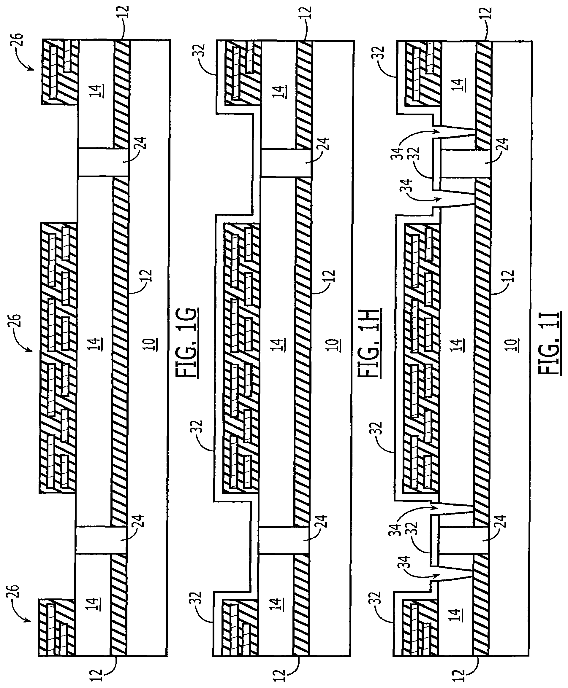
FIGS. 1F-1G illustrate forming a plurality of multi-layer electrical interconnect networks 26 on respective SOI substrates 20, after active devices (e.g., CMOS devices, not shown) have been formed therein. Each of these multi-layer electrical interconnect networks 26 may include multiple layers of metallization and vertical interconnects within a stacked composite of multiple interlayer insulating layers 28. As shown by FIG. 1G, an interlayer dielectric layer (ILD) etching step may be performed to expose the anchors 24, which may be ring-shaped or formed as parallel stripes that extend in a third dimension (see, e.g., FIG. 1K), and also expose adjacent portions of the semiconductor active layer 14. The exposed portions of the semiconductor active layer 14 illustrated by FIG. 1G can then be exposed to a plasma etchant to thereby roughen the exposed upper surfaces of the semiconductor active layer 14. Plasmas that operate to etch silicon may utilize fluorine-containing gases (e.g., sulfur hexafluoride, SF.sub.6). Alternatively, silicon may be removed from a surface of the active layer 14 by exposing the surface to a relatively inert gas containing argon ions, for example.
According to alternative embodiments of the invention (not shown), the intermediate structure illustrated by FIG. 1G may be achieved by providing an SOI substrate having active electronic devices (not shown) within the semiconductor active layer 14 and a plurality of multi-layer electrical interconnect networks on the active layer 14. The interlayer dielectric layers associated with the multi-layer electrically interconnect networks may then be selectively etched to expose the active layer 14 and then the active layer 14 and the sacrificial layer 12 may be selectively etched using a mask (not shown) to define a plurality of trenches having bottoms that expose the handling substrate 10. The trenches may then be filled with inorganic anchors prior to deposition of an inorganic capping layer.
Referring now to FIG. 1H, each of the plurality of multi-layer electrical interconnect networks 26 is encapsulated by depositing an inorganic capping layer 32 that contacts the roughened upper surfaces of the semiconductor active layer 14 to thereby form chemically impervious and etch resistant bonds (e.g., a hermetic seal) at the interface between the capping layer 32 and the roughened surfaces of the semiconductor active layer 14. The semiconductor capping layer 32 may be formed as an amorphous silicon layer or a metal layer. For example, an amorphous silicon capping layer may be deposited at a temperature of less than about 350.degree. C. using a plasma-enhanced deposition technique.
FIG. 1I illustrates the formation of through-substrate openings 34 by selectively patterning of the capping layer 32 to define openings therein followed by the deep etching of the semiconductor active layer 14 to thereby expose underlying portions of the sacrificial layer 12 and define relatively thin supporting tethers 36 (see, e.g., FIG. 1K). Referring now to FIG. 1J, the sacrificial layer 12 is selectively removed from between the semiconductor active layer 14 and the handling substrate 10 to thereby define a plurality of suspended integrated circuit chips 40 which are individually encapsulated by the patterned capping layer 32. During this removal step, which may include exposing the intermediate structure of FIG. 1I to hydrofluoric acid (HF), the sidewalls of the anchors 24 may be exposed and the capping layer 32 may operate to protect the electrical interconnect networks 26 from chemical etchants. FIG. 1K is a plan view of an integrated circuit substrate of FIG. 1J (with capping layer 32 removed), which shows thin supporting tethers 36 extending between adjacent portions of the semiconductor active layer 14. These supporting tethers 36 enable each of the integrated circuit chips 40 to remain attached to the anchors 24. The patterned capping layer 32 may also be removed or remain as a passivating/protective layer.
Referring now to FIG. 2, methods of forming a plurality of functional layers according to some embodiments of the invention include depositing a sacrificial layer on a substrate (step 1) and then patterning the sacrificial layer (step 2) into a plurality of sacrificial patterns. A functional layer is then deposited (step 3) onto the plurality of sacrificial patterns. The functional layer is then patterned (step 4) to define openings therein. The sacrificial patterns are then removed (step 5) from underneath respective functional patterns. The functional patterns are then transferred to another substrate (step 6) by printing, for example.
The methods of FIG. 2 are further illustrated by FIGS. 3A-3E, which are cross-sectional views of intermediate structures. These intermediate structures illustrate additional methods of forming substrates according to embodiments of the invention. FIG. 3A illustrates forming a sacrificial layer 52 on a handling substrate 50. The sacrificial layer 52 may be formed of an electrically conductive material such as molybdenum (Mo), aluminum (Al), copper (Cu), nickel (Ni), chromium (Cr), tungsten (W), titanium tungsten (TiW), titanium (Ti) or an electrically insulating material such as silicon dioxide, for example. The handling substrate 50 may be a semiconductor wafer, a glass substrate, or a ceramic board, for example. In some additional embodiments of the invention, a step may be performed to increase a roughness of an upper surface of the sacrificial layer 52 by exposing the upper surface to a chemical etchant for a sufficient duration to increase an average RMS roughness of the surface, prior to cleaning.
As illustrated by FIG. 3B, the sacrificial layer 52 is selectively etched using a mask (not shown) to define a plurality of spaced-apart sacrificial patterns 52' and expose portions of the underlying handling substrate 50, as illustrated. Referring now to FIG. 3C, a functional layer 54 is formed directly on upper surfaces of the plurality of spaced-apart sacrificial patterns 52' and directly on the exposed portions of the underlying handling substrate 50. The functional layer 54 may be formed as a semiconductor layer, such as a polysilicon layer, an amorphous silicon layer, a nanocrystalline silicon layer, or an indium gallium zinc oxide layer. The amorphous silicon layer may be formed using a plasma enhanced chemical vapor deposition (PECVD) technique. Alternatively, the polysilicon layer, amorphous silicon layer, nanocrystalline silicon layer or indium gallium zinc oxide layer may be formed using sputtering techniques.
Referring now to FIG. 3D, a patterned functional layer 54 is defined by selectively etching the functional layer 54 of FIG. 3C using a mask (not shown), to define a plurality of openings 56 therein that expose respective portions of the underlying sacrificial patterns 52'. As illustrated by FIG. 3E, a selective etching step is performed to remove the sacrificial patterns 52' from underneath the patterned functional layer 54 and thereby define a plurality of underlying gaps or recesses 55. This selective etching step may include exposing the sacrificial patterns 52' to a chemical etchant that passes through the openings in the functional layer 54 and removes the sacrificial patterns 52'.
As illustrated by FIG. 4A, the removal of the sacrificial patterns 52' may result in the formation of a plurality of suspended semiconductor device layers 54 that are attached by respective pairs of anchors 58 to a surrounding semiconductor layer. These anchors 58 are formed at diametrically opposite corners of the device layers 54, which are spaced apart from each other by respective openings 56. Referring now to FIG. 4B, the semiconductor device layers 54 may be printed at spaced-apart locations onto a second substrate 60 using a bonding technique. This printing step may also include fracturing the device layers 54 at the respective anchors 58 by removing the handling substrate 50 from the second substrate 60, so that the device layers 54 are provided at spaced locations on the second substrate 60.
Referring now to FIGS. 5 and 6A-6C, additional embodiments of the invention include depositing a sacrificial layer onto a first substrate 60 (step 1) and then patterning the sacrificial layer to define a plurality of openings therein (step 2) that extend between respective sacrificial patterns 62. A device layer 64 (e.g., amorphous semiconductor layer) is then deposited onto the patterned sacrificial layer and onto portions of the first substrate 60 exposed by the openings in the sacrificial layer (step 3). Portions of the device layer 64 are then treated by thermal and/or laser treatment. For example, in the event the device layer 64 is an amorphous silicon layer, then the portions of the device layer 64 extending opposite the plurality of spaced-apart sacrificial patterns 62 may be converted into respective semiconductor regions 65 having higher degrees of crystallinity therein relative to the surrounding amorphous silicon regions 64'.
The treated device layer 64 is then patterned (step 4) to define a plurality of openings 68 therein between amorphous silicon regions 64' and higher crystallinity regions 65'. These openings 68 expose respective ones of the plurality of spaced-apart sacrificial patterns 62. The sacrificial patterns 62 are then selectively etched through the openings (step 5) to thereby convert at least a first portion of the patterned device layer (e.g., amorphous semiconductor layer) into a plurality of suspended semiconductor device layers 65' that are anchored to a second portion of the patterned device layer 64'. As illustrated by FIGS. 4A-4B, a transfer printing step (step 6) may be performed to transfer the semiconductor device layers (as functional layers 54) to a second substrate 60.
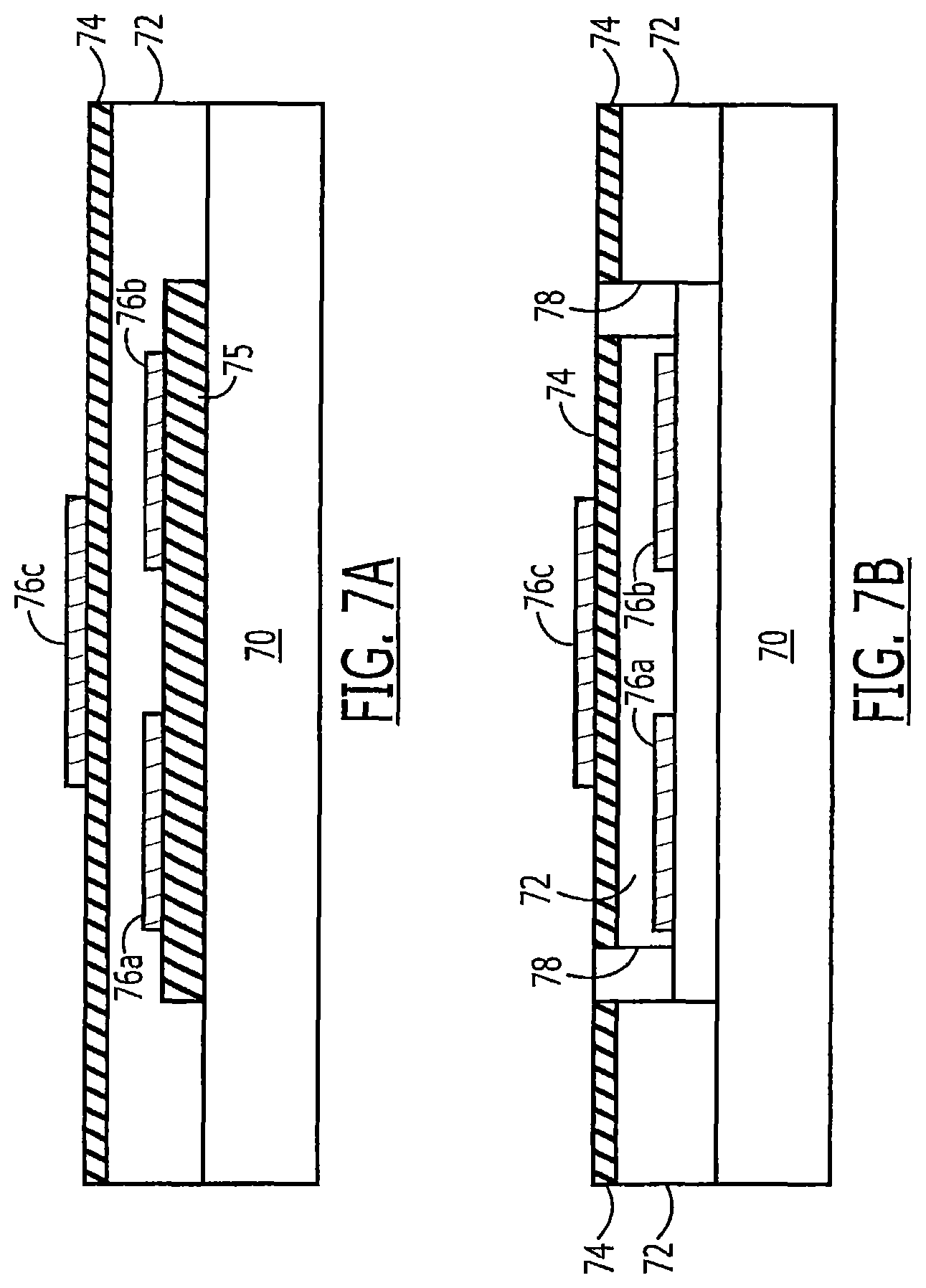
FIGS. 7A-7B illustrate methods of forming printable thin-film transistor (TFT) substrates according to additional embodiments of the invention. As illustrated by FIGS. 7A-7B, a sacrificial pattern 75 is formed on a first substrate 70. A source electrode 76a and a drain electrode 76b are formed on the sacrificial pattern 75, as illustrated. A semiconductor layer 72 (e.g., a-Si) is formed on the source and drain electrodes, the sacrificial pattern 75 and the substrate 70, as illustrated. Thereafter, an electrically insulating layer 74 is formed on the semiconductor layer 72 and a gate electrode 76c is formed on the electrically insulating layer 74. The source, drain and gate electrodes 76a-76c collectively define the three terminals of a thin-film transistor having an active channel region defined within the semiconductor layer 72. The insulating layer 74 and semiconductor layer 72 are then selectively etched to define openings 78 therein. An etching step (e.g., wet etching) is then performed to remove the sacrificial patter 75 from underneath the source and drain electrodes 76a-76b and the semiconductor layer 72, as illustrated. A printing step may then be performed to print the gate electrode 76c and insulating layer 74 directly onto a second substrate (not shown) prior to removal of the first substrate 70. This printing step results in the formation of a thin-film transistor (TFT) having exposed source and drain electrodes 76a-76b.
FIGS. 8A-8B illustrate methods of forming printable thin-film transistor (TFT) substrates according to additional embodiments of the invention. As illustrated by FIG. 8A-8B, a sacrificial pattern 85 is formed on a first substrate 80. A gate electrode 86c is formed on the sacrificial pattern 85, as illustrated. An electrically insulating layer 82 is then formed on the gate electrode 86c, the sacrificial pattern 85 and the substrate 80, as illustrated. Thereafter, a semiconductor layer 84 (e.g., a-Si) is formed on the electrically insulating layer 82. Source and drain electrodes 86a-86b are formed on the semiconductor layer 84. The source, drain and gate electrodes 86a-86c collectively define the three terminals of a thin-film transistor having an active channel region defined within the semiconductor layer 84. The semiconductor layer 84 and insulating layer 82 are then selectively etched to define openings 88 therein. An etching step (e.g., wet etching) is then performed to remove the sacrificial patter 85 from underneath the gate electrode 86c and the insulating layer 82, as illustrated. A printing step may then be performed to print the source and drain electrodes 86a-86b and semiconductor layer 84 directly onto a second substrate (not shown) prior to removal of the first substrate 80. This printing step results in the formation of a thin-film transistor (TFT) having an exposed gate electrode 86c.
FIGS. 9A-9B illustrate methods of forming printable thin-film transistor (TFT) substrates according to additional embodiments of the invention. As illustrated by FIGS. 9A-9B, a sacrificial pattern 95 is formed on a first substrate 90. A semiconductor layer 92 (e.g., a-Si) is formed on the sacrificial pattern 95 and the first substrate 90, as illustrated. Thereafter, an electrically insulating layer 94 having an embedded gate electrode 96a therein is formed on the semiconductor layer 92. Source and drain electrodes 96b-96c are then formed on the insulating layer 94. These source and drain electrodes use source and drain electrode plugs 96b' and 96c', which extend through the electrically insulating layer 94, to contact the semiconductor layer 92, as illustrated. The insulating layer 94 and semiconductor layer 92 are then selectively etched to define openings 98 therein. An etching step (e.g., wet etching) is then performed to remove the sacrificial patter 95 from underneath the semiconductor layer 92, as illustrated. A printing step may then be performed to print the source and drain electrodes 96b-96c and insulating layer 94 directly onto a second substrate (not shown) prior to removal of the first substrate 90. This printing step results in the formation of a thin-film transistor (TFT) having buried source and drain electrodes 96b-96c.
In the drawings and specification, there have been disclosed typical preferred embodiments of the invention and, although specific terms are employed, they are used in a generic and descriptive sense only and not for purposes of limitation, the scope of the invention being set forth in the following claims.
* * * * *
D00000
D00001
D00002
D00003
D00004
D00005
D00006
D00007
D00008
D00009
D00010
D00011
D00012

XML
uspto.report is an independent third-party trademark research tool that is not affiliated, endorsed, or sponsored by the United States Patent and Trademark Office (USPTO) or any other governmental organization. The information provided by uspto.report is based on publicly available data at the time of writing and is intended for informational purposes only.
While we strive to provide accurate and up-to-date information, we do not guarantee the accuracy, completeness, reliability, or suitability of the information displayed on this site. The use of this site is at your own risk. Any reliance you place on such information is therefore strictly at your own risk.
All official trademark data, including owner information, should be verified by visiting the official USPTO website at www.uspto.gov. This site is not intended to replace professional legal advice and should not be used as a substitute for consulting with a legal professional who is knowledgeable about trademark law.