Epitaxial growth of cubic and hexagonal InN films and their alloys with AlN and GaN
Nepal , et al. March 2, 2
U.S. patent number 10,937,649 [Application Number 14/571,826] was granted by the patent office on 2021-03-02 for epitaxial growth of cubic and hexagonal inn films and their alloys with aln and gan. This patent grant is currently assigned to The Government of the United States of America, as represented by the Secretary of the Navy. The grantee listed for this patent is Charles R. Eddy, Jr., Nadeemmullah A. Mahadik, Michael J. Mehl, Neeraj Nepal, Syed B. Qadri. Invention is credited to Charles R. Eddy, Jr., Nadeemmullah A. Mahadik, Michael J. Mehl, Neeraj Nepal, Syed B. Qadri.


| United States Patent | 10,937,649 |
| Nepal , et al. | March 2, 2021 |
Epitaxial growth of cubic and hexagonal InN films and their alloys with AlN and GaN
Abstract
Described herein is a method for growing InN, GaN, and AlN materials, the method comprising alternate growth of GaN and either InN or AlN to obtain a film of In.sub.xGa.sub.1-xN, Al.sub.xGa.sub.1-xN, Al.sub.xIn.sub.1-xN, or Al.sub.xIn.sub.yGa.sub.1-(x+y)N.
| Inventors: | Nepal; Neeraj (Woodbridge, VA), Eddy, Jr.; Charles R. (Columbia, MD), Mahadik; Nadeemmullah A. (Springfield, VA), Qadri; Syed B. (Fairfax Station, VA), Mehl; Michael J. (Davidsonville, MD) | ||||||||||
|---|---|---|---|---|---|---|---|---|---|---|---|
| Applicant: |
|
||||||||||
| Assignee: | The Government of the United States
of America, as represented by the Secretary of the Navy
(Washington, DC) |
||||||||||
| Family ID: | 1000005395975 | ||||||||||
| Appl. No.: | 14/571,826 | ||||||||||
| Filed: | December 16, 2014 |
Prior Publication Data
| Document Identifier | Publication Date | |
|---|---|---|
| US 20150140789 A1 | May 21, 2015 | |
Related U.S. Patent Documents
| Application Number | Filing Date | Patent Number | Issue Date | ||
|---|---|---|---|---|---|
| 13916724 | Jun 13, 2013 | 9773666 | |||
| 61661016 | Jun 18, 2012 | ||||
| Current U.S. Class: | 1/1 |
| Current CPC Class: | H01L 21/0242 (20130101); H01L 21/02381 (20130101); H01L 21/0262 (20130101); H01L 21/02458 (20130101); H01L 21/0254 (20130101); H01L 21/02433 (20130101); H01L 29/2003 (20130101); H01L 21/02661 (20130101); C30B 29/38 (20130101); C30B 29/403 (20130101); C30B 29/406 (20130101) |
| Current International Class: | H01L 21/02 (20060101); H01L 29/20 (20060101); C30B 29/38 (20060101); C30B 29/40 (20060101) |
References Cited [Referenced By]
U.S. Patent Documents
| 6136626 | October 2000 | Kidoguchi |
| 7521274 | April 2009 | Hersee et al. |
| 2002/0096683 | July 2002 | Ramdani |
| 2006/0163605 | July 2006 | Miyahara |
| 2007/0257264 | November 2007 | Hersee et al. |
| 2010/0065855 | March 2010 | Yokoyama |
| 2010/0163931 | July 2010 | Fujioka et al. |
| 2011/0147791 | June 2011 | Norman et al. |
| 2012/0052681 | March 2012 | Marsh |
| 2007-254175 | Oct 2007 | JP | |||
| 10-2009-0107403 | Oct 2009 | KR | |||
Other References
|
Atomic layer deposition of GaN at low temperatures, Cagla Ozgit, Inci Donmez, Mustafa Alevli, and Necmi Biyikli, J. Vac. Sci. Technol. A 30(1), Jan./Feb. 2012, pp. 01A124-1 to 01A124-4. cited by examiner . International Search Report and Written Opinion in PCT/US/2013/045569. cited by applicant . K. Mitamura et al: "Growth of InN films on spinel substrates by pulsed laser deposition," Phys. Stat. Sol. Rapid Research Letters, vol. I, No. 5, Oct. 2007 (Oct. 2007), pp. 211-213. cited by applicant . Stefano Orlando et al: "Structural, chemical, and electrical characterization of indium nitride produced by pulsed laser ablation," Phys. Status Solidi C: Current Topics in Solid State Physics, vol. 9, No. 3-4, Mar. 13, 2012 (Mar. 13, 2012), pp. 993-996. cited by applicant . C. Pinquier et al: "Raman scattering study of wurtzite and rocksalt InN under high pressure," Physical Review B, vol. 73, No. 11, Mar. 2006 (Mar. 2006), 115211. cited by applicant . Bhuiyan Ashraful Ghani et al: "Indium nitride (InN): A review on growth, characterization, and properties," Journal of Applied Physics, American Institute of Physics, US, vol. 94, No. 5, Sep. 2003 (Sep. 2003), pp. 2779-2808. cited by applicant . Zhang J et al: "Pulsed atomic layer epitaxy of quaternary AlinGaN layers," Applied Physics Letters, American Institute of Physics, vol. 79, No. 7, Aug. 13, 2001 (Aug. 13, 2001), pp. 925-927. cited by applicant . Keller S et al: "Flow Modulation Expitaxy of InN/GaN Heterostructures; Towards InN Based Hemts," Proceedings of International Workshop on Nitride Semiconductors, IPAP Conf. Series 1, pp. 233-236. cited by applicant . Extended European Search report for Application No. EP 13806353 completed on Jan. 14, 2016. cited by applicant . Original and English translation of Office Action dated Apr. 28, 2016 in Chinese patent application 201380032385.3. cited by applicant . S. Orlando et al.: "Structural, chemical, and electrical characterization of indium nitride" Phys. Status Solidi C 9, No. 3-4, 993-996 (2012). cited by applicant . Written Opinion in Singapore Patent Application No. 11201408484T. cited by applicant . J. Ibanez et al., Electronic structure of wurtzite and rocksalt InN investigated by optical absorption under hydrostatic pressure. Appl. Phys. Lett., May 18, 2010, vol. 96, 201903. cited by applicant . Cryst. Growth Des. 2013, 13, 1485-1490. cited by applicant. |
Primary Examiner: Qi; Hua
Attorney, Agent or Firm: US Naval Research Laboratory Roberts; Roy
Parent Case Text
CROSS-REFERENCE TO RELATED APPLICATIONS
This Application claims the benefit as a continuation-in-part of U.S. application Ser. No. 13/916,724 filed on Jun. 13, 2013 which in turn claims the benefit of U.S. Provisional Application 61/661,016 filed on Jun. 18, 2012.
Claims
What is claimed is:
1. A method for growing crystalline, epitaxial InN, GaN, and AlN materials, the method comprising alternate growth via plasma-assisted atomic layer epitaxy of GaN and either InN or AlN while using N.sub.2 plasma as a nitrogen precursor to obtain an epitaxial film of In.sub.xGa.sub.1-xN, Al.sub.xGa.sub.1-xN, Al.sub.xIn.sub.1-xN, or Al.sub.xIn.sub.yGa.sub.1-(x+y)N with an identical crystal structure throughout, wherein the method is effective to produce In.sub.xGa.sub.1-xN, Al.sub.xGa.sub.1-xN, Al.sub.xIn.sub.1-xN, or Al.sub.xIn.sub.yGa.sub.1-(x+y)N, materials such that x can be any number greater than 0 and less than 1 and, if present, y can also be any number from 0 to 1 as long as x+y totals between 0 and 1, inclusive; and wherein the method is performed entirely at a temperature of no greater than 500.degree. C.
2. The method of claim 1, using trimethylindium as an indium precursor.
3. The method of claim 1, using trimethylaluminum as an aluminum precursor.
4. The method of claim 1, using trimethylgallium as gallium precursor.
5. The method of claim 1, wherein InN is grown at a temperature of no greater than 300.degree. C.
6. A method for growing crystalline, epitaxial InN, GaN, and AlN materials, the method comprising alternate growth via plasma-assisted atomic layer epitaxy of GaN and either InN or AlN to obtain an epitaxial film of In.sub.xGa.sub.1-xN, Al.sub.xGa.sub.1-xN, or Al.sub.xIn.sub.1-xN with an identical crystal structure throughout, wherein the method is effective to produce In.sub.xGa.sub.1-xN, Al.sub.xGa.sub.1-xN, or Al.sub.xIn.sub.1-xN, materials such that x can be any number greater than 0 and less than 1; and wherein the method is performed entirely at a temperature of no greater than 500.degree. C.
7. The method of claim 6, using trimethylindium as an indium precursor.
8. The method of claim 6, using trimethylaluminum as an aluminum precursor.
9. The method of claim 6, using trimethylgallium as gallium precursor.
10. The method of claim 6, wherein InN is grown at a temperature of no greater than 300.degree. C.
Description
BACKGROUND
Among III-nitride semiconductors, indium nitride (InN) has the smallest direct band gap, largest electron saturation velocity and mobility, and smallest electron effective mass. It has long been an attractive semiconductor material for application in optical, electrical, and optoelectronic device technologies such as solar-cells and high electron mobility and high frequency devices. The most thermodynamically stable phase of the InN is a wurtzite structure (a hexagonal phase), however, the growth of zincblende (a cubic phase) InN on InAs/GaAs has been demonstrated at 450.degree. C. by plasma assisted molecular beam epitaxy (MBE). Cubic InN has a smaller band gap and superior electronic properties as its lattice is isotropic and possesses lower phonon scattering.
BRIEF SUMMARY
A method for growing InN, GaN and AlN materials includes alternate growth of these III-nitride binaries to obtain a film of In.sub.xGa.sub.1-xN or Al.sub.xGa.sub.1-xN or Al.sub.xIn.sub.1-xN or Al.sub.xIn.sub.yGa.sub.1-(x+y)N.
BRIEF DESCRIPTION OF THE DRAWINGS
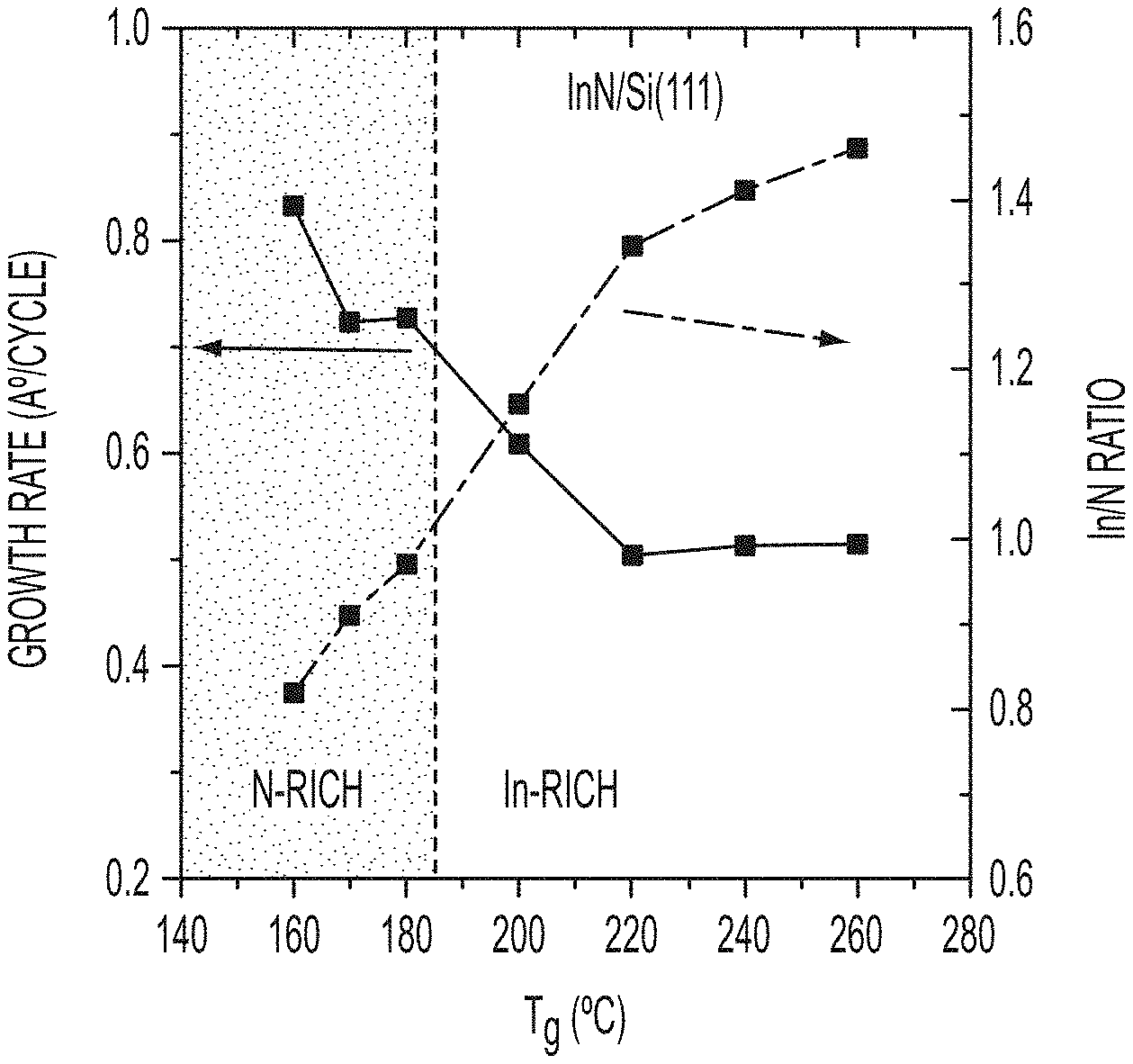
FIG. 1 shows variation of growth rate (GR) and In/N ratio with a trimethylindium (TMI) pulse of 0.06 seconds.
FIG. 2 depicts the x-ray diffraction (XRD) peaks from three of the samples--namely InN (60 nm) on GaN/Al.sub.2O.sub.3 template with T.sub.g=183.degree. C. (top) and on a-plane Al.sub.2O.sub.3 with T.sub.g=240.degree. C. (middle) and 183.degree. C. (bottom)).
FIG. 3 shows a schematic of the possible structure of a face centered cubic (fcc) InN phase and how it would align to an a-plane sapphire unit cell.
FIG. 4 depicts the variation of Al content in Al.sub.xIn.sub.1-xN with the AlN/InN cycles ratios in the whole range of x as determined by x-ray photoelectron spectroscopy. AlN and InN layers were grown as described herein where the aluminum precursor is trimethylaluminum, for example. First the InN was grown on GaN and then the AlN. Number of layers of InN and AlN were varied to get required concentration of Al content.
FIG. 5 depicts variation of Ga content in In.sub.xGa.sub.1-xN with GaN/InN cycles ratios in the range x as determined by x-ray photoelectron spectroscopy. InN and GaN layers were grown as described herein, but where gallium precursor is trimethylgallium, for example. First the InN was grown, followed by GaN. The number of layers of InN and GaN were varied to obtain the desired concentration of Ga content.
FIG. 6 depicts variation of Ga content in Al.sub.xGa.sub.1-xN with AlN/GaN cycles and ratios in the range of x as determined by x-ray photoelectron spectroscopy. AlN and GaN layers were grown as described herein, but where aluminum precursor is trimethlyaluminum, for example, and the gallium precursor is trimethylgallium, for example. First the AlN was grown, then the GaN. The number of layers of AlN and GaN were varied to obtain the desired Ga content.
DETAILED DESCRIPTION
Definitions
Before describing the present invention in detail, it is to be understood that the terminology used in the specification is for the purpose of describing particular embodiments, and is not necessarily intended to be limiting. Although many methods, structures and materials similar, modified, or equivalent to those described herein can be used in the practice of the present invention without undue experimentation, the preferred methods, structures and materials are described herein. In describing and claiming the present invention, the following terminology will be used in accordance with the definitions set out below.
As used herein, "low temperature" means temperatures lower than 400.degree. C., and if otherwise specified can refer to yet lower temperatures such as lower than 300.degree. C., as lower than 280.degree. C., lower than 260.degree. C., lower than 240.degree. C., lower than 220.degree. C., lower than 200.degree. C., lower than 180.degree. C., and so on.
Indium precursors include trimethylindium (TMI) and others known in the art.
Aluminum precursor includes trimethylaluminum (TMA) and others known in the art.
Gallium precursor includes trimethylgallium (TMG) and others known in the art.
As used in this specification and the appended claims, the singular forms "a", "an," and "the" do not preclude plural referents, unless the content clearly dictates otherwise.
As used herein, the term "and/or" includes any and all combinations of one or more of the associated listed items.
As used herein, the term "about" when used in conjunction with a stated numerical value or range denotes somewhat more or somewhat less than the stated value or range, to within a range of .+-.10% of that stated.
DESCRIPTION
InN layers were simultaneously grown using a Cambridge Nano Tech (CNT) Fiji 200 atomic layer deposition/epitaxy (ALE) system on a-plane sapphire, semi-insulating Si(111), and GaN/sapphire templates. Sapphire substrates were used to ensure unambiguous characterization of the electrical transport properties of the ALE InN layers on an insulator. Wafers were solvent cleaned and rinsed with deionized (DI) water before any further surface pretreatments. Si(111), GaN/sapphire, and sapphire surfaces were pretreated with HF, HF and 15% HCl, and solvents, respectively. The growth was carried out in an ultrahigh purity (UHP) argon (Ar) ambient. After ex situ surface pretreatment, substrates were treated with the 50 sccm N.sub.2 plasma at 300 watts before InN growth. About 150 to 1100 cycles of ALE deposition (see below) were used to synthesize InN films on different substrates simultaneously. The values of parameters given in this paragraph are examples, with other values possible.
FIG. 1 shows variation of growth rate (GR) and In/N ratio with a trimethylindium (TMI) pulse of 0.06 seconds. The GR was decreased from 0.83 to 0.73 .ANG. with increasing temperature from 160 to 183.degree. C. It remains constant for a small temperature window and decreases again to 0.51 .ANG. at 220.degree. C. For T.sub.g between 220-260.degree. C., the GR remains constant. The temperature range between 220-260.degree. C. is the second atomic layer epitaxy (ALE) window. In the first low temperature ALE window the InN growth is N-rich (In/N<1) and it is In-rich (In/N>1) for the high temperature ALE window. An In/N ratio of 2.8.+-.0.7 has been measured on MBE grown InN (see Piper et al., J. Vac. Sci. Technol. A 23, 617 (2005)). Thus, the ALE InN has better stoichiometry.
FIG. 2 depicts the XRD peaks from three of the samples--namely InN (60 nm) on GaN/Al.sub.2O.sub.3 template with T.sub.g=183.degree. C. (top) and on a- plane Al.sub.2O.sub.3 with T.sub.g=240.degree. C. (middle) and 183.degree. C. (bottom)). The top plot indicates the material has a hexagonal phase. In the bottom plot, there are a set of peaks that could be indexed to either a face centered cubic (FCC) structure with the (200) and (400) indices, or a CsCl structure with (110) and (220) indices. Also measured were the 24 hr long Laue diffraction (LD) patterns on this sample in transmission as well as grazing incidence reflection mode. In both modes Laue spots were observed, indicating that this sample has an epitaxial nature and not a powder/polycrystalline nature. This is also confirmed with the second order peak in the bottom plot which has resolved in the K.alpha..sub.1 and K.alpha..sub.2 components (inset). This peak is obtained via a 15 summation scan to enhance the signal. The FWHM values are 494 and 371 arc-secs for the first and second order peaks, respectively. The first order peak is a convolution of the two K.alpha. components. In order to confirm the structure, the third order peak was examined, which was not measurable since it occurs at much higher angles and the sample is only 60 nm thick. Also, the d-spacings of the first two peaks do not match to any InN phases in the ICDD database. The results suggest that the InN on a sapphire at 183.degree. C. has a highly oriented epitaxial structure. Further analysis of the data reveals that the d spacings (6.68 A) of the first peak do not match to any of the known InN phases in the reported international center for diffraction data (ICDD) database and instead corresponds to a face centered cubic (FCC) structure which has not been reported before. The XRD data was corroborated by electron microscopy as described in Cryst. Growth Des. 2013, 13, 1485-1490, incorporated herein by reference.
FIG. 3 shows a schematic of the alignment of a face centered cubic (fcc) InN phase unit cell with an a-plane sapphire substrate unit cell. From the measured lattice parameter of the InN film assuming the FCC structure, we see that it has only a 2.8% mismatch with the in-plane c-direction and a 18.9% mismatch with the in-plane m-direction of sapphire. This is further indication that this is the most likely phase of the grown InN film on a-plane sapphire.
There has been a previous report (see ref. 21) of cubic InN growth at 450.degree. C. by plasma-assisted molecular beam epitaxy (MBE) on InAs/GaAs, but the InN is demonstrated to have a ZnS (zincblende) phase rather than a NaCl-type phase as obtained herein.
Table 1 summarizes different parameters and their values to synthesize various materials. Each ALE cycle consisted of first a 60 ms trimethylindium (TMI) pulse (which was empirically found as self-limited ALE growth mode, with longer pulses not providing significantly greater growth), which were added to a constant 30 and 100 sccm flow of UHP argon carrier gas. After each TMI pulse, the main pumping valve was closed for 5 sec so that the surface would saturate with In atoms. A 20 second long 300 watt N.sub.2 plasma exposure was used to provide nitrogen precursor to the indium saturated surface. To remove unreacted precursors, the deposition chamber was purged with UHP argon for 10 s after each pulse. The reactor chuck was heated resistively, and the temperature was calibrated using thermocouple and by pyrometer by CNT. The values of parameters given are examples. Other values are possible.
TABLE-US-00001 TABLE I growth parameters for ALE of InN Parameters TMI Pulse Purge 300 W N.sub.2 Plasma Plasma pulse Purge Number of cycles Studied range 0.015-0.1 sec 5-15 sec 50-150 sccm 10-30 sec 5-15 sec 150-1100 Established value 0.06 sec 10 sec 100 sccm 20 sec 10 sec --
Table II summarizes different parameters and their values to synthesize various materials that contain aluminum. Each ALE cycle consisted of first a 60 ms trimethylaluminum (TMA) pulse (which was empirically found as self-limited ALE growth mode, with longer pulses not providing significantly greater growth), which were added to a constant 30 and 100 sccm flow of UHP argon carrier gas. After each TMA pulse, a 20 second long 300 watt N2/H2 plasma exposure was used to provide nitrogen precursor to the aluminum saturated surface. To remove unreacted precursors, the deposition chamber was purged with UHP argon for 10 s after each pulse. The reactor chuck was heated resistively, and the temperature was calibrated using thermocouple and by pyrometer by CNT. The values of parameters given are examples. Other values are possible.
For the ALE growth of AlInN, InN and AlN layers were grown layer by layer in the fashion of a digital alloy. To grow Al.sub.0.90In.sub.0.10N, AlN and InN were grown alternatively. For an AlN cycle for every two cycles of InN results in Al.sub.0.79In.sub.0.21N. For an AlN cycle for every three cycles of InN results Al.sub.0.68In.sub.0.32N. Thus by changing the combination of number layers of InN and AlN, Al.sub.xIn.sub.1-xN films can be obtained in for the full range of x (0 to 1) via atomic layer epitaxy. In this manner, AlInN ternary alloys are realized over the entire desired stoichiometry range--this is believed to be the first time this was accomplished. The values of parameters given are examples. Other values are possible.
TABLE-US-00002 TABLE II growth parameters for ALE of A1N Parameters TMA Pulse Purge 300 W N.sub.2/H.sub.2 Plasma Plasma pulse Purge Studied range 0.03-0.1 sec 5-40 sec N.sub.2 only - N.sub.2:H.sub.2 = 1:3 10-30 sec 5-40 sec Established value 0.06 sec 10 sec 42/8 sccm 20 sec 10 sec
Table III summarizes different parameters and their values to synthesize various materials that contain gallium. Each ALE cycle consisted of first a 15 ms trimethylgallium (TMG) pulse (which was empirically found as self-limited ALE growth mode, with longer pulses not providing significantly greater growth), which were added to a constant 30 and 100 sccm flow of UHP argon carrier gas. After each TMG pulse, a 20 second long 300 watt N.sub.2 plasma exposure was used to provide nitrogen precursor to the gallium saturated surface. To remove unreacted precursors, the deposition chamber was purged with UHP argon for 10 s after each pulse. The reactor chuck was heated resistively, and the temperature was calibrated using thermocouple and by pyrometer by CNT. The values of parameters given are examples. Other values are possible
For the ALE growth of InGaN, InN and GaN layers were grown layer by layer in the fashion of a digital alloy. To grow In.sub.0.60Ga.sub.0.40N, GaN and InN were grown alternatively. Conducting two GaN cycles for every InN cycle results in In.sub.0.45Ga.sub.0.55N. Conducting three GaN cycles for every InN cycle results in In.sub.0.37Ga.sub.0.63N. Thus, by changing the combination of number layers of InN and GaN, In.sub.xGa.sub.1-xN films can be obtained in for the full range of x (0 to 1, inclusive) via atomic layer epitaxy. In this manner, InGaN ternary alloys are realized over the entire desired stoichiometric range--this is believed to be the first time this was accomplished. The values of parameters given are examples. Other values are possible.
TABLE-US-00003 TABLE III Growth Parameters for ALE of GaN Parameters TMG Pulse Purge 300 W N.sub.2/H.sub.2 Plasma Plasma Pulse Purge Studied Range 0.005-0.1 sec 1-40 sec N.sub.2 only (5-200 sccm); 1-30 sec 1-30 sec N.sub.2:H.sub.2 = 1:1 to 7:1 Established Value 0.015 sec 10 sec N.sub.2 only (75 sccm) 20 sec 10 sec
For the ALE growth of AlGaN, AlN and GaN layers were grown layer by layer in the fashion of a digital alloy. To grow A.sub.0.85Ga.sub.0.15N, AlN and GaN were grown alternatively. For two GaN cycles for every AlN cycle results in Al.sub.0.75Ga.sub.0.25N. For three GaN cycles for every AlN cycle results in Al.sub.0.60Ga.sub.0.40N. Thus by changing the combination of number layers of AlN and GaN, Al.sub.xGa.sub.1-xN films can be obtained in for the full range of x (0 to 1, inclusive) via atomic layer epitaxy. In this manner, AlGaN ternary alloys are realized over the entire desired stoichiometric range--this is believed to be the first time this was accomplished at temperatures below 700.degree. C. The values of parameters given are examples. Other values are possible.
InN was grown at temperatures as low as room temperature (about 25.degree. C.) and as high as 300.degree. C., for example at 183.degree. C. GaN was grown at temperatures as low as room temperature (about 25.degree. C.) and as high as 500.degree. C., for example at 400.degree. C. AlN was grown at temperatures as low as room temperature (about 25.degree. C.) and as high as 650.degree. C., for example at 500.degree. C. The ternary materials that mix these binaries can be grown at temperatures suitable for a combination of those binaries. AlGaN ternaries were grown at low as room temperature (about 25.degree. C.) and as high as 500.degree. C., for example at 400.degree. C. AlInN ternaries were grown at low as room temperature (about 25.degree. C.) and as high as 500.degree. C., for example at 260.degree. C. InGaN ternaries were grown at low as room temperature (about 25.degree. C.) and as high as 400.degree. C., for example at 260.degree. C.
Substrates of silicon, gallium nitride, and sapphire have been employed for the above methods. It is believed that any standard substrate used in the art would be suitable.
Quaternary alloys of the form Al.sub.xIn.sub.yGa.sub.1-(x+y)N are also believed to be obtainable using the above techniques. It is expected that the full range of x and y would be achievable.
The techniques described herein are expected to provide a crystalline material having low oxygen impurity by ex situ and in situ surface treatment. Moreover, in situ surface treatment with the atomic hydrogen, nitrogen, mixture of hydrogen and nitrogen, and/or ammonia plasma is possible. It is possible to vary purge time with the pumping speed in order to control carbon impurities.
Concluding Remarks
All documents mentioned herein are hereby incorporated by reference for the purpose of disclosing and describing the particular materials and methodologies for which the document was cited.
Although the present invention has been described in connection with preferred embodiments thereof, it will be appreciated by those skilled in the art that additions, deletions, modifications, and substitutions not specifically described may be made without departing from the spirit and scope of the invention. Terminology used herein should not be construed as being "means-plus-function" language unless the term "means" is expressly used in association therewith.
REFERENCES
Each of the following is incorporated herein by reference, particularly for the teaching for which it was cited.
1. Y. Nanishi, Y. Saito, and T. Yamaguchi, Jpn. J. Appl. Phys. 42, 2549 (2003) and the references therein.
2. A. G. Bhuiyan, A. Hashimoto, and A. Yamamoto, J. Appl. Phys. 94, 2779 (2003).
3. N. Dietz, M. Alevli, V. Woods, M. Strassburg, H. Kang, and I. T. Ferguson, Phys. Status Solidi B 242, 2985 (2005).
4. R. P. Bhatta, B. D. Thoms, A. Weerasekera, A. G. U. Perera, M. Alevli, and N. Dietz, J. Vac. Sci. Technol. 25, 967 (2007).
5. Shou-Yi Kuo, Fang-I Lai, Wei-Chun Chen, Woei-Tyng Lin, Chien-Nan Hsiao, Hsin-I Lin, and Han-Chang Pan, Diamond & Related Materials 20, 1188 (2011).
6. M. A. Hafez and H. E. Elsayed-Ali, J. Vac. Sci. Technol. A 27, 696 (2009).
7. K. S. Boutros, F. G. McIntosh, J. C. Roberts, S. M. Bedair, E. L. Piner, and N. A. El-Masry. Appl. Phys. Lett. 67, 1856 (1995).
8. C. Ozgit, I. Donmez, M. Alevli, and N. Biyikli, J. Vac. Sci. Technol. A 30, 01A124 (2012).
9. N. H. Karam, T. Parodos, P. Colter, D. McNulty, W. Rowland, J. Schetzina, N. El-Masry, and S. M. Bedair, Appl. Phys. Lett. 67, 94 (1995).
10. K. Kim, N. Kwak, and S. Lee, Electron. Mater. Lett. 5, 83 (2009).
11. M. Alevli, C. Ozgit, I. Donmez, and N. Biyikli, Phys. Status Solidi A 209, 266 (2012).
12. O. Ambacher, M. S. Brandt, R. Dimitrov, T. Metzger, M. Stutzmann, R. A. Fischer, A. Miehr, A. Bergmaier, and G. Dollinger, J. Vac. Sci. Technol. B 14, 3532 (1996). InN dissociation temp 630
13. M. Y. Duan, L He, M. Xu, M. Y. Xu, Shuyan Xu, and K. Ostrikov, Phys. Rev. B 81, 033102 (2010).
14. A. Yamamoto, T. Shin-ya, T. Sugiura, A. Hashimoto, J. Cryst. Growth, 189/190, 461 (1998).
15. J. G. Lozano, F. M. Morales, R. Garcia, D. Gonzalez, V. Lebedev, Ch. Y. Wang, V. Cimalla, and O Ambacher, Appl. Phys. Lett. 90, 091901 (2007).
16. A. Janotti and C, G. Van de Walle, Appl. Phys. Lett. 92, 032104 (2008).
17. L. F. J. Piper, T. D. Veal, M. Walker, I. Mahboob, C. F. McConville, H. Lu, and W. J. Schaff, J. Vac. Sci. Technol. A 23, 617 (2005)
18. C. G. Van de Walle, J. L. Lyons, and A. Janotti, Solidi A 207, 1024 (2010).
19. T. Matsuoka, H. Okamoto, M. Nakao, H. Harima, and E. Kurimoto, Appl. Phys. Lett. 81, 1246 (2002).
20. M. C. Lee, H. C. Lin, Y. C. Pan, C. K. Shu, J. Ou, W. H. Chen, and W. K. Chen, Appl. Phys. Lett. 73, 2606 (1998).
21. A. P. Lima, A. Tabata, J. R. Leite, S. Kaiser, D. Schikora, B. Schottker, T. Frey, D. J. As, and K. Lischka, J. Cryst. Growth, 201/202, 396 (1999).
* * * * *
D00000
D00001
D00002
D00003
D00004
D00005
D00006
XML
uspto.report is an independent third-party trademark research tool that is not affiliated, endorsed, or sponsored by the United States Patent and Trademark Office (USPTO) or any other governmental organization. The information provided by uspto.report is based on publicly available data at the time of writing and is intended for informational purposes only.
While we strive to provide accurate and up-to-date information, we do not guarantee the accuracy, completeness, reliability, or suitability of the information displayed on this site. The use of this site is at your own risk. Any reliance you place on such information is therefore strictly at your own risk.
All official trademark data, including owner information, should be verified by visiting the official USPTO website at www.uspto.gov. This site is not intended to replace professional legal advice and should not be used as a substitute for consulting with a legal professional who is knowledgeable about trademark law.