Method for manufacturing resin-sealed power semiconductor device
Ichikawa , et al. February 23, 2
U.S. patent number 10,930,523 [Application Number 16/078,642] was granted by the patent office on 2021-02-23 for method for manufacturing resin-sealed power semiconductor device. This patent grant is currently assigned to Mitsubishi Electric Corporation. The grantee listed for this patent is Mitsubishi Electric Corporation. Invention is credited to Kazuo Funahashi, Keitaro Ichikawa, Ken Sakamoto.


| United States Patent | 10,930,523 |
| Ichikawa , et al. | February 23, 2021 |
Method for manufacturing resin-sealed power semiconductor device
Abstract
It is an object of the present invention to provide a method for manufacturing a resin-sealed power semiconductor device that facilitates the separation of a suspension lead from a mold resin and a lead frame. A method for manufacturing a resin-sealed power semiconductor device according to the present invention includes the following steps: (a) sealing a semiconductor element and a lead frame, to prepare a sealed body in which a terminal lead and a suspension lead that are included in the lead frame project outward from a side of the mold resin; (b) punching a portion of the suspension lead, the portion projecting from the mold resin, with a first punch in a first direction, to separate the suspension lead from the mold resin; and (c) punching the projecting portion of the suspension lead with a second punch in a second direction.
| Inventors: | Ichikawa; Keitaro (Tokyo, JP), Sakamoto; Ken (Tokyo, JP), Funahashi; Kazuo (Tokyo, JP) | ||||||||||
|---|---|---|---|---|---|---|---|---|---|---|---|
| Applicant: |
|
||||||||||
| Assignee: | Mitsubishi Electric Corporation
(Tokyo, JP) |
||||||||||
| Family ID: | 59963691 | ||||||||||
| Appl. No.: | 16/078,642 | ||||||||||
| Filed: | March 29, 2016 | ||||||||||
| PCT Filed: | March 29, 2016 | ||||||||||
| PCT No.: | PCT/JP2016/059998 | ||||||||||
| 371(c)(1),(2),(4) Date: | August 22, 2018 | ||||||||||
| PCT Pub. No.: | WO2017/168537 | ||||||||||
| PCT Pub. Date: | October 05, 2017 |
Prior Publication Data
| Document Identifier | Publication Date | |
|---|---|---|
| US 20190051539 A1 | Feb 14, 2019 | |
| Current U.S. Class: | 1/1 |
| Current CPC Class: | H01L 23/49517 (20130101); H01L 21/4842 (20130101); H01L 23/3121 (20130101); H01L 23/48 (20130101); H01L 23/42 (20130101); H01L 23/49541 (20130101); H01L 21/565 (20130101); H01L 23/50 (20130101) |
| Current International Class: | H01L 21/48 (20060101); H01L 23/495 (20060101); H01L 23/48 (20060101); H01L 23/50 (20060101); H01L 23/42 (20060101); H01L 21/56 (20060101); H01L 23/31 (20060101) |
References Cited [Referenced By]
U.S. Patent Documents
| 9202765 | December 2015 | Wang |
| 2002/0020929 | February 2002 | Kasuga |
| 2002/0024127 | February 2002 | Sakuraba |
| 2005/0116327 | June 2005 | Danno |
| 2007/0232027 | October 2007 | Kumamoto |
| 2008/0061413 | March 2008 | Otremba |
| 2011/0198739 | August 2011 | Amanai |
| 2011/0300670 | December 2011 | Tanaka |
| 2012/0196405 | August 2012 | Sakamoto |
| 2013/0341779 | December 2013 | Sakamoto |
| 2014/0225239 | August 2014 | Kimura |
| 2014/0353814 | December 2014 | Sakamoto |
| 2016/0190115 | June 2016 | Shigematsu |
| 2018/0040487 | February 2018 | Takahashi |
| 2019/0291160 | September 2019 | Fortmeier |
| H06-005758 | Jan 1994 | JP | |||
| H11-319977 | Nov 1999 | JP | |||
| 2013-239625 | Nov 2013 | JP | |||
Other References
|
International Search Report issued in PCT/JP2016/059998; dated Jun. 7, 2016. cited by applicant. |
Primary Examiner: Menz; Laura M
Assistant Examiner: Rahman; Khatib A
Attorney, Agent or Firm: Studebaker & Brackett PC
Claims
The invention claimed is:
1. A method for manufacturing a resin-sealed power semiconductor device, comprising the steps of: (a) sealing a semiconductor element and a lead frame electrically connected to the semiconductor element with a mold resin, to prepare a sealed body in which a terminal lead and a suspension lead that are directly connected to the lead frame project outward from a side of the mold resin, wherein the terminal lead, the suspension lead and the lead frame are different elements; (b) punching a portion of the suspension lead, the portion projecting from the mold resin, with a first punch in a first direction oriented from a one-main-surface side of the mold resin to an other-main-surface side opposite to the one-main-surface side, to separate the projecting portion of the suspension lead from the mold resin; and (c) punching the projecting portion of the suspension lead with a second punch in a second direction oriented from the other-main-surface side of the mold resin to the one-main-surface side, to separate the suspension lead from the lead frame.
2. The method for manufacturing a resin-sealed power semiconductor device according to claim 1, wherein the one-main-surface side is a heat dissipation surface of the mold resin.
3. The method for manufacturing a resin-sealed power semiconductor device according to claim 2, wherein the step (c) is performed after the step (b).
4. The method for manufacturing a resin-sealed power semiconductor device according to claim 1, wherein in the step (b), a tip of the suspension lead located within the mold resin, the tip being located on a separation side, is separated so as not to project from the mold resin.
5. The method for manufacturing a resin-sealed power semiconductor device according to claim 2, wherein a distance between the one-main-surface side of the mold resin and a surface of the suspension lead on the one-main-surface side is 1.6 mm or greater.
6. A method for manufacturing a resin-sealed power semiconductor device, comprising the steps of: (a) sealing a semiconductor element and a lead frame electrically connected to the semiconductor element with a mold resin, to prepare a sealed body in which a terminal lead and a suspension lead that are directly connected to the lead frame project outward from a side of the mold resin; (b) punching a portion of the suspension lead, the portion projecting from the mold resin, with a first punch in a first direction oriented from a one-main-surface side of the mold resin to an other-main-surface side opposite to the one-main-surface side, to separate the projecting portion of the suspension lead from the mold resin; and (c) punching the projecting portion of the suspension lead with a second punch in a second direction oriented from the other-main-surface side of the mold resin to the one-main-surface side, to separate the suspension lead from the lead frame, such that the terminal lead is coupled to the lead frame when the suspension lead is separated from the lead frame.
7. A method for manufacturing a resin-sealed power semiconductor device, comprising the steps of: (a) sealing a semiconductor element and a lead frame electrically connected to the semiconductor element with a mold resin, to prepare a sealed body in which a terminal lead and a suspension lead that are directly connected to the lead frame project outward from a side of the mold resin; (b) punching a portion of the suspension lead, the portion projecting from the mold resin, with a first punch in a first direction oriented from a one-main-surface side of the mold resin to an other-main-surface side opposite to the one-main-surface side, to separate the projecting portion of the suspension lead from the mold resin; and (c) punching the projecting portion of the suspension lead with a second punch in a second direction oriented from the other-main-surface side of the mold resin to the one-main-surface side, to separate the suspension lead from the lead frame, such that the terminal lead is electrically connected to the semiconductor element, and the suspension lead is not electrically connected to the semiconductor element.
Description
TECHNICAL FIELD
The present invention relates to a method for manufacturing a resin-sealed power semiconductor device.
BACKGROUND ART
Resin-sealed power semiconductor devices each include a conductor stacked on an insulating substrate dissipating heat, a power semiconductor elements joined to the conductor, and a wire electrically conducting the power semiconductor element and a terminal lead together. The insulating substrate, the conductor, the power semiconductor element, and the wire are sealed with a mold resin. The terminal lead extends outward from a side of the mold resin. The terminal lead has one end connected to the wire and positioned inside the resin, and the other end positioned outside the resin. It is noted that such a resin seal type is also referred to as a transfer mold type.
The power semiconductor element is electrically connected to a lead frame, and is connected to the terminal lead through the wire in the production of such a resin-sealed power semiconductor device. The lead frame includes the terminal lead and a suspension lead that is not electrically connected to the semiconductor element. The suspension lead is used to enhance wire-bonding performance in a wire-bonding step of connecting the wire to the power semiconductor element and the terminal lead, or is used to fix a semiconductor device, such as a power semiconductor device in a resin-sealing step. After the resin-sealing step, the suspension lead projects outward from a side of the mold resin; that is, the mold resin is connected to the lead frame through the suspension lead. In the suspension lead, a portion projecting from the mold resin is separated from the mold resin and the lead frame with a tool, such as a punch.
A technique of suspension-lead separation from the mold resin and the lead frame has been conventionally disclosed (c.f., Patent Document 1).
PRIOR ART DOCUMENT
Patent Document
Patent Document 1: Japanese Patent Application Laid-Open No. 2013-239625
SUMMARY
Problem to be Solved by the Invention
Patent Document 1 describes, in a comparative example, that the suspension lead is separated from the mold resin and the lead frame through a one-time punching step with the mold resin and the lead frame connected to the suspension lead (c.f., Patent Document 1; FIGS. 7 to 9). This separation unfortunately produces a burr in a separated portion between the lead frame and the suspension lead. Meanwhile, Patent Document 1 requires slits in the lead frame in order to solve this problem in the comparative example.
The present invention has been made to solve the above problem. It is an object of the present invention to provide a method for manufacturing a resin-sealed power semiconductor device that facilitates the separation of a suspension lead from a mold resin and a lead frame.
Means to Solve the Problem
To solve the above problem, the present invention provides a method for manufacturing a resin-sealed power semiconductor device, including the following steps: (a) sealing a semiconductor element and a lead frame electrically connected to the semiconductor element with a mold resin, to prepare a sealed body in which a terminal lead and a suspension lead that are included in the lead frame project outward from a side of the mold resin; (b) punching a portion of the suspension lead, the portion projecting from the mold resin, with a first punch in a first direction oriented from a one-main-surface side of the mold resin to an other-main-surface side opposite the one main surface, to separate the suspension lead from the mold resin; and (c) punching the projecting portion of the suspension lead with a second punch in a second direction oriented from the other-main-surface side of the mold resin to the one-main-surface side, to separate the suspension lead from the lead frame.
Effects of the Invention
According to the present invention, the method for manufacturing a resin-sealed power semiconductor device includes the following steps: (a) sealing a semiconductor element and a lead frame electrically connected to the semiconductor element with a mold resin, to prepare a sealed body in which a terminal lead and a suspension lead that are included in the lead frame project outward from a side of the mold resin; (b) punching a portion of the suspension lead, the portion projecting from the mold resin, with a first punch in a first direction oriented from a one-main-surface side of the mold resin to an other-main-surface side opposite the one main surface, to separate the suspension lead from the mold resin; and (c) punching the projecting portion of the suspension lead with a second punch in a second direction oriented from the other-main-surface side of the mold resin to the one-main-surface side, to separate the suspension lead from the lead frame. The method facilitates the separation of the suspension lead from the mold resin and the lead frame.
These and other objects, features, aspects and advantages of the present invention will become more apparent from the following detailed description of the present invention when taken in conjunction with the accompanying drawings.
BRIEF DESCRIPTION OF DRAWINGS
FIG. 1 is a plan view of one example of a resin-sealed power semiconductor device according to an embodiment of the present invention.
FIG. 2 is a plan view of one example of a step for manufacturing the resin-sealed power semiconductor device according to the embodiment of the present invention.
FIG. 3 is a cross-sectional view of one example of a step for manufacturing the resin-sealed power semiconductor device according to the embodiment of the present invention.
FIG. 4 is a plan view of one example of a step for manufacturing the resin-sealed power semiconductor device according to the embodiment of the present invention.
FIG. 5 is a plan view of one example of a step for manufacturing the resin-sealed power semiconductor device according to the embodiment of the present invention,
FIG. 6 is a cross-sectional view of one example of a suspension lead in the resin-sealed power semiconductor device according to the embodiment of the present invention.
FIG. 7 is a cross-sectional view of one example of the suspension lead in the resin-sealed power semiconductor device according to the embodiment of the present invention.
FIG. 8 is a cross-sectional view of one example of the suspension lead in the resin-sealed power semiconductor device according to the embodiment of the present invention.
FIG. 9 is a plan view of one example of a conventional resin-sealed power semiconductor device.
DESCRIPTION OF EMBODIMENT(S)
The following describes an embodiment of the present invention with reference to the drawings.
Embodiment
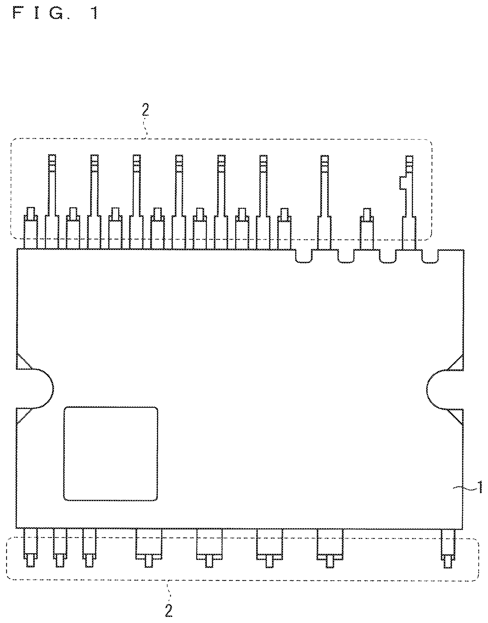
FIG. 1 is a plan view of one example of a resin-sealed power semiconductor device according to the embodiment of the present invention.
The resin-sealed power semiconductor device includes a semiconductor element (not shown) that is electrically connected to a copper lead frame and is a PW chip, a semiconductor element (not shown) that is electrically connected to the copper lead frame and is an IC chip, and a plurality of wires (not shown) electrically connecting terminal leads 2 of the lead frame and each semiconductor element together. These components are sealed with a mold resin 1. The terminal leads 2 project outward from the sides of the mold resin 1. The plurality of wires include thick wires and thin wires. It is noted that the lead frame corresponds to a lead frame 4 in FIG. 2, which will be described later on.
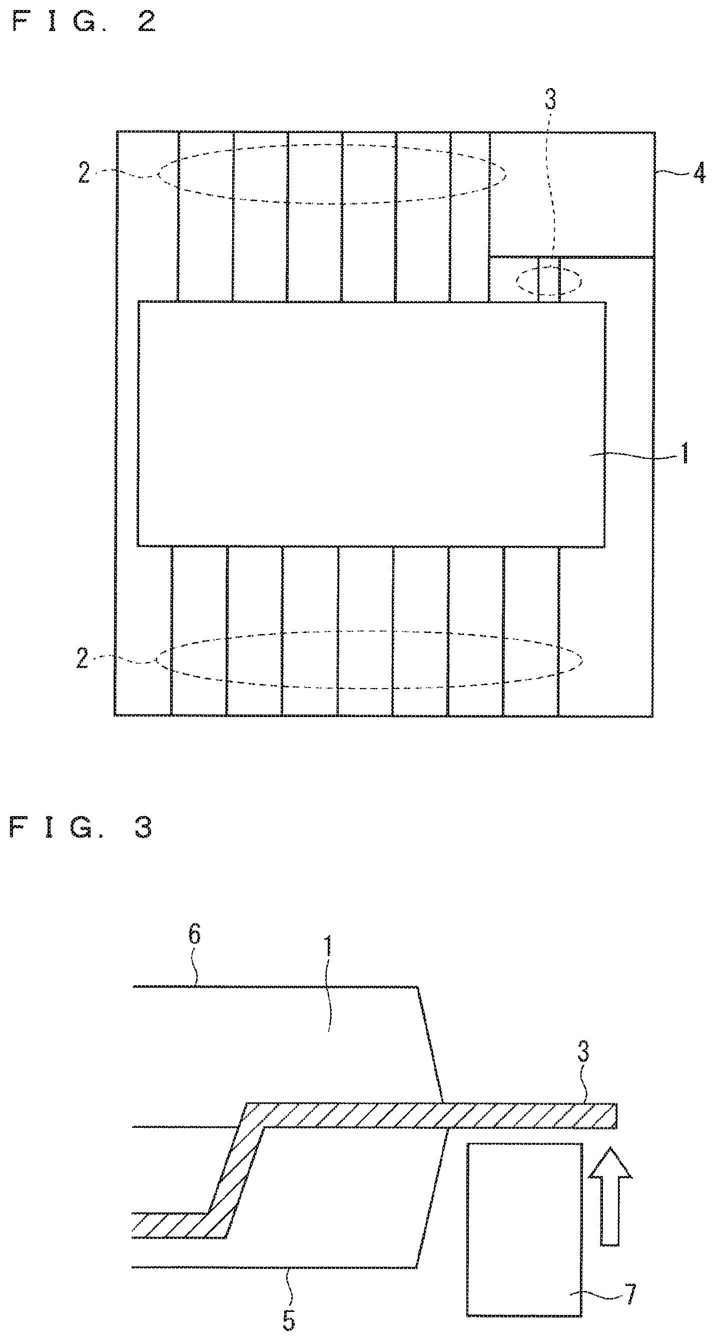
FIGS. 2 to 5 illustrate examples of process steps for manufacturing the resin-sealed power semiconductor device according to the embodiment. It is noted that the steps in FIGS. 2 to 5 are preformed through a well-known tie-bar cut process (T/C process) or a well-known lead cut process (L/C process).
As illustrated in FIG. 2, the semiconductor elements and the lead frame 4, which is electrically connected to the semiconductor elements, are sealed with the mold resin 1, to prepare a sealed body in which the terminal lead 2 and a suspension lead 3 that are included in the lead frame 4 project outward from the side of the mold resin 1.
As illustrated in FIG. 3, a portion of the suspension lead 3, the portion projecting from the mold resin 1, next undergoes punching with a punch 7 that is a first punch in a first direction oriented from a heat-dissipation-surface-5 side that is one main surface of the mold resin 1 to an upper-surface-6 side that is the other main surface opposite the heat dissipation surface, to be separated from the mold resin 1. As illustrated in FIG. 4, the suspension lead 3 is connected to the lead frame 4 while separated from the mold resin 1 at this time. It is noted that the first direction corresponds to a direction indicated by an arrow in FIG. 3.
The suspension lead 3, which is connected to the lead frame 4, next undergoes punching with a second punch (not shown) in a second direction oriented from the upper-surface-6 side of the mold resin 1 to the heat-dissipation-surface-5 side, to be separated from the lead frame 4. FIG. 5 illustrates the suspension lead 3 as separated from the lead frame 4.
Then, the lead frame 4 coupling the individual terminal leads 2 together is separated, followed by a process such as cutting off the terminal leads 2 while adjusting their lengths. This completes the resin-sealed power semiconductor device illustrated in FIG. 1.
FIGS. 6 and 7 are each a cross-sectional view of one example of the suspension lead 3 in the resin-sealed power semiconductor device.
Once separated from the mold resin 1 with the punch 7 as illustrated in FIG. 3, the suspension lead 3, as illustrated in FIG. 6, is pulled out from the inside of the mold resin 1; that is, a tip of the lead 3 is positioned inside the mold resin 1. Alternatively, as illustrated in FIG. 7, the tip of the suspension lead 3 is oriented upward in the vicinity of a side surface of the mold resin 1, and has a sagging shape on the heat-dissipation-surface-5 side. The sagging shape herein means a shape in which the tip of the suspension lead 3 is bent in a certain direction as illustrated in FIG. 7.
In this way, the resin-sealed power semiconductor device according to the embodiment is structured such that the suspension lead 3 does not project from the mold resin 1. The structure in which the suspension lead 3 does not project from the mold resin 1 herein means, as illustrated in FIG. 8, a structure in which the tip of the suspension lead 3 is positioned on a mold-resin-1 side with respect to a dashed line elongating from the side surface adjacent to the heat dissipation surface of the mold resin 1.
As described above, the suspension lead is provided to enhance wire-bonding performance without a deviation of the lead frame 4 in a wire-bonding step of connecting the thin wires to the semiconductor elements and the terminal leads 2 together when the resin-sealed power semiconductor device is produced.
As illustrated in FIG. 9, a suspension lead 11 is conventionally cut off through a tie-bar cut process or a lead cut process after a mold resin 9 is formed, and the suspension lead 11 after cut-off remains projecting from the mold resin 9.
Inherently, suspension leads are not electrically connected to semiconductor elements and are thus insulated from them. In recent years, however, the semiconductor elements have been developed to be more resistant to high voltage; in addition, products have been developed to be smaller. These developments involve a reduction in creepage distance between coolers mounted on heat dissipation surfaces of resin-sealed power semiconductor devices and the suspension leads, thereby easily producing poor insulation. Further, the suspension lead, if projecting from a mold resin, can be deformed by handling after the processing or during the mounting of the resin-sealed power semiconductor device. This unfortunately causes the suspension lead to be energized, or reduces the insulation performance of the resin-sealed power semiconductor device.
The present embodiment prevents electric-field concentration at the tip of the suspension lead 3, which is sharp, when the tip of the suspension lead 3 after separation is positioned inside the mold resin 1 as illustrated in FIG. 6. Further, as illustrated in FIGS. 6 and 7, the tip of the suspension lead 3 does not project from the mold resin 1. This avoids the energization resulting from the deformation.
Still further, as illustrated in FIG. 7, the tip of the suspension lead 3 after separation is oriented upward in the vicinity of the side surface of the mold resin 1, and has a sagging shape on the heat-dissipation-surface-5 side. This enables the tip of the suspension lead 3, which is sharp, to be remote from the heat dissipation surface 5, thereby enhancing dielectric strength against the heat dissipation surface 5. As illustrated in FIG. 8 for instance, a clearance 8 that is a distance between the heat dissipation surface 5 and a surface of the suspension lead 3 on the heat-dissipation-surface-5 side is set to be 1.6 mm or greater in this case. This enables the dielectric strength to have a level of 2.0 kVrms or greater.
Yet further, the suspension lead 3 undergoes punching with the punch 7 in the direction oriented from the heat dissipation surface 5 toward the upper surface 6, to be separated from the mold resin 1. Consequently, a portion of the mold resin 1 on the heat-dissipation-surface-5 side with respect to the suspension lead 3 is less likely to have chipping. This lowers the likelihood that the creepage distance is no longer maintained due to a defect, such as chipping.
Still yet further, the suspension lead 3 firstly undergoes punching with the punch 7 in the direction oriented from the heat dissipation surface 5 toward the upper surface 6, i.e., from below to above, to be separated from the mold resin 1. The suspension lead 3 then undergoes punching with the punch in the direction oriented from the upper surface 6 toward the heat dissipation surface 5, i.e., from above to below, to be separated from the lead frame 4. This series of process steps facilitates the separation of the suspension lead from the mold resin and the lead frame, and enables the suspension lead 3, which is now unnecessary, to be smoothly discarded downward.
The embodiment describes the resin-sealed power semiconductor device in FIG. 1 as one example. The resin-sealed power semiconductor device may have any other configuration. The embodiment is applicable regardless of the shape of the mold resin or the position of the suspension lead in the lead frame.
It is noted that in the present invention, the individual embodiments can be freely combined, or can be modified and omitted as appropriate, within the scope of the invention.
While the invention has been shown and described in detail, the foregoing description is in all aspects illustrative and not restrictive. It is therefore understood that numerous modifications and variations can be devised without departing from the scope of the invention.
EXPLANATION OF REFERENCE SIGNS
1 mold resin, 2 terminal lead, 3 suspension lead, 4 lead frame, 5 heat dissipation surface, 6 upper surface, 7 punch, 8 clearance, 9 mold resin, 10 terminal lead, 11 suspension lead.
* * * * *
D00000
D00001
D00002
D00003
D00004
D00005
XML
uspto.report is an independent third-party trademark research tool that is not affiliated, endorsed, or sponsored by the United States Patent and Trademark Office (USPTO) or any other governmental organization. The information provided by uspto.report is based on publicly available data at the time of writing and is intended for informational purposes only.
While we strive to provide accurate and up-to-date information, we do not guarantee the accuracy, completeness, reliability, or suitability of the information displayed on this site. The use of this site is at your own risk. Any reliance you place on such information is therefore strictly at your own risk.
All official trademark data, including owner information, should be verified by visiting the official USPTO website at www.uspto.gov. This site is not intended to replace professional legal advice and should not be used as a substitute for consulting with a legal professional who is knowledgeable about trademark law.