Semiconductor memory device for controlling an address for temperature management
Jin , et al. February 23, 2
U.S. patent number 10,929,300 [Application Number 16/362,234] was granted by the patent office on 2021-02-23 for semiconductor memory device for controlling an address for temperature management. This patent grant is currently assigned to SK hynix Inc.. The grantee listed for this patent is SK hynix Inc.. Invention is credited to Youngjae Jin, Youngsuk Moon.


| United States Patent | 10,929,300 |
| Jin , et al. | February 23, 2021 |
Semiconductor memory device for controlling an address for temperature management
Abstract
A semiconductor memory device includes a cell circuit including a plurality of cell dies arranged in a cell die stack. The semiconductor device also includes a control circuit configured to control the cell circuit, wherein the control circuit includes an address decoder and an address conversion circuit. The address decoder is configured to decode an address signal provided by a host and to output address information including a first address which identifies a first cell die, of the plurality of cell dies, requested by the host. The address conversion circuit is configured to convert the first address to a second address using the address information and to provide the second address to the cell circuit, wherein the second address is used to identify a second cell die of the plurality of cell dies different from the first cell die.
| Inventors: | Jin; Youngjae (Seoul, KR), Moon; Youngsuk (Yongin-si, KR) | ||||||||||
|---|---|---|---|---|---|---|---|---|---|---|---|
| Applicant: |
|
||||||||||
| Assignee: | SK hynix Inc. (Icheon-si,
KR) |
||||||||||
| Family ID: | 1000005378222 | ||||||||||
| Appl. No.: | 16/362,234 | ||||||||||
| Filed: | March 22, 2019 |
Prior Publication Data
| Document Identifier | Publication Date | |
|---|---|---|
| US 20190310946 A1 | Oct 10, 2019 | |
Foreign Application Priority Data
| Apr 10, 2018 [KR] | 10-2018-0041449 | |||
| Current U.S. Class: | 1/1 |
| Current CPC Class: | G06F 3/0659 (20130101); G11C 8/10 (20130101); G06F 12/10 (20130101); G06F 3/0604 (20130101); G06F 3/0673 (20130101); H03K 19/21 (20130101); G06F 12/1027 (20130101); G06F 2212/1008 (20130101) |
| Current International Class: | G06F 12/1027 (20160101); G06F 3/06 (20060101); G06F 12/10 (20160101); G11C 8/10 (20060101); H03K 19/21 (20060101) |
References Cited [Referenced By]
U.S. Patent Documents
| 9195577 | November 2015 | Saraswat et al. |
| 9218285 | December 2015 | Udipi et al. |
| 9342443 | May 2016 | Walker et al. |
| 9747058 | August 2017 | Oh |
| 2008/0181048 | July 2008 | Han |
| 2008/0285346 | November 2008 | Han |
| 2013/0031347 | January 2013 | Jones |
| 2014/0241099 | August 2014 | Seo |
| 1020140006299 | Jan 2014 | KR | |||
| 101596652 | Feb 2016 | KR | |||
Other References
|
Allyn Malventano, Breaking: Intel and Micron announce 3D XPoint Technology--1000x Faster Than NAND, Jul. 28, 2015, pp. 1-18, PC Perspective, https://www.pcper.com/news/Storage/Breaking-Intel-and-Micron-announce-3D-- XPoint-Technology-1000x-Faster-NAND. cited by applicant . Joonyoung Kim et al., HBM: Memory Solution for Bandwidth-Hungry Processors, Aug. 2014, pp. 1-24, SK hynix Inc., Republic of Korea. cited by applicant . Ron Maltiel, Toshiba Next NAND--3D with 15 Layers, pp. 1-2, Ron Maltiel Semiconductor Consulting, http://www.maltiel-consulting.com/toshiba-next-nand-3d-with-15-layers.htm- l. cited by applicant. |
Primary Examiner: Peugh; Brian R
Attorney, Agent or Firm: William Park & Associates Ltd.
Claims
What is claimed is:
1. A semiconductor memory device comprising: a cell circuit including a plurality of cell dies arranged in a cell die stack; and a control circuit configured to control the cell circuit, wherein the control circuit comprises: an address decoder configured to decode an address signal provided by a host and to output address information including a first address which identifies a first cell die, of the plurality of cell dies, requested by the host; and an address conversion circuit configured to convert the first address to a second address using the address information and to provide the second address to the cell circuit, wherein the second address is used to identify a second cell die of the plurality of cell dies different from the first cell die, wherein the control circuit further comprises: a command/address receiving circuit configured to receive a command signal and the address signal provided by the host; an address register configured to store the address signal; and a command decoder configured to decode the command signal.
2. The semiconductor memory device of claim 1, further comprising: a data transfer circuit configured to transmit data to and receive data from the host; and a bus circuit configured to pass data between the data transfer circuit and the cell circuit.
3. The semiconductor memory device of claim 1, further comprising a logic die stacked with the plurality of cell dies, wherein the logic die includes the control circuit.
4. A semiconductor memory device of claim 1 comprising: a cell circuit including a plurality of cell dies arranged in a cell die stack; and a control circuit configured to control the cell circuit, wherein the control circuit comprises: an address decoder configured to decode an address signal provided by a host and to output address information including a first address which identifies a first cell die, of the plurality of cell dies, requested by the host; and an address conversion circuit configured to convert the first address to a second address using the address information and to provide the second address to the cell circuit, wherein the second address is used to identify a second cell die of the plurality of cell dies different from the first cell die, wherein the address decoder is further configured to decode a previous address signal provided by the host and to output previous address information including a previous first address which identifies a previous first cell die, of the plurality of cell dies, requested by the host, wherein the address conversion circuit is further configured to convert the previous first address to a previous second address using the previous address information and to provide the previous second address to the cell circuit, wherein the previous second address is used to identify a previous second cell die of the plurality of cell dies different from the previous first cell die, wherein the previous first cell die and the first cell die are the same cell die, and wherein the previous second cell die and the second cell die are different cell dies.
5. A semiconductor memory device of comprising: a cell circuit including a plurality of cell dies arranged in a cell die stack; and a control circuit configured to control the cell circuit, wherein the control circuit comprises: an address decoder configured to decode an address signal provided by a host and to output address information including a first address which identifies a first cell die, of the plurality of cell dies, requested by the host; and an address conversion circuit configured to convert the first address to a second address using the address information and to provide the second address to the cell circuit, wherein the second address is used to identify a second cell die of the plurality of cell dies different from the first cell die, wherein the address decoder is further configured to decode a previous address signal provided by the host and to output previous address information including a previous first address which identifies a previous first cell die, of the plurality of cell dies, requested by the host, wherein the address conversion circuit is further configured to convert the previous first address to a previous second address using the previous address information and to provide the previous second address to the cell circuit, wherein the previous second address is used to identify a previous second cell die of the plurality of cell dies different from the previous first cell die, wherein the previous first cell die and the first cell die are the same cell die or neighboring cell dies in the cell die stack, and wherein at least one cell die of the cell die stack is between the previous second cell die and the second cell die.
6. A semiconductor memory device comprising: a cell circuit including a plurality of cell dies arranged in a cell die stack; and a control circuit configured to control the cell circuit, wherein the control circuit comprises: an address decoder configured to decode an address signal provided by a host and to output address information including a first address which identifies a first cell die, of the plurality of cell dies, requested by the host; and an address conversion circuit configured to convert the first address to a second address using the address information and to provide the second address to the cell circuit, wherein the second address is used to identify a second cell die of the plurality of cell dies different from the first cell die, wherein the address conversion circuit comprises: a selection circuit configured to select a part of the address information excluding the first address and to output the part as selection data; and an operation circuit configured to generate the second address by performing a gate logic operation on the selection data and the first address.
7. The semiconductor memory device of claim 6, wherein the operation circuit performs a bitwise Exclusive OR (XOR) gate logic operation on the selection data and the first address to generate the second address.
8. The semiconductor memory device of claim 6, wherein the address information includes a rank address and the first address corresponds to the rank address.
9. The semiconductor memory device of claim 8, wherein the address information further includes a bank address, a row address, and a column address, and wherein the selection data is selected from at least one of the bank address, the row address and, the column address.
10. The semiconductor memory device of claim 9, wherein the address decoder comprises: a rank address decoder configured to generate the first address by decoding the address signal; a bank address decoder configured to generate the bank address by decoding the address signal; a row address decoder configured to generate the row address by decoding the address signal; and a column address decoder configured to generate the column address by decoding the address signal.
11. The semiconductor memory device of claim 6, wherein the part selected by the selection circuit is set in a mode select register of the semiconductor memory device.
Description
CROSS-REFERENCE TO RELATED APPLICATIONS
The present application claims priority under 35 U.S.C. .sctn. 119(a) to Korean Patent Application No. 10-2018-0041449, filed on Apr. 10, 2018, which is incorporated herein by reference in its entirety.
BACKGROUND
1. Technical Field
Various embodiments generally relate to a semiconductor memory device for controlling an address in order to manage temperature rise due to concentrated access to a cell die.
2. Related Art
For a semiconductor memory device in which a plurality of cell dies are stacked, a temperature of a cell die may rise when the cell die receives concentrated accesses.
In such case, not only the cell die but also adjacent cell dies may experience deteriorating data storage characteristics and corruption of data due to high temperatures.
SUMMARY
In accordance with the present teachings, a semiconductor memory device includes a cell circuit including a plurality of cell dies arranged in a cell die stack. The semiconductor device also includes a control circuit configured to control the cell circuit, wherein the control circuit includes an address decoder and an address conversion circuit. The address decoder is configured to decode an address signal provided by a host and to output address information including a first address which identifies a first cell die, of the plurality of cell dies, requested by the host. The address conversion circuit is configured to convert the first address to a second address using the address information and to provide the second address to the cell circuit, wherein the second address is used to identify a second cell die of the plurality of cell dies different from the first cell die.
BRIEF DESCRIPTION OF THE DRAWINGS
The accompanying figures, where like reference numerals refer to identical or functionally similar elements throughout the separate views, together with the detailed description below, are incorporated in and form part of the specification, and serve to further illustrate embodiments of concepts that include the claimed novelty, and explain various principles and advantages of those embodiments.
FIG. 1 shows a block diagram illustrating a semiconductor memory device, according to an embodiment of the present disclosure.
FIG. 2 shows a diagram illustrating a stack structure of a semiconductor memory device, according to an embodiment of the present disclosure.
FIG. 3 shows a diagram illustrating an operation of an address conversion circuit of a semiconductor memory device, according to an embodiment of the present disclosure.
DETAILED DESCRIPTION
The following detailed description references the accompanying figures in describing embodiments consistent with this disclosure. The examples of the embodiments are provided for illustrative purposes and are not exhaustive. Additional embodiments not explicitly illustrated or described are possible. Further, modifications can be made to presented embodiments within the scope of the present teachings. The detailed description is not meant to limit this disclosure. Rather, the scope of the present disclosure is defined only in accordance with the presented claims and equivalents thereof.
FIG. 1 shows a block diagram illustrating a semiconductor memory device 100, according to an embodiment of the present disclosure.
As pictured, the semiconductor memory device 100 includes a cell circuit 110, a control circuit 120, and a data transfer circuit 130.
The data transfer circuit 130 transmits and receives data to and from an external device, such as a host.
The cell circuit 110 and the data transfer circuit 130 transmit and receive data via a bus circuit 131.
Because the data transfer circuit 130 and the bus circuit 131 are well-known structures in the art, a detailed description thereof is omitted.
The cell circuit 110 includes a plurality of cell dies 111, which are stacked.
The control circuit 120 and the data transfer circuit 130 may be included in a logic die 1 and may be stacked together with the cell circuit 110, as shown in FIG. 2.
In the present description, it is assumed that the semiconductor memory device 100 is a Dynamic Random Access Memory (DRAM) device, but the present teachings are not limited to DRAM devices.
Although it is assumed in the present description that each cell die 111 is identified using a rank address, the address identifying the cell die 111 may vary according to embodiment.
The control circuit 120 processes the addresses and commands provided by a host to control the cell circuit 110 and the data transfer circuit 130.
The control circuit 120 includes a command/address receiving circuit 121 for receiving a command signal and an address signal provided by the host, a command decoder 122 for decoding the command signal and for controlling the cell circuit 110 and the data transfer circuit 130, and an address register 123 for storing the address signal.
The control circuit 120 includes an address decoder 200, which decodes the address signal.
As illustrated, the address decoder 200 includes a rank address decoder 210, a bank address decoder 220, a row address decoder 230, and a column address decoder 240.
The rank address decoder 210 decodes the address signal output from the address register 123 and outputs a first address RA1. The first address RA1 may be referred to as a first rank address, which corresponds to a rank address used for identifying a cell die.
The bank address decoder 220 decodes the address signal output from the address register 123 and outputs a bank address BA.
The row address decoder 230 decodes the address signal output from the address register 123 and outputs a row address ROW.
The column address decoder 240 decodes the address signal output from the address register 123 and outputs a column address COL.
The type of address used in the semiconductor memory device 100 can be different for different embodiments, thus the configuration of the address decoder 200 will be different for different embodiments.
For the present description, the rank address is an address for identifying a cell die 111, and the bank address, the row address, and the column address are addresses for identifying banks, rows, and columns of the cell die 111, respectively.
In an embodiment, the address signal includes 35 bits in total, the rank address includes 3 bits, the bank address includes 3 bits, the row address includes 14 bits, and the column address includes 11 bits. The address signal may further include 1 channel address bit and 3 padding bits.
The control circuit 120 further includes an address conversion circuit 300.
The address conversion circuit 300 generates a second address RA2 using signals output from the address decoder 200.
The second address RA2 may also be referred to as a second rank address, which corresponds to a rank address used for identifying a cell die.
The second address RA2 increases randomness in accessing the cell dies 111 as compared to identifying a cell die 111 using the first address RA1.
Increasing the randomness in accessing the cell dies 111 alleviates the phenomenon by which read or write requests from a host are concentrated on the same cell die 111. This, in turn, reduces the temperature rise of the cell die 111.
As illustrated, the address conversion circuit 300 includes a selection circuit 310 and an operation circuit 320.
For the present description, the selection circuit 310 outputs selection data SA from address information including the bank address BA, the row address ROW, and/or the column address COL.
The method of outputting the selection data SA from the selection circuit 310 may be different for different embodiments.
The selection circuit 310 may select one of the bank address BA, the row address ROW, and the column address COL. In another embodiment, the selection circuit 310 may generate the selection data SA from at least one of the bank address BA, the row address ROW, and the column address COL. For example, the selection circuit 310 may execute an algorithm to generate the selection data SA.
In the present description, 3 bits out of 14 bits are selected when selecting the row address ROW and 3 bits out of 11 bits are selected when selecting the column address COL.
Which address is to be selected in the selection circuit 310 can be set in a mode register of the semiconductor memory device 100 or the like.
Hereinafter, it is assumed that the selection circuit 310 is configured to select the bank address BA and output the bank address BA as the selection data SA.
The operation circuit 320 generates the second address RA2 by performing a logic operation on the first address RA1 and the selection data SA.
For an embodiment, the second address RA2 is generated by performing a bitwise Exclusive OR (XOR) gate logic operation on the first address RA1 and the selection data SA.
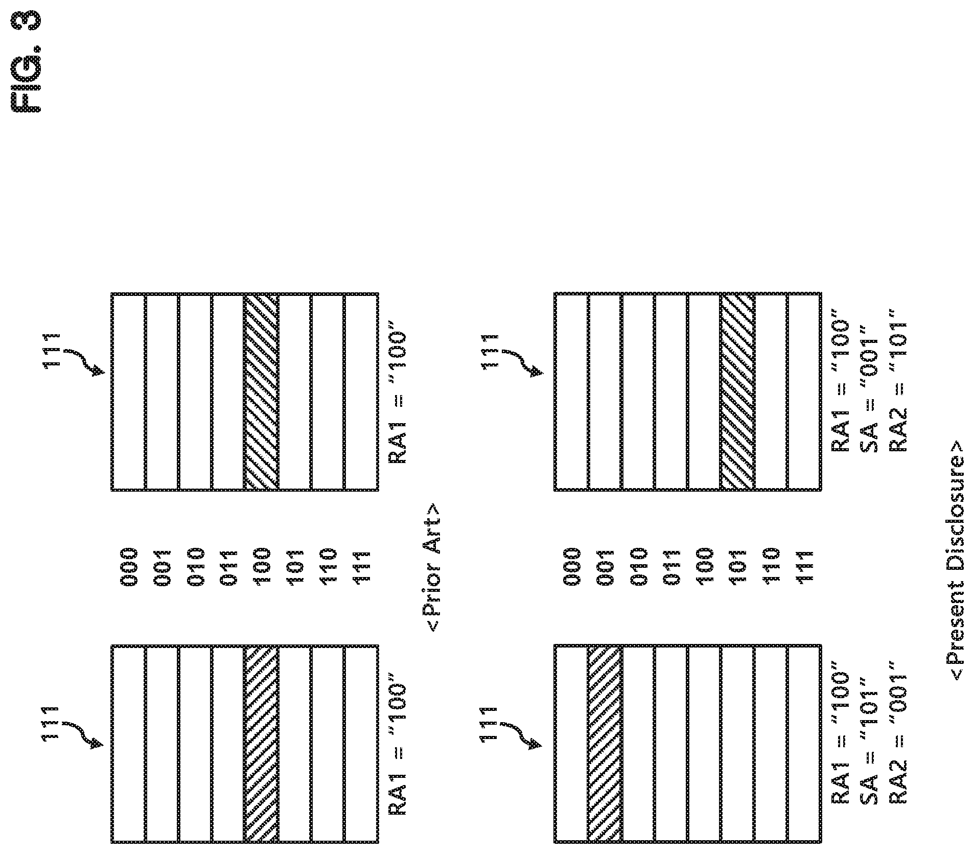
FIG. 3 shows a diagram illustrating an operation of the address conversion circuit 300.
The upper part of FIG. 3 shows a case where a cell die of the stacked cells dies 111 is identified and accessed with the first address RA1, in accordance with the prior art.
If the first address RA1 obtained by decoding the currently requested address is "100" and the first address RA1 obtained by decoding the next requested address is "100," the same cell die is accessed consecutively, as indicated by the same shaded cell die in the upper part of FIG. 3. When the same cell die is repeatedly accessed, heat can build in the cell die and degrade its performance. Similarly, when neighboring cell dies are consecutively accessed, the later-accessed cell die might be preheated by the previously accessed adjacent cell die. Heat can also be slow to dissipate when it builds up in internal regions of a cell die stack.
The lower part of FIG. 3 shows a case where a cell die of the cell dies 111 is identified and accessed with the second address RA2, in accordance with the present teachings.
The second address RA2 is converted to "001" when the first address RA1 is "100" and the bank address BA provided as the selection data SA is "101."
The second address RA2 is converted to "101" when the first address RA1 is "100" and the bank address BA provided as the selection data SA is "001."
In this way, when an access is determined by the second address RA2, different cell dies may be accessed with a same first address RA1, as indicated by different shaded cell dies in the lower part of FIG. 3.
The example of FIG. 3 shows that even when a host requests reading or writing to the same rank, the request can be processed at a different cell dies when the bank address BA changes. Similarly, when a host requests reading or writing to neighboring cell dies, the request can be processed so that the neither the same cell die nor neighboring cell dies are consecutively accessed.
As a result, the issue of rising temperature in a cell die due to concentrated accesses to the same cell die or neighboring can be mitigated or averted.
The present teachings do not require an additional element to sense temperature for managing the temperature of a cell die.
As described above, the present disclosure can efficiently manage heat generated in a cell die while simplifying the configuration of a semiconductor memory device.
For an embodiment, the present teachings work by internally converting an address identifying a cell die. Therefore, there is no need to change the configuration and operation of other elements, such as the data transfer circuit 130 and the command decoder 122.
Because the thermal management is performed without substantially affecting data I/O operations, the data I/O performance is not lowered as compared with a conventional semiconductor memory device.
In addition, because a semiconductor memory device according to the present disclosure does not require a change of configuration or operation of an external device, such as a host, it is possible to perform the thermal management while using the existing system as it is.
Although various embodiments have been described for illustrative purposes, it will be apparent to those skilled in the art that various changes and modifications may be made to the described embodiments without departing from the spirit and scope of the disclosure as defined by the following claims.
* * * * *
References
D00000
D00001
D00002
D00003
XML
uspto.report is an independent third-party trademark research tool that is not affiliated, endorsed, or sponsored by the United States Patent and Trademark Office (USPTO) or any other governmental organization. The information provided by uspto.report is based on publicly available data at the time of writing and is intended for informational purposes only.
While we strive to provide accurate and up-to-date information, we do not guarantee the accuracy, completeness, reliability, or suitability of the information displayed on this site. The use of this site is at your own risk. Any reliance you place on such information is therefore strictly at your own risk.
All official trademark data, including owner information, should be verified by visiting the official USPTO website at www.uspto.gov. This site is not intended to replace professional legal advice and should not be used as a substitute for consulting with a legal professional who is knowledgeable about trademark law.