Power-based and target-based graphics quality adjustment
Appu , et al. February 2, 2
U.S. patent number 10,909,653 [Application Number 16/515,794] was granted by the patent office on 2021-02-02 for power-based and target-based graphics quality adjustment. This patent grant is currently assigned to Intel Corporation. The grantee listed for this patent is Intel Corporation. Invention is credited to Abhishek R. Appu, Stanley J. Baran, Jill M. Boyce, Hiu-Fai R. Chan, Fangwen Fu, James M. Holland, Altug Koker, Sang-Hee Lee, Atthar H. Mohammed, Sumit Mohan, Jong Dae Oh, Keith W. Rowe, Satya N. Yedidi.


View All Diagrams
| United States Patent | 10,909,653 |
| Appu , et al. | February 2, 2021 |
Power-based and target-based graphics quality adjustment
Abstract
An embodiment of an electronic processing system may include an application processor, persistent storage media communicatively coupled to the application processor, a graphics subsystem communicatively coupled to the application processor, a power budget analyzer to identify a power budget for one or more of the application processor, the persistent storage media, and the graphics subsystem, a target analyzer communicatively coupled to the graphics subsystem to identify a target for the graphics subsystem, and a parameter adjuster to adjust one or more parameters of the graphics subsystem based on one or more of the identified power budget and the identified target.
| Inventors: | Appu; Abhishek R. (El Dorado Hills, CA), Baran; Stanley J. (Elk Grove, CA), Lee; Sang-Hee (Santa Clara, CA), Mohammed; Atthar H. (Folsom, CA), Oh; Jong Dae (Folsom, CA), Chan; Hiu-Fai R. (Rancho Cordova, CA), Boyce; Jill M. (Portland, OR), Fu; Fangwen (Folsom, CA), Yedidi; Satya N. (Roseville, CA), Mohan; Sumit (San Jose, CA), Holland; James M. (Folsom, CA), Rowe; Keith W. (Shingle Springs, CA), Koker; Altug (El Dorado Hills, CA) | ||||||||||
|---|---|---|---|---|---|---|---|---|---|---|---|
| Applicant: |
|
||||||||||
| Assignee: | Intel Corporation (Santa Clara,
CA) |
||||||||||
| Family ID: | 1000005337209 | ||||||||||
| Appl. No.: | 16/515,794 | ||||||||||
| Filed: | July 18, 2019 |
Prior Publication Data
| Document Identifier | Publication Date | |
|---|---|---|
| US 20200005424 A1 | Jan 2, 2020 | |
Related U.S. Patent Documents
| Application Number | Filing Date | Patent Number | Issue Date | ||
|---|---|---|---|---|---|
| 15488569 | Apr 17, 2017 | 10402932 | |||
| Current U.S. Class: | 1/1 |
| Current CPC Class: | G06F 1/3265 (20130101); G09G 5/006 (20130101); G06T 1/60 (20130101); G06T 1/20 (20130101); H04N 19/156 (20141101); G06F 1/3206 (20130101); G09G 2340/0407 (20130101); G06T 2210/52 (20130101); G06F 1/3212 (20130101); G06T 2200/16 (20130101); G09G 2330/021 (20130101); Y02D 10/00 (20180101) |
| Current International Class: | G06T 1/20 (20060101); H04N 19/156 (20140101); G06T 1/60 (20060101); G09G 5/00 (20060101); G06F 1/3206 (20190101); G06F 1/3234 (20190101); G06F 1/3212 (20190101) |
References Cited [Referenced By]
U.S. Patent Documents
| 2005/0213929 | September 2005 | Cheng |
| 2010/0091836 | April 2010 | Jia |
| 2010/0128777 | May 2010 | Garg et al. |
| 2010/0128797 | May 2010 | Dey |
| 2010/0128798 | May 2010 | Choudhury |
| 2010/0201791 | August 2010 | Slavenburg et al. |
| 2011/0085079 | April 2011 | Ruggiero |
| 2011/0211036 | September 2011 | Tran |
| 2011/0248993 | October 2011 | Xu |
| 2012/0050303 | March 2012 | McAllister et al. |
| 2012/0075437 | March 2012 | Slavenburg et al. |
| 2012/0131362 | May 2012 | Lee et al. |
| 2012/0195356 | August 2012 | Yi |
| 2013/0120524 | May 2013 | Zheng |
| 2013/0121563 | May 2013 | Chen et al. |
| 2014/0028679 | January 2014 | Pajak et al. |
| 2014/0028703 | January 2014 | Pajak et al. |
| 2014/0049602 | February 2014 | Zhu et al. |
| 2014/0057714 | February 2014 | Phadake |
| 2014/0062975 | March 2014 | Panvelwala |
| 2014/0071245 | March 2014 | Zhang et al. |
| 2014/0079327 | March 2014 | Diard |
| 2014/0092113 | April 2014 | Petersen et al. |
| 2014/0153635 | June 2014 | Zhang et al. |
| 2014/0184813 | July 2014 | Cohen et al. |
| 2014/0184894 | July 2014 | Motta |
| 2014/0185952 | July 2014 | Cabral |
| 2014/0189399 | July 2014 | Govindaraju |
| 2014/0204101 | July 2014 | Ramadoss |
| 2014/0267222 | September 2014 | Gupta et al. |
| 2014/0270551 | September 2014 | Baranowski et al. |
| 2014/0282751 | September 2014 | Lee et al. |
| 2014/0286390 | September 2014 | Fear |
| 2014/0321732 | October 2014 | Bhat et al. |
| 2014/0327771 | November 2014 | Malachowsky et al. |
| 2014/0347439 | November 2014 | Jia et al. |
| 2014/0354659 | December 2014 | Apodaca |
| 2014/0359324 | December 2014 | Park |
| 2014/0369613 | December 2014 | Avadhanam et al. |
| 2015/0009306 | January 2015 | More |
| 2015/0022636 | January 2015 | Savransky |
| 2015/0036875 | February 2015 | Savransky |
| 2015/0067377 | March 2015 | Park |
| 2015/0103184 | April 2015 | Tracey et al. |
| 2015/0116294 | April 2015 | Kumar |
| 2015/0138065 | May 2015 | Alfieri |
| 2015/0139543 | May 2015 | Stewart |
| 2015/0160709 | June 2015 | Park |
| 2015/0181117 | June 2015 | Park |
| 2015/0208079 | July 2015 | Pore et al. |
| 2015/0221064 | August 2015 | Thomas et al. |
| 2015/0229879 | August 2015 | Vojkovich |
| 2015/0243048 | August 2015 | Kim |
| 2015/0264299 | September 2015 | Leech et al. |
| 2015/0310789 | October 2015 | Heide et al. |
| 2015/0310798 | October 2015 | Heide et al. |
| 2015/0348226 | December 2015 | Vaishampayan |
| 2015/0348509 | December 2015 | Verbeure et al. |
| 2016/0259453 | September 2016 | Colenbrander |
| 2017/0120151 | May 2017 | Relan |
| 2017/0171264 | June 2017 | Salomons |
| 2017/0337900 | November 2017 | Dai et al. |
| 2017/0352325 | December 2017 | Spence et al. |
| 2018/0098083 | April 2018 | McAllister |
| 2018/0120923 | May 2018 | Srinivasan |
| 2008131140 | Jun 2008 | JP | |||
| 2009272702 | Nov 2009 | JP | |||
| 2011031692 | Mar 2011 | WO | |||
Other References
|
Nicholas Wilt, "The CUDA Handbook: A Comprehensive Guide to GPU Programming", 522 pages, Jun. 2013, Addison-Wesley, USA. cited by applicant . Shane Cook, "CUDA Programming: A Developer's Guide to Parallel Computing with GPUs", 591 pages, 2013, Elsevier, USA. cited by applicant . Sullivan et al., "Overview of the High Efficiency Video Coding (HEVC) Standard", IEEE Transactions on Circuits and Systems for Video Technology, Dec. 2012, pp. 1649-1668. cited by applicant . "Overview of the High Efficiency Video Coding (HEVC) Standard", retrieved from blog.csdn/net/fireroll/article/details/9075011, Jun. 11, 2013, 6 pages. cited by applicant . Sharman et al., "Common test conditions", JCT-VC, Jan. 2017, 15 pages. cited by applicant . Aboda et al., "Object RRC (ORTC) API for WebRTC", Draft Community Group Report, Jan. 22, 2015, 100 pages. cited by applicant . Image retrieved from encrypted-tbnagstaticcom/images?q=tbn:ANd9GcQZxIWKq78T-bQHlmYrhoXXcocmsYw- ZfSe-41hMQxjaC1UUAM2h, retrieved on Apr. 3, 2017, 1 page. cited by applicant . European Search Report for European Patent Application No. 18167862.4, dated Jul. 26, 2018, 17 pages. cited by applicant . European Search Report for European Patent Application No. 18167862.4, dated Oct. 30, 2018, 13 pages. cited by applicant . "Temporal layers", retrieved from publications.ortc.org/2015/20150122/3-layer-temporal.png, retrieved on Apr. 3, 2017, 1 page. cited by applicant . Non-Final Office Action for U.S. Appl. No. 15/488,569, dated May 18, 2018, 22 pages. cited by applicant . Final Office Action for U.S. Appl. No. 15/488,569, dated Oct. 31, 2018, 14 pages. cited by applicant . Advisory Action for U.S. Appl. No. 15/488,569, dated Jan. 18, 2019, 5 pages. cited by applicant . Notice of Allowance for U.S. Appl. No. 15/488,569, dated Apr. 18, 2019, 15 pages. cited by applicant. |
Primary Examiner: McCulley; Ryan
Attorney, Agent or Firm: Jordan IP Law, LLC
Claims
What is claimed is:
1. A graphics apparatus, comprising: a power budget analyzer to identify a power budget for a graphics system; a target analyzer to identify a target for the graphics system and determine whether the identified target is a video analytics target or a human viewer; and a parameter adjuster communicatively coupled to the power budget analyzer to: adjust an adjustment range of a quantization parameter based on whether the identified target is the video analytics target or the human viewer.
2. The graphics apparatus of claim 1, wherein the parameter adjuster is further to: compare the identified power budget to a budget threshold; and adjust an image tuning parameter of the graphics system based on the comparison of the identified power budget and the budget threshold.
3. The graphics apparatus of claim 2, wherein the parameter adjuster is further to: adjust a block size of a motion vector search region based on the comparison of the identified power budget and the budget threshold.
4. The apparatus of claim 1, wherein the parameter adjuster is further to adjust one or more encode parameters of the graphics system based on the identified target.
5. A method of adjusting a graphics parameter, comprising: identifying a power budget for a graphics system; identifying a target for the graphics system; determining whether the identified target is a video analytics target or a human viewer; and adjusting an adjustment range of a quantization parameter based on whether the identified target is the video analytics target or the human viewer.
6. At least one non-transitory computer readable medium, comprising a set of instructions, which when executed by a computing device cause the computing device to: identify a power budget for a graphics system; identify a target for the graphics system; determine whether the identified target is a video analytics target or a human viewer; and adjust an adjustment range of a quantization parameter based on whether the identified target is the video analytics target or the human viewer.
Description
CROSS-REFERENCED WITH RELATED APPLICATIONS
This patent application claims benefit to U.S. patent application Ser. No. 15/488,569 filed Apr. 17, 2017.
TECHNICAL FIELD
Embodiments generally relate to data processing and to graphics processing via a graphics processing unit. More particularly, embodiments relate to power-based and target-based graphics quality adjustment.
BACKGROUND
In graphics processing architectures, source devices (e.g., cameras, media players, set top boxes, game consoles, etc.) may encode video content prior to transmission of the video content over a wireless or wired link to a sink device (e.g., display, receiver). Different types of frame encoding schemes may be used to improve coding efficiency (e.g., obtain the best video quality at a specific bitrate). For example, advanced video encoders may select between the use of intra coded frames (I-frames), inter-prediction coded frames (P-frames) and bi-directional inter-prediction coded frames (B-frames), based on factors such as the existence of scene changes. Various settings, parameters, and configurations may be applied to various encode/decode operations.
BRIEF DESCRIPTION OF THE DRAWINGS
The various advantages of the embodiments will become apparent to one skilled in the art by reading the following specification and appended claims, and by referencing the following drawings, in which:
FIG. 1 is a block diagram illustrating a computer system configured to implement one or more aspects of the embodiments described herein;
FIGS. 2A-2D illustrate a parallel processor components, according to an embodiment;
FIGS. 3A-3B are block diagrams of graphics multiprocessors, according to embodiments;
FIGS. 4A-4F illustrate an exemplary architecture in which a plurality of GPUs are communicatively coupled to a plurality of multi-core processors;
FIG. 5 illustrates a graphics processing pipeline, according to an embodiment;
FIG. 6 is a block diagram of an example of an electronic processing system according to an embodiment;
FIG. 7 is a block diagram of an example of a graphics apparatus according to an embodiment;
FIGS. 8A-8C are flowcharts of an example of a method of adjusting a graphics parameter according to an embodiment;
FIG. 8D is an illustrative graph of an example of birtrate versus frame encode time according to an embodiment;
FIGS. 8E to 8F are illustrative diagrams of examples of a frame including image data according to an embodiment;
FIG. 8G is a block diagram of an example of a graphics system according to an embodiment;
FIG. 8H is an illustrative diagram of an example of a block for a motion vector search according to an embodiment;
FIG. 9 is a block diagram of an example of a graphics apparatus according to an embodiment;
FIG. 10A is a flowchart of another example of a method of adjusting a graphics parameter according to an embodiment;
FIGS. 10B to 10E are illustrative diagrams of examples of temporal hierarchy structures according to an embodiment;
FIG. 10F is a block diagram of another example of a graphics apparatus according to an embodiment;
FIG. 11 is a block diagram of an example of a display with a localized backlight capability according to an embodiment;
FIG. 12A is a block diagram of an example of a data processing device according to an embodiment;
FIG. 12B is an illustration of an example of a distance determination according to an embodiment;
FIG. 13 is a block diagram of an example of a layered display architecture according to an embodiment;
FIG. 14 is a block diagram of an example of a display architecture that includes multiple display units according to an embodiment;
FIG. 15 is a block diagram of an example of a cloud-assisted media delivery architecture according to an embodiment;
FIGS. 16-18 are block diagrams of an example of an overview of a data processing system according to an embodiment;
FIG. 19 is a block diagram of an example of a graphics processing engine according to an embodiment;
FIGS. 20-22 are block diagrams of examples of execution units according to an embodiment;
FIG. 23 is a block diagram of an example of a graphics pipeline according to an embodiment;
FIGS. 24A-24B are block diagrams of examples of graphics pipeline programming according to an embodiment;
FIG. 25 is a block diagram of an example of a graphics software architecture according to an embodiment;
FIG. 26 is a block diagram of an example of an intellectual property (IP) core development system according to an embodiment; and
FIG. 27 is a block diagram of an example of a system on a chip integrated circuit according to an embodiment.
DETAILED DESCRIPTION
In the following description, numerous specific details are set forth to provide a more thorough understanding of the present invention. However, it will be apparent to one of skill in the art that the present invention may be practiced without one or more of these specific details. In other instances, well-known features have not been described in order to avoid obscuring the present invention.
System Overview
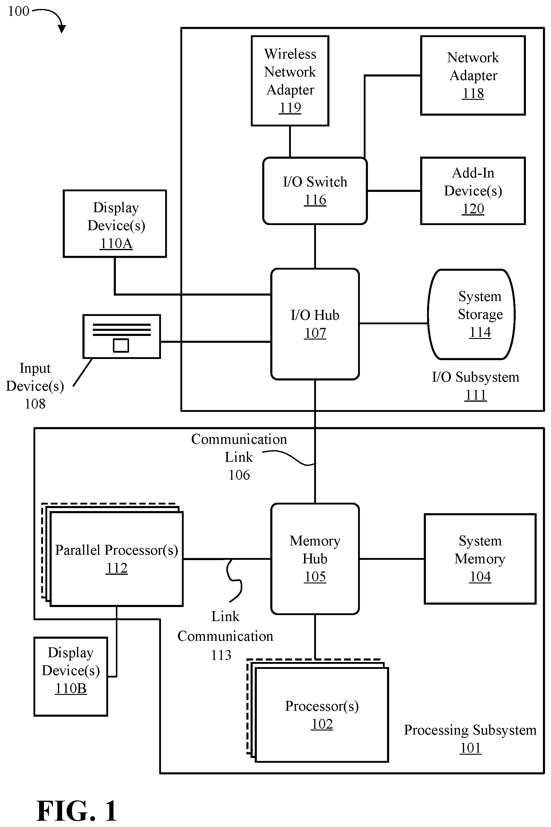
FIG. 1 is a block diagram illustrating a computing system 100 configured to implement one or more aspects of the embodiments described herein. The computing system 100 includes a processing subsystem 101 having one or more processor(s) 102 and a system memory 104 communicating via an interconnection path that may include a memory hub 105. The memory hub 105 may be a separate component within a chipset component or may be integrated within the one or more processor(s) 102. The memory hub 105 couples with an I/O subsystem 111 via a communication link 106. The I/O subsystem 111 includes an I/O hub 107 that can enable the computing system 100 to receive input from one or more input device(s) 108. Additionally, the I/O hub 107 can enable a display controller, which may be included in the one or more processor(s) 102, to provide outputs to one or more display device(s) 110A. In one embodiment the one or more display device(s) 110A coupled with the I/O hub 107 can include a local, internal, or embedded display device.
In one embodiment the processing subsystem 101 includes one or more parallel processor(s) 112 coupled to memory hub 105 via a bus or other communication link 113. The communication link 113 may be one of any number of standards based communication link technologies or protocols, such as, but not limited to PCI Express, or may be a vendor specific communications interface or communications fabric. In one embodiment the one or more parallel processor(s) 112 form a computationally focused parallel or vector processing system that an include a large number of processing cores and/or processing clusters, such as a many integrated core (MIC) processor. In one embodiment the one or more parallel processor(s) 112 form a graphics processing subsystem that can output pixels to one of the one or more display device(s) 110A coupled via the I/O Hub 107. The one or more parallel processor(s) 112 can also include a display controller and display interface (not shown) to enable a direct connection to one or more display device(s) 110B.
Within the I/O subsystem 111, a system storage unit 114 can connect to the I/O hub 107 to provide a storage mechanism for the computing system 100. An I/O switch 116 can be used to provide an interface mechanism to enable connections between the I/O hub 107 and other components, such as a network adapter 118 and/or wireless network adapter 119 that may be integrated into the platform, and various other devices that can be added via one or more add-in device(s) 120. The network adapter 118 can be an Ethernet adapter or another wired network adapter. The wireless network adapter 119 can include one or more of a Wi-Fi, Bluetooth, near field communication (NFC), or other network device that includes one or more wireless radios.
The computing system 100 can include other components not explicitly shown, including USB or other port connections, optical storage drives, video capture devices, and the like, may also be connected to the I/O hub 107. Communication paths interconnecting the various components in FIG. 1 may be implemented using any suitable protocols, such as PCI (Peripheral Component Interconnect) based protocols (e.g., PCI-Express), or any other bus or point-to-point communication interfaces and/or protocol(s), such as the NVLink high-speed interconnect, or interconnect protocols known in the art.
In one embodiment, the one or more parallel processor(s) 112 incorporate circuitry optimized for graphics and video processing, including, for example, video output circuitry, and constitutes a graphics processing unit (GPU). In another embodiment, the one or more parallel processor(s) 112 incorporate circuitry optimized for general purpose processing, while preserving the underlying computational architecture, described in greater detail herein. In yet another embodiment, components of the computing system 100 may be integrated with one or more other system elements on a single integrated circuit. For example, the one or more parallel processor(s), 112 memory hub 105, processor(s) 102, and I/O hub 107 can be integrated into a system on chip (SoC) integrated circuit. Alternatively, the components of the computing system 100 can be integrated into a single package to form a system in package (SIP) configuration. In one embodiment at least a portion of the components of the computing system 100 can be integrated into a multi-chip module (MCM), which can be interconnected with other multi-chip modules into a modular computing system.
It will be appreciated that the computing system 100 shown herein is illustrative and that variations and modifications are possible. The connection topology, including the number and arrangement of bridges, the number of processor(s) 102, and the number of parallel processor(s) 112, may be modified as desired. For instance, in some embodiments, system memory 104 is connected to the processor(s) 102 directly rather than through a bridge, while other devices communicate with system memory 104 via the memory hub 105 and the processor(s) 102. In other alternative topologies, the parallel processor(s) 112 are connected to the I/O hub 107 or directly to one of the one or more processor(s) 102, rather than to the memory hub 105. In other embodiments, the I/O hub 107 and memory hub 105 may be integrated into a single chip. Some embodiments may include two or more sets of processor(s) 102 attached via multiple sockets, which can couple with two or more instances of the parallel processor(s) 112.
Some of the particular components shown herein are optional and may not be included in all implementations of the computing system 100. For example, any number of add-in cards or peripherals may be supported, or some components may be eliminated. Furthermore, some architectures may use different terminology for components similar to those illustrated in FIG. 1. For example, the memory hub 105 may be referred to as a Northbridge in some architectures, while the I/O hub 107 may be referred to as a Southbridge.
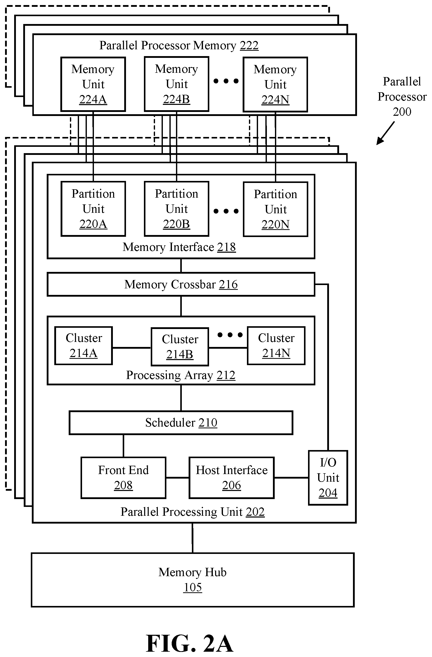
FIG. 2A illustrates a parallel processor 200, according to an embodiment. The various components of the parallel processor 200 may be implemented using one or more integrated circuit devices, such as programmable processors, application specific integrated circuits (ASICs), or field programmable gate arrays (FPGA). The illustrated parallel processor 200 is a variant of the one or more parallel processor(s) 112 shown in FIG. 1, according to an embodiment.
In one embodiment the parallel processor 200 includes a parallel processing unit 202. The parallel processing unit includes an I/O unit 204 that enables communication with other devices, including other instances of the parallel processing unit 202. The I/O unit 204 may be directly connected to other devices. In one embodiment the I/O unit 204 connects with other devices via the use of a hub or switch interface, such as memory hub 105. The connections between the memory hub 105 and the I/O unit 204 form a communication link 113. Within the parallel processing unit 202, the I/O unit 204 connects with a host interface 206 and a memory crossbar 216, where the host interface 206 receives commands directed to performing processing operations and the memory crossbar 216 receives commands directed to performing memory operations.
When the host interface 206 receives a command buffer via the I/O unit 204, the host interface 206 can direct work operations to perform those commands to a front end 208. In one embodiment the front end 208 couples with a scheduler 210, which is configured to distribute commands or other work items to a processing cluster array 212. In one embodiment the scheduler 210 ensures that the processing cluster array 212 is properly configured and in a valid state before tasks are distributed to the processing clusters of the processing cluster array 212. In one embodiment the scheduler 210 is implemented via firmware logic executing on a microcontroller. The microcontroller implemented scheduler 210 is configurable to perform complex scheduling and work distribution operations at coarse and fine granularity, enabling rapid preemption and context switching of threads executing on the processing array 212. In one embodiment, the host software can prove workloads for scheduling on the processing array 212 via one of multiple graphics processing doorbells. The workloads can then be automatically distributed across the processing array 212 by the scheduler 210 logic within the scheduler microcontroller.
The processing cluster array 212 can include up to "N" processing clusters (e.g., cluster 214A, cluster 214B, through cluster 214N). Each cluster 214A-214N of the processing cluster array 212 can execute a large number of concurrent threads. The scheduler 210 can allocate work to the clusters 214A-214N of the processing cluster array 212 using various scheduling and/or work distribution algorithms, which may vary depending on the workload arising for each type of program or computation. The scheduling can be handled dynamically by the scheduler 210, or can be assisted in part by compiler logic during compilation of program logic configured for execution by the processing cluster array 212. In one embodiment, different clusters 214A-214N of the processing cluster array 212 can be allocated for processing different types of programs or for performing different types of computations.
The processing cluster array 212 can be configured to perform various types of parallel processing operations. In one embodiment the processing cluster array 212 is configured to perform general-purpose parallel compute operations. For example, the processing cluster array 212 can include logic to execute processing tasks including filtering of video and/or audio data, performing modeling operations, including physics operations, and performing data transformations.
In one embodiment the processing cluster array 212 is configured to perform parallel graphics processing operations. In embodiments in which the parallel processor 200 is configured to perform graphics processing operations, the processing cluster array 212 can include additional logic to support the execution of such graphics processing operations, including, but not limited to texture sampling logic to perform texture operations, as well as tessellation logic and other vertex processing logic. Additionally, the processing cluster array 212 can be configured to execute graphics processing related shader programs such as, but not limited to vertex shaders, tessellation shaders, geometry shaders, and pixel shaders. The parallel processing unit 202 can transfer data from system memory via the I/O unit 204 for processing. During processing the transferred data can be stored to on-chip memory (e.g., parallel processor memory 222) during processing, then written back to system memory.
In one embodiment, when the parallel processing unit 202 is used to perform graphics processing, the scheduler 210 can be configured to divide the processing workload into approximately equal sized tasks, to better enable distribution of the graphics processing operations to multiple clusters 214A-214N of the processing cluster array 212. In some embodiments, portions of the processing cluster array 212 can be configured to perform different types of processing. For example a first portion may be configured to perform vertex shading and topology generation, a second portion may be configured to perform tessellation and geometry shading, and a third portion may be configured to perform pixel shading or other screen space operations, to produce a rendered image for display. Intermediate data produced by one or more of the clusters 214A-214N may be stored in buffers to allow the intermediate data to be transmitted between clusters 214A-214N for further processing.
During operation, the processing cluster array 212 can receive processing tasks to be executed via the scheduler 210, which receives commands defining processing tasks from front end 208. For graphics processing operations, processing tasks can include indices of data to be processed, e.g., surface (patch) data, primitive data, vertex data, and/or pixel data, as well as state parameters and commands defining how the data is to be processed (e.g., what program is to be executed). The scheduler 210 may be configured to fetch the indices corresponding to the tasks or may receive the indices from the front end 208. The front end 208 can be configured to ensure the processing cluster array 212 is configured to a valid state before the workload specified by incoming command buffers (e.g., batch-buffers, push buffers, etc.) is initiated.
Each of the one or more instances of the parallel processing unit 202 can couple with parallel processor memory 222. The parallel processor memory 222 can be accessed via the memory crossbar 216, which can receive memory requests from the processing cluster array 212 as well as the I/O unit 204. The memory crossbar 216 can access the parallel processor memory 222 via a memory interface 218. The memory interface 218 can include multiple partition units (e.g., partition unit 220A, partition unit 220B, through partition unit 220N) that can each couple to a portion (e.g., memory unit) of parallel processor memory 222. In one implementation the number of partition units 220A-220N is configured to be equal to the number of memory units, such that a first partition unit 220A has a corresponding first memory unit 224A, a second partition unit 220B has a corresponding memory unit 224B, and an Nth partition unit 220N has a corresponding Nth memory unit 224N. In other embodiments, the number of partition units 220A-220N may not be equal to the number of memory devices.
In various embodiments, the memory units 224A-224N can include various types of memory devices, including dynamic random access memory (DRAM) or graphics random access memory, such as synchronous graphics random access memory (SGRAM), including graphics double data rate (GDDR) memory. In one embodiment, the memory units 224A-224N may also include 3D stacked memory, including but not limited to high bandwidth memory (HBM). Persons skilled in the art will appreciate that the specific implementation of the memory units 224A-224N can vary, and can be selected from one of various conventional designs. Render targets, such as frame buffers or texture maps may be stored across the memory units 224A-224N, allowing partition units 220A-220N to write portions of each render target in parallel to efficiently use the available bandwidth of parallel processor memory 222. In some embodiments, a local instance of the parallel processor memory 222 may be excluded in favor of a unified memory design that utilizes system memory in conjunction with local cache memory.
In one embodiment, any one of the clusters 214A-214N of the processing cluster array 212 can process data that will be written to any of the memory units 224A-224N within parallel processor memory 222. The memory crossbar 216 can be configured to transfer the output of each cluster 214A-214N to any partition unit 220A-220N or to another cluster 214A-214N, which can perform additional processing operations on the output. Each cluster 214A-214N can communicate with the memory interface 218 through the memory crossbar 216 to read from or write to various external memory devices. In one embodiment the memory crossbar 216 has a connection to the memory interface 218 to communicate with the I/O unit 204, as well as a connection to a local instance of the parallel processor memory 222, enabling the processing units within the different processing clusters 214A-214N to communicate with system memory or other memory that is not local to the parallel processing unit 202. In one embodiment the memory crossbar 216 can use virtual channels to separate traffic streams between the clusters 214A-214N and the partition units 220A-220N.
While a single instance of the parallel processing unit 202 is illustrated within the parallel processor 200, any number of instances of the parallel processing unit 202 can be included. For example, multiple instances of the parallel processing unit 202 can be provided on a single add-in card, or multiple add-in cards can be interconnected. The different instances of the parallel processing unit 202 can be configured to inter-operate even if the different instances have different numbers of processing cores, different amounts of local parallel processor memory, and/or other configuration differences. For example and in one embodiment, some instances of the parallel processing unit 202 can include higher precision floating point units relative to other instances. Systems incorporating one or more instances of the parallel processing unit 202 or the parallel processor 200 can be implemented in a variety of configurations and form factors, including but not limited to desktop, laptop, or handheld personal computers, servers, workstations, game consoles, and/or embedded systems.
FIG. 2B is a block diagram of a partition unit 220, according to an embodiment. In one embodiment the partition unit 220 is an instance of one of the partition units 220A-220N of FIG. 2A. As illustrated, the partition unit 220 includes an L2 cache 221, a frame buffer interface 225, and a ROP 226 (raster operations unit). The L2 cache 221 is a read/write cache that is configured to perform load and store operations received from the memory crossbar 216 and ROP 226. Read misses and urgent write-back requests are output by L2 cache 221 to frame buffer interface 225 for processing. Updates can also be sent to the frame buffer via the frame buffer interface 225 for processing. In one embodiment the frame buffer interface 225 interfaces with one of the memory units in parallel processor memory, such as the memory units 224A-224N of FIG. 2 (e.g., within parallel processor memory 222).
In graphics applications, the ROP 226 is a processing unit that performs raster operations such as stencil, z test, blending, and the like. The ROP 226 then outputs processed graphics data that is stored in graphics memory. In some embodiments the ROP 226 includes compression logic to compress depth or color data that is written to memory and decompress depth or color data that is read from memory. The compression logic can be lossless compression logic that makes use of one or more of multiple compression algorithms. The type of compression that is performed by the ROP 226 can vary based on the statistical characteristics of the data to be compressed. For example, in one embodiment, delta color compression is performed on depth and color data on a per-tile basis.
In some embodiments, the ROP 226 is included within each processing cluster (e.g., cluster 214A-214N of FIG. 2) instead of within the partition unit 220. In such embodiment, read and write requests for pixel data are transmitted over the memory crossbar 216 instead of pixel fragment data. The processed graphics data may be displayed on a display device, such as one of the one or more display device(s) 110 of FIG. 1, routed for further processing by the processor(s) 102, or routed for further processing by one of the processing entities within the parallel processor 200 of FIG. 2A.
FIG. 2C is a block diagram of a processing cluster 214 within a parallel processing unit, according to an embodiment. In one embodiment the processing cluster is an instance of one of the processing clusters 214A-214N of FIG. 2. The processing cluster 214 can be configured to execute many threads in parallel, where the term "thread" refers to an instance of a particular program executing on a particular set of input data. In some embodiments, single-instruction, multiple-data (SIMD) instruction issue techniques are used to support parallel execution of a large number of threads without providing multiple independent instruction units. In other embodiments, single-instruction, multiple-thread (SIMT) techniques are used to support parallel execution of a large number of generally synchronized threads, using a common instruction unit configured to issue instructions to a set of processing engines within each one of the processing clusters. Unlike a SIMD execution regime, where all processing engines typically execute identical instructions, SIMT execution allows different threads to more readily follow divergent execution paths through a given thread program. Persons skilled in the art will understand that a SIMD processing regime represents a functional subset of a SIMT processing regime.
Operation of the processing cluster 214 can be controlled via a pipeline manager 232 that distributes processing tasks to SIMT parallel processors. The pipeline manager 232 receives instructions from the scheduler 210 of FIG. 2 and manages execution of those instructions via a graphics multiprocessor 234 and/or a texture unit 236. The illustrated graphics multiprocessor 234 is an exemplary instance of a SIMT parallel processor. However, various types of SIMT parallel processors of differing architectures may be included within the processing cluster 214. One or more instances of the graphics multiprocessor 234 can be included within a processing cluster 214. The graphics multiprocessor 234 can process data and a data crossbar 240 can be used to distribute the processed data to one of multiple possible destinations, including other shader units. The pipeline manager 232 can facilitate the distribution of processed data by specifying destinations for processed data to be distributed via the data crossbar 240.
Each graphics multiprocessor 234 within the processing cluster 214 can include an identical set of functional execution logic (e.g., arithmetic logic units, load-store units, etc.). The functional execution logic can be configured in a pipelined manner in which new instructions can be issued before previous instructions are complete. The functional execution logic supports a variety of operations including integer and floating point arithmetic, comparison operations, Boolean operations, bit-shifting, and computation of various algebraic functions. In one embodiment the same functional-unit hardware can be leveraged to perform different operations and any combination of functional units may be present.
The instructions transmitted to the processing cluster 214 constitutes a thread. A set of threads executing across the set of parallel processing engines is a thread group. A thread group executes the same program on different input data. Each thread within a thread group can be assigned to a different processing engine within a graphics multiprocessor 234. A thread group may include fewer threads than the number of processing engines within the graphics multiprocessor 234. When a thread group includes fewer threads than the number of processing engines, one or more of the processing engines may be idle during cycles in which that thread group is being processed. A thread group may also include more threads than the number of processing engines within the graphics multiprocessor 234. When the thread group includes more threads than the number of processing engines within the graphics multiprocessor 234 processing can be performed over consecutive clock cycles. In one embodiment multiple thread groups can be executed concurrently on a graphics multiprocessor 234.
In one embodiment the graphics multiprocessor 234 includes an internal cache memory to perform load and store operations. In one embodiment, the graphics multiprocessor 234 can forego an internal cache and use a cache memory (e.g., L1 cache 308) within the processing cluster 214. Each graphics multiprocessor 234 also has access to L2 caches within the partition units (e.g., partition units 220A-220N of FIG. 2) that are shared among all processing clusters 214 and may be used to transfer data between threads. The graphics multiprocessor 234 may also access off-chip global memory, which can include one or more of local parallel processor memory and/or system memory. Any memory external to the parallel processing unit 202 may be used as global memory. Embodiments in which the processing cluster 214 includes multiple instances of the graphics multiprocessor 234 can share common instructions and data, which may be stored in the L1 cache 308.
Each processing cluster 214 may include an MMU 245 (memory management unit) that is configured to map virtual addresses into physical addresses. In other embodiments, one or more instances of the MMU 245 may reside within the memory interface 218 of FIG. 2. The MMU 245 includes a set of page table entries (PTEs) used to map a virtual address to a physical address of a tile (talk more about tiling) and optionally a cache line index. The MMU 245 may include address translation lookaside buffers (TLB) or caches that may reside within the graphics multiprocessor 234 or the L1 cache or processing cluster 214. The physical address is processed to distribute surface data access locality to allow efficient request interleaving among partition units. The cache line index may be used to determine whether a request for a cache line is a hit or miss.
In graphics and computing applications, a processing cluster 214 may be configured such that each graphics multiprocessor 234 is coupled to a texture unit 236 for performing texture mapping operations, e.g., determining texture sample positions, reading texture data, and filtering the texture data. Texture data is read from an internal texture L1 cache (not shown) or in some embodiments from the L1 cache within graphics multiprocessor 234 and is fetched from an L2 cache, local parallel processor memory, or system memory, as needed. Each graphics multiprocessor 234 outputs processed tasks to the data crossbar 240 to provide the processed task to another processing cluster 214 for further processing or to store the processed task in an L2 cache, local parallel processor memory, or system memory via the memory crossbar 216. A preROP 242 (pre-raster operations unit) is configured to receive data from graphics multiprocessor 234, direct data to ROP units, which may be located with partition units as described herein (e.g., partition units 220A-220N of FIG. 2). The preROP 242 unit can perform optimizations for color blending, organize pixel color data, and perform address translations.
It will be appreciated that the core architecture described herein is illustrative and that variations and modifications are possible. Any number of processing units, e.g., graphics multiprocessor 234, texture units 236, preROPs 242, etc., may be included within a processing cluster 214. Further, while only one processing cluster 214 is shown, a parallel processing unit as described herein may include any number of instances of the processing cluster 214. In one embodiment, each processing cluster 214 can be configured to operate independently of other processing clusters 214 using separate and distinct processing units, L1 caches, etc.
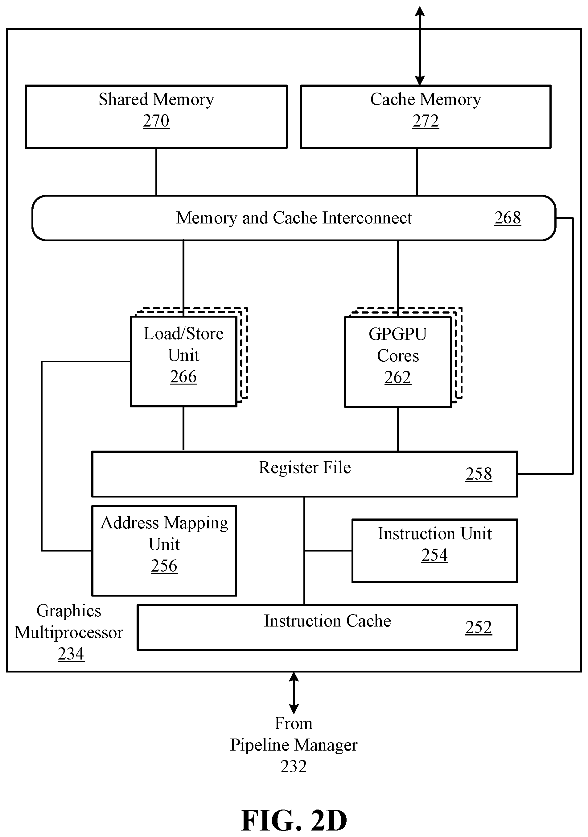
FIG. 2D shows a graphics multiprocessor 234, according to one embodiment. In such embodiment the graphics multiprocessor 234 couples with the pipeline manager 232 of the processing cluster 214. The graphics multiprocessor 234 has an execution pipeline including but not limited to an instruction cache 252, an instruction unit 254, an address mapping unit 256, a register file 258, one or more general purpose graphics processing unit (GPGPU) cores 262, and one or more load/store units 266. The GPGPU cores 262 and load/store units 266 are coupled with cache memory 272 and shared memory 270 via a memory and cache interconnect 268.
In one embodiment, the instruction cache 252 receives a stream of instructions to execute from the pipeline manager 232. The instructions are cached in the instruction cache 252 and dispatched for execution by the instruction unit 254. The instruction unit 254 can dispatch instructions as thread groups (e.g., warps), with each thread of the thread group assigned to a different execution unit within GPGPU core 262. An instruction can access any of a local, shared, or global address space by specifying an address within a unified address space. The address mapping unit 256 can be used to translate addresses in the unified address space into a distinct memory address that can be accessed by the load/store units 266.
The register file 258 provides a set of registers for the functional units of the graphics multiprocessor 324. The register file 258 provides temporary storage for operands connected to the data paths of the functional units (e.g., GPGPU cores 262, load/store units 266) of the graphics multiprocessor 324. In one embodiment, the register file 258 is divided between each of the functional units such that each functional unit is allocated a dedicated portion of the register file 258. In one embodiment, the register file 258 is divided between the different warps being executed by the graphics multiprocessor 324.
The GPGPU cores 262 can each include floating point units (FPUs) and/or integer arithmetic logic units (ALUs) that are used to execute instructions of the graphics multiprocessor 324. The GPGPU cores 262 can be similar in architecture or can differ in architecture, according to embodiments. For example and in one embodiment, a first portion of the GPGPU cores 262 include a single precision FPU and an integer ALU while a second portion of the GPGPU cores include a double precision FPU. In one embodiment the FPUs can implement the IEEE 754-2008 standard for floating point arithmetic or enable variable precision floating point arithmetic. The graphics multiprocessor 324 can additionally include one or more fixed function or special function units to perform specific functions such as copy rectangle or pixel blending operations. In one embodiment one or more of the GPGPU cores can also include fixed or special function logic.
In one embodiment the GPGPU cores 262 include SIMD logic capable of performing a single instruction on multiple sets of data. In one embodiment GPGPU cores 262 can physically execute SIMD4, SIMD8, and SIMD16 instructions and logically execute SIMD1, SIMD2, and SIMD32 instructions. The SIMD instructions for the GPGPU cores can be generated at compile time by a shader compiler or automatically generated when executing programs written and compiled for single program multiple data (SPMD) or SIMT architectures. Multiple threads of a program configured for the SIMT execution model can executed via a single SIMD instruction. For example and in one embodiment, eight SIMT threads that perform the same or similar operations can be executed in parallel via a single SIMD8 logic unit.
The memory and cache interconnect 268 is an interconnect network that connects each of the functional units of the graphics multiprocessor 324 to the register file 258 and to the shared memory 270. In one embodiment, the memory and cache interconnect 268 is a crossbar interconnect that allows the load/store unit 266 to implement load and store operations between the shared memory 270 and the register file 258. The register file 258 can operate at the same frequency as the GPGPU cores 262, thus data transfer between the GPGPU cores 262 and the register file 258 is very low latency. The shared memory 270 can be used to enable communication between threads that execute on the functional units within the graphics multiprocessor 234. The cache memory 272 can be used as a data cache for example, to cache texture data communicated between the functional units and the texture unit 236. The shared memory 270 can also be used as a program managed cached. Threads executing on the GPGPU cores 262 can programmatically store data within the shared memory in addition to the automatically cached data that is stored within the cache memory 272.
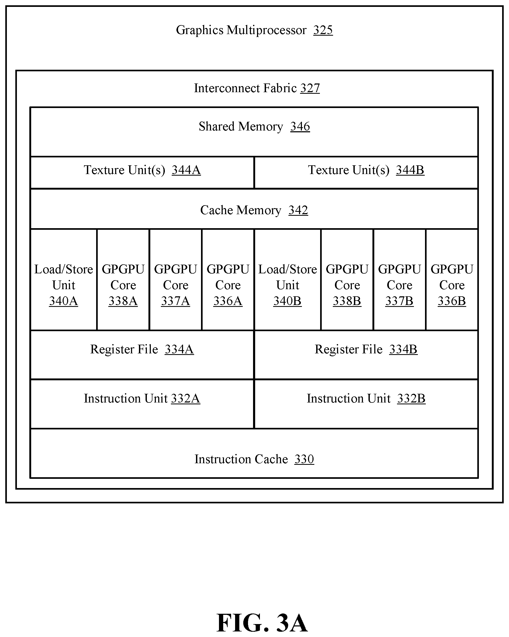
FIGS. 3A-3B illustrate additional graphics multiprocessors, according to embodiments. The illustrated graphics multiprocessors 325, 350 are variants of the graphics multiprocessor 234 of FIG. 2C. The illustrated graphics multiprocessors 325, 350 can be configured as a streaming multiprocessor (SM) capable of simultaneous execution of a large number of execution threads.
FIG. 3A shows a graphics multiprocessor 325 according to an additional embodiment. The graphics multiprocessor 325 includes multiple additional instances of execution resource units relative to the graphics multiprocessor 234 of FIG. 2D. For example, the graphics multiprocessor 325 can include multiple instances of the instruction unit 332A-332B, register file 334A-334B, and texture unit(s) 344A-344B. The graphics multiprocessor 325 also includes multiple sets of graphics or compute execution units (e.g., GPGPU core 336A-336B, GPGPU core 337A-337B, GPGPU core 338A-338B) and multiple sets of load/store units 340A-340B. In one embodiment the execution resource units have a common instruction cache 330, texture and/or data cache memory 342, and shared memory 346.
The various components can communicate via an interconnect fabric 327. In one embodiment the interconnect fabric 327 includes one or more crossbar switches to enable communication between the various components of the graphics multiprocessor 325. In one embodiment the interconnect fabric 327 is a separate, high-speed network fabric layer upon which each component of the graphics multiprocessor 325 is stacked. The components of the graphics multiprocessor 325 communicate with remote components via the interconnect fabric 327. For example, the GPGPU cores 336A-336B, 337A-337B, and 3378A-338B can each communicate with shared memory 346 via the interconnect fabric 327. The interconnect fabric 327 can arbitrate communication within the graphics multiprocessor 325 to ensure a fair bandwidth allocation between components.
FIG. 3B shows a graphics multiprocessor 350 according to an additional embodiment. The graphics processor includes multiple sets of execution resources 356A-356D, where each set of execution resource includes multiple instruction units, register files, GPGPU cores, and load store units, as illustrated in FIG. 2D and FIG. 3A. The execution resources 356A-356D can work in concert with texture unit(s) 360A-360D for texture operations, while sharing an instruction cache 354, and shared memory 362. In one embodiment the execution resources 356A-356D can share an instruction cache 354 and shared memory 362, as well as multiple instances of a texture and/or data cache memory 358A-358B. The various components can communicate via an interconnect fabric 352 similar to the interconnect fabric 327 of FIG. 3A.
Persons skilled in the art will understand that the architecture described in FIGS. 1, 2A-2D, and 3A-3B are descriptive and not limiting as to the scope of the present embodiments. Thus, the techniques described herein may be implemented on any properly configured processing unit, including, without limitation, one or more mobile application processors, one or more desktop or server central processing units (CPUs) including multi-core CPUs, one or more parallel processing units, such as the parallel processing unit 202 of FIG. 2, as well as one or more graphics processors or special purpose processing units, without departure from the scope of the embodiments described herein.
In some embodiments a parallel processor or GPGPU as described herein is communicatively coupled to host/processor cores to accelerate graphics operations, machine-learning operations, pattern analysis operations, and various general purpose GPU (GPGPU) functions. The GPU may be communicatively coupled to the host processor/cores over a bus or other interconnect (e.g., a high speed interconnect such as PCIe or NVLink). In other embodiments, the GPU may be integrated on the same package or chip as the cores and communicatively coupled to the cores over an internal processor bus/interconnect (i.e., internal to the package or chip). Regardless of the manner in which the GPU is connected, the processor cores may allocate work to the GPU in the form of sequences of commands/instructions contained in a work descriptor. The GPU then uses dedicated circuitry/logic for efficiently processing these commands/instructions.
Techniques for GPU to Host Processor Interconnection
FIG. 4A illustrates an exemplary architecture in which a plurality of GPUs 410-413 are communicatively coupled to a plurality of multi-core processors 405-406 over high-speed links 440-443 (e.g., buses, point-to-point interconnects, etc.). In one embodiment, the high-speed links 440-443 support a communication throughput of 4 GB/s, 30 GB/s, 80 GB/s or higher, depending on the implementation. Various interconnect protocols may be used including, but not limited to, PCIe 4.0 or 5.0 and NVLink 2.0. However, the underlying principles of the invention are not limited to any particular communication protocol or throughput.
In addition, in one embodiment, two or more of the GPUs 410-413 are interconnected over high-speed links 444-445, which may be implemented using the same or different protocols/links than those used for high-speed links 440-443. Similarly, two or more of the multi-core processors 405-406 may be connected over high speed link 433 which may be symmetric multi-processor (SMP) buses operating at 20 GB/s, 30 GB/s, 120 GB/s or higher. Alternatively, all communication between the various system components shown in FIG. 4A may be accomplished using the same protocols/links (e.g., over a common interconnection fabric). As mentioned, however, the underlying principles of the invention are not limited to any particular type of interconnect technology.
In one embodiment, each multi-core processor 405-406 is communicatively coupled to a processor memory 401-402, via memory interconnects 430-431, respectively, and each GPU 410-413 is communicatively coupled to GPU memory 420-423 over GPU memory interconnects 450-453, respectively. The memory interconnects 430-431 and 450-453 may utilize the same or different memory access technologies. By way of example, and not limitation, the processor memories 401-402 and GPU memories 420-423 may be volatile memories such as dynamic random access memories (DRAMs) (including stacked DRAMs), Graphics DDR SDRAM (GDDR) (e.g., GDDR5, GDDR6), or High Bandwidth Memory (HBM) and/or may be non-volatile memories such as 3D XPoint or Nano-Ram. In one embodiment, some portion of the memories may be volatile memory and another portion may be non-volatile memory (e.g., using a two-level memory (2LM) hierarchy).
As described below, although the various processors 405-406 and GPUs 410-413 may be physically coupled to a particular memory 401-402, 420-423, respectively, a unified memory architecture may be implemented in which the same virtual system address space (also referred to as the "effective address" space) is distributed among all of the various physical memories. For example, processor memories 401-402 may each comprise 64 GB of the system memory address space and GPU memories 420-423 may each comprise 32 GB of the system memory address space (resulting in a total of 256 GB addressable memory in this example).
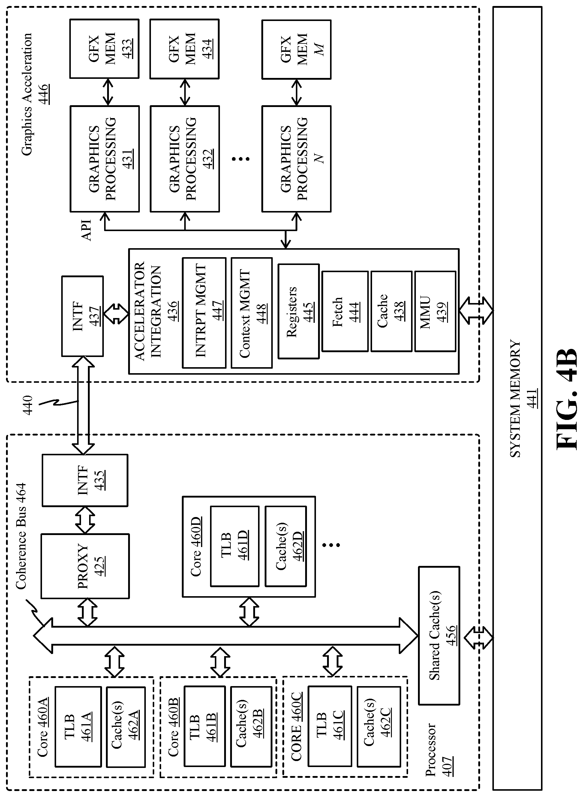
FIG. 4B illustrates additional details for an interconnection between a multi-core processor 407 and a graphics acceleration module 446 in accordance with one embodiment. The graphics acceleration module 446 may include one or more GPU chips integrated on a line card which is coupled to the processor 407 via the high-speed link 440. Alternatively, the graphics acceleration module 446 may be integrated on the same package or chip as the processor 407.
The illustrated processor 407 includes a plurality of cores 460A-460D, each with a translation lookaside buffer 461A-461D and one or more caches 462A-462D. The cores may include various other components for executing instructions and processing data which are not illustrated to avoid obscuring the underlying principles of the invention (e.g., instruction fetch units, branch prediction units, decoders, execution units, reorder buffers, etc.). The caches 462A-462D may comprise level 1 (L1) and level 2 (L2) caches. In addition, one or more shared caches 426 may be included in the caching hierarchy and shared by sets of the cores 460A-460D. For example, one embodiment of the processor 407 includes 24 cores, each with its own L1 cache, twelve shared L2 caches, and twelve shared L3 caches. In this embodiment, one of the L2 and L3 caches are shared by two adjacent cores. The processor 407 and the graphics accelerator integration module 446 connect with system memory 441, which may include processor memories 401-402
Coherency is maintained for data and instructions stored in the various caches 462A-462D, 456 and system memory 441 via inter-core communication over a coherence bus 464. For example, each cache may have cache coherency logic/circuitry associated therewith to communicate to over the coherence bus 464 in response to detected reads or writes to particular cache lines. In one implementation, a cache snooping protocol is implemented over the coherence bus 464 to snoop cache accesses. Cache snooping/coherency techniques are well understood by those of skill in the art and will not be described in detail here to avoid obscuring the underlying principles of the invention.
In one embodiment, a proxy circuit 425 communicatively couples the graphics acceleration module 446 to the coherence bus 464, allowing the graphics acceleration module 446 to participate in the cache coherence protocol as a peer of the cores. In particular, an interface 435 provides connectivity to the proxy circuit 425 over high-speed link 440 (e.g., a PCIe bus, NVLink, etc.) and an interface 437 connects the graphics acceleration module 446 to the link 440.
In one implementation, an accelerator integration circuit 436 provides cache management, memory access, context management, and interrupt management services on behalf of a plurality of graphics processing engines 431, 432, N of the graphics acceleration module 446. The graphics processing engines 431, 432, N may each comprise a separate graphics processing unit (GPU). Alternatively, the graphics processing engines 431, 432, N may comprise different types of graphics processing engines within a GPU such as graphics execution units, media processing engines (e.g., video encoders/decoders), samplers, and blit engines. In other words, the graphics acceleration module may be a GPU with a plurality of graphics processing engines 431-432, N or the graphics processing engines 431-432, N may be individual GPUs integrated on a common package, line card, or chip.
In one embodiment, the accelerator integration circuit 436 includes a memory management unit (MMU) 439 for performing various memory management functions such as virtual-to-physical memory translations (also referred to as effective-to-real memory translations) and memory access protocols for accessing system memory 441. The MMU 439 may also include a translation lookaside buffer (TLB) (not shown) for caching the virtual/effective to physical/real address translations. In one implementation, a cache 438 stores commands and data for efficient access by the graphics processing engines 431-432, N. In one embodiment, the data stored in cache 438 and graphics memories 433-434, N is kept coherent with the core caches 462A-462D, 456 and system memory 411. As mentioned, this may be accomplished via proxy circuit 425 which takes part in the cache coherency mechanism on behalf of cache 438 and memories 433-434, N (e.g., sending updates to the cache 438 related to modifications/accesses of cache lines on processor caches 462A-462D, 456 and receiving updates from the cache 438).
A set of registers 445 store context data for threads executed by the graphics processing engines 431-432, N and a context management circuit 448 manages the thread contexts. For example, the context management circuit 448 may perform save and restore operations to save and restore contexts of the various threads during contexts switches (e.g., where a first thread is saved and a second thread is stored so that the second thread can be execute by a graphics processing engine). For example, on a context switch, the context management circuit 448 may store current register values to a designated region in memory (e.g., identified by a context pointer). It may then restore the register values when returning to the context. In one embodiment, an interrupt management circuit 447 receives and processes interrupts received from system devices.
In one implementation, virtual/effective addresses from a graphics processing engine 431 are translated to real/physical addresses in system memory 411 by the MMU 439. One embodiment of the accelerator integration circuit 436 supports multiple (e.g., 4, 8, 16) graphics accelerator modules 446 and/or other accelerator devices. The graphics accelerator module 446 may be dedicated to a single application executed on the processor 407 or may be shared between multiple applications. In one embodiment, a virtualized graphics execution environment is presented in which the resources of the graphics processing engines 431-432, N are shared with multiple applications or virtual machines (VMs). The resources may be subdivided into "slices" which are allocated to different VMs and/or applications based on the processing requirements and priorities associated with the VMs and/or applications.
Thus, the accelerator integration circuit acts as a bridge to the system for the graphics acceleration module 446 and provides address translation and system memory cache services. In addition, the accelerator integration circuit 436 may provide virtualization facilities for the host processor to manage virtualization of the graphics processing engines, interrupts, and memory management.
Because hardware resources of the graphics processing engines 431-432, N are mapped explicitly to the real address space seen by the host processor 407, any host processor can address these resources directly using an effective address value. One function of the accelerator integration circuit 436, in one embodiment, is the physical separation of the graphics processing engines 431-432, N so that they appear to the system as independent units.
As mentioned, in the illustrated embodiment, one or more graphics memories 433-434, M are coupled to each of the graphics processing engines 431-432, N, respectively. The graphics memories 433-434, M store instructions and data being processed by each of the graphics processing engines 431-432, N. The graphics memories 433-434, M may be volatile memories such as DRAMs (including stacked DRAMs), GDDR memory (e.g., GDDR5, GDDR6), or HBM, and/or may be non-volatile memories such as 3D XPoint or Nano-Ram.
In one embodiment, to reduce data traffic over link 440, biasing techniques are used to ensure that the data stored in graphics memories 433-434, M is data which will be used most frequently by the graphics processing engines 431-432, N and preferably not used by the cores 460A-460D (at least not frequently). Similarly, the biasing mechanism attempts to keep data needed by the cores (and preferably not the graphics processing engines 431-432, N) within the caches 462A-462D, 456 of the cores and system memory 411.
FIG. 4C illustrates another embodiment in which the accelerator integration circuit 436 is integrated within the processor 407. In this embodiment, the graphics processing engines 431-432, N communicate directly over the high-speed link 440 to the accelerator integration circuit 436 via interface 437 and interface 435 (which, again, may be utilize any form of bus or interface protocol). The accelerator integration circuit 436 may perform the same operations as those described with respect to FIG. 4B, but potentially at a higher throughput given its close proximity to the coherency bus 462 and caches 462A-462D, 426.
One embodiment supports different programming models including a dedicated-process programming model (no graphics acceleration module virtualization) and shared programming models (with virtualization). The latter may include programming models which are controlled by the accelerator integration circuit 436 and programming models which are controlled by the graphics acceleration module 446.
In one embodiment of the dedicated process model, graphics processing engines 431-432, N are dedicated to a single application or process under a single operating system. The single application can funnel other application requests to the graphics engines 431-432, N, providing virtualization within a VM/partition.
In the dedicated-process programming models, the graphics processing engines 431-432, N, may be shared by multiple VM/application partitions. The shared models require a system hypervisor to virtualize the graphics processing engines 431-432, N to allow access by each operating system. For single-partition systems without a hypervisor, the graphics processing engines 431-432, N are owned by the operating system. In both cases, the operating system can virtualize the graphics processing engines 431-432, N to provide access to each process or application.
For the shared programming model, the graphics acceleration module 446 or an individual graphics processing engine 431-432, N selects a process element using a process handle. In one embodiment, process elements are stored in system memory 411 and are addressable using the effective address to real address translation techniques described herein. The process handle may be an implementation-specific value provided to the host process when registering its context with the graphics processing engine 431-432, N (that is, calling system software to add the process element to the process element linked list). The lower 16-bits of the process handle may be the offset of the process element within the process element linked list.
FIG. 4D illustrates an exemplary accelerator integration slice 490. As used herein, a "slice" comprises a specified portion of the processing resources of the accelerator integration circuit 436. Application effective address space 482 within system memory 411 stores process elements 483. In one embodiment, the process elements 483 are stored in response to GPU invocations 481 from applications 480 executed on the processor 407. A process element 483 contains the process state for the corresponding application 480. A work descriptor (WD) 484 contained in the process element 483 can be a single job requested by an application or may contain a pointer to a queue of jobs. In the latter case, the WD 484 is a pointer to the job request queue in the application's address space 482.
The graphics acceleration module 446 and/or the individual graphics processing engines 431-432, N can be shared by all or a subset of the processes in the system. Embodiments of the invention include an infrastructure for setting up the process state and sending a WD 484 to a graphics acceleration module 446 to start a job in a virtualized environment.
In one implementation, the dedicated-process programming model is implementation-specific. In this model, a single process owns the graphics acceleration module 446 or an individual graphics processing engine 431. Because the graphics acceleration module 446 is owned by a single process, the hypervisor initializes the accelerator integration circuit 436 for the owning partition and the operating system initializes the accelerator integration circuit 436 for the owning process at the time when the graphics acceleration module 446 is assigned.
In operation, a WD fetch unit 491 in the accelerator integration slice 490 fetches the next WD 484 which includes an indication of the work to be done by one of the graphics processing engines of the graphics acceleration module 446. Data from the WD 484 may be stored in registers 445 and used by the MMU 439, interrupt management circuit 447 and/or context management circuit 446 as illustrated. For example, one embodiment of the MMU 439 includes segment/page walk circuitry for accessing segment/page tables 486 within the OS virtual address space 485. The interrupt management circuit 447 may process interrupt events 492 received from the graphics acceleration module 446. When performing graphics operations, an effective address 493 generated by a graphics processing engine 431-432, N is translated to a real address by the MMU 439.
In one embodiment, the same set of registers 445 are duplicated for each graphics processing engine 431-432, N and/or graphics acceleration module 446 and may be initialized by the hypervisor or operating system. Each of these duplicated registers may be included in an accelerator integration slice 490. Exemplary registers that may be initialized by the hypervisor are shown in Table 1.
TABLE-US-00001 TABLE 1 Hypervisor Initialized Registers 1 Slice Control Register 2 Real Address (RA) Scheduled Processes Area Pointer 3 Authority Mask Override Register 4 Interrupt Vector Table Entry Offset 5 Interrupt Vector Table Entry Limit 6 State Register 7 Logical Partition ID 8 Real address (RA) Hypervisor Accelerator Utilization Record Pointer 9 Storage Description Register
Exemplary registers that may be initialized by the operating system are shown in Table 2.
TABLE-US-00002 TABLE 2 Operating System Initialized Registers 1 Process and Thread Identification 2 Effective Address (EA) Context Save/Restore Pointer 3 Virtual Address (VA) Accelerator Utilization Record Pointer 4 Virtual Address (VA) Storage Segment Table Pointer 5 Authority Mask 6 Work descriptor
In one embodiment, each WD 484 is specific to a particular graphics acceleration module 446 and/or graphics processing engine 431-432, N. It contains all the information a graphics processing engine 431-432, N requires to do its work or it can be a pointer to a memory location where the application has set up a command queue of work to be completed.
FIG. 4E illustrates additional details for one embodiment of a shared model. This embodiment includes a hypervisor real address space 498 in which a process element list 499 is stored. The hypervisor real address space 498 is accessible via a hypervisor 496 which virtualizes the graphics acceleration module engines for the operating system 495.
The shared programming models allow for all or a subset of processes from all or a subset of partitions in the system to use a graphics acceleration module 446. There are two programming models where the graphics acceleration module 446 is shared by multiple processes and partitions: time-sliced shared and graphics directed shared.
In this model, the system hypervisor 496 owns the graphics acceleration module 446 and makes its function available to all operating systems 495. For a graphics acceleration module 446 to support virtualization by the system hypervisor 496, the graphics acceleration module 446 may adhere to the following requirements: 1) An application's job request must be autonomous (that is, the state does not need to be maintained between jobs), or the graphics acceleration module 446 must provide a context save and restore mechanism. 2) An application's job request is guaranteed by the graphics acceleration module 446 to complete in a specified amount of time, including any translation faults, or the graphics acceleration module 446 provides the ability to preempt the processing of the job. 3) The graphics acceleration module 446 must be guaranteed fairness between processes when operating in the directed shared programming model.
In one embodiment, for the shared model, the application 480 is required to make an operating system 495 system call with a graphics acceleration module 446 type, a work descriptor (WD), an authority mask register (AMR) value, and a context save/restore area pointer (CSRP). The graphics acceleration module 446 type describes the targeted acceleration function for the system call. The graphics acceleration module 446 type may be a system-specific value. The WD is formatted specifically for the graphics acceleration module 446 and can be in the form of a graphics acceleration module 446 command, an effective address pointer to a user-defined structure, an effective address pointer to a queue of commands, or any other data structure to describe the work to be done by the graphics acceleration module 446. In one embodiment, the AMR value is the AMR state to use for the current process. The value passed to the operating system is similar to an application setting the AMR. If the accelerator integration circuit 436 and graphics acceleration module 446 implementations do not support a User Authority Mask Override Register (UAMOR), the operating system may apply the current UAMOR value to the AMR value before passing the AMR in the hypervisor call. The hypervisor 496 may optionally apply the current Authority Mask Override Register (AMOR) value before placing the AMR into the process element 483. In one embodiment, the CSRP is one of the registers 445 containing the effective address of an area in the application's address space 482 for the graphics acceleration module 446 to save and restore the context state. This pointer is optional if no state is required to be saved between jobs or when a job is preempted. The context save/restore area may be pinned system memory.
Upon receiving the system call, the operating system 495 may verify that the application 480 has registered and been given the authority to use the graphics acceleration module 446. The operating system 495 then calls the hypervisor 496 with the information shown in Table 3.
TABLE-US-00003 TABLE 3 OS to Hypervisor Call Parameters 1 A work descriptor (WD) 2 An Authority Mask Register (AMR) value (potentially masked). 3 An effective address (EA) Context Save/Restore Area Pointer (CSRP) 4 A process ID (PID) and optional thread ID (TID) 5 A virtual address (VA) accelerator utilization record pointer (AURP) 6 The virtual address of the storage segment table pointer (SSTP) 7 A logical interrupt service number (LISN)
Upon receiving the hypervisor call, the hypervisor 496 verifies that the operating system 495 has registered and been given the authority to use the graphics acceleration module 446. The hypervisor 496 then puts the process element 483 into the process element linked list for the corresponding graphics acceleration module 446 type. The process element may include the information shown in Table 4.
TABLE-US-00004 TABLE 4 Process Element Information 1 A work descriptor (WD) 2 An Authority Mask Register (AMR) value (potentially masked). 3 An effective address (EA) Context Save/Restore Area Pointer (CSRP) 4 A process ID (PID) and optional thread ID (TID) 5 A virtual address (VA) accelerator utilization record pointer (AURP) 6 The virtual address of the storage segment table pointer (SSTP) 7 A logical interrupt service number (LISN) 8 Interrupt vector table, derived from the hypervisor call parameters. 9 A state register (SR) value 10 A logical partition ID (LPID) 11 A real address (RA) hypervisor accelerator utilization record pointer 12 The Storage Descriptor Register (SDR)
In one embodiment, the hypervisor initializes a plurality of accelerator integration slice 490 registers 445.
As illustrated in FIG. 4F, one embodiment of the invention employs a unified memory addressable via a common virtual memory address space used to access the physical processor memories 401-402 and GPU memories 420-423. In this implementation, operations executed on the GPUs 410-413 utilize the same virtual/effective memory address space to access the processors memories 401-402 and vice versa, thereby simplifying programmability. In one embodiment, a first portion of the virtual/effective address space is allocated to the processor memory 401, a second portion to the second processor memory 402, a third portion to the GPU memory 420, and so on. The entire virtual/effective memory space (sometimes referred to as the effective address space) is thereby distributed across each of the processor memories 401-402 and GPU memories 420-423, allowing any processor or GPU to access any physical memory with a virtual address mapped to that memory.
In one embodiment, bias/coherence management circuitry 494A-494E within one or more of the MMUs 439A-439E ensures cache coherence between the caches of the host processors (e.g., 405) and the GPUs 410-413 and implements biasing techniques indicating the physical memories in which certain types of data should be stored. While multiple instances of bias/coherence management circuitry 494A-494E are illustrated in FIG. 4F, the bias/coherence circuitry may be implemented within the MMU of one or more host processors 405 and/or within the accelerator integration circuit 436.
One embodiment allows GPU-attached memory 420-423 to be mapped as part of system memory, and accessed using shared virtual memory (SVM) technology, but without suffering the typical performance drawbacks associated with full system cache coherence. The ability to GPU-attached memory 420-423 to be accessed as system memory without onerous cache coherence overhead provides a beneficial operating environment for GPU offload. This arrangement allows the host processor 405 software to setup operands and access computation results, without the overhead of tradition I/O DMA data copies. Such traditional copies involve driver calls, interrupts and memory mapped I/O (MMIO) accesses that are all inefficient relative to simple memory accesses. At the same time, the ability to access GPU attached memory 420-423 without cache coherence overheads can be critical to the execution time of an offloaded computation. In cases with substantial streaming write memory traffic, for example, cache coherence overhead can significantly reduce the effective write bandwidth seen by a GPU 410-413. The efficiency of operand setup, the efficiency of results access, and the efficiency of GPU computation all play a role in determining the effectiveness of GPU offload.
In one implementation, the selection of between GPU bias and host processor bias is driven by a bias tracker data structure. A bias table may be used, for example, which may be a page-granular structure (i.e., controlled at the granularity of a memory page) that includes 1 or 2 bits per GPU-attached memory page. The bias table may be implemented in a stolen memory range of one or more GPU-attached memories 420-423, with or without a bias cache in the GPU 410-413 (e.g., to cache frequently/recently used entries of the bias table). Alternatively, the entire bias table may be maintained within the GPU.
In one implementation, the bias table entry associated with each access to the GPU-attached memory 420-423 is accessed prior the actual access to the GPU memory, causing the following operations. First, local requests from the GPU 410-413 that find their page in GPU bias are forwarded directly to a corresponding GPU memory 420-423. Local requests from the GPU that find their page in host bias are forwarded to the processor 405 (e.g., over a high-speed link as discussed above). In one embodiment, requests from the processor 405 that find the requested page in host processor bias complete the request like a normal memory read. Alternatively, requests directed to a GPU-biased page may be forwarded to the GPU 410-413. The GPU may then transition the page to a host processor bias if it is not currently using the page.
The bias state of a page can be changed either by a software-based mechanism, a hardware-assisted software-based mechanism, or, for a limited set of cases, a purely hardware-based mechanism.
One mechanism for changing the bias state employs an API call (e.g. OpenCL), which, in turn, calls the GPU's device driver which, in turn, sends a message (or enqueues a command descriptor) to the GPU directing it to change the bias state and, for some transitions, perform a cache flushing operation in the host. The cache flushing operation is required for a transition from host processor 405 bias to GPU bias, but is not required for the opposite transition.
In one embodiment, cache coherency is maintained by temporarily rendering GPU-biased pages uncacheable by the host processor 405. To access these pages, the processor 405 may request access from the GPU 410 which may or may not grant access right away, depending on the implementation. Thus, to reduce communication between the processor 405 and GPU 410 it is beneficial to ensure that GPU-biased pages are those which are required by the GPU but not the host processor 405 and vice versa.
Graphics Processing Pipeline
FIG. 5 illustrates a graphics processing pipeline 500, according to an embodiment. In one embodiment a graphics processor can implement the illustrated graphics processing pipeline 500. The graphics processor can be included within the parallel processing subsystems as described herein, such as the parallel processor 200 of FIG. 2, which, in one embodiment, is a variant of the parallel processor(s) 112 of FIG. 1. The various parallel processing systems can implement the graphics processing pipeline 500 via one or more instances of the parallel processing unit (e.g., parallel processing unit 202 of FIG. 2) as described herein. For example, a shader unit (e.g., graphics multiprocessor 234 of FIG. 3) may be configured to perform the functions of one or more of a vertex processing unit 504, a tessellation control processing unit 508, a tessellation evaluation processing unit 512, a geometry processing unit 516, and a fragment/pixel processing unit 524. The functions of data assembler 502, primitive assemblers 506, 514, 518, tessellation unit 510, rasterizer 522, and raster operations unit 526 may also be performed by other processing engines within a processing cluster (e.g., processing cluster 214 of FIG. 3) and a corresponding partition unit (e.g., partition unit 220A-220N of FIG. 2). The graphics processing pipeline 500 may also be implemented using dedicated processing units for one or more functions. In one embodiment, one or more portions of the graphics processing pipeline 500 can be performed by parallel processing logic within a general purpose processor (e.g., CPU). In one embodiment, one or more portions of the graphics processing pipeline 500 can access on-chip memory (e.g., parallel processor memory 222 as in FIG. 2) via a memory interface 528, which may be an instance of the memory interface 218 of FIG. 2.
In one embodiment the data assembler 502 is a processing unit that collects vertex data for surfaces and primitives. The data assembler 502 then outputs the vertex data, including the vertex attributes, to the vertex processing unit 504. The vertex processing unit 504 is a programmable execution unit that executes vertex shader programs, lighting and transforming vertex data as specified by the vertex shader programs. The vertex processing unit 504 reads data that is stored in cache, local or system memory for use in processing the vertex data and may be programmed to transform the vertex data from an object-based coordinate representation to a world space coordinate space or a normalized device coordinate space.
A first instance of a primitive assembler 506 receives vertex attributes from the vertex processing unit 504. The primitive assembler 506 readings stored vertex attributes as needed and constructs graphics primitives for processing by tessellation control processing unit 508. The graphics primitives include triangles, line segments, points, patches, and so forth, as supported by various graphics processing application programming interfaces (APIs).
The tessellation control processing unit 508 treats the input vertices as control points for a geometric patch. The control points are transformed from an input representation from the patch (e.g., the patch's bases) to a representation that is suitable for use in surface evaluation by the tessellation evaluation processing unit 512. The tessellation control processing unit 508 can also compute tessellation factors for edges of geometric patches. A tessellation factor applies to a single edge and quantifies a view-dependent level of detail associated with the edge. A tessellation unit 510 is configured to receive the tessellation factors for edges of a patch and to tessellate the patch into multiple geometric primitives such as line, triangle, or quadrilateral primitives, which are transmitted to a tessellation evaluation processing unit 512. The tessellation evaluation processing unit 512 operates on parameterized coordinates of the subdivided patch to generate a surface representation and vertex attributes for each vertex associated with the geometric primitives.
A second instance of a primitive assembler 514 receives vertex attributes from the tessellation evaluation processing unit 512, reading stored vertex attributes as needed, and constructs graphics primitives for processing by the geometry processing unit 516. The geometry processing unit 516 is a programmable execution unit that executes geometry shader programs to transform graphics primitives received from primitive assembler 514 as specified by the geometry shader programs. In one embodiment the geometry processing unit 516 is programmed to subdivide the graphics primitives into one or more new graphics primitives and calculate parameters used to rasterize the new graphics primitives.
In some embodiments the geometry processing unit 516 can add or delete elements in the geometry stream. The geometry processing unit 516 outputs the parameters and vertices specifying new graphics primitives to primitive assembler 518. The primitive assembler 518 receives the parameters and vertices from the geometry processing unit 516 and constructs graphics primitives for processing by a viewport scale, cull, and clip unit 520. The geometry processing unit 516 reads data that is stored in parallel processor memory or system memory for use in processing the geometry data. The viewport scale, cull, and clip unit 520 performs clipping, culling, and viewport scaling and outputs processed graphics primitives to a rasterizer 522.
The rasterizer 522 can perform depth culling and other depth-based optimizations. The rasterizer 522 also performs scan conversion on the new graphics primitives to generate fragments and output those fragments and associated coverage data to the fragment/pixel processing unit 524. The fragment/pixel processing unit 524 is a programmable execution unit that is configured to execute fragment shader programs or pixel shader programs. The fragment/pixel processing unit 524 transforming fragments or pixels received from rasterizer 522, as specified by the fragment or pixel shader programs. For example, the fragment/pixel processing unit 524 may be programmed to perform operations included but not limited to texture mapping, shading, blending, texture correction and perspective correction to produce shaded fragments or pixels that are output to a raster operations unit 526. The fragment/pixel processing unit 524 can read data that is stored in either the parallel processor memory or the system memory for use when processing the fragment data. Fragment or pixel shader programs may be configured to shade at sample, pixel, tile, or other granularities depending on the sampling rate configured for the processing units.
The raster operations unit 526 is a processing unit that performs raster operations including, but not limited to stencil, z test, blending, and the like, and outputs pixel data as processed graphics data to be stored in graphics memory (e.g., parallel processor memory 222 as in FIG. 2, and/or system memory 104 as in FIG. 1, to be displayed on the one or more display device(s) 110 or for further processing by one of the one or more processor(s) 102 or parallel processor(s) 112. In some embodiments the raster operations unit 526 is configured to compress z or color data that is written to memory and decompress z or color data that is read from memory.
Power-Based and Target-Based Graphics Quality Adjustment Examples
Turning now to FIG. 6, an embodiment of an electronic processing system 600 may include an application processor 611, persistent storage media 612 communicatively coupled to the application processor 611, a graphics subsystem 613 communicatively coupled to the application processor 611, a power budget analyzer 614 communicatively coupled to the application processor 611, the persistent storage media 612, and the graphics subsystem 613 to identify a power budget for one or more of the application processor 611, the persistent storage media 612, and the graphics subsystem 613, a target analyzer 615 communicatively coupled to the graphics subsystem 613 to identify a target for the graphics subsystem 613, and a parameter adjuster 616 to adjust one or more frame process parameters of the graphics subsystem 613 based on one or more of the identified power budget and the identified target. For example, a frame process parameter may include one or more of an encode parameter and a decode parameter. For example, the one or more frame process parameters may include one or more of an image tuning parameter, a bitrate, an image quality parameter, a motion vector search region, a block size, and a complexity parameter. In some embodiments, the identified target may include a video analytics target.
Embodiments of each of the above application processor 611, persistent storage media 612, display subsystem 613, power budget analyzer 614, target analyzer 615, parameter adjuster 616, and other system components may be implemented in hardware, software, or any suitable combination thereof. For example, hardware implementations may include configurable logic such as, for example, programmable logic arrays (PLAs), FPGAs, complex programmable logic devices (CPLDs), or in fixed-functionality logic hardware using circuit technology such as, for example, ASIC, complementary metal oxide semiconductor (CMOS) or transistor-transistor logic (TTL) technology, or any combination thereof. Alternatively, or additionally, these components may be implemented in one or more modules as a set of logic instructions stored in a machine- or computer-readable storage medium such as random access memory (RAM), read only memory (ROM), programmable ROM (PROM), firmware, flash memory, etc., to be executed by a processor or computing device. For example, computer program code to carry out the operations of the components may be written in any combination of one or more operating system applicable/appropriate programming languages, including an object-oriented programming language such as PYTHON, PERL, JAVA, SMALLTALK, C++, C# or the like and conventional procedural programming languages, such as the "C" programming language or similar programming languages.
Power Budget-Based Parameter Adjustment Examples
Turning now to FIG. 7, an embodiment of a graphics apparatus 700 may include a power budget analyzer 721 to identify a power budget for a graphics system, and a parameter adjuster 722 communicatively coupled to the power budget analyzer 721 to adjust one or more frame process parameters of the graphics system based on the identified power budget. For example, the one or more frame process parameters may include one or more of an image tuning parameter, a bitrate, an image quality parameter, a motion vector search region, a block size, and a complexity parameter.
In some embodiments, the parameter adjuster 722 may be configured to compare the identified power budget to a budget threshold, and adjust an image tuning parameter of the graphics system based on the comparison of the identified power budget and the budget threshold. For example, the parameter adjuster 722 may be configured to compare a frame encode time to a budget time threshold, and reduce a bitrate if the frame encode time exceeds the budget time threshold. In some embodiments, the parameter adjuster 722 may be additionally or alternatively configured to adjust a block size of a motion vector search based on the comparison of the identified power budget and the budget threshold.
Some embodiments of the graphics apparatus 700 may further include a target analyzer 723 communicatively coupled to the parameter adjuster 722 to identify a target for the graphics system. The parameter adjuster 722 may be further configured to adjust one or more encode parameters of the graphics system based on the identified target. For example, the identified target may include a video analytics target.
Embodiments of each of the above power budget analyzer 721, parameter adjuster 722, target analyzer 723, and other components of the apparatus 700 may be implemented in hardware, software, or any combination thereof. For example, hardware implementations may include configurable logic such as, for example, PLAs, FPGAs, CPLDs, or in fixed-functionality logic hardware using circuit technology such as, for example, ASIC, CMOS, or TTL technology, or any combination thereof. Alternatively, or additionally, these components may be implemented in one or more modules as a set of logic instructions stored in a machine- or computer-readable storage medium such as RAM, ROM, PROM, firmware, flash memory, etc., to be executed by a processor or computing device. For example, computer program code to carry out the operations of the components may be written in any combination of one or more operating system applicable/appropriate programming languages, including an object-oriented programming language such as PYTHON, PERL, JAVA, SMALLTALK, C++, C# or the like and conventional procedural programming languages, such as the "C" programming language or similar programming languages.
Turning now to FIGS. 8A to 8C, an embodiment of a method 800 of adjusting a graphics parameter may include identifying a power budget for a graphics system at block 831, and adjusting one or more frame process parameters of the graphics system based on the identified power budget at block 832. For example, the one or more frame process parameters may include one or more of an image tuning parameter, a bitrate, an image quality parameter, a motion vector search region, a block size, and a complexity parameter at block 833.
In some embodiments, the method 800 may further include comparing the identified power budget to a budget threshold at block 834, and adjusting an image tuning parameter of the graphics system based on the comparison of the identified power budget and the budget threshold at block 835. For example, the method 800 may include comparing a frame encode time to a budget time threshold at block 836, and reducing a bitrate if the frame encode time exceeds the budget time threshold at block 837. Some embodiments may additionally or alternatively include adjusting a block size of a motion vector search based on the comparison of the identified power budget and the budget threshold at block 838.
Some embodiments of the method 800 may further include identifying a target for the graphics system at block 839, and adjusting one or more encode parameters of the graphics system based on the identified target at block 840. For example, the identified target may include a video analytics target at block 841.
Embodiments of the method 800 may be implemented in a system, apparatus, GPU, or parallel processing unit (PPU) such as, for example, those described herein. More particularly, hardware implementations of the method 800 may include configurable logic such as, for example, PLAs, FPGAs, CPLDs, or in fixed-functionality logic hardware using circuit technology such as, for example, ASIC, CMOS, or TTL technology, or any combination thereof. Alternatively, or additionally, the method 800 may be implemented in one or more modules as a set of logic instructions stored in a machine- or computer-readable storage medium such as RAM, ROM, PROM, firmware, flash memory, etc., to be executed by a processor or computing device. For example, computer program code to carry out the operations of the components may be written in any combination of one or more operating system applicable/appropriate programming languages, including an object-oriented programming language such as PYTHON, PERL, JAVA, SMALLTALK, C++, C# or the like and conventional procedural programming languages, such as the "C" programming language or similar programming languages. For example, the method 800 may be implemented on a computer readable medium as described in connection with Examples 18 to 24 below.
For example, embodiments or portions of the method 800 may be implemented in applications or driver software (e.g. through an API). Other embodiments or portions of the method 800 may be implemented in specialized code (e.g. shaders) to be executed on a GPU. Other embodiments or portions of the method 800 may be implemented in fixed function logic or specialized hardware (e.g. in the GPU).
Image Tuning Parameter Adjustment Examples
Some embodiments may advantageously provide image/video tuning (e.g. block size, complexity, etc.) based on an existing power budget (e.g. changing encode parameters or other video processing). For example, some embodiments may adjust for power budget in an end-client device by providing initial video processing settings for a particular task, monitoring available compute and/or power resources, and switching the processing settings to a less power intensive mode based on available power to complete the particular task. For example, some embodiments may determine an amount of time left in a video being watched and adjust settings accordingly to be able to finish watching the video before battery dies.
An embodiment of a power budget analyzer may include any of a number of techniques to determine the power budget. In some embodiments, the power budget may be determined based on a power mode, user preferences, and/or configuration settings of the system. In some embodiments, the power budget may be determined based on measured, estimated, or predicted overall power utilization. In some embodiments, the power budget may be based on measured, estimated, or predicted overall power capacity. In some embodiments, the power budget may be determined based on measured, estimated, or predicted power consumption for a particular task. In some embodiments, the power budget may be determined based on a combination of the foregoing (e.g. the current power capacity and the predicted power consumed by a particular task in the current power mode).
For example, if a device has wall power, the power budget may be high. If the device is battery powered, the operating system may determine a power mode for the device and the power budget may be determined based on that power mode. For example, a normal power mode indication from the operating system may correspond to a power budget of medium when on battery power (e.g. or a power budget of high based on user preference settings), while a low power mode indication from the operating system may correspond to a power budget of low.
In some embodiments, the power budget analyzer may additionally, or alternatively, use power measurements to determine the power budget. For example, the power budget analyzer may include or receive information from a power monitor to measure a power utilization (e.g. monitoring a device battery). If the power utilization is greater than a threshold value, some embodiments may adjust various processing parameters to reduce quality/complexity (e.g. as compared to current parameters). In addition, or alternatively, if the power utilization is less than a threshold value, some embodiments may adjust various processing parameters to increase quality/complexity (e.g. as compared to current parameters). Some embodiments may support a range of threshold values or a tier of threshold values. For example, some embodiments may determine if the power utilization is less than a first threshold value and greater than a second threshold value and adjust the parameters accordingly.
In addition, or alternatively, the power monitor may measure a power capacity (e.g. a remaining battery life). If the power capacity is less than a threshold value, some embodiments may adjust various processing parameters to reduce quality/complexity (e.g. as compared to current parameters). In addition, or alternatively, if the power capacity is greater than a threshold value, some embodiments may adjust various processing parameters to increase quality/complexity (e.g. as compared to current parameters). Some embodiments may support a range of threshold values or a tier of threshold values. For example, some embodiments may determine if the power capacity is less than a first threshold value and greater than a second threshold value and adjust the parameters accordingly.
An amount of power consumed by a frame may vary based on the work actually being performed. The power utilization may be an independent variable from performance. When it is independent, some embodiments may prioritize power for changing the parameters rather than frame rate or other performance measures. For example, if the power is spiking and the system is running on battery power (e.g. a 6 watt 2-in-1 tablet), rather than continuing at a high power load some embodiments may start dropping performance for less key areas or settings (e.g. by adjusting an encode/decode parameter). In some embodiments, an application, a scheduler, a micro-controller, etc. may provide a desired power budget for a frame or a task to the power budget analyzer. The amount of power consumed by the task may be measured or estimated by the power budget analyzer and the power budget analyzer may compare the consumed power against the desired power budget. The parameter adjuster may then adjust various parameters for a subsequent frame or task based on the results of the comparison. For example, if the consumed power exceeded the desired power budget the parameters may be adjusted to decrease quality/complexity and consequently reduce the power load for a subsequent frame/task. The process may be repeated until the desired power budget is achieved.
In some embodiments, the power budget and/or the consumed power may be determined based on various proxies for power. For example, processing time may have a direct or indirect relationship to power consumption (e.g. less processing time corresponds to less power consumption). CPU and/or GPU utilization may also have a direct or indirect relationship to power consumption. Thermal sensors may provide temperature information which may have a direct or indirect relationship to power consumption (e.g. a thermal design point (TDP) of the system). Other system performance factors/metrics may likewise have a direct or indirect relationship to power consumption. In some embodiments, the processing time, CPU/GPU utilization, temperature, and/or other system metrics may be monitored and utilized to determine the power budget and/or the consumed power (e.g. in addition to or alternative to any actual power measurement).
In accordance with some embodiments, various processing tasks (e.g. before, during, or after encoding) may be adjusted based on the power budget. In a small form factor device, for example, with a low power budget (e.g. or a larger form factor device running low on battery), less power is available. In addition, or alternatively, the system may be partially utilized by other tasks, and less budget may be available for the particular graphics/display task. Advantageously, some embodiments may determine an available power budget and adjust various video processing parameters based on the available power budget (e.g. to make the video processing simpler and/or less power-intensive when the available power budget is low).
Source image/video data may come from a camera, a file, a stream over a network, a game, etc. For example, the source data may include raw data, decoded data, rendered data, or other image data. The source data may go through a processing step before being sent along to the next stage (e.g. transmission, display, further analytics, etc.). For example, the processing step may enhance the quality of the source data, perform some analytics on the source data, perform computer vision on the source data, etc. A set of parameters for various processing operations may be initially set up based on system configuration, user preferences, application or driver configuration/settings, etc. (e.g. an initial block size may be set based on some sort of anticipated end-to-end flow in terms of a selected quality level, total system resources available on a typical case, etc.). Advantageously, some embodiments may adjust those settings/parameters on-the-fly based on the power budget.
One example of a parameter that may be adjusted on-the-fly based on the power budget may include a block size. For example, instead of performing a blend operation such as a Gaussian blur with an 11.times.11 block size, the operation may be performed with a 5.times.5 block size. The 5.times.5 block may be lower quality but is also much faster in terms of compute, such that processing a whole image/frame (e.g. a 4K image) may be faster and use less CPU/GPU resources and less of the available power budget. Advantageously, some embodiments tune the image/video processing up or down on-the-fly based on the available power budget (e.g. which also may be determined on-the-fly).
Another example of a parameter that may be adjusted on-the-fly based on the power budget may include image processing complexity. For example, a number of different algorithms may perform similar processing of an image with various degrees of complexity and corresponding varying degrees of quality or accuracy. Some embodiments may adjust which algorithm is selected to perform the image processing based on the power budget (e.g. or may skip a processing step altogether). For example, if the power budget is high the normal complexity algorithm may be selected, if the power budget is medium a less complex algorithm may be selected, and if the power budget is low the particular type of image processing may be skipped. In one example, the normal complexity algorithm may correspond to a Gaussian blur, while the less complex algorithm may correspond to a mean blur, and skipping the image processing would correspond to no blur applied to the source data. Advantageously, some embodiments may provide a graceful degradation of the quality based on power budget.
Another parameter that may be adjusted on-the-fly based on the power budget may include color or video quality enhancements. For example, an image processor may enhance contrast, saturate colors, etc. Some embodiments may tune parameters such as block size, algorithm complexity, etc. for image enhancement based on the power budget (e.g. adjust the initially selected block size, adjust the selected algorithm, turn the features on/off, etc.). For example, instead of having full on enhancement feature processing, a reduced set may be provided if the power budget is low (e.g. or some enhancements may be turned off).
Another parameter that may adjusted on-the-fly based on the power budget may include an analytics complexity. For example, normal complexity analytics may be able to perform facial recognition (e.g. an identity of a face in an image) while less complex analytics may be able to perform facial detection (e.g. the presence of a face without a corresponding identity). For example, if the power budget is high the normal complexity analytics may be selected, if the power budget is medium the less complex analytics may be selected, and if the power budget is low then no facial recognition/detection may be performed. In addition, or alternatively, other parameters of the analytics may be adjusted. For example, the number of frames or the number of times the analytics is performed per-frame may be adjusted. If the power budget is high, for example, facial recognition may be performed for every frame, while if the power budget is medium then the frequency may be adjusted such that facial recognition may be performed every five frames. If the power budget is high, the analytics may identify/detect up to ten faces, for example, while if the power budget is low, the analytics may be adjusted to identify/detect only one face. For this particular type of analytics, the parameter adjuster may additionally, or alternatively adjust the size of the face identified/detected based on the power budget (e.g. or range of sizes). Those skilled in the art will understand that different types of analytics will have different parameters that may benefit from on-the-fly adjusting of those parameters based on the power budget, in accordance with some embodiments.
Bitrate Parameter Adjustment Examples
Some embodiments may advantageously provide power budget-based bitrate control. For example, some embodiments may utilize frame statistics to improve image quality while maintaining power budget-based bitrate control. Some embodiments may dynamically budget power based on frame encoding time by selecting an initial quantization parameter (QP), encoding a frame with the selected QP, determining a time to process the frame, and increasing the QP for a next frame if the time is greater than a threshold time. In some embodiments, the frame may be divided into a plurality of coding units (CUs) and a time to process one of the CUs with the selected QP may be determined. If the time to process the CU is greater than another threshold time, the QP may be increased for a next one of the plurality of CUs.
Turning now to FIG. 8D, a graph illustrates how for a selected power budget frame encode time may vary with bitrate. Some systems may benefit from maintaining a target frame rate (e.g. 60 frames-per-second (fps)). For the selected power budget, increasing the bitrate may increase quality but may also increase the frame encode time (e.g. the time required to process one frame of source data). If too many frames in succession take too long, the system may not maintain the target frame rate or frames may get dropped. For a selected power budget, some embodiments may advantageously adjust the bitrate based on the frame encode time to maintain a target frame rate. Longer processing time may correspond to increased power consumption, such that the frame encode time may be considered a proxy for the power budget.
Turning now to FIGS. 8E to 8F, a frame 850 may include image data for a scene. The frame 850 may be divided into a plurality of CUs 852. During encode, a QP value may be assigned to each CU 852, which affects the bitrate. For example, the QP value may be between zero (0) and fifty one (51), with the lower QP values corresponding to higher bitrates (e.g. higher quality and longer processing time) and the higher QP values corresponding to lower bitrate (e.g. lower quality and shorter processing time). For a given power budget, some embodiments may advantageously monitor the frame encode time and dynamically change the QP value based on the frame encode time. For example, if the frame encode time is too long the QP value may be increased which consequently reduces the bitrate (e.g. and reduces the subsequent processing time).
In some embodiments, all of the CUs 852 may be dispatched simultaneously to parallel execution units such the frame is essentially all processed at once. Accordingly, the threshold time may be the time for one frame at the target frame rate (e.g. 1 second divided by 60 fps equals about 16 ms per frame; 1/90 fps equals about 12 ms). In this example, if the frame encode time takes longer than 16 ms for the current frame the QP may be increased for the next frame (e.g. or frames) to decrease the frame encode time to maintain the target frame rate. If the current frame took 18 ms to encode, increasing the QP may reduce the encode time for the next frame to 14 ms (or the subsequent two frames to 15 ms), which may put the encoding back on schedule. Likewise, if the frame encode time takes shorter than 16 ms for the current frame the QP may be decreased for the next frame to increase the quality while maintaining the target frame rate. The QP adjustment may be done on a rolling basis or may be done on a set of frames to maintain the target frame rate for that set (e.g. a different set of 60 frames each second).
In some embodiments, only some of the CUs 852 may be dispatched to the executions units for processing. In this example, the threshold time may be adjusted accordingly depending on how many CUs are processed at once. For example, if the frame 850 is divided into 36 CUs which are processed one row at a time (e.g. 6 CUs per row), the threshold time may be about 2.8 ms for a row of CUs for a target frame rate of 60 fps. In this example, the first row of CUs are each assigned a QP value of 10. If the CU encode time takes longer than 2.8 ms for the first row the QP may be increased for the next row (e.g. adjusted to a QP value of 20) to decrease the CU encode time to maintain the target frame rate. Likewise, if the CU encode time takes shorter than 2.8 ms for the current row the QP may be decreased for the next row to increase the quality while maintaining the target frame rate. The QP adjustment may be done on a rolling basis or may be done on a set of CUs to maintain the target frame rate.
Turning now to FIG. 8G, a graphics system 860 may include a source 861 coupled to a forward transformer 862, which is coupled to a quantizer 863. The quantizer 863 may be coupled to an entropy coder 864 and a context adaptive binary automatic coder (CABAC) 865. The system 860 may include a feedback path which includes an inverse quantizer 866 coupled to an output of the forward transformer 862 and an inverse transformer 867 coupled to an output of the inverse quantizer 866. An output of the inverse transformer 867 may be combined with a reference 868 as input to the forward transformer 862. Advantageously, the system 860 may further include a parameter adjuster 869 coupled to the quantizer 863 to adjust the QP value based on a comparison of encode time against a time threshold (e.g. frame encode time, CU encode time, etc.).
The forward transformer 862 may apply a transformation to source pixels. The transformed pixels may be provided to the quantizer 863 to quantize the transformed pixels based on the selected QP value. After the quantization entropy coding and CABAC coding may applied to provide a bitstream. For example, the system may process two (2) bins per clock cycle. For large image sizes (e.g. 4K video), the bitrate may be limited to not exceed the two bins/clock cycle constraint of the system 860. The output bitstream may be written to memory, displayed, transmitted, etc. Advantageously, in some embodiments the parameter adjuster may dynamically adjust the QP on a per-frame or per-processing cycle basis.
Motion Vector Search Parameter Adjustment Examples
Based on power, some embodiments may advantageously adjust a motion vector search to utilize a smaller search size. For example, based on a power budget, some embodiments may change the search region (e.g. which may be programmed by a driver). For example, the motion vector search may be on a smaller span for a lower power budget. Some embodiments may effectively search the motion vector based on the power budget, while limiting the search over all.
In some systems, each of the 16.times.16 pixel block motion vectors may be searched from frame N to N-1. In accordance with some embodiments, the power budget may cause the search to be adjusted to be based on a bigger chunk 64.times.64 pixel block. There may be sixteen (16) 16.times.16 sub-blocks within the 64.times.64 pixel block. Some embodiments may first find the motion vector for the 64.times.64 pixel block, and then may limit the search for the 16 sub-blocks of 16.times.16 pixel blocks to a narrower area centered around the found 64.times.64 motion vector. Advantageously, some embodiments may significantly lower the search time and save several cycles which may otherwise be required during a motion vector search for each 16.times.16 pixel block. In some embodiments, the size of the bigger chunk block may be programmable. For example, instead of hard fixing a 64.times.64 pixel block size, an application, driver, or shader may select a variable block size based on API hints to choose an appropriate pixel block size (e.g. as a start point). For example, for an even lower power budget the block size may be 128.times.128 or for a more relaxed power budget the block size may go down to 32.times.32.
In accordance with some embodiments, a relatively cruder motion vector search may be performed based on a relatively lower power budget. For example, a smaller region may be used rather than a bigger region. Advantageously, some embodiments may reduce the amount of data that is compared.
Turning now to FIG. 8H, a block 880 for a motion vector search may be divided into a plurality of sub-blocks (e.g. blocks B.sub.1 through B.sub.16). For example, the block 880 may have a block size of 64.times.64 while each of the sub-blocks may have a block size of 16.times.16. To reduce the amount of data to compare, some embodiments may restrict the motion vector searches. Some embodiments may perform more searches, but processing a 64.times.64 block may be more power hungry than processing a 16.times.16 block because a lower number of pixels are compared.
In some embodiments, a central sub-block (e.g. any of sub-blocks B.sub.6, B.sub.7, B.sub.10, or B.sub.11) may be selected to perform a first, full determination of the motion vector search. The resulting motion vector of the first search may then be used as a starting point for subsequent searches in the block 880. For the remaining fifteen sub-blocks, for example, the search area may be constrained within the motion vector found for the first sub-block (e.g. two sub-blocks to the left and two sub-blocks to the right, without searching the entire region). The first search of a central sub-block may provide a reasonable estimated motion vector for the region. Constraining the search for the remaining sub-blocks within the window of the first estimated motion vector may advantageously reduce the amount of processing required and reduce power consumption.
Target-Based Parameter Adjustment Examples
Turning now to FIG. 9, an embodiment of a graphics apparatus 900 may include a target analyzer 921 to identify a target for a graphics system, and a parameter adjuster 922 communicatively coupled to the target analyzer 921 to adjust one or more frame process parameters of the graphics system based on the identified target. For example, the identified target may include a video analytics target. In some embodiments, the parameter adjuster 922 may be configured to increase an adjustment range of a quantization parameter when the identified target corresponds to the video analytics target as compared to the adjustment range of the quantization parameter when the identified target corresponds to a human viewer.
Some embodiments of the graphics apparatus 900 may further include a memory 923 communicatively coupled to the parameter adjuster 922 to store a temporal hierarchy structure. The parameter adjuster 922 may be further configured to assign a first quantization parameter value to a first temporal layer of the temporal hierarchy structure, and assign a second quantization parameter value to a second temporal layer of the temporal hierarchy structure. For example, a difference between the first quantization parameter value and the second quantization parameter value may be greater when the identified target corresponds to the video analytics target as compared to when the identified target corresponds to a human viewer.
Embodiments of each of the above target analyzer 921, parameter adjuster 922, memory 923, and other components of the apparatus 900 may be implemented in hardware, software, or any combination thereof. For example, hardware implementations may include configurable logic such as, for example, PLAs, FPGAs, CPLDs, or in fixed-functionality logic hardware using circuit technology such as, for example, ASIC, CMOS, or TTL technology, or any combination thereof. Alternatively, or additionally, these components may be implemented in one or more modules as a set of logic instructions stored in a machine- or computer-readable storage medium such as RAM, ROM, PROM, firmware, flash memory, etc., to be executed by a processor or computing device. For example, computer program code to carry out the operations of the components may be written in any combination of one or more operating system applicable/appropriate programming languages, including an object-oriented programming language such as PYTHON, PERL, JAVA, SMALLTALK, C++, C# or the like and conventional procedural programming languages, such as the "C" programming language or similar programming languages.
Turning now to FIG. 10A, an embodiment of a method 1000 of adjusting a graphics parameter may include identifying a target for a graphics system at block 1031, and adjusting one or more frame process parameters of the graphics system based on the identified target at block 1032. For example, a frame process parameter may include one or more of an encode parameter and a decode parameter. For example, the identified target may include a video analytics target at block 1033. Some embodiments of the method 1000 may further include increasing an adjustment range of a quantization parameter when the identified target corresponds to the video analytics target as compared to the adjustment range of the quantization parameter when the identified target corresponds to a human viewer at block 1034.
Some embodiments may additionally or alternatively include assigning a first quantization parameter value to a first temporal layer of a temporal hierarchy structure at block 1035, and assigning a second quantization parameter value to a second temporal layer of the temporal hierarchy structure at block 1036. For example, a difference between the first quantization parameter value and the second quantization parameter value may be greater when the identified target corresponds to the video analytics target as compared to when the identified target corresponds to a human viewer at block 1037.
Embodiments of the method 1000 may be implemented in a system, apparatus, GPU, or parallel processing unit (PPU) such as, for example, those described herein. More particularly, hardware implementations of the method 1000 may include configurable logic such as, for example, PLAs, FPGAs, CPLDs, or in fixed-functionality logic hardware using circuit technology such as, for example, ASIC, CMOS, or TTL technology, or any combination thereof. Alternatively, or additionally, the method 1000 may be implemented in one or more modules as a set of logic instructions stored in a machine- or computer-readable storage medium such as RAM, ROM, PROM, firmware, flash memory, etc., to be executed by a processor or computing device. For example, computer program code to carry out the operations of the components may be written in any combination of one or more operating system applicable/appropriate programming languages, including an object-oriented programming language such as PYTHON, PERL, JAVA, SMALLTALK, C++, C# or the like and conventional procedural programming languages, such as the "C" programming language or similar programming languages. For example, the method 1000 may be implemented on a computer readable medium as described in connection with Examples 40 to 43 below.
For example, embodiments or portions of the method 1000 may be implemented in applications or driver software (e.g. through an API). Other embodiments or portions of the method 1000 may be implemented in specialized code (e.g. shaders) to be executed on a GPU. Other embodiments or portions of the method 1000 may be implemented in fixed function logic or specialized hardware (e.g. in the GPU).
Without being limited to theory of operation, generally with video coding/decoding there may be various trade-offs between quality and processing resources on a per-frame basis. For typical video expected to be viewed by humans, some variation in quality between frames (e.g. to save power or due to lack of processing resources) may be acceptable for a good viewing experience but such variation is generally constrained within a range that is less perceptible to humans. An abrupt change in quality between frames may be noticeable to a human viewer, which may negatively impact the viewing experience. Non-human targets, however, may have no issues with abrupt changes in quality between video frames. Various video analytics, for example, may not be intended to be viewed by humans. Non-limiting examples of video analytics may include object detection and/or recognition, motion detection and/or motion tracking, facial detection and/or recognition, gesture detection and/or recognition, etc. Video analytics may analyze a frame to determine the presence of an object, motion of an object, object identification, etc. The frame may be analyzed by a computer as opposed to viewed by a human. Conventional assumptions made to limit variation in quality temporally do not necessarily apply to a non-human target. Advantageously, some embodiments may adjust parameters for a graphics system based on one or more identified targets. Examples of targets may include a human target, an object detection analytics target, an object recognition analytics target, a motion detection analytics target, a motion tracking analytics target, a facial detection analytics target, a facial recognition analytics target, etc.
In accordance with some embodiments, a target analyzer may use any of a number of techniques to identify a target. For example, the target analyzer may analyze system configuration and settings to identify installed components, modules, drivers, libraries, shaders, etc. During runtime, the target analyzer may analyze the loaded components, modules, drivers, library routines, shaders, etc. The target analyzer may be able to determine the source of a request for image/frame data to identify the target. For example, the target analyzer may analyze CPU, GPU, and/or IO transactions to identify the source of a request or the destination for the image/frame data. In some embodiments, the target itself may self-identify to the target analyzer. For example, a handshake communication may occur where the target provides metadata, tag, or other information with identifying characteristics to the target analyzer. In some embodiments, the target may be identified to the target analyzer by an application or driver. For example, an API call may include a variable which identifies the target to the target analyzer.
One way that temporal quality adjustments may be made include adjusting the quantization parameter (QP). For a human target, when adjusting the QP, the amount of adjustment between frames (e.g. sometimes referred to as a QP offset) may be limited to reduce the amount of quality variation between frames. For video analytics, in accordance with some embodiments, the adjustment range may be wider. Some embodiments may assign the QP value differently if the target for a frame is known to be for analytics as opposed to human viewing. Likewise, different types of analytics may have different quality requirements, and the range/QP offset may be determined based on the target analytics. In some embodiments, certain key frames may be kept at high quality (low QP), while intermediate frames have substantially lower quality (high QP), with a QP offset well beyond what may be suitable for a good human viewing experience. Advantageously, some embodiments may dramatically reduce the bitrate while maintaining sufficient video quality for the analytics.
As discussed above, for example, suitable QP values and QP offsets may be different for human targets and non-human targets. Suitable QP values and QP offsets may also be different for different types of video analytics targets. Suitable QP values and QP offsets for facial recognition video analytics, for example, may be different from suitable QP values and QP offsets for motion detection video analytics.
Some systems may support a hierarchical temporal structure, such as a temporal prediction structure. An example temporal prediction structure may have a hierarchy where there are lower temporal layer pictures and higher temporal layer pictures (e.g. a temporal layer 0, a temporal layer 1, a temporal layer 2, etc.). In some embodiments, temporal layer zero may have highest quality for coding, temporal layer one may be lower quality than temporal layer zero, temporal layer two may be lower quality than temporal layer one, etc. In some systems, the QP value may vary between the layers, but in a constrained manner to avoid abrupt changes in encode quality that might be perceptible to a human viewer. Some systems may include a QP offset to define how much the QP value may change between temporal layers.
In accordance with some embodiments, each temporal layer may advantageously have a first QP value for the temporal layer corresponding to a first target and a second QP value for the temporal layer corresponding to a second target, and additional QP values as needed for the temporal layer corresponding to third through Nth targets. Likewise, in some embodiments, each temporal layer may advantageously have a first QP offset for the temporal layer corresponding to a first target and a second QP offset for the temporal layer corresponding to a second target, and additional QP offsets as needed for the temporal layer corresponding to third through Nth targets.
Turning now to FIGS. 10B to 10C, a temporal hierarchy structure 1040 may include a temporal layer 0, a temporal layer 1, through a temporal layer N. A target analyzer may identify the target for the structure 1040 to be a first target (e.g. a human target). A parameter adjuster may set QP values for each of the temporal layers to respective values of 5, 8, and 11 corresponding to suitable values for the first target (see FIG. 10B). If the target analyzer identified or later identifies the target for the structure 1040 to be a second target (e.g. a video analytics target), the parameter adjuster may adjust the QP values for the temporal layers to respective values of 5, 15, and 25 corresponding to suitable values for the second target (see FIG. 10C).
Turning now to FIGS. 10D to 10E, a temporal hierarchy structure 1050 may include a temporal layer 0, a temporal layer 1, through a temporal layer N. A target analyzer may identify the target for the structure 1050 to be a first target (e.g. a human target). A parameter adjuster may set QP offsets for each of the temporal layers to respective values of +/-3, +/-4, and +/-5 corresponding to suitable values for the first target (see FIG. 10D). If the target analyzer identified or later identifies the target for the structure 1050 to be a second target (e.g. a video analytics target), the parameter adjuster may adjust the QP offsets for the temporal layers to respective values of +/-5, +/-10, and +/-15 corresponding to suitable values for the second target (see FIG. 10E).
Turning now to FIG. 10F, a graphics system 1060 may include source image/frame data provided to a local encoder 1062 connected to remote decoder 1063 through a network service 1064 (e.g. a cloud service). A video analytics target 1065 may be communicatively coupled to the remote decoder 1063 to perform video analytics in the decoded data. Some embodiments may advantageously provide temporally varying video quality for remote analytics (e.g. frame by frame variations in video quality). For example, some embodiments may allow much greater variation in temporal quality than might be used for human viewing when targeted for remote video analytics. Some embodiments may utilize much lower QP for some frames (e.g. especially for score change or heavy motion). Advantageously, some embodiments may dramatically reduce bitrate for remote video analytics targets, which may also reduce network bandwidth requirements.
Starting with a reasonable quality key frame, for example, a video analytics target may be able to identify an object. Some embodiments may provide lower quality subsequent frames to the video analytics target to track motion of that object. For example, one frame out of 60 may be good quality while the remaining 59 frames may be much lower quality (but sufficient quality for object tracking). For example, another video analytics target may perform face recognition on the good quality frame and just perform motion recognition of the recognized face for the subsequent lower quality frames. The subsequent lower quality frames may not provide sufficient quality to perform facial recognition of a particular person, but may have enough quality to identify the continued presence of a previously identified face area and relative motion of that identified face area from frame to frame.
In some embodiments, a key frame may correspond to an I-frame, which may occur every 60 frames. The other frames may correspond to P-frames. Some embodiments may have a random-access picture in a stream of frames, which may be better quality, which may correspond to a key frame. For a broadcast signal, for example, a random-access point may start the playback for viewers who tune into the signal at different points in time. An identified scene change may also be a criterion for a change in quality. For example, a first frame after a scene change may be high quality.
Display Technology
Turning now to FIG. 11, a performance-enhanced computing system 1100 is shown. In the illustrated example, a processor 1110 is coupled to a display 1120. The processor 1110 may generally generate images to be displayed on an LCD panel 1150 of the display 1120. In one example, the processor 1110 includes a communication interface such as, for example, a video graphics array (VGA), a DisplayPort (DP) interface, an embedded DisplayPort (eDP) interface, a high-definition multimedia interface (HDMI), a digital visual interface (DVI), and so forth. The processor 1110 may be a graphics processor (e.g., graphics processing unit/GPU) that processes graphics data and generates the images (e.g., video frames, still images) displayed on the LCD panel 1150. Moreover, the processor 1110 may include one or more image processing pipelines that generate pixel data. The image processing pipelines may comply with the OPENGL architecture, or other suitable architecture. Additionally, the processor 1110 may be connected to a host processor (e.g., central processing unit/CPU), wherein the host processor executes one or more device drivers that control and/or interact with the processor 1110.
The illustrated display 1120 includes a timing controller (TCON) 1130, which may individually address different pixels in the LCD panel 1150 and update each individual pixel in the LCD panel 1150 per refresh cycle. In this regard, the LCD panel 1150 may include a plurality of liquid crystal elements such as, for example, a liquid crystal and integrated color filter. Each pixel of the LCD panel 1150 may include a trio of liquid crystal elements with red, green, and blue color filters, respectively. The LCD panel 1150 may arrange the pixels in a two-dimensional (2D) array that is controlled via row drivers 1152 and column drivers 1154 to update the image being displayed by the LCD panel 1150. Thus, the TCON 1130 may drive the row drivers 1152 and the column drivers 1154 to address specific pixels of the LCD panel 1150. The TCON 1130 may also adjust the voltage provided to the liquid crystal elements in the pixel to change the intensity of the light passing through each of the three liquid crystal elements and, therefore, change the color of the pixel displayed on the surface of the LCD panel 1150.
A backlight 1160 may include a plurality of light emitting elements such as, for example, light emitting diodes (LEDs), that are arranged at an edge of the LCD panel 1150. Accordingly, the light generated by the LEDs may be dispersed through the LCD panel 1150 by a diffuser (not shown). In another example, the LEDs are arranged in a 2D array directly behind the LCD panel 1150 in a configuration sometimes referred to as direct backlighting because each LED disperses light through one or more corresponding pixels of the LCD panel 1150 positioned in front of the LED. The light emitting elements may also include compact florescent lamps (CFL's) arranged along one or more edges of the LCD panel 1150. To eliminate multiple edges, the combination of edges may be altered to achieve selective illumination of a region, wherein less than the total set of lighting elements is used with less power.
The light emitting elements may also include one or more sheets of electroluminescent material placed behind the LCD panel 1150. In such a case, light from the surface of the sheet may be dispersed through the pixels of the LCD panel 1150. Additionally, the sheet may be divided into a plurality of regions such as, for example, quadrants. In one example, each region is individually controlled to illuminate only a portion of the LCD panel 1150. Other backlighting solutions may also be used.
The illustrated display 1120 also includes a backlight controller (BLC) 1140 that provides a voltage to the light emitting elements of the backlight 1160. For example, the BLC 1140 may include a pulse width modulation (PWM) driver (not shown) to generate a PWM signal that activates at least a portion of the light emitting elements of the backlight 1160. The duty cycle and frequency of the PWM signal may cause the light generated by the light emitting elements to dim. For example, a 100% duty cycle may correspond to the light emitting elements being fully on and a 0% duty cycle may correspond to the light emitting elements being fully off. Thus, intermediate duty cycles (e.g., 25%, 50%) typically cause the light emitting elements to be turned on for a portion of a cycle period that is proportional to the percentage of the duty cycle. The cycle period of may be fast enough that the blinking of the light emitting elements is not noticeable to the human eye. Moreover, the effect to the user may be that the level of the light emitted by the backlight 1160 is lower than if the backlight 1160 were fully activated. The BLC 1140 may be separate from or incorporated into the TCON 1130.
Alternatively, an emissive display system may be used where the LCD panel 1150 would be replaced by an emissive display panel (e.g. organic light emitting diode/OLED) the backlight 1160 would be omitted, and the row and column drivers 1152 and 1154, respectively, may be used to directly modulate pixel color and brightness.
Distance Based Display Resolution
FIG. 12A shows a scenario in which a user 1218 interacts with a data processing device 1200 containing a display unit 1228. The display processing device 1200 may include, for example, a notebook computer, a desktop computer, a tablet computer, a convertible tablet, a mobile Internet device (MID), a personal digital assistant (PDA), a wearable device (e.g., head mounted display/HMD), a media player, etc., or any combination thereof. The illustrated data processing device 1200 includes a processor 1224 (e.g., embedded controller, microcontroller, host processor, graphics processor) coupled to a memory 1222, which may include storage locations that are addressable through the processor 1224. As will be discussed in greater detail, a distance sensor 1210 may enable distance based display resolution with respect to the display units 1228.
The illustrated memory 1222 includes display data 1226 that is to be rendered on the display unit 1228. In one example, the processor 1224 conducts data conversion on the display data 1226 prior to presenting the display data 1226 on the display unit 1228. A post-processing engine 1214 may execute on the processor 1224 to receive the display data 1226 and an output of the distance sensor 1210. The post-processing engine 1214 may modify the display data 1226 to enhance the readability of screen content on the display unit 1228, reduce power consumption in the data processing device 1200, etc., or any combination thereof.
The illustrated memory 1222 stores a display resolution setting 1216, in addition to an operating system 1212 and an application 1220. The display resolution setting 1216 may specify a number of pixels of the display data 1226 to be presented on the display unit 1228 along a length dimension and a width dimension. If the display data 1226 as generated by the application 1220 is incompatible with the format of the display unit 1228, the processor 1224 may configure the scale of the display data 1226 to match the format of the display units 1228. In this regard, the display resolution setting 1216 may be associated with and/or incorporated into configuration data that defines other settings for the display unit 1228. Moreover, the display resolution setting 1216 may be defined in terms of unit distance or area (e.g., pixels per inch/PPI), or other suitable parameter.
The application 1220 may generate a user interface, wherein the user 1218 may interact with the user interface to select the display resolution setting 1216 from one or more options provided through the user interface, enter the display resolution setting 1216 as a requested value, and so forth. Thus, the display data 1226 may be resized to fit into the display resolution setting 1216 prior to being rendered on the display unit 1228.
The distance sensor 1210 may track the distance between the user 1218 and the display unit 1228, wherein distance sensing may be triggered through a physical button associated with the data processing device 1200/display unit 1228, through the user interface provided by the application 1220 and/or loading of the operating system 1220, and so forth. For example, during a boot of the data processing device 1200 the operating system 1212 may conduct an automatic process to trigger the distance sensing in the background or foreground. Distance sensing may be conducted periodically or continuously.
FIG. 12B shows one example of a distance sensing scenario. In the illustrated example, the distance sensor 1210 uses a transceiver 1208 to emit an electromagnetic beam 1202 in the direction of the user 1218. Thus, the transceiver 1202 might be positioned on a front facing surface of the data processing device 1200 (FIG. 12A). The electromagnetic beam 1202 may impact the user 1218 and be reflected/scattered from the user 1218 as a return electromagnetic beam 1204. The return electromagnetic beam 1204 may be analyzed by, for example, the processor 1224 (FIG. 12A) and/or the post-processing engine 1214 (FIG. 12A) to determine the distance 1206 between the user 1218 and the display unit 1228 (FIG. 12A). The distance 1206 may be used to adjust the display resolution setting 1216.
Display Layers
Turning now to FIG. 13, a display system 1300 is shown in which cascaded display layers 1361, 1362 and 1363 are used to achieve spatial/temporal super-resolution in a display assembly 1360. In the illustrated example, a processor 1310 provides original graphics data 1334 (e.g., video frames, still images), to the system 1300 via a bus 1320. A cascaded display program 1331 may be stored in a memory 1330, wherein the cascaded display program 1331 may be part of a display driver associated with the display assembly 1360. The illustrated memory 1330 also includes the original graphics data 1334 and factorized graphics data 1335. In one example, the cascaded display program 1331 includes a temporal factorization component 1332 and a spatial factorization component 1333. The temporal factorization component 1332 may perform temporal factorization computation and the spatial factorization component may perform spatial factorization computation. The cascaded display program 1331 may derive the factorized graphics data 1335 for presentation on each display layer 1361, 1362 and 1363 based on user configurations and the original graphics data 1334.
The display assembly 1360 may be implemented as an LCD (liquid crystal display) used in, for example, a head mounted display (HMD) application. More particularly, the display assembly 1360 may include a stack of LCD panels interface boards a lens attachment, and so forth. Each panel may be operated at a native resolution of, for example, 1280.times.800 pixels and with a 60 Hz refresh rate. Other native resolutions, refresh rates, display panel technology and/or layer configurations may be used.
Multiple Display Units
FIG. 14 shows a graphics display system 1400 that includes a set of display units 1430 (1430a-1430n) that may generally be used to output a widescreen (e.g., panoramic) presentation 1440 that includes coordinated content in a cohesive and structured topological form. In the illustrated example, a data processing device 1418 includes a processor 1415 that applies a logic function 1424 to hardware profile data 1402 received from the set of display units 1430 over a network 1420. The application of the logic function 1424 to the hardware profile data 1402 may create a set of automatic topology settings 1406 when a match of the hardware profile data with a set of settings in a hardware profile lookup table 1412 is not found. The illustrated set of automatic topology settings 1406 are transmitted from the display processing device 1418 to the display units 1430 over the network 1420.
The processor 1415 may perform and execute the logic function 1424 upon receipt of the logic function 1424 from a display driver 1410. In this regard, the display driver 1410 may include an auto topology module 1408 that automatically configures and structures the topologies of the display units 1432 to create the presentation 1440. In one example, the display driver 1410 is a set of instructions, which when executed by the processor 1415, cause the data processing device 1418 to communicate with the display units 1430, video cards, etc., and conduct automatic topology generation operations.
The data processing device 1418 may include, for example, a server, desktop, notebook computer, tablet computer, convertible tablet, MID, PDA, wearable device, media player, and so forth. Thus, the display processing device 1418 may include a hardware control module 1416, a storage device 1414, random access memory (RAM, not shown), controller cards including one or more video controller cards, and so forth. In one example, the display units 1430 are flat-panel displays (e.g., liquid crystal, active matrix, plasma, etc.), HMD's, video projection devices, and so forth, that coordinate with one another to produce the presentation 1440. Moreover, the presentation 1440 may be generated based on a media file stored in the storage device 1414, wherein the media file might include, for example, a film, video clip, animation, advertisement, etc., or any combination thereof.
The term "topology" may be considered the number, scaling, shape and/or other configuration parameter of a first display unit 1430a, a second display unit 1430b, a third display unit 1430n, and so forth. Accordingly, the topology of the display units 1430 may enable the presentation 1440 be visually presented in concert such that the individual sections of the presentation 1440 are proportional and compatible with the original dimensions and scope of the media being played through the display units 1430. Thus, the topology may constitute spatial relations and/or geometric properties that are not impacted by the continuous change of shape or size of the content rendered in the presentation 1440. In one example, the auto topology module 1408 includes a timing module 1426, a control module 1428, a signal monitor module 1432 and a signal display module 1434. The timing module 1426 may designate a particular display unit in the set of display units 1430 as a sample display unit. In such a case, the timing module 1426 may designate the remaining display units 1430 as additional display units. In one example, the timing module 1426 automatically sets a shaping factor to be compatible with the hardware profile data 1402, wherein the presentation 1440 is automatically initiated by a sequence of graphics signals 1422.
In one example, the control module 1428 modifies the set of automatic topology settings 1406. Additionally, the signal monitor module 1432 may automatically monitor the sequence of graphics signals 1422 and trigger the storage device 1414 to associate the set of automatic topology settings 1406 with the hardware profile lookup table 1412. Moreover, the signal monitor module 1432 may automatically detect changes in the set of display units 1430 according to a set of change criteria and automatically generate a new topology profile corresponding to the change in the set of display units 1430. Thus, the new topology profile may be applied to the set of display units 1430. The signal monitor module 1432 may also trigger the signal display module 1434 to reapply the set of automatic apology settings 1406 if the sequence of graphics signals 1422 fails to meet a set of criteria. If the hardware profile data 1402 does not support automatic topology display of the sequence of graphics signals 1422, the data processing device 1418 may report an error and record the error in an error log 1413.
Cloud-Assisted Media Delivery
Turning now to FIG. 15, a cloud gaming system 1500 includes a client 1540 that is coupled to a server 1520 through a network 1510. The client 1540 may generally be a consumer of graphics (e.g., gaming, virtual reality/VR, augmented reality/AR) content that is housed, processed and rendered on the server 1520. The illustrated server 1520, which may be scalable, has the capacity to provide the graphics content to multiple clients simultaneously (e.g., by leveraging parallel and apportioned processing and rendering resources). In one example, the scalability of the server 1520 is limited by the capacity of the network 1510. Accordingly, there may be some threshold number of clients above which the service to all clients made degrade.
In one example, the server 1520 includes a graphics processor (e.g., GPU) 1530, a host processor (e.g., CPU) 1524 and a network interface card (NIC) 1522. The NIC 1522 may receive a request from the client 1540 for graphics content. The request from the client 1540 may cause the graphics content to be retrieved from memory via an application executing on the host processor 1524. The host processor 1524 may carry out high level operations such as, for example, determining position, collision and motion of objects in a given scene. Based on the high level operations, the host processor 1524 may generate rendering commands that are combined with the scene data and executed by the graphics processor 1530. The rendering commands may cause the graphics processor 1530 to define scene geometry, shading, lighting, motion, texturing, camera parameters, etc., for scenes to be presented via the client 1540.
More particularly, the illustrated graphics processor 1530 includes a graphics renderer 1532 that executes rendering procedures according to the rendering commands generated by the host processor 1524. The output of the graphics renderer 1532 may be a stream of raw video frames that are provided to a frame capturer 1534. The illustrated frame capturer 1534 is coupled to an encoder 1536, which may compress/format the raw video stream for transmission over the network 1510. The encoder 1536 may use a wide variety of video compression algorithms such as, for example, the H.264 standard from the International Telecommunication Union Telecommunication Standardization Sector (ITUT), the MPEG4 Advanced Video Coding (AVC) Standard from the International Organization for the Standardization/International Electrotechnical Commission (ISO/IEC), and so forth.
The illustrated client 1540, which may be a desktop computer, notebook computer, tablet computer, convertible tablet, wearable device, MID, PDA, media player, etc., includes an NIC 1542 to receive the transmitted video stream from the server 1520. The NIC 1522, may include the physical layer and the basis for the software layer of the network interface in the client 1540 in order to facilitate communications over the network 1510. The client 1540 may also include a decoder 1544 that employs the same formatting/compression scheme of the encoder 1536. Thus, the decompressed video stream may be provided from the decoder 1544 to a video renderer 1546. The illustrated video renderer 1546 is coupled to a display 1548 that visually presents the graphics content.
As already noted, the graphics content may include gaming content. In this regard, the client 1540 may conduct real-time interactive streaming that involves the collection of user input from an input device 1550 and delivery of the user input to the server 1520 via the network 1510. This real-time interactive component of cloud gaming may pose challenges with regard to latency.
Additional System Overview Example
FIG. 16 is a block diagram of a processing system 1600, according to an embodiment. In various embodiments the system 1600 includes one or more processors 1602 and one or more graphics processors 1608, and may be a single processor desktop system, a multiprocessor workstation system, or a server system having a large number of processors 1602 or processor cores 1607. In on embodiment, the system 1600 is a processing platform incorporated within a system-on-a-chip (SoC) integrated circuit for use in mobile, handheld, or embedded devices.
An embodiment of system 1600 can include, or be incorporated within a server-based gaming platform, a game console, including a game and media console, a mobile gaming console, a handheld game console, or an online game console. In some embodiments system 1600 is a mobile phone, smart phone, tablet computing device or mobile Internet device. Data processing system 1600 can also include, couple with, or be integrated within a wearable device, such as a smart watch wearable device, smart eyewear device, augmented reality device, or virtual reality device. In some embodiments, data processing system 1600 is a television or set top box device having one or more processors 1602 and a graphical interface generated by one or more graphics processors 1608.
In some embodiments, the one or more processors 1602 each include one or more processor cores 1607 to process instructions which, when executed, perform operations for system and user software. In some embodiments, each of the one or more processor cores 1607 is configured to process a specific instruction set 1609. In some embodiments, instruction set 1609 may facilitate Complex Instruction Set Computing (CISC), Reduced Instruction Set Computing (RISC), or computing via a Very Long Instruction Word (VLIW). Multiple processor cores 1607 may each process a different instruction set 1609, which may include instructions to facilitate the emulation of other instruction sets. Processor core 1607 may also include other processing devices, such a Digital Signal Processor (DSP).
In some embodiments, the processor 1602 includes cache memory 1604. Depending on the architecture, the processor 1602 can have a single internal cache or multiple levels of internal cache. In some embodiments, the cache memory is shared among various components of the processor 1602. In some embodiments, the processor 1602 also uses an external cache (e.g., a Level-3 (L3) cache or Last Level Cache (LLC)) (not shown), which may be shared among processor cores 1607 using known cache coherency techniques. A register file 1606 is additionally included in processor 1602 which may include different types of registers for storing different types of data (e.g., integer registers, floating point registers, status registers, and an instruction pointer register). Some registers may be general-purpose registers, while other registers may be specific to the design of the processor 1602.
In some embodiments, processor 1602 is coupled to a processor bus 1610 to transmit communication signals such as address, data, or control signals between processor 1602 and other components in system 1600. In one embodiment the system 1600 uses an exemplary `hub` system architecture, including a memory controller hub 1616 and an Input Output (I/O) controller hub 1630. A memory controller hub 1616 facilitates communication between a memory device and other components of system 1600, while an I/O Controller Hub (ICH) 1630 provides connections to I/O devices via a local I/O bus. In one embodiment, the logic of the memory controller hub 1616 is integrated within the processor.
Memory device 1620 can be a dynamic random access memory (DRAM) device, a static random access memory (SRAM) device, flash memory device, phase-change memory device, or some other memory device having suitable performance to serve as process memory. In one embodiment the memory device 1620 can operate as system memory for the system 1600, to store data 1622 and instructions 1621 for use when the one or more processors 1602 executes an application or process. Memory controller hub 1616 also couples with an optional external graphics processor 1612, which may communicate with the one or more graphics processors 1608 in processors 1602 to perform graphics and media operations.
In some embodiments, ICH 1630 enables peripherals to connect to memory device 1620 and processor 1602 via a high-speed I/O bus. The I/O peripherals include, but are not limited to, an audio controller 1646, a firmware interface 1628, a wireless transceiver 1626 (e.g., Wi-Fi, Bluetooth), a data storage device 1624 (e.g., hard disk drive, flash memory, etc.), and a legacy I/O controller 1640 for coupling legacy (e.g., Personal System 2 (PS/2)) devices to the system. One or more Universal Serial Bus (USB) controllers 1642 connect input devices, such as keyboard and mouse 1644 combinations. A network controller 1634 may also couple to ICH 1630. In some embodiments, a high-performance network controller (not shown) couples to processor bus 1610. It will be appreciated that the system 1600 shown is exemplary and not limiting, as other types of data processing systems that are differently configured may also be used. For example, the I/O controller hub 1630 may be integrated within the one or more processor 1602, or the memory controller hub 1616 and I/O controller hub 1630 may be integrated into a discreet external graphics processor, such as the external graphics processor 1612.
FIG. 17 is a block diagram of an embodiment of a processor 1700 having one or more processor cores 1702A-1702N, an integrated memory controller 1714, and an integrated graphics processor 1708. Those elements of FIG. 17 having the same reference numbers (or names) as the elements of any other figure herein can operate or function in any manner similar to that described elsewhere herein, but are not limited to such. Processor 1700 can include additional cores up to and including additional core 1702N represented by the dashed lined boxes. Each of processor cores 1702A-1702N includes one or more internal cache units 1704A-1704N. In some embodiments each processor core also has access to one or more shared cached units 1706.
The internal cache units 1704A-1704N and shared cache units 1706 represent a cache memory hierarchy within the processor 1700. The cache memory hierarchy may include at least one level of instruction and data cache within each processor core and one or more levels of shared mid-level cache, such as a Level 2 (L2), Level 3 (L3), Level 4 (L4), or other levels of cache, where the highest level of cache before external memory is classified as the LLC. In some embodiments, cache coherency logic maintains coherency between the various cache units 1706 and 1704A-1704N.
In some embodiments, processor 1700 may also include a set of one or more bus controller units 1716 and a system agent core 1710. The one or more bus controller units 1716 manage a set of peripheral buses, such as one or more Peripheral Component Interconnect buses (e.g., PCI, PCI Express). System agent core 1710 provides management functionality for the various processor components. In some embodiments, system agent core 1710 includes one or more integrated memory controllers 1714 to manage access to various external memory devices (not shown).
In some embodiments, one or more of the processor cores 1702A-1702N include support for simultaneous multi-threading. In such embodiment, the system agent core 1710 includes components for coordinating and operating cores 1702A-1702N during multi-threaded processing. System agent core 1710 may additionally include a power control unit (PCU), which includes logic and components to regulate the power state of processor cores 1702A-1702N and graphics processor 1708.
In some embodiments, processor 1700 additionally includes graphics processor 1708 to execute graphics processing operations. In some embodiments, the graphics processor 1708 couples with the set of shared cache units 1706, and the system agent core 1710, including the one or more integrated memory controllers 1714. In some embodiments, a display controller 1711 is coupled with the graphics processor 1708 to drive graphics processor output to one or more coupled displays. In some embodiments, display controller 1711 may be a separate module coupled with the graphics processor via at least one interconnect, or may be integrated within the graphics processor 1708 or system agent core 1710.
In some embodiments, a ring based interconnect unit 1712 is used to couple the internal components of the processor 1700. However, an alternative interconnect unit may be used, such as a point-to-point interconnect, a switched interconnect, or other techniques, including techniques well known in the art. In some embodiments, graphics processor 1708 couples with the ring interconnect 1712 via an I/O link 1713.
The exemplary I/O link 1713 represents at least one of multiple varieties of I/O interconnects, including an on package I/O interconnect which facilitates communication between various processor components and a high-performance embedded memory module 1718, such as an eDRAM module. In some embodiments, each of the processor cores 1702-1702N and graphics processor 1708 use embedded memory modules 1718 as a shared Last Level Cache.
In some embodiments, processor cores 1702A-1702N are homogenous cores executing the same instruction set architecture. In another embodiment, processor cores 1702A-1702N are heterogeneous in terms of instruction set architecture (ISA), where one or more of processor cores 1702A-N execute a first instruction set, while at least one of the other cores executes a subset of the first instruction set or a different instruction set. In one embodiment processor cores 1702A-1702N are heterogeneous in terms of microarchitecture, where one or more cores having a relatively higher power consumption couple with one or more power cores having a lower power consumption. Additionally, processor 1700 can be implemented on one or more chips or as an SoC integrated circuit having the illustrated components, in addition to other components.
FIG. 18 is a block diagram of a graphics processor 1800, which may be a discrete graphics processing unit, or may be a graphics processor integrated with a plurality of processing cores. In some embodiments, the graphics processor communicates via a memory mapped I/O interface to registers on the graphics processor and with commands placed into the processor memory. In some embodiments, graphics processor 1800 includes a memory interface 1814 to access memory. Memory interface 1814 can be an interface to local memory, one or more internal caches, one or more shared external caches, and/or to system memory.
In some embodiments, graphics processor 1800 also includes a display controller 1802 to drive display output data to a display device 1820. Display controller 1802 includes hardware for one or more overlay planes for the display and composition of multiple layers of video or user interface elements. In some embodiments, graphics processor 1800 includes a video codec engine 1806 to encode, decode, or transcode media to, from, or between one or more media encoding formats, including, but not limited to Moving Picture Experts Group (MPEG) formats such as MPEG-2, Advanced Video Coding (AVC) formats such as H.264/MPEG-4 AVC, as well as the Society of Motion Picture & Television Engineers (SMPTE) 421M/VC-1, and Joint Photographic Experts Group (JPEG) formats such as JPEG, and Motion JPEG (MJPEG) formats.
In some embodiments, graphics processor 1800 includes a block image transfer (BLIT) engine 1804 to perform two-dimensional (2D) rasterizer operations including, for example, bit-boundary block transfers. However, in one embodiment, 2D graphics operations are performed using one or more components of graphics processing engine (GPE) 1810. In some embodiments, graphics processing engine 1810 is a compute engine for performing graphics operations, including three-dimensional (3D) graphics operations and media operations.
In some embodiments, GPE 1810 includes a 3D pipeline 1812 for performing 3D operations, such as rendering three-dimensional images and scenes using processing functions that act upon 3D primitive shapes (e.g., rectangle, triangle, etc.). The 3D pipeline 1812 includes programmable and fixed function elements that perform various tasks within the element and/or spawn execution threads to a 3D/Media sub-system 1815. While 3D pipeline 1812 can be used to perform media operations, an embodiment of GPE 1810 also includes a media pipeline 1816 that is specifically used to perform media operations, such as video post-processing and image enhancement.
In some embodiments, media pipeline 1816 includes fixed function or programmable logic units to perform one or more specialized media operations, such as video decode acceleration, video de-interlacing, and video encode acceleration in place of, or on behalf of video codec engine 1806. In some embodiments, media pipeline 1816 additionally includes a thread spawning unit to spawn threads for execution on 3D/Media sub-system 1815. The spawned threads perform computations for the media operations on one or more graphics execution units included in 3D/Media sub-system 1815.
In some embodiments, 3D/Media subsystem 1815 includes logic for executing threads spawned by 3D pipeline 1812 and media pipeline 1816. In one embodiment, the pipelines send thread execution requests to 3D/Media subsystem 1815, which includes thread dispatch logic for arbitrating and dispatching the various requests to available thread execution resources. The execution resources include an array of graphics execution units to process the 3D and media threads. In some embodiments, 3D/Media subsystem 1815 includes one or more internal caches for thread instructions and data. In some embodiments, the subsystem also includes shared memory, including registers and addressable memory, to share data between threads and to store output data.
3D/Media Processing
FIG. 19 is a block diagram of a graphics processing engine 1910 of a graphics processor in accordance with some embodiments. In one embodiment, the GPE 1910 is a version of the GPE 1810 shown in FIG. 18. Elements of FIG. 19 having the same reference numbers (or names) as the elements of any other figure herein can operate or function in any manner similar to that described elsewhere herein, but are not limited to such.
In some embodiments, GPE 1910 couples with a command streamer 1903, which provides a command stream to the GPE 3D and media pipelines 1912, 1916. In some embodiments, command streamer 1903 is coupled to memory, which can be system memory, or one or more of internal cache memory and shared cache memory. In some embodiments, command streamer 1903 receives commands from the memory and sends the commands to 3D pipeline 1912 and/or media pipeline 1916. The commands are directives fetched from a ring buffer, which stores commands for the 3D and media pipelines 1912, 1916. In one embodiment, the ring buffer can additionally include batch command buffers storing batches of multiple commands. The 3D and media pipelines 1912, 1916 process the commands by performing operations via logic within the respective pipelines or by dispatching one or more execution threads to an execution unit array 1914. In some embodiments, execution unit array 1914 is scalable, such that the array includes a variable number of execution units based on the target power and performance level of GPE 1910.
In some embodiments, a sampling engine 1930 couples with memory (e.g., cache memory or system memory) and execution unit array 1914. In some embodiments, sampling engine 1930 provides a memory access mechanism for execution unit array 1914 that allows execution array 1914 to read graphics and media data from memory. In some embodiments, sampling engine 1930 includes logic to perform specialized image sampling operations for media.
In some embodiments, the specialized media sampling logic in sampling engine 1930 includes a de-noise/de-interlace module 1932, a motion estimation module 1934, and an image scaling and filtering module 1936. In some embodiments, de-noise/de-interlace module 1932 includes logic to perform one or more of a de-noise or a de-interlace algorithm on decoded video data. The de-interlace logic combines alternating fields of interlaced video content into a single fame of video. The de-noise logic reduces or removes data noise from video and image data. In some embodiments, the de-noise logic and de-interlace logic are motion adaptive and use spatial or temporal filtering based on the amount of motion detected in the video data. In some embodiments, the de-noise/de-interlace module 1932 includes dedicated motion detection logic (e.g., within the motion estimation engine 1934).
In some embodiments, motion estimation engine 1934 provides hardware acceleration for video operations by performing video acceleration functions such as motion vector estimation and prediction on video data. The motion estimation engine determines motion vectors that describe the transformation of image data between successive video frames. In some embodiments, a graphics processor media codec uses video motion estimation engine 1934 to perform operations on video at the macro-block level that may otherwise be too computationally intensive to perform with a general-purpose processor. In some embodiments, motion estimation engine 1934 is generally available to graphics processor components to assist with video decode and processing functions that are sensitive or adaptive to the direction or magnitude of the motion within video data.
In some embodiments, image scaling and filtering module 1936 performs image-processing operations to enhance the visual quality of generated images and video. In some embodiments, scaling and filtering module 1936 processes image and video data during the sampling operation before providing the data to execution unit array 1914.
In some embodiments, the GPE 1910 includes a data port 1944, which provides an additional mechanism for graphics subsystems to access memory. In some embodiments, data port 1944 facilitates memory access for operations including render target writes, constant buffer reads, scratch memory space reads/writes, and media surface accesses. In some embodiments, data port 1944 includes cache memory space to cache accesses to memory. The cache memory can be a single data cache or separated into multiple caches for the multiple subsystems that access memory via the data port (e.g., a render buffer cache, a constant buffer cache, etc.). In some embodiments, threads executing on an execution unit in execution unit array 1914 communicate with the data port by exchanging messages via a data distribution interconnect that couples each of the sub-systems of GPE 1910.
Execution Units
FIG. 20 is a block diagram of another embodiment of a graphics processor 2000. Elements of FIG. 20 having the same reference numbers (or names) as the elements of any other figure herein can operate or function in any manner similar to that described elsewhere herein, but are not limited to such.
In some embodiments, graphics processor 2000 includes a ring interconnect 2002, a pipeline front-end 2004, a media engine 2037, and graphics cores 2080A-2080N. In some embodiments, ring interconnect 2002 couples the graphics processor to other processing units, including other graphics processors or one or more general-purpose processor cores. In some embodiments, the graphics processor is one of many processors integrated within a multi-core processing system.
In some embodiments, graphics processor 2000 receives batches of commands via ring interconnect 2002. The incoming commands are interpreted by a command streamer 2003 in the pipeline front-end 2004. In some embodiments, graphics processor 2000 includes scalable execution logic to perform 3D geometry processing and media processing via the graphics core(s) 2080A-2080N. For 3D geometry processing commands, command streamer 2003 supplies commands to geometry pipeline 2036. For at least some media processing commands, command streamer 2003 supplies the commands to a video front end 2034, which couples with a media engine 2037. In some embodiments, media engine 2037 includes a Video Quality Engine (VQE) 2030 for video and image post-processing and a multi-format encode/decode (MFX) 2033 engine to provide hardware-accelerated media data encode and decode. In some embodiments, geometry pipeline 2036 and media engine 2037 each generate execution threads for the thread execution resources provided by at least one graphics core 2080A.
In some embodiments, graphics processor 2000 includes scalable thread execution resources featuring modular cores 2080A-2080N (sometimes referred to as core slices), each having multiple sub-cores 2050A-2050N, 2060A-2060N (sometimes referred to as core sub-slices). In some embodiments, graphics processor 2000 can have any number of graphics cores 2080A through 2080N. In some embodiments, graphics processor 2000 includes a graphics core 2080A having at least a first sub-core 2050A and a second core sub-core 2060A. In other embodiments, the graphics processor is a low power processor with a single sub-core (e.g., 2050A). In some embodiments, graphics processor 2000 includes multiple graphics cores 2080A-2080N, each including a set of first sub-cores 2050A-2050N and a set of second sub-cores 2060A-2060N. Each sub-core in the set of first sub-cores 2050A-2050N includes at least a first set of execution units 2052A-2052N and media/texture samplers 2054A-2054N. Each sub-core in the set of second sub-cores 2060A-2060N includes at least a second set of execution units 2062A-2062N and samplers 2064A-2064N. In some embodiments, each sub-core 2050A-2050N, 2060A-2060N shares a set of shared resources 2070A-2070N. In some embodiments, the shared resources include shared cache memory and pixel operation logic. Other shared resources may also be included in the various embodiments of the graphics processor.
FIG. 21 illustrates thread execution logic 2100 including an array of processing elements employed in some embodiments of a GPE. Elements of FIG. 21 having the same reference numbers (or names) as the elements of any other figure herein can operate or function in any manner similar to that described elsewhere herein, but are not limited to such.
In some embodiments, thread execution logic 2100 includes a pixel shader 2102, a thread dispatcher 2104, instruction cache 2106, a scalable execution unit array including a plurality of execution units 2108A-2108N, a sampler 2110, a data cache 2112, and a data port 2114. In one embodiment the included components are interconnected via an interconnect fabric that links to each of the components. In some embodiments, thread execution logic 2100 includes one or more connections to memory, such as system memory or cache memory, through one or more of instruction cache 2106, data port 2114, sampler 2110, and execution unit array 2108A-2108N. In some embodiments, each execution unit (e.g. 2108A) is an individual vector processor capable of executing multiple simultaneous threads and processing multiple data elements in parallel for each thread. In some embodiments, execution unit array 2108A-2108N includes any number individual execution units.
In some embodiments, execution unit array 2108A-2108N is primarily used to execute "shader" programs. In some embodiments, the execution units in array 2108A-2108N execute an instruction set that includes native support for many standard 3D graphics shader instructions, such that shader programs from graphics libraries (e.g., Direct 3D and OpenGL) are executed with a minimal translation. The execution units support vertex and geometry processing (e.g., vertex programs, geometry programs, vertex shaders), pixel processing (e.g., pixel shaders, fragment shaders) and general-purpose processing (e.g., compute and media shaders).
Each execution unit in execution unit array 2108A-2108N operates on arrays of data elements. The number of data elements is the "execution size," or the number of channels for the instruction. An execution channel is a logical unit of execution for data element access, masking, and flow control within instructions. The number of channels may be independent of the number of physical Arithmetic Logic Units (ALUs) or Floating Point Units (FPUs) for a particular graphics processor. In some embodiments, execution units 2108A-2108N support integer and floating-point data types.
The execution unit instruction set includes single instruction multiple data (SIMD) instructions. The various data elements can be stored as a packed data type in a register and the execution unit will process the various elements based on the data size of the elements. For example, when operating on a 256-bit wide vector, the 256 bits of the vector are stored in a register and the execution unit operates on the vector as four separate 64-bit packed data elements (Quad-Word (QW) size data elements), eight separate 32-bit packed data elements (Double Word (DW) size data elements), sixteen separate 16-bit packed data elements (Word (W) size data elements), or thirty-two separate 8-bit data elements (byte (B) size data elements). However, different vector widths and register sizes are possible.
One or more internal instruction caches (e.g., 2106) are included in the thread execution logic 2100 to cache thread instructions for the execution units. In some embodiments, one or more data caches (e.g., 2112) are included to cache thread data during thread execution. In some embodiments, sampler 2110 is included to provide texture sampling for 3D operations and media sampling for media operations. In some embodiments, sampler 2110 includes specialized texture or media sampling functionality to process texture or media data during the sampling process before providing the sampled data to an execution unit.
During execution, the graphics and media pipelines send thread initiation requests to thread execution logic 2100 via thread spawning and dispatch logic. In some embodiments, thread execution logic 2100 includes a local thread dispatcher 2104 that arbitrates thread initiation requests from the graphics and media pipelines and instantiates the requested threads on one or more execution units 2108A-2108N. For example, the geometry pipeline (e.g., 2036 of FIG. 20) dispatches vertex processing, tessellation, or geometry processing threads to thread execution logic 2100 (FIG. 21). In some embodiments, thread dispatcher 2104 can also process runtime thread spawning requests from the executing shader programs.
Once a group of geometric objects has been processed and rasterized into pixel data, pixel shader 2102 is invoked to further compute output information and cause results to be written to output surfaces (e.g., color buffers, depth buffers, stencil buffers, etc.). In some embodiments, pixel shader 2102 calculates the values of the various vertex attributes that are to be interpolated across the rasterized object. In some embodiments, pixel shader 2102 then executes an application programming interface (API)-supplied pixel shader program. To execute the pixel shader program, pixel shader 2102 dispatches threads to an execution unit (e.g., 2108A) via thread dispatcher 2104. In some embodiments, pixel shader 2102 uses texture sampling logic in sampler 2110 to access texture data in texture maps stored in memory. Arithmetic operations on the texture data and the input geometry data compute pixel color data for each geometric fragment, or discards one or more pixels from further processing.
In some embodiments, the data port 2114 provides a memory access mechanism for the thread execution logic 2100 output processed data to memory for processing on a graphics processor output pipeline. In some embodiments, the data port 2114 includes or couples to one or more cache memories (e.g., data cache 2112) to cache data for memory access via the data port.
FIG. 22 is a block diagram illustrating a graphics processor instruction formats 2200 according to some embodiments. In one or more embodiment, the graphics processor execution units support an instruction set having instructions in multiple formats. The solid lined boxes illustrate the components that are generally included in an execution unit instruction, while the dashed lines include components that are optional or that are only included in a sub-set of the instructions. In some embodiments, instruction format 2200 described and illustrated are macro-instructions, in that they are instructions supplied to the execution unit, as opposed to micro-operations resulting from instruction decode once the instruction is processed.
In some embodiments, the graphics processor execution units natively support instructions in a 128-bit format 2210. A 64-bit compacted instruction format 2230 is available for some instructions based on the selected instruction, instruction options, and number of operands. The native 128-bit format 2210 provides access to all instruction options, while some options and operations are restricted in the 64-bit format 2230. The native instructions available in the 64-bit format 2230 vary by embodiment. In some embodiments, the instruction is compacted in part using a set of index values in an index field 2213. The execution unit hardware references a set of compaction tables based on the index values and uses the compaction table outputs to reconstruct a native instruction in the 128-bit format 2210.
For each format, instruction opcode 2212 defines the operation that the execution unit is to perform. The execution units execute each instruction in parallel across the multiple data elements of each operand. For example, in response to an add instruction the execution unit performs a simultaneous add operation across each color channel representing a texture element or picture element. By default, the execution unit performs each instruction across all data channels of the operands. In some embodiments, instruction control field 2214 enables control over certain execution options, such as channels selection (e.g., predication) and data channel order (e.g., swizzle). For 128-bit instructions 2210 an exec-size field 2216 limits the number of data channels that will be executed in parallel. In some embodiments, exec-size field 2216 is not available for use in the 64-bit compact instruction format 2230.
Some execution unit instructions have up to three operands including two source operands, src0 2220, src1 2222, and one destination 2218. In some embodiments, the execution units support dual destination instructions, where one of the destinations is implied. Data manipulation instructions can have a third source operand (e.g., SRC2 2224), where the instruction opcode 2212 determines the number of source operands. An instruction's last source operand can be an immediate (e.g., hard-coded) value passed with the instruction.
In some embodiments, the 128-bit instruction format 2210 includes an access/address mode information 2226 specifying, for example, whether direct register addressing mode or indirect register addressing mode is used. When direct register addressing mode is used, the register address of one or more operands is directly provided by bits in the instruction 2210.
In some embodiments, the 128-bit instruction format 2210 includes an access/address mode field 2226, which specifies an address mode and/or an access mode for the instruction. In one embodiment the access mode to define a data access alignment for the instruction. Some embodiments support access modes including a 16-byte aligned access mode and a 1-byte aligned access mode, where the byte alignment of the access mode determines the access alignment of the instruction operands. For example, when in a first mode, the instruction 2210 may use byte-aligned addressing for source and destination operands and when in a second mode, the instruction 2210 may use 16-byte-aligned addressing for all source and destination operands.
In one embodiment, the address mode portion of the access/address mode field 2226 determines whether the instruction is to use direct or indirect addressing. When direct register addressing mode is used bits in the instruction 2210 directly provide the register address of one or more operands. When indirect register addressing mode is used, the register address of one or more operands may be computed based on an address register value and an address immediate field in the instruction.
In some embodiments instructions are grouped based on opcode 2212 bit-fields to simplify Opcode decode 2240. For an 8-bit opcode, bits 4, 5, and 6 allow the execution unit to determine the type of opcode. The precise opcode grouping shown is merely an example. In some embodiments, a move and logic opcode group 2242 includes data movement and logic instructions (e.g., move (mov), compare (cmp)). In some embodiments, move and logic group 2242 shares the five most significant bits (MSB), where move (mov) instructions are in the form of 0000xxxxb and logic instructions are in the form of 0001xxxxb. A flow control instruction group 2244 (e.g., call, jump (jmp)) includes instructions in the form of 0010xxxxb (e.g., 0x20). A miscellaneous instruction group 2246 includes a mix of instructions, including synchronization instructions (e.g., wait, send) in the form of 0011xxxxb (e.g., 0x30). A parallel math instruction group 2248 includes component-wise arithmetic instructions (e.g., add, multiply (mul)) in the form of 0100xxxxb (e.g., 0x40). The parallel math group 2248 performs the arithmetic operations in parallel across data channels. The vector math group 2250 includes arithmetic instructions (e.g., dp4) in the form of 0101xxxxb (e.g., 0x50). The vector math group performs arithmetic such as dot product calculations on vector operands.
Graphics Pipeline
FIG. 23 is a block diagram of another embodiment of a graphics processor 2300. Elements of FIG. 23 having the same reference numbers (or names) as the elements of any other figure herein can operate or function in any manner similar to that described elsewhere herein, but are not limited to such.
In some embodiments, graphics processor 2300 includes a graphics pipeline 2320, a media pipeline 2330, a display engine 2340, thread execution logic 2350, and a render output pipeline 2370. In some embodiments, graphics processor 2300 is a graphics processor within a multi-core processing system that includes one or more general purpose processing cores. The graphics processor is controlled by register writes to one or more control registers (not shown) or via commands issued to graphics processor 2300 via a ring interconnect 2302. In some embodiments, ring interconnect 2302 couples graphics processor 2300 to other processing components, such as other graphics processors or general-purpose processors. Commands from ring interconnect 2302 are interpreted by a command streamer 2303, which supplies instructions to individual components of graphics pipeline 2320 or media pipeline 2330.
In some embodiments, command streamer 2303 directs the operation of a vertex fetcher 2305 that reads vertex data from memory and executes vertex-processing commands provided by command streamer 2303. In some embodiments, vertex fetcher 2305 provides vertex data to a vertex shader 2307, which performs coordinate space transformation and lighting operations to each vertex. In some embodiments, vertex fetcher 2305 and vertex shader 2307 execute vertex-processing instructions by dispatching execution threads to execution units 2352A, 2352B via a thread dispatcher 2331.
In some embodiments, execution units 2352A, 2352B are an array of vector processors having an instruction set for performing graphics and media operations. In some embodiments, execution units 2352A, 2352B have an attached L1 cache 2351 that is specific for each array or shared between the arrays. The cache can be configured as a data cache, an instruction cache, or a single cache that is partitioned to contain data and instructions in different partitions.
In some embodiments, graphics pipeline 2320 includes tessellation components to perform hardware-accelerated tessellation of 3D objects. In some embodiments, a programmable hull shader 2311 configures the tessellation operations. A programmable domain shader 2317 provides back-end evaluation of tessellation output. A tessellator 2313 operates at the direction of hull shader 2311 and contains special purpose logic to generate a set of detailed geometric objects based on a coarse geometric model that is provided as input to graphics pipeline 2320. In some embodiments, if tessellation is not used, tessellation components 2311, 2313, 2317 can be bypassed.
In some embodiments, complete geometric objects can be processed by a geometry shader 2319 via one or more threads dispatched to execution units 2352A, 2352B, or can proceed directly to the clipper 2329. In some embodiments, the geometry shader operates on entire geometric objects, rather than vertices or patches of vertices as in previous stages of the graphics pipeline. If the tessellation is disabled the geometry shader 2319 receives input from the vertex shader 2307. In some embodiments, geometry shader 2319 is programmable by a geometry shader program to perform geometry tessellation if the tessellation units are disabled.
Before rasterization, a clipper 2329 processes vertex data. The clipper 2329 may be a fixed function clipper or a programmable clipper having clipping and geometry shader functions. In some embodiments, a rasterizer 2373 (e.g., depth test component) in the render output pipeline 2370 dispatches pixel shaders to convert the geometric objects into their per pixel representations. In some embodiments, pixel shader logic is included in thread execution logic 2350. In some embodiments, an application can bypass the rasterizer 2373 and access un-rasterized vertex data via a stream out unit 2323.
The graphics processor 2300 has an interconnect bus, interconnect fabric, or some other interconnect mechanism that allows data and message passing amongst the major components of the processor. In some embodiments, execution units 2352A, 2352B and associated cache(s) 2351, texture and media sampler 2354, and texture/sampler cache 2358 interconnect via a data port 2356 to perform memory access and communicate with render output pipeline components of the processor. In some embodiments, sampler 2354, caches 2351, 2358 and execution units 2352A, 2352B each have separate memory access paths.
In some embodiments, render output pipeline 2370 contains a rasterizer 2373 that converts vertex-based objects into an associated pixel-based representation. In some embodiments, the rasterizer logic includes a windower/masker unit to perform fixed function triangle and line rasterization. An associated render cache 2378 and depth cache 2379 are also available in some embodiments. A pixel operations component 2377 performs pixel-based operations on the data, though in some instances, pixel operations associated with 2D operations (e.g. bit block image transfers with blending) are performed by the 2D engine 2341, or substituted at display time by the display controller 2343 using overlay display planes. In some embodiments, a shared L3 cache 2375 is available to all graphics components, allowing the sharing of data without the use of main system memory.
In some embodiments, graphics processor media pipeline 2330 includes a media engine 2337 and a video front end 2334. In some embodiments, video front end 2334 receives pipeline commands from the command streamer 2303. In some embodiments, media pipeline 2330 includes a separate command streamer. In some embodiments, video front-end 2334 processes media commands before sending the command to the media engine 2337. In some embodiments, media engine 2337 includes thread spawning functionality to spawn threads for dispatch to thread execution logic 2350 via thread dispatcher 2331.
In some embodiments, graphics processor 2300 includes a display engine 2340. In some embodiments, display engine 2340 is external to processor 2300 and couples with the graphics processor via the ring interconnect 2302, or some other interconnect bus or fabric. In some embodiments, display engine 2340 includes a 2D engine 2341 and a display controller 2343. In some embodiments, display engine 2340 contains special purpose logic capable of operating independently of the 3D pipeline. In some embodiments, display controller 2343 couples with a display device (not shown), which may be a system integrated display device, as in a laptop computer, or an external display device attached via a display device connector.
In some embodiments, graphics pipeline 2320 and media pipeline 2330 are configurable to perform operations based on multiple graphics and media programming interfaces and are not specific to any one application programming interface (API). In some embodiments, driver software for the graphics processor translates API calls that are specific to a particular graphics or media library into commands that can be processed by the graphics processor. In some embodiments, support is provided for the Open Graphics Library (OpenGL) and Open Computing Language (OpenCL) from the Khronos Group, the Direct3D library from the Microsoft Corporation, or support may be provided to both OpenGL and D3D. Support may also be provided for the Open Source Computer Vision Library (OpenCV). A future API with a compatible 3D pipeline would also be supported if a mapping can be made from the pipeline of the future API to the pipeline of the graphics processor.
Graphics Pipeline Programming
FIG. 24A is a block diagram illustrating a graphics processor command format 2400 according to some embodiments. FIG. 24B is a block diagram illustrating a graphics processor command sequence 2410 according to an embodiment. The solid lined boxes in FIG. 24A illustrate the components that are generally included in a graphics command while the dashed lines include components that are optional or that are only included in a sub-set of the graphics commands. The exemplary graphics processor command format 2400 of FIG. 24A includes data fields to identify a target client 2402 of the command, a command operation code (opcode) 2404, and the relevant data 2406 for the command. A sub-opcode 2405 and a command size 2408 are also included in some commands.
In some embodiments, client 2402 specifies the client unit of the graphics device that processes the command data. In some embodiments, a graphics processor command parser examines the client field of each command to condition the further processing of the command and route the command data to the appropriate client unit. In some embodiments, the graphics processor client units include a memory interface unit, a render unit, a 2D unit, a 3D unit, and a media unit. Each client unit has a corresponding processing pipeline that processes the commands. Once the command is received by the client unit, the client unit reads the opcode 2404 and, if present, sub-opcode 2405 to determine the operation to perform. The client unit performs the command using information in data field 2406. For some commands an explicit command size 2408 is expected to specify the size of the command. In some embodiments, the command parser automatically determines the size of at least some of the commands based on the command opcode. In some embodiments commands are aligned via multiples of a double word.
The flow diagram in FIG. 24B shows an exemplary graphics processor command sequence 2410. In some embodiments, software or firmware of a data processing system that features an embodiment of a graphics processor uses a version of the command sequence shown to set up, execute, and terminate a set of graphics operations. A sample command sequence is shown and described for purposes of example only as embodiments are not limited to these specific commands or to this command sequence. Moreover, the commands may be issued as batch of commands in a command sequence, such that the graphics processor will process the sequence of commands in at least partially concurrence.
In some embodiments, the graphics processor command sequence 2410 may begin with a pipeline flush command 2412 to cause any active graphics pipeline to complete the currently pending commands for the pipeline. In some embodiments, the 3D pipeline 2422 and the media pipeline 2424 do not operate concurrently. The pipeline flush is performed to cause the active graphics pipeline to complete any pending commands. In response to a pipeline flush, the command parser for the graphics processor will pause command processing until the active drawing engines complete pending operations and the relevant read caches are invalidated. Optionally, any data in the render cache that is marked `dirty` can be flushed to memory. In some embodiments, pipeline flush command 2412 can be used for pipeline synchronization or before placing the graphics processor into a low power state.
In some embodiments, a pipeline select command 2413 is used when a command sequence requires the graphics processor to explicitly switch between pipelines. In some embodiments, a pipeline select command 2413 is required only once within an execution context before issuing pipeline commands unless the context is to issue commands for both pipelines. In some embodiments, a pipeline flush command is 2412 is required immediately before a pipeline switch via the pipeline select command 2413.
In some embodiments, a pipeline control command 2414 configures a graphics pipeline for operation and is used to program the 3D pipeline 2422 and the media pipeline 2424. In some embodiments, pipeline control command 2414 configures the pipeline state for the active pipeline. In one embodiment, the pipeline control command 2414 is used for pipeline synchronization and to clear data from one or more cache memories within the active pipeline before processing a batch of commands.
In some embodiments, return buffer state commands 2416 are used to configure a set of return buffers for the respective pipelines to write data. Some pipeline operations require the allocation, selection, or configuration of one or more return buffers into which the operations write intermediate data during processing. In some embodiments, the graphics processor also uses one or more return buffers to store output data and to perform cross thread communication. In some embodiments, the return buffer state 2416 includes selecting the size and number of return buffers to use for a set of pipeline operations.
The remaining commands in the command sequence differ based on the active pipeline for operations. Based on a pipeline determination 2420, the command sequence is tailored to the 3D pipeline 2422 beginning with the 3D pipeline state 2430, or the media pipeline 2424 beginning at the media pipeline state 2440.
The commands for the 3D pipeline state 2430 include 3D state setting commands for vertex buffer state, vertex element state, constant color state, depth buffer state, and other state variables that are to be configured before 3D primitive commands are processed. The values of these commands are determined at least in part based the particular 3D API in use. In some embodiments, 3D pipeline state 2430 commands are also able to selectively disable or bypass certain pipeline elements if those elements will not be used.
In some embodiments, 3D primitive 2432 command is used to submit 3D primitives to be processed by the 3D pipeline. Commands and associated parameters that are passed to the graphics processor via the 3D primitive 2432 command are forwarded to the vertex fetch function in the graphics pipeline. The vertex fetch function uses the 3D primitive 2432 command data to generate vertex data structures. The vertex data structures are stored in one or more return buffers. In some embodiments, 3D primitive 2432 command is used to perform vertex operations on 3D primitives via vertex shaders. To process vertex shaders, 3D pipeline 2422 dispatches shader execution threads to graphics processor execution units.
In some embodiments, 3D pipeline 2422 is triggered via an execute 2434 command or event. In some embodiments, a register write triggers command execution.
In some embodiments execution is triggered via a `go` or `kick` command in the command sequence. In one embodiment command execution is triggered using a pipeline synchronization command to flush the command sequence through the graphics pipeline. The 3D pipeline will perform geometry processing for the 3D primitives. Once operations are complete, the resulting geometric objects are rasterized and the pixel engine colors the resulting pixels. Additional commands to control pixel shading and pixel back end operations may also be included for those operations.
In some embodiments, the graphics processor command sequence 2410 follows the media pipeline 2424 path when performing media operations. In general, the specific use and manner of programming for the media pipeline 2424 depends on the media or compute operations to be performed. Specific media decode operations may be offloaded to the media pipeline during media decode. In some embodiments, the media pipeline can also be bypassed and media decode can be performed in whole or in part using resources provided by one or more general purpose processing cores. In one embodiment, the media pipeline also includes elements for general-purpose graphics processor unit (GPGPU) operations, where the graphics processor is used to perform SIMD vector operations using computational shader programs that are not explicitly related to the rendering of graphics primitives.
In some embodiments, media pipeline 2424 is configured in a similar manner as the 3D pipeline 2422. A set of media pipeline state commands 2440 are dispatched or placed into in a command queue before the media object commands 2442. In some embodiments, media pipeline state commands 2440 include data to configure the media pipeline elements that will be used to process the media objects. This includes data to configure the video decode and video encode logic within the media pipeline, such as encode or decode format. In some embodiments, media pipeline state commands 2440 also support the use one or more pointers to "indirect" state elements that contain a batch of state settings.
In some embodiments, media object commands 2442 supply pointers to media objects for processing by the media pipeline. The media objects include memory buffers containing video data to be processed. In some embodiments, all media pipeline states must be valid before issuing a media object command 2442. Once the pipeline state is configured and media object commands 2442 are queued, the media pipeline 2424 is triggered via an execute command 2444 or an equivalent execute event (e.g., register write). Output from media pipeline 2424 may then be post processed by operations provided by the 3D pipeline 2422 or the media pipeline 2424. In some embodiments, GPGPU operations are configured and executed in a similar manner as media operations.
Graphics Software Architecture
FIG. 25 illustrates exemplary graphics software architecture for a data processing system 2500 according to some embodiments. In some embodiments, software architecture includes a 3D graphics application 2510, an operating system 2520, and at least one processor 2530. In some embodiments, processor 2530 includes a graphics processor 2532 and one or more general-purpose processor core(s) 2534. The graphics application 2510 and operating system 2520 each execute in the system memory 2550 of the data processing system.
In some embodiments, 3D graphics application 2510 contains one or more shader programs including shader instructions 2512. The shader language instructions may be in a high-level shader language, such as the High Level Shader Language (HLSL) or the OpenGL Shader Language (GLSL). The application also includes executable instructions 2514 in a machine language suitable for execution by the general-purpose processor core 2534. The application also includes graphics objects 2516 defined by vertex data.
In some embodiments, operating system 2520 is a Microsoft.RTM. Windows.RTM. operating system from the Microsoft Corporation, a proprietary UNIX-like operating system, or an open source UNIX-like operating system using a variant of the Linux kernel. When the Direct3D API is in use, the operating system 2520 uses a front-end shader compiler 2524 to compile any shader instructions 2512 in HLSL into a lower-level shader language. The compilation may be a just-in-time (JIT) compilation or the application can perform shader pre-compilation. In some embodiments, high-level shaders are compiled into low-level shaders during the compilation of the 3D graphics application 2510.
In some embodiments, user mode graphics driver 2526 contains a back-end shader compiler 2527 to convert the shader instructions 2512 into a hardware specific representation. When the OpenGL API is in use, shader instructions 2512 in the GLSL high-level language are passed to a user mode graphics driver 2526 for compilation. In some embodiments, user mode graphics driver 2526 uses operating system kernel mode functions 2528 to communicate with a kernel mode graphics driver 2529. In some embodiments, kernel mode graphics driver 2529 communicates with graphics processor 2532 to dispatch commands and instructions.
IP Core Implementations
One or more aspects of at least one embodiment may be implemented by representative code stored on a machine-readable medium which represents and/or defines logic within an integrated circuit such as a processor. For example, the machine-readable medium may include instructions which represent various logic within the processor. When read by a machine, the instructions may cause the machine to fabricate the logic to perform the techniques described herein. Such representations, known as "IP cores," are reusable units of logic for an integrated circuit that may be stored on a tangible, machine-readable medium as a hardware model that describes the structure of the integrated circuit. The hardware model may be supplied to various customers or manufacturing facilities, which load the hardware model on fabrication machines that manufacture the integrated circuit. The integrated circuit may be fabricated such that the circuit performs operations described in association with any of the embodiments described herein.
FIG. 26 is a block diagram illustrating an IP core development system 2600 that may be used to manufacture an integrated circuit to perform operations according to an embodiment. The IP core development system 2600 may be used to generate modular, reusable designs that can be incorporated into a larger design or used to construct an entire integrated circuit (e.g., an SOC integrated circuit). A design facility 2630 can generate a software simulation 2610 of an IP core design in a high level programming language (e.g., C/C++). The software simulation 2610 can be used to design, test, and verify the behavior of the IP core. A register transfer level (RTL) design can then be created or synthesized from the simulation model 2600. The RTL design 2615 is an abstraction of the behavior of the integrated circuit that models the flow of digital signals between hardware registers, including the associated logic performed using the modeled digital signals. In addition to an RTL design 2615, lower-level designs at the logic level or transistor level may also be created, designed, or synthesized. Thus, the particular details of the initial design and simulation may vary.
The RTL design 2615 or equivalent may be further synthesized by the design facility into a hardware model 2620, which may be in a hardware description language (HDL), or some other representation of physical design data. The HDL may be further simulated or tested to verify the IP core design. The IP core design can be stored for delivery to a 3.sup.rd party fabrication facility 2665 using non-volatile memory 2640 (e.g., hard disk, flash memory, or any non-volatile storage medium). Alternatively, the IP core design may be transmitted (e.g., via the Internet) over a wired connection 2650 or wireless connection 2660. The fabrication facility 2665 may then fabricate an integrated circuit that is based at least in part on the IP core design. The fabricated integrated circuit can be configured to perform operations in accordance with at least one embodiment described herein.
FIG. 27 is a block diagram illustrating an exemplary system on a chip integrated circuit 2700 that may be fabricated using one or more IP cores, according to an embodiment. The exemplary integrated circuit includes one or more application processors 2705 (e.g., CPUs), at least one graphics processor 2710, and may additionally include an image processor 2715 and/or a video processor 2720, any of which may be a modular IP core from the same or multiple different design facilities. The integrated circuit includes peripheral or bus logic including a USB controller 2725, UART controller 2730, an SPI/SDIO controller 2735, and an I.sup.2S/I.sup.2C controller 2740. Additionally, the integrated circuit can include a display device 2745 coupled to one or more of a high-definition multimedia interface (HDMI) controller 2750 and a mobile industry processor interface (MIPI) display interface 2755. Storage may be provided by a flash memory subsystem 2760 including flash memory and a flash memory controller. Memory interface may be provided via a memory controller 2765 for access to SDRAM or SRAM memory devices. Some integrated circuits additionally include an embedded security engine 2770.
Additionally, other logic and circuits may be included in the processor of integrated circuit 2700, including additional graphics processors/cores, peripheral interface controllers, or general purpose processor cores.
Advantageously, any of the above systems, processors, graphics processors, apparatuses, and/or methods may be integrated or configured with any of the various embodiments described herein (e.g. or portions thereof), including, for example, those described in the following Additional Notes and Examples.
ADDITIONAL NOTES AND EXAMPLES
Example 1 may include an electronic processing system, comprising an application processor, persistent storage media communicatively coupled to the application processor, a graphics subsystem communicatively coupled to the application processor, a power budget analyzer communicatively coupled to the application processor, the persistent storage media, and the graphics subsystem to identify a power budget for one or more of the application processor, the persistent storage media, and the graphics subsystem, a target analyzer communicatively coupled to the graphics subsystem to identify a target for the graphics subsystem, and a parameter adjuster to adjust one or more frame process parameters of the graphics subsystem based on one or more of the identified power budget and the identified target.
Example 2 may include the electronic processing system of Example 1, wherein the one or more frame process parameters include one or more of an image tuning parameter, a bitrate, an image quality parameter, a motion vector search region, a block size, and a complexity parameter.
Example 3 may include the electronic processing system of any of Examples 1 to 2, wherein the identified target includes a video analytics target.
Example 4 may include a graphics apparatus, comprising a power budget analyzer to identify a power budget for a graphics system, and a parameter adjuster communicatively coupled to the power budget analyzer to adjust one or more frame process parameters of the graphics system based on the identified power budget.
Example 5 may include the apparatus of Example 4, wherein the one or more frame process parameters include one or more of an image tuning parameter, a bitrate, an image quality parameter, a motion vector search region, a block size, and a complexity parameter.
Example 6 may include the apparatus of Example 4, wherein the parameter adjuster is further to compare the identified power budget to a budget threshold, and adjust an image tuning parameter of the graphics system based on the comparison of the identified power budget and the budget threshold.
Example 7 may include the apparatus of Example 6, wherein the parameter adjuster is further to compare a frame encode time to a budget time threshold, and reduce a bitrate if the frame encode time exceeds the budget time threshold.
Example 8 may include the apparatus of Example 6, wherein the parameter adjuster is further to adjust a block size of a motion vector search based on the comparison of the identified power budget and the budget threshold.
Example 9 may include the apparatus of any of Examples 4 to 8, further comprising a target analyzer communicatively coupled to the parameter adjuster to identify a target for the graphics system, wherein the parameter adjuster is further to adjust one or more encode parameters of the graphics system based on the identified target.
Example 10 may include the apparatus of Example 10, wherein the identified target includes a video analytics target.
Example 11 may include a method of adjusting a graphics parameter, comprising identifying a power budget for a graphics system, and adjusting one or more frame process parameters of the graphics system based on the identified power budget.
Example 12 may include the method of Example 11, wherein the one or more frame process parameters include one or more of an image tuning parameter, a bitrate, an image quality parameter, a motion vector search region, a block size, and a complexity parameter.
Example 13 may include the method of Example 11, further comprising comparing the identified power budget to a budget threshold, and adjusting an image tuning parameter of the graphics system based on the comparison of the identified power budget and the budget threshold.
Example 14 may include the method of Example 13, further comprising comparing a frame encode time to a budget time threshold, and reducing a bitrate if the frame encode time exceeds the budget time threshold.
Example 15 may include the method of Example 13, further comprising adjusting a block size of a motion vector search based on the comparison of the identified power budget and the budget threshold.
Example 16 may include the method of any of Examples 11 to 15, further comprising identifying a target for the graphics system, and adjusting one or more encode parameters of the graphics system based on the identified target.
Example 17 may include the method of Example 16, wherein the identified target includes a video analytics target.
Example 18 may include at least one computer readable medium, comprising a set of instructions, which when executed by a computing device cause the computing device to identify a power budget for a graphics system, and adjust one or more frame process parameters of the graphics system based on the identified power budget.
Example 19 may include the at least one computer readable medium of Example 18, wherein the one or more frame process parameters include one or more of an image tuning parameter, a bitrate, an image quality parameter, a motion vector search region, a block size, and a complexity parameter.
Example 20 may include the at least one computer readable medium of Example 18, comprising a further set of instructions, which when executed by a computing device cause the computing device to compare the identified power budget to a budget threshold, and adjust an image tuning parameter of the graphics system based on the comparison of the identified power budget and the budget threshold.
Example 21 may include the at least one computer readable medium of Example 20, comprising a further set of instructions, which when executed by a computing device cause the computing device to compare a frame encode time to a budget time threshold, and reduce a bitrate if the frame encode time exceeds the budget time threshold.
Example 22 may include the at least one computer readable medium of Example 20, comprising a further set of instructions, which when executed by a computing device cause the computing device to adjust a block size of a motion vector search based on the comparison of the identified power budget and the budget threshold.
Example 23 may include the at least one computer readable medium of any of Examples 18 to 22, comprising a further set of instructions, which when executed by a computing device cause the computing device to identify a target for the graphics system, and adjust one or more encode parameters of the graphics system based on the identified target.
Example 24 may include the at least one computer readable medium of Example 23, wherein the identified target includes a video analytics target.
Example 25 may include a graphics apparatus, comprising means for identifying a power budget for a graphics system, and means for adjusting one or more parameters of the graphics system based on the identified power budget.
Example 26 may include the apparatus of Example 25, wherein the one or more frame process parameters include one or more of an image tuning parameter, a bitrate, an image quality parameter, a motion vector search region, a block size, and a complexity parameter.
Example 27 may include the apparatus of Example 25, further comprising means for comparing the identified power budget to a budget threshold, and means for adjusting an image tuning parameter of the graphics system based on the comparison of the identified power budget and the budget threshold.
Example 28 may include the apparatus of Example 25, further comprising means for comparing a frame encode time to a budget time threshold, and means for reducing a bitrate if the frame encode time exceeds the budget time threshold.
Example 29 may include the apparatus of Example 25, further comprising means for adjusting a block size of a motion vector search based on the comparison of the identified power budget and the budget threshold.
Example 30 may include the apparatus of any of Examples 25 to 29, further comprising means for identifying a target for the graphics system, and means for adjusting one or more encode parameters of the graphics system based on the identified target.
Example 31 may include the apparatus of Example 30, wherein the identified target includes a video analytics target.
Example 32 may include a graphics apparatus, comprising a target analyzer to identify a target for a graphics system, and a parameter adjuster communicatively coupled to the target analyzer to adjust one or more frame process parameters of the graphics system based on the identified target.
Example 33 may include the apparatus of Example 32, wherein the identified target includes a video analytics target.
Example 34 may include the apparatus of any of Examples 32 to 33, wherein the parameter adjuster is further to increase an adjustment range of a quantization parameter when the identified target corresponds to the video analytics target as compared to the adjustment range of the quantization parameter when the identified target corresponds to a human viewer.
Example 35 may include the apparatus of any of Examples 32 to 33, further comprising a memory communicatively coupled to the parameter adjuster to store a temporal hierarchy structure, wherein the parameter adjuster is further to assign a first quantization parameter value to a first temporal layer of the temporal hierarchy structure, and assign a second quantization parameter value to a second temporal layer of the temporal hierarchy structure, and wherein a difference between the first quantization parameter value and the second quantization parameter value is greater when the identified target corresponds to the video analytics target as compared to when the identified target corresponds to a human viewer.
Example 36 may include a method of adjusting a graphics parameter, comprising identifying a target for a graphics system, and adjusting one or more frame process parameters of the graphics system based on the identified target.
Example 37 may include the method of Example 36, wherein the identified target includes a video analytics target.
Example 38 may include the method of any of Examples 36 to 37, further comprising increasing an adjustment range of a quantization parameter when the identified target corresponds to the video analytics target as compared to the adjustment range of the quantization parameter when the identified target corresponds to a human viewer.
Example 39 may include the method of any of Examples 36 to 37, further comprising assigning a first quantization parameter value to a first temporal layer of a temporal hierarchy structure, and assigning a second quantization parameter value to a second temporal layer of the temporal hierarchy structure, wherein a difference between the first quantization parameter value and the second quantization parameter value is greater when the identified target corresponds to the video analytics target as compared to when the identified target corresponds to a human viewer.
Example 40 may include at least one computer readable medium, comprising a set of instructions, which when executed by a computing device cause the computing device to identify a target for a graphics system, and adjust one or more frame process parameters of the graphics system based on the identified target.
Example 41 may include the at least one computer readable medium of Example 40, wherein the identified target includes a video analytics target.
Example 42 may include the at least one computer readable medium of any of Examples 40 to 41, comprising a further set of instructions, which when executed by a computing device cause the computing device to increase an adjustment range of a quantization parameter when the identified target corresponds to the video analytics target as compared to the adjustment range of the quantization parameter when the identified target corresponds to a human viewer.
Example 43 may include the at least one computer readable medium of any of Examples 40 to 41, comprising a further set of instructions, which when executed by a computing device cause the computing device to assign a first quantization parameter value to a first temporal layer of the temporal hierarchy structure, and assign a second quantization parameter value to a second temporal layer of the temporal hierarchy structure, wherein a difference between the first quantization parameter value and the second quantization parameter value is greater when the identified target corresponds to the video analytics target as compared to when the identified target corresponds to a human viewer.
Example 44 may include a graphics apparatus, comprising means for identifying a target for a graphics system, and means for adjusting one or more frame process parameters of the graphics system based on the identified target.
Example 45 may include the apparatus of Example 44, wherein the identified target includes a video analytics target.
Example 46 may include the method of any of Examples 44 to 45, further comprising means for increasing an adjustment range of a quantization parameter when the identified target corresponds to the video analytics target as compared to the adjustment range of the quantization parameter when the identified target corresponds to a human viewer.
Example 47 may include the method of any of Examples 44 to 45, further comprising means for assigning a first quantization parameter value to a first temporal layer of a temporal hierarchy structure, and means for assigning a second quantization parameter value to a second temporal layer of the temporal hierarchy structure, wherein a difference between the first quantization parameter value and the second quantization parameter value is greater when the identified target corresponds to the video analytics target as compared to when the identified target corresponds to a human viewer.
Embodiments are applicable for use with all types of semiconductor integrated circuit ("IC") chips. Examples of these IC chips include but are not limited to processors, controllers, chipset components, programmable logic arrays (PLAs), memory chips, network chips, systems on chip (SoCs), SSD/NAND controller ASICs, and the like. In addition, in some of the drawings, signal conductor lines are represented with lines. Some may be different, to indicate more constituent signal paths, have a number label, to indicate a number of constituent signal paths, and/or have arrows at one or more ends, to indicate primary information flow direction. This, however, should not be construed in a limiting manner. Rather, such added detail may be used in connection with one or more exemplary embodiments to facilitate easier understanding of a circuit. Any represented signal lines, whether or not having additional information, may actually comprise one or more signals that may travel in multiple directions and may be implemented with any suitable type of signal scheme, e.g., digital or analog lines implemented with differential pairs, optical fiber lines, and/or single-ended lines.
Example sizes/models/values/ranges may have been given, although embodiments are not limited to the same. As manufacturing techniques (e.g., photolithography) mature over time, it is expected that devices of smaller size could be manufactured. In addition, well known power/ground connections to IC chips and other components may or may not be shown within the figures, for simplicity of illustration and discussion, and so as not to obscure certain aspects of the embodiments. Further, arrangements may be shown in block diagram form in order to avoid obscuring embodiments, and also in view of the fact that specifics with respect to implementation of such block diagram arrangements are highly dependent upon the platform within which the embodiment is to be implemented, i.e., such specifics should be well within purview of one skilled in the art. Where specific details (e.g., circuits) are set forth in order to describe example embodiments, it should be apparent to one skilled in the art that embodiments can be practiced without, or with variation of, these specific details. The description is thus to be regarded as illustrative instead of limiting.
The term "coupled" may be used herein to refer to any type of relationship, direct or indirect, between the components in question, and may apply to electrical, mechanical, fluid, optical, electromagnetic, electromechanical or other connections. In addition, the terms "first", "second", etc. may be used herein only to facilitate discussion, and carry no particular temporal or chronological significance unless otherwise indicated. Additionally, it is understood that the indefinite articles "a" or "an" carries the meaning of "one or more" or "at least one".
As used in this application and in the claims, a list of items joined by the term "one or more of" may mean any combination of the listed terms. For example, the phrases "one or more of A, B or C" may mean A, B, C; A and B; A and C; B and C; or A, B and C.
The embodiments have been described above with reference to specific embodiments. Persons skilled in the art, however, will understand that various modifications and changes may be made thereto without departing from the broader spirit and scope of the embodiments as set forth in the appended claims. The foregoing description and drawings are, accordingly, to be regarded in an illustrative rather than a restrictive sense.
* * * * *
D00000
D00001
D00002
D00003
D00004
D00005
D00006
D00007
D00008
D00009
D00010
D00011
D00012
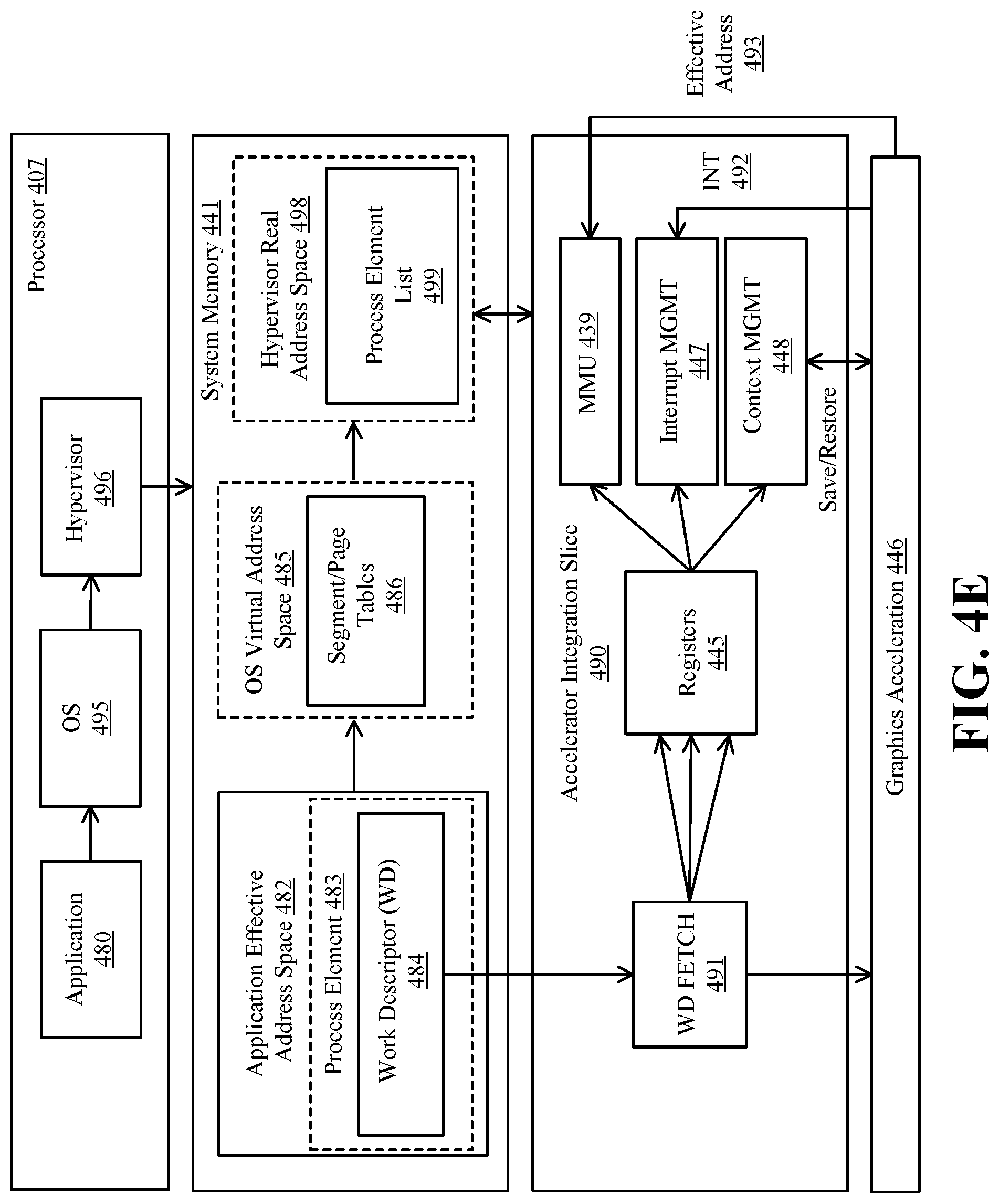
D00013

D00014
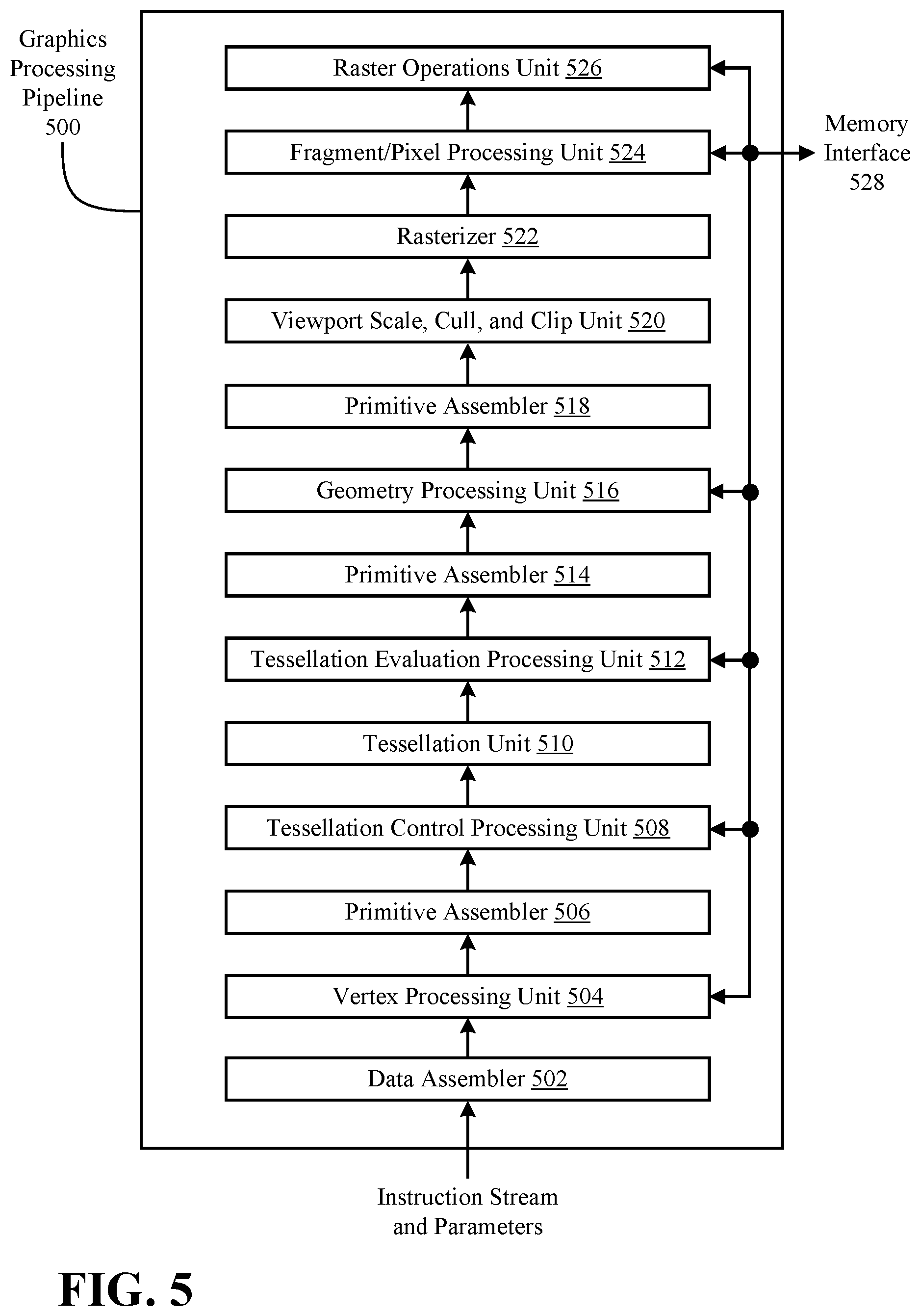
D00015
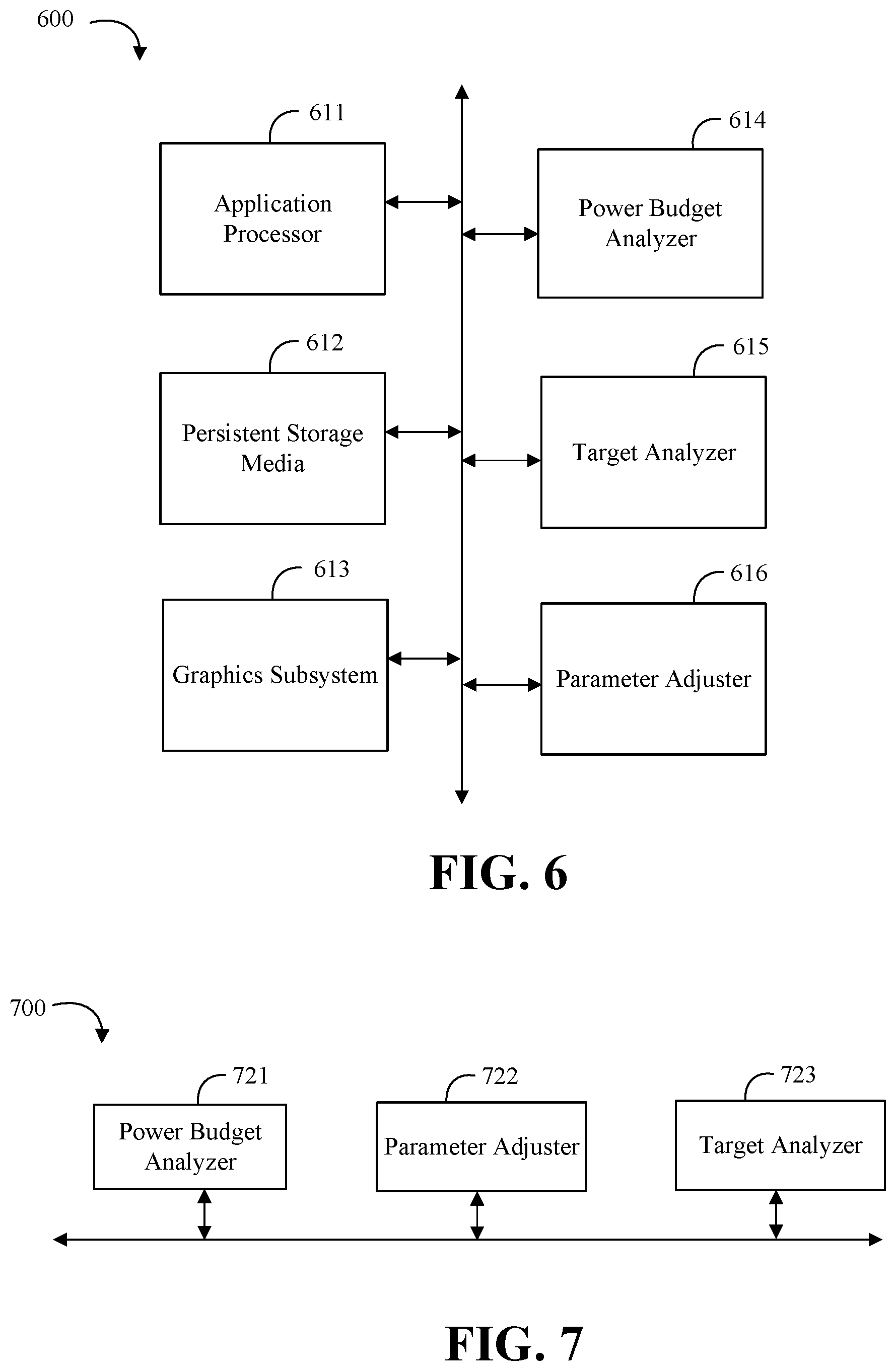
D00016
D00017
D00018
D00019
D00020
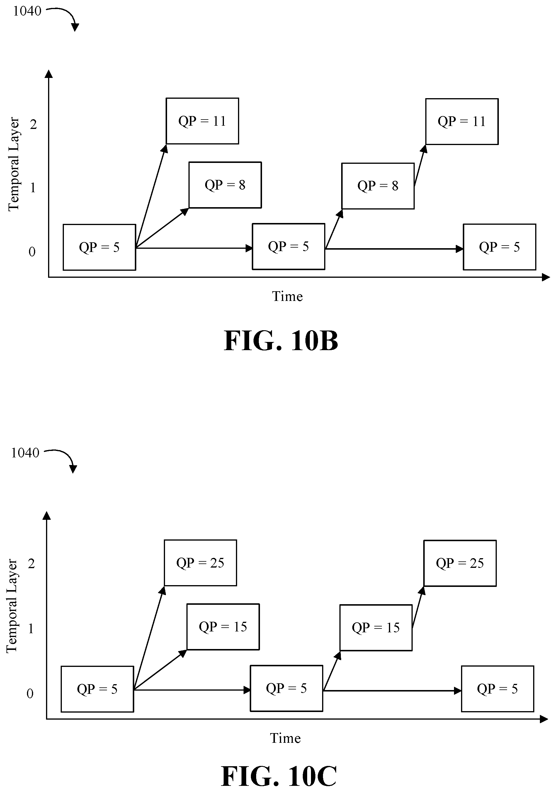
D00021

D00022

D00023
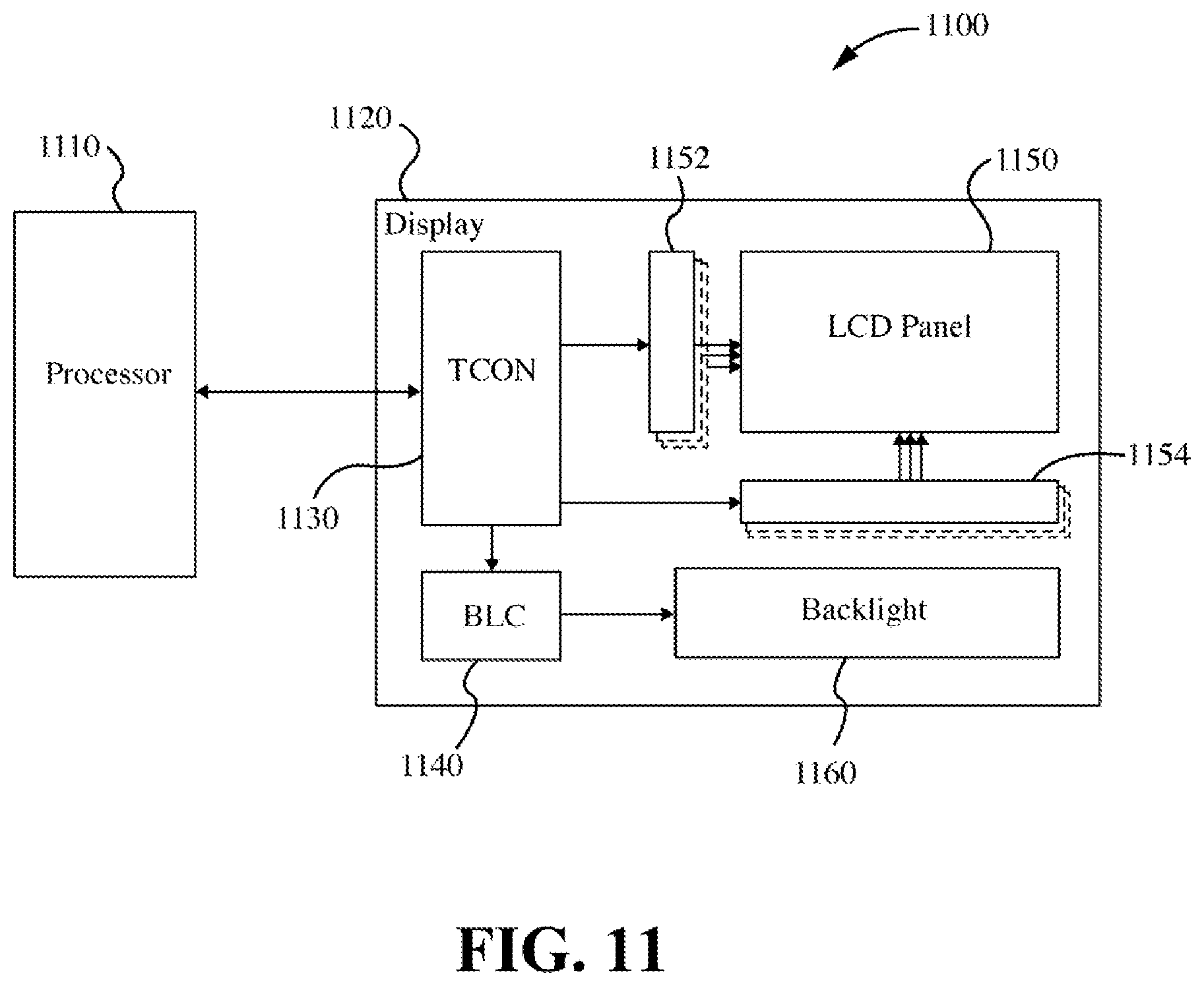
D00024
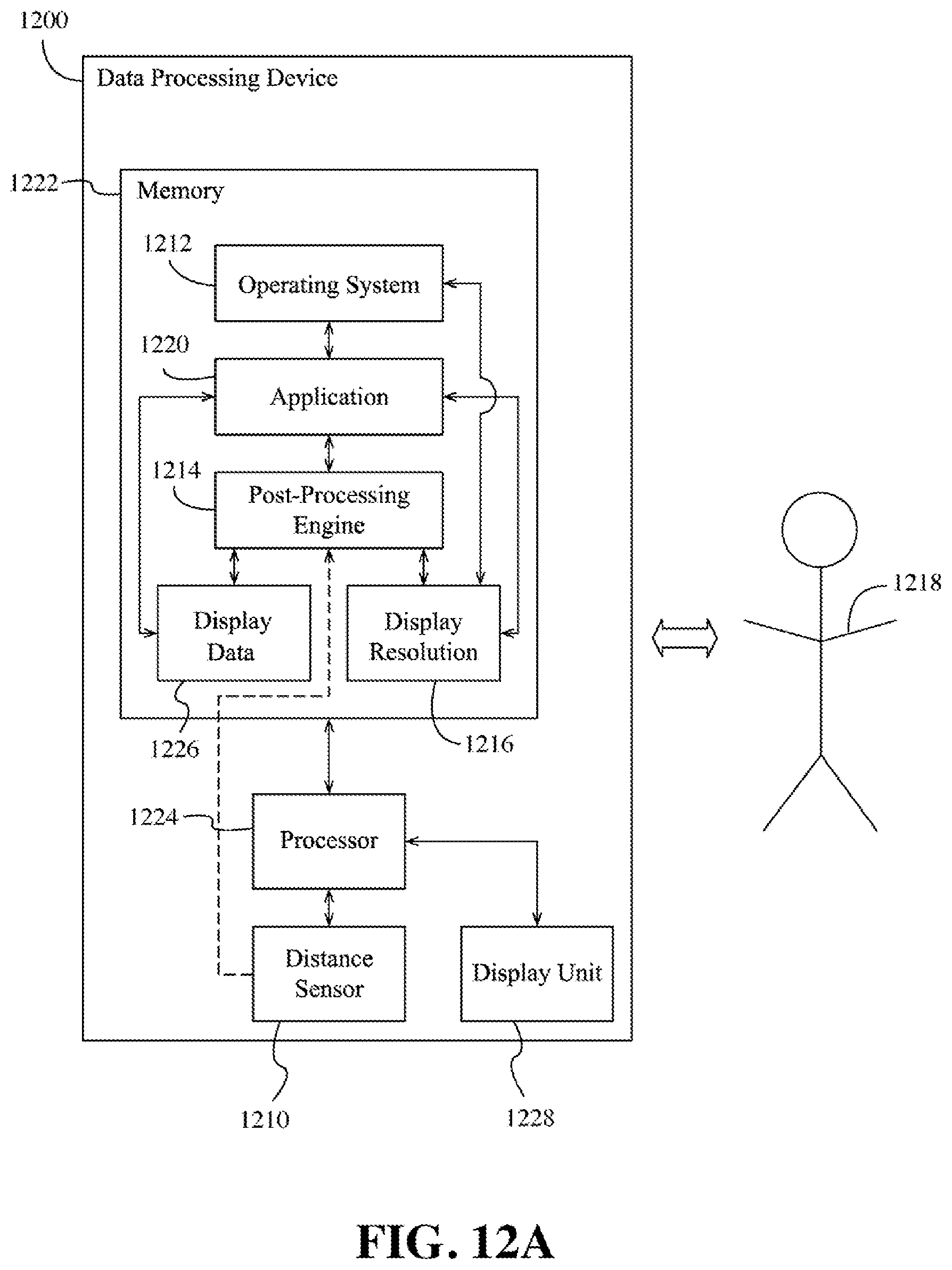
D00025
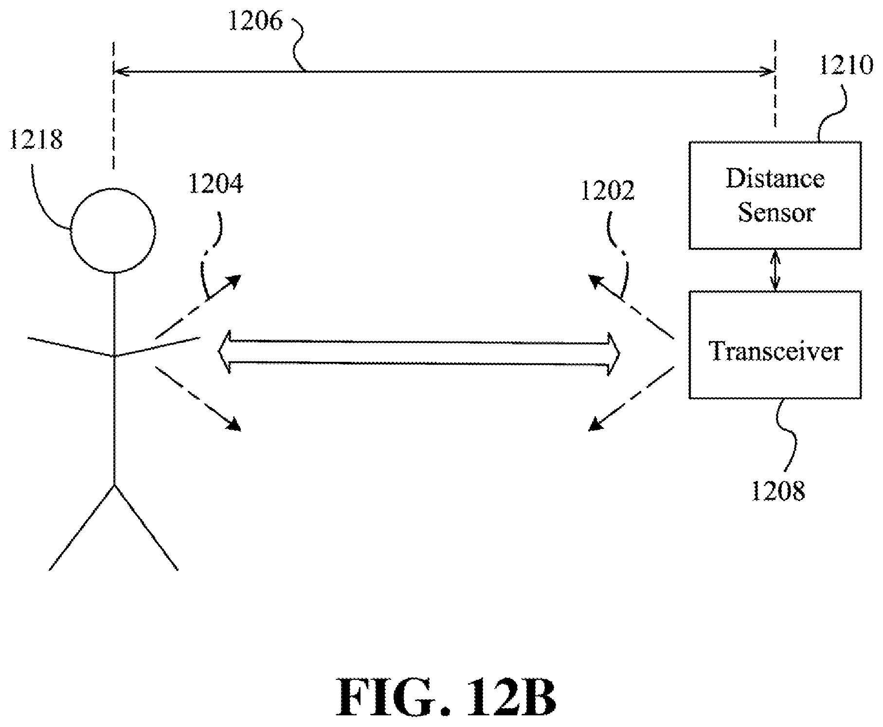
D00026

D00027

D00028
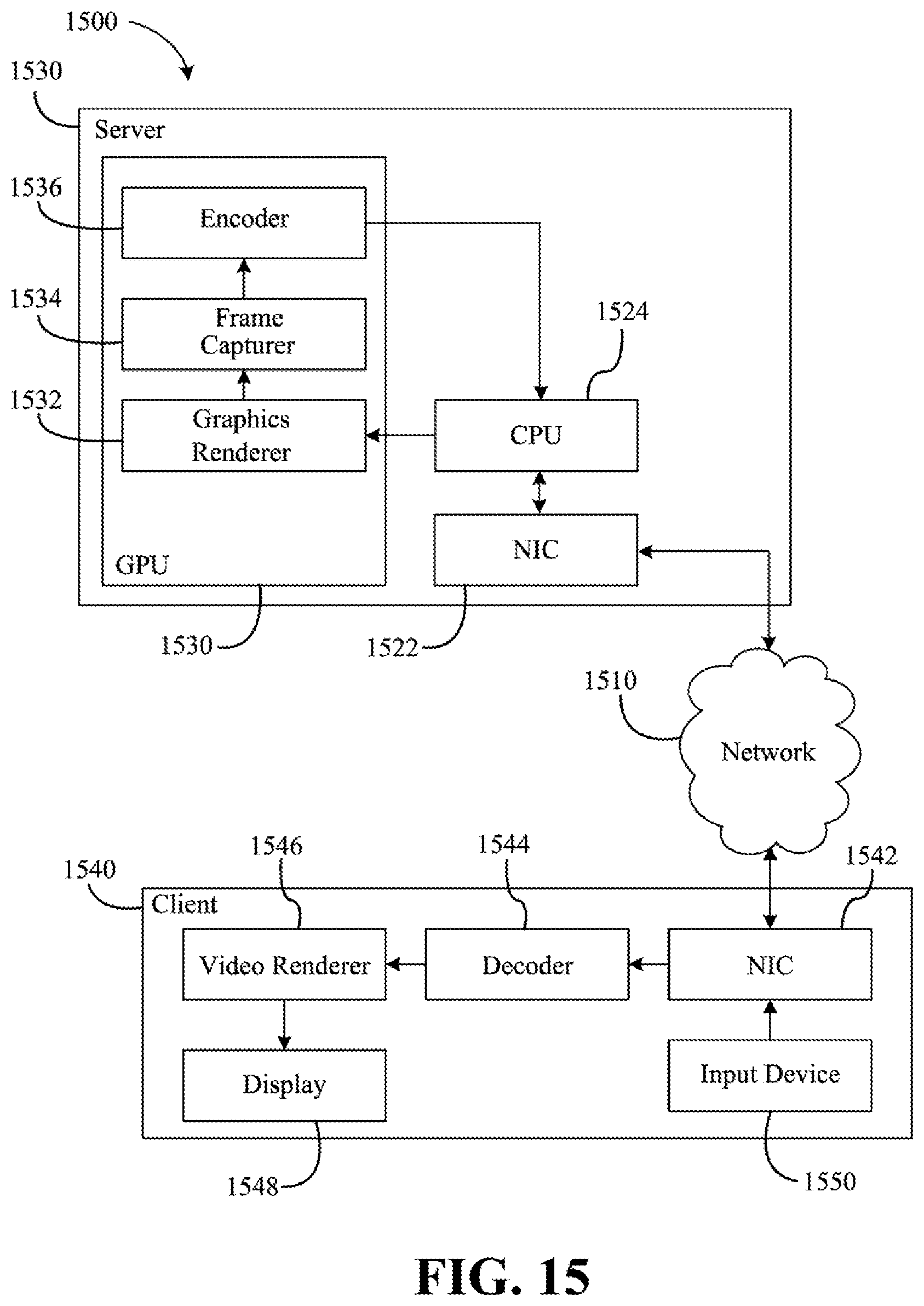
D00029

D00030
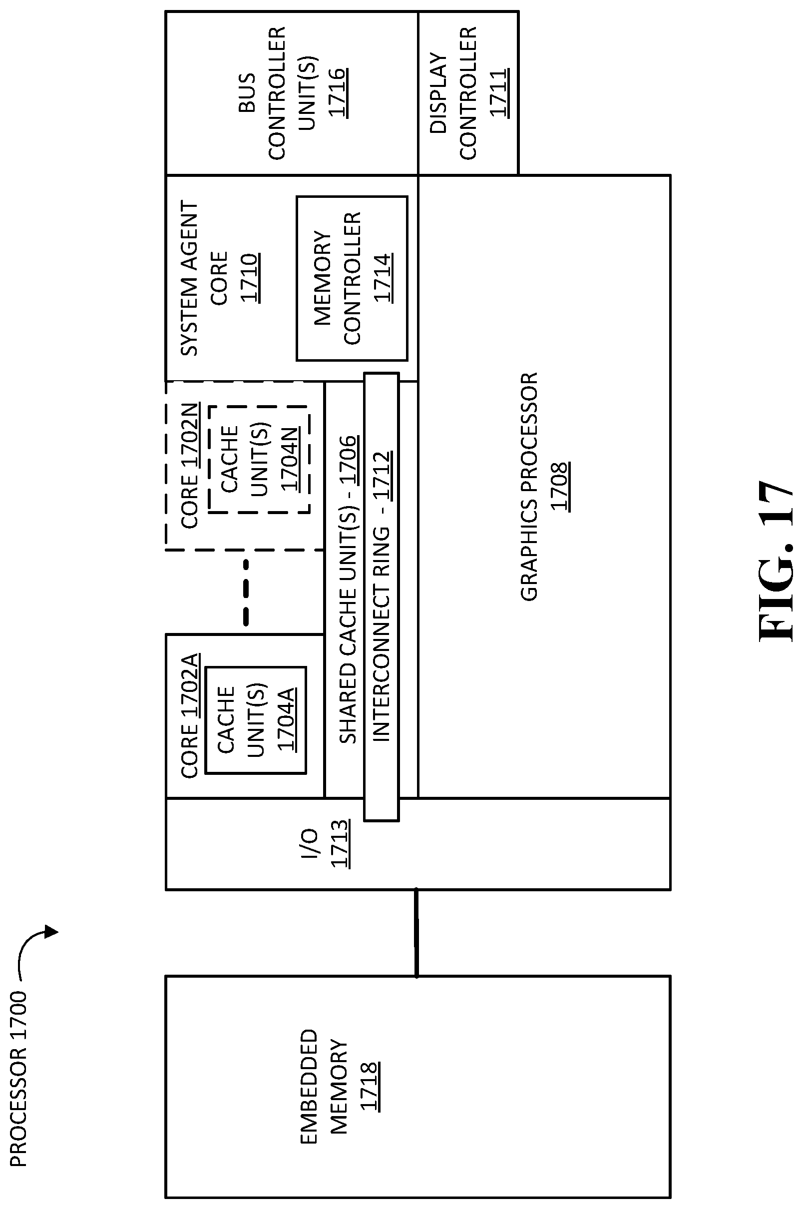
D00031
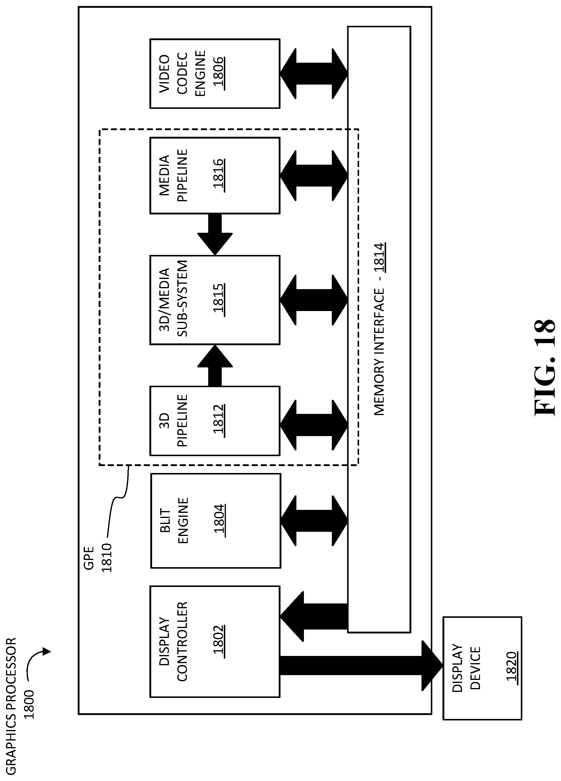
D00032

D00033

D00034

D00035
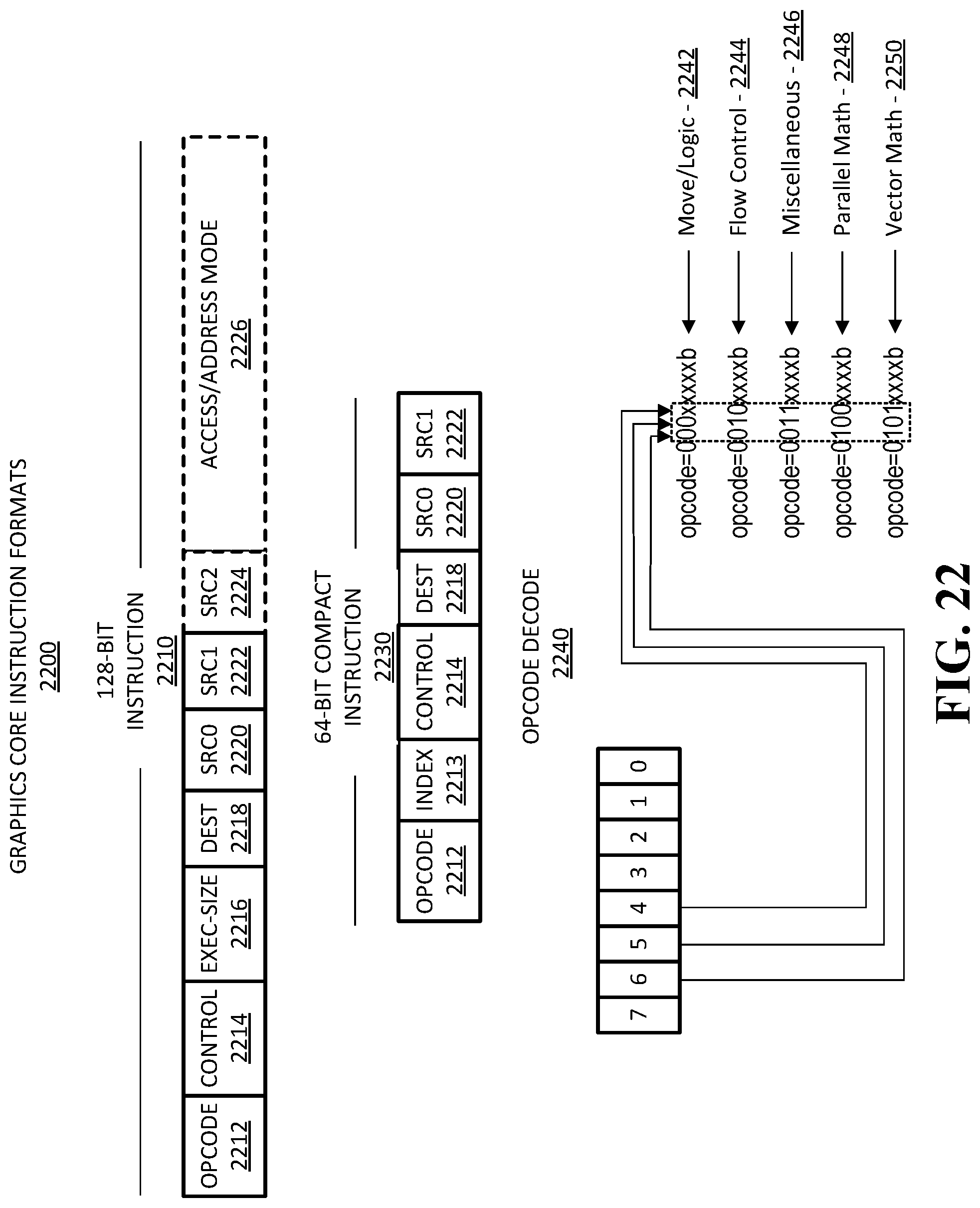
D00036
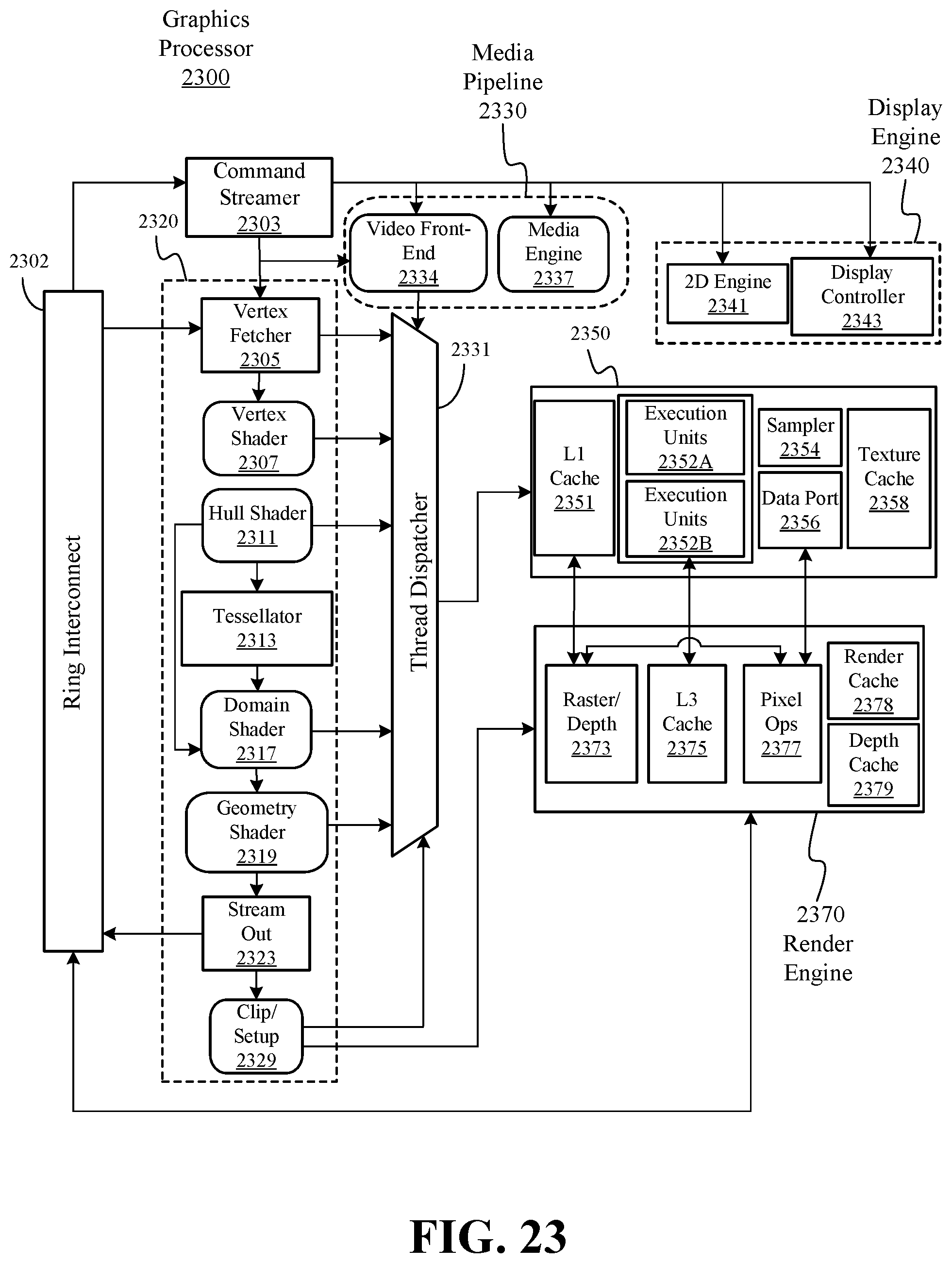
D00037
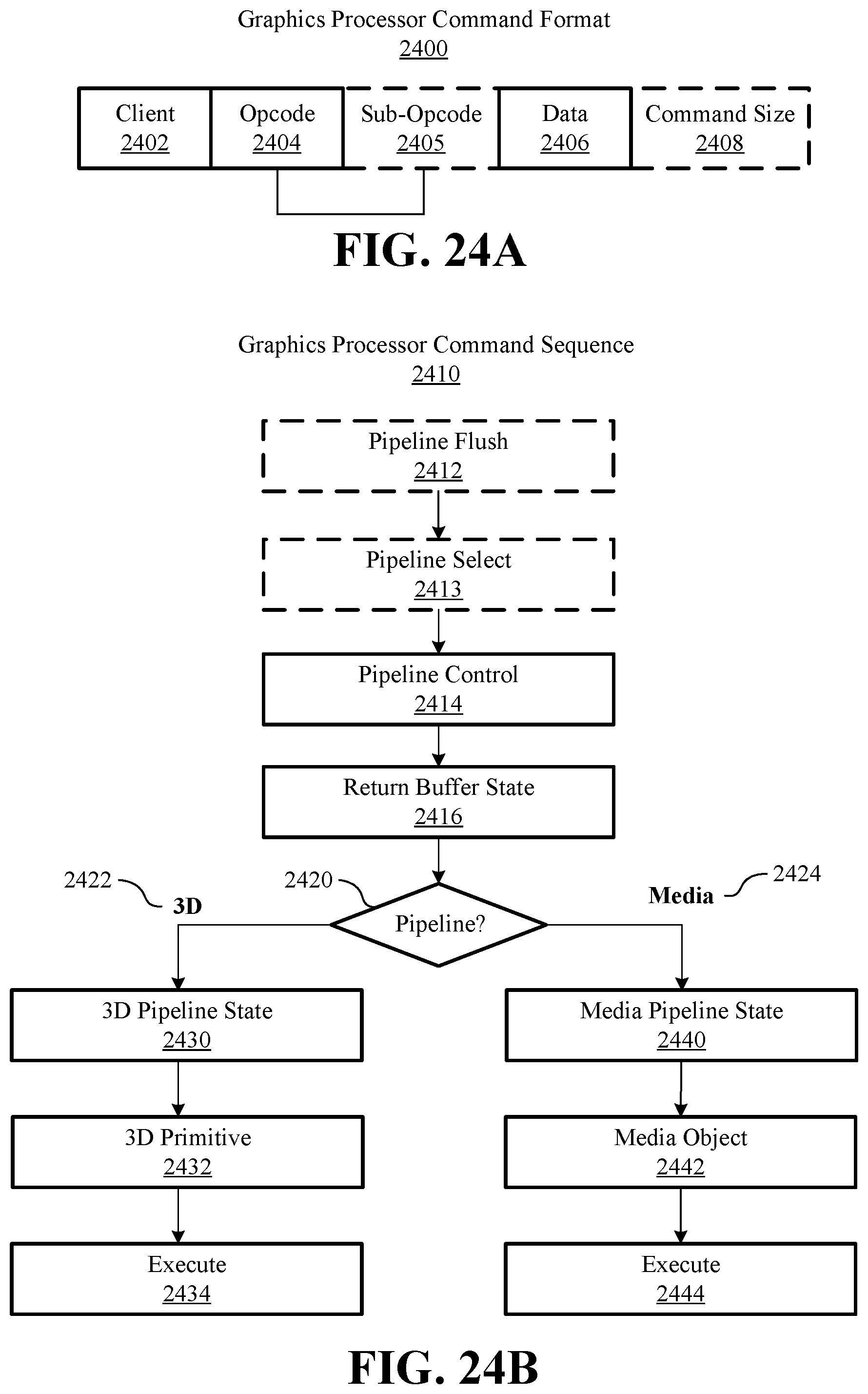
D00038

D00039

D00040

XML
uspto.report is an independent third-party trademark research tool that is not affiliated, endorsed, or sponsored by the United States Patent and Trademark Office (USPTO) or any other governmental organization. The information provided by uspto.report is based on publicly available data at the time of writing and is intended for informational purposes only.
While we strive to provide accurate and up-to-date information, we do not guarantee the accuracy, completeness, reliability, or suitability of the information displayed on this site. The use of this site is at your own risk. Any reliance you place on such information is therefore strictly at your own risk.
All official trademark data, including owner information, should be verified by visiting the official USPTO website at www.uspto.gov. This site is not intended to replace professional legal advice and should not be used as a substitute for consulting with a legal professional who is knowledgeable about trademark law.