Employing optical signals for power and/or communication
Pletcher , et al. December 22, 2
U.S. patent number 10,873,401 [Application Number 16/295,658] was granted by the patent office on 2020-12-22 for employing optical signals for power and/or communication. This patent grant is currently assigned to Verily Life Sciences LLC. The grantee listed for this patent is Verily Life Sciences LLC. Invention is credited to Brian Otis, Nathan Pletcher.


| United States Patent | 10,873,401 |
| Pletcher , et al. | December 22, 2020 |
Employing optical signals for power and/or communication
Abstract
Apparatus, systems and methods employing contact lens sensors are provided. In some aspects, a contact lens includes a substrate that forms at least a portion of the body of the contact lens; an optical communication device disposed on or within the substrate; and a photodetector disposed on or within the substrate, wherein the photodetector harvests light emitted from a device and generates power from the harvested light. In some aspects, an apparatus comprises a tag having a circuit including: an optical communication device; and a photodetector that harvests light received and generates power from the harvested light. The tag can be disposed on or within a contact lens in various aspects.
| Inventors: | Pletcher; Nathan (Mountain View, CA), Otis; Brian (Sunnyvale, CA) | ||||||||||
|---|---|---|---|---|---|---|---|---|---|---|---|
| Applicant: |
|
||||||||||
| Assignee: | Verily Life Sciences LLC
(Mountain View, CA) |
||||||||||
| Family ID: | 1000004039551 | ||||||||||
| Appl. No.: | 16/295,658 | ||||||||||
| Filed: | March 7, 2019 |
Related U.S. Patent Documents
| Application Number | Filing Date | Patent Number | Issue Date | ||
|---|---|---|---|---|---|
| 15645486 | Jul 10, 2017 | 10256919 | |||
| 14850704 | Aug 15, 2017 | 9735892 | |||
| 13559350 | Oct 13, 2015 | 9158133 | |||
| Current U.S. Class: | 1/1 |
| Current CPC Class: | G02C 11/10 (20130101); G02C 7/04 (20130101); A61B 5/72 (20130101); G06K 7/10158 (20130101); A61B 5/01 (20130101); A61B 5/14532 (20130101); A61B 5/0017 (20130101); A61B 5/6821 (20130101); H04B 10/807 (20130101) |
| Current International Class: | G02C 7/04 (20060101); G02C 11/00 (20060101); A61B 5/145 (20060101); A61B 5/00 (20060101); G06K 7/10 (20060101); H04B 10/80 (20130101); A61B 5/01 (20060101) |
| Field of Search: | ;351/159.02,159.03 |
References Cited [Referenced By]
U.S. Patent Documents
| 3958560 | May 1976 | March |
| 4014321 | March 1977 | March |
| 4055378 | October 1977 | Feneberg et al. |
| 4122942 | October 1978 | Wolfson |
| 4136250 | January 1979 | Mueller et al. |
| 4143949 | March 1979 | Chen |
| 4153641 | May 1979 | Deichert et al. |
| 4214014 | July 1980 | Hofer et al. |
| 4309085 | January 1982 | Morrison |
| 4312575 | January 1982 | Peyman et al. |
| 4401371 | August 1983 | Neefe |
| 4463149 | July 1984 | Ellis |
| 4555372 | November 1985 | Kunzler et al. |
| 4604479 | August 1986 | Ellis |
| 4632844 | December 1986 | Yanagihara et al. |
| 4686267 | August 1987 | Ellis et al. |
| 4740533 | April 1988 | Su et al. |
| 4826936 | May 1989 | Ellis |
| 4996275 | February 1991 | Ellis et al. |
| 4997770 | March 1991 | Giles et al. |
| 5032658 | July 1991 | Baron et al. |
| 5034461 | July 1991 | Lai et al. |
| 5070215 | December 1991 | Bambury et al. |
| 5135297 | August 1992 | Valint, Jr. |
| 5177165 | January 1993 | Valint, Jr. et al. |
| 5177168 | January 1993 | Baron et al. |
| 5219965 | June 1993 | Valint, Jr. et al. |
| 5260000 | November 1993 | Nandu et al. |
| 5271875 | December 1993 | Appleton et al. |
| 5310779 | May 1994 | Lai |
| 5321108 | June 1994 | Kunzler et al. |
| 5326584 | July 1994 | Kamel et al. |
| 5336797 | August 1994 | McGee et al. |
| 5346976 | September 1994 | Ellis et al. |
| 5358995 | October 1994 | Lai et al. |
| 5364918 | November 1994 | Valint, Jr. et al. |
| 5387662 | February 1995 | Kunzler et al. |
| 5449729 | September 1995 | Lai |
| 5472436 | December 1995 | Fremstad |
| 5512205 | April 1996 | Lai |
| 5585871 | December 1996 | Linden |
| 5610252 | March 1997 | Bambury et al. |
| 5616757 | April 1997 | Bambury et al. |
| 5682210 | October 1997 | Weirich |
| 5708094 | January 1998 | Lai et al. |
| 5710302 | January 1998 | Kunzler et al. |
| 5714557 | February 1998 | Kunzler et al. |
| 5726733 | March 1998 | Lai et al. |
| 5760100 | June 1998 | Nicolson et al. |
| 5908906 | June 1999 | Kunzler et al. |
| 5981669 | November 1999 | Valint, Jr. et al. |
| 6087941 | July 2000 | Ferraz |
| 6131580 | October 2000 | Ratner et al. |
| 6193369 | February 2001 | Valint, Jr. et al. |
| 6200626 | March 2001 | Grobe, III et al. |
| 6213604 | April 2001 | Valint, Jr. et al. |
| 6312393 | November 2001 | Abreu |
| 6348507 | February 2002 | Heiler et al. |
| 6366794 | April 2002 | Moussy et al. |
| 6423001 | July 2002 | Abreu |
| 6428839 | August 2002 | Kunzler et al. |
| 6431705 | August 2002 | Linden |
| 6440571 | August 2002 | Valint, Jr. et al. |
| 6450642 | September 2002 | Jethmalani et al. |
| 6532298 | March 2003 | Cambier et al. |
| 6550915 | April 2003 | Grobe, III |
| 6570386 | May 2003 | Goldstein |
| 6579235 | June 2003 | Abita et al. |
| 6599559 | July 2003 | McGee et al. |
| 6614408 | September 2003 | Mann |
| 6630243 | October 2003 | Valint, Jr. et al. |
| 6638563 | October 2003 | McGee et al. |
| 6726322 | April 2004 | Andino et al. |
| 6735328 | May 2004 | Helbing et al. |
| 6779888 | August 2004 | Marmo |
| 6804560 | October 2004 | Nisch et al. |
| 6851805 | February 2005 | Blum et al. |
| 6885818 | April 2005 | Goldstein |
| 6939299 | September 2005 | Peterson et al. |
| 6980842 | December 2005 | March et al. |
| 7018040 | March 2006 | Blum et al. |
| 7131945 | November 2006 | Fink et al. |
| 7169106 | January 2007 | Fleischman et al. |
| 7398119 | July 2008 | Lambert et al. |
| 7423801 | September 2008 | Kaufman et al. |
| 7429465 | September 2008 | Muller et al. |
| 7441892 | October 2008 | Hsu |
| 7443016 | October 2008 | Tsai et al. |
| 7450981 | November 2008 | Jeon |
| 7639845 | December 2009 | Utsunomiya |
| 7654671 | February 2010 | Glynn |
| 7699465 | April 2010 | Dootjes et al. |
| 7728949 | June 2010 | Clarke et al. |
| 7751896 | July 2010 | Graf et al. |
| 7799243 | September 2010 | Mather et al. |
| 7809417 | October 2010 | Abreu |
| 7878650 | February 2011 | Fritsch et al. |
| 7885698 | February 2011 | Feldman |
| 7907931 | March 2011 | Hartigan et al. |
| 7926940 | April 2011 | Blum et al. |
| 7931832 | April 2011 | Pugh et al. |
| 7964390 | June 2011 | Rozakis et al. |
| 8080187 | December 2011 | Tepedino, Jr. et al. |
| 8096654 | January 2012 | Amirparviz et al. |
| 8118752 | February 2012 | Hetling et al. |
| 8142016 | March 2012 | Legerton et al. |
| 8224415 | July 2012 | Budiman |
| 8446341 | May 2013 | Amirparviz |
| 8827445 | September 2014 | Wiser et al. |
| 9158133 | October 2015 | Pletcher |
| 9735892 | August 2017 | Pletcher et al. |
| 10256919 | April 2019 | Pletcher et al. |
| 2002/0193674 | December 2002 | Fleischman et al. |
| 2003/0179094 | September 2003 | Abreu |
| 2004/0027536 | February 2004 | Blum et al. |
| 2004/0116794 | June 2004 | Fink et al. |
| 2005/0045589 | March 2005 | Rastogi et al. |
| 2005/0221276 | October 2005 | Rozakis et al. |
| 2007/0016074 | January 2007 | Abreu |
| 2007/0030443 | February 2007 | Chapoy et al. |
| 2007/0121065 | May 2007 | Cox et al. |
| 2007/0188710 | August 2007 | Hetling et al. |
| 2008/0208335 | August 2008 | Blum et al. |
| 2008/0218696 | September 2008 | Mir |
| 2009/0033863 | February 2009 | Blum et al. |
| 2009/0036761 | February 2009 | Abreu |
| 2009/0057164 | March 2009 | Minick et al. |
| 2009/0076367 | March 2009 | Sit et al. |
| 2009/0118604 | May 2009 | Phan et al. |
| 2009/0189830 | July 2009 | Deering et al. |
| 2009/0196460 | August 2009 | Jakobs et al. |
| 2010/0001926 | January 2010 | Amirparviz et al. |
| 2010/0013114 | January 2010 | Bowers et al. |
| 2010/0016704 | January 2010 | Naber et al. |
| 2010/0028559 | February 2010 | Yan et al. |
| 2010/0072643 | March 2010 | Pugh et al. |
| 2010/0109175 | May 2010 | Pugh et al. |
| 2010/0110372 | May 2010 | Pugh et al. |
| 2010/0113901 | May 2010 | Zhang et al. |
| 2010/0133510 | June 2010 | Kim et al. |
| 2010/0249548 | September 2010 | Muller |
| 2011/0015512 | January 2011 | Pan et al. |
| 2011/0028807 | February 2011 | Abreu |
| 2011/0040161 | February 2011 | Abreu |
| 2011/0055317 | March 2011 | Vonog et al. |
| 2011/0063556 | March 2011 | Ahn |
| 2011/0084834 | April 2011 | Sabeta |
| 2011/0116035 | May 2011 | Fritsch et al. |
| 2011/0157541 | June 2011 | Peyman |
| 2011/0157544 | June 2011 | Pugh et al. |
| 2011/0184271 | July 2011 | Veciana et al. |
| 2011/0274680 | November 2011 | Mazed et al. |
| 2011/0286064 | November 2011 | Burles et al. |
| 2011/0298794 | December 2011 | Freedman |
| 2012/0026458 | February 2012 | Qiu et al. |
| 2012/0038881 | February 2012 | Amirparviz et al. |
| 2012/0041287 | February 2012 | Goodall et al. |
| 2012/0041552 | February 2012 | Chuck et al. |
| 2012/0069254 | March 2012 | Burton |
| 2012/0075168 | March 2012 | Osterhout et al. |
| 2012/0075574 | March 2012 | Pugh et al. |
| 2012/0078071 | March 2012 | Bohm et al. |
| 2012/0088258 | April 2012 | Bishop et al. |
| 2012/0092612 | April 2012 | Binder |
| 2012/0109296 | May 2012 | Fan |
| 2012/0177576 | July 2012 | Hu |
| 2012/0201755 | August 2012 | Rozakis et al. |
| 2012/0245444 | September 2012 | Otis et al. |
| 2012/0259188 | October 2012 | Besling |
| 0369942 | May 1990 | EP | |||
| 686372 | Dec 1995 | EP | |||
| 1061874 | Dec 2000 | EP | |||
| 1617757 | Jan 2006 | EP | |||
| 1818008 | Aug 2007 | EP | |||
| 1947501 | Jul 2008 | EP | |||
| 2457122 | May 2012 | EP | |||
| 9504609 | Feb 1995 | WO | |||
| 0116641 | Mar 2001 | WO | |||
| 0134312 | May 2001 | WO | |||
| 03065876 | Aug 2003 | WO | |||
| 2004060431 | Jul 2004 | WO | |||
| 2004064629 | Aug 2004 | WO | |||
| 2006015315 | Feb 2006 | WO | |||
| 2009094643 | Jul 2009 | WO | |||
| 2010105728 | Sep 2010 | WO | |||
| 2010133317 | Nov 2010 | WO | |||
| 2011011344 | Jan 2011 | WO | |||
| 2011034592 | Mar 2011 | WO | |||
| 2011035228 | Mar 2011 | WO | |||
| 2011035262 | Mar 2011 | WO | |||
| 2011083105 | Jul 2011 | WO | |||
| 2011163080 | Dec 2011 | WO | |||
| 2012035429 | Mar 2012 | WO | |||
| 2012037455 | Mar 2012 | WO | |||
| 2012051167 | Apr 2012 | WO | |||
| 2012051223 | Apr 2012 | WO | |||
| 2012052765 | Apr 2012 | WO | |||
Other References
|
Badugu et al., "A Glucose Sensing Contact Lens: A Mon-Invasive Technique for Continuous Physiological Glucose Monitoring", Journal of Fluorescence, Sep. 2003, pp. 371-374, vol. 13, No. 5. cited by applicant . Carlson et al., "A 20 mV Input Boost Converter With Efficient Digital Control for Thermoelectric Energy Harvesting," IEEE Journal of Solid-State Circuits, Apr. 2010, pp. 741-750, vol. 45, No. 4. cited by applicant . Chu et al., "Biomedical soft contact-lens sensor for in situ ocular biomonitoring of tear contents," Biomed Microdevices, 2011, pp. 603-611, vol. 13. cited by applicant . Chu et al., "Soft contact lens biosensor for in situ monitoring of tear glucose as non-invasive blood sugar assessment," Talanta, 2011, pp. 960-965, vol. 83. cited by applicant . "Contact Lenses: Look Into My Eyes," The Economist, Jun. 2, 2011 , http:/ /www.economist.com/node/ 187 50624/ print, Last accessed Mar. 13, 2012, 8 pages. cited by applicant . Haders, "New Controlled Release Technologies Broaden Opportunities for Ophthalmic Therapies," Drug Delivery Technology, Jul./Aug. 2009, pp. 48-53, vol. 8, No. 7. cited by applicant . Ho et al., "Contact Lens With Integrated Inorganic Semiconductor Devices," MEMS 2008. IEEE 21st International Conference on. IEEE, 2008., pp. 403-406. cited by applicant . Holloway, "Microsoft developing electronic contact lens to monitor blood sugar," Gizmag, Jan. 5, 2012, http://www.gizmag.com/microsoft-electronic-diabetic-contact-lens/20987 /, Last accessed Mar. 13, 2012, 5 pages. cited by applicant . Landesmaki et al., "Possibilities for Continuous Glucose Monitoring by a Functional Contact Lens," IEEE Instrumentation & Measurement Magazine, Jun. 2010, pp. 14-17. cited by applicant . Lingley et al., "A contact lens with integrated micro solar cells," Microsyst Techno!, 2012, pp. 453-458, vol. 18. cited by applicant . Murdan, "Electro-responsive drug delivery from hydro gels," Journal of Controlled Release, 2003, pp. 1-17, vol. 92. cited by applicant . Parviz, Babak A., "For Your Eyes Only," IEEE Spectrum, Sep. 2009, pp. 36-41. cited by applicant . Saeedi, E. et al., "Self-assembled crystalline semiconductor optoelectronics on glass and plastic," J. Micromech. Microeng., 2008, pp. 1-7, vol. 18. cited by applicant . Saeedi et al., "Self-Assembled Inorganic Micro-Display on Plastic," Micro Electro Mechanical Systems, 2007. MEMS. IEEE 20th International Conference on. IEEE, 2007, pp. 755-758. cited by applicant . Sensimed Triggerfish, Sensimed Brochure, 2010, 10 pages. cited by applicant . Shin, Yi-Chun et al., "An Inductorless DC-DC Converter for Energy Harvesting With a 1.2! W Bandgap-Referenced Output Controller," IEEE Transactions on Circuits and Systems-II: Express Briefs, Dec. 2011, pp. 832-836, vol. 58, No. 12. cited by applicant . Shum et al., "Functional modular contact lens," Proc. of SPIE, 2009, pp. 73970K-I to 73970K-8, vol. 7397. cited by applicant . Singh, et al., "Novel Approaches in Formulation and Drug Delivery using Contact Lenses," Journal of Basic and Clinical Pharmacy, May 2011, pp. 87-101, vol. 2, Issue 2. cited by applicant . Stauth et al., "Self-assembled single-crystal silicon circuits on plastic," PNAS, Sep. 19, 2006, pp. 13922-13927, vol. 103, No. 38. cited by applicant . Yao, H. et al. "A contact lens with integrated telecommunication circuit and sensors for wireless and continuous tear ilucose monitoring," J. Micromech. Microeng., 2012, pp. 1-10, vol. 22. cited by applicant . Yao, H. et al., "A Dual Microscal Glucose Sensor on a Contact Lens, Tested in Conditions Mimicking the Eye," Micro Electro Mechanical Systems (MEMS), 2011 IEEE 24th International Conference on. IEEE, 2011, pp. 25-28. cited by applicant . Yao et al., "A contact lens with embedded sensor for monitoring tear glucose level," Biosensors and Bioelectronics, 2011, pp. 3290-3296, vol. 26. cited by applicant . Yao, H. et al., "A Soft Hydrogel Contact Lens with an Encapsulated Sensor for Tear Glucose Monitoring," Micro Electro Mechanical Systems (MEMS), 2012 IEEE 25th International Conference on. IEEE, 2012, pp. 769-772. cited by applicant . Yeager et al., "A 9 uA, Addressable Gent Sensor Tag for Biosignal Acquistion," IEEE Journal of Solid-State Circuits, Oct. 2010, pp. 2198-2209, vol. 45, No. 10. cited by applicant . Zhang et al., "Design for Ultra-Low Power Biopotential Amplifiers for Biosignal Acquistion Applications," IEEE Transactions on Biomedical Circuits and Systems, 2012, pp. 344-355, vol. 6, No. 4. cited by applicant . Wall, K., "Active contact lens that lets you see like the Terminator patented," Feb. 10, 2012, http://www.patexia.com/feed/active-contactlens-that-lets-you-see-like-the- -terminator-patented-2407, Last accessed Mar. 28, 2012, 5 pages. cited by applicant . Parviz, Babak A., "Augmented Reality in a Contact Lens," IEEE Spectrum, Sep. 2009, http://spectrumieee.org/biomedical/bionics/augmented-reality-in-a-contact- -lens/0, Last accessed Mar. 14, 2012, 6 pages. cited by applicant . Bionic contact lens `To project emails before eyes,` http://www.kurzweilai.net/forums/topic/bionic-contact-lens-to-project-ema- ilsbefore-eyes, Last accessed Mar. 14, 2012, 2 pages. cited by applicant . Tweedie, et al., "Contact creep compliance of viscoelastic materials via nanoindentation," J. Mater. Res., Jun. 2006, vol. 21, No. 2, pp. 157 6-15 89, Materials Research Society. cited by applicant . Brahim, et al., "Polypyrrole-hydrogel composites for the construction of clinically important biosensors," 2002, Biosensors & Bioelectronics, vol. 17, pp. 53-59. cited by applicant . Huang, et al., "Wrinkling of Ultrathin Polymer Films," Mater. Res. Soc. Symp. Proc., 2006, vol. 924, 6 pages, Materials Research Society. cited by applicant . Zarbin, et al., "Nanotechnology in ophthalmology," Can J Ophthahnol, 2010, vol. 45, No. 5, pp. 457-476. cited by applicant . Selner, et al., "Novel Contact Lens Electrode Array for Multielectrode Electroretinography (meERG)," IEEE, 2011, 2 pages. cited by applicant . Liao, et al., "A 3-uW CMOS Glucose Sensor for Wireless Contact Lens Tear Glucose Monitoring," IEEE Journal of Solid-State Circuits, Jan. 2012, vol. 47, No. 1, pp. 335-344. cited by applicant . Chen, et al., "Microfabricated Implantable Parylene-Based Wireless Passive Intraocular Pressure Sensors," Journal of Microelectromechanical Systems, Dec. 2008, vol. 17, No. 6, pp. 1342-1351. cited by applicant . Thomas, et al., "Functional Contact Lenses for Remote Health Monitoring in Developing Countries," IEEE Global Humanitarian Technology Conference, 2011, pp. 212-217, IEEE Computer Society. cited by applicant . Pandey, et al., "A Fully Integrated RF-Powered Contact Lens With a Single Element Display," IEEE Transactions on Biomedical Circuits and Systems, Dec. 2010, vol. 4, No. 6, pages. cited by applicant . Lingley, et al., "Multipurpose integrated active contact lenses," SPIE, 2009, 2 pages. cited by applicant . Chu, et al., "Soft Contact-lens Sensor for Monitoring Tear Sugar as Novel Wearable Device of Body Sensor Network," http://www.ksi.edu/seke/dms11/DMS/2_Kohji_Mitsubayashi.pdf, Last accessed Jul. 27, 2012, 4 pages. cited by applicant . Liao, et al., "A 3uW Wirelessly Powered CMOS Glucose Sensor for an Active Contact Lens," 2011 IEEE International Solid-State Circuits Conference, Session 2, Feb. 21, 2011, 3 pages. cited by applicant . Hurst, "How contact lenses could help save your life," Mail Online, Apr. 19, 2010, http://www.dailymail.co.uk/health/article-1267345/How-contact-l- enses-help-save-life.htrnl, Last accessed Jul. 27, 2012. cited by applicant . Loncar, et al., "Design and Fabrication of Silicon Photonic Crystal Optical Waveguides," Journal of Lightwave Technology, Oct. 2000, vol. 18, No. 10, pp. 1402-1411. cited by applicant . Baxter, "Capacitive Sensors," 2000, 17 pages. cited by applicant . Lingley, et al., "A Single-Pixel Wireless Contact Lens Display," Journal of Micromechanics and Microengineering, 2011, 9 pages. cited by applicant. |
Primary Examiner: Dang; Hung X
Attorney, Agent or Firm: McDonnell Boehnen Hulbert & Berghoff LLP
Parent Case Text
CROSS-REFERENCE TO RELATED APPLICATIONS
This application is a continuation if application Ser. No. 15/645,486, filed Jul. 10, 2017, now U.S. Pat. No. 10,256,919, which is a continuation of application Ser. No. 14/850,704, filed Sep. 10, 2015, now U.S. Pat. No. 9,735,892 which is a continuation of application Ser. No. 13/559,350, filed Jul. 26, 2012 now U.S. Pat. No. 9,158,133. The foregoing applications are incorporated herein by reference.
Claims
What is claimed is:
1. A sensing device, comprising: one or more sensors configured to sense one or more biological features associated with an eye; a photodetector, wherein the photodetector is configured to harvest ambient light and to generate power from the harvested light; and an optical communication device configured to transmit an optical signal, wherein the optical signal communicates information about the one or more sensed biological features.
2. The sensing device of claim 1, wherein the photodetector comprises at least one of a photovoltaic cell or a solar cell.
3. The sensing device of claim 1, wherein the optical communication device comprises a light-emitting diode (LED).
4. The sensing device of claim 1, wherein the optical communication device comprises a reflector.
5. The sensing device of claim 1, wherein the one or more sensors are powered by the power generated from the harvested light.
6. The sensing device of claim 1, wherein the optical communication device is powered by the power generated from the harvested light.
7. The sensing device of claim 1, wherein the optical communication device is configured to modulate the optical signal with the information about the one or more sensed biological features.
8. The sensing device of claim 1, wherein the optical signal comprises visible light.
9. The sensing device of claim 1, wherein the optical signal comprises infrared light.
10. The sensing device of claim 1, further comprising a transparent substrate that forms at least part of a body of the sensing device.
11. The sensing device of claim 10, wherein the photodetector is disposed on or within the transparent substrate.
12. The sensing device of claim 10, wherein the one or more sensors are disposed on or within the transparent substrate.
13. The sensing device of claim 10, wherein the optical communication device is disposed on or within the transparent substrate.
14. The sensing device of claim 1, further comprising a microprocessor.
15. The sensing device of claim 1, further comprising a memory.
16. A method, comprising: sensing, by one or more sensors in a sensing device at an eye, one or more biological features associated with the eye; harvesting, by a photodetector in the sensing device, ambient light to generate power for the sensing device; and transmitting, by an optical communication device in the sensing device, an optical signal, wherein the optical signal communicates information about the one or more sensed biological features.
17. The method of claim 16, further comprising: powering the one or more sensors by the power generated from the harvested light.
18. The method of claim 16, further comprising: powering the optical communication device by the power generated from the harvested light.
19. The method of claim 16, further comprising: modulating, by the optical communication device, the optical signal with the information about the one or more sensed biological features.
20. The method of claim 16, wherein the sensing device comprises a memory, further comprising: storing the information about the one or more sensed biological features in the memory.
Description
TECHNICAL FIELD AND SUMMARY
This disclosure generally relates to a contact lens employing optical signals for power and/or communication. In one aspect, a sensing device comprises: one or more sensors configured to sense one or more biological features associated with an eye; a photodetector, wherein the photodetector is configured to harvest ambient light and to generate power from the harvested light; and an optical communication device configured to transmit an optical signal, wherein the optical signal communicates information about the one or more sensed biological features. In another aspect, a method comprises: sensing, by one or more sensors in a sensing device at an eye, one or more biological features associated with the eye; harvesting, by a photodetector in the sensing device, ambient light to generate power for the sensing device; and transmitting, by an optical communication device in the sensing device, an optical signal, wherein the optical signal communicates information about the one or more sensed biological features.
DESCRIPTION OF THE DRAWINGS
FIGS. 1, 2 and 3 are illustrations of diagrams of exemplary non-limiting systems that facilitate contact lenses employing optical signals for power and/or communication in accordance with aspects described herein.
FIG. 4 is an illustration of a block diagram of a tag for a contact lens facilitating optical communication in accordance with aspects described herein.
FIGS. 5, 6 and 7 are exemplary flow diagrams of methods that facilitate contact lenses employing optical signals for power and/or communication in accordance with aspects described herein.
FIG. 8 is an illustration of a schematic diagram of an exemplary networked or distributed computing environment with which one or more aspects described herein can be associated.
FIG. 9 is an illustration of a schematic diagram of an exemplary computing environment with which one or more aspects described herein can be associated.
DETAILED DESCRIPTION
Various aspects are now described with reference to the drawings, wherein like reference numerals are used to refer to like elements throughout. In the following description, for purposes of explanation, numerous specific details are set forth in order to provide a more thorough understanding of one or more aspects. It is be evident, however, that such aspects can be practiced without these specific details. In other instances, structures and devices are shown in block diagram form in order to facilitate describing one or more aspects.
As used in this application, the terms "component," "component," "system," and the like are intended to refer to a computer-related entity, either hardware, software, firmware, a combination of hardware and software, software and/or software in execution. For example, a component can be, but is not limited to being, a process running on a processor, a processor, an object, an executable, a thread of execution, a program, and/or a computer. By way of illustration, both an application running on a computing device and/or the computing device can be a component. One or more components can reside within a process and/or thread of execution and a component can be localized on one computer and/or distributed between two or more computers. In addition, these components can execute from various computer-readable storage media having various data structures stored thereon. The components can communicate by way of local and/or remote processes such as in accordance with a signal having one or more data packets (e.g., data from one component interacting with another component in a local system, distributed system, and/or across a network such as the Internet with other systems by way of the signal).
The word "exemplary" is used herein to mean serving as an example, instance, or illustration. For the avoidance of doubt, the subject matter disclosed herein is not limited by such examples. In addition, any aspect or design described in this disclosure as "exemplary" is not necessarily to be construed as preferred or advantageous over other aspects or designs, nor is it meant to preclude equivalent exemplary structures and techniques known to those of ordinary skill in the art. Furthermore, to the extent that the terms "includes," "has," "contains," and other similar words are used in either the detailed description or the claims, for the avoidance of doubt, such terms are intended to be inclusive in a manner similar to the term "comprising" as an open transition word without precluding any additional or other elements.
It is to be appreciated that in accordance with one or more aspects described in this disclosure, users can opt-in or opt-out of providing personal information, demographic information, location information, proprietary information, sensitive information, or the like in connection with data gathering aspects. Moreover, one or more aspects described herein can provide for anonymizing collected, received, or transmitted data.
Active contact lens systems generally do not include an on-board energy source due to space and power limitations on the contact lens. Accordingly, RF harvesting and corresponding backscatter can be used for powering the contact lens and, in some cases, communicating with the contact lens. However, specialized and dedicated RF electronics would typically be required to facilitate RF power and communication; and such electronics can be complex and expensive.
Optical communication is a form of telecommunication that employs light as a transmission medium. Optical signals can be advantageous for enabling power generation and/or communication on a small-scale, such as those areas typically required for active contact lenses. A light transmitter can emit a light signal, which can be received by a light detector.
Micro-fabrication techniques can be employed to provide components that can receive and/or transmit light from or to the contact lens. For example, optical waveguides can be designed and fabricated that incorporate two-dimensional (2-D) photonic crystal geometry for lateral confinement of light, and total internal reflection for vertical confinement. Square, triangular or other suitable photonic crystal lattices can be utilized. In an aspect, a three-dimensional (3-D) finite-difference time-domain (FDTD) can be used to find design parameters of the photonic crystal and to calculate dispersion relations for guided modes in a waveguide structure. In an aspect, the waveguides can be fabricated so as to improve confinement in a particular direction and symmetry properties of the structure. High-resolution fabrication can provide for different types of bends and optical cavities within the waveguides. The optical waveguides can facilitate directing light to and from components of the contact lens, and facilitate mitigation of losses associated with dispersion of light.
Sensors can be employed on the contact lens to facilitate power generation from light. Photodetectors are one such type of sensor that can facilitate power generation. Photodetectors are typically made of a photodiode and circuitry that outputs a current in response to detected light. These types of detectors can harvest light emitted from the light source and generate power from the harvested light.
Optical communication devices (e.g., reflectors, light-emitting diodes (LEDs)) that utilize light can be employed to communicate in response to light received. Communication can be performed by modulation of optical data back to a receiver. For example, a modulating retro-reflector (MRR) system can modulate received light (thereby changing the intensity of the light) and reflect the received light back to a light source. Any number of well-known optical modulation techniques can be employed. Additionally, the small-scale of the MRR system can facilitate on-board power savings up to an order of magnitude over the power consumption of typical RF systems.
Multiple optical transmitters can be situated on the contact lens and multiplex and/or modulate multiple optical signals (e.g., using different sources as well as different colors, or wavelength frequencies) in order to enhance encoding of data (e.g., data sensed on the contact lens). For example, optical signals can be modulated with data whereby the modulation type is a function of the data being transmitted.
Further, an optical add-drop multiplexing device can multiplex different sources of light for transmission from the contact lens. In this case, more than one modulated light signal is transmitted on the same carrier, or channel. Different channels can be encoded with the same or different data, and multiplexed prior to transmission.
Apparatus, systems and methods disclosed herein relate to contact lenses employing optical signals for power and/or communication. In one or more aspects, a contact lens can include: a substrate that forms at least a portion of the body of the contact lens; an optical communication device disposed on or within the substrate; and a photodetector disposed on or within the substrate, wherein the photodetector harvests light emitted from a device and generates power from the harvested light, wherein the device is located external to the contact lens.
In one or more aspects, the disclosed subject matter relates to a system. The system can include: a contact lens and a device. The contact lens can include: a substrate; and a circuit disposed on or within the substrate. The circuit can include: one or more sensors that sense a feature of a wearer of the contact lens; a communication component that outputs information indicative of the sensed feature from the contact lens; a processor that processes the information indicative of the sensed feature; and one or more light sensors that sense light and power at least one of the component or the processor, based, at least, on the sensed light, wherein the component outputs the information in response to the sensed light. The device can have a transmitter that emits the light sensed by the one or more light sensors.
One or more aspects of the apparatus, systems and/or methods described herein can advantageously employ optical signals for power and/or communication on a contact lens. Accordingly, the aspects can reduce the space typically employed for components on the contact lens that utilize RF components for power and/or communication.
FIGS. 1, 2 and 3 are illustrations of diagrams of exemplary non-limiting systems that facilitate contact lenses employing optical signals for power and/or communication in accordance with aspects described herein.
Turning first to FIG. 1, system 100 can include a contact lens 102 and a device 116. The contact lens 102 can include a substrate 104, a photodetector 106, a sensor 108, an optical communication device 110, a microprocessor 112 and/or memory 113. In various aspects, one or more of the photodetector 106, sensor 108, optical communication device 110, microprocessor 112 and/or memory 113 can be optically, electrically and/or communicatively coupled to one another to perform one or more of the functions (e.g., generating power, sensing, communication) of the contact lens 102.
In some aspects, the substrate 104 can form at least a portion of the body of the contact lens 102. The substrate 104 can be flexible or semi-rigid in various aspects. Further, the substrate 104 can be transparent or translucent in various aspects.
In various aspects, the photodetector 106 can be any number of components that can detect and receive light. By way of example, but not limitation, the photodetector 106 can be a photovoltaic cell or a solar cell.
The photodetector 106 can be disposed on or within the substrate 104 in various aspects. For example, in some aspects, the photodetector 106 can be encapsulated within the substrate 104 while, in other aspects, the photodetector 106 is disposed on the surface of the substrate 104 or embedded within the surface of the substrate 104.
The photodetector 106 can harvest optical signals emitted from the device 116 and generate power from the harvested optical signals. For example, the photovoltaic cells or solar cells can receive the optical signals wirelessly. The received optical signals can be harvested, and power can be subsequently generated for use by the contact lens 102.
In various aspects, the photodetector 106 can detect modulated optical signals from the device 116 to receive data from the device 116. For example, the optical signals can be modulated with data in some embodiments. In these embodiments, the contact lens 102 can include circuitry that demodulates the optical signal. Upon receipt of the modulated optical signals, the contact lens 102 can demodulate the received optical signal and extract the data with which the optical signal is modulated. The data with which the optical signal is modulated can include, but is not limited to, data for adjustment of various parameters of the components of the contact lens 102, data to be stored in the memory 113 or the like.
In various aspects, irrespective of whether the optical signal is modulated with data, the optical signal 124 received can be employed, power can be generated from the receipt of the optical signal, and the power can be employed to power the sensor 108 of the contact lens 102.
The sensor 108 can sense one or more features of the wearer of the contact lens 102. For example, the sensor 108 can sense any number of biological features of the wearer of the contact lens 102 including, but not limited to, glucose, lactate or urea levels, internal body temperature and/or blood alcohol content of the wearer of the contact lens 102 as described in further detail below.
For example, in some aspects, the sensor 108 can detect fluid on the substrate 104 from the eye of the wearer of the contact lens 102. The sensor 108 can sense level of glucose, lactate and/or urea in the fluid. In some embodiments, the contact lens 102 can include circuitry for evaluating the level of the substance in the fluid. In some embodiments, the contact lens 102 can include circuitry for outputting the sensed information to a reader. In either aspect, the level of the biological matter can be compared to a threshold. A determination can be made as to whether the level is too high or too low based on the level detected.
In another aspect, retinal analysis of a user can be performed and an optical signal transmitted in response to an authentication request.
As another example, the fluid on the substrate 104 can be a particular temperature. The temperature of the fluid can be indicative of the internal temperature of the wearer of the contact lens 102. The sensor 108 can be a temperature sensor that can sense the temperature of the fluid. For example, in some embodiments, the sensor 108 can be a resistance thermometer that detects the temperature based on an increase in resistance (which occurs with a rise in temperature) or a decrease in resistance (which occurs with a decrease in temperature). The sensor 108 can be employed in connection with a thermistor in some embodiments. As another example, the sensor 108 can sense a blood alcohol content of the wearer of the contact lens 102. In particular, the sensor 108 can detect the fluid incident on the substrate 104. For example, the tear film on the eye can be incident on the contact lens 102. The alcohol concentration in the tear film can be sensed by sensor 108.
In some aspects, the sensor 108 can sense one or more features in an environment outside of the wearer of the contact lens 102. For example, the sensor 108 can sense any number of biological, chemical and/or microbiological features in an environment including, but not limited to, levels of hazardous materials, levels of allergens, the presence of various organisms or species or the like. For example, in various embodiments, the sensor 108 can sense a level of one or more different allergens (e.g., tree or grass pollen, pet dander, dust mite excretions) in the environment.
While the aspect shown illustrates a single sensor 108, in various aspects, any number of sensors can be disposed on or within the substrate 104. Further, the one or more sensors can be disposed in any number of configurations for sensing the features described herein. By way of example, but not limitation, the one or more sensors can be disposed in a circular or semi-circular configuration around the periphery of the contact lens 102.
The optical communication device 110 can be disposed on or within the substrate 104. In various aspects, the optical communication device 110 can be or include a light-emitting diode (LED) or a reflector. The LED and/or reflector can modulate in one or more different patterns to communicate specific information about the sensed features to a reader or to the device 116. The reader or device 116 can be configured with components that are programmed to correlate particular modulated patterns with specific information and, as such, can determine the information based upon receipt of the pattern.
In various aspects, the contact lens 102 can include a communication device (not shown) that can output information (e.g., sensed features, information associated with sensed biological or chemical materials, information associated with internal temperature and/or blood alcohol concentration in the tear film of the eye) from the contact lens 102. In some aspects, the contact lens 102 can include the communication device in addition to or in lieu of the optical communication device 110. The communication device can be optically-powered in various aspects.
The microprocessor 112 can include logic circuitry that can cause one or more components of the contact lens 102 to perform one or more functions and/or that can perform one or more functions of the contact lens 102. For example, the microprocessor 112 can cause one or more of the power generation, sensing and/or communication functions to be performed via the contact lens 102. In some aspects, the microprocessor 112 can employ computer-executable instructions and/or information stored in the memory 113 to perform the functions (or to cause the functions to be performed).
The memory 113 can include a computer-readable storage medium storing computer-executable instructions and/or information for performing the functions described in this disclosure with reference to the contact lens 102. In various aspects, the memory 113 can store information including, but not limited to, the sensed features (or information indicative thereof) or data received via the optical signal (e.g., data with which the optical signal is modulated).
Accordingly, in summary, in some aspects, the photodetector 106 can receive an optical signal, the sensor 108 can be powered by power generated from the optical signal and the sensor 108 can output the sensed information. The optical communication device 110 can modulate in a particular pattern in a manner dictated by the output sensed information. As such, the modulation can be according to the particular sensed information sensed by the sensor 108. The device 116 can receive the modulated signal generated by the optical communication device 110 and determine the information sensed by the sensor 108 based on the modulated signal received.
Although not shown, in various aspects, the contact lens 102 can include structure and/or functionality to convert the optical signal to an electrical signal. For example, in some aspects, the contact lens 102 can include a photodiode that converts optical signals to electrical current or voltage. The electrical signal can be employed to power one or more components of the contact lens 102 in various aspects.
Although also not shown, in various aspects, the contact lens 102 can include structure and/or functionality to receive and/or decode infrared (IR) light.
Turning now to the device 116, in lieu of or in addition to receiving a modulated signal, in some aspects, the device 116 can include a light source 118 that can generate light. For example, the device 116 can generate light, in particular, or an optical signal, generally (e.g., a flash of a camera). The optical signal 124 can be emitted from an optical-signal emitting component 122 of the device 116 in various aspects. In some aspects, the optical-signal emitting component 122 can be a component that generates a flash in a camera, for example.
In some aspects, the device 116 can be positioned within a particular proximity to the contact lens 102 prior to generating the optical signal such that the optical signal 124 emitted from the device is received by the contact lens 102. For example, the device 116 can be within one to two feet of the contact lens 102 when the optical signal is generated. As such, the photovoltaic cells and/or solar cells can receive the optical signal and convert the signal to power the components (e.g., the one or more sensors).
In some aspects, as described above, the device 116 can also be adapted to receive the modulated signal from the optical communication device 110. For example, the device 116 can receive the modulated signal at optical-signal receiving component 120 of the device 116. Optical-signal receiving component 120 can be any number of different types of receivers that can receive optical signals. The device 116 can determine the information received based on the modulated signal generated by the optical communication device 110.
In various aspects, the device 116 can be or include any of a number of different devices having hardware and/or software that transmits and/or receives an optical signal. In some aspects, the hardware that generates and/or transmits the optical signal can be general purpose hardware that currently exists on a mobile phone or camera. For example, in some aspects, the hardware can be hardware that generates a flash that is emitted from a camera with a flash feature or from a mobile phone (or other device) having a camera with a flash feature. In these aspects, the flash feature can function as an optical transmitter while the camera lens can function as an optical receiver.
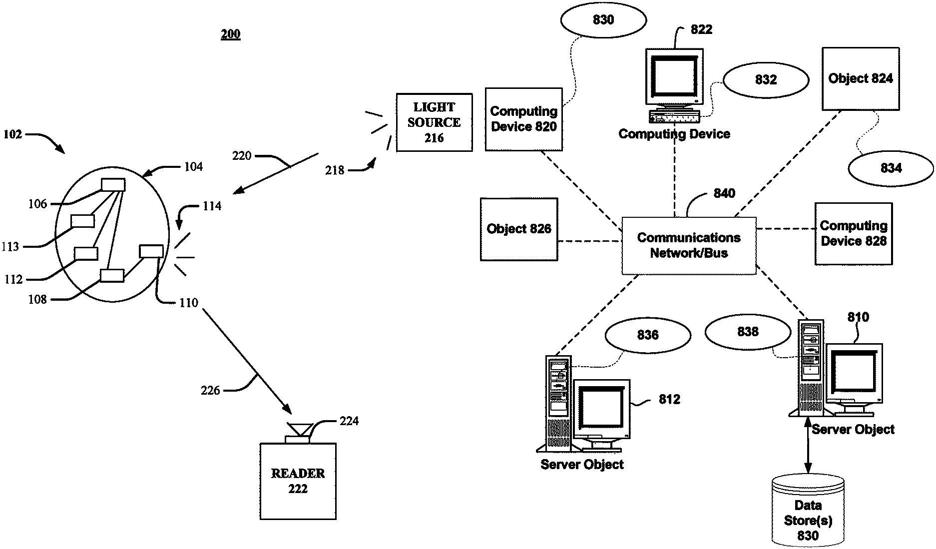
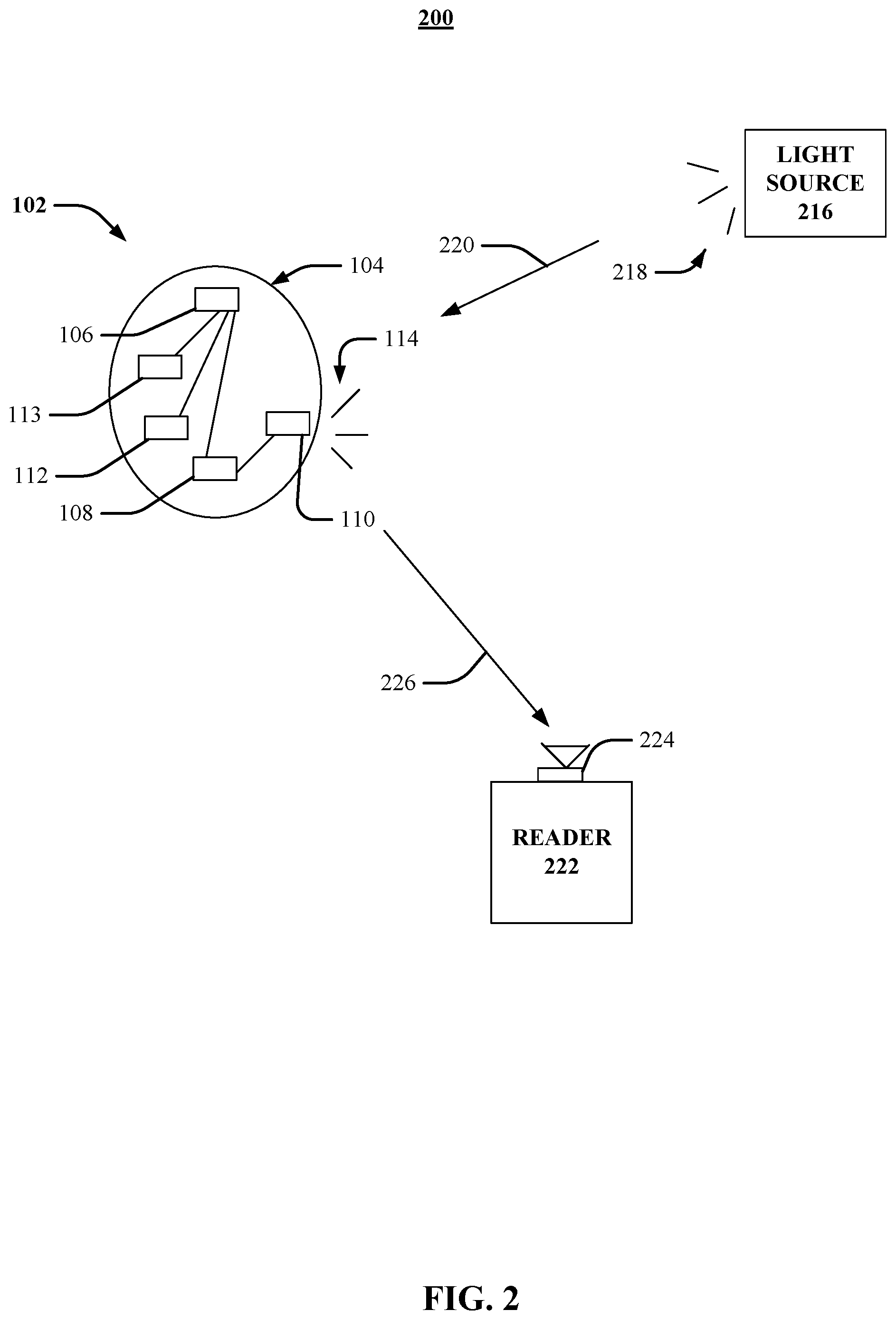
Turning now to FIG. 2, another system that facilitates contact lenses employing optical signals for power and/or communication is shown. System 200 can include contact lens 102, a light source 216 and a reader 222.
The light source 216 can be any number of sources that can generate light (or optical signals generally). By way of example, but not limitation, the light source 216 can be the sun, a source of low-level background light or a device having an optical-signal emitting component such as one above embodiment of device 116 described with reference to FIG. 1. The light source 216 can emit an optical signal 218, 220 that can be received by the contact lens 102. For example, the optical signal 218, 220 can be received by the photodetector 106 as described above with reference to FIG. 1.
The reader 222 can be adapted to receive the modulated signal from the optical communication device 110. For example, the reader 222 can receive the modulated signal at optical-signal receiving component 224 of the reader 222. Optical-signal receiving component 224 can be any number of different types of receivers that can receive and/or sense optical signals. In some aspects, for example, the optical-signal receiving component 224 can include an optical demodulator that is configured to demodulate the modulated signal. The reader 222 can determine the information received based on the pattern with which the signal is modulated by the optical communication device 110.
In some aspects, the contact lens can include the structure and/or function described with reference to FIG. 1. In some aspects, the contact lens 102 can receive optical signal 218, 220 emitted from light source 216 and can output an optical signal 114, 226 to reader 222. For example, the optical communication device 110 can output the optical signal 114, 226 to the reader 222 in response to the output from the sensor 108. The sensor 108 can be powered optically via the optical signal 218, 220 received from the light source 216 as described with reference to FIG. 1.
Accordingly, in various aspects, the contact lens 102 can receive an optical signal 218, 220 from a first source (e.g., light source 216) and output an optical signal 114, 226 to a second source (e.g., reader 222).
Turning now to FIG. 3, another system that facilitates contact lenses employing optical signals for power and/or communication is shown. System 300 can include contact lens 102 and device 316.
The device 316 can be any suitable device that can encode an optical signal 324 with data, and output the optical signal 324. In some aspects, the device 316 can include a data encoder 320 that can encode the optical signal 324, and a light source 318 that can emit the optical signal 324 encoded with the data.
In various aspects, the optical signal 324 can be encoded with data at a rate high enough to avoid detection by the human eye and/or brain. For example, in some aspects, the optical signal 324 can be encoded with data at a rate of 100 bits per second (bps) or greater.
In various aspects, the data can include instructions or information for storage in the memory 113. For example, the data can include instructions for particular features to be sensed by the sensor 108.
The optical signal 324 can be output from the component 322 in some aspects. The optical signal 324 can be received by the contact lens 102. For example, the optical signal 218, 220 can be received by the photodetector 106.
The component 326 can be adapted to receive the modulated signal from the optical communication device 110. Component 326 can be any number of different types of receivers that can receive and/or sense optical signals. The component 326 can determine the information received based on the modulated signal generated by the optical communication device 110. In various aspects, the component 326 can be or include any of a number of different devices having hardware and/or software that transmits and receives an optical signal.
In various aspects, the contact lens can include the structure and/or function described with reference to FIG. 1. In some aspects, the contact lens 102 can receive optical signal 218, 220 emitted from device 316 and can output an optical signal 114 to the device 316. The optical signal 114 can be output from the optical communication device 110 in some aspects. The optical communication device 110 can output the optical signal 114 to the device 316 in response to the output from the sensor 108. The sensor 108 can be powered optically via the optical signal 324 received from the device 316.
While not shown, in other aspects, the systems described herein can include those having contact lens 102, a reader (e.g., reader 222) and/or any device able to emit light (or an optical signal generally).
While not shown, the contact lens can include structure and/or functionality for multi-modal operation. In some aspects, multi-modal operation can mean operating intermittently between RF and optical power modes and/or RF and optical communication modes. For example, in some aspects, the contact lens can employ RF-based power and/or communication and, in other instances, the contact lens can employ optical-based power and/or communication. As another example, optical power and RF communication can be employed. For example, in some aspects, the contact lens can harvest optical energy to power the optical communication device on the contact lens, and harvest RF energy to power an RF device on the contact lens. For example, an RF device can communicate via RF reflection, or backscatter.
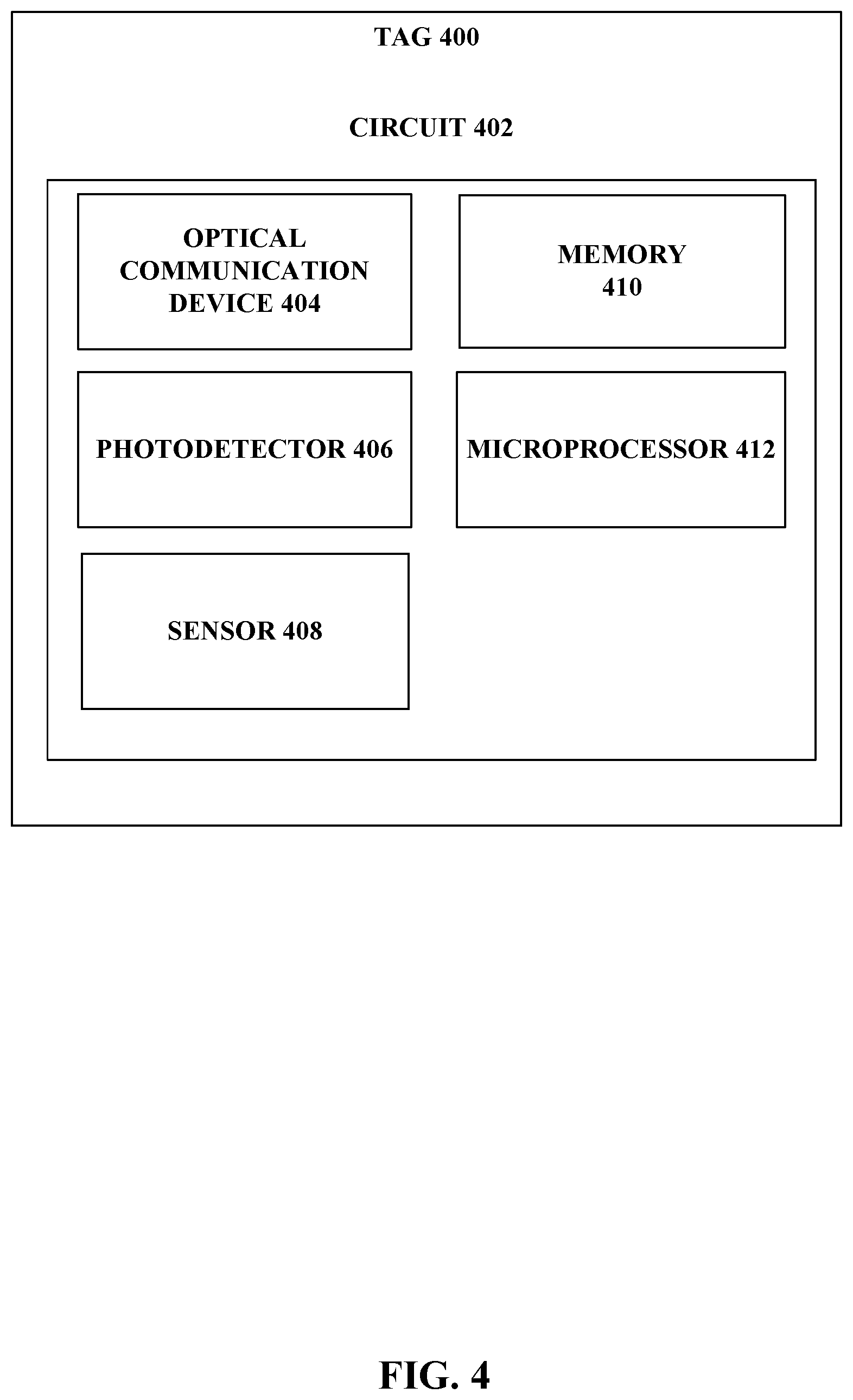
FIG. 4 is an illustration of a block diagram of a tag for a contact lens facilitating optical communication in accordance with aspects described herein. The tag 400 can be disposed on or within the contact lens in various aspects.
The tag 400 can include or be associated with a circuit 402 disposed on or within the tag 400. In some aspects, the circuit 402 can include an optical communication device 404, a photodetector 406, a sensor 408, a memory 410 and/or a microprocessor 412. In various aspects, the optical communication device 404, photodetector 406, sensor 408, memory 410 and/or microprocessor 412 can be optically, electrically and/or communicatively coupled to one another to perform one or more functions of the tag 400. As such, in some aspects, the tag 400 can be configured to have a level of porosity such that fluids incident on the contact lens can be detected and sensing can be performed by the sensor 408. In some aspects, the tag 400 can be transparent or translucent such that the photodetector 406 can receive light for power generation.
In some aspects, the tag 400 can include information identifying the wearer of the contact lens, information stored and/or detailing features of the wearer of the contact lens or the like.
In some aspects, the tag 400 can be associated with an item (e.g., item of merchandise) and/or can be interrogated by a device (e.g., device 116, device 316, reader 222) for merchandising and/or inventory purposes.
For example, in some aspects, a light source can be associated with or coupled to an item of merchandise. The optical signal can be received by the photodetector 406 to power the components of the tag 400, and the tag 400 can output information via the optical communication device 404. The information output by the tag 400 can be communicated via modulation of the optical communication device 404 as described in one or more of the embodiments.
In some aspects, the light source associated with or coupled to the item of merchandise can transmit information about the item to the tag 400 (e.g., by modulating the optical signal with data about the merchandise). For example, the tag 400 can receive information detailing electronic coupons, pricing, warranty information or the like. The information can be received by and/or stored at the memory 410 of the tag 400.
In some aspects, an interrogator (e.g., device 116, device 316, reader 222) at a point of sale can output an optical signal that can cause the tag 400 to responsively output information related to the merchandise. For example, the tag 400 can respond with information indicative of an electronic coupon for the item of merchandise. For example, the interrogator can be operated by a cashier or other point of sale personnel to cause the tag 400 to output an optical signal detailing the terms of the coupon (in response to the tag 400 of the contact lens receiving an optical signal from the interrogator).
In various aspects, the components of the circuit 402 can include the structure and/or functionality of the corresponding components of the contact lens 102 described with reference to FIG. 1. For example, the photodetector 406 can include the structure and/or functionality of photodetector 106 described with reference to FIG. 1.
FIGS. 5, 6 and 7 are exemplary flow diagrams of methods that facilitate contact lenses employing optical signals for power and/or communication in accordance with aspects described herein.
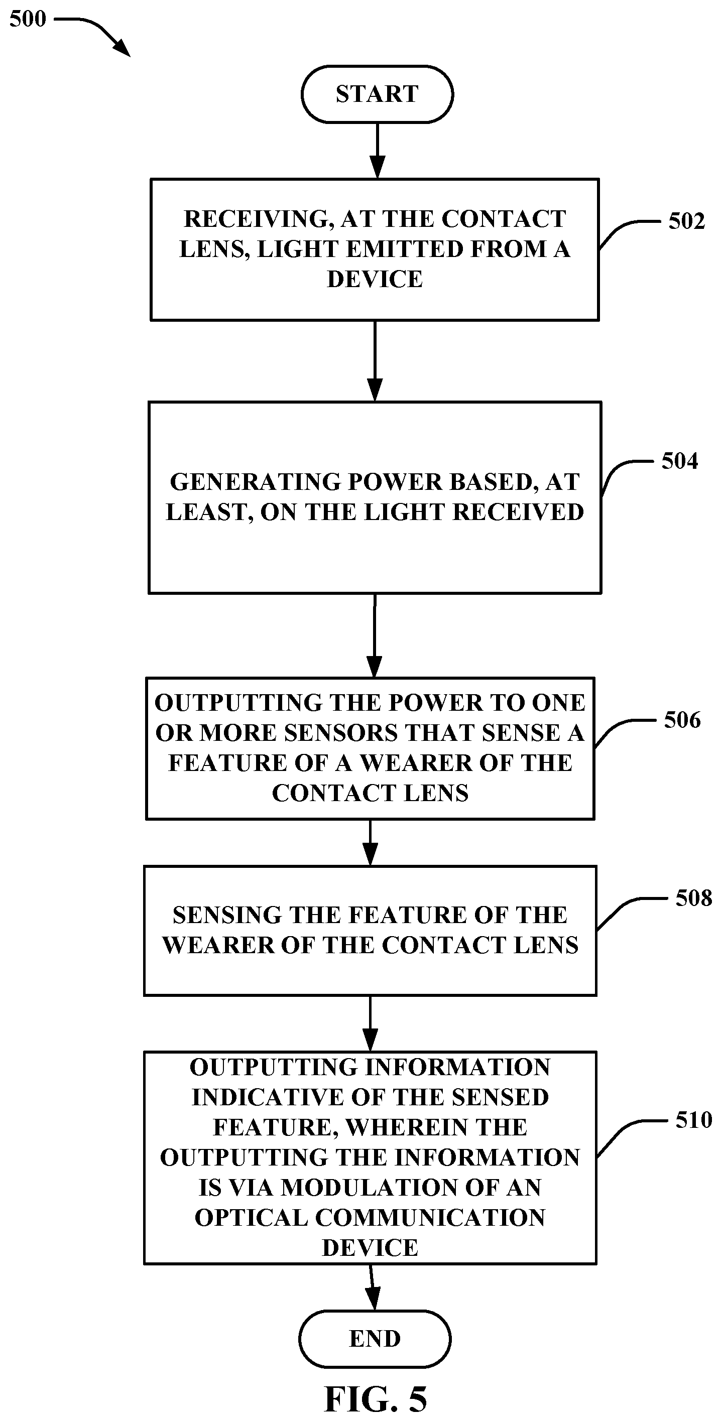
Turning first to FIG. 5, at 502, method 500 can include receiving, at the contact lens, light (or an optical signal, generally) emitted from a device (e.g., using the contact lens 102 or the photodetector 106).
In various aspects, the optical signal can be of a wavelength that is invisible or visible to the human eye. For example, the light can be invisible (e.g., IR light) or other light that is invisible to the human eye but that is detectable by the photodetector or other detector (not shown) on the contact lens 102. For example, while not shown, the systems described herein can include those having a device able to emit IR light signals and a contact lens able to receive and decode IR light signals. The device can include circuitry (e.g., IR transmitter, LED) to emit pulses of IR light. The contact lens can include a receiver that can receive and decode the IR light. The microprocessor of the contact lens can decode data encoded in the IR light in some aspects. In these aspects, the contact lens can perform one or more functions based on the decoded data.
As another example, the light received could be visible light (e.g., a flash from a camera). As another example, the light can be low-level background light or ambient light.
As another example, the light can be modulated with data. The rate at which the light is modulated with the data can be approximately 100 bits per second (bps) or greater. In various aspects, the data with which the light is modulated can include information that can be stored at the contact lens. In various aspects, the data with which the light is modulated can include information that can be employed by the contact lens for one or more functions. For example, the data can be information identifying features for sensing by the sensor of the contact lens and/or information identifying a query for information (e.g., biographical information) to be output from the contact lens.
At 504, method 500 can include generating power based, at least, on the light received (e.g., using the photodetector 106). In various aspects, the power can be harvested by the photodetector and employed to power the sensor on the contact lens. As such, an optical signal can be employed for powering the contact lens.
At 506, method 500 can include outputting the power to one or more sensors that sense a feature of a wearer of the contact lens (e.g., using the photodetector 106).
At 508, method 500 can include sensing the feature of the wearer of the contact lens (e.g., using the sensor 108). The feature can include, but is not limited to, a biological and/or chemical feature of the wearer of the contact lens. In some aspects, although not shown, the method 500 can include sensing a feature of an environment outside of a wearer of the contact lens.
For example, the sensor 108 can sense any number of biological features of the wearer of the contact lens including, but not limited to, glucose, lactate or urea levels, internal body temperature and/or blood alcohol content of the wearer of the contact lens as described in further detail below.
For example, in some aspects, the sensor 108 can detect a fluid on the contact lens output from the eye of the wearer of the contact lens. The sensor 108 can sense a level of glucose, lactate and/or urea in the fluid. In some embodiments, the contact lens can include circuitry for evaluating the level of the substance in the fluid. In some embodiments, the contact lens can include circuitry for outputting the sensed information to a reader. In either aspect, the level of the biological matter can be compared to a threshold. A determination can be made as to whether the level is too high or too low based on the level detected.
As another example, the fluid on the contact lens can be a particular temperature. The temperature of the fluid can be indicative of the internal temperature of the wearer of the contact lens. The sensor 108 can be a temperature sensor that can sense the temperature of the fluid. For example, in some embodiments, the sensor 108 can be a resistance thermometer that detects the temperature based on an increase in resistance (which occurs with a rise in temperature) or a decrease in resistance (which occurs with a decrease in temperature). The sensor 108 can be employed in connection with a thermistor in some embodiments. As another example, the sensor 108 can sense a blood alcohol content of the wearer of the contact lens. In particular, the sensor 108 can detect the fluid incident on the contact lens. For example, the tear film of the eye can be incident on the contact lens. The alcohol concentration in the tear film can be sensed by sensor 108.
In some aspects, the sensor 108 can sense one or more features in an environment outside of the wearer of the contact lens. For example, the sensor 108 can sense any number of biological, chemical and/or microbiological features in an environment including, but not limited to, levels of hazardous materials, levels of allergens, the presence of various organisms or species or the like. For example, in various embodiments, the sensor 108 can sense a level of one or more different allergens (e.g., tree or grass pollen, pet dander, dust mite excretions) in the environment. At 510, method 500 can include outputting information indicative of the sensed feature (e.g., using the optical communication device 110). In various aspects, the information can be output from the optical communication device via modulation of the optical communication device. For example, the manner in which the optical communication device is modulated can communicate the details of the information sensed.
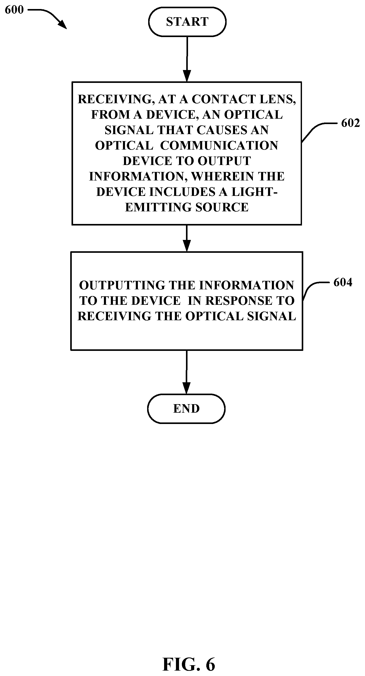
Turning now to FIG. 6, at 602, method 600 can include receiving, at a contact lens, from a device, an optical signal that causes an optical communication device to output information (e.g., using the photodetector 106 of the contact lens 102). In some aspects, the device can include a light-emitting source.
At 604, method 600 can include outputting the information to the device (e.g., using the optical communication device 110 of the contact lens 102).
Turning now to FIG. 7, at 702, method 700 can include receiving, at a contact lens, from a light-emitting source, an optical signal that causes an optical communication device to output information (e.g., using the photodetector 106 of the contact lens 102).
In various aspects, the light-emitting source can be a device that emits optical signals. For example, the light-emitting source can be a camera having a component that generates a flash of light. In some aspects, the light-emitting source can be a source of ambient light (e.g., sun) or a source of low-level background light. In some aspects, the light-emitting source can also include structure for modulating the light output with data. As such, the light emitted can include data.
At 704, method 700 can include outputting the information to a light-receiving device (e.g., using the optical communication device 110 of the contact lens 102). In various aspects, the light-receiving device can be a device that receives and reads optical signals. In some aspects, the light-emitting source is distinct from the light-receiving device. As such, the contact lens can receive an optical signal from a first source and emit optical signals to a second source.
Exemplary Networked and Distributed Environments
FIG. 8 provides a schematic diagram of an exemplary networked or distributed computing environment with which one or more aspects described in this disclosure can be associated. The distributed computing environment includes computing objects 810, 812, etc. and computing objects or devices 820, 822, 824, 826, 828, etc., which can include programs, methods, data stores, programmable logic, etc., as represented by applications 830, 832, 834, 836, 838. It can be appreciated that computing objects 810, 812, etc. and computing objects or devices 820, 822, 824, 826, 828, etc. can include different devices, such as active contact lenses (and components thereof), personal digital assistants (PDAs), audio/video devices, mobile phones, MPEG-1 Audio Layer 3 (MP3) players, personal computers, laptops, tablets, etc.
Each computing object 810, 812, etc. and computing objects or devices 820, 822, 824, 826, 828, etc. can communicate with one or more other computing objects 810, 812, etc. and computing objects or devices 820, 822, 824, 826, 828, etc. by way of the communications network 840, either directly or indirectly. Even though illustrated as a single element in FIG. 8, network 840 can include other computing objects and computing devices that provide services to the system of FIG. 8, and/or can represent multiple interconnected networks, which are not shown.
In a network environment in which the communications network/bus 840 can be the Internet, the computing objects 810, 812, etc. can be Web servers, file servers, media servers, etc. with which the client computing objects or devices 820, 822, 824, 826, 828, etc. communicate via any of a number of known protocols, such as the hypertext transfer protocol (HTTP).
Exemplary Computing Device
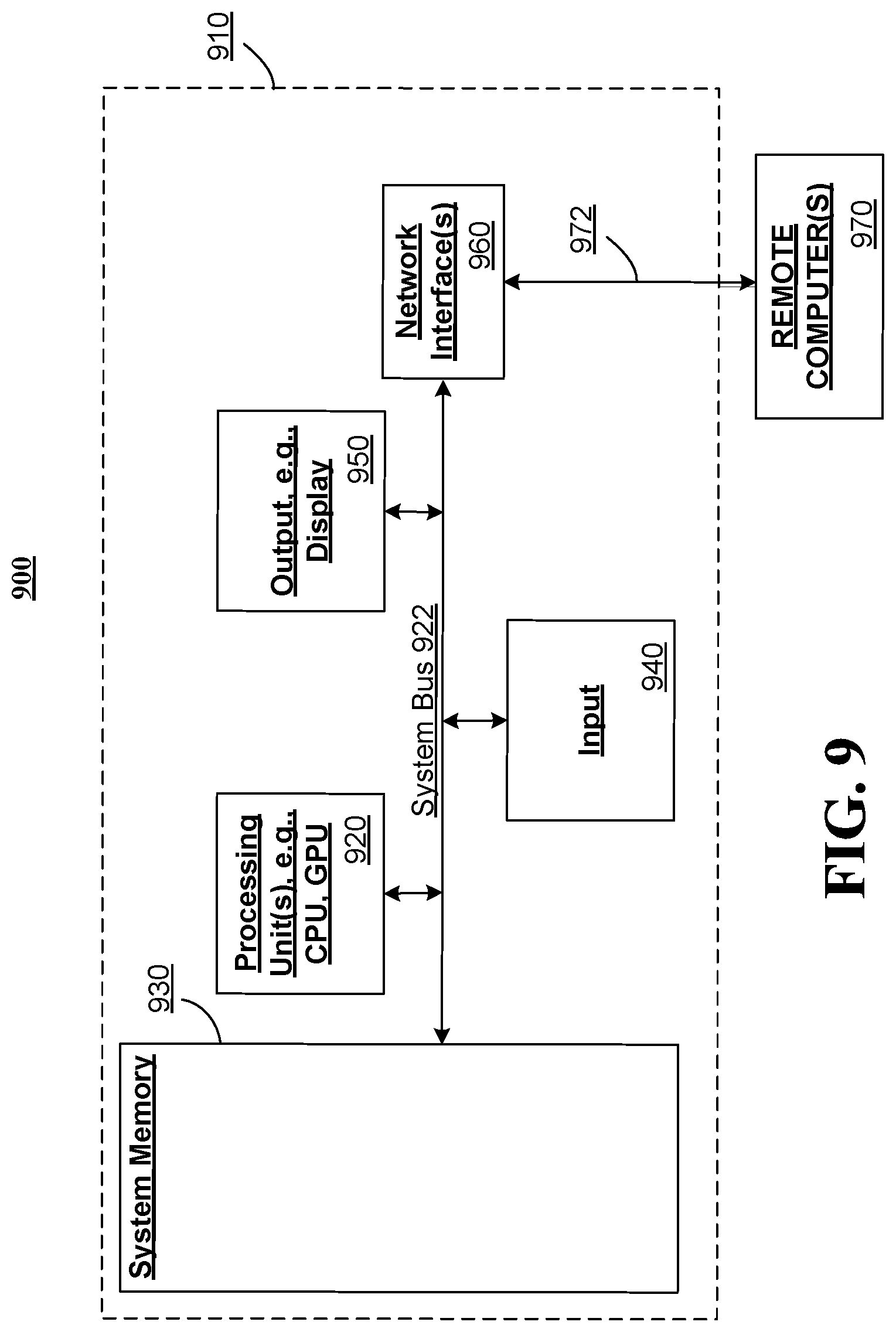
As mentioned, advantageously, the techniques described in this disclosure can be associated with any suitable device. It is to be understood, therefore, that handheld, portable and other computing devices (including active contact lens having circuitry or components that compute and/or perform various functions). As described, in some aspects, the device can be the contact lens (or components of the contact lens) and/or reader described herein. In various aspects, the data store can include or be included within, any of the memory described herein, any of the contact lenses described herein and/or the RF reader described herein. In various aspects, the data store can be any repository for storing information transmitted to or received from the contact lens.
FIG. 9 illustrates an example of a suitable computing system environment 900 in which one or aspects of the aspects described in this disclosure can be implemented. Components of computer 910 can include, but are not limited to, a processing unit 920, a system memory 930, and a system bus 922 that couples various system components including the system memory to the processing unit 920.
Computer 910 typically includes a variety of computer readable media and can be any available media that can be accessed by computer 910. The system memory 930 can include computer storage media in the form of volatile and/or nonvolatile memory such as read only memory (ROM) and/or random access memory (RAM). By way of example, and not limitation, memory 930 can also include an operating system, application programs, other program components, and program data.
A user can enter commands and information into the computer 910 through input devices 940 (e.g., keyboard, keypad, a pointing device, a mouse, stylus, touchpad, touch screen, motion detector, camera, microphone or any other device that allows the user to interact with the computer 910). A monitor or other type of display device can be also connected to the system bus 922 via an interface, such as output interface 950. In addition to a monitor, computers can also include other peripheral output devices such as speakers and a printer, which can be connected through output interface 950.
The computer 910 can operate in a networked or distributed environment using logical connections to one or more other remote computers, such as remote computer 980. The remote computer 980 can be a personal computer, a server, a router, a network PC, a peer device or other common network node, or any other remote media consumption or transmission device, and can include any or all of the elements described above relative to the computer 910. The logical connections depicted in FIG. 9 include a network 982, such local area network (LAN) or a wide area network (WAN), but can also include other networks/buses e.g., cellular networks.
Computing devices typically include a variety of media, which can include computer-readable storage media and/or communications media, in which these two terms are used herein differently from one another as follows. Computer-readable storage media can be any available storage media that can be accessed by the computer, can be typically of a non-transitory nature, and can include both volatile and nonvolatile media, removable and non-removable media. By way of example, and not limitation, computer-readable storage media can be implemented in connection with any method or technology for storage of information such as computer-readable instructions, program components, structured data, or unstructured data. Computer-readable storage media can include, but are not limited to, RAM, ROM, electrically erasable programmable read only memory (EEPROM), flash memory or other memory technology, or other tangible and/or non-transitory media which can be used to store desired information. Computer-readable storage media can be accessed by one or more local or remote computing devices, e.g., via access requests, queries or other data retrieval protocols, for a variety of operations with respect to the information stored by the medium. In various aspects, the computer-readable storage media can be, or be included within, the memory, contact lens (or components thereof) or reader described herein.
On the other hand, communications media typically embody computer-readable instructions, data structures, program components or other structured or unstructured data in a data signal such as a modulated data signal, e.g., a carrier wave or other transport mechanism, and includes any information delivery or transport media. The term "modulated data signal" or signals refers to a signal that has one or more of its characteristics set or changed in such a manner as to encode information in one or more signals.
It is to be understood that the aspects described in this disclosure can be implemented in hardware, software, firmware, middleware, microcode, or any combination thereof. For a hardware aspect, the processing units can be implemented within one or more application specific integrated circuits (ASICs), digital signal processors (DSPs), digital signal processing devices (DSPDs), programmable logic devices (PLDs), field programmable gate arrays (FPGAs), processors, controllers, micro-controllers, microprocessors and/or other electronic units designed to perform the functions described in this disclosure, or a combination thereof.
For a software aspect, the techniques described in this disclosure can be implemented with components or components (e.g., procedures, functions, and so on) that perform the functions described in this disclosure. The software codes can be stored in memory units and executed by processors.
What has been described above includes examples of one or more aspects. It is, of course, not possible to describe every conceivable combination of components or methodologies for purposes of describing the aforementioned aspects, but one of ordinary skill in the art can recognize that many further combinations and permutations of various aspects are possible. Accordingly, the described aspects are intended to embrace all such alterations, modifications and variations that fall within the spirit and scope of the appended claims.
Moreover, the term "or" is intended to mean an inclusive "or" rather than an exclusive "or." That is, unless specified otherwise, or clear from the context, the phrase "X employs A or B" is intended to mean any of the natural inclusive permutations. That is, the phrase "X employs A or B" is satisfied by any of the following instances: X employs A; X employs B; or X employs both A and B. In addition, the articles "a" and "an" as used in this application and the appended claims should generally be construed to mean "one or more" unless specified otherwise or clear from the context to be directed to a singular form.
The aforementioned systems have been described with respect to interaction between several components. It can be appreciated that such systems and components can include those components or specified sub-components. Sub-components can also be implemented as components communicatively coupled to other components rather than included within parent components (hierarchical). Additionally, it is to be noted that one or more components can be combined into a single component providing aggregate functionality. Any components described in this disclosure can also interact with one or more other components not specifically described in this disclosure but generally known by those of skill in the art.
In view of the exemplary systems described above methodologies that can be implemented in accordance with the described subject matter will be better appreciated with reference to the flowcharts of the various figures. While for purposes of simplicity of explanation, the methodologies are shown and described as a series of blocks, it is to be understood and appreciated that the claimed subject matter is not limited by the order of the blocks, as some blocks can occur in different orders and/or concurrently with other blocks from what is depicted and described in this disclosure. Where non-sequential, or branched, flow is illustrated via flowchart, it can be appreciated that various other branches, flow paths, and orders of the blocks, can be implemented which achieve the same or a similar result. Moreover, not all illustrated blocks may be required to implement the methodologies described in this disclosure after.
In addition to the various aspects described in this disclosure, it is to be understood that other similar aspects can be used or modifications and additions can be made to the described aspect(s) for performing the same or equivalent function of the corresponding aspect(s) without deviating there from. Still further, multiple processing chips or multiple devices can share the performance of one or more functions described in this disclosure, and similarly, storage can be provided across a plurality of devices. The invention is not to be limited to any single aspect, but rather can be construed in breadth, spirit and scope in accordance with the appended claims.
* * * * *
References
- /economist.com/node/18750624/print
-
gizmag.com/microsoft-electronic-diabetic-contact-lens/20987
-
patexia.com/feed/active-contactlens-that-lets-you-see-like-the-terminator-patented-2407
-
spectrumieee.org/biomedical/bionics/augmented-reality-in-a-contact-lens/0
-
kurzweilai.net/forums/topic/bionic-contact-lens-to-project-emailsbefore-eyes
-
ksi.edu/seke/dms11/DMS/2_Kohji_Mitsubayashi.pdf
-
dailymail.co.uk/health/article-1267345/How-contact-lenses-help-save-life.htrnl
D00000
D00001
D00002
D00003
D00004
D00005
D00006
D00007
D00008
D00009
XML
uspto.report is an independent third-party trademark research tool that is not affiliated, endorsed, or sponsored by the United States Patent and Trademark Office (USPTO) or any other governmental organization. The information provided by uspto.report is based on publicly available data at the time of writing and is intended for informational purposes only.
While we strive to provide accurate and up-to-date information, we do not guarantee the accuracy, completeness, reliability, or suitability of the information displayed on this site. The use of this site is at your own risk. Any reliance you place on such information is therefore strictly at your own risk.
All official trademark data, including owner information, should be verified by visiting the official USPTO website at www.uspto.gov. This site is not intended to replace professional legal advice and should not be used as a substitute for consulting with a legal professional who is knowledgeable about trademark law.