Metal oxide based radiation sensor
Alodhayb , et al. December 22, 2
U.S. patent number 10,871,580 [Application Number 16/923,725] was granted by the patent office on 2020-12-22 for metal oxide based radiation sensor. This patent grant is currently assigned to KING SAUD UNIVERSITY. The grantee listed for this patent is KING SAUD UNIVERSITY. Invention is credited to Hamad Abdulaziz Albrithen, Abdullah Nasser Alodhayb, Khaled Zouher Shamma.


View All Diagrams
| United States Patent | 10,871,580 |
| Alodhayb , et al. | December 22, 2020 |
Metal oxide based radiation sensor
Abstract
A metal oxide based radiation sensor includes a titanium dioxide (TiO.sub.2) thin film layer on a microcantilever surface. The TiO.sub.2 thin film layer initially comprises anatase and rutile crystal structures. Exposure to radiation, such as gamma radiation, results in changes in structural features and mechanical behaviors of the metal oxide based radiation sensor. In particular, the resonant frequency changes with exposure to radiation dosages. The structural and mechanical behaviors of the metal oxide based radiation sensor change proportionally with dosage within a range of dosages.
| Inventors: | Alodhayb; Abdullah Nasser (Riyadh, SA), Albrithen; Hamad Abdulaziz (Riyadh, SA), Shamma; Khaled Zouher (Riyadh, SA) | ||||||||||
|---|---|---|---|---|---|---|---|---|---|---|---|
| Applicant: |
|
||||||||||
| Assignee: | KING SAUD UNIVERSITY (Riyadh,
SA) |
||||||||||
| Family ID: | 1000004971262 | ||||||||||
| Appl. No.: | 16/923,725 | ||||||||||
| Filed: | July 8, 2020 |
| Current U.S. Class: | 1/1 |
| Current CPC Class: | G01T 1/1606 (20130101) |
| Current International Class: | G01T 1/16 (20060101) |
References Cited [Referenced By]
U.S. Patent Documents
| 5760402 | June 1998 | Hug |
| 2004/0223884 | November 2004 | Chen |
| 2004/0235296 | November 2004 | Bailey et al. |
| 2006/0180756 | August 2006 | Williford |
| 2020/0240836 | July 2020 | Becker |
| 101303239 | Nov 2008 | CN | |||
| 101718667 | Jun 2010 | CN | |||
| 101738355 | Jun 2010 | CN | |||
Other References
|
S Mansoor. Gamma induced effects on structual, optical and electrical properties of n-TiO2/p-Si heterojunction. J Mater Sci: Mater Electron (2017) 28:16314-16320. cited by applicant. |
Primary Examiner: Taningco; Marcus H
Attorney, Agent or Firm: Nath, Goldberg & Meyer Litman; Richard C.
Claims
We claim:
1. A radiation sensor comprising: a substrate; a microcantilever having one end operatively coupled to the substrate; and a metal oxide layer arranged on a surface of the microcantiever, wherein the metal oxide layer comprises the metal oxide in at least one crystal form, the at least one crystal form being capable of transformation to a different form upon exposure to a radiation to be detected.
2. The radiation sensor of claim 1, wherein the metal oxide is titanium dioxide.
3. The radiation sensor of claim 2, wherein the at least one crystal form includes rutile.
4. The radiation sensor of claim 2, wherein the at least one crystal form includes rutile and anatase.
5. The radiation sensor of claim 2, wherein the microcantilever comprises a silicon based material.
6. The radiation sensor of claim 5, wherein the metal oxide layer has a first average thickness in a direction normal to the surface of the microcantilever on which the metal oxide layer is arranged and the microcantilever has a second average thickness in said direction, and the ratio of the first thickness to the second thickness is between 1:50 and 1:1.
7. The radiation sensor of claim 6 wherein the ratio of the first thickness to the second thickness is between 1:20 and 1:5.
8. The radiation sensor of claim 1, wherein the first thickness is uniform over the surface of the microcantilever on which the metal oxide layer is arranged.
9. The radiation sensor of claim 1, wherein the metal oxide layer comprises crystal grains having an initial grain size before exposure to the radiation to be detected and the crystal grains have a second grain size after exposure to the radiation to be detected, wherein the second grain size is smaller than the initial grain size.
10. A device comprising the radiation sensor of claim 1 and a structure for immobilizing the radiation sensor and enclosing the radiation sensor, the chamber being penetrable to the radiation to be detected.
11. The device of claim 10, wherein the chamber is configured to be worn on a person.
12. A method for detecting radiation exposure comprising steps of: measuring a detectable quantity of radiation in the radiation sensor of claim 1 to get a base value; exposing the radiation sensor to radiation; measuring the detectable quantity of radiation exposed to the radiation sensor to get an exposed value; and calculating a difference between the base value and the exposed value as a change in the detectable quantity of the radiation sensor.
13. The method of claim 12, wherein the detectable quantity is the resonant frequency of the microcantilever.
14. A method of fabricating a radiation sensor comprising: providing a microcantilever having one end coupled to a substrate; and coating a side of the microcantilever with a metal oxide layer, wherein the metal oxide layer comprises the metal oxide in at least one crystal form, the at least one crystal form being capable of transformation to a different form upon exposure to a radiation to be detected.
15. The method of claim 14, wherein the metal oxide layer is coated on the side of the microcantilever by means of atomic layer deposition.
16. The method of claim 14, wherein the metal oxide layer ranges from about 50 to about 200 nm thick.
Description
BACKGROUND
1. Field
The disclosure of the present patent application relates to a system for radiation detection and method of detecting. In particular, the disclosure relates to a system comprising metal oxide thin film layers on a micro-cantilever sensitive to radiation exposure.
2. Description of the Related Art
Micro-Eectro-Mechanical Systems (MMS) are miniature machines having a mechanical and electrical component. MEMS are typically small enough to fit on a typical computer chip as a component in the chip circuitry and have dimensions on the order of millimeters, microns or nanometers, depending on application. Micromechanical resonators, such as microcantilevers as sensors, have been utilized in many physical, chemical and medical applications. Various sensing mechanisms have been used to transduce MEMS sensor signals, such as piezoresistance, piezoelectricity, optical modulation, gyroscope principles, capacitance, frequency shift and pressure.
MEMS devices are sensitive to mechanical stress. MEMS-based resonators and cantilevers are capable of ultra-sensitive mass detection, including masses in the atto- to zeptogram ranges. Such MEMS-based sensors can be batch produced using conventional micromachining techniques and offer reduced size, high precision and increased reliability compared to conventional sensors.
Gamma radiation is deeply penetrating and highly energetic electromagnetic radiation. Gamma radiation interaction with materials causes ionization and introduces defects into atomic lattices by atomic displacement. Radiation exposure can affect electrical, optical and physical properties of materials. For example, radiant energy interaction with matter is very important in research or measurement applications, since microstructural properties of matter are changed when exposed to ionizing radiation. The International Commission on Radiological Protection (ICRP) provides a system and useful standards for radiation protection, including medical, occupational, environmental and exposure controls against radiological accidents without unduly limiting the beneficial practices giving rise to radiation exposure. Thus, there exists a significant demand for practical, accurate and portable devices for detection of radiation.
TiO.sub.2 films have useful and well-understood optical, electrical, physical and chemical properties. TiO.sub.2 films are also inexpensive, nontoxic, highly stable, simple to prepare, transparent to visible light, photocatalytic, useful for electron transport and high in refractive index. Moreover, TiO.sub.2 is suitable for applications in ceramic membranes, gas sensors, optical filters, antireflection coatings and photocatalysts. The crystalline structure of TiO.sub.2 has three phases: anatase, rutile and brookite. Anatase and rutile each have a tetragonal structure, and brookite, has an orthorhombic structure. TiO.sub.2 films may be prepared by various known techniques, including atomic layer deposition, which allows for deposition of TiO.sub.2 thin films on substrates with sub-nanometer precision in material thickness, high quality and excellent atomic level control of layer uniformity.
A radiation sensor is desired to solve the aforementioned problems.
SUMMARY
A radiation sensor, described herein as an embodiment of the present subject matter, comprises a substrate, a microcantilever having one end operatively coupled to the substrate; and a metal oxide layer arranged on a surface of the microcantilever, wherein the metal oxide layer comprises the metal oxide in at least one crystal form, the at least one crystal form being capable of transformation to a different form upon exposure to a radiation to be detected. When the radiation sensor is exposed to the radiation to be detected with a dosage within a detectable dosage range, an initial resonant frequency of the microcantilever with the metal oxide layer is shifted by a frequency shift to a second resonant frequency.
Other embodiments include a method of fabricating a radiation sensor of the present specification and methods of using such a radiation sensor to detect radiation and as a dosimeter.
These and other features of the present subject matter will become readily apparent upon further review of the following specification.
BRIEF DESCRIPTION OF THE DRAWINGS
FIG. 1 depicts XRD patterns of the TiO.sub.2 thin films on Si substrate produced by ALD at 200.degree. C.: (as-deposited) 0 kGy, 10 kGy, 20 kGy, 30 kGy and 40 kGy.
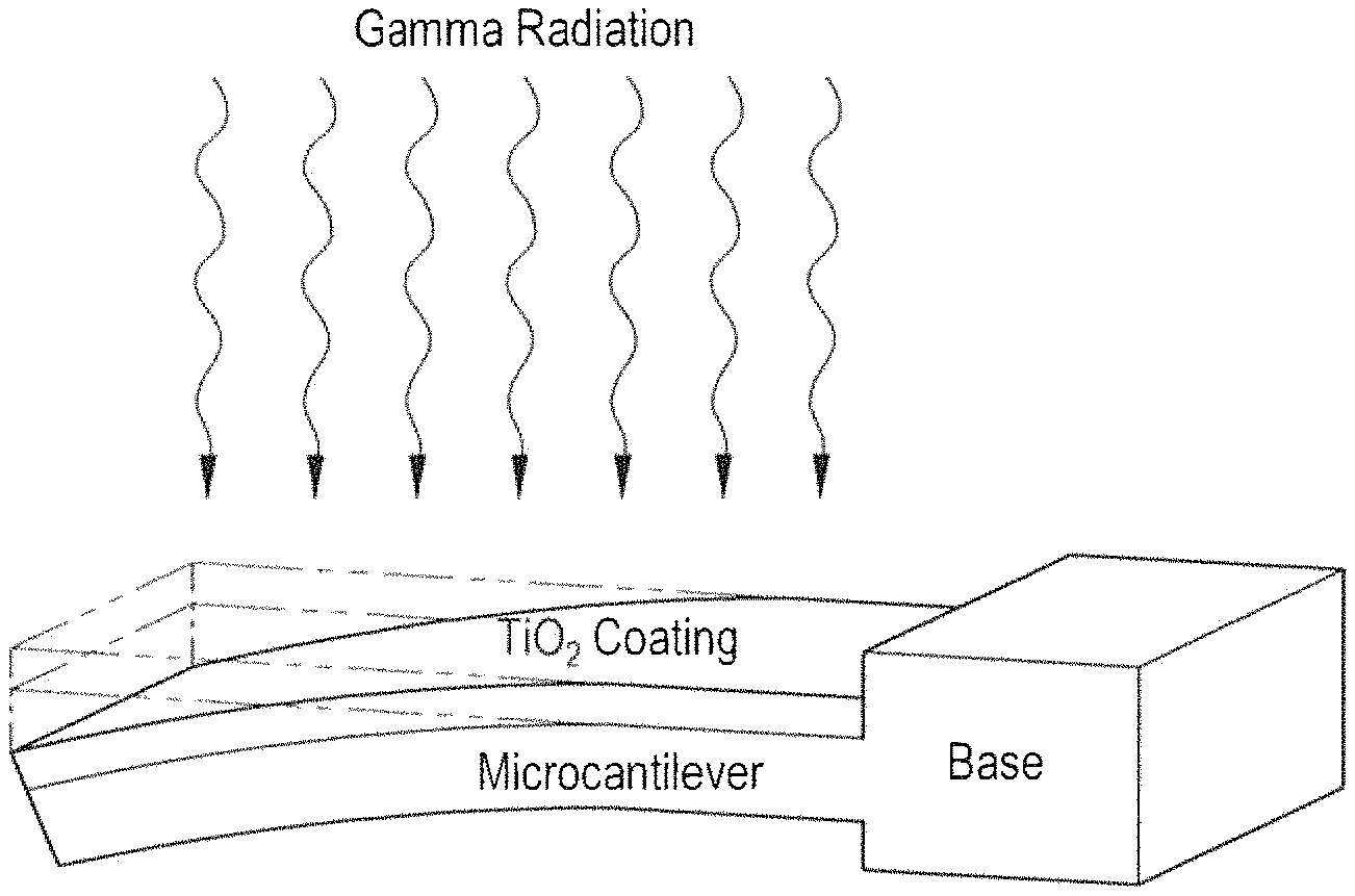
FIG. 2 provides a scheme of the proposed sensor mechanism of the TiO.sub.2 thin film coated surface microcantilever.
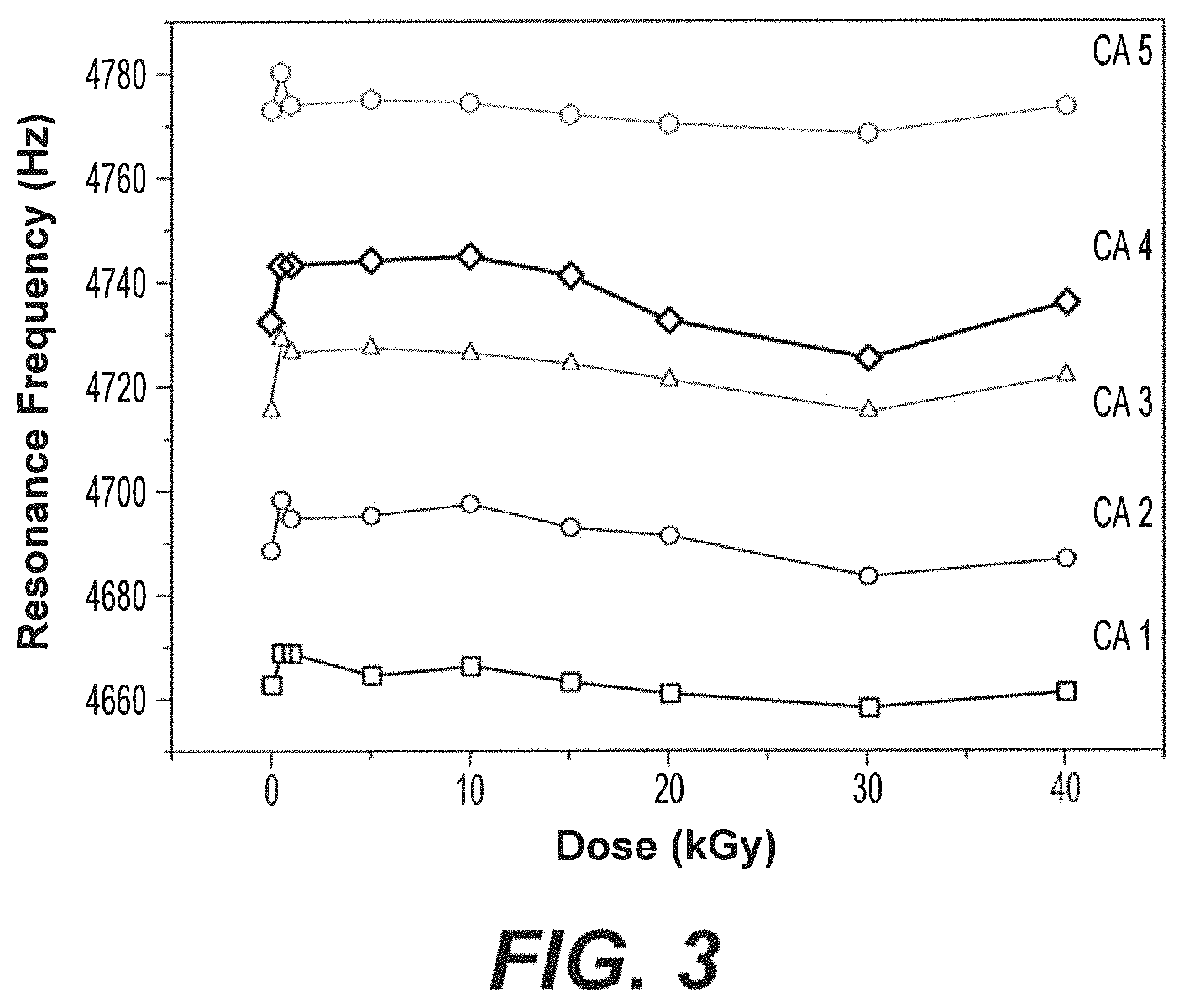
FIG. 3 shows resonant frequencies of Si microcantilevers (CA1-5) without a TiO.sub.2 thin film coating layer under varying gamma irradiation doses.
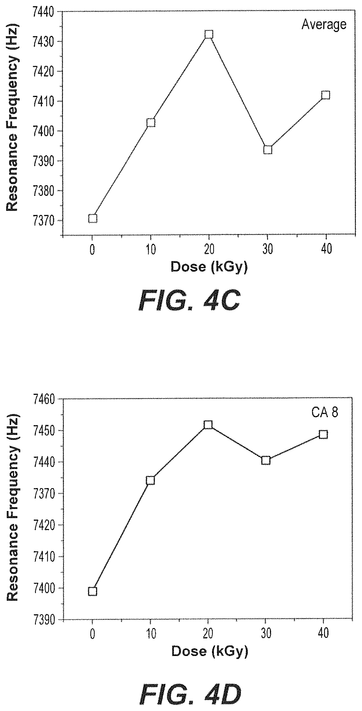
FIGS. 4A-4D show resonant frequencies of TiO.sub.2 thin film coated Si microcantilevers for CA6 (FIG. 4A), for CA7 (FIG. 413), for CA8 (FIG. 4D) and the average thereof (FIG. 4C) under gamma irradiation doses from 0-40 kGy.
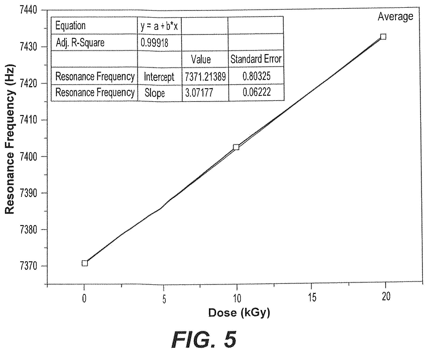
FIG. 5 shows resonant frequencies of TiO.sub.2 thin film coated Si microcantilevers (CA6-8) and the average thereof under gamma irradiation doses from 0-20 kGy with a best fit trend line.
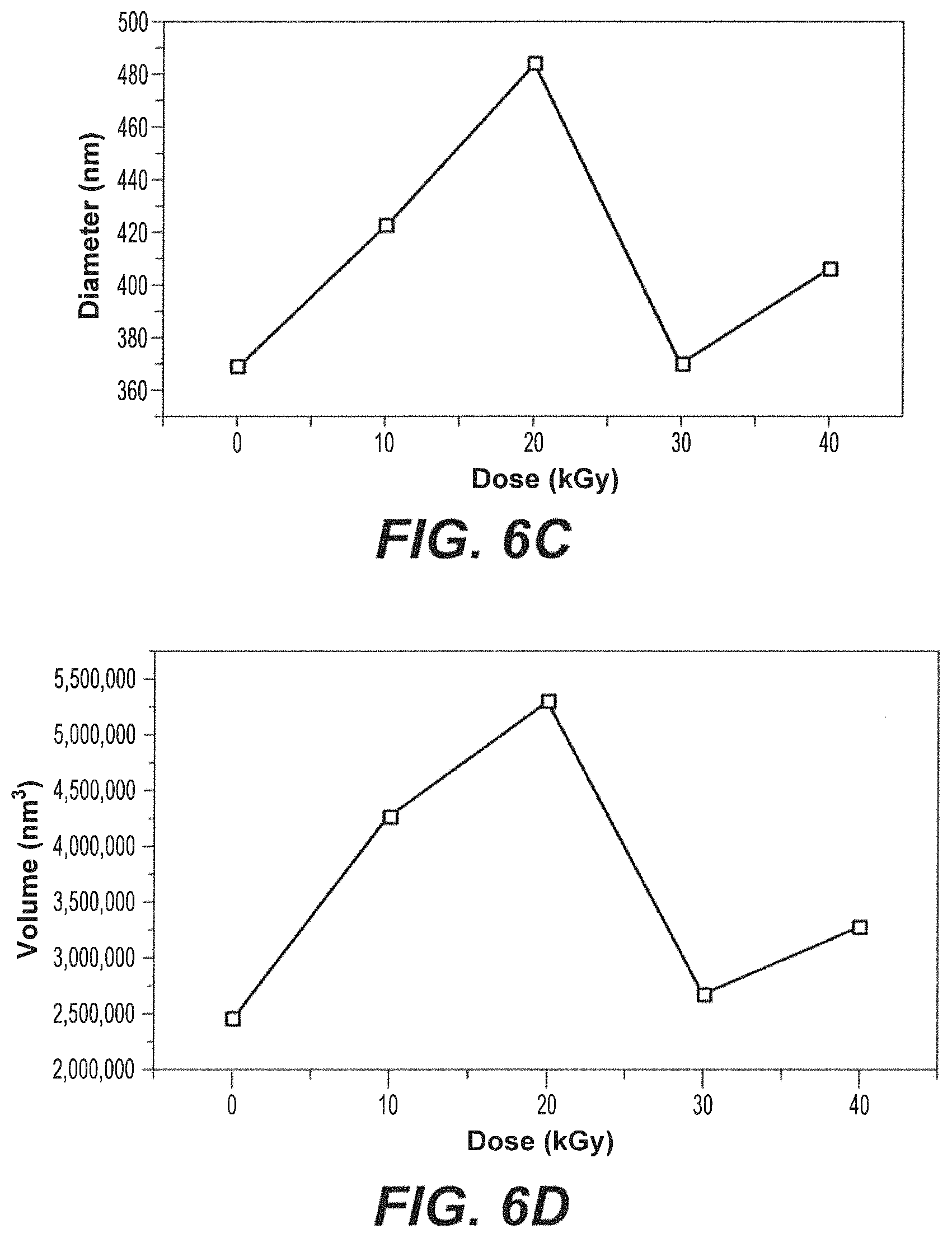
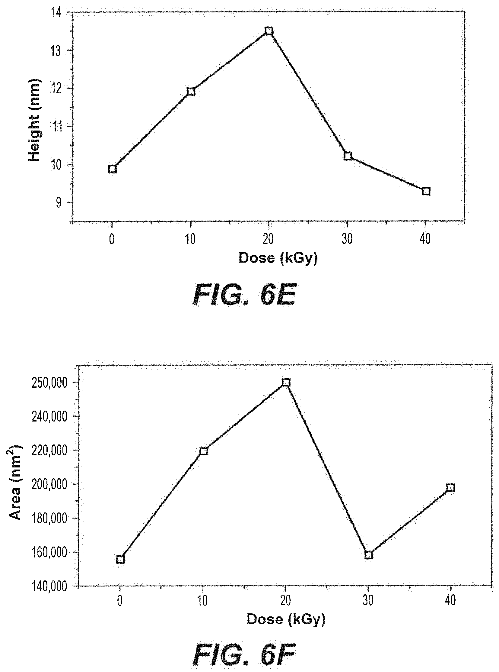
FIGS. 6A-6F show length (FIG. 6A), breadth (FIG. 6B), diameter (FIG. 6C), volume (FIG. 6D), height (FIG. 6E) and area (FIG. 6F), calculated from AFM images of TiO.sub.2 thin films on Si substrates subject to radiation doses of 0 kGy (as-deposited), 10 kGy, 20 kGy, 30 kGy and 40 kGy.
FIGS. 7A-7C show SEM micrographs of TiO.sub.2 thin films on silicon wafers after radiation doses of 0 kGy (as-deposited) (FIG. 7A); 10 kGy (FIG. 7B); and 20 kGy (FIG. 7C).
FIG. 8 is the refractive index (extracted from spectroscopic ellipsometry) for Si wafers, without TiO.sub.2 thin film coating TiO.sub.2, at radiation doses of 0 kGy, 1 kGy, 10 kGy and 20 kGy.
FIG. 9 shows changes in measured thickness of the native SiO.sub.2 layer of uncoated silicon wafers, measured by spectroscopic ellipsometry, and resonant frequency of uncoated microcantilevers, determined by AFM (inset in FIG. 9 is FIG. 3).
FIGS. 10A-10B depict spectroscopic ellipsometric measurements of .PSI. (FIG. 10A) and A in degrees vs. wavelength (FIG. 10B) for TiO.sub.2 thin films on Si wafers after 10 kGy radiation at an angle of incidence of 65 and 75 (inset in FIG. 10B shows the layering model used to analyze the ellipsometric data).
FIG. 11 depicts the dispersion spectra of the refractive index of the bottom layer of TiO.sub.2 thin films on Si wafers with different radiation doses of 0 kGy, 10 kGy, 20 kGy, 30 kGy and 40 kGy (inset in FIG. 11 includes the average data shown in FIG. 4).
FIG. 12 depicts TiO.sub.2 thin film thickness and the roughness following radiation doses of 0 kGy, 10 kGy, 20 kGy, 30 kGy and 40 kGy for TiO.sub.2 thin films on silicon wafers determined by AFM.
FIG. 13 depicts the thickness measurements of FIG. 12 with resonant frequency shifts of TiO.sub.2 thin film coated microcantilevers measured by AFM.
Similar reference characters denote corresponding features consistently throughout the attached drawings.
DETAILED DESCRIPTION OF THE PREFERRED EMBODIMENTS
An embodiment of the present specification is directed to a radiation sensor, shown in FIG. 2, for detecting radiation. The radiation sensor can include a substrate or base, a microcantilever having one end in communication with the substrate, and a metal oxide layer arranged on a surface of the microcantilever. The metal oxide layer can include the metal oxide in at least one crystal form. The at least one crystal form can be capable of transformation to a different form upon exposure to the radiation. When the radiation sensor is exposed to the radiation within a detectable dosage range, an initial resonant frequency of the microcantilever with the metal oxide layer is shifted by a frequency shift to a second resonant frequency. In an embodiment, the metal oxide is titanium dioxide. The at least one crystal form may include rutile, anatase, or both rutile and anatase. In an embodiment, the microcantilever comprises a silicon based material.
In an embodiment, the metal oxide layer has a first average thickness in a direction normal to the surface of the microcantilever on which the metal oxide layer is arranged and the microcantilever has a second average thickness in said direction, and the ratio of the first thickness to the second thickness is between 1:50 and 1:1. In another embodiment, the ratio of the first thickness to the second thickness is between 1:20 and 1:5. The metal oxide layer may be arranged on a part or entirety of a surface of the microcantilever. The metal oxide layer has, in an embodiment, uniform thickness over the surface of the microcantilever on which the metal oxide layer is disposed. The absolute dimensions of the microcantilever and metal oxide layer can be such that the resonant frequency of the microcantilever with metal oxide layer is sensitive to changes due to loss of the metal oxide layer.
The microcantilever is not particularly limited in shape. In one embodiment, the microcantilever is a rectangular prism with a width, length and second average thickness. In this case, the resonant frequency is approximated according to: .omega..sub.0=(k/m).sup.1/2, where k=Et.sup.3w/4].sup.3
where resonant frequency (.omega..sub.0) of the bare microcantilever is related to its spring constant (k) and mass (m). E=Young's modulus of Elasticity (a property of the microcantilever material), t=thickness, w=width, and l=length. The dimensions t, w and l of the microcantilever can be chosen such that k above is on the order of the mass of metal oxide arranged on the microcantilever. In particular embodiments, the length of the microcantilever is on the order of mm, i.e., 0.1-10 mm, 0.5-5 mm or 0.5-1 mm. The width of the microcantilever is 10-1000 microns, 50-500 microns or 50-100 microns; and the thickness of the microcantilever is 0.5-10 microns or 1-5 microns. The metal oxide layer may be 10-1000 microns thick, 50-500 microns thick, or 50-200 microns thick.
In an embodiment, the metal oxide layer comprises crystal grains having an initial grain size before exposure to the radiation to be detected and the crystal grains have a second grain size after exposure to the radiation to be detected, wherein the second grain size is smaller than the initial grain size. The crystal grain size may be determined by any typical means of observing and calculating an average grain size, for example by XRD and calculating an average grain size using Scherrer's formula, as will be discussed below, or else direct imaging by SEM, TEM or AFM, for example, and calculating an average area of observed crystal grains.
In another embodiment of the radiation sensor, exposing the radiation sensor to the radiation of a first dosage or a second dosage results in a first frequency shift or a second frequency shift, respectively, such that when the first dosage is greater than the second dosage, the first frequency shift is greater than the second frequency shift.
The radiation to be detected is, in an embodiment, an ionizing radiation, such as radiation in the ultraviolet, x-ray or gamma ranges. In a particular embodiment, the radiation may be a gamma radiation.
In an embodiment, the radiation sensor may be incorporated into a device that further includes a structure such as a chamber for immobilizing the radiation sensor and enclosing the radiation sensor, the chamber being penetrable to the radiation to be detected. In particular, the chamber may have dimensions suitable to be worn on a person. The device may further comprise a means of attaching to a person, such as a clip, a hook, a loop, etc. so that the device may be worn by the person, thereby being useful as a personal dosimeter.
The present subject matter further includes a method for detecting radiation exposure comprising the steps of: measuring a detectable quantity of radiation using the radiation sensor to get a base value prior to exposing the radiation sensor to radiation; measuring the detectable quantity of the radiation sensor to get an exposed value; and calculating a difference between the base value and the exposed value as a change in the detectable quantity of the radiation sensor. The detectable quantity is, in an embodiment, the resonant frequency of the microcantilever.
The present subject matter further includes a method of fabricating a radiation sensor that includes the steps of providing a microcantilever having one end coupled to a substrate, coating a side of the microcantilever with a metal oxide layer, such that the metal oxide layer comprises the metal oxide in at least one crystal form, the at least one crystal form being capable of transformation to a different form upon exposure to a radiation to be detected. In an embodiment, the metal oxide layer is coated on the side of the microcantilever by means of atomic layer deposition. In particular, the metal oxide layer may be between 50-200 nm thick.
It should be understood that the amounts of materials for the methods described herein are exemplary, and appropriate scaling of the amounts are encompassed by the present subject matter, as long as the relative ratios of materials are maintained. As used herein, the term "about," when used to modify a numerical value, means within ten percent of that numerical value.
In the following examples, TiO.sub.2 thin films were evaluated as a sensing layer on silicon-based cantilevers for detection of gamma-ray radiation and physically characterized. All samples were exposed to gamma rays produced by .sup.60Co at doses ranging between 0 kGy to 40 kGy. The optical properties of silicon wafers coated by a TiO.sub.2 thin film, wherein the TiO.sub.2 thin film was grown by atomic layer deposition (ALD) at 200.degree. C. to a 100 nm thickness, were examined before and after irradiation using X-ray diffraction (XRD), scanning electron microscopy (SEM) and spectroscopic ellipsometry (SE). Atomic force microscopy (AFM) was performed on the TiO.sub.2 thin film coated silicon-based cantilevers to find a resonant frequency shift (.DELTA.f.sub.o) resulting from irradiation of the TiO.sub.2 thin films. Morphology and other physical properties of the TiO.sub.2 thin films on silicon wafers were examined as imaged by AFM.
X-ray diffraction (XRD) results showed that the TiO.sub.2 thin films on silicon wafers initially exhibited a nanocrystalline structure of a mixture of rutile and anatase phases. After irradiation, the TiO.sub.2 thin films exhibited a nanocrystalline structure of only anatase. The TiO.sub.2 thin films on silicon microcantilevers as exemplary radiation detectors exhibited a resonant frequency shift (.DELTA.f.sub.o) measured in an atomic force microscopy (AFM) system that changed proportionally with radiation doses between 0 kGy and 20 kGy. AFM and SEM images of the TiO.sub.2 thin films before and after irradiation supported nanocrystalline structural change detected by XRD.
Spectroscopic ellipsometry measurements showed a proportional relation between TiO.sub.2 thin film thickness, roughness and optical constants with irradiation dose when fit using the Cauchy model. Frequency shift (.DELTA.f.sub.o) is a convenient detectable parameter of the proposed dosimeter, in light of the reproducibility and sensitivity of measurements made according to the present methods, but one skilled in the art would understand that other detectable parameters, including crystal grain size, crystal type make-up, film thickness and roughness and optical constants may be used to detect radiation exposure and particularly radiation dosage in the range of a proportional response of the detectable parameter to the radiation dosage. The maximum detectable linear effect of the exemplary TiO.sub.2 thin films occurred at a dose of 20 kGy. Thus, the exemplary TiO.sub.2 thin films on a microcantilever or other substrate may be used as dosimeters for radiation exposure less than around 20 kGy, making them particularly useful in, for example, personal dosimeters.
The following examples illustrate the present teachings.
EXAMPLES
Example 1
Synthesis of the TiO.sub.2 Thin Films on Silicon-Based Substrates
Si (100) wafers (450 micron thickness) and Si microcantilever chips (Micromotive company, Octosensis micro cantilever Arrays Static-mode sensors, model: Octo-500, Cantilever length=450 .mu.m Cantilever width=90 .mu.m, Cantilever thickness=1 t 0.3 .mu.m, initial resonant frequency 4-8 KHz, 8 microcantilevers attached to substrate per chip) were cleaned prior to every experiment using a piranha-etch cleaning procedure [3:1 mixture of sulfuric acid (H.sub.2SO.sub.4) and 30% hydrogen peroxide (H.sub.2O.sub.2)]. The substrates were then dried and subject to ozone to remove organic contaminants (PSI) series digital UV benchtop ozone system operated at both 185 nm and 254 nm). TiO.sub.2 thin films were deposited on the cleaned Si wafers and eight microcantilevers (CA 1 to 8) of the by atomic layer deposition (ALD) (Beneq TFS 200). Film deposition was carried out at 200.degree. C. and .about.17 mbar pressure. The TiO.sub.2 thin films were prepared from titanium tetrachloride (TiCl.sub.4) and deionized water as precursors. TiCl.sub.4 evaporation temperature was held at 25.degree. C., while the deionized water evaporation temperature was held at 20.degree. C. Flow rates of the carrier gas for TiCl.sub.4 and deionized water were 150 and 200 sccm, respectively, and pressures were 9 mbar and 8 mbar, respectively. High purity (99.9999%) nitrogen gas was used as a purging and carrying gas. 100 nm thick TiO.sub.2 films were formed by performing 2500 deposition cycles.
All samples prepared as above were exposed to gamma source Cobalt-60 (Nordion--model GC-220) with a 5.2714 years half-life and 927.299 Gy/h dose rate. The samples were exposed to different doses of 10, 20, 30 and 40 kGy. The dosage was controlled by controlling the exposure time of the samples inside the radiation gamma cell.
Example 2
Characterization of TiO.sub.2 Thin Films Exposed to Radiation
Structural properties of as-deposited and gamma-irradiated TiO.sub.2 thin films on Si wafer were evaluated by Scanning Electron Microscope (SEM; JEOL JSM-7600F) and X-Ray Diffractometry (XRD; Rigaku--model Ultima IV) with a CuK.alpha. radiation source (.lamda.=1.5406 .ANG..degree.) at 40 kV/40 mA. Spectroscopic ellipsometry (WVASE-J. A. Woolam) was used to determine the index of refraction for thickness in the range of 600-2500 nm. Ellipsometry measurements were fit using the Cauchy model. Resonant frequency shift (.DELTA.f.sub.o) for TiO.sub.2 thin film coated microcantilevers were investgated by Atomic Force Microscope (AFM; Veeco-Bruker SPMs). AFM was also used to investigate the surface topography and roughness of the as-deposited and irradiated Tio.sub.2 thin films on silicon wafers. Scanning Probe Image Processor (SPIP) software was used to process and analyze the AFM images.
Results of Characterization of TiO.sub.2 Thin Films Exposed to Radiation
Xrd Analysis:
XRD analysis was performed on all samples. The scanning angle was changed between 20=35.degree.-60.degree.. FIG. 1 represents the XRD patterns for TiO.sub.2 thin films 0 kGy (as deposited), 10 kGy, 20 kGy, 30 kGy and 40 kGy. FIG. 1 shows that before irradiation the thin film phases were composed of a mixture of rutile (R) and anatase (A). Anatase phase peaks were observed at 37.802.degree., 48.052.degree., 53.89.degree. and 55.059.degree., corresponding to crystal planes (004), (200), (105) and (211). Only one rutile phase peak observed at 20 of 44.054.degree. was observed, corresponding to crystal plane (210). After irradiation, the rutile phase peak disappeared, indicating that the irradiated TiO.sub.2 thin films change to completely anatase phase TiO.sub.2. All peaks observed agree with JCPDS card no. (00-021-1276 and 00-021-1272). The grain size was calculated using Scherrer's expression (C. S. Barret, T. B. Massalski, Structure of Metals, Pergamon Press, Oxford, 1980): D=0.94.lamda./.beta. cos .theta. (1) where D is the average grain size, .lamda. is the X-ray wavelength (.lamda.=1.5406 A.degree., Cu-K.alpha.), .theta. is the diffraction angle and .beta. is the line broadening at half the maximum (FWHM) of the observed diffraction peak. The average grain size of the TiO.sub.2 thin films at the strongest peak (004) decreased from 100.9 to 44.1 nm as the gamma dose increased from 0 kGy to 40 kGy.
Resonant Frequency Shift Analysis:
AFM was used to find the resonant frequency shift (.DELTA.f.sub.o) caused by changing the gamma dose from 0 to 40 kGy. The radiation was applied on the top of the microcantilevers coated with TiO.sub.2, as shown in FIG. 2. Upon exposure to radiation, the microcantilever bends due to building surface stress, and the resonant frequency shifts due to changes in elastic properties of the TiO.sub.2 thin film, presumably. To investigate the influence of the coating layer, the effects of 0 to 40 kGy gamma irradiation on five Si microcantilever (CA 1 to 5) without the coating layer (TiO.sub.2) were studied. Results shown in FIG. 3 illustrated that there was no large radiation effect on resonant frequency for pure Si microcantilever, except for a slight increase in frequency at the 0.5 kGy dose. In other words, the behavior of Si in the absence of the coating layer was almost constant. As can be seen in FIGS. 4A-41) the behavior of TiO.sub.2-coated microcantilever thin films under gamma irradiation doses is linear from 0 to 20 kGy. CA 1, CA 2 and CA 3 shows symmetrical response on all microcantilever used. The resonant frequency shifts monotonically with dosage for dosages of 20 kGy or less, and may stay shifted at higher dosages. This makes CAs coated with TiO.sub.2 thin film a reproducible and accurate radiation dosimeter in low-dose applications. FIG. 5 shows the equation of the relationship between doses and resonant frequency with R.sup.2=0.99918 from the average of three microcantilver 6, 7 and 8.
Structural Properties of the Exemplary TiO.sub.2 Thin Films on Si Wafers:
AFM and SEM images obtained of Si wafers with TiO.sub.2 thin films of the same thickness, deposition method and gamma irradiation doses applied on the Si microcantilever coated by TiO.sub.2.
AFM Analysis of Structural Properties:
Scanning Probe Image Processor (SPIP) software was used to process AFM images taken over 10 .mu.m.times.10 .mu.m area to find surface roughness and changes in detected particle specification parameters such as length, breadth, diameter, volume, height and area for the as-deposited and irradiated TiO.sub.2 thin films on Si wafers. FIGS. 6A-6F show changes in detected particle parameters for as-deposited and irradiated TiO.sub.2 thin film samples at 10, 20, 30, and 40 kGy, respectively. All particle parameters respond proportionally to 0 to 20 kGy gamma radiation doses, similar to the results of FIGS. 4A-4D.
Table 1 represents the roughness of the TiO.sub.2 thin films measured by AFM. The roughness increased linearly from .about.17 nm for non-irradiated samples to .about.19 nm for radiation doses of 20 kGy. Then, the surface improved partially with roughness .about.18 nm at 30 kGy, for higher doses the surface becomes roughly about .about.15.4 nm.
TABLE-US-00001 TABLE 1 Summary of the roughness measured by AFM, roughness measured by SE and best-fit parameters of the ellipsometric model of TiO.sub.2 thin films after gamma radiation doses of 0-40 kGy Roughness Roughness Dose (AFM) (SE) Cauchy model parameters (kGy) (nm) (nm) A.sub.n B.sub.n C.sub.n 0 17.196 26.433 2.3093 0.0895 -0.00925 10 17.84 26.456 2.3019 0.11054 -0.01932 20 18.741 24.162 2.2832 0.13658 -0.02671 30 18.067 26.643 2.3055 0.10044 -0.01503 40 15.481 22.676 2.2739 0.16458 -0.04121
SEM Analysis of Structural Properties:
SEM micrographs of as-deposited and irradiated TiO.sub.2 thin films are shown in FIGS. 7A-7C. Increased radiation dosage resulted in a proportional increase in visible pores, indicating a decrease in the grain size. The SEM micrographs are consistent with the AFM results for radiation dosages from 0 to 20 kGy.
Spectroscopic Ellipsometry Analysis:
Spectroscopic ellipsometry was performed using polarized light with an angle of incidence of 650 and 75.degree. on the TiO.sub.2 thin film samples prepared on silicon wafers. The Cauchy dispersion model was used to obtain best fit parameters .PSI., .DELTA. and refractive index n. Specifically, these SE data were fit using the equation:
.function..lamda..lamda..lamda. ##EQU00001## where .lamda. is the incident light wavelength and A.sub.n, B.sub.n and C.sub.n are Cauchy parameters. Spectroscopic ellipsometric measurements were performed on bare and TiO.sub.2 thin film coated silicon wafers subjected to 0-40 kGy radiation doses.
SE Measurements of Si Wafers without TiO.sub.2 Thin Film:
The optical constants of Si wafers without TiO.sub.2 thin film at gamma radiation doses 0 kGy, 1 kGy, 10 kGy and 20 kGy were calculated. Each sample was assumed to consist of a Si substrate with a native SiO.sub.2 layer. Measurements were performed using light over wavelengths from 124-2500 nm. Radiation of any tested dosage did not affect the optical properties of the control uncoated Si wafer, as can be observed in FIG. 8. However the thickness of native SiO.sub.2 layer changed, as shown in FIG. 9. This change has a completely opposite behavior compared to the resonant frequency shift which was measured by AFM shown in FIG. 3 and FIG. 9.
The thickness change indicates a mass change, which is inversely related to frequency change. Therefore, the results shown in FIG. 9 are as expected.
SE Measurements of Si Wafers with TiO.sub.2 Thin Film:
Exemplary TiO.sub.2 thin films were subjected to SE, as-deposited and irradiated at 10, 20, 30, and 40 kGy. The physical model assumptions used in fitting are shown in the inset of FIG. 10B. The thickness of the native oxide layer between the wafer and TiO.sub.2 thin films was estimated with a value of 1 nm. A simple graded index layer was added to the Cauchy layer. The Fitted parameters are shown in Table 1. FIG. 10 shows generated and experimental data for Psi and delta measurements after TiO.sub.2 thin film deposition exposed to 10 kGy and with angles of incidence of 65.degree. and 75.degree. on the TiO.sub.2 front surface and over a wavelength range of (600-2500) nm. The model fits the experimental data well, showing the accuracy of the ellipsometry analysis and confirming the validity of the model assumptions. Other samples (i.e., exposed to 0, 20, 30 and 40 kGy) were similarly consistent between generated and experimental data.
FIG. 11 shows the estimated spectral of refractive index of the samples subjected to different radiation doses. From the as-deposited thin films, the refractive index over the whole wavelength range increased gradually for radiation doses of 10 kGy and 20 kGy. The refractive index behavior with radiation dosage mirrors the resonant frequency of the bottom layer of exemplary TiO.sub.2 thin film coated microcantilevers, as shown in the inset of FIG. 11.
The thickness and roughness, determined by SE, of the exemplary TiO.sub.2 thin films subject to different radiation doses are shown in FIG. 12.
FIG. 13 shows the film thickness of the simple graded index layer of the physical model, which has an inversely proportional relation to radiation dose as the resonant frequency of TiO.sub.2 thin film coated microcantilivers at the same conditions. Again, the parameter thicknesses and roughness exhibit a linear relationship from 0 kGy to 20 kGy dosages. All results were taken following gamma radiation doses of 0 kGy, 10 kGy, 20 kGy, 30 kGy and 40 kGy.
Exemplary TiO.sub.2 thin films were prepared by atomic layer deposition performed at 200.degree. C. to a 100 nm thickness on silicon wafers and silicon cantilevers. The exemplary TiO.sub.2 thin films and TiO.sub.2 thin film coated microcantilevers, in particular, were reliable radiation detectors for a range of gamma ray dosages and were very reproducible, accurate and sensitive dosimeters for detection of gamma radiation between (0-20) kGy. XRD demonstrated that the exemplary TiO.sub.2 thin films comprised a mixture of rutile and anatase phases before irradiation and changed to anatase phase after irradiation. This change was correlated with a linear resonant frequency shift with a radiation dose for dosages between (0-20) kGy. This linear change is consistent with structural changes in the exemplary TiO.sub.2 thin films measured by spectroscopic ellipsometry, such as model film layer thicknesses and roughnesses. The above experiments control for the possiblitity of any contribution from the Si substrates, showing that the linear dose sensistive changes arise from the exemplary TiO.sub.2 thin films. The exemplary MEMS dosimeter (TiO.sub.2 thin film coated microcantilever) is particularly useful as, for example, personal dosimetric purposes.
It is to be understood that the metal oxide based radiation sensor and related methods are not limited to the specific embodiments described above, but encompasses any and all embodiments within the scope of the generic language of the following claims enabled by the embodiments described herein, or otherwise shown in the drawings or described above in terms sufficient to enable one of ordinary skill in the art to make and use the claimed subject matter.
* * * * *
D00000
D00001
D00002
D00003
D00004
D00005
D00006
D00007
D00008
D00009
D00010
D00011
D00012

D00013

D00014

M00001

XML
uspto.report is an independent third-party trademark research tool that is not affiliated, endorsed, or sponsored by the United States Patent and Trademark Office (USPTO) or any other governmental organization. The information provided by uspto.report is based on publicly available data at the time of writing and is intended for informational purposes only.
While we strive to provide accurate and up-to-date information, we do not guarantee the accuracy, completeness, reliability, or suitability of the information displayed on this site. The use of this site is at your own risk. Any reliance you place on such information is therefore strictly at your own risk.
All official trademark data, including owner information, should be verified by visiting the official USPTO website at www.uspto.gov. This site is not intended to replace professional legal advice and should not be used as a substitute for consulting with a legal professional who is knowledgeable about trademark law.