Image pickup circuit having multiple shared counters
Kudo December 1, 2
U.S. patent number 10,855,943 [Application Number 15/956,972] was granted by the patent office on 2020-12-01 for image pickup circuit having multiple shared counters. This patent grant is currently assigned to Sony Corporation. The grantee listed for this patent is Sony Corporation. Invention is credited to Shigetaka Kudo.


| United States Patent | 10,855,943 |
| Kudo | December 1, 2020 |
Image pickup circuit having multiple shared counters
Abstract
An image pickup circuit including a plurality of circuit blocks. Each of the plurality of circuit blocks includes a plurality of comparing elements, a single counter, and a plurality of storage units. Each of the comparing elements compares a pixel signal supplied through a vertical signal line connected to vertically aligned pixels in a plurality of pixels arranged in a matrix, and a slope signal whose voltage is changed from an initial voltage at a constant slope. The counter counts an elapsed time since a voltage of the slope signal starts to change from the initial voltage. Each of the storage units stores a count value obtained by the counter in accordance with a comparison result of the comparator, the count value corresponding to an elapsed time until the voltage of the slope signal is changed from the initial voltage to a voltage coinciding with the pixel signal.
| Inventors: | Kudo; Shigetaka (Kanagawa, JP) | ||||||||||
|---|---|---|---|---|---|---|---|---|---|---|---|
| Applicant: |
|
||||||||||
| Assignee: | Sony Corporation (Tokyo,
JP) |
||||||||||
| Family ID: | 1000005218067 | ||||||||||
| Appl. No.: | 15/956,972 | ||||||||||
| Filed: | April 19, 2018 |
Prior Publication Data
| Document Identifier | Publication Date | |
|---|---|---|
| US 20180241957 A1 | Aug 23, 2018 | |
Related U.S. Patent Documents
| Application Number | Filing Date | Patent Number | Issue Date | ||
|---|---|---|---|---|---|
| 15279925 | Sep 29, 2016 | 9992434 | |||
| 15161078 | May 20, 2016 | 9485443 | |||
| 14963132 | Dec 8, 2015 | 9374539 | |||
| 14689883 | Apr 17, 2015 | ||||
| 13343177 | Jan 4, 2012 | 9041839 | |||
| 12197372 | Aug 25, 2008 | 8102449 | |||
Foreign Application Priority Data
| Aug 31, 2007 [JP] | 2007-225208 | |||
| Current U.S. Class: | 1/1 |
| Current CPC Class: | H04N 5/3741 (20130101); H04N 5/3698 (20130101) |
| Current International Class: | H04N 5/335 (20110101); H04N 5/369 (20110101); H04N 5/374 (20110101) |
References Cited [Referenced By]
U.S. Patent Documents
| 5790191 | August 1998 | Zhang |
| 6433822 | August 2002 | Clark et al. |
| 6556935 | April 2003 | Morimura et al. |
| 6559788 | May 2003 | Murphy |
| 6822213 | November 2004 | Stark |
| 6885396 | April 2005 | Panicacci |
| 6933972 | August 2005 | Suzuki et al. |
| 7283080 | October 2007 | Kirsch |
| 7532148 | May 2009 | Muramatsu et al. |
| 7554066 | June 2009 | Yan |
| 7688365 | March 2010 | Inui |
| 7859581 | December 2010 | Guidash |
| 7864237 | January 2011 | Muramatsu |
| 7924335 | April 2011 | Itakura et al. |
| 8102449 | January 2012 | Kudo |
| 8237808 | August 2012 | Matsumoto et al. |
| 8310577 | November 2012 | Neter |
| 9041839 | May 2015 | Kudo |
| 9374539 | June 2016 | Kudo |
| 9485443 | November 2016 | Kudo |
| 2002/0126215 | September 2002 | Shigematsu et al. |
| 2002/0154347 | October 2002 | Funakoshi et al. |
| 2002/0167611 | November 2002 | Boemler et al. |
| 2004/0041931 | March 2004 | Tu et al. |
| 2005/0195304 | September 2005 | Nitta |
| 2005/0270395 | December 2005 | Yoneda et al. |
| 2006/0050162 | March 2006 | Nakamura |
| 2006/0092304 | May 2006 | Hirota |
| 2006/0125940 | June 2006 | Tinkler et al. |
| 2006/0214821 | September 2006 | Roh |
| 2006/0227228 | October 2006 | Nam |
| 2006/0267054 | November 2006 | Martin et al. |
| 2007/0030187 | February 2007 | Muramatsu et al. |
| 2007/0046795 | March 2007 | Yamashita |
| 2007/0097240 | May 2007 | Egawa et al. |
| 2008/0117321 | May 2008 | Muramatsu |
| 2008/0151088 | June 2008 | Frey et al. |
| 2008/0180555 | July 2008 | Sato et al. |
| 2009/0051801 | February 2009 | Mishina |
| 2009/0059024 | March 2009 | Kudo |
| 2012/0086842 | April 2012 | Oike |
| 2012/0104234 | May 2012 | Kudo |
| 2015/0222835 | August 2015 | Kudo |
| 2016/0094795 | March 2016 | Kudo |
| 2016/0269663 | August 2016 | Kudo |
| 2017/0019620 | January 2017 | Kudo |
| 2002-232785 | Aug 2002 | JP | |||
| 2005-184634 | Jul 2005 | JP | |||
| 2005-278135 | Oct 2005 | JP | |||
| 2005-311237 | Nov 2005 | JP | |||
| 2005-347932 | Dec 2005 | JP | |||
| 2005-348324 | Dec 2005 | JP | |||
| 2006-080861 | Mar 2006 | JP | |||
| 2007-036916 | Feb 2007 | JP | |||
Other References
|
Japanese Office Action dated Jun. 16, 2009 in connection with Japanese Application No. 2007-225208. cited by applicant. |
Primary Examiner: Vieaux; Gary C
Attorney, Agent or Firm: Wolf, Greenfield & Sacks, P.C.
Parent Case Text
RELATED APPLICATION DATA
The present application claims the benefit under 35 U.S.C. .sctn. 120 as a continuation application of U.S. application Ser. No. 15/279,925, filed Sep. 29, 2016, now U.S. Pat. No. 9,992,434, issued on Jun. 5, 2018, which is a continuation application of U.S. application Ser. No. 15/161,078, filed May 20, 2016, now U.S. Pat. No. 9,485,443 issued on Nov. 1, 2016, which is a continuation application of U.S. application Ser. No. 14/963,132, filed Dec. 8, 2015, now U.S. Pat. No. 9,374,539, issued on Jun. 21, 2016, which is a continuation application of U.S. application Ser. No. 14/689,883, filed Apr. 17, 2015, which is a continuation application of U.S. application Ser. No. 13/343,177, filed Jan. 4, 2012, now U.S. Pat. No. 9,041,839, issued on May 26, 2015, which is a continuation application of U.S. patent application Ser. No. 12/197,372, filed Aug. 25, 2008, now U.S. Pat. No. 8,102,449, issued on Jan. 24, 2012, which in turn claims priority to Japanese Patent Application No. JP 2007-225208 filed on Aug. 31, 2007, the entire contents of each of which is incorporated herein by reference.
Claims
What is claimed is:
1. An imaging device comprising: a pixel array including a plurality of pixels; a plurality of signal lines coupled to the plurality of pixels; a plurality of comparators coupled to the plurality of signal lines and arranged in columns, the plurality of comparators including: a first comparator in a nth column; a second comparator in a (n+1)th column; a third comparator in a (n+2)th column; and a fourth comparator in a (n+3)th column, wherein the first, second, third and fourth comparators are arranged in order along a first direction; a plurality of counters including a first counter and a second counter, wherein the first counter and the second counter are disposed on a same side of the pixel array, wherein the pixel array and the first counter are arranged along a second direction perpendicular to the first direction; and a reference signal generation circuit, wherein the first comparator is coupled to the reference signal generation circuit and the first counter, the second comparator is coupled to the reference signal generation circuit and the second counter, the third comparator is coupled to the reference signal generation circuit and the first counter, and the fourth comparator is coupled to the reference signal generation circuit and the second counter.
2. The imaging device of claim 1, wherein the plurality of signal lines extend in the second direction.
3. The imaging device of claim 2, wherein the first counter and the second counter are arranged in the second direction.
4. The imaging device of claim 1, wherein the imaging device further comprises a plurality of latch circuits.
5. The imaging device of claim 4, wherein the plurality of latch circuits includes: a first latch circuit arranged between the first comparator and the first counter; a second latch circuit arranged between the second comparator and the second counter; a third latch circuit arranged between the third comparator and the first counter; and a fourth latch circuit arranged between the fourth comparator and the second counter.
6. The imaging device of claim 1, wherein the plurality of comparators further includes a fifth comparator in (n+4)th column and a sixth comparator in (n+5)th column, wherein the fifth comparator is coupled to the reference signal generation circuit and the first counter and the sixth comparator is coupled to the reference signal generation circuit and the second counter.
7. The imaging device of claim 1, wherein the plurality of signal lines further includes: a first signal line in the nth column; a second signal line in the (n+1)th column; a third signal line in the (n+2)th column; and a fourth signal line in the (n+3)th column.
8. The imaging device of claim 7, wherein the first comparator is configured to compare a reference signal from the reference signal generation circuit to a voltage on the first signal line, the second comparator is configured to compare the reference signal to a voltage on the second signal line, the third comparator is configured to compare the reference signal to a voltage on the third signal line, and the fourth comparator is configured to compare the reference signal to a voltage on the fourth signal line.
9. The imaging device of claim 8, wherein the reference signal is a slope signal having a voltage that changes from an initial voltage at a constant slope.
10. The imaging device of claim 1, wherein the imaging device comprises a single reference signal generation circuit.
11. The imaging device of claim 1, wherein the first counter is coupled to a predetermined number of comparators, and wherein the predetermined number is determined by considering a delay due, at least in part, to wire resistance and wire capacity.
Description
BACKGROUND OF THE INVENTION
The present invention relates to an image pickup circuit.
In the recent years, solid-state image pickup devices such as CMOS (complementary metal oxide semiconductor) sensors have been widely implemented to portable telephones, compact digital cameras, high-class single-lens reflex cameras, camcorders, monitor cameras and guide apparatuses.
Recently, there has been developed a high performance sensor including an on-chip processing blocks such as an image processing circuit together with a CMOS sensor to thereby output high quality images.
For example, sensors employing column-parallel A/D (analog to digital) conversion method (hereinafter referred for convenience to as "column AD method") have been proposed.
In the column AD method, an A/D converter is provided for every column of pixels (hereinafter referred to as a "column" where appropriate), and the pixel signals (analog signals) of individual pixels for the respective columns are read by one operation and then A/D converted directly.
Further, the column AD method employs parallel processing for every horizontal line in an image, thus eliminating the necessity for high-frequency horizontal scanning. This enables the A/D conversion to be performed vertically at a low frequency, making it easy to separate signal components and noise components generated in a high frequency band.
The configuration of a solid-state image pickup device employing the column AD method will be described here with reference to FIGS. 1 and 2.
FIG. 1 is a block diagram showing the configuration of an example of the solid-state image pickup device employing the column AD method.
In FIG. 1, a solid-state image pickup device 11 includes a vertical scanning circuit 21, a pixel array 22, vertical signal lines 23.sub.1 to 23.sub.N (N is a positive integer), current sources 24.sub.1 to 24.sub.N, a slope generating circuit 25, comparators 26.sub.1 to 26.sub.N, and counters 27.sub.1 to 27.sub.N.
Under control of the controller (not shown), the vertical scanning circuit 21 supplies sequentially output control signals for controlling the outputs of pixel signals to vertically aligned pixels 22.sub.1 to 22.sub.N in the pixel array 22 at a predetermined timing.
The pixel array 22 is composed of a plurality of pixels arranged in a matrix. FIG. 1 shows the pixels 22.sub.1 to 22.sub.N disposed in a horizontal direction for one line, with the vertically aligned pixels omitted. In the pixel array 22, the individual pixels 22.sub.n which are vertically aligned output sequentially a pixel signal on the basis of the output control signal supplied from the vertical scanning circuit 21.
In the pixel array 22 of FIG. 1, the N pixels 22.sub.1 to 22.sub.N are disposed horizontally (horizontal direction). The pixels 22, (n=1, 2, . . . , N) photoelectrically convert the incident light, and output the pixel signal of a voltage corresponding to the light. These pixels 22.sub.1 to 22.sub.N are connected to the N vertical signal lines 23.sub.1 to 23.sub.N, respectively, and the pixel signals outputted from the pixels 22.sub.1 to 22.sub.N are supplied through the vertical signal lines 23.sub.1 to 23.sub.N to one of two input terminals in each of the N comparators 26.sub.1 to 26.sub.N, respectively. The pixels 22.sub.1 to 22.sub.N are also grounded through the N current sources 24.sub.1 to 24.sub.N, respectively.
The slope generating circuit 25 supplies a slope signal, whose voltage drops (or rises) at a constant slope from a predetermined initial voltage, to the other of the two input terminals in each of the N comparators 26.sub.1 to 26.sub.N, respectively.
The comparators 26.sub.1 to 26.sub.N compare the pixel signals supplied from the pixels 22.sub.1 to 22.sub.N, and the slope signal supplied from the slope generating circuit 25, and supply comparative signals representing the comparison results to the N counters 27.sub.1 to 27.sub.N, respectively.
The counters 27.sub.1 to 27.sub.N count a predetermined clock signal on the basis of the comparative signals supplied from the comparators 26.sub.1 to 26.sub.N, respectively, and supply the count values to the circuit of the subsequent stage (not shown). In the circuit of the subsequent stage, pixel data (pixel values) are outputted on the basis of the count values supplied from the counters 27.sub.1 to 27.sub.N.
In FIG. 1, the slope generating circuit 25, the comparators 26.sub.n, and the counters 27.sub.n constitute the A/D converter.
The solid-state image pickup device 11 thus configured necessitates the counters corresponding to the number N of the columns, thereby increasing the circuit area and power consumption.
FIG. 2 is a block diagram showing the configuration of other example of the solid-state image pickup device employing the column AD method.
In FIG. 2, the same references have been used as in FIG. 1 for similar components, and the description thereof is omitted.
In FIG. 2, a solid-state image pickup device 31 includes a vertical scanning circuit 21, a pixel array 22, vertical signal lines 23.sub.1 to 23.sub.N, current sources 241 to 24.sub.N, a slope generating circuit 25, comparators 26.sub.1 to 26.sub.N, a counter 41, and latch circuits 42.sub.1 to 42.sub.N.
Each of the comparators 26.sub.1 to 26.sub.N supply comparative signals representing the comparison results, to the N latch circuits 42.sub.1 to 42.sub.N, respectively. The comparative signals are obtained by comparing the pixel signals supplied from the pixels 22.sub.1 to 22.sub.N and the slope signal supplied from the slope generating circuit 25.
The counter 41 counts a predetermined clock signal and supplies the count value to the latch circuits 42.sub.1 to 42.sub.N, respectively.
The latch circuits 42.sub.1 to 42.sub.N store the count values counted by the single counter 41 in response to the comparative signals from the comparators 26.sub.1 to 26.sub.N, and supply the stored count values to the circuit of the subsequent stage (not shown). In the circuit of the subsequent stage, pixel data are outputted on the basis of the count values supplied from the latch circuits 42.sub.1 to 42.sub.N.
In FIG. 2, the slope generating circuit 25, the comparators 26n, the counter 41, and the latch circuits 42.sub.n constitute the A/D converter.
The solid-state image pickup device 31 thus configured can reduce the number of counters to only one, namely the counter 41.
However, when the single counter 41 is provided as in the solid-state image pickup device 31, a greater distance between the counter 41 and the latch circuit 42, causes a greater delay in counted pulse indicating the count value supplied from the counter 41 to the latch circuit 42.sub.n, due to wire resistance and wire capacity. Consequently, between the column of the latch circuit 42.sub.n having a short distance to the counter 41, and the column of the latch circuit 42.sub.n' (n'=1, 2, . . . , N) having a long distance to the counter 41, a difference resulted from wire resistance and wire capacity occurs in pixel data outputted, thereby adversely affecting image quality.
There are also those having a plurality of arrangements that an A/D converter (a comparator and a counter) is shared among a plurality of columns (for example, see Japanese Unexamined Patent Application Publication No. 2006-80861 hereinafter referred to as Patent Document 1).
However, in the configuration of the Patent Document 1, the pixel signals of a plurality of columns are serially transmitted to be A/D converted, thus lowering the transmission rate. The counter is required to operate for a number of columns, and the power consumption thereof becomes the same as the power consumption when each of the columns has a counter.
SUMMARY OF THE INVENTION
As described above, it has been difficult for the earlier developed solid-state image pickup devices to reduce power consumption.
Accordingly, it is desirable to reduce power consumption.
In accordance with one aspect of the present invention, there is provided an image pickup circuit which includes a plurality of circuit blocks each including a plurality of comparing elements, a single counter, and a plurality of storage units. Each of the plurality of comparing elements compare a pixel signal supplied through a vertical signal line connected to vertically aligned pixels in a plurality of pixels arranged in a matrix, and a slope signal whose voltage is changed from an initial voltage at a constant slope. The single counter counts an elapsed time since a voltage of the slope signal is started to change from the initial voltage. Each of the plurality of storage units store a count valued obtained by the counter, in accordance with a comparison result of the comparing elements, the count value corresponding to an elapsed time until the voltage of the slope signal is changed from the initial voltage to a voltage coinciding with the pixel signal.
In one embodiment, a pixel column in one circuit block among the plurality of circuit blocks may be arranged between two adjacent pixel columns aligned vertically in another one circuit block among the plurality of circuit blocks.
In one embodiment, a pixel signal of a pixel in the pixel column in one circuit block among the plurality of circuit blocks and a pixel signal of a pixel in the pixel column aligned vertically in another one circuit block among the plurality of circuit blocks may be added.
In one embodiment, a pixel signal of a pixel in the pixel column in one circuit block among the plurality of circuit blocks arranged between two adjacent pixel columns aligned vertically in another one circuit block among the plurality of circuit blocks may be thinned out.
In one embodiment, the storage unit may include a latch circuit or a sample-hold circuit.
The circuit blocks may further may include selecting elements for selecting the pixel signals supplied from the plurality of the vertical signal lines to supply the selected pixel signals to the comparators.
According to one embodiment, in the plurality of circuit blocks, the plurality of comparators compare a pixel signal supplied through the vertical signal line connected to the vertically aligned pixels in the plurality of pixels arranged in the matrix, and the slope signal whose voltage is changed at the constant slope from the predetermined initial voltage. In accordance with the comparison result of the comparators, the plurality of storage units store the count value obtained by the single counter, corresponding to the elapsed time until the slope signal voltage is changed from the initial voltage to the voltage coinciding with the pixel signal.
According to an embodiment of the present invention, the image pickup circuit is capable of reducing power consumption.
The above summary of the present invention is not intended to describe each illustrated embodiment or every implementation of the present invention. The figures and the detailed description which follow more particularly exemplify these embodiments.
BRIEF DESCRIPTION OF THE DRAWINGS
FIG. 1 is a block diagram showing the configuration of an embodiment of a solid-state image pickup device employing column AD method;
FIG. 2 is a block diagram showing the configuration of other embodiment of the solid-state image pickup device employing the column AD method;
FIG. 3 is a block diagram showing a configuration example of an embodiment of the solid-state image pickup device to which the present invention is applied;
FIG. 4 is a time chart for explaining the operation of the solid-state image pickup device;
FIG. 5 is a block diagram showing a configuration example of a solid-state image pickup device in which a counter is shared among all columns;
FIG. 6 is a circuit diagram modeling wire resistance and wire capacity generated in the solid-state image pickup device of FIG. 5;
FIG. 7 is a block diagram showing a configuration example of other embodiment of the solid-state image pickup device to which the present invention is applied; and
FIG. 8 is a block diagram showing a configuration example of still other embodiment of the solid-state image pickup device to which the present invention is applied.
DETAILED DESCRIPTION OF EMBODIMENTS
Before describing the following embodiments of the invention, the association between the configuration requirements of the invention and the embodiments described and shown in the specification or the drawings will be described below. That is, the following is to confirm that the embodiments supporting the invention are described and shown in the specification or the drawings. Even if there is a certain embodiment which is described in the specification or the drawings but not described here as an embodiment corresponding to a certain configuration requirement of the invention, it does not mean that this embodiment does not correspond to this configuration requirement. Reversely, even if a certain embodiment is described as one corresponding to a certain configuration requirement, it does not mean that the embodiment does not correspond to any configuration requirement other than that.
The image pickup circuit of one embodiment of the invention includes a plurality of circuit blocks (e.g. circuit blocks BL.sub.1 to BL.sub.M in FIG. 3), each having a plurality of comparing elements (e.g. comparators 76.sub.m1 to 76.sub.mP in FIG. 3), a counter (e.g. a counter 77.sub.m in FIG. 3) and a plurality of storage units (e.g. latch circuits 78.sub.m1 to 78.sub.mP in FIG. 3). Each of the plurality of comparing elements compares a pixel signal supplied through a vertical signal line connected to vertically aligned pixels in a plurality of pixels arranged in a matrix, and a slope signal whose voltage is changed from a predetermined initial voltage at a constant slope. The counter counts an elapsed time since a voltage of the slope signal is started to change from the initial voltage. Each of the plurality of storage units stores a count value obtained by the counter, in accordance with a comparison result of the comparing elements, the count value corresponding to an elapsed time until the voltage of the slope signal is changed from the initial voltage to a voltage coinciding with the pixel signal.
A pixel column aligned vertically in a circuit block (e.g. a circuit block BL.sub.2 in FIG. 7) among the plurality of circuit blocks may be arranged between two adjacent pixel columns aligned vertically in another one circuit block (e.g. a circuit block BL.sub.1 in FIG. 7).
In one embodiment, the image pickup device may be configured to add a pixel signal of a pixel (e.g. a pixel 72.sub.11 in FIG. 7) of the pixel column aligned vertically in the one circuit block among the plurality of circuit blocks, and a pixel signal of a pixel (e.g. a pixel 72.sub.21 in FIG. 7) of the pixel column aligned vertically in the another one circuit block among the plurality of circuit blocks.
In one embodiment, the image pickup device may be configured to thin out the pixel signals of pixels (e.g. pixels 72.sub.21 to 72.sub.2P in FIG. 7) of the pixel columns vertically aligned in one circuit block among the plurality of circuit blocks, wherein the pixel columns are arranged between the two adjacent pixel columns aligned vertically in another one circuit block, the pixel columns each having pixels (e.g. pixels 72.sub.11 to 72.sub.1P in FIG. 7).
The circuit blocks may further include selecting elements (e.g. switches 271.sub.m1 to 27.sub.1m(P/2)) in FIG. 8) for selecting the pixel signals supplied from the plurality of vertical signal lines to supply the selected pixel signals to the comparing elements.
Embodiments of the present invention will be described below with reference to the accompanying drawings.
FIG. 3 is block diagram showing a configuration example of the solid-state image pickup device according to an embodiment of the present invention.
A solid-state image pickup device 51 of FIG. 3 may be, for example, a CMOS sensor or other solid-state image pickup device.
In FIG. 3, the solid-state image pickup device 51 includes one vertical scanning circuit 71, one pixel array 72, vertical signal lines the number of which is M.times.P, 73.sub.11 to 73.sub.1P, 73.sub.21 to 73.sub.2P, . . . , and 73.sub.M1 to 73.sub.MP (each M and P is a positive integer, particularly an integer equal to or greater than 2), current sources 74.sub.11 to 77.sub.1P the number of which is M.times.P, 74.sub.21 to 74.sub.2P, . . . , and 74.sub.M1 to 74.sub.MP, one slope generating circuit 75, comparators the number of which is M.times.P, 76.sub.11 to 76.sub.1P, 76.sub.21 to 76.sub.2P, . . . , and 76.sub.M1 to 76.sub.MP, counters the number of which is M, 77.sub.1 to 77.sub.M, and latch circuits the number of which is M.times.P, 78.sub.11 to 78.sub.1P, 78.sub.21 to 78.sub.2P, . . . , and 78.sub.M1 to 78.sub.MP.
For the sake of convenience, the arrangement of the vertical signal lines 73.sub.11 to 73.sub.1P, 73.sub.21 to 73.sub.2P, . . . , and 73.sub.M1 to 73.sub.MP are hereinafter referred to as "vertical signal lines 73.sub.11 to 73.sub.MP, or "vertical signal lines 73.sub.MP (m=1, 2, . . . , and M; p=1, 2, . . . , and P)." The same is applied to other arrangements.
Similarly, the arrangement made up of P vertical signal lines 73.sub.m1 to 73.sub.mP, P current sources 74.sub.m1 to 74.sub.mP comparators 76.sub.m1 to 76.sub.mP, a counter 77.sub.m, and P latch circuits 78.sub.m1 to 78.sub.mP is hereinafter referred to as a "circuit block BL.sub.m." In this case, the solid-state image pickup device 51 includes a vertical scanning circuit 71, a pixel array 72, a slope generating circuit 75, and circuit blocks BL.sub.1 to BL.sub.M the number of which is M.
Under control of a controller (not shown), the vertical scanning circuit 71 supplies sequentially output control signals for controlling the outputs of pixel signals to the pixels 72.sub.11 to 72.sub.MP arranged vertically in the pixel array 72 at a predetermined timing.
The pixel array 72 is composed of a plurality of pixels arranged in a matrix. FIG. 3 shows the pixels 72.sub.11 to 72.sub.MP horizontally aligned in one column, with vertically aligned pixels omitted. In the pixel array 72, the vertically aligned individual pixels 72.sub.mp output sequentially pixel signals on the basis of the output control signal supplied from the vertical scanning circuit 71.
In the pixel array 72 of FIG. 3, the pixels 72.sub.11 to 72.sub.MP the number of which is M.times.P are arranged horizontally. The pixel 72.sub.mp photoelectrically converts the incident light, and outputs the pixel signal of a voltage corresponding to the light. These pixels 72.sub.11 to 72.sub.MP are connected to the M.times.P vertical signal lines 73.sub.11 to 73.sub.MP, respectively, and the pixel signals outputted from the pixels 72.sub.11 to 72.sub.MP are supplied through the vertical signal lines 73.sub.11 to 73.sub.MP to one of two input terminals in each of the comparators 76.sub.11 to 76.sub.MP the number of which is M.times.P, respectively. The pixels 72.sub.11 to 72.sub.MP are also grounded through the M.times.P current sources 74.sub.11 to 74.sub.MP, respectively.
The slope generating circuit 75 supplies a slope signal, whose voltage is changed, namely drop (or rise), at a constant slope from an initial voltage, to the other of the two input terminals in each of the comparators 76.sub.11 to 76.sub.MP, respectively.
The comparators 76.sub.11 to 76.sub.MP compare the pixel signals supplied from the pixels 72.sub.11 to 72.sub.MP and the slope signal supplied from the slope generating circuit 75, and supply comparative signals representing the comparison results to the latch circuits the number of which is M.times.P, 78.sub.11 to 78.sub.MP, respectively.
The counters 77.sub.m count a predetermined clock signal in a circuit block BL.sub.m, and supply the count value to the latch circuits 78.sub.m1 to 78.sub.mP.
More specifically, the counter 77.sub.1 supplies the count value of a clock signal to the latch circuits 78.sub.11 to 78.sub.1P in the circuit block BL.sub.1, and the counter 77.sub.2 supplies the count value of a clock signal to the latch circuits 78.sub.21 to 78.sub.2P in the circuit block BL.sub.2.
Similarly, the counter 77.sub.M supplies the count value of a clock signal to the latch circuits 78.sub.M1 to 78.sub.MP in the circuit block BL.sub.M.
In accordance with the comparative signal from the comparator 76.sub.mp, the latch circuit 78.sub.mp stores (latches) the count value counted by the counters 77.sub.m in the circuit blocks BL.sub.m, and supplies the stored count value to the circuit of the subsequent stage (not shown). In the circuit of the subsequent stage, pixel data are outputted on the basis of the count values supplied from the latch circuits 78.sub.m1 to 78.sub.mP.
The slope generating circuit 75, and the comparator 76mp, the counters 77.sub.m, and the latch circuit 78.sub.mp in the circuit blocks BL.sub.m constitute the A/D converter.
Next, the operation of the solid-state image pickup device 51 will be described with reference to FIG. 4.
FIG. 4 is a timing chart for explaining the operation of the solid-state image pickup device 51.
The following is the operation of the solid-state image pickup device 51, focusing on the p-th pixel 72.sub.mp of the circuit blocks BL.sub.m.
In FIG. 4, a slope signal supplied from the slope generating circuit 75 to the comparator 76.sub.mp, a pixel signal supplied from the pixel 72.sub.mp of the pixel array 72 to the comparator 76.sub.mp, a comparative signal supplied from the comparator 76.sub.mp to the latch circuit 78.sub.mp, and a count value latched by the latch circuit 78.sub.mp are plotted in the top-down order, plotting time as the abscissa.
The slope generating circuit 75 supplies the slope signal whose voltage drops at a constant slope from an initial voltage, as shown at the first plot from the top in FIG. 4.
During the time the slope signal voltage drops from the initial voltage, there are a reset phase having a predetermined duration and a signal output phase having a longer duration than the reset phase. The slope signal is a signal causing a reset phase and a signal output phase subsequent to the reset phase to be repeated in one set form.
The pixel 72.sub.mp of the pixel array 72 supplies a pixel signal to the comparator 76.sub.mp according to the output control signal supplied from the vertical scanning circuit 71, as shown at the second plot from the top in FIG. 4.
In the solid-state image pickup device 51, light enters the pixel 72.sub.mp in the signal output phase, whereas the light entering into the pixel 72.sub.mp is intercepted in the reset phase.
As a result, in the reset phase, noise components are supplied as a pixel signal from the pixel 72.sub.mp to the comparator 76.sub.mp. During the signal output phase, a pixel signal containing a charge-based signal component corresponding to the light receiving amount of a photodiode (not shown) is supplied from the pixel 72.sub.mp to the comparator 76.sub.mp.
As shown at the third plot from the top in FIG. 4, the comparator 76.sub.mp compares the slope signal and the pixel signal, and supplies an H (high) level comparative signal to the latch circuit 78.sub.mp when the pixel signal voltage is smaller than the slope signal voltage, and supplies an L (low) level comparative signal to the latch circuit 78.sub.mp when the pixel signal voltage is larger than the slope signal voltage.
Here, the initial voltage of the slope signal is larger than the maximum value of voltages attainable by the pixel signal. Accordingly, as the slope signal voltage drops from the initial voltage, the slope signal voltage is changed from a voltage larger than the pixel signal to a voltage coinciding with the pixel signal. The change of the slope signal voltage from the voltage larger than the pixel signal to the voltage coinciding with the pixel signal causes the comparative signal to be inverted from the H level to the L level.
As presented in the fourth plot from the top (the lowermost) of FIG. 4, the comparator 78.sub.mp stores according to the comparative signal from the comparator 76.sub.mp, the count values (the counted pulses) obtained by the counters 77.sub.m, corresponding to a period of time that the slope signal voltage is changed from the initial voltage to the voltage coinciding with the pixel signal, and supplies the count values to the circuit of the subsequent stage (not shown).
That is, the latch circuit 78.sub.mp stores the count values counted by the counters 77.sub.m (reset phase count values Cp) in the period between the time when the slope signal voltage starts to drop in the reset phase and the time when the comparative signal is inverted from the H level to the L level. Thereafter, the latch circuit 78.sub.mp stores the count values counted by the counters 77.sub.m (signal output phase count values Cd) in the period between the time when the slope signal voltage starts to drop in the signal output phase and the time when the comparative signal is inverted from the H level to the L level. The latch circuit 78.sub.mp supplies successively the reset phase count values Cp and the signal output phase count values Cd to the circuit of the subsequent stage (not shown).
In the circuit of the subsequent stage, a digital CDS (corrected double sampling) is performed to obtain a difference Cp-Cd between the reset phase count value Cp and the signal output phase count value Cd, and the difference Cp-Cd is outputted as signal components of pixel data.
As described with reference to FIG. 3, owing to the arrangement that in each of the plurality of circuit blocks BL.sub.1 to BL.sub.M, the single counter 77.sub.m is shared among P columns (P sets of the comparator 76.sub.mP and the latch circuit 78.sub.mP), the number of counters can be reduced to a 1/P than the arrangement that one counter is provided for every column. This enables the suppression of circuit area, reducing power consumption.
This is effective to prevent circuit area and power consumption from being increased with increasing the number of pixels and the processing speed in future solid-state image pickup devices.
The counters 77m may be noise generating source because they operate almost all of the circuit operating time. However, the solid-state image pickup device 51 requires less number of the counters 77.sub.m, thereby achieving a noise reduction.
Although the individual counters 77.sub.m are shared among the columns the number of which is P in the foregoing description, the circuit blocks BL.sub.m may have different numbers of columns P sharing the individual counters 77.sub.m.
Preferably, the numbers of columns P sharing the single counter 77.sub.m is determined (optimized) by considering the delay due to wire resistance and wire capacity when the solid-state image pickup device 51 is operated at high speed.
FIG. 5 is a block diagram showing a configuration example of the solid-state image pickup device in which a single counter is shared among all columns.
A solid-state image pickup device 111 of FIG. 5 includes comparators 131.sub.1 to 131.sub.2700 the number of which is 2700, a counter 132, and latch circuits 133.sub.1 to 133.sub.2700 the number of which is 2700. In the solid state image pickup device 111, the single counter 132 is shared among 2700 columns (2700 sets of a comparator 131.sub.i and a latch circuit 133.sub.i (i is an integer in the range 1 to 2700)).
The comparators 131.sub.1 to 131.sub.2700, the counter 132, and the latch circuits 133.sub.1 to 133.sub.2700 in FIG. 5 have the same basic operations as the comparator 76.sub.mp, the counter 77.sub.m and the latch circuit 78.sub.mp, respectively, and the description thereof is omitted here.
For example, assuming that the counter 132 counts count values in DDR (double data rate) method by setting the operating frequency at 300 MHz, the count value is incremented by one for 1.67 nsec. It is also assumed that the count value of the counter 132 is sequentially propagated to the latch circuits 133.sub.1 to 133.sub.2700 in this order.
It is further assumed that the wire resistance between the adjacent latch circuits 133.sub.i and 133.sub.i+1 is 0.7.OMEGA. and the wire capacity therebetween is 1.48 fF.
In this case, the wire resistance R between the latch circuit 133.sub.1 having the shortest distance to the counter 132 and the latch circuit 133.sub.2700 having the longest distance to the counter 132 is approximately 2 k.OMEGA. (2700.times.0.7.OMEGA.), and the wire capacity C therebetween is approximately 4 pF (.apprxeq.2700.times.1.48.times.10.sup.-15 F).
FIG. 6 is a circuit diagram modeling wire resistance and wire capacity generated in the solid-state image pickup device 111 of FIG. 5.
In FIG. 6, the latch circuit 1331 having the shortest distance to the counter 132 is represented by point A, and the latch circuit 133.sub.2700 having the longest distance to the counter 132 is represented by point B. The wire resistance R and the wire capacity C between the points A and B are modeled by an n-type circuit.
When a simulation is performed using the circuit shown in FIG. 6, a 1.78 nsec delay occurs between the count pulse (the count value) supplied from the counter 132 to the latch circuit 133.sub.1 and the count pulse supplied from the counter 132 to the latch circuit 133.sub.2700.
This delay is greater than 1.67 nsec for one count of the counter 132, and a difference of one count occurs between the count value in the column having the shortest distance to the counter 132 and the count value in the column having the longest distance to the counter 132.
Accordingly, in circuit of the subsequent stage (not shown) to which the count values from the latch circuits 133.sub.1 to 133.sub.2700 are supplied, when pixel data are outputted by subjecting the count values to gain multiplication by a predetermined number, a 1 count difference of the count value in the pixel data outputted is increased to a 4 count difference in a 4.times. gain multiplication, a 8 count difference in a 8.times. gain multiplication, and a 16 count difference in a 16.times. gain multiplication.
On the other hand, assuming in the example of FIG. 5 that the number of columns is 675 (=2700/4) and a single counter 132 is shared among the 675 columns, the wire resistance and the wire capacity between the column having the shortest distance to the counter 132 and the column having the longest distance to the counter 132 are an approximately 1/4 of the case where a single counter 132 is shared among 2700 columns. That is, the wire resistance R is approximately 0.47 k.OMEGA.) (.apprxeq.675.times.0.7.OMEGA.), and the wire capacity C is approximately 1 pF (.apprxeq.675.times.1.48.times.10.sup.-15 F).
When the single counter 132 is shared among the 675 columns and the simulation is performed by using the circuit shown in FIG. 6, a 0.31 nsec delay occurs between the counted pulse supplied to the latch circuit 133.sub.1 having the shortest distance to the counter 132 and the counted pulse supplied to the latch circuit 133.sub.675 having the longest distance to the counter 132. The value 0.31 nsec is sufficiently smaller than 1.67 nsec that is the time corresponding to the 1 count of the counter 132. Consequently, there is no difference between the count value in the column having the shortest distance to the counter 132 and the count value in the column having the longest distance to the counter 132.
Thus, deterioration of image quality can be prevented while reducing the power consumption of the solid-state image pickup device 111, by setting the number of columns sharing a single counter 132 so that the delay due to the wire resistance R and the wire capacity C when the solid-state image pickup device 111 is operated at high speed becomes sufficiently smaller than the time required for a 1 count.
That is, when the number of columns of the solid-state image pickup device 111 is 2700 as in the case of FIG. 5, the reduction in power consumption and the prevention of deterioration in image quality can be achieved by setting four counters similar to the counter 132 so that a single counter 132 is shared among 675 columns.
FIG. 7 is a block diagram showing a configuration example of the solid-state image pickup device according to another embodiment of the present invention.
In FIG. 7, the same references have been used as in FIG. 3 for similar components, and the description thereof is omitted.
A solid-state image pickup device 151 of FIG. 7 is identical to the solid-state image pickup device 51 of FIG. 3 in that the device 151 includes a vertical scanning circuit 71, a pixel array 72, a slope generating circuit 75, and circuit blocks BL.sub.1 to BL.sub.M the number of which is M, except for the following point.
That is, in the solid-state image pickup device 151 shown in FIG. 7, a column of vertically aligned pixels in a second circuit block BL.sub.m+1 among the circuit blocks BL.sub.1 to BL.sub.m the number of which is M is arranged between two columns of vertically aligned pixels in a circuit block BL.sub.m. In the solid-state image pickup device 51 shown in FIG. 3, the column in the circuit block BL.sub.m+1 is not arranged between the two columns in the first circuit block BL.sub.m.
More specifically, pixels 72.sub.21 to 72.sub.2P in the circuit block BL2 are arranged between pixels 72.sub.11 to 72.sub.12 in the circuit block BL.sub.1, respectively.
Similarly, pixels 72.sub.M1 to 72.sub.MP in the circuit block BL.sub.M are arranged between pixels 72.sub.(M-1)1 to 72.sub.(M-1)P in the circuit block BL.sub.M-1, respectively.
That is, in the pixel array 72 of FIG. 7, pixels 72.sub.11 to 72.sub.MP the number of which is M.times.P are arranged horizontally, and the order thereof is different from that in the configuration of FIG. 3. These pixels are arranged in the following order: the pixels 72.sub.11, 72.sub.21, 72.sub.22 . . . , 72.sub.1P, 72.sub.2P . . . , 72.sub.(m-1)p, 72.sub.mp . . . , 721.sub.(M-1)1, 72.sub.M1, . . . , 72.sub.(M-1)p and 72.sub.MP.
Thus, in the solid-state image pickup device 151, instead of the configuration that a single counter 77.sub.m is shared among the adjacent pixels (columns), a single counter 77.sub.m is shared among pixels (columns) arranged every other pixel columns.
The solid-state image pickup device 151 shown in FIG. 7 has a function of pixel addition (pixel signal addition), so-called binning function.
That is, the solid-state image pickup device 151 in FIG. 7 has a binning function of performing pixel addition between two horizontally adjacent pixels, namely, pixels 72.sub.11 and 72.sub.21, pixels 72.sub.1, and 72.sub.22, . . . , pixels 72.sub.1P and 72.sub.2P, . . . respectively. When the binning function is turned on, the pixel signals of the horizontally adjacent pixels 72.sub.mp and 72.sub.(m+1)p are added, and the pixel signal as the result of addition is supplied through a vertical signal line 73.sub.mp to a comparator 76.sub.mp.
At this time, it is unnecessary to process the pixel signals on the vertical signal line 73.sub.(m+1)p. Accordingly, in the circuit block BL.sub.m+1 of the circuit block BL.sub.m and the circuit block BL.sub.m+1, the latch circuit 78.sub.(m+1)p is not required to operate, and the counter 77.sub.m+1 connected to the latch circuit 78.sub.(m+1)p is also not required to operate, where m=1, 3, . . . , M-1.
Thus, the counter 77.sub.m+1 in the circuit block BL.sub.m+1, connected to the vertical signal line 73.sub.(m+1)p not used to supply the pixel signal as the result of addition, is not required to operate during the addition of pixels (when the binning function is turned on), permitting a further reduction in power consumption.
In the above description, the addition of pixels is performed between the two horizontally adjacent pixels. Without limiting to this, the addition of pixels may be performed among two horizontally adjacent pixels and two vertically adjacent pixels (2.times.2 pixels) or a total of four pixels, or alternatively among 3.times.3 pixels or a total of nine pixels.
In addition to the binning function, pixel thinning out (pixel signal thinning out) function may be imparted to the solid-state image pickup device 151 of FIG. 7.
That is, the solid-state image pickup device 151 in FIG. 7 has the pixel thinning out function to perform pixel thinning out of the pixels 72.sub.21, 72.sub.22, . . . , 72.sub.2P, . . . , and 72.sub.(m+1)p. When the pixel thinning out function is turned on, the pixel signal of the pixel 72.sub.(m+1)p is thinned out, eliminating the necessity of processing the pixel signals on the vertical signal line 73.sub.(m+1)p. Therefore, in the circuit block BL.sub.m+1 of the circuit block BL.sub.m and the circuit block BL.sub.m+1, the latch circuit 78.sub.(m+1)p is not required to operate, and the counter 77.sub.m+1 connected to the latch circuit 78.sub.(m+1)p is also not required to operate, where m=1, 3, . . . , M-1.
Thus, the counter 77.sub.m+1 of the circuit block connected to the vertical signal line 73.sub.(m+1)p not used to supply the pixel signal as a pixel thinning out result, is not required to operate during the pixel thinning out, permitting a further reduction in power consumption.
In the above description, the pixel thinning out is performed every other pixel (every other column). Without limiting to this, the pixel thinning out may be performed every two or more pixels (every two or more columns).
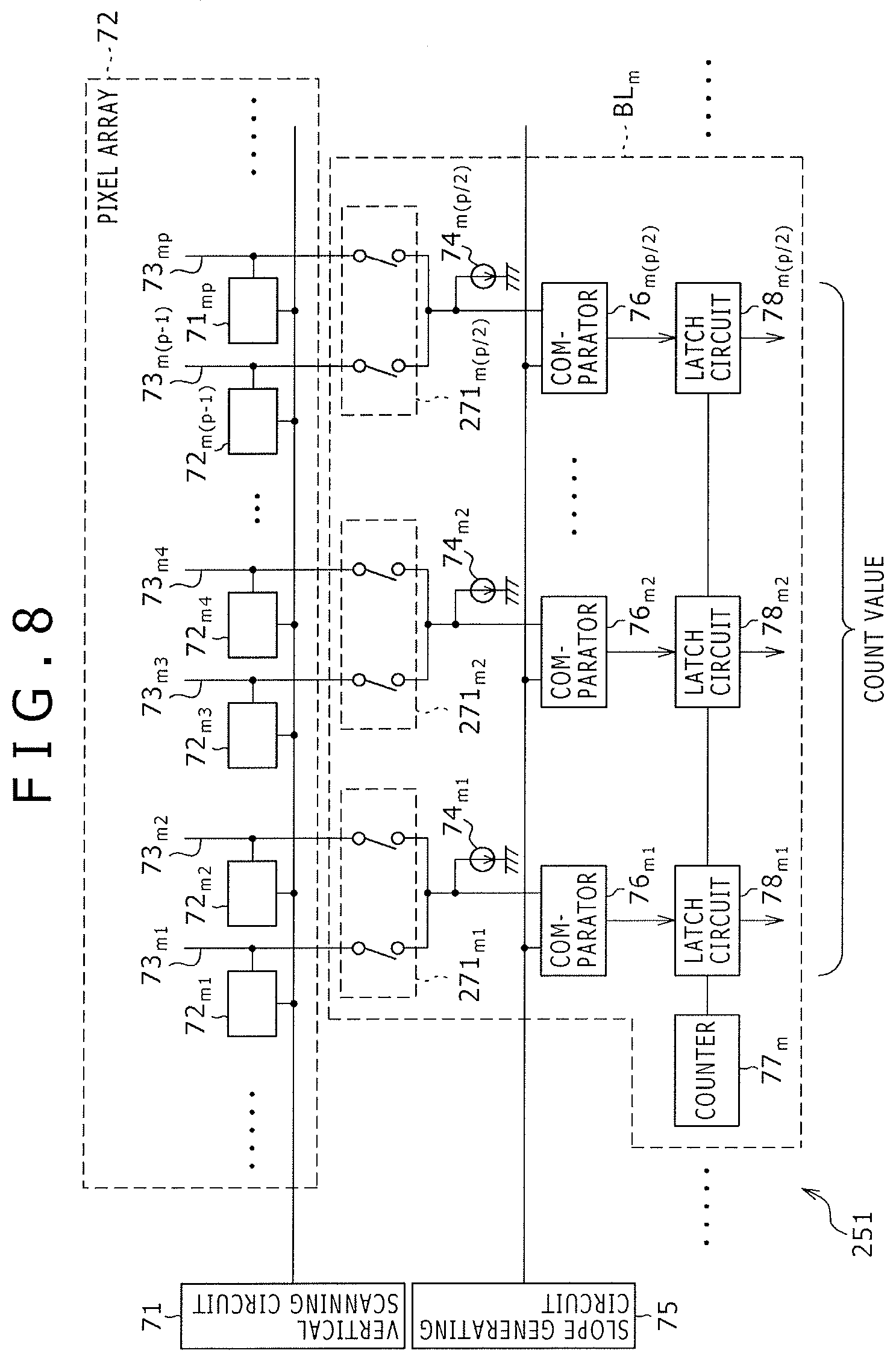
FIG. 8 is a block diagram showing a configuration example of still other embodiment of the solid-state image pickup device to which the present invention is applied.
In FIG. 8, the same references have been used as in FIG. 3 for similar components, and the description thereof is omitted.
A solid-state image pickup device 251 of FIG. 8 is identical to the solid-state image pickup device 51 of FIG. 3 in that circuit blocks BL.sub.m have counters 77.sub.m. The solid-state image pickup device 251 is different from the solid-state image pickup device 51 in that the circuit blocks BL.sub.m have P/2 pieces of current sources 74.sub.mp, comparators 76.sub.mp and latch circuits 78.sub.mp, and P/2 pieces of switches 271.sub.mp.
Under control of a controller (not shown), the switches 271.sub.mp selectively supply pixel signals supplied from vertical signal lines 73.sub.m(2p-1) and 73.sub.m(2p), to the comparators 76.sub.mp.
Thus, the solid-state image pickup device 251 has the configuration that a single comparator 76.sub.mp is shared between two pixels (two columns) 72.sub.m(2p-1) and 72.sub.m(2p).
Although in FIG. 8, a single comparator 76.sub.mp is shared between the two pixels (columns) 72.sub.m(2p-1) and 72.sub.m(2p) a single comparator 76.sub.mp may be shared among more than two pixels (columns) or n pixels (n columns).
Unlike the Patent Document 1 having P/2 arrangements that a single A/D converter (the comparator and the counter) is shared among n columns, the solid-state image pickup device 251 has the arrangement that a counter is shared among P/2 arrangements that a comparator and a latch circuit are shared among n columns. Therefore, the number of counters needed for n.times.(P/2) columns can be reduced from P/2 to one, permitting a reduction in power consumption.
As described above, the solid-state image pickup device 51, the solid-state image pickup device 151 and the solid-state image pickup device 251 are capable of reducing the number of the counters 77.sub.m, thereby reducing power consumption than the case of providing a counter for every column. That is, in each of the plurality of circuit blocks BL.sub.m, the plurality of comparators 76.sub.mp compare a pixel signal supplied through a vertical signal line connected to vertically aligned pixels 72.sub.mp among the plurality of pixels arranged in the matrix, and the slope signal whose voltage is changed at the constant slope from the predetermined initial voltage. In accordance with the comparison results of the comparators 76.sub.mp, the plurality of latch circuits 78.sub.mp store the count values obtained by the counters 77.sub.m, corresponding to an elapsed time from when the slope signal voltage is changed from the initial voltage to the voltage coinciding with the pixel signal.
Although the latch circuits 78.sub.mp store the count values in the embodiments described above, a sample-hold circuit or other storage media may store the count values.
Although there has been shown herein and described certain embodiments of the invention, it will be understood that many changes and modifications may be made therein without departing from the spirit or scope of the invention.
* * * * *
D00000
D00001
D00002
D00003
D00004
D00005
D00006
D00007
D00008
XML
uspto.report is an independent third-party trademark research tool that is not affiliated, endorsed, or sponsored by the United States Patent and Trademark Office (USPTO) or any other governmental organization. The information provided by uspto.report is based on publicly available data at the time of writing and is intended for informational purposes only.
While we strive to provide accurate and up-to-date information, we do not guarantee the accuracy, completeness, reliability, or suitability of the information displayed on this site. The use of this site is at your own risk. Any reliance you place on such information is therefore strictly at your own risk.
All official trademark data, including owner information, should be verified by visiting the official USPTO website at www.uspto.gov. This site is not intended to replace professional legal advice and should not be used as a substitute for consulting with a legal professional who is knowledgeable about trademark law.