Direct memory access data format
Hayes , et al. December 1, 2
U.S. patent number 10,853,285 [Application Number 16/267,163] was granted by the patent office on 2020-12-01 for direct memory access data format. This patent grant is currently assigned to Pure Storage, Inc.. The grantee listed for this patent is Pure Storage, Inc.. Invention is credited to John Davis, Brian Gold, Shantanu Gupta, John Hayes, Zhangxi Tan.


| United States Patent | 10,853,285 |
| Hayes , et al. | December 1, 2020 |
Direct memory access data format
Abstract
A method of applying a data format in a direct memory access transfer is provided. The method includes distributing user data throughout a plurality of storage nodes through erasure coding, wherein the plurality of storage nodes are housed within a single chassis that couples the storage nodes as a cluster, each of the plurality of storage nodes having nonvolatile solid-state memory for user data storage. The method includes reading a self-describing data portion from a first memory of the nonvolatile solid-state memory and extracting a destination from the self-describing data portion. The method includes writing data, from the self-describing data portion, to a second memory of the nonvolatile solid-state memory according to the destination.
| Inventors: | Hayes; John (Mountain View, CA), Gupta; Shantanu (Santa Clara, CA), Davis; John (San Francisco, CA), Gold; Brian (Los Altos, CA), Tan; Zhangxi (Mountain View, CA) | ||||||||||
|---|---|---|---|---|---|---|---|---|---|---|---|
| Applicant: |
|
||||||||||
| Assignee: | Pure Storage, Inc. (Mountain
View, CA) |
||||||||||
| Family ID: | 1000005215794 | ||||||||||
| Appl. No.: | 16/267,163 | ||||||||||
| Filed: | February 4, 2019 |
Prior Publication Data
| Document Identifier | Publication Date | |
|---|---|---|
| US 20190171594 A1 | Jun 6, 2019 | |
Related U.S. Patent Documents
| Application Number | Filing Date | Patent Number | Issue Date | ||
|---|---|---|---|---|---|
| 15686956 | Aug 25, 2017 | 10198380 | |||
| 14323894 | Aug 29, 2017 | 9747229 | |||
| Current U.S. Class: | 1/1 |
| Current CPC Class: | G06F 3/0688 (20130101); G06F 3/0656 (20130101); G06F 3/0625 (20130101); G06F 13/28 (20130101); G06F 3/0629 (20130101); G06F 3/0619 (20130101) |
| Current International Class: | G06F 13/36 (20060101); G06F 13/28 (20060101); G06F 3/06 (20060101) |
References Cited [Referenced By]
U.S. Patent Documents
| 5390327 | February 1995 | Lubbers et al. |
| 5479653 | December 1995 | Jones |
| 5649093 | July 1997 | Hanko et al. |
| 6275898 | August 2001 | DeKoning |
| 6535417 | March 2003 | Tsuda |
| 6643748 | November 2003 | Wieland |
| 6725392 | April 2004 | Frey et al. |
| 6836816 | December 2004 | Kendall |
| 6985995 | January 2006 | Holland et al. |
| 7032125 | April 2006 | Holt et al. |
| 7051155 | May 2006 | Talagala et al. |
| 7065617 | June 2006 | Wang |
| 7069383 | June 2006 | Yamamoto et al. |
| 7076606 | July 2006 | Orsley |
| 7107480 | September 2006 | Moshayedi et al. |
| 7159150 | January 2007 | Kenchammana-Hosekote et al. |
| 7162575 | January 2007 | Dalai et al. |
| 7164608 | January 2007 | Lee |
| 7334156 | February 2008 | Land et al. |
| 7370220 | May 2008 | Nguyen et al. |
| 7424498 | September 2008 | Patterson |
| 7424592 | September 2008 | Karr |
| 7444532 | October 2008 | Masuyama et al. |
| 7480658 | January 2009 | Heinle et al. |
| 7536506 | May 2009 | Ashmore et al. |
| 7558859 | July 2009 | Kasiolas |
| 7565446 | July 2009 | Talagala et al. |
| 7613947 | November 2009 | Coatney |
| 7681104 | March 2010 | Sim-Tang et al. |
| 7681105 | March 2010 | Sim-Tang et al. |
| 7730258 | June 2010 | Smith |
| 7743276 | June 2010 | Jacobsen et al. |
| 7757038 | July 2010 | Kitahara |
| 7778960 | August 2010 | Chatterjee et al. |
| 7814272 | October 2010 | Barrall et al. |
| 7814273 | October 2010 | Barrall |
| 7818531 | October 2010 | Barrall |
| 7827351 | November 2010 | Suetsugu et al. |
| 7827439 | November 2010 | Matthew et al. |
| 7870105 | January 2011 | Arakawa et al. |
| 7885938 | February 2011 | Greene et al. |
| 7886111 | February 2011 | Klemm et al. |
| 7908448 | March 2011 | Chatterjee et al. |
| 7916538 | March 2011 | Jeon et al. |
| 7941697 | May 2011 | Mathew et al. |
| 7958303 | June 2011 | Shuster |
| 7971129 | June 2011 | Watson |
| 7991822 | August 2011 | Bish et al. |
| 8010485 | August 2011 | Chatterjee et al. |
| 8010829 | August 2011 | Chatterjee et al. |
| 8020047 | September 2011 | Courtney |
| 8046548 | October 2011 | Chatterjee et al. |
| 8051361 | November 2011 | Sim-Tang et al. |
| 8051362 | November 2011 | Li et al. |
| 8082393 | December 2011 | Galloway et al. |
| 8086634 | December 2011 | Mimatsu |
| 8086911 | December 2011 | Taylor |
| 8090837 | January 2012 | Shin et al. |
| 8108502 | January 2012 | Tabbara et al. |
| 8117388 | February 2012 | Jernigan, IV |
| 8140821 | March 2012 | Raizen et al. |
| 8145838 | March 2012 | Miller et al. |
| 8145840 | March 2012 | Koul et al. |
| 8176360 | May 2012 | Frost et al. |
| 8180855 | May 2012 | Aiello et al. |
| 8200922 | June 2012 | McKean et al. |
| 8225006 | July 2012 | Karamcheti |
| 8239618 | August 2012 | Kotzur et al. |
| 8244999 | August 2012 | Chatterjee et al. |
| 8305811 | November 2012 | Jeon |
| 8315999 | November 2012 | Chatley et al. |
| 8327080 | December 2012 | Der |
| 8351290 | January 2013 | Huang et al. |
| 8375146 | February 2013 | Sinclair |
| 8397016 | March 2013 | Talagala et al. |
| 8402152 | March 2013 | Duran |
| 8412880 | April 2013 | Leibowitz et al. |
| 8423739 | April 2013 | Ash et al. |
| 8429436 | April 2013 | Filingim et al. |
| 8473778 | June 2013 | Simitci |
| 8479037 | July 2013 | Chatterjee et al. |
| 8498967 | July 2013 | Chatterjee et al. |
| 8522073 | August 2013 | Cohen |
| 8533527 | September 2013 | Daikokuya et al. |
| 8544029 | September 2013 | Bakke et al. |
| 8589625 | November 2013 | Colgrove et al. |
| 8595455 | November 2013 | Chatterjee et al. |
| 8615599 | December 2013 | Takefman et al. |
| 8627136 | January 2014 | Shankar et al. |
| 8627138 | January 2014 | Clark |
| 8660131 | February 2014 | Vermunt et al. |
| 8661218 | February 2014 | Piszczek et al. |
| 8700875 | April 2014 | Barron et al. |
| 8706694 | April 2014 | Chatterjee et al. |
| 8706914 | April 2014 | Duchesneau |
| 8713405 | April 2014 | Healey et al. |
| 8725730 | May 2014 | Keeton et al. |
| 8756387 | June 2014 | Frost et al. |
| 8762793 | June 2014 | Grube et al. |
| 8775858 | July 2014 | Gower et al. |
| 8775868 | July 2014 | Colgrove et al. |
| 8788913 | July 2014 | Xin et al. |
| 8799746 | August 2014 | Baker et al. |
| 8819311 | August 2014 | Liao |
| 8819383 | August 2014 | Jobanputra et al. |
| 8824261 | September 2014 | Miller et al. |
| 8843700 | September 2014 | Salessi et al. |
| 8850108 | September 2014 | Hayes et al. |
| 8850288 | September 2014 | Lazier et al. |
| 8856593 | October 2014 | Eckhardt et al. |
| 8856619 | October 2014 | Cypher |
| 8862847 | October 2014 | Feng et al. |
| 8862928 | October 2014 | Xavier et al. |
| 8868825 | October 2014 | Hayes |
| 8874836 | October 2014 | Hayes |
| 8886778 | November 2014 | Nedved et al. |
| 8898383 | November 2014 | Yamamoto et al. |
| 8898388 | November 2014 | Kimmel |
| 8904231 | December 2014 | Coatney et al. |
| 8918478 | December 2014 | Ozzie et al. |
| 8930307 | January 2015 | Colgrove et al. |
| 8930633 | January 2015 | Amit et al. |
| 8949502 | February 2015 | McKnight et al. |
| 8959110 | February 2015 | Smith et al. |
| 8977597 | March 2015 | Ganesh et al. |
| 9003144 | April 2015 | Hayes et al. |
| 9009724 | April 2015 | Gold et al. |
| 9021053 | April 2015 | Bernbo et al. |
| 9021215 | April 2015 | Meir et al. |
| 9025393 | May 2015 | Wu |
| 9043372 | May 2015 | Makkar et al. |
| 9053808 | June 2015 | Sprouse |
| 9058155 | June 2015 | Cepulis et al. |
| 9116819 | August 2015 | Cope et al. |
| 9117536 | August 2015 | Yoon |
| 9122401 | September 2015 | Zaltsman et al. |
| 9134908 | September 2015 | Horn et al. |
| 9153337 | October 2015 | Sutardja |
| 9189650 | November 2015 | Jaye et al. |
| 9201733 | December 2015 | Verma |
| 9207876 | December 2015 | Shu et al. |
| 9251066 | February 2016 | Colgrove et al. |
| 9323667 | April 2016 | Bennett |
| 9323681 | April 2016 | Apostolides et al. |
| 9348538 | May 2016 | Mallaiah et al. |
| 9384082 | July 2016 | Lee et al. |
| 9390019 | July 2016 | Patterson et al. |
| 9405478 | August 2016 | Koseki et al. |
| 9432541 | August 2016 | Ishida |
| 9477632 | October 2016 | Du |
| 9552299 | January 2017 | Stelzer |
| 9747229 | August 2017 | Hayes |
| 9818478 | November 2017 | Chung |
| 9829066 | November 2017 | Thomas et al. |
| 10198380 | February 2019 | Hayes |
| 2002/0144059 | October 2002 | Kendall |
| 2003/0105984 | June 2003 | Masuyama et al. |
| 2003/0110205 | June 2003 | Johnson |
| 2004/0161086 | August 2004 | Buntin et al. |
| 2005/0001652 | January 2005 | Malik et al. |
| 2005/0076228 | April 2005 | Davis et al. |
| 2005/0235132 | October 2005 | Karr et al. |
| 2005/0278460 | December 2005 | Shin et al. |
| 2005/0283649 | December 2005 | Turner et al. |
| 2006/0015683 | January 2006 | Ashmore et al. |
| 2006/0114930 | June 2006 | Lucas et al. |
| 2006/0174157 | August 2006 | Barrall et al. |
| 2006/0248294 | November 2006 | Nedved et al. |
| 2007/0079068 | April 2007 | Draggon |
| 2007/0214194 | September 2007 | Reuter |
| 2007/0214314 | September 2007 | Reuter |
| 2007/0234016 | October 2007 | Davis et al. |
| 2007/0268905 | November 2007 | Baker et al. |
| 2008/0080709 | April 2008 | Michtchenko et al. |
| 2008/0107274 | May 2008 | Worthy |
| 2008/0155191 | June 2008 | Anderson et al. |
| 2008/0295118 | November 2008 | Liao |
| 2009/0077208 | March 2009 | Nguyen et al. |
| 2009/0138654 | May 2009 | Sutardja |
| 2009/0216910 | August 2009 | Duchesneau |
| 2009/0216920 | August 2009 | Lauterbach et al. |
| 2010/0017444 | January 2010 | Chatterjee et al. |
| 2010/0042636 | February 2010 | Lu |
| 2010/0094806 | April 2010 | Apostolides et al. |
| 2010/0115070 | May 2010 | Missimilly |
| 2010/0125695 | May 2010 | Wu et al. |
| 2010/0162076 | June 2010 | Sim-Tang et al. |
| 2010/0169707 | July 2010 | Mathew et al. |
| 2010/0174576 | July 2010 | Naylor |
| 2010/0268908 | October 2010 | Ouyang et al. |
| 2011/0040925 | February 2011 | Frost et al. |
| 2011/0060927 | March 2011 | Fillingim et al. |
| 2011/0119462 | May 2011 | Leach et al. |
| 2011/0219170 | September 2011 | Frost et al. |
| 2011/0238625 | September 2011 | Hamaguchi et al. |
| 2011/0264843 | October 2011 | Haines et al. |
| 2011/0302369 | December 2011 | Goto et al. |
| 2012/0011398 | January 2012 | Eckhardt |
| 2012/0079318 | March 2012 | Colgrove et al. |
| 2012/0110249 | May 2012 | Jeong et al. |
| 2012/0131253 | May 2012 | McKnight et al. |
| 2012/0158923 | June 2012 | Mohamed et al. |
| 2012/0191900 | July 2012 | Kunimatsu et al. |
| 2012/0198152 | August 2012 | Terry et al. |
| 2012/0198261 | August 2012 | Brown et al. |
| 2012/0209943 | August 2012 | Jung |
| 2012/0226934 | September 2012 | Rao |
| 2012/0246435 | September 2012 | Meir et al. |
| 2012/0260055 | October 2012 | Murase |
| 2012/0311557 | December 2012 | Resch |
| 2013/0022201 | January 2013 | Glew et al. |
| 2013/0036314 | February 2013 | Glew et al. |
| 2013/0042056 | February 2013 | Shats et al. |
| 2013/0060884 | March 2013 | Bernbo et al. |
| 2013/0067188 | March 2013 | Mehra et al. |
| 2013/0073894 | March 2013 | Xavier et al. |
| 2013/0124776 | May 2013 | Hallak et al. |
| 2013/0132800 | May 2013 | Healy et al. |
| 2013/0151653 | June 2013 | Sawiki |
| 2013/0151771 | June 2013 | Tsukahara et al. |
| 2013/0173853 | July 2013 | Ungureanu et al. |
| 2013/0238554 | September 2013 | Yucel et al. |
| 2013/0339314 | December 2013 | Carpentier et al. |
| 2013/0339635 | December 2013 | Amit et al. |
| 2013/0339818 | December 2013 | Baker et al. |
| 2014/0040535 | February 2014 | Lee |
| 2014/0040702 | February 2014 | He et al. |
| 2014/0047263 | February 2014 | Coatney et al. |
| 2014/0047269 | February 2014 | Kim |
| 2014/0063721 | March 2014 | Herman et al. |
| 2014/0064048 | March 2014 | Cohen et al. |
| 2014/0068224 | March 2014 | Fan et al. |
| 2014/0075252 | March 2014 | Luo et al. |
| 2014/0136880 | May 2014 | Shankar et al. |
| 2014/0181402 | June 2014 | White |
| 2014/0237164 | August 2014 | Le et al. |
| 2014/0279936 | September 2014 | Bernbo et al. |
| 2014/0280025 | September 2014 | Eidson et al. |
| 2014/0289588 | September 2014 | Nagadomi et al. |
| 2014/0380125 | December 2014 | Calder et al. |
| 2014/0380126 | December 2014 | Yekhanin et al. |
| 2015/0032720 | January 2015 | James |
| 2015/0039645 | February 2015 | Lewis |
| 2015/0039849 | February 2015 | Lewis |
| 2015/0089283 | March 2015 | Kermarrec et al. |
| 2015/0100746 | April 2015 | Rychlik |
| 2015/0134824 | May 2015 | Mickens |
| 2015/0153800 | June 2015 | Lucas et al. |
| 2015/0180714 | June 2015 | Chunn |
| 2015/0280959 | October 2015 | Vincent |
| 2164006 | Mar 2010 | EP | |||
| 2256621 | Dec 2010 | EP | |||
| WO 02-13033 | Feb 2002 | WO | |||
| WO 2008103569 | Aug 2008 | WO | |||
| WO 2008157081 | Dec 2008 | WO | |||
| WO 2013032825 | Jul 2013 | WO | |||
Other References
|
Hwang, Kai, et al. "RAID-x: A New Distributed Disk Array for I/O-Centric Cluster Computing," HPDC '00 Proceedings of the 9th IEEE International Symposium on High Performance Distributed Computing, IEEE, 2000, pp. 279-286. cited by applicant . Schmid, Patrick: "RAID Scaling Charts, Part 3:4-128 kB Stripes Compared", Tom's Hardware, Nov. 27, 2007 (http://www.tomshardware.com/reviews/RAID-SCALING-CHARTS.1735-4.html), See pp. 1-2. cited by applicant . Storer, Mark W. et al., "Pergamum: Replacing Tape with Energy Efficient, Reliable, Disk-Based Archival Storage," Fast '08: 6th USENIX Conference on File and Storage Technologies, San Jose, CA, Feb. 26-29, 2008 pp. 1-16. cited by applicant . Ju-Kyeong Kim et al., "Data Access Frequency based Data Replication Method using Erasure Codes in Cloud Storage System", Journal of the Institute of Electronics and Information Engineers, Feb. 2014, vol. 51, No. 2, pp. 85-91. cited by applicant . International Search Report and the Written Opinion of the International Searching Authority, PCT/US2015/018169, dated May 15, 2015. cited by applicant . International Search Report and the Written Opinion of the International Searching Authority, PCT/US2015/034302, dated Sep. 11, 2015. cited by applicant . International Search Report and the Written Opinion of the International Searching Authority, PCT/US2015/039135, dated Sep. 18, 2015. cited by applicant . International Search Report and the Written Opinion of the International Searching Authority, PCT/US2015/039136, dated Sep. 23, 2015. cited by applicant . International Search Report, PCT/US2015/039142, dated Sep. 24, 2015. cited by applicant . International Search Report, PCT/US2015/034291, dated Sep. 30, 2015. cited by applicant . International Search Report and the Written Opinion of the International Searching Authority, PCT/US2015/039137, dated Oct. 1, 2015. cited by applicant . International Search Report, PCT/US2015/044370, dated Dec. 15, 2015. cited by applicant . International Search Report amd the Written Opinion of the International Searching Authority, PCT/US2016/031039, dated May 5, 2016. cited by applicant . International Search Report, PCT/US2016/014604, dated May 19, 2016. cited by applicant . International Search Report, PCT/US2016/014361, dated May 30, 2016. cited by applicant . International Search Report, PCT/US2016/014356, dated Jun. 28, 2016. cited by applicant . International Search Report, PCT/US2016/014357, dated Jun. 29, 2016. cited by applicant . International Seach Report and the Written Opinion of the International Searching Authority, PCT/US2016/016504, dated Jul. 6, 2016. cited by applicant . International Seach Report and the Written Opinion of the International Searching Authority, PCT/US2016/024391, dated Jul. 12, 2016. cited by applicant . International Seach Report and the Written Opinion of the International Searching Authority, PCT/US2016/026529, dated Jul. 19, 2016. cited by applicant . International Seach Report and the Written Opinion of the International Searching Authority, PCT/US2016/023485, dated Jul. 21, 2016. cited by applicant . International Seach Report and the Written Opinion of the International Searching Authority, PCT/US2016/033306, dated Aug. 19, 2016. cited by applicant . International Seach Report and the Written Opinion of the International Searching Authority, PCT/US2016/047808, dated Nov. 25, 2016. cited by applicant . Stalzer, Mark A., "Flash Blades: System Architecture and Applications," Proceedings of the 2nd Workshop on Architectures and Systems for Big Data, Association for Computing Machinery, New York, NY, 2012, pp. 10-14. cited by applicant . International Seach Report and the Written Opinion of the International Searching Authority, PCT/US2016/042147, dated Nov. 30, 2016. cited by applicant. |
Primary Examiner: Phan; Raymond N
Attorney, Agent or Firm: Womble Bond Dickinson (US) LLP
Claims
What is claimed is:
1. A method, comprising: receiving data; segmenting the received data; storing the segmented data into a first memory, each of the stored segmented data includes destination information and status information; and transferring the segmented data from the first memory to a second memory based on a location extracted from the destination information and conditioned on the status information.
2. The method of claim 1, further comprising: confirming the transferring of the data to the second memory by updating the status information.
3. The method of claim 1, further comprising: writing an identifier of the segmented data to a header of a non-volatile memory page, wherein the second memory includes non-volatile memory having the non-volatile memory page containing the location.
4. The method of claim 1, further comprising: extracting the status information responsive to a loss of power, and wherein the transferring is responsive to the loss of power and responsive to the status information indicating the segmented data has not yet been written to the second memory.
5. The method of claim 1, further comprising: determining whether the data has been written to the second memory based on the status information.
6. The method of claim 1, further comprising: assigning sequential non-repeating addresses over multiple address spaces that map each segmented data to an inode.
7. The method of claim 1, further comprising: writing an indication that the segmented data will not be used and need not be transferred to the second memory to the status information in the first memory.
8. A method of moving data by direct memory access (DMA), comprising: accessing, through a direct memory access (DMA unit, a data segment from a first memory, the data segment including destination information regarding a destination of the data segment, and a status information associated with transfer of the data segment from the first memory to a second memory; and writing, through the DMA unit, the data segment to the destination in the second memory according to the destination information as conditioned on the status information.
9. The method of claim 8, further comprising: writing, using the DMA unit, to the status information of the first memory an indication of successful data transfer, responsive to writing the data segment to the destination in the second memory.
10. The method of claim 8, wherein the destination information includes one of an address, a destination pointer, or an offset.
11. The method of claim 8, further comprising: writing an identifier to a header of a non-volatile memory page, wherein the identifier identifies the data as to an inode identifier (ID), a medium address, or a segment ID, and wherein the non-volatile memory page is in the second memory.
12. The method of claim 8, further comprising: determining from the status information that the data has not been written to the second memory, wherein the writing the data segment to the destination in the second memory is responsive to the determining.
13. The method of claim 8, further comprising: determining from status information that the data segment has been written to the second memory; writing, using the DMA unit, further data from the first memory to the second memory, responsive to a power loss, without rewriting the data that has been written to the second memory according to the status information.
14. The method of claim 8, wherein the first memory includes non-volatile random-access memory (NVRAM) and the second memory includes non-volatile memory.
15. A storage cluster, comprising: a first memory, configured to hold a plurality of data segments, each data segment including destination information for the data segment, and status information about transfer of the data segment from the first memory to a second memory of the storage cluster; a direct memory access (DMA) unit, configured to perform actions including: identifying a destination for one of the plurality of data segments from the destination information in the first memory; and writing the data segment, conditioned upon the status information, to the destination in the second memory.
16. The storage cluster of claim 15, further comprising: the first memory includes non-volatile random access memory (NVRAM).
17. The storage cluster of claim 15, further comprising: the second memory includes non-volatile memory; and an energy reserve coupled to the first memory, the second memory and the DMA unit, the energy reserve configured to provide sufficient power for the DMA unit to transfer contents of the first memory to the second memory responsive to a power loss.
18. The storage cluster of claim 15, further comprising: assigning sequential non-repeating addresses over multiple address spaces that map the data segment to an inode.
19. The storage cluster of claim 15, wherein: the actions further include updating to the status information to confirm transfer of the data segment from the first memory to the second memory, responsive to writing the data segment to the destination in the second memory.
20. The storage cluster of claim 15, further comprising: the one of the plurality of data segments in the first memory includes a status of the data segment indicating one of whether the data of the one of the plurality of data segments has been written to the second memory or whether the data of the one of the plurality of data segments will be used.
Description
BACKGROUND
Solid-state memory, such as flash, is currently in use in solid-state drives (SSD) to augment or replace conventional hard disk drives (HDD), writable CD (compact disk) or writable DVD (digital versatile disk) drives, collectively known as spinning media, and tape drives, for storage of large amounts of data. Flash and other solid-state memories have characteristics that differ from spinning media. Yet, many solid-state drives are designed to conform to hard disk drive standards for compatibility reasons, which makes it difficult to provide enhanced features or take advantage of unique aspects of flash and other solid-state memory. Data formats conforming to hard disk drive standards may be suboptimal when applied to solid-state memory.
It is within this context that the embodiments arise.
SUMMARY
In some embodiments, a method of applying a data format in a direct memory access transfer is provided. The method includes distributing user data throughout a plurality of storage nodes through erasure coding, wherein the plurality of storage nodes are housed within a single chassis that couples the storage nodes as a cluster, each of the plurality of storage nodes having nonvolatile solid-state memory for user data storage. The method includes reading a self-describing data portion from a first memory of the nonvolatile solid-state memory and extracting a destination from the self-describing data portion. The method includes writing data, from the self-describing data portion, to a second memory of the nonvolatile solid-state memory according to the destination, wherein at least one method operation is performed by a processor.
Other aspects and advantages of the embodiments will become apparent from the following detailed description taken in conjunction with the accompanying drawings which illustrate, by way of example, the principles of the described embodiments.
BRIEF DESCRIPTION OF THE DRAWINGS
The described embodiments and the advantages thereof may best be understood by reference to the following description taken in conjunction with the accompanying drawings. These drawings in no way limit any changes in form and detail that may be made to the described embodiments by one skilled in the art without departing from the spirit and scope of the described embodiments.
FIG. 1 is a perspective view of a storage cluster with multiple storage nodes and internal storage coupled to each storage node to provide network attached storage, in accordance with some embodiments.
FIG. 2 is a system diagram of an enterprise computing system, which can use one or more of the storage clusters of FIG. 1 as a storage resource in some embodiments.
FIG. 3 is a multiple level block diagram, showing contents of a storage node and contents of one of the non-volatile solid-state storages in accordance with some embodiments.
FIG. 4 is a block diagram showing a communication path for redundant copies of metadata, with further details of storage nodes and solid-state storages in accordance with some embodiments.
FIG. 5 is an address and data diagram showing address translation as applied to user data being stored in some embodiments.
FIG. 6 is a block diagram showing a DMA unit transferring data that has a self-describing data format, in in some embodiments.
FIG. 7 is a flow diagram of a method for applying a self-describing data format to a direct memory access transfer in some embodiments.
FIG. 8 is an illustration showing an exemplary computing device which may implement the embodiments described herein.
DETAILED DESCRIPTION
The embodiments below describe a storage cluster that stores user data, such as user data originating from one or more user or client systems or other sources external to the storage cluster. The storage cluster distributes user data across storage nodes housed within a chassis, using erasure coding and redundant copies of metadata. Erasure coding refers to a method of data protection in which data is broken into fragments, expanded and encoded with redundant data pieces and stored across a set of different locations, such as disks, storage nodes or geographic locations. Flash memory is one type of solid-state memory that may be integrated with the embodiments, although the embodiments may be extended to other types of solid-state memory or other storage medium, including non-solid state memory. Control of storage locations and workloads are distributed across the storage locations in a clustered peer-to-peer system. Tasks such as mediating communications between the various storage nodes, detecting when a storage node has become unavailable, and balancing I/Os (inputs and outputs) across the various storage nodes, are all handled on a distributed basis. Data is laid out or distributed across multiple storage nodes in data fragments or stripes that support data recovery in some embodiments. Ownership of data can be reassigned within a cluster, independent of input and output patterns. This architecture described in more detail below allows a storage node in the cluster to fail, with the system remaining operational, since the data can be reconstructed from other storage nodes and thus remain available for input and output operations. In various embodiments, a storage node may be referred to as a cluster node, a blade, or a server.
The storage cluster is contained within a chassis, i.e., an enclosure housing one or more storage nodes. A mechanism to provide power to each storage node, such as a power distribution bus, and a communication mechanism, such as a communication bus that enables communication between the storage nodes are included within the chassis. The storage cluster can run as an independent system in one location according to some embodiments. In one embodiment, a chassis contains at least two instances of the power distribution and the internal and external communication bus which may be enabled or disabled independently. The internal communication bus may be an Ethernet bus, however, other technologies such as Peripheral Component Interconnect (PCI) Express, InfiniBand, and others, are equally suitable. The chassis provides a port for an external communication bus for enabling communication between multiple chassis, directly or through a switch, and with client systems. The external communication may use a technology such as Ethernet, InfiniBand, Fibre Channel, etc. In some embodiments, the external communication bus uses different communication bus technologies for inter-chassis and client communication. If a switch is deployed within or between chassis, the switch may act as a translation between multiple protocols or technologies. When multiple chassis are connected to define a storage cluster, the storage cluster may be accessed by a client using either proprietary interfaces or standard interfaces such as network file system (NFS), common internet file system (CIFS), small computer system interface (SCSI) or hypertext transfer protocol (HTTP). Translation from the client protocol may occur at the switch, chassis external communication bus or within each storage node.
Each storage node may be one or more storage servers and each storage server is connected to one or more non-volatile solid state memory units, which may be referred to as storage units. One embodiment includes a single storage server in each storage node and between one to eight non-volatile solid state memory units, however this one example is not meant to be limiting. The storage server may include a processor, dynamic random access memory (DRAM) and interfaces for the internal communication bus and power distribution for each of the power buses. Inside the storage node, the interfaces and storage unit share a communication bus, e.g., PCI Express, in some embodiments. The non-volatile solid state memory units may directly access the internal communication bus interface through a storage node communication bus, or request the storage node to access the bus interface. The non-volatile solid state memory unit contains an embedded central processing unit (CPU), solid state storage controller, and a quantity of solid state mass storage, e.g., between 2-32 terabytes (TB) in some embodiments. An embedded volatile storage medium, such as DRAM, and an energy reserve apparatus are included in the non-volatile solid state memory unit. In some embodiments, the energy reserve apparatus is a capacitor, super-capacitor, or battery that enables transferring a subset of DRAM contents to a stable storage medium in the case of power loss. In some embodiments, the non-volatile solid state memory unit is constructed with a storage class memory, such as phase change or other resistive random access memory (RRAM) or magnetoresistive random access memory (MRAM) that substitutes for DRAM and enables a reduced power hold-up apparatus.
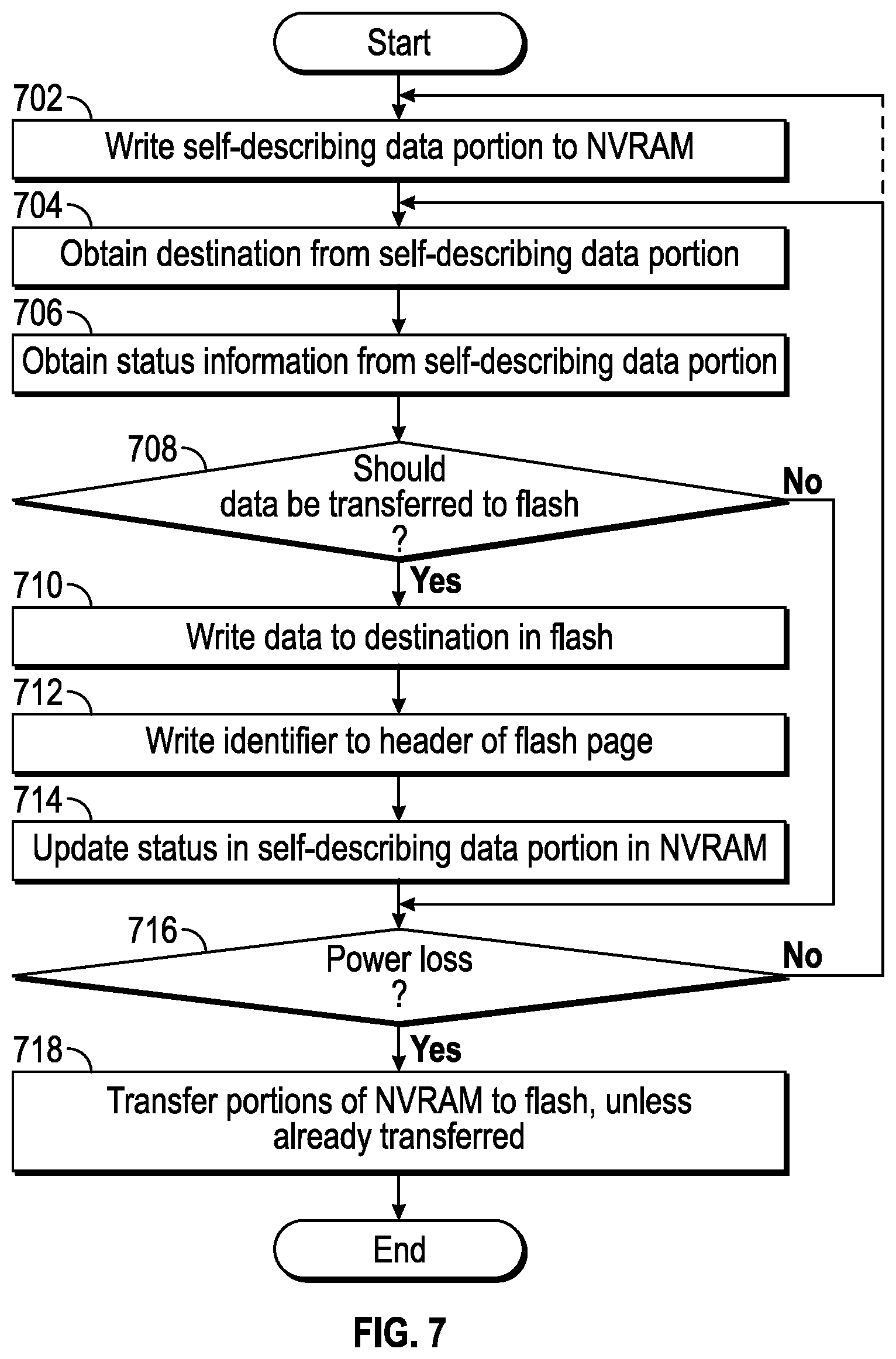
The storage nodes have one or more non-volatile solid-state storage units, each of which has non-volatile random-access memory (NVRAM) and flash memory, in some embodiments. The non-volatile solid-state storage units apply various address spaces for storing user data. Data is written to NVRAM to await transfer to flash memory, and this data has a self-describing format. Self-describing data portions written to NVRAM have a status section, a destination section, and the data. In each non-volatile solid-state storage unit a direct memory access (DMA) unit determines the destination for the data in the NVRAM, and writes the data to the flash memory accordingly. This operation is conditioned on the status from the status section, which the DMA updates to confirm the write to flash. The DMA unit also writes an identifier to the header of the flash page on which the data is written. Applying this self-describing data format to DMA transfers enhances overall data throughput and efficiency.
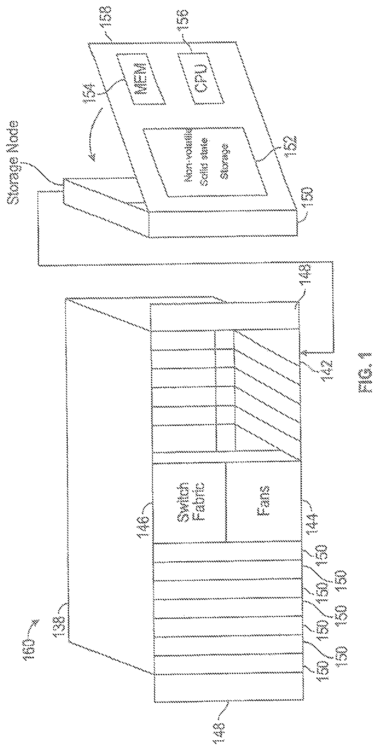
FIG. 1 is a perspective view of a storage cluster 160, with multiple storage nodes 150 and internal solid-state memory coupled to each storage node to provide network attached storage or storage area network, in accordance with some embodiments. A network attached storage, storage area network, or a storage cluster, or other storage memory, could include one or more storage clusters 160, each having one or more storage nodes 150, in a flexible and reconfigurable arrangement of both the physical components and the amount of storage memory provided thereby. The storage cluster 160 is designed to fit in a rack, and one or more racks can be set up and populated as desired for the storage memory. The storage cluster 160 has a single chassis 138 having multiple slots 142. It should be appreciated that chassis 138 may be referred to as a housing, enclosure, or rack unit. In one embodiment, the chassis 138 has fourteen slots 142, although other numbers of slots are readily devised. For example, some embodiments have four slots, eight slots, sixteen slots, thirty-two slots, or other suitable number of slots. Each slot 142 can accommodate one storage node 150 in some embodiments. Chassis 138 includes flaps 148 that can be utilized to mount the chassis 138 on a rack. Fans 144 provide air circulation for cooling of the storage nodes 150 and components thereof, although other cooling components could be used, or an embodiment could be devised without cooling components. A switch fabric 146 couples storage nodes 150 within chassis 138 together and to a network for communication to the memory. In an embodiment depicted in FIG. 1, the slots 142 to the left of the switch fabric 146 and fans 144 are shown occupied by storage nodes 150, while the slots 142 to the right of the switch fabric 146 and fans 144 are empty and available for insertion of storage node 150 for illustrative purposes. This configuration is one example, and one or more storage nodes 150 could occupy the slots 142 in various further arrangements. The storage node arrangements need not be sequential or adjacent in some embodiments. Storage nodes 150 are hot pluggable, meaning that a storage node 150 can be inserted into a slot 142 in the chassis 138, or removed from a slot 142, without stopping or powering down the system. Upon insertion or removal of storage node 150 from slot 142, the system automatically reconfigures in order to recognize and adapt to the change. Reconfiguration, in some embodiments, includes restoring redundancy and/or rebalancing data or load.
Each storage node 150 can have multiple components. In the embodiment shown here, the storage node 150 includes a printed circuit board 158 populated by a CPU 156, i.e., processor, a memory 154 coupled to the CPU 156, and a non-volatile solid state storage 152 coupled to the CPU 156, although other mountings and/or components could be used in further embodiments. The memory 154 has instructions which are executed by the CPU 156 and/or data operated on by the CPU 156. As further explained below, the non-volatile solid state storage 152 includes flash or, in further embodiments, other types of solid-state memory.
Storage cluster 160 is scalable, meaning that storage capacity with non-uniform storage sizes is readily added, as described above. One or more storage nodes 150 can be plugged into or removed from each chassis and the storage cluster self-configures in some embodiments. Plug-in storage nodes 150, whether installed in a chassis as delivered or later added, can have different sizes. For example, in one embodiment a storage node 150 can have any multiple of 4 TB, e.g., 8 TB, 12 TB, 16 TB, 32 TB, etc. In further embodiments, a storage node 150 could have any multiple of other storage amounts or capacities. Storage capacity of each storage node 150 is broadcast, and influences decisions of how to stripe the data. For maximum storage efficiency, an embodiment can self-configure as wide as possible in the stripe, subject to a predetermined requirement of continued operation with loss of up to one, or up to two, non-volatile solid state storage units 152 or storage nodes 150 within the chassis.
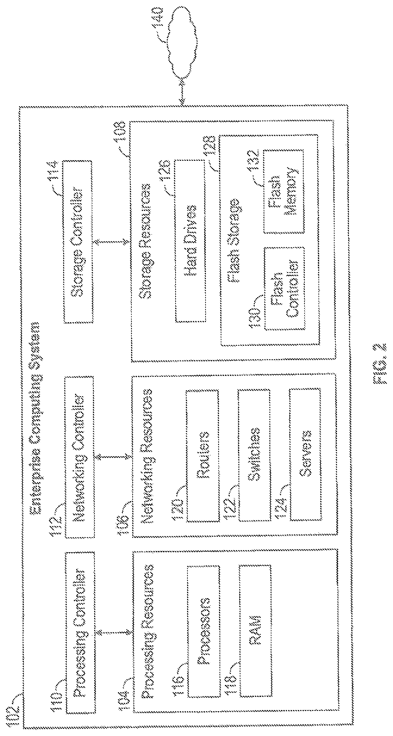
FIG. 2 is a system diagram of an enterprise computing system 102, which can use one or more of the storage nodes, storage clusters and/or non-volatile solid-state storage of FIG. 1 as a storage resource 108. For example, flash storage 128 of FIG. 2 may integrate the storage nodes, storage clusters and/or non-volatile solid-state storage of FIG. 1 in some embodiments. The enterprise computing system 102 has processing resources 104, networking resources 106 and storage resources 108, including flash storage 128. A flash controller 130 and flash memory 132 are included in the flash storage 128. In various embodiments, the flash storage 128 could include one or more storage nodes or storage clusters, with the flash controller 130 including the CPUs, and the flash memory 132 including the non-volatile solid-state storage of the storage nodes. In some embodiments flash memory 132 may include different types of flash memory or the same type of flash memory. The enterprise computing system 102 illustrates an environment suitable for deployment of the flash storage 128, although the flash storage 128 could be used in other computing systems or devices, larger or smaller, or in variations of the enterprise computing system 102, with fewer or additional resources. The enterprise computing system 102 can be coupled to a network 140, such as the Internet, in order to provide or make use of services. For example, the enterprise computing system 102 could provide cloud services, physical computing resources, or virtual computing services.
In the enterprise computing system 102, various resources are arranged and managed by various controllers. A processing controller 110 manages the processing resources 104, which include processors 116 and random-access memory (RAM) 118. Networking controller 112 manages the networking resources 106, which include routers 120, switches 122, and servers 124. A storage controller 114 manages storage resources 108, which include hard drives 126 and flash storage 128. Other types of processing resources, networking resources, and storage resources could be included with the embodiments. In some embodiments, the flash storage 128 completely replaces the hard drives 126. The enterprise computing system 102 can provide or allocate the various resources as physical computing resources, or in variations, as virtual computing resources supported by physical computing resources. For example, the various resources could be implemented using one or more servers executing software. Files or data objects, or other forms of data, are stored in the storage resources 108.
In various embodiments, an enterprise computing system 102 could include multiple racks populated by storage clusters, and these could be located in a single physical location such as in a cluster or a server farm. In other embodiments the multiple racks could be located at multiple physical locations such as in various cities, states or countries, connected by a network. Each of the racks, each of the storage clusters, each of the storage nodes, and each of the non-volatile solid-state storage could be individually configured with a respective amount of storage space, which is then reconfigurable independently of the others. Storage capacity can thus be flexibly added, upgraded, subtracted, recovered and/or reconfigured at each of the non-volatile solid-state storages. As mentioned previously, each storage node could implement one or more servers in some embodiments.
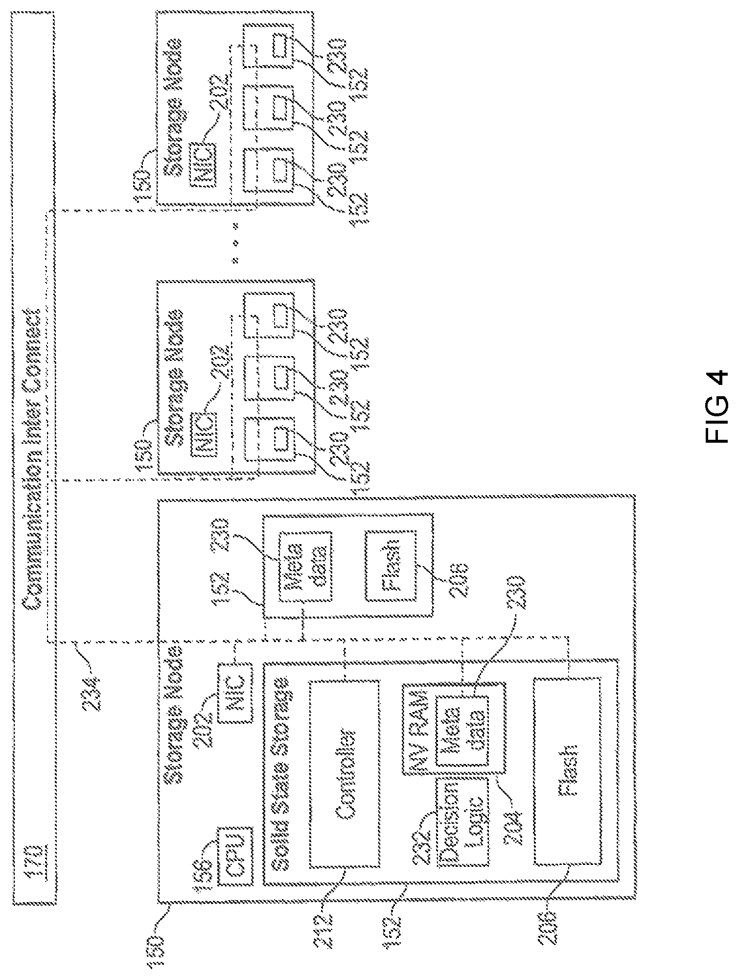
FIG. 3 is a multiple level block diagram, showing contents of a storage node 150 and contents of a non-volatile solid state storage 152 of the storage node 150. Data is communicated to and from the storage node 150 by a network interface controller (NIC) 202 in some embodiments. Each storage node 150 has a CPU 156, and one or more non-volatile solid state storage 152, as discussed above. Moving down one level in FIG. 3, each non-volatile solid state storage 152 has a relatively fast non-volatile solid state memory, such as nonvolatile random access memory (NVRAM) 204, and flash memory 206. In some embodiments, NVRAM 204 may be a component that does not require program/erase cycles (DRAM, MRAM, PCM), and can be a memory that can support being written vastly more often than the memory is read from. Moving down another level in FIG. 3, the NVRAM 204 is implemented in one embodiment as high speed volatile memory, such as dynamic random access memory (DRAM) 216, backed up by energy reserve 218. Energy reserve 218 provides sufficient electrical power to keep the DRAM 216 powered long enough for contents to be transferred to the flash memory 206 in the event of power failure. In some embodiments, energy reserve 218 is a capacitor, super-capacitor, battery, or other device, that supplies a suitable supply of energy sufficient to enable the transfer of the contents of DRAM 216 to a stable storage medium in the case of power loss. The flash memory 206 is implemented as multiple flash dies 222, which may be referred to as packages of flash dies 222 or an array of flash dies 222. It should be appreciated that the flash dies 222 could be packaged in any number of ways, with a single die per package, multiple dies per package (i.e. multichip packages), in hybrid packages, as bare dies on a printed circuit board or other substrate, as encapsulated dies, etc. In the embodiment shown, the non-volatile solid state storage 152 has a controller 212 or other processor, and an input output (I/O) port 210 coupled to the controller 212. I/O port 210 is coupled to the CPU 156 and/or the network interface controller 202 of the flash storage node 150. Flash input output (I/O) port 220 is coupled to the flash dies 222, and a direct memory access unit (DMA) 214 is coupled to the controller 212, the DRAM 216 and the flash dies 222. In the embodiment shown, the I/O port 210, controller 212, DMA unit 214 and flash I/O port 220 are implemented on a programmable logic device (PLD) 208, e.g., a field programmable gate array (FPGA). In this embodiment, each flash die 222 has pages, organized as sixteen kB (kilobyte) pages 224, and a register 226 through which data can be written to or read from the flash die 222. In further embodiments, other types of solid-state memory are used in place of, or in addition to flash memory illustrated within flash die 222.
In NVRAM 204, redundancy is not organized by segments but instead by messages, where each message (128 bytes to 128 kB) establishes its own data stripe, in some embodiments. NVRAM is maintained at the same redundancy as segment storage and operates within the same storage node groups in some embodiments. Because messages are stored individually the stripe width is determined both by message size and the storage cluster configuration. Larger messages may be more efficiently stored as wider strips.
Two of the many tasks of the CPU 156 on a storage node 150 are to break up write data, and reassemble read data. When the system has determined that data is to be written, an authority for that data is located in one of the non-volatile solid-state storages 152. The authority may be embodied as metadata, including one or more lists such as lists of data segments which the nonvolatile solid-state storage 152 manages. When a segment ID for data is already determined the request to write is forwarded to the non-volatile solid-state storage 152 currently determined to be the host of the authority determined from the segment. The host CPU 156 of the storage node 150, on which the non-volatile solid-state storage 152 and corresponding authority reside, then breaks up or shards the data and transmits the data out to various non-volatile solid-state storage 152. The transmitted data is written as a data stripe in accordance with an erasure coding scheme. In some embodiments, data is requested to be pulled, and in other embodiments, data is pushed. In reverse, when data is read, the authority for the segment ID containing the data is located as described above. The host CPU 156 of the storage node 150 on which the non-volatile solid-state storage 152 and corresponding authority reside requests the data from the non-volatile solid-state storage and corresponding storage nodes pointed to by the authority. In some embodiments the data is read from flash storage as a data stripe. The host CPU 156 of storage node 150 then reassembles the read data, correcting any errors (if present) according to the appropriate erasure coding scheme, and forwards the reassembled data to the network. In further embodiments, some or all of these tasks can be handled in the non-volatile solid-state storage 152. In some embodiments, the segment host requests the data be sent to storage node 150 by requesting pages from storage and then sending the data to the storage node making the original request.
In some systems, for example in UNIX-style file systems, data is handled with an index node or inode, which specifies a data structure that represents an object in a file system. The object could be a file or a directory, for example. Metadata may accompany the object, as attributes such as permission data and a creation timestamp, among other attributes. A segment number could be assigned to all or a portion of such an object in a file system. In other systems, data segments are handled with a segment number assigned elsewhere. For purposes of discussion, the unit of distribution is an entity, and an entity can be a file, a directory or a segment. That is, entities are units of data or metadata stored by a storage system. Entities are grouped into sets called authorities. Each authority has an authority owner, which is a storage node that has the exclusive right to update the entities in the authority. In other words, a storage node contains the authority, and that the authority, in turn, contains entities.
A segment is a logical container of data in accordance with some embodiments. A segment may be an address space between medium address space and physical flash locations. Each data segment is protected, e.g., from memory and other failures, by breaking the segment into a number of data and parity shards, where applicable. The data and parity shards are distributed, i.e., striped, across non-volatile solid-state storages 152 coupled to the host CPUs 156 in accordance with an erasure coding scheme. Usage of the term segments refers to the container and its place in the address space of segments in some embodiments. Usage of the term stripe refers to the same set of shards as a segment and includes how the shards are distributed along with redundancy or parity information in accordance with some embodiments.
A series of address-space transformations takes place across an entire storage system. At the top is the inode address space, which the filesystem uses to translate file paths to inode IDs (Identifications). Inodes point into medium address space, where data is logically stored. Medium addresses are mapped into segment address space. Segment addresses are then translated into physical flash locations. Physical flash locations have an address range bounded by the amount of flash in the system in accordance with some embodiments. Medium addresses and segment addresses are logical containers, and in some embodiments use a 128 bit or larger identifier so as to be practically infinite, with a likelihood of reuse calculated as longer than the expected life of the system. Addresses from logical containers are allocated in a hierarchical fashion in some embodiments. Initially, each non-volatile solid-state storage 152 may be assigned a range of address space. Within this assigned range, the non-volatile solid-state storage 152 is able to allocate addresses without synchronization with other non-volatile solid-state storage 152.
Data and metadata are stored by a set of underlying storage layouts that are optimized for varying workload patterns and storage devices. These layouts incorporate multiple redundancy schemes, compression formats and index algorithms. Some of these layouts store information about authorities and authority masters, while others store file metadata and file data. The redundancy schemes include error correction codes that tolerate corrupted bits within a single storage device (such as a NAND flash chip), erasure codes that tolerate the failure of multiple storage nodes, and replication schemes that tolerate data center or regional failures. In some embodiments, low density parity check (LDPC) code is used within a single storage unit. Data is not further replicated within a storage cluster, as it is assumed a storage cluster may fail. Reed-Solomon encoding is used within a storage cluster, and mirroring is used within a storage grid in some embodiments. Metadata may be stored using an ordered log structured index (such as a Log Structured Merge Tree), and large data may be stored in an unordered log structured layout (similar to log structured file systems).
FIG. 4 is a block diagram showing a communication path 234 for redundant copies of metadata 230, with further details of flash storage nodes 150 (i.e., storage nodes 150 having flash memory) and non-volatile solid-state storages 152 in accordance with some embodiments. Metadata 230 includes information about the user data that is written to or read from the flash memory 206. Metadata 230 can include messages, or derivations from the messages, indicating actions to be taken or actions that have taken place involving the data that is written to or read from the flash memory 206. Distributing redundant copies of metadata 230 to the non-volatile solid-state storage units 152 through the communication interconnect 170 ensures that messages are persisted and can survive various types of failure the system may experience. Each non-volatile solid-state storage 152 dedicates a portion of the NVRAM 204 to storing metadata 230. In some embodiments, redundant copies of metadata 230 are stored in the additional non-volatile solid-state storage 152.
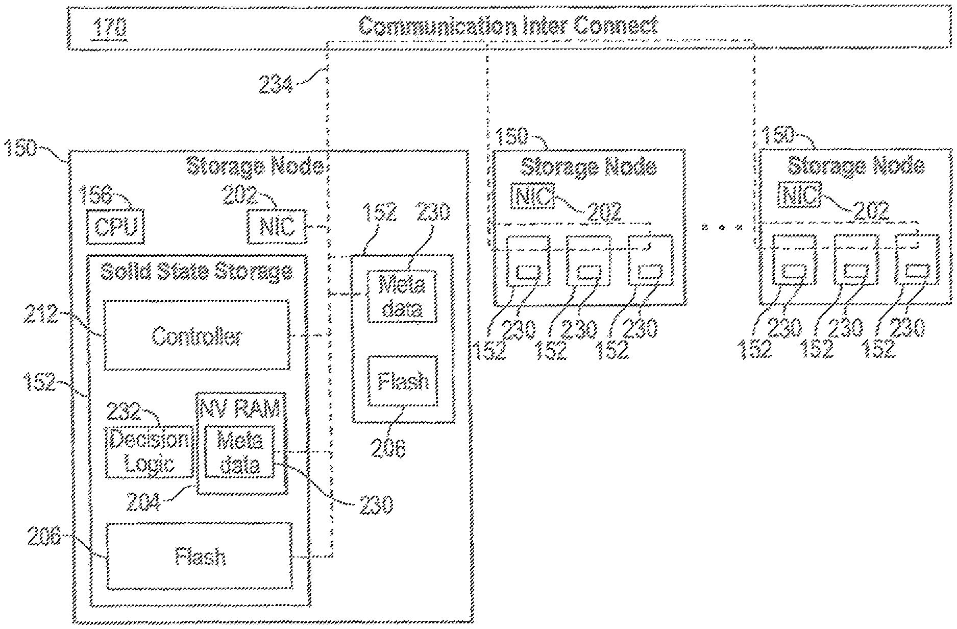
Flash storage nodes 150 are coupled via the communication interconnect 170. More specifically, the network interface controller 202 of each storage node 150 in the storage cluster is coupled to the communication interconnect 170, providing a communication path 234 among storage nodes 150 and non-volatile solid-state storage 152. Storage nodes 150 have one or more non-volatile solid-state storage units 152. Non-volatile solid-state storage units 152 internal to a storage node can communicate with each other, for example via a bus, a serial communication path, a network path or other communication path 234 as readily devised in accordance with the embodiments disclosed herein. Communication interconnect 170 can be included in or implemented with the switch fabric of FIG. 1 in some embodiments. Storage nodes 150 of FIG. 4 form a storage cluster that is enclosed within a single chassis that has an internal power distribution bus within the chassis as described with reference to FIG. 1.
Referring to FIGS. 3 and 4, in case of a power failure, whether local to non-volatile solid-state storage 152 or a storage node 150, data can be copied from the NVRAM 204 to the flash memory 206. For example, the DMA unit 214 of FIG. 3 can copy contents of the NVRAM 204, including the metadata, to the flash memory 206, using power supplied by the energy reserve 218. Energy reserve 218 is sized with sufficient capacity to support copy operation. That is, the energy reserve 218 should be sized so as to provide sufficient current at a sufficient voltage level for a time duration long enough to complete the copying so that messages that are in metadata 230 are persisted in the flash memory 206.
A further mechanism for persisting messages in a storage system involves the communication path 234 described above in FIG. 4. Redundant copies of the metadata 230 can be distributed via the communication path 234, in various ways. For example, a message coming from the filesystem could be distributed via the communication interconnect 170 as a broadcast over the communication path 234 to all of the non-volatile solid-state storages 152. A non-volatile solid-state storage 152 could send a copy of metadata 230 over the communication path 234 to other non-volatile solid-state storage 152 in a storage node 150. CPU 156 on a storage node 150, receiving a message from the communication interconnect 170 via the network interface controller 202 could send a copy of the message to each solid-state storage 152. The CPU 156 may rebroadcast the message to other flash storage nodes 150, and the flash storage nodes 150 could then distribute the message to the solid-state storages 152 in each of these flash storage nodes 150 in some embodiments. In these and other uses of the communication path 234, redundant copies of the metadata 230 can be distributed to the non-volatile solid-state storages 152. Then, if one non-volatile solid-state storage 152, or one storage node 150 experiences a failure, redundant copies of any message are available in metadata 230 of at least one other non-volatile solid-state storage 152. Each non-volatile solid-state storage 152 can apply decision logic 232 when evaluating various situations such as local power failure, an unreachable node, or instructions to consider or commence a data recovery or a data rebuild. The decision logic 232 includes witnessing logic, voting logic, consensus logic and/or other types of decision logic in various embodiments. Decision logic 232 could be implemented in hardware, software executing on the controller 212, firmware, or combinations thereof, and could be implemented as part of the controller 212 or coupled to the controller 212. The decision logic 232 is employed in consensus decisions among multiple solid-state storage units 152, in some embodiments. In further embodiments, the decision logic 232 could cooperate with the other non-volatile solid-state storage units 152 in order to gather copies of the redundant metadata 230, and make local decisions. The mechanisms for persisting messages in a storage system are useful in the event of a failure, and can be used in data recovery and reconstruction as described above.
Examples of messages include a request to write data, a request to read data, a request to lock or unlock a file, a change in permission of a file, an update to a file allocation table or other file or directory structure, a request to write a file that has executable instructions or to write a file name that is reserved and interpreted as an executable direction, updates to one or more authorities, updates to a fingerprint table, list or other data used in deduplication, updates to hash tables, updates to logs, and so on. When a message is received in non-volatile solid-state storage 152 of a storage node 150, indicating some action has taken place, the message or a derivation of the message is stored as metadata 230 in the NVRAM 204 of that solid-state storage 152. By applying the redundant copies of the metadata 230, actions are captured that are in progress, so that if a failure happens, these actions can be replayed and replacement actions can then be performed, for example upon restart. Actions span storage nodes and use cluster messaging, so the act of sending a message can be made persistent data via one or more of the mechanisms for persisting messages. These mechanisms address some of the known failure scenarios in order to ensure availability of data. In some embodiments, the messages don't require permanence beyond completion of the actions. In other embodiments the messages are further retained to facilitate rollback or other recovery operations.
For example, if a command is sent out to carry out a write operation, this message is recorded and redundant. If there is a failure, it can be determined whether or not that action has been carried out, and whether or not the action should be driven to completion. Such determination can be carried out using the decision logic 232 in each non-volatile solid-state storage 152. There is dedicated storage in NVRAM 204 for messages and other metadata 230, so that messages are recorded in the non-volatile solid-state storage 152 and replicated in some embodiments. The messages and other metadata 230 are written into flash memory 206 if one non-volatile solid-state storage 152 experiences a power failure or if the entire system experiences a power failure or otherwise shuts down. The redundancy level of the messages matches the redundancy level of the metadata in some embodiments. When there are sufficient numbers of copies of messages, the message becomes irrevocable. If one node goes down, other nodes can vote, achieve consensus, or witness the various copies of the message and determine what action, if any, to carry to completion. If the entire system goes down, e.g., through a global power failure, then a sufficient number of these messages get written from NVRAM 204 to flash memory 206. Upon restoration of power, the nodes can again open copies of the message and determine what action, if any, to carry to completion to prevent any corruption.
With continued reference to FIGS. 3 and 4, storage node 150 of a storage cluster 160 includes two levels of controllers. There is a host CPU 156 in the storage node 150, and there is a controller 212 in the non-volatile solid-state storage 152. The controller 212 can be considered a flash memory controller, which serves as a bridge between the host CPU 156 and the flash memory 206. Each of these controllers, namely the host CPU 156 and the flash controller 212, can be implemented as one or more processors or controllers of various types from various manufacturers. The host CPU 156 can access both the flash memory 206 and the NVRAM 204 as distinct resources, with each being independently (i.e., individually) addressable by the host CPU 156.
By separating the NVRAM 204 and the flash memory 206 into distinct resources, not all data placed in the NVRAM 204 must be written to the flash memory 206. The NVRAM 204 can also be employed for various functions and purposes. For example, updates to the NVRAM 204 can be made obsolete by newer updates to the NVRAM 204. A later transfer of user data from the NVRAM 204 to the flash memory 206 can transfer the updated user data, without transferring the obsolete user data to the flash memory 206. This reduces the number of erasure cycles of the flash memory 206, reduces wear on the flash memory 206, and moves data more efficiently. The CPU 156 can write to the NVRAM 204 at a smaller granularity than the granularity of the transfers from the NVRAM 204 to the flash memory 206. For example, the CPU 156 could perform 4 kB writes to the NVRAM 204, and the DMA unit 214 could perform a page write of 16 kB from the NVRAM 204 to the flash memory 206 under direction of the controller 212. The ability to collect multiple writes of user data to the NVRAM 204 prior to writing the user data from the NVRAM 204 to the flash memory 206 increases writing efficiency. In some embodiments, a client write of user data is acknowledged at the point at which the user data is written to the NVRAM 204. Since the energy reserve 218, described above with reference to FIG. 3, provides sufficient power for a transfer of contents of the NVRAM 204 to the flash memory 206, the acknowledgment of the client write does not need to wait until the user data is written to the flash memory 206.
As further examples of differences between present embodiments and previous solid-state drives, the metadata 230 in the NVRAM 204 is not written into the flash memory 206, except in cases of power loss. Here, a portion of the NVRAM 204 acts as a workspace for the CPU 156 of the storage node 150 to apply the metadata 230. The CPU 156 of the storage node 150 can write to the NVRAM 204 and read the NVRAM 204, in order to access the metadata 230. The CPU 156 is responsible for migrating data from the NVRAM 204 down to the flash memory 206 in one embodiment. Transfer from the NVRAM 204 to the flash memory 206 is not automatic and predetermined, in such embodiments. Transfer waits until there is sufficient user data in the NVRAM 204 for a page write to the flash memory 206, as determined by the CPU 156 and directed to the DMA unit 214. The DMA unit 214 can be further involved in the path of the user data. In some embodiments, the DMA unit 214 (also known as a DMA engine) is designed to detect and understand various data formats. The DMA unit 214 can perform a cyclic redundancy check (CRC) calculation to check the integrity of the user data. In some embodiments, the DMA unit 214 inserts the CRC calculation into the data and verifies that the data is consistent with a previously inserted CRC calculation.
Work may be offloaded to the controller 212 of the non-volatile solid-state storage 152. Processing that is offloaded to flash controller 212 can be co-designed with processing performed by the CPU 156 of the storage node 150. Various mapping tables that translate from one address space to another, e.g., index trees or address translation tables, can be managed within the non-volatile solid-state storage 152, in some embodiments. The controller 212 of the non-volatile solid-state storage 152 can perform various tasks such as looking through these mapping tables, finding metadata associated with the mapping tables, and determining physical addresses, e.g., for user data sought by the CPU 156 of the storage node 150. In order to find an authority associated with a segment number, a standard solid-state drive might bring back an entire 16 kB flash page, and the CPU 156 would search in this page. In some embodiments, the controller 212 of the non-volatile solid-state storage 152 can perform this search much more efficiently, and pass the results to the CPU 156 of the storage node 150, without sending back the entire flash page to the CPU 156.
FIG. 5 is an address and data diagram showing address translation as applied to user data being stored in an embodiment of a non-volatile solid-state storage 152. In some embodiments, one or more of the address translations applies an address space having nonrepeating addresses. User data, arriving for storage in a storage cluster, is associated with a file path according to a file system. The user data is separated into data segments, each of which is assigned a segment address. Each data segment is separated into data shards, each of which is stored in flash memory 206 (See FIG. 3). Various address translation tables 502 (e.g., mapping tables) are applied by either the CPU of the storage node or the controller of the non-volatile solid-state storage to translate, track and assign addresses to the user data and portions thereof.
These address translation tables 502 reside as metadata in the memory 154 (See FIG. 1) of the storage node, the NVRAM 204 (See FIG. 3) of the non-volatile solid-state storage, and/or the flash memory of the non-volatile solid-state storage, in various embodiments. Generally, address translation tables 502 that occur later in the chain of translations have a greater number of entries (e.g., address translation tables 502D and 502E) and should be located in the flash memory 206, as there may not be sufficient memory space for these in the NVRAM or the memory 154. Further, messages regarding updates to the tables 502, or derivations of these messages, could be stored as metadata in the above-described memories. Metadata in one or more of these locations can be subjected to replication (i.e., redundancy) and decisions for various degrees of fault tolerance and system recovery, as described above.
For a particular portion of user data, the file path is translated or mapped to an inode ID with use of an address translation table 502A. This may be in accordance with a filesystem, and could be performed by the CPU of the storage node in some embodiments. The inode ID is translated or mapped to a medium address with use of an address translation table 502B, which could be performed by CPU. In some embodiments, the medium address, which is in a medium address space, is included as one of the sequential nonrepeating addresses. The medium address is translated or mapped to the segment address, with use of an address translation table 502C through the CPU in some embodiments. The segment address, which is in a segment address space, may be included as one of the sequential nonrepeating addresses. The segment address, as assigned to the data segment, is translated to a virtual allocation unit, as assigned to the data shard, with use of an address translation table 502D. Controller 212 of the non-volatile solid-state storage may perform this translation by accessing address translation table 502D in the flash memory 206. The virtual allocation unit is translated to a physical flash memory location with the use of an address translation table 502E. The physical flash memory location may be assigned to the data shard.
The address space with the sequential nonrepeating addresses may be applied to the medium address space, the segment address space and/or the virtual allocation unit address space in various embodiments. In each case, a range of addresses from the address space is assigned to each of the non-volatile solid-state storages in a storage cluster, or to each of the storage nodes in a storage cluster. The ranges may be non-overlapping, such that each non-volatile solid-state storage unit is assigned a range that differs from the ranges of the other non-volatile solid-state storage units. In this mechanism, no address from this address space repeats anywhere in the storage cluster. That is, each address from this address space is unique, and no two portions of user data are assigned the same address from this address space, during the expected lifespan of the system. Each time one of the addresses from this address space is assigned to a portion of user data in a non-volatile solid-state storage unit, whether the address is a medium address, a segment address, or a virtual allocation unit, the address (upon assignment) should be logically greater than all such addresses previously assigned in that non-volatile solid-state storage unit. Thus, the addresses may be referred to as sequential nonrepeating in this address space. The address space with these properties could include the medium address space, the segment address space and/or the virtual allocation unit address space. A non-volatile solid-state storage unit can allocate the assigned range of addresses in the non-volatile solid-state storage without synchronization with other non-volatile solid-state storage units in a storage cluster.
Each range of the address space has upper and lower bounds in some embodiments. Overall, the address space has an upper bound that exceeds the likely maximum address that would be assigned during the expected lifespan of a system. In one embodiment, the sequential nonrepeating addresses in the address space are binary numbers with at least 128 bits. The amount of bits may vary in embodiments, however with 128 bits, two raised to the 128.sup.th power is greater than the expected maximum address occurring for the lifetime of the system. The upper bound of the address space is greater than or equal to this number, or could include or be this number, in some embodiments. Larger numbers could be applied as technology further advances to higher operating speeds and lower time delays for reading and/or writing. The lower bound of the address space could be zero or one, or some other suitable low number.
Applying the nonrepeating addresses to one or more of the medium addresses, the segment addresses, or the virtual allocation units, enhance data recovery and flash writes. In some embodiments, the storage cluster, the storage node or the non-volatile, solid-state storage unit performs a snapshot of the present contents of the cluster, the storage node, or the non-volatile solid-state storage unit. At a later time, a particular version of user data can be recovered by referring to the snapshot. Since the relevant addresses do not have duplicates, there is an unambiguous record of the version of the user data at the time of the snapshot, and data is readily recovered if still existing in the relevant memory. Formats for snapshots are readily devised, and may include a file with a record of the contents of the cluster, the storage node, or the non-volatile solid-state storage unit, applying one or more address schemes. Depending on which address scheme or schemes is present in the snapshot, the address translation tables 502A, 502B, 502C, 502D, 502E can be applied to determine physical flash memory locations and presence or absence in the flash memory 206 of the desired data for recovery.
For flash writes, in some embodiments blocks of flash pages 224 are erased, and then individual flash pages 224 (see FIG. 3) are written in sequential order within a single erased block. This operation is supported by the above-described addressing mechanism, which assigns sequentially increasing or decreasing addresses to data segments and/or data shards as they arrive for storage in some embodiments. In some embodiments, information relating to the medium address, the segment address, and/or the virtual allocation unit is written to a header of the flash page 224, thus identifying data stored in the flash page 224 (e.g., as data shards). The flash page 224, in such embodiments, becomes self-describing and self-checking, via the information in the header.
FIG. 6 is a block diagram showing a DMA unit 214 transferring data that has a self-describing data format, in an embodiment of the non-volatile solid-state storage unit of FIGS. 1-5. The DMA unit 214 communicates with the NVRAM 204 and the flash memory 206, as described above with reference to FIG. 3. User data is broken up, e.g. into segments and shards, and mapped to physical locations in flash memory 206, as described above with reference to FIGS. 4 and 5. In the embodiment shown in FIG. 6, a self-describing data portion 602 is written into NVRAM 204, e.g. by the CPU of the storage node or the controller of the non-volatile solid-state storage. The NVRAM 204 in each non-volatile solid-state storage unit can have many self-describing data portions 602. In various scenarios, the DMA unit 214 is instructed to transfer portions or all of the contents of the NVRAM 204 to the flash memory 206, which could happen during data storage, or during loss of power as described above.
Still referring to FIG. 6, the self-describing data portion 602, in the NVRAM 204, has a destination section 604, a status section 606, and data 608. The data 608 could be in the form of a data shard as described above. The destination section 604 includes destination information, from which a destination can be extracted by the DMA unit 214. This destination information could be an address, a destination pointer, or an offset in flash memory 206, e.g., an offset relative to a flash page 224. With the destination section 604, the data 608 becomes self-describing as to where the data is destined to be stored. The destination pointer or some offset is encoded into the data itself, i.e., into the self-describing data portion 602. DMA unit 214 determines from the encoded pointer or offset where to place the data when writing. The status section 606 includes status information about the data 608, such as whether or not the data 608 has been written to the flash memory 206, or whether or not the data 608 will be used. In a situation where the data 608 will not be used, the data 608 does not need to be transferred to the flash memory 206. This may occur when the data 608 is obsolete, for example by a user action or system action of deleting a file. The data also may not be used when a file is revised, and the revised portions of the file are stored elsewhere, superseding this particular data 608. The data 608, the status section 606, the destination section 604, and/or further information can be in various orders and sequences in embodiments of the self-describing data portion 602.
The DMA unit 214 extracts a destination from the destination section 604 of the self-describing data portion 602. The DMA unit 214 also extracts status information from the status section 606 of the self-describing data portion 602, by reading specified portions or fields of the self-describing data portion 602 in some embodiments. For example, the DMA unit 214 could read the entire self-describing data portion 602 from the NVRAM 204, and mask various sections, or transfer various sections to local memory or registers, etc. As a further example, the DMA unit 214 could read only the destination section 604, the status section 606, or the data 608 from the NVRAM 204 in some embodiments. The DMA unit 214 acts according to information that is read. If the DMA unit 214 determines that the data 608 is valid and has not yet been transferred to the flash memory 206, the DMA unit 214 performs the transfer. The DMA unit 214 reads the data 608 from the self-describing data portion 602 in the NVRAM 204, and writes the data 608 to the destination in a flash page 224 in the flash memory 206. If the DMA unit 214 determines that the data 608 does not need to be transferred to the flash memory 206, according to the status information extracted from the status section 606, the DMA unit 214 may transfer other data, but not that particular data 608. In other words, the DMA unit 214 does not need to rewrite the data 608 into the flash memory 206 if the data 608 has already been transferred to the flash memory 206. In addition, the DMA unit 214 does not need to write the data 608 into the flash memory 206 if the status section 606 indicates the data 608 will not be used.
In some embodiments of FIG. 6, the DMA unit 214 writes an update to the status section 606 of the self-describing data portion 602 in the NVRAM 204, after writing the data 608 into the flash memory 206. This update confirms and indicates the data 608 has been written into the flash memory 206. Such an indication serves to notify the DMA unit 214 that, in case of power loss, the DMA unit 214 does not need to write the data 608 into the flash memory 206, as this has already been done. This indication also serves to notify the CPU of the storage node and the controller of the non-volatile solid-state storage unit that the location in NVRAM 204 of the self-describing data portion 602 is now available for a new self-describing data portion 602. Garbage collection or other system processes can make use of the status section 606, in order to recover or reuse memory space in the NVRAM 204. In some embodiments, the DMA unit writes an identifier to the header 610 of the flash page 224. The identifier identifies the data 608 written to the flash page 224. The identifier may include an inode ID, a medium address, a segment ID and/or an offset into the flash page 224, any or all of which point to the data 608 and support access to the data 608. Various embodiments of the nonvolatile solid-state storage 152 and other storages use various combinations of the above-described features.
FIG. 7 is a flow diagram of a method for applying a self-describing data format to a direct memory access transfer, which can be applied to or by embodiments of storage clusters, storage nodes and/or non-volatile solid-state storage units as described herein. The method initiates with one or more self-describing data portions written to NVRAM in action 702. This can be performed by a processor, such as a CPU of the data node or a controller of the non-volatile solid-state storage. For example, these data portions could be large amounts of data, small amount of data, data segments, or data shards. The remaining actions 704-718 of the method can be performed by a DMA unit of the non-volatile solid-state storage. In further embodiments, these actions can be performed by other processors and/or other DMA units acting on other types of memory as the embodiments provide examples not meant to be limiting. In an action 704, a destination is obtained from a self-describing data portion. For example, the DMA unit could extract the destination from a destination section of a self-describing data portion in NVRAM. In an action 706, status information is obtained from the self-describing data portion. The status information may be extracted from the status section of the self-describing data portion in NVRAM, before, after, or in parallel with the extraction of the destination.
The method of FIG. 7 advances to decision action 708, where it is determined if data is to be transferred to flash. The DMA unit may determine from the status information whether or not the data is valid and/or whether or not the data has already been transferred to flash. The determination could be indicated by one or more status bits in various formats as readily devised in accordance with the teachings herein. If the answer is no, the data should not be transferred to flash, flow branches to the decision action 716. This could be the case if the data is obsolete, or if the data has already been transferred to flash. If the answer is yes, the data should be transferred to flash, flow continues to the action 710. Data is written to the destination in flash, in the action 710. This can be accomplished by the DMA unit reading the data from the self-describing data portion in NVRAM, determining the destination in the action 704, and writing the data to that destination in some embodiments. An identifier is written to the header of the flash page, in an action 712. The status is updated in the self-describing data portion in NVRAM, in an action 714. For example, the DMA unit could write to the self-describing data portion in NVRAM, to indicate in the status section that the data has been written successfully to the flash.
In a decision action 716, it is determined if there a power loss. If the answer is no, flow branches back to the action 704, to obtain a destination for another self-describing data portion. Alternatively, flow could branch back to the action 702, in order for a new self-describing data portion to be written to the NVRAM. If the answer is yes, there is a power loss, flow continues to the action 718. In the action 718, portions of the NVRAM are transferred to flash, unless already transferred. This action can be accomplished with a process similar to the actions 704-714, or variations thereof. The process goes to an endpoint after the transfer, at which time the energy reserve apparatus applied during power loss may be exhausted. In further embodiments, with a longer power reserve, further processes may be initiated and completed.
It should be appreciated that the methods described herein may be performed with a digital processing system, such as a conventional, general-purpose computer system. Special purpose computers, which are designed or programmed to perform only one function may be used in the alternative. FIG. 8 is an illustration showing an exemplary computing device which may implement the embodiments described herein. The computing device of FIG. 8 may be used to perform embodiments of the functionality for a storage node or a non-volatile solid-state storage in accordance with some embodiments. The computing device includes a central processing unit (CPU) 801, which is coupled through a bus 805 to a memory 803, and mass storage device 807. Mass storage device 807 represents a persistent data storage device such as a disc drive, which may be local or remote in some embodiments. The mass storage device 807 could implement a backup storage, in some embodiments. Memory 803 may include read only memory, random access memory, etc. Applications resident on the computing device may be stored on or accessed via a computer readable medium such as memory 803 or mass storage device 807 in some embodiments. Applications may also be in the form of modulated electronic signals modulated accessed via a network modem or other network interface of the computing device. It should be appreciated that CPU 801 may be embodied in a general-purpose processor, a special purpose processor, or a specially programmed logic device in some embodiments.
Display 811 is in communication with CPU 801, memory 803, and mass storage device 807, through bus 805. Display 811 is configured to display any visualization tools or reports associated with the system described herein. Input/output device 809 is coupled to bus 805 in order to communicate information in command selections to CPU 801. It should be appreciated that data to and from external devices may be communicated through the input/output device 809. CPU 801 can be defined to execute the functionality described herein to enable the functionality described with reference to FIGS. 1-7. The code embodying this functionality may be stored within memory 803 or mass storage device 807 for execution by a processor such as CPU 801 in some embodiments. The operating system on the computing device may be MS-WINDOWS.TM., UNIX.TM., LINUX.TM., iOS.TM., CentOS.TM., Android.TM., Redhat Linux.TM., z/OS.TM., or other known operating systems. It should be appreciated that the embodiments described herein may be integrated with virtualized computing system also.
Detailed illustrative embodiments are disclosed herein. However, specific functional details disclosed herein are merely representative for purposes of describing embodiments. Embodiments may, however, be embodied in many alternate forms and should not be construed as limited to only the embodiments set forth herein.
It should be understood that although the terms first, second, etc. may be used herein to describe various steps or calculations, these steps or calculations should not be limited by these terms. These terms are only used to distinguish one step or calculation from another. For example, a first calculation could be termed a second calculation, and, similarly, a second step could be termed a first step, without departing from the scope of this disclosure. As used herein, the term "and/or" and the "/" symbol includes any and all combinations of one or more of the associated listed items.
As used herein, the singular forms "a", "an" and "the" are intended to include the plural forms as well, unless the context clearly indicates otherwise. It will be further understood that the terms "comprises", "comprising", "includes", and/or "including", when used herein, specify the presence of stated features, integers, steps, operations, elements, and/or components, but do not preclude the presence or addition of one or more other features, integers, steps, operations, elements, components, and/or groups thereof. Therefore, the terminology used herein is for the purpose of describing particular embodiments only and is not intended to be limiting.
It should also be noted that in some alternative implementations, the functions/acts noted may occur out of the order noted in the figures. For example, two figures shown in succession may in fact be executed substantially concurrently or may sometimes be executed in the reverse order, depending upon the functionality/acts involved.
With the above embodiments in mind, it should be understood that the embodiments might employ various computer-implemented operations involving data stored in computer systems. These operations are those requiring physical manipulation of physical quantities. Usually, though not necessarily, these quantities take the form of electrical or magnetic signals capable of being stored, transferred, combined, compared, and otherwise manipulated. Further, the manipulations performed are often referred to in terms, such as producing, identifying, determining, or comparing. Any of the operations described herein that form part of the embodiments are useful machine operations. The embodiments also relate to a device or an apparatus for performing these operations. The apparatus can be specially constructed for the required purpose, or the apparatus can be a general-purpose computer selectively activated or configured by a computer program stored in the computer. In particular, various general-purpose machines can be used with computer programs written in accordance with the teachings herein, or it may be more convenient to construct a more specialized apparatus to perform the required operations.
A module, an application, a layer, an agent or other method-operable entity could be implemented as hardware, firmware, or a processor executing software, or combinations thereof. It should be appreciated that, where a software-based embodiment is disclosed herein, the software can be embodied in a physical machine such as a controller. For example, a controller could include a first module and a second module. A controller could be configured to perform various actions, e.g., of a method, an application, a layer or an agent.
The embodiments can also be embodied as computer readable code on a non-transitory computer readable medium. The computer readable medium is any data storage device that can store data, which can be thereafter read by a computer system. Examples of the computer readable medium include hard drives, network attached storage (NAS), read-only memory, random-access memory, CD-ROMs, CD-Rs, CD-RWs, magnetic tapes, and other optical and non-optical data storage devices. The computer readable medium can also be distributed over a network coupled computer system so that the computer readable code is stored and executed in a distributed fashion. Embodiments described herein may be practiced with various computer system configurations including hand-held devices, tablets, microprocessor systems, microprocessor-based or programmable consumer electronics, minicomputers, mainframe computers and the like. The embodiments can also be practiced in distributed computing environments where tasks are performed by remote processing devices that are linked through a wire-based or wireless network.
Although the method operations were described in a specific order, it should be understood that other operations may be performed in between described operations, described operations may be adjusted so that they occur at slightly different times or the described operations may be distributed in a system which allows the occurrence of the processing operations at various intervals associated with the processing.
In various embodiments, one or more portions of the methods and mechanisms described herein may form part of a cloud-computing environment. In such embodiments, resources may be provided over the Internet as services according to one or more various models. Such models may include Infrastructure as a Service (IaaS), Platform as a Service (PaaS), and Software as a Service (SaaS). In IaaS, computer infrastructure is delivered as a service. In such a case, the computing equipment is generally owned and operated by the service provider. In the PaaS model, software tools and underlying equipment used by developers to develop software solutions may be provided as a service and hosted by the service provider. SaaS typically includes a service provider licensing software as a service on demand. The service provider may host the software, or may deploy the software to a customer for a given period of time. Numerous combinations of the above models are possible and are contemplated.
Various units, circuits, or other components may be described or claimed as "configured to" perform a task or tasks. In such contexts, the phrase "configured to" is used to connote structure by indicating that the units/circuits/components include structure (e.g., circuitry) that performs the task or tasks during operation. As such, the unit/circuit/component can be said to be configured to perform the task even when the specified unit/circuit/component is not currently operational (e.g., is not on). The units/circuits/components used with the "configured to" language include hardware--for example, circuits, memory storing program instructions executable to implement the operation, etc. Reciting that a unit/circuit/component is "configured to" perform one or more tasks is expressly intended not to invoke 35 U.S.C. 112, sixth paragraph, for that unit/circuit/component. Additionally, "configured to" can include generic structure (e.g., generic circuitry) that is manipulated by software and/or firmware (e.g., an FPGA or a general-purpose processor executing software) to operate in manner that is capable of performing the task(s) at issue. "Configured to" may also include adapting a manufacturing process (e.g., a semiconductor fabrication facility) to fabricate devices (e.g., integrated circuits) that are adapted to implement or perform one or more tasks.
The foregoing description, for the purpose of explanation, has been described with reference to specific embodiments. However, the illustrative discussions above are not intended to be exhaustive or to limit the invention to the precise forms disclosed. Many modifications and variations are possible in view of the above teachings. The embodiments were chosen and described in order to best explain the principles of the embodiments and its practical applications, to thereby enable others skilled in the art to best utilize the embodiments and various modifications as may be suited to the particular use contemplated. Accordingly, the present embodiments are to be considered as illustrative and not restrictive, and the invention is not to be limited to the details given herein, but may be modified within the scope and equivalents of the appended claims.
* * * * *
References
D00000
D00001
D00002
D00003
D00004
D00005
D00006
D00007
D00008
XML
uspto.report is an independent third-party trademark research tool that is not affiliated, endorsed, or sponsored by the United States Patent and Trademark Office (USPTO) or any other governmental organization. The information provided by uspto.report is based on publicly available data at the time of writing and is intended for informational purposes only.
While we strive to provide accurate and up-to-date information, we do not guarantee the accuracy, completeness, reliability, or suitability of the information displayed on this site. The use of this site is at your own risk. Any reliance you place on such information is therefore strictly at your own risk.
All official trademark data, including owner information, should be verified by visiting the official USPTO website at www.uspto.gov. This site is not intended to replace professional legal advice and should not be used as a substitute for consulting with a legal professional who is knowledgeable about trademark law.