Enhancement mode high electron mobility transistor (HEMT)
Shrivastava , et al. November 17, 2
U.S. patent number 10,840,348 [Application Number 16/114,650] was granted by the patent office on 2020-11-17 for enhancement mode high electron mobility transistor (hemt). This patent grant is currently assigned to Indian Institute of Science. The grantee listed for this patent is INDIAN INSTITUTE OF SCIENCE. Invention is credited to Navakanta Bhat, Sayak Dutta Gupta, Srinivasan Raghavan, Mayank Shrivastava, Ankit Soni.


View All Diagrams
| United States Patent | 10,840,348 |
| Shrivastava , et al. | November 17, 2020 |
Enhancement mode high electron mobility transistor (HEMT)
Abstract
The present disclosure provides an improved enhancement mode field effect transistor (FET) having an oxide (Al.sub.xTi.sub.1-xO) emulating p-type gate. The present disclosure provides a novel enhancement mode High Electron Mobility Transistor (HEMT) structure with Al.sub.xTi.sub.1-xO Gate Oxide Engineering as Replacement of p-GaN Gate. In an aspect, the present disclosure provides a hybrid gate stack that combines p-GaN technology with the proposed oxide for e-mode operation. The HEMT structure with Al.sub.xTi.sub.1-xO Gate oxide provides a threshold voltage tuning from negative to positive by changing p-doping composition. Using a developed p-type oxide, e-mode device shows ON current .about.400 mA/mm, sub-threshold slope of 73 mV/dec, R.sub.on=8.9 .OMEGA.mm, interface trap density <10.sup.10 mm.sup.-2eV.sup.-1 and gate leakage below 200 nA/mm at the OFF-state breakdown.
| Inventors: | Shrivastava; Mayank (Bangalore, IN), Dutta Gupta; Sayak (Bangalore, IN), Soni; Ankit (Bangalore, IN), Raghavan; Srinivasan (Bangalore, IN), Bhat; Navakanta (Bangalore, IN) | ||||||||||
|---|---|---|---|---|---|---|---|---|---|---|---|
| Applicant: |
|
||||||||||
| Assignee: | Indian Institute of Science
(Karnataka, IN) |
||||||||||
| Family ID: | 1000005187757 | ||||||||||
| Appl. No.: | 16/114,650 | ||||||||||
| Filed: | August 28, 2018 |
Prior Publication Data
| Document Identifier | Publication Date | |
|---|---|---|
| US 20190067440 A1 | Feb 28, 2019 | |
Foreign Application Priority Data
| Aug 29, 2017 [IN] | 201741030570 | |||
| Current U.S. Class: | 1/1 |
| Current CPC Class: | H01L 21/02194 (20130101); H01L 21/02178 (20130101); H01L 29/7786 (20130101); H01L 21/02186 (20130101); H01L 21/0228 (20130101); H01L 29/4983 (20130101); H01L 29/66462 (20130101); H01L 29/517 (20130101); H01L 29/1066 (20130101); H01L 29/2003 (20130101); H01L 29/4236 (20130101) |
| Current International Class: | H01L 29/49 (20060101); H01L 29/66 (20060101); H01L 29/51 (20060101); H01L 21/02 (20060101); H01L 29/778 (20060101); H01L 29/423 (20060101); H01L 29/10 (20060101); H01L 29/20 (20060101) |
References Cited [Referenced By]
U.S. Patent Documents
| 7379322 | May 2008 | Min |
| 7588988 | September 2009 | Ahn |
| 8154066 | April 2012 | Ahn |
| 8541276 | September 2013 | Ahn |
| 9443938 | September 2016 | Mishra |
| 9859413 | January 2018 | Okita |
| 2003/0045082 | March 2003 | Eldridge |
| 2006/0043504 | March 2006 | Ahn |
| 2007/0090441 | April 2007 | Ahn |
| 2009/0146185 | June 2009 | Suh |
| 2010/0155720 | June 2010 | Kaneko |
| 2012/0112202 | May 2012 | Hwang |
| 2012/0196448 | August 2012 | Ahn |
| 2016/0308023 | October 2016 | Hsu |
Attorney, Agent or Firm: Greer Burns & Crain Ltd.
Claims
We claim:
1. A transistor comprising: a source; a drain; and a hybrid gate stack that comprises Al.sub.xTi.sub.1-xO that is an oxide that demonstrates p-type behaviour, wherein said Al.sub.xTi.sub.1-xO demonstrates p-type behaviour by positioning a conduction band above a fermi level in a channel region, that is used as a control parameter to deplete two dimensional electron gas (2DEG) in the channel; and wherein said hybrid gate stack is supported by an AlGaN/GaN stack, and wherein the hybrid gate stack is brought closer to a channel by partial removal of an AlGaN barrier under said hybrid gate stack, followed by deposition of said Al.sub.xTi.sub.1-xO.
2. The transistor as claimed in 1, wherein said Al.sub.xTi.sub.1-xO is formed by Al doping of TiO.sub.2 so as to impact said p-type behaviour to said oxide.
3. The transistor as claimed in claim 1, wherein said transistor is a High Electron Mobility Transistor (HEMT).
4. The transistor as claimed in claim 1, wherein Al content in said oxide is a controlling parameter for a threshold voltage.
5. The transistor as claimed in claim 1, wherein the hybrid gate stack further comprises a p-type GaN cap.
6. The transistor as claimed in claim 1, wherein said transistor is operated in an enhancement mode.
7. A transistor comprising: a source; a drain; and a hybrid gate stack that comprises one or more p-type metal oxides, wherein the one or more p-type metal oxides demonstrate p-type behaviour by positioning a conduction band above a fermi level in a channel region; and wherein the hybrid gate stack is supported by an AlGaN/GaN stack, and wherein the hybrid gate stack is brought closer to a channel by partial removal of an AlGaN barrier under said hybrid gate stack, followed by deposition of said p-type metal oxide.
8. The transistor as claimed in claim 7, wherein the hybrid gate stack further comprises a p-type GaN cap.
9. The transistor as claimed in claim 7, wherein the hybrid gate stack further comprises an insulator or dielectric material.
10. A method of making an Al.sub.xTi.sub.1-xO based dielectric that demonstrates p-type behaviour, said method comprising the steps of using atomic layer deposition (ALD) to enable deposition of Al.sub.2O.sub.3 and TiO.sub.2 across a plurality of cycles to introduce Al atoms in TiO.sub.2, wherein said Al.sub.xTi.sub.1-xO demonstrates p-type behaviour by positioning a conduction band above a fermi level in a channel region, that is use as a control parameter to deplete two dimensional electron gas (2DEG) in the channel; and wherein the Al.sub.xTi.sub.1-xO based dielectric is associated with a high electron mobility transistor.
11. The method of claim 10, wherein the method further comprises the step of depositing Al.sub.2O.sub.3 in an ALD chamber using cycles involving introduction of trimethylaluminium (TMA) and H.sub.2O precursors.
12. The method of claim 10, wherein the method further comprises the step of depositing TiO.sub.2 in said ALD chamber using cycles involving introduction of Titanium tetraisopropoxide (TTIP) and H.sub.2O precursors.
Description
TECHNICAL FIELD
The present disclosure relates generally to the field of field effect transistors (FET). In particular, the present disclosure relates to gate engineering in High Electron Mobility Transistors (HEMT) for improved enhancement mode performance.
BACKGROUND
Background description includes information that may be useful in understanding the present invention. It is not an admission that any of the information provided herein is prior art or relevant to the presently claimed invention, or that any publication specifically or implicitly referenced is prior art.
A high-electron-mobility transistor (HEMT), also known as heterostructure FET (HFET) or modulation-doped FET (MODFET), is a field-effect transistor (FET) that incorporates a junction between two materials that have different band gaps (i.e. a heterojunction) as the channel instead of a doped region (as is generally the case for MOSFET). A commonly used material combination is Gallium arsenide (GaAs) with Aluminium gallium arsenide (AlGaAs), though there is wide variation in such combinations depending on the application of the device. Devices incorporating more indium generally show better high-frequency performance, while in recent years, gallium nitride HEMTs have attracted attention due to their high-power performance.
Normally OFF Aluminium gallium nitride (AlGaN)/gallium nitride (GaN) HEMTs have emerged as efficient switching devices in the growing power semiconductor market. The major bottleneck is to have an effective method for depleting the channel so that it does not degrade device characteristics. There have been several approaches proposed over time for turning off the HEMT channel, namely recessed gate, F.sup.- ion implanted gate and p-GaN gate structures, but such approaches have repercussions that are imperative to device performance. For example, complete etching of AlGaN barrier leads to Two-Dimensional Electron Gas (2DEG) depletion, but the resultant device suffers from degraded on-state performance such as low channel mobility, high ON-state resistance and poor reliability. Fluorine ion implantation under gate has been another widely-adopted technique but F.sup.--ion stability under high stress or temperature condition is still questionable. Using a thick p-GaN cap to deplete 2DEG can effectively weaken the gate drive and device performance. All these methods/approaches are sufficient for turning-off the device, but still are placed far away when accounted for the variability, consistency and long-term reliability.
Also, Enhancement mode (E-mode), or normally-OFF devices, based on Gallium Nitride (GaN) technology are interesting for a variety of applications such as in integration of control circuitry and for added safety of a normally-OFF device in power switching applications. As already known in the art, enhancement mode operation is commonly achieved using an AlGaN/GaN buffer structure by etching away some of the AlGaN under the gate region until all the charge is depleted, or by exposing the AlGaN under the gate with fluoride-based plasma until negatively charged fixed fluorine ions screen all the charge in the channel. However, these devices suffer from threshold voltage non-uniformity and repeatability due to the processes requiring gate recess etch or plasma treatment. Also, these devices have a low Schottky gate turn-on voltage (of at most 2 V) due to low Schottky barriers. If a threshold voltage of 1V is required, these devices are left with a maximum modulation of 1V. Because high-power switching applications require a threshold voltage of over 1V for gate signal noise immunity, increasing gate turn-on voltage is crucial. Further, utilization of p-GaN barrier below the gate is also known in the prior-art, wherein such utilization depletes channel and increases gate turn-on voltage to 3V, rendering it attractive for high-power applications. However, such field effect devices suffer from high ON-resistance.
The exploration for a novel technique that mitigates above-mentioned limitations and enhances performance in normally-OFF condition is still continued. There is therefore a need to provide a new, improved, efficient, and technically advanced HEMT device that can provide a replacement of p-GaN gate and can help mitigate the above-mentioned limitations, along with enhancing performance in normally-OFF condition. Further, there is also a need to provide an HEMT device that demonstrates threshold voltage tuning from negative to positive by changing p-doping composition, and/or high performance with ON current, and/or low sub-threshold slope, and/or low interface trap density, and/or low gate leakage at the OFF-state breakdown.
In some embodiments, numerical parameters set forth in the written description and attached claims are approximations that can vary depending upon the desired properties sought to be obtained by a particular embodiment. In some embodiments, the numerical parameters should be construed in light of the number of reported significant digits and by applying ordinary rounding techniques. Notwithstanding that the numerical ranges and parameters setting forth the broad scope of some embodiments of the invention are approximations, the numerical values set forth in the specific examples are reported as precisely as practicable. The numerical values presented in some embodiments of the invention may contain certain errors necessarily resulting from the standard deviation found in their respective testing measurements.
As used in the description herein and throughout the claims that follow, the meaning of "a," "an," and "the" includes plural reference unless the context clearly dictates otherwise. Also, as used in the description herein, the meaning of "in" includes "in" and "on" unless the context clearly dictates otherwise.
The recitation of ranges of values herein is merely intended to serve as a shorthand method of referring individually to each separate value falling within the range. Unless otherwise indicated herein, each individual value is incorporated into the specification as if it were individually recited herein. All methods described herein can be performed in any suitable order unless otherwise indicated herein or otherwise clearly contradicted by context. The use of any and all examples, or exemplary language (e.g. "such as") provided with respect to certain embodiments herein is intended merely to better illuminate the invention and does not pose a limitation on the scope of the invention otherwise claimed. No language in the specification should be construed as indicating any non-claimed element essential to the practice of the invention.
Groupings of alternative elements or embodiments of the invention disclosed herein are not to be construed as limitations. Each group member can be referred to and claimed individually or in any combination with other members of the group or other elements found herein. One or more members of a group can be included in, or deleted from, a group for reasons of convenience and/or patentability. When any such inclusion or deletion occurs, the specification is herein deemed to contain the group as modified thus fulfilling the written description of all groups used in the appended claims.
OBJECTS
A general object of the present disclosure is to provide a field effect transistor (FET) operating in enhancement mode (e-mode).
Another object of the present disclosure is to provide an FET with a tunable threshold voltage.
Another object of the present disclosure is to provide an FET with a gate oxide which emulates p-type behaviour.
SUMMARY
The present disclosure relates generally to the field of field effect transistors (FET). In particular, the present disclosure relates to gate engineering in normally OFF High Electron Mobility Transistors (HEMT) for improved enhancement mode performance.
In an aspect, the present disclosure provides a transistor comprising: a source; a drain; and a hybrid gate stack that demonstrates p-type behaviour. In an embodiment, the hybrid gate stack comprises Al.sub.xTi.sub.1-xO. In another embodiment, the transistor is a High Electron Mobility Transistor (HEMT).
In another aspect, the Al.sub.xTi.sub.1-xO is formed by Al doping of TiO.sub.2 so as to impart said p-type behaviour to said oxide.
In another aspect, the Al.sub.xTi.sub.1-xO demonstrates said p-type behaviour by positioning conduction band above Fermi level in the channel region, that is used as a control parameter to deplete 2DEG in channel. In another aspect, Al content in said oxide is used as controlling parameter for threshold voltage.
In another aspect, the hybrid gate stack further comprises a p-type GaN cap.
In another aspect, the hybrid gate stack is supported by an AlGaN/GaN stack, wherein the hybrid gate stack is brought closer to channel by partial removal of AlGaN barrier under said hybrid gate stack, followed by deposition of said Al.sub.xT.sub.1-xO.
In another aspect, the transistor is operated in enhancement mode (e-mode).
In another aspect, the present disclosure provides a transistor comprising: a source; a drain; and a hybrid gate stack that comprises one or more p-type metal oxides.
In another aspect, the hybrid gate stack is supported by an AlGaN/GaN stack, wherein the hybrid gate stack is brought closer to channel by partial removal of AlGaN barrier under said hybrid gate stack, followed by deposition of said p-type metal oxide.
In another aspect, the hybrid gate stack further comprises a p-type GaN cap.
In another aspect, the hybrid gate stack further comprises an oxide material. In another aspect, the present disclosure provides a method for making an Al.sub.xTi.sub.1-xO based oxide that demonstrates p-type behaviour, said method comprising the steps of using atomic layer deposition (ALD) to enable deposition of Al.sub.2O.sub.3 and TiO.sub.2 across a plurality of cycles to introduce Al atoms in TiO.sub.2.
In another aspect, the method further comprises the step of depositing Al.sub.2O.sub.3 in ALD chamber using cycles involving introduction of trimethylaluminium (TMA) and H.sub.2O precursors.
In another aspect, the method further comprises the step of depositing TiO.sub.2 in said ALD chamber using cycles involving introduction of Titanium tetraisopropoxide (TTIP) and H.sub.2O precursors.
Various objects, features, aspects and advantages of the inventive subject matter will become more apparent from the following detailed description of preferred embodiments, along with the accompanying drawing figures in which like numerals represent like components.
BRIEF DESCRIPTION OF THE DRAWINGS
The accompanying drawings are included to provide a further understanding of the present disclosure and are incorporated in and constitute a part of this specification. The drawings illustrate exemplary embodiments of the present disclosure and, together with the description, serve to explain the principles of the present disclosure.
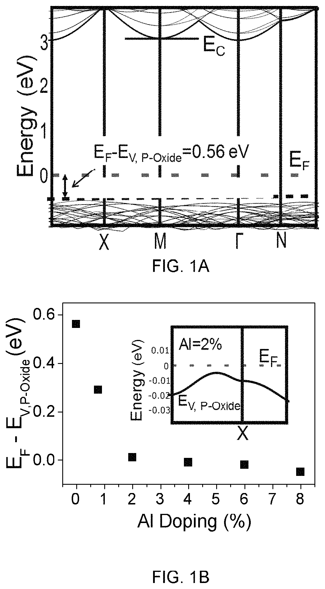
FIG. 1A illustrates band structure of anatase TiO.sub.2 extracted using DFT.
FIG. 1B illustrates shift in Fermi energy level (E.sub.F) towards oxide valence band's energy level (E.sub.V,P-Oxide) with increasing Al % concentration in TiO.sub.2.
FIG. 2A illustrates a cross-sectional view of HEMT with p-type oxide proposed for e-mode operation, in accordance with an exemplary embodiment of the present disclosure.
FIG. 2B illustrates a cross-sectional view of the HEMT with p-type metal oxide gate and partially recessed AlGaN barrier under the gate for e-mode operation, in accordance with an embodiment of the present disclosure.
FIGS. 3A and 3B illustrate energy-band diagram of AlGaN/GaN HEMTs with conventional oxides and with the proposed p-type oxide, respectively.
FIGS. 4A-4C illustrate energy band diagrams, shift of Fermi energy level away from conduction band in the channel and resulting shift in threshold voltage respectively, as a function of p-oxide thickness and energy difference between oxide's Fermi and valence bands levels.
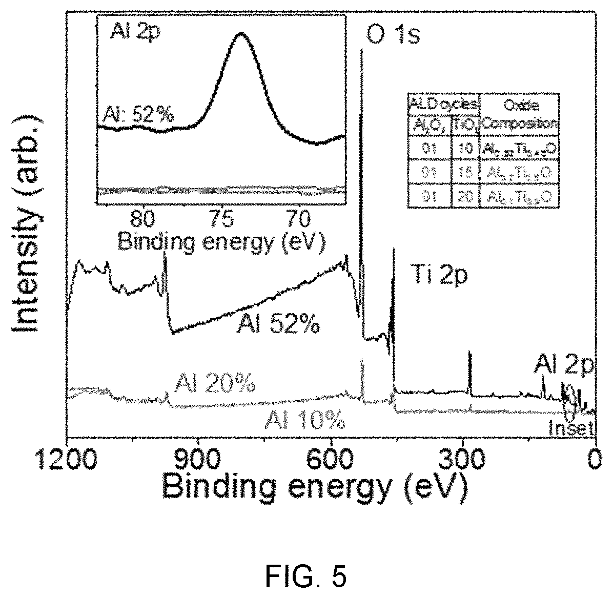
FIG. 5 illustrates XPS spectra of ALD grown AlTiO validating incorporation of Al in TiO.sub.2, represented by presence of Al (2p) peak.
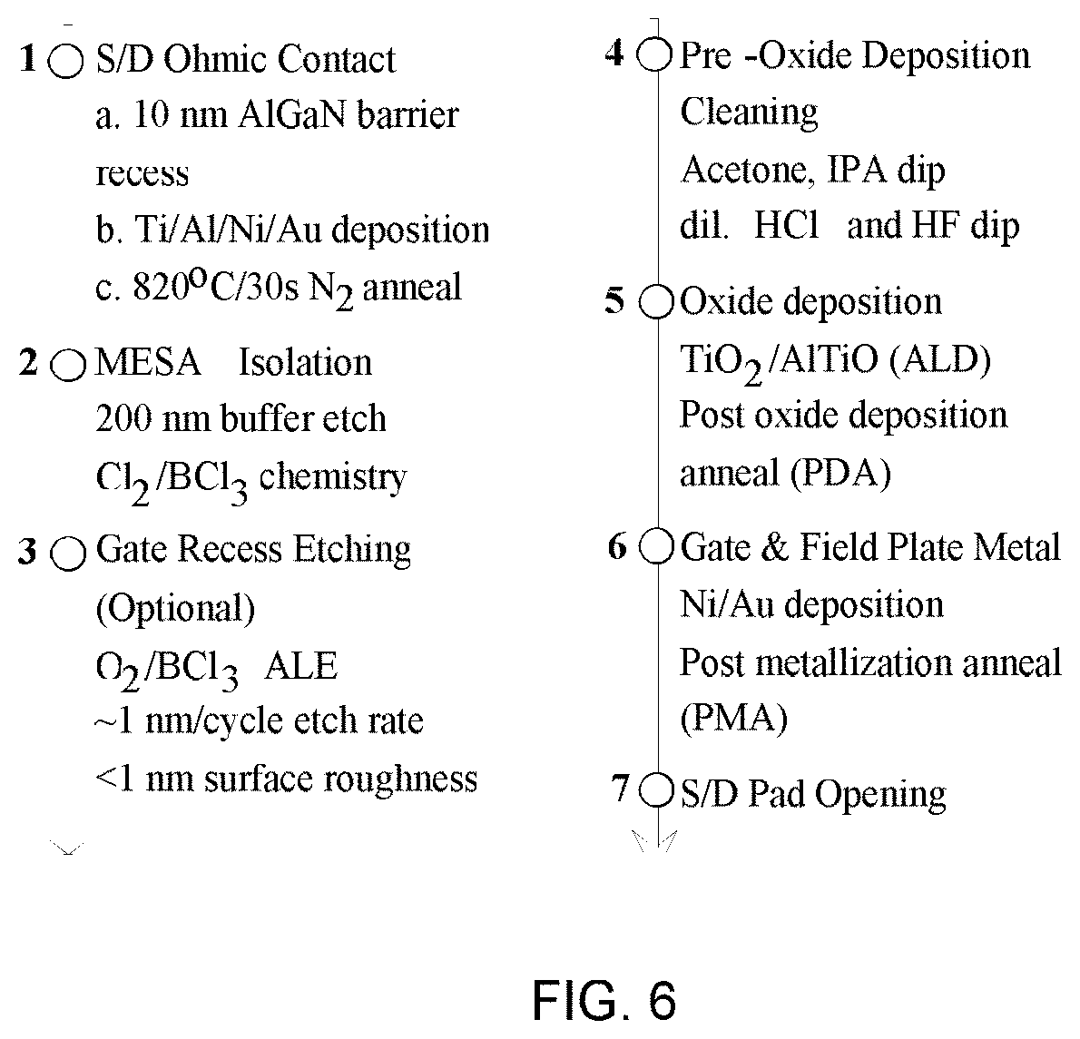
FIG. 6 illustrates fabrication procedure adopted for demonstrating AlGaN/GaN HEMTs designed for e-mode operation with the proposed AlTiO based gate stack.
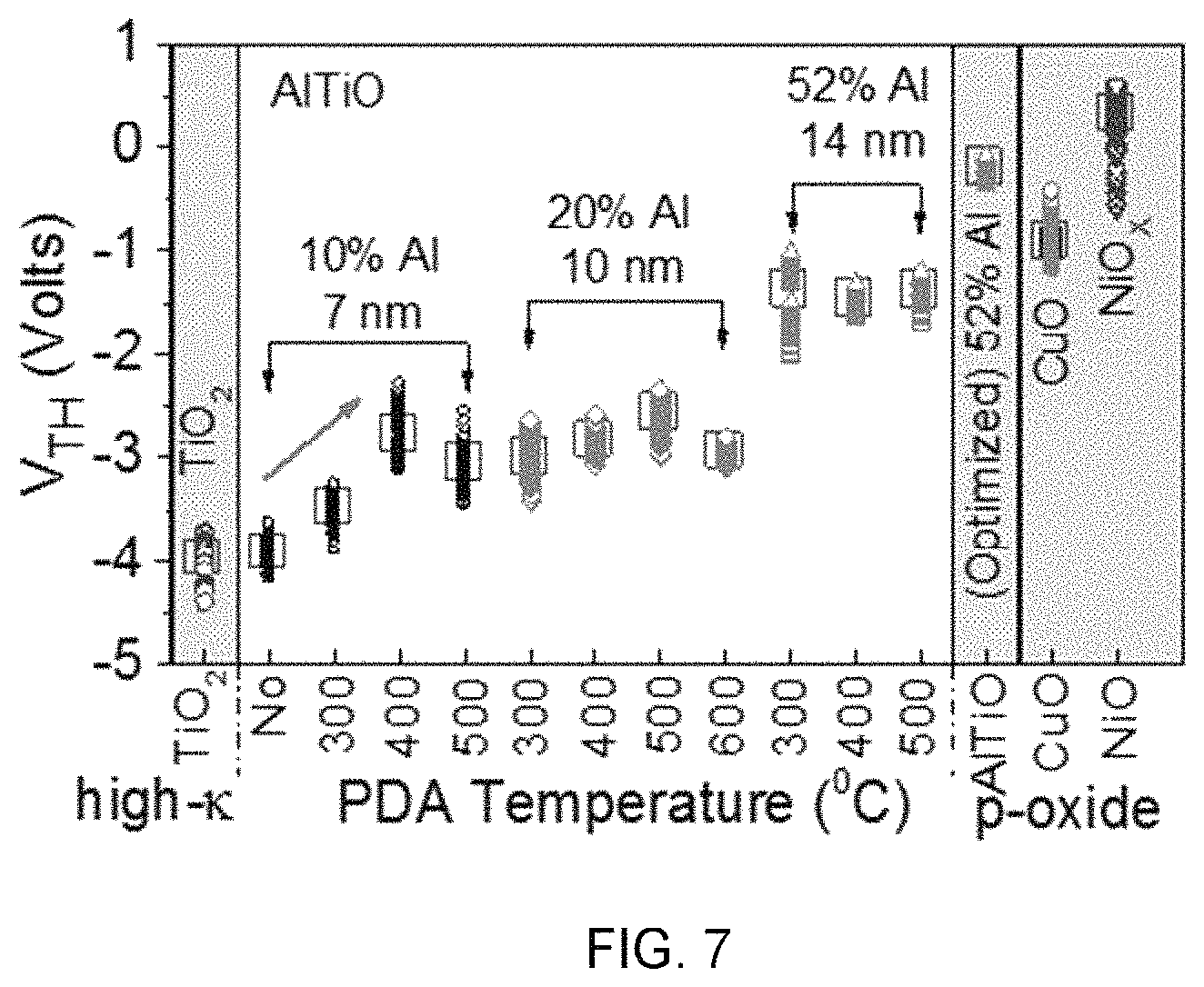
FIG. 7 illustrates threshold voltage as a function of PDA temperatures, Al % and oxide thickness.
FIG. 8 illustrates transfer characteristics of AlTiO and TiO.sub.2 based HEMTs depicting positive shift in V.sub.TH.
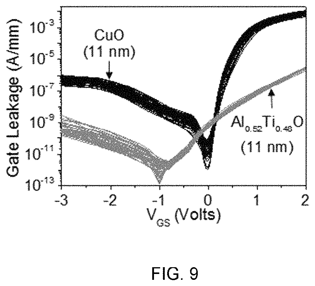
FIG. 9 illustrates gate leakage in AlTiO and CuO based HEMTs.
FIG. 10 illustrates transfer characteristics of AlTiO and TiO.sub.2 based HEMTs depicting improvement in subthreshold slope.
FIGS. 11A and 11B illustrate accumulation capacitance of AlTiO and TiO.sub.2 based HEMTs and relative dielectric constant of the oxides extracted from respective accumulation capacitances respectively.
FIGS. 12A-12C illustrate energy band diagrams, shift of Fermi energy level away from conduction band in the channel and resulting shift in threshold voltage respectively, as a function of AlGaN barrier thickness under the gate and energy difference between oxide's Fermi level and valence band.
FIG. 13A illustrates I.sub.DS-V.sub.GS characteristics of HEMTs realized using optimized p-oxide with different t.sub.barrier.
FIG. 13B illustrates linear shift in V.sub.TH from negative to positive observed when barrier thickness under the gate is scaled.
FIG. 14 illustrates improvement in OFF state leakage and subthreshold slope (SS), beside V.sub.TH shift, for reduced t.sub.barrier.
FIG. 15 illustrates dual sweep I.sub.DS-V.sub.GS characteristic of the p-type oxide-based e-mode HEMTs with reduced barrier thickness under gate.
FIG. 16 illustrates I.sub.DS-V.sub.GS characteristics of the p-type based e-mode HEMTs depicting superior ON-current and ON-resistance performance.
FIG. 17 illustrates OFF state three terminal breakdown characteristic of the proposed device.
FIG. 18 illustrates increased SOA boundary observed for HEMTs with thinner AlGaN barrier under gate.
FIG. 19 illustrates a cross-sectional view of an HEMT with a hybrid p-type oxide and p-GaN based gate stack.
FIG. 20A illustrates state of the art of AlGaN/GaN e-mode HEMTs reported ON-state performance, compared for various techniques to achieve the e-mode operation.
FIG. 20B illustrates R.sub.ON-V.sub.BD performance of the proposed e-mode devices, compared to the reported works till date.
DETAILED DESCRIPTION
The following is a detailed description of embodiments of the disclosure depicted in the accompanying drawings. The embodiments are in such detail as to clearly communicate the disclosure. However, the amount of detail offered is not intended to limit the anticipated variations of embodiments; on the contrary, the intention is to cover all modifications, equivalents, and alternatives falling within the spirit and scope of the present disclosure as defined by the appended claims.
Various terms as used herein are shown below. To the extent a term used in a claim is not defined below, it should be given the broadest definition persons in the pertinent art have given that term as reflected in printed publications and issued patents at the time of filing.
The present disclosure relates generally to the field of field effect transistors (FET). In particular, the present disclosure relates to gate engineering in High Electron Mobility Transistors (HEMT) for improved enhancement mode performance.
It is an object of the present disclosure to solve technical problems as recited above in the background section. Accordingly, in an embodiment, in order to overcome limitations in prior art described above, and to overcome other limitations that will become apparent upon reading and understanding the present disclosure, the present disclosure provides a novel enhancement mode High Electron Mobility Transistor (HEMT) structure with Al.sub.xTi.sub.1-xO layer (gate oxide) as replacement of p-GaN Gate.
Under the gate, this transistor has an Al.sub.xTi.sub.1-xO epilayer structure, which structure in HEMT enables achievement of threshold voltage tuning from negative to positive by changing p-doping composition. Further, using a proposed p-type oxide (Al.sub.xTi.sub.1-xO epilayer structure in HEMT), a record high performance 600V class of e-mode HEMT device can be achieved with ON current .about.400 mA/mm, a sub-threshold slope of 73 mV/dec, R.sub.on=8.90.OMEGA.mm, interface trap density <10.sup.10 mm.sup.-2eV.sup.-1, and gate leakage below 200 nA/mm at the OFF-state breakdown.
In an aspect, under access and contact regions, epilayer is AlGaN/GaN. Due to spontaneous and piezoelectric polarisation, 2DEG is formed at the AlGaN/GaN interface, and due to the high mobility of the electrons in the 2DEG, ON resistance is low. In another aspect, complete recessing of the AlGaN barrier to achieve e-mode HEMT results in electron mobility degradation due to plasma damage, thereby increasing ON resistance. However, a high positive threshold voltage without ON resistance increment is desirable for e-mode operation. In an embodiment, the present disclosure proposes to use a p-type gate oxide to deplete channel to achieve e-mode operation without any adverse effects of plasma damage or losing channel control.
An aspect of the present disclosure provides a method for fabricating a field effect transistor with a hybrid gate stack that combines p-GaN technology with the high-k oxide for e-mode operation. In an aspect, an Al.sub.xTi.sub.1-xO high-k gate oxide engineering and HEMT architecture is disclosed that eliminates above discussed issues by providing e-mode operation and records high ON-state performance, while using principle of band engineering. In an aspect, oxide emulating p-type band properties (Al.sub.xTi.sub.1-xO high-k gate) can be used as a replacement of p-GaN gate for e-mode HEMT operation.
In an aspect, Al.sub.2O.sub.3, widely used as a gate oxide, has a wider band gap (E.sub.g, about 6.5 eV), a high crystallisation temperature (about 900.degree. C.) and an offset of about 2-2.25 eV with the conduction band of GaN (E.sub.c). It, however, has a low dielectric constant (k, about 9).
In another aspect, TiO.sub.2 has the advantage of having a high k (about 60), though it suffers from a lower Eg (about 3.4 eV), a lower crystallisation temperature (about 370.degree. C.) and a low offset with GaN E.sub.c (about 0.3 eV).
In another aspect, a ternary oxide system of Al--Ti--O, by introducing Al.sub.2O.sub.3 in TiO.sub.2 can have improved band offset with GaN E.sub.c, a higher crystallisation temperature, while maintaining a high k.
In an aspect, Al behaves as a negative fixed charge in TiO.sub.2, introducing holes in the system and making Al--Ti--O a p-type oxide.
FIG. 1A reveals an Eg of 3.35 eV and a Fermi energy (E.sub.F) to oxide valence band energy (E.sub.V, P-OXIDE) difference .DELTA.E.sub.V, P-OXIDE (=E.sub.F-E.sub.V, P-OXIDE) of about 0.56 eV for TiO.sub.2.
FIG. 1B depicts DFT calculations for Al in TiO.sub.2 system, showing that introduction of Al in TiO.sub.2 systematically lowers .DELTA.E.sub.V, P-OXIDE offering Al as a knob to control p-type behaviour in the proposed ternary oxide system.
It is known that 2DEG present in HEMT structure originates from Fermi level positioned above the conduction band, and therefore tuning the position of Fermi level can enhance or deplete the 2DEG. For conventional high-k oxides such as Al.sub.2O.sub.3 and TiO.sub.2, Fermi level in the channel region is always above the conduction band, making the device normally-ON. Accordingly, in an embodiment of the present disclosure, an oxide that can emulate p-type nature by positioning valance band above the Fermi level leading to a negative Fermi energy to valance band energy difference (.DELTA.E.sub.v=E.sub.F-E.sub.v) is used as a control parameter to deplete the 2DEG in channel.
In an embodiment, a HEMT device as shown in FIG. 2A with a gate oxide having Fermi energy close to valance band energy is analysed using TCAD simulations. FIG. 2A illustrates a cross sectional view of the HEMT with p-type gate oxide proposed for e-Mode operation, in accordance with an embodiment of the present disclosure.
In another embodiment, when a p-type oxide is used inside a HEMT gate stack, as show in in FIG. 2B, E.sub.F in the channel gets shifted away from the conduction band edge (E.sub.c). FIGS. 3A and 3B illustrate the shifting of E.sub.F in the channel away from E.sub.c when a conventional oxide and p-type gate oxide is used in an HEMT stack respectively.
In another embodiment, detailed TCAD simulations along with DFT reveal that the Fermi energy level in the channel shifts below the conduction band energy level (E.sub.c,2DEG>0) when the oxide's Fermi energy to valance band energy gap (.DELTA.E.sub.V, P-OXIDE) is reduced below 0.2 eV, as illustrated in FIG. 4A. Furthermore, a shift in .DELTA.E.sub.C,2DEG was found to increase with the thickness of p-oxide, as illustrated in FIG. 4B.
In another embodiment, depletion of electrons in the 2DEG under the p-oxide gate stack for .DELTA.E.sub.C,2DEG>0 resulted in a positive shift in V.sub.TH, which can be controlled by .DELTA.E.sub.V,P-Oxide (Al %) and p-oxide thickness, as illustrated in FIG. 4C.
In an aspect, the percentage of Al in the AlTiO can be used as a parameter to control V.sub.TH of AlGaN/GaN HEMTs. In an exemplary embodiment, it can be observed that an active Al composition of about 1-2% can result in the required threshold voltage shift. However, the Al % for p-type behaviour is found to vary experimentally, and this behaviour can be attributed to the amorphous nature and the growth dependent stoichiometry of the developed ALD oxide.
In an embodiment, the present disclosure proposes to include Al atoms in TiO.sub.2 in order to impart p-type behaviour to oxide, which can be achieved using Atomic Layer Deposition (ALD) using sequential cycles of Al.sub.2O.sub.3 and TiO.sub.2 deposition. Alternate cycles of trimethylaluminium (TMA) and H.sub.2O precursors were used to deposit Al.sub.2O.sub.3 in an ALD chamber at 250.degree. C. In between each of these Al.sub.2O.sub.3 cycles, TiO.sub.2 can be deposited at 250.degree. C. using Titanium tetraisopropoxide (TTIP) and H.sub.2O, with variation in the number of cycles to obtain varied Al composition (10%, 20% and 52%) in the ternary oxide Al.sub.xTi.sub.1-xO. FIG. 5 illustrates an XPS spectra for various TiO.sub.2 and Al.sub.2O.sub.3 deposition cycles used to control metal concentrations in the Al.sub.xTi.sub.1-xO system (inset Table 1). In an exemplary embodiment, more than a 100 post oxide deposition anneal (PDA) and post gate metallization anneal (PMA) splits were carried out to optimize the ternary oxide system.
In another embodiment, fabrication of HEMT with Al.sub.xTi.sub.1-xO dielectric can be performed as elaborated in FIG. 6, on AlGaN/GaN stack, which can be grown using Metal-Organic Chemical Vapour Deposition (MOCVD) technique on Si substrate. 22 nm AlGaN can be grown on GaN buffer separated by a 1 nm AlN spacer and capped by 3 nm GaN. Transistors can be fabricated on the stack starting with 870.degree. C. N.sub.2 annealed Ti/Al/Ni/Au for ohmic contacts followed by MESA isolation using Cl.sub.2/BCl.sub.3 chemistry. Ni/Au Schottky gate contact can finally be established, post blanket dielectric deposition, followed by a low temperature anneal. In a further embodiment, for devices with reduced barrier thickness under the gate, O.sub.2--BCl.sub.3 atomic layer etching (ALE) was used, followed by post plasma surface treatment.
In another embodiment, in order to evaluate the HEMT with the proposed AlTiO oxide, other HEMTs with high-k TiO.sub.2 and p-oxides like CuO and NiO.sub.x were also realized over the same epi stack. HEMTs with TiO.sub.2 resulted in depletion mode (d-mode) operation with a deep-seated V.sub.TH of about -4V. FIG. 7 illustrates a permanent shift in HEMT threshold voltage when AlTiO is used in the gate stack. An increase in PDA temperature for an optimized PMA results in a systematic shift in V.sub.TH, which can be attributed to changes in Al activation % in AlTiO as a function of PDA time and temperature.
FIG. 8 illustrates a permanent shift in HEMT threshold voltage when AlTiO is used in the gate stack. A shift in V.sub.TH of about 0.7V is observed for 10% Al, whereas for AlTiO with about 52% Al, a shift of about 3.8V is seen. This validates the role of Al % as a control knob to tune V.sub.TH.
Referring again to FIG. 9, it can be seen that other p-oxides such as CuO and NiO.sub.x based HEMTs can also offer positive V.sub.TH shift. However, their performance can be claimed inferior to that of AlTiO for the following reasons: CuO offers a lower V.sub.TH shift when compared to AlTiO; CuO as gate oxide results in a .about.4 order (.about.2 order) higher leakage current under accumulation (inversion) condition when compared to AlTiO for the same thickness, as illustrated in FIG. 10; and NiO.sub.x based HEMTs suffer from very high gate leakage compared to AlTiO and CuO with large variability (data not shown).
In another embodiment, the advantage of AlTiO system over other p-oxides can be seen further from the improvement in subthreshold slope (SS) of about 10 mV/dec compared to the TiO.sub.2 counterpart, as illustrated in FIG. 10. In an exemplary embodiment, FIGS. 11A and 11B illustrate an optimized high-k proposed oxide Al.sub.0.52Ti.sub.0.48O, with a dielectric constant of about 25.
It may be appreciated that the right shift in the V.sub.th using Al.sub.xTi.sub.1-xO dielectric is critical for designing a normally OFF HEMT device. The .DELTA.E.sub.c,2DEG can be increased further so as to completely deplete the 2DEG. In an exemplary embodiment, one way is to increase oxide thickness to provide additional shift to conduction band until it turns the channel OFF. However, the thick dielectric gate leads to weaker channel control, which can result in a higher source to drain leakage current besides negating the advantages of ultra-thin dielectric.
In another embodiment, the simulations also predict depletion of the 2DEG for higher p-type behaviour in oxide. For HEMTs with oxides such as Al.sub.2O.sub.3 or TiO.sub.2, to make a normally OFF device, full recessed gate can be employed. It however can have variability issues, wherein damage to channel in this process may have detrimental effects on 2DEG and hence on-state performance.
In another embodiment, to mitigate issues as presented above, the effectiveness of the p-oxide gate can be increased by bringing the gate stack closer to the channel by the partial removal of the AlGaN barrier under the gate before depositing the p-oxide, as illustrated in FIGS. 12A-12C. FIGS. 12A-12C illustrate the energy band diagrams, shift of Fermi Energy level away from the conduction band in the channel and the resulting shift in threshold voltage respectively, as a function of AlGaN barrier thickness under the gate for a constant thickness of p-oxide under the gate (about 60 nm).
In another embodiment, the experimental results, as presented in FIG. 13A illustrates a shift in V.sub.TH from -0.2V to 0.5V by reducing the barrier thickness under the gate from 22 nm to 8 nm. FIG. 13B illustrates a linear shift in V.sub.TH observed when the barrier thickness under the gate is scaled. It can be appreciated here, that the channel is still 8 nm away from the oxide-semiconductor interface, which helps in mitigating the detrimental effects of plasma damage on 2DEG induced during the ALE of AlGaN. Referring to FIG. 13A again, it can be seen that reducing barrier thickness (t.sub.barrier=8 nm) under the gate in conjunction with 11 nm p-type AlTiO resulted in e-mode GaN HEMT.
FIG. 14 illustrates, for a HEMT with thinner AlGaN barrier, an improved channel control, which further results in a lower OFF-state leakage and an improved SS. The OFF-state leakage was found to reduce by 100.times., whereas SS for e-mode HEMT was found to improve from 101 mV/dec to 73 mV/dec when t.sub.barrier was scaled from 22 nm to 8 nm.
FIG. 15 illustrates a low V.sub.TH hysteresis of about 40 mV during I.sub.DS-V.sub.GS dual sweep. The low hysteresis is attributed to the fact that the channel is 8 nm away from the oxide-GaN interface.
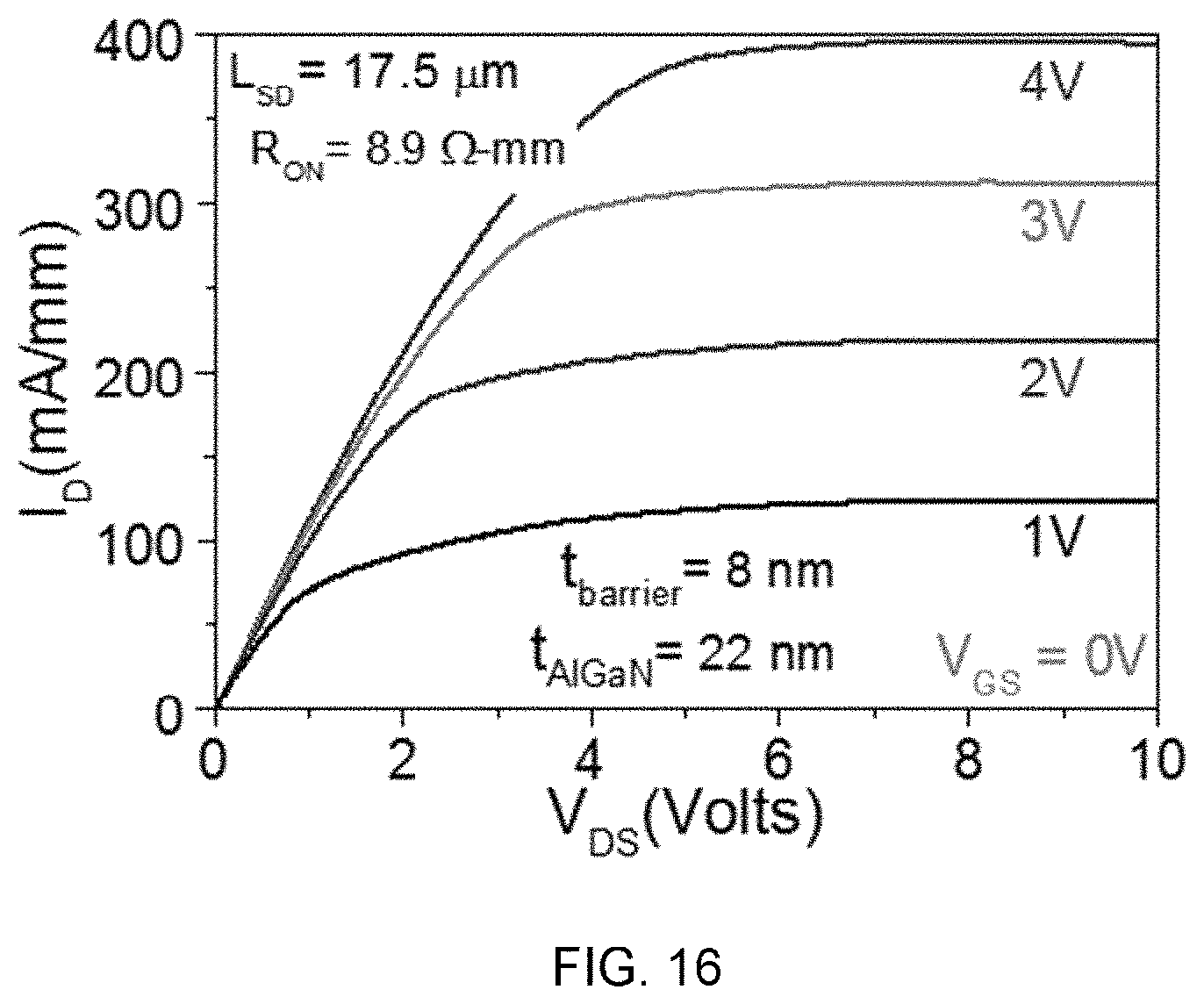
FIG. 16 illustrates a superior ON-state performance of the e-mode HEMTs, with a drain current of about 400 mA/mm at V.sub.GS=4V, R.sub.ON=8.9 .OMEGA.-mm and I.sub.ON/I.sub.OFF=10.sup.7.
FIG. 17 depicts three terminal breakdown voltage (substrate grounded) >600V; sub-nA source-drain leakage and OFF-state gate leakage under high drain stress conditions highlight the usability of these devices.
FIG. 18 illustrates an improved safe operating area (SOA) reliability due to reducing the AlGaN barrier thickness under the gate stack.
FIG. 19 illustrates an HEMT architecture with a hybrid gate stack comprising the proposed p-type oxide and p-GaN, in an exemplary embodiment of the present disclosure. In an embodiment, the hybrid gate stack offers a means to lower p-GaN doping while maintaining e-mode operation using the proposed Al--Ti--O based gate engineering.
FIG. 20A illustrates the state-of-the-art AlGaN/GaN e-mode HEMTs reported ON-state performance compared for various techniques to achieve e-mode operation. FIG. 20B illustrates R.sub.ON-V.sub.BD performance of the proposed e-mode device when compared to other reported works. The three terminal breakdown voltage is measured for an OFF-state source-drain leakage of 1 .mu.A/mm.
In summary, it can be seen that Al.sub.xTi.sub.1-xO exhibits p-type behaviour, and when integrated in a HEMT gate stack, results in a positive threshold voltage shift where Al % can be used to tune the V.sub.TH. The proposed oxide can be seen to have advantages over other p-type oxides such as CuO and NiO.sub.x in terms of gate leakage and variability. Using the proposed p-type oxide, e-mode HEMTs are demonstrated with a V.sub.TH of about 0.5V and very low hysteresis. It is also seen that a thinner barrier and high-k nature of AlTiO results in superior gate control over channel and ON state performance.
While the foregoing describes various embodiments of the invention, other and further embodiments of the invention may be devised without departing from the basic scope thereof. The scope of the invention is determined by the claims that follow. The invention is not limited to the described embodiments, versions or examples, which are included to enable a person having ordinary skill in the art to make and use the invention when combined with information and knowledge available to the person having ordinary skill in the art.
ADVANTAGES
The present disclosure provides a field effect transistor (FET) operating in enhancement mode (e-mode).
The present disclosure provides an FET with a tunable threshold voltage.
The present disclosure provides an FET with a gate oxide which emulates p-type behaviour.
* * * * *
D00000
D00001
D00002
D00003
D00004
D00005
D00006
D00007
D00008
D00009
D00010
D00011
D00012

D00013

D00014

D00015

D00016
D00017

D00018

D00019

D00020

XML
uspto.report is an independent third-party trademark research tool that is not affiliated, endorsed, or sponsored by the United States Patent and Trademark Office (USPTO) or any other governmental organization. The information provided by uspto.report is based on publicly available data at the time of writing and is intended for informational purposes only.
While we strive to provide accurate and up-to-date information, we do not guarantee the accuracy, completeness, reliability, or suitability of the information displayed on this site. The use of this site is at your own risk. Any reliance you place on such information is therefore strictly at your own risk.
All official trademark data, including owner information, should be verified by visiting the official USPTO website at www.uspto.gov. This site is not intended to replace professional legal advice and should not be used as a substitute for consulting with a legal professional who is knowledgeable about trademark law.