Implementing backdrilling elimination utilizing anti-electroplate coating
Doyle , et al. October 6, 2
U.S. patent number 10,798,829 [Application Number 15/821,042] was granted by the patent office on 2020-10-06 for implementing backdrilling elimination utilizing anti-electroplate coating. This patent grant is currently assigned to International Business Machines Corporation. The grantee listed for this patent is International Business Machines Corporation. Invention is credited to Matthew S. Doyle, Joseph Kuczynski, Phillip V. Mann, Kevin M. O'Connell.

| United States Patent | 10,798,829 |
| Doyle , et al. | October 6, 2020 |
Implementing backdrilling elimination utilizing anti-electroplate coating
Abstract
A method and structure are provided for implementing enhanced via creation without creating a via barrel stub. The need to backdrill vias during printed circuit board (PCB) manufacturing is eliminated. After the vias have been drilled, but before plating, a plug is inserted into each via and the plug is lowered to a depth just below a desired signal trace layer. A thin anti-electroplate coating is applied onto the walls of the via below the signal trace. Then the plugs are removed and a standard board plating process for the PCB is performed.
| Inventors: | Doyle; Matthew S. (Chatfield, MN), Kuczynski; Joseph (North Port, FL), Mann; Phillip V. (Rochester, MN), O'Connell; Kevin M. (Rochester, MN) | ||||||||||
|---|---|---|---|---|---|---|---|---|---|---|---|
| Applicant: |
|
||||||||||
| Assignee: | International Business Machines
Corporation (Armonk, NY) |
||||||||||
| Family ID: | 1000005100303 | ||||||||||
| Appl. No.: | 15/821,042 | ||||||||||
| Filed: | November 22, 2017 |
Prior Publication Data
| Document Identifier | Publication Date | |
|---|---|---|
| US 20180098438 A1 | Apr 5, 2018 | |
Related U.S. Patent Documents
| Application Number | Filing Date | Patent Number | Issue Date | ||
|---|---|---|---|---|---|
| 15217019 | Jul 22, 2016 | 9872399 | |||
| Current U.S. Class: | 1/1 |
| Current CPC Class: | H05K 1/115 (20130101); H05K 3/425 (20130101); H05K 3/423 (20130101); H05K 1/034 (20130101); H05K 2203/143 (20130101); H05K 2201/015 (20130101) |
| Current International Class: | H05K 1/02 (20060101); H05K 3/40 (20060101); H05K 1/03 (20060101); H05K 1/11 (20060101); H05K 3/00 (20060101); H05K 3/42 (20060101); H01L 21/311 (20060101); H01L 23/48 (20060101) |
| Field of Search: | ;174/258,255,260,264,266,257,262 ;29/745,852,846 ;438/700 ;428/137,209 |
References Cited [Referenced By]
U.S. Patent Documents
| 4010321 | March 1977 | Kohashi |
| 4510347 | April 1985 | Wiech, Jr. |
| 4603372 | July 1986 | Abadie |
| 4675694 | June 1987 | Bupara |
| 5082730 | January 1992 | Takeda |
| 5114904 | May 1992 | Kawakami |
| 5184478 | February 1993 | Kutsuna |
| 5206084 | April 1993 | Takeda |
| 5227285 | July 1993 | Hattori |
| 5326686 | July 1994 | Katoh |
| 5766821 | June 1998 | Muramatsu |
| 5798559 | August 1998 | Bothra et al. |
| 5879851 | March 1999 | Takahashi |
| 5891598 | April 1999 | Miyabe |
| 6147249 | November 2000 | Watanabe et al. |
| 6280898 | August 2001 | Hasegawa et al. |
| 6284429 | September 2001 | Kinsho et al. |
| 6399274 | June 2002 | Kinsho et al. |
| 6420085 | July 2002 | Nishi et al. |
| 6458696 | October 2002 | Gross |
| 6524765 | February 2003 | Nishi et al. |
| 6511783 | June 2003 | Uenishi |
| 6667145 | December 2003 | Nishi et al. |
| 6673512 | January 2004 | Uenishi et al. |
| 6703131 | March 2004 | Kayanoki |
| 6887646 | May 2005 | Fujiwara et al. |
| 7586047 | September 2009 | Hayashi et al. |
| 7794799 | September 2010 | Kim |
| 8815215 | August 2014 | Prencipe |
| 9781830 | October 2017 | Iketani |
| 2001/0055726 | December 2001 | Kanna et al. |
| 2002/0058179 | May 2002 | Segit |
| 2002/0136980 | September 2002 | Sasaki et al. |
| 2003/0049913 | March 2003 | Gaku et al. |
| 2003/0054287 | March 2003 | Yasunami et al. |
| 2003/0075708 | April 2003 | Kodama |
| 2003/0165776 | September 2003 | Yasunami et al. |
| 2003/0167793 | September 2003 | Honda |
| 2003/0186537 | October 2003 | Yamanaka et al. |
| 2003/0190543 | October 2003 | Sugiura |
| 2003/0198894 | October 2003 | Mizutani et al. |
| 2003/0203305 | October 2003 | Yasunami et al. |
| 2004/0033438 | February 2004 | Hamada et al. |
| 2004/0218917 | November 2004 | Mizutani |
| 2005/0014092 | January 2005 | Hasegawa et al. |
| 2005/0038261 | February 2005 | Maewawa et al. |
| 2005/0079420 | April 2005 | Cho |
| 2005/0117251 | June 2005 | Matono et al. |
| 2006/0003252 | January 2006 | Hirayama et al. |
| 2006/0127652 | June 2006 | Kanaya et al. |
| 2006/0199390 | September 2006 | Dudnikov, Jr. |
| 2007/0184254 | August 2007 | Matsuno |
| 2008/0029855 | February 2008 | Chang |
| 2008/0220354 | September 2008 | Miyakawa |
| 2008/0227000 | September 2008 | Honda |
| 2008/0241745 | October 2008 | Shirakawa et al. |
| 2008/0296057 | December 2008 | Dudnikov, Jr. |
| 2009/0035585 | February 2009 | Wakaki |
| 2009/0053632 | February 2009 | Ishii |
| 2009/0169806 | July 2009 | Lo |
| 2009/0173532 | July 2009 | Sugane |
| 2010/0044095 | February 2010 | Kuczynski |
| 2010/0044096 | February 2010 | Kuczynski |
| 2010/0126009 | May 2010 | Li et al. |
| 2010/0181559 | July 2010 | Nakatani |
| 2010/0222196 | September 2010 | Ito |
| 2012/0160556 | June 2012 | Kim et al. |
| 2012/0181251 | July 2012 | Minegishi et al. |
| 2012/0234587 | September 2012 | Nakamura |
| 2012/0236523 | September 2012 | Yasuo et al. |
| 2013/0029141 | January 2013 | Tanaka |
| 2013/0092617 | April 2013 | Kashihara |
| 2013/0092618 | April 2013 | Kashihara |
| 2013/0277097 | October 2013 | Maeng |
| 2013/0341073 | December 2013 | Hsu et al. |
| 2014/0011949 | January 2014 | Asami |
| 2014/0014401 | January 2014 | Liao et al. |
| 2014/0047728 | February 2014 | Shinada |
| 2014/0163124 | June 2014 | Kurashina |
| 2014/0190733 | July 2014 | Dudnikov, Jr. |
| 2014/0220783 | August 2014 | Koumura et al. |
| 2014/0251663 | September 2014 | Iketani |
| 2014/0262455 | September 2014 | Iketani |
| 2014/0335028 | November 2014 | Prencipe |
| 2015/0021069 | January 2015 | Chiu et al. |
| 2015/0147565 | May 2015 | Popovici |
| 2015/0181724 | June 2015 | Iketani |
| 2016/0021762 | January 2016 | Kallman |
| 2016/0278207 | September 2016 | Pen |
| 2016/0278208 | September 2016 | Pen |
| 2016/0360624 | December 2016 | Kuwako |
| 2016/0372276 | December 2016 | Han et al. |
| 2017/0048974 | February 2017 | Shiina |
| 10510706394 | Nov 2015 | CN | |||
| 105200473 | Dec 2015 | CN | |||
| 105338758 | Feb 2016 | CN | |||
Other References
|
Appendix P List of Patents and Patent Applications Treated as Related Jan. 24, 2018. cited by applicant . PTFE Deposition: View by MNX MEMS & Nanotechnology Exchange, https://www.mems-exchange.org/catalog/P33T2/ 2016. cited by applicant. |
Primary Examiner: Chen; Xiaoliang
Attorney, Agent or Firm: Rau; Nathan M.
Parent Case Text
This application is a continuation application of Ser. No. 15/217,019 filed Jul. 22, 2016.
Claims
What is claimed is:
1. A structure for implementing enhanced via creation during printed circuit board (PCB) manufacturing comprising: a printed circuit board (PCB); said printed circuit board (PCB) having an internal conductive signal trace; a single through hole defining a via formed by via drilling, said via having a single uniform diameter extending through the printed circuit board (PCB) and said via extending through the internal conductive signal trace; an anti-electroplate coating covering the walls of said via spaced below the internal conductive signal trace; said anti-electroplate coating formed of a chemically resistant polymer; said anti-electroplate coating chemically resistant polymer having a selected thickness of approximately 0.2 .mu.m; a via plating formed on walls of said via, said via plating extending above said anti-electroplate coating on walls of said via and extending on walls of said via through and below the internal conductive signal trace; said via plating electrically connected to the internal conductive signal trace; and said anti-electroplate coating preventing via plating from taking hold in the structure on the walls of said via spaced below the internal conductive signal trace, eliminating via barrel stub creation during PCB manufacturing; wherein said anti-electroplate coating is applied below a plug in said via, said plug used during printed circuit board (PCB) manufacturing.
2. The structure as recited in claim 1, wherein said anti-electroplate coating includes a hydrophobic polymer applied by vapor deposition.
3. The structure as recited in claim 1, wherein said PCB manufacturing PCB includes forming said via coating applied by conventional plating processes being performed after forming said anti-electroplate coating.
4. The structure as recited in claim 1, wherein said anti-electroplate coating includes a hydrophobic polymer applied by vapor deposition.
5. The structure of claim 1, wherein said anti-electroplate coating includes a polytetrafluoroethylene (PTFE) coating applied by vapor deposition.
Description
FIELD OF THE INVENTION
The present invention relates generally to the data processing field, and more particularly, relates to a method and structure for implementing manufacture of a printed circuit board (PCB) with enhanced via creation without creating a via barrel stub, eliminating the need to back-drill.
DESCRIPTION OF THE RELATED ART
The computer hardware development industry has reached a point wherein many computer interfaces are of sufficient switching speed as to require signal routing layer change vias to be back-drilled to remove via barrel stubs. Backdrilling is a conventional technique used to remove the via barrel stub. Without removal of the unnecessary section or length of a via barrel, some amount of the propagating signal is reflected away from the intended receiver, thereby significantly reducing the amount of total energy effectively transferred from driver to receiver.
While there are known processes to mechanically remove these stubs, once back-drilled, it is no longer possible to probe those locations on the printed circuit board (PCB), cost of the PCB increases substantially, and success of the process is statistically less than ideal. These facts significantly complicate our ability to manufacture cost-effective PCBs, measure high-speed interfaces in the lab during system bring-up and model-to-hardware correlation activities, and maximize the electrical performance of our computer interfaces. When system errors occur in the field, the field engineer cannot measure and confirm function at these PCB via locations while at the customer's site.
A need exists for a method and structure for implementing via creation that eliminates creation of a via barrel stub, eliminating the need to back-drill, reducing PCB cost, and maximizing interface margin.
As used in the following description and claims, the term printed circuit board (PCB) should be understood to broadly include a printed wiring board or other substrate, an interconnect substrate, and various substrates including a plurality of insulator layers, and internal conductive traces.
SUMMARY OF THE INVENTION
Principal aspects of the present invention are to provide a method and structure for implementing manufacture of a printed circuit board (PCB) with enhanced via creation without creating a via barrel stub, eliminating the need to back-drill. Other important aspects of the present invention are to provide such method and structure substantially without negative effects and that overcome many of the disadvantages of prior art arrangements.
In brief, a method and structure are provided for implementing enhanced via creation without creating a via barrel stub. The need to backdrill during printed circuit board (PCB) manufacturing is eliminated. After the vias have been drilled, but before plating, a plug is inserted into each via and the plug is lowered to a depth just below a desired signal trace layer. A thin anti-electroplate coating is applied onto the walls of the via below the signal trace. Then the plugs are removed and a board plating process for the PCB is performed.
In accordance with features of the invention, the anti-electroplate coating includes, for example, a Teflon coating or a polytetrafluoroethylene (PTFE) coating, Teflon is a trade name for PTFE.
In accordance with features of the invention, the Teflon coating is applied, for example, using vapor deposition onto the walls of the via below the signal trace.
In accordance with features of the invention, the coating prevents the plating from creating via barrel stubs, thus eliminating the need to backdrill each via after the plating process.
In accordance with features of the invention, eliminating back-drilling improves yield and late fail discoveries, both of which can improve cost and reliability of boards.
BRIEF DESCRIPTION OF THE DRAWINGS
The present invention together with the above and other objects and advantages may best be understood from the following detailed description of the preferred embodiments of the invention illustrated in the drawings, wherein:
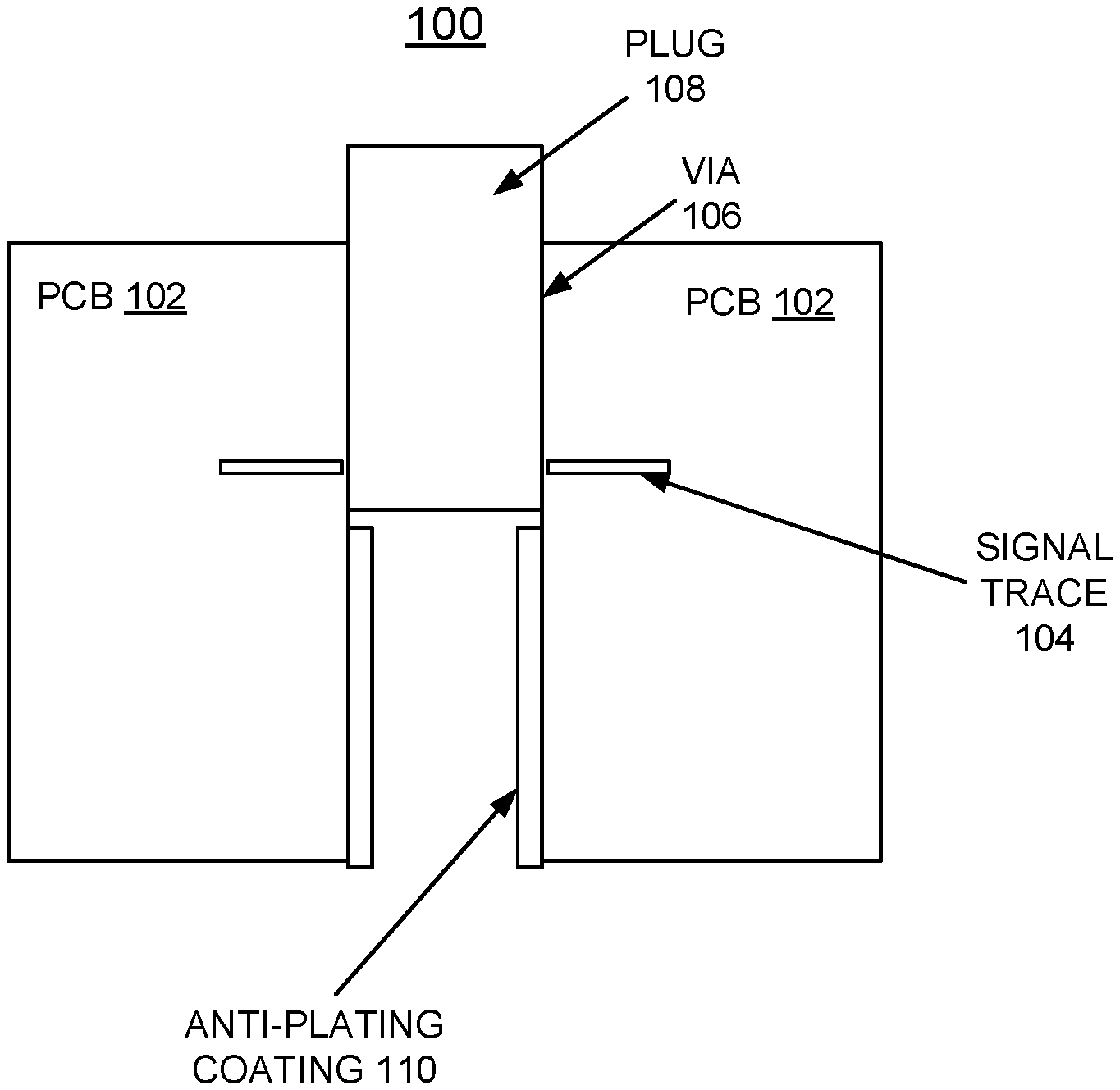
FIG. 1 illustrates an example structure for manufacturing a printed circuit board (PCB) with enhanced via creation without creating a via barrel stub, eliminating the need to back-drill in accordance with the preferred embodiment;
FIG. 2 is a flow chart illustrating example steps for implementing a structure embodying the enhanced via creation without creating a via barrel stub in accordance with the preferred embodiment; and
FIG. 3 illustrates an example structure for manufacturing a printed circuit board (PCB) with enhanced via creation without creating a via barrel stub, eliminating the need to back-drill in accordance with the preferred embodiment.
DETAILED DESCRIPTION OF THE PREFERRED EMBODIMENTS
In the following detailed description of embodiments of the invention, reference is made to the accompanying drawings, which illustrate example embodiments by which the invention may be practiced. It is to be understood that other embodiments may be utilized and structural changes may be made without departing from the scope of the invention.
The terminology used herein is for the purpose of describing particular embodiments only and is not intended to be limiting of the invention. As used herein, the singular forms "a", "an" and "the" are intended to include the plural forms as well, unless the context clearly indicates otherwise. It will be further understood that the terms "comprises" and/or "comprising," when used in this specification, specify the presence of stated features, integers, steps, operations, elements, and/or components, but do not preclude the presence or addition of one or more other features, integers, steps, operations, elements, components, and/or groups thereof.
In accordance with features of the invention, a method and structure are provided for implementing enhanced via creation without creating a via barrel stub. The need to backdrill vias during printed circuit board (PCB) manufacturing is eliminated. After the vias have been drilled, but before plating, a plug is inserted into each via and the plug is lowered to a depth just below a desired signal trace layer. A thin anti-electroplate coating is applied onto the walls of the via below the plug and the signal trace. Then the plugs are removed and a board plating process for the PCB is performed.
Having reference now to the drawings, in FIG. 1, there is shown an example structure generally designated by reference character 100 for manufacturing a printed circuit board (PCB) with enhanced via creation without creating a via barrel stub, eliminating the need to back-drill in accordance with the preferred embodiment.
Structure 100 includes a printed circuit board (PCB) 102 having an internal conductive or signal trace 104. PCB 102 includes an insulator substrate or insulator layers, with one or more internal conductive traces 104. Structure 100 includes a via 106 extending through the printed circuit board (PCB) 102 and the internal conductive trace 104. Structure 100 includes an anti-electroplate coating 110 covering the walls of the via 106 below the signal trace 104. The anti-electroplate coating 110 eliminates via barrel stub creation during a PCB plating process during PCB manufacturing. The anti-electroplate coating 110 is a chemically resistant polymer and is hydrophobic. The anti-electroplate coating 110 has a selected thickness, for example, in a range between 0.2 .mu.m and 0.5 .mu.m.
The anti-electroplate coating 110 includes, for example, a polytetrafluoroethylene (PTFE) coating (e.g., trade name Teflon), that is applied for example, using vapor deposition onto the walls of the via 106 below the signal trace 104.
"PTFE Deposition: View" by MNX MEMS & Nanotechnology Exchange, detailing example vapor deposition of Teflon, is provided at: https://www.mems-exchange.org/catalog/P3372/
The PTFE coating 110 prevents the PCB plating process from creating via barrel stubs, thus eliminating the need to backdrill each via after the plating process. Eliminating back-drilling improves yield and late fail discoveries, both of which can improve cost and reliability of boards.
In accordance with features of the invention, the printed circuit board (PCB) 102 and via 106 are formed generally including standard PCB manufacturing processes, including via drilling and plating. However, the step of back-drilling at the end is removed and the PCB process of the invention provides that after the vias 106 have been drilled, but before plating, a small plug 108 is inserted into each via 106 extending to a defined depth just below the desired signal trace layer 104. A thin coating 110 of Teflon is then applied using vapor deposition onto the walls of the via 106 below the signal trace 104, and then the plugs 108 are removed. The PCB 102 is then sent through the normal plating process. The coating 110 prevents the plating from taking hold, thus eliminating the need to backdrill each via after the plating process.
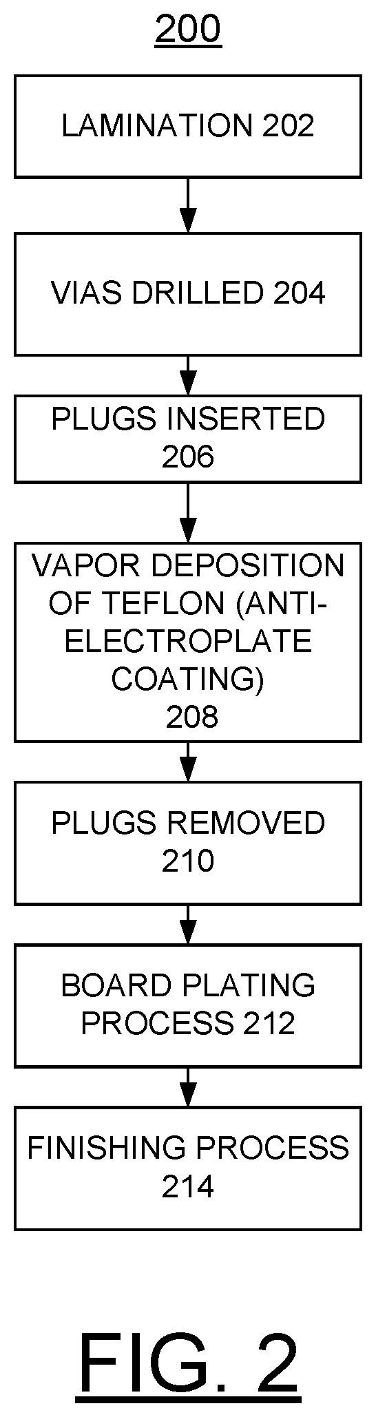
Referring now to FIG. 2, there is shown a flow chart illustrating example steps generally designated by reference character 200 for implementing a structure embodying the enhanced via creation without creating a via barrel stub in accordance with the preferred embodiment starting at a block 202.
As indicated at a block 202, a lamination is formed defining the PCB 102 and at least one internal conductive traces 104.
As indicated at a block 204, vias 106 are drilled. Conventional via drilling is performed.
As indicated at a block 206, the plugs 108 are inserted into the via 106, with the plugs extending from a top or first surface to a depth below the signal trace 104. The plugs 108 optionally are configured as sprayers (like fuel injectors) to apply the Teflon coating applied to the walls of the via 106 below plugs 108. Optionally, individual plugs 108 having a specified length are pushed flush with one side of the PCB 102, then moved or poked out from the other PCB side. Optionally, individual plugs 108 are mechanically inserted to a specific depth, the retracted. Optionally, an array of plugs 108, typically of differing lengths extending from a plate are all inserted at once, the removed.
As indicated at a block 208, the anti-electroplate coating 110 is applied to the walls of the via 106 below plugs 108 and the signal trace 104, for example, by vapor deposition of Teflon.
As indicated at a block 210, the plugs 108 are removed from the vias 106 after the anti-electroplate coating 110 is applied.
As indicated at a block 212, the PCB plating process is performed, using a conventional plating process.
As indicated at a block 214, conventional PCB finishing processes are performed, advantageously eliminating the need to backdrill each via after the plating process.
Referring now to FIG. 3, there is shown an example resulting structure generally designated by reference character 300 resulting from manufacturing a printed circuit board (PCB) with enhanced via creation without creating a via barrel stub, eliminating the need to back-drill in accordance with the preferred embodiment. Structure 300 shows the plugs 108 removed from the vias 106 after the anti-electroplate coating 110 is applied.
Structure 300 includes the printed circuit board (PCB) 102 having the internal conductive or signal trace 104. Structure 100 includes the via 106 extending through the printed circuit board (PCB) 102 and the internal conductive trace 104. Structure 300 includes the anti-electroplate coating 110 covering the walls of the via 106 below the signal trace 104. Structure 300 includes a plating 302 applied during the PCB plating process that is performed using a conventional plating process.
In accordance with features of the invention, the alternative method for via creation eliminates creation of the via barrel stub. Since the via barrel stub is not created, the need to back-drill is eliminated, reducing PCB cost and maximizing interface margin.
While the present invention has been described with reference to the details of the embodiments of the invention shown in the drawing, these details are not intended to limit the scope of the invention as claimed in the appended claims.
* * * * *
References
D00000
D00001
D00002
D00003
XML
uspto.report is an independent third-party trademark research tool that is not affiliated, endorsed, or sponsored by the United States Patent and Trademark Office (USPTO) or any other governmental organization. The information provided by uspto.report is based on publicly available data at the time of writing and is intended for informational purposes only.
While we strive to provide accurate and up-to-date information, we do not guarantee the accuracy, completeness, reliability, or suitability of the information displayed on this site. The use of this site is at your own risk. Any reliance you place on such information is therefore strictly at your own risk.
All official trademark data, including owner information, should be verified by visiting the official USPTO website at www.uspto.gov. This site is not intended to replace professional legal advice and should not be used as a substitute for consulting with a legal professional who is knowledgeable about trademark law.