Switch circuit and method of switching radio frequency signals
Burgener , et al. September 29, 2
U.S. patent number 10,790,820 [Application Number 16/679,760] was granted by the patent office on 2020-09-29 for switch circuit and method of switching radio frequency signals. This patent grant is currently assigned to pSemi Corporation. The grantee listed for this patent is pSemi Corporation. Invention is credited to Robert H. Benton, Mark L. Burgener, James S. Cable.


View All Diagrams
| United States Patent | 10,790,820 |
| Burgener , et al. | September 29, 2020 |
Switch circuit and method of switching radio frequency signals
Abstract
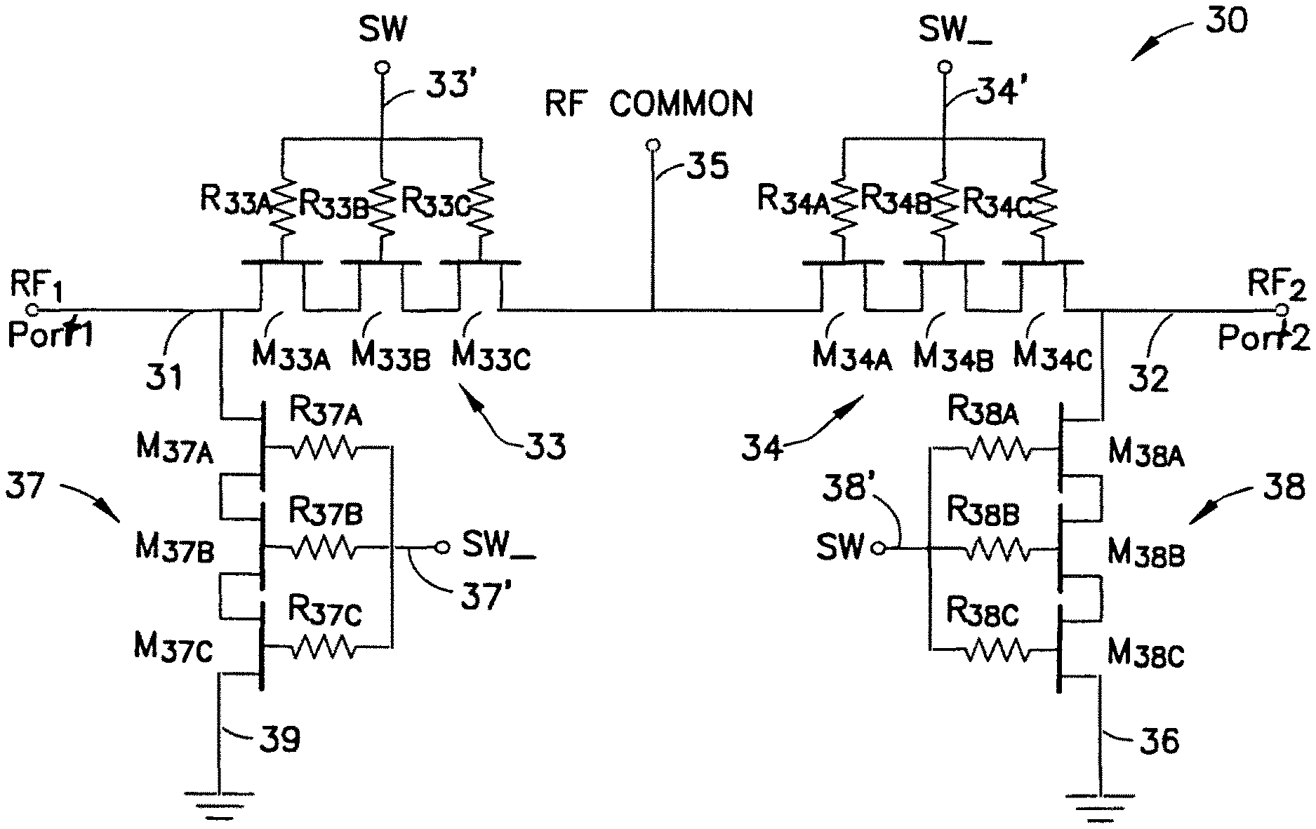
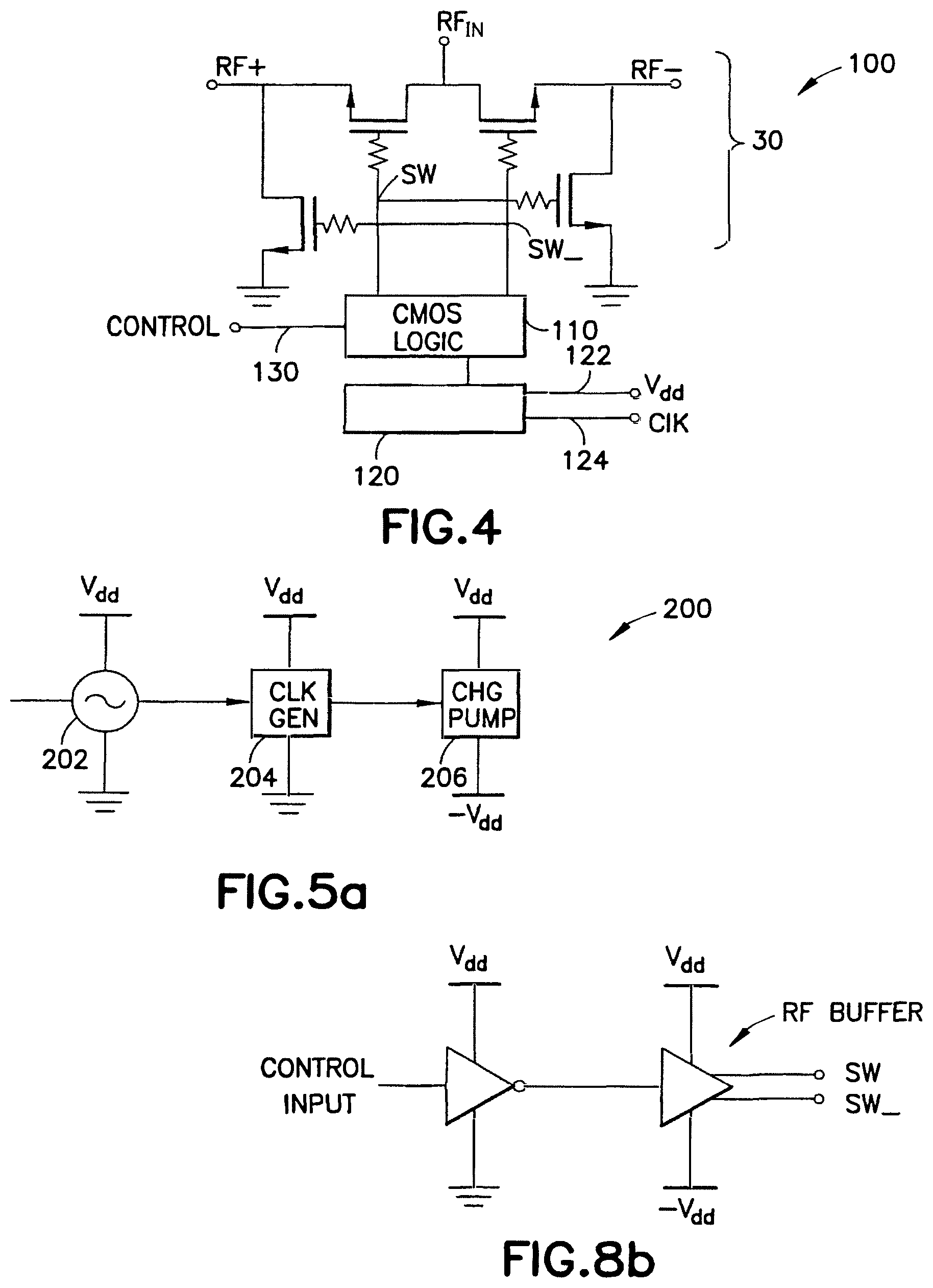
A novel RF switch circuit and method for switching RF signals is described. The RF switch circuit is fabricated in a silicon-on-insulator (SOI) technology. The RF switch includes pairs of switching and shunting transistor groupings used to alternatively couple RF input signals to a common RF node. The switching and shunting transistor grouping pairs are controlled by a switching control voltage (SW) and its inverse (SW_). The switching and shunting transistor groupings comprise one or more MOSFET transistors connected together in a "stacked" or serial configuration. The stacking of transistor grouping devices, and associated gate resistors, increase the breakdown voltage across the series connected switch transistors and operate to improve RF switch compression. A fully integrated RF switch is described including digital control logic and a negative voltage generator integrated together with the RF switch elements. In one embodiment, the fully integrated RF switch includes a built-in oscillator, a charge pump circuit, CMOS logic circuitry, level-shifting and voltage divider circuits, and an RF buffer circuit. Several embodiments of the charge pump, level shifting, voltage divider, and RF buffer circuits are described. The inventive RF switch provides improvements in insertion loss, switch isolation, and switch compression.
| Inventors: | Burgener; Mark L. (San Diego, CA), Cable; James S. (San Diego, CA), Benton; Robert H. (Sunnyvale, CA) | ||||||||||
|---|---|---|---|---|---|---|---|---|---|---|---|
| Applicant: |
|
||||||||||
| Assignee: | pSemi Corporation (San Diego,
CA) |
||||||||||
| Family ID: | 1000005084546 | ||||||||||
| Appl. No.: | 16/679,760 | ||||||||||
| Filed: | November 11, 2019 |
Prior Publication Data
| Document Identifier | Publication Date | |
|---|---|---|
| US 20200076428 A1 | Mar 5, 2020 | |
Related U.S. Patent Documents
| Application Number | Filing Date | Patent Number | Issue Date | ||
|---|---|---|---|---|---|
| 16676350 | Nov 6, 2019 | ||||
| 16167389 | Oct 22, 2018 | ||||
| 15656953 | Dec 11, 2018 | 10153767 | |||
| 14883499 | Oct 3, 2017 | 9780778 | |||
| 14062791 | Dec 29, 2015 | 9225378 | |||
| 12980161 | Nov 12, 2013 | 8583111 | |||
| 12315395 | Dec 28, 2010 | 7860499 | |||
| 11582206 | Dec 2, 2008 | 7460852 | |||
| 10922135 | Oct 17, 2006 | 7123898 | |||
| 10267531 | Oct 12, 2004 | 6804502 | |||
| 60328353 | Oct 10, 2001 | ||||
| Current U.S. Class: | 1/1 |
| Current CPC Class: | H03K 19/0944 (20130101); H03K 19/018521 (20130101); H03K 17/102 (20130101); H03K 17/6871 (20130101); H03K 17/063 (20130101); H04B 1/40 (20130101); H03K 17/693 (20130101); H01P 1/15 (20130101); H03K 2017/0803 (20130101) |
| Current International Class: | H03K 17/687 (20060101); H03K 17/10 (20060101); H03K 17/693 (20060101); H03K 19/0944 (20060101); H04B 1/40 (20150101); H03K 17/08 (20060101); H03K 17/06 (20060101); H01P 1/15 (20060101); H03K 19/0185 (20060101) |
References Cited [Referenced By]
U.S. Patent Documents
| 5095348 | March 1992 | Houston |
| 5350957 | September 1994 | Cooper |
| 5587604 | December 1996 | Machesney et al. |
| 5767721 | June 1998 | Crampton |
| 5784311 | July 1998 | Assaderaghi |
| 5818099 | October 1998 | Burghartz |
| 5821769 | October 1998 | Douseki |
| 5825227 | October 1998 | Kohama |
| 5878331 | March 1999 | Yamamoto |
| 5892400 | April 1999 | Van Saders |
| 6081443 | June 2000 | Morishita |
| 6084255 | July 2000 | Ueda |
| 6094088 | July 2000 | Yano |
| 6100564 | August 2000 | Bryant |
| 6111778 | August 2000 | MacDonald |
| 6201761 | March 2001 | Wollesen |
| 6281737 | August 2001 | Kuang |
| 6341087 | January 2002 | Kunikiyo |
| 6356536 | March 2002 | Repke |
| 6486511 | November 2002 | Nathanson |
| 6498370 | December 2002 | Kim |
| 6519191 | February 2003 | Morishita |
| 6521959 | February 2003 | Kim |
| 6563366 | May 2003 | Kohama |
| 6646305 | November 2003 | Assaderaghi |
| 6804502 | October 2004 | Burgener |
| 7123898 | October 2006 | Burgener |
| 7405982 | July 2008 | Flaker |
| 7460852 | December 2008 | Burgener |
| 7860499 | December 2010 | Burgener |
| 8583111 | November 2013 | Burgener |
| 9225378 | December 2015 | Burgener |
| 9780778 | October 2017 | Burgener |
| 10153767 | December 2018 | Burgener |
| 10680600 | June 2020 | Brindle |
| 2001/0045602 | November 2001 | Maeda |
| 2018/0145678 | May 2018 | Maxim |
| 2019/0238126 | August 2019 | Brindle |
| 2020/0036377 | January 2020 | Brindle |
| 2020/0036378 | January 2020 | Brindle |
| 2020/0067504 | February 2020 | Brindle |
| 2020/0076427 | March 2020 | Burgener |
| 2020/0076428 | March 2020 | Burgener |
| 2020/0112305 | April 2020 | Brindle |
| 2020/0153430 | May 2020 | Burgener |
| 1256521 | Jun 2000 | CN | |||
| 200680025128.7 | Nov 2012 | CN | |||
| 19832565 | Aug 1999 | DE | |||
| 112011103554 | Sep 2013 | DE | |||
| 385641 | Sep 1990 | EP | |||
| 622901 | Nov 1994 | EP | |||
| 782267 | Jul 1997 | EP | |||
| 788185 | Aug 1997 | EP | |||
| 851561 | Jan 1998 | EP | |||
| 913939 | May 1999 | EP | |||
| 625831 | Nov 1999 | EP | |||
| 1006584 | Jun 2000 | EP | |||
| 1451890 | Feb 2001 | EP | |||
| 2387094 | Nov 2001 | EP | |||
| 1925030 | May 2008 | EP | |||
| 2348532 | Jul 2011 | EP | |||
| 2348533 | Jul 2011 | EP | |||
| 2348534 | Jul 2011 | EP | |||
| 2348535 | Jul 2011 | EP | |||
| 2348536 | Jul 2011 | EP | |||
| 1774620 | Oct 2014 | EP | |||
| 2884586 | Jun 2015 | EP | |||
| 3113280 | Jan 2017 | EP | |||
| 1902474 | Apr 2017 | EP | |||
| 5575348 | Jun 1980 | JP | |||
| H01254014 | Oct 1989 | JP | |||
| 2161769 | Jun 1990 | JP | |||
| H0434980 | Feb 1992 | JP | |||
| H04183008 | Jun 1992 | JP | |||
| H05299995 | Nov 1993 | JP | |||
| H06112795 | Apr 1994 | JP | |||
| H06314985 | Nov 1994 | JP | |||
| H06334506 | Dec 1994 | JP | |||
| H07046109 | Feb 1995 | JP | |||
| H07070245 | Mar 1995 | JP | |||
| H07106937 | Apr 1995 | JP | |||
| H08023270 | Jan 1996 | JP | |||
| H08070245 | Mar 1996 | JP | |||
| H08148949 | Jun 1996 | JP | |||
| H08251012 | Sep 1996 | JP | |||
| H08307305 | Nov 1996 | JP | |||
| H08330930 | Dec 1996 | JP | |||
| H098627 | Jan 1997 | JP | |||
| H9041275 | Feb 1997 | JP | |||
| H9055682 | Feb 1997 | JP | |||
| H0992785 | Apr 1997 | JP | |||
| H09148587 | Jun 1997 | JP | |||
| H09163721 | Jun 1997 | JP | |||
| H09181641 | Jul 1997 | JP | |||
| H09186501 | Jul 1997 | JP | |||
| H09200021 | Jul 1997 | JP | |||
| H09200074 | Jul 1997 | JP | |||
| H09238059 | Sep 1997 | JP | |||
| H09243738 | Sep 1997 | JP | |||
| H098621 | Oct 1997 | JP | |||
| H09270659 | Oct 1997 | JP | |||
| H09284114 | Oct 1997 | JP | |||
| H09284170 | Oct 1997 | JP | |||
| H09298493 | Oct 1997 | JP | |||
| H09326642 | Dec 1997 | JP | |||
| H1079467 | Mar 1998 | JP | |||
| H1093471 | Apr 1998 | JP | |||
| 10242826 | Sep 1998 | JP | |||
| 10242829 | Sep 1998 | JP | |||
| H10242477 | Sep 1998 | JP | |||
| H10284736 | Oct 1998 | JP | |||
| H10335901 | Dec 1998 | JP | |||
| H1126776 | Jan 1999 | JP | |||
| H11112316 | Apr 1999 | JP | |||
| H11136111 | May 1999 | JP | |||
| H11163642 | Jun 1999 | JP | |||
| H11163704 | Jun 1999 | JP | |||
| H11205188 | Jul 1999 | JP | |||
| H11274804 | Oct 1999 | JP | |||
| 2000031167 | Jan 2000 | JP | |||
| 2000058842 | Feb 2000 | JP | |||
| 2000101093 | Apr 2000 | JP | |||
| 1998034427 | Jun 2000 | JP | |||
| 2000183353 | Jun 2000 | JP | |||
| 2000188501 | Jul 2000 | JP | |||
| 2000208614 | Jul 2000 | JP | |||
| 2000223713 | Aug 2000 | JP | |||
| 2000243973 | Sep 2000 | JP | |||
| 200029476 | Oct 2000 | JP | |||
| 2000277703 | Oct 2000 | JP | |||
| 2000311986 | Nov 2000 | JP | |||
| 2001007332 | Jan 2001 | JP | |||
| 2003060451 | Feb 2001 | JP | |||
| 2001094114 | Apr 2001 | JP | |||
| 2001119281 | Apr 2001 | JP | |||
| 2001157487 | May 2001 | JP | |||
| 2001156182 | Jun 2001 | JP | |||
| 2001274265 | Oct 2001 | JP | |||
| 2002156602 | May 2002 | JP | |||
| 2000358775 | Jun 2002 | JP | |||
| 2002164441 | Jun 2002 | JP | |||
| 2002290104 | Oct 2002 | JP | |||
| 2003101407 | Apr 2003 | JP | |||
| 2003143004 | May 2003 | JP | |||
| 2003167615 | Jun 2003 | JP | |||
| 2003189248 | Jul 2003 | JP | |||
| 2003332583 | Nov 2003 | JP | |||
| 2003347553 | Dec 2003 | JP | |||
| 2004147175 | May 2004 | JP | |||
| 2004515937 | May 2004 | JP | |||
| 2004166470 | Jun 2004 | JP | |||
| 2004199950 | Jul 2004 | JP | |||
| 2004288978 | Oct 2004 | JP | |||
| 2005515657 | May 2005 | JP | |||
| 2005203643 | Jul 2005 | JP | |||
| 2005251931 | Sep 2005 | JP | |||
| 200551567 | Sep 2006 | JP | |||
| 2009500868 | Jan 2009 | JP | |||
| 2010506156 | Feb 2010 | JP | |||
| 4659826 | Mar 2011 | JP | |||
| 4892092 | Mar 2012 | JP | |||
| 5215850 | Mar 2013 | JP | |||
| 5591356 | Sep 2014 | JP | |||
| 55678106 | Feb 2015 | JP | |||
| 6006219 | Oct 2016 | JP | |||
| WO2015015720 | Mar 2017 | JP | |||
| 2014239233 | Dec 2017 | JP | |||
| 19940027615 | Dec 1994 | KR | |||
| WO86/01037 | Feb 1986 | WO | |||
| WO9523460 | Aug 1995 | WO | |||
| WO9806174 | Feb 1998 | WO | |||
| WO9935695 | Jul 1999 | WO | |||
| WO0227920 | Apr 2002 | WO | |||
| WO03032431 | Apr 2003 | WO | |||
| WO2006038190 | Apr 2006 | WO | |||
| WO07008934 | Jan 2007 | WO | |||
| WO07033045 | Mar 2007 | WO | |||
| WO07035610 | Mar 2007 | WO | |||
| WO09108391 | Sep 2009 | WO | |||
| WO12054642 | Apr 2012 | WO | |||
Other References
|
RF Micro Devices Inc., Invalidity Contentions for U.S. Pat. No. 8,405,147, Dec. 10, 2013 (Civil Case #: 3:12-cv-00911-H-JLB), 324 pages, Doc 8000. cited by applicant . RF Micro Devices Inc., Invalidity Contentions for U.S. Pat. No. 7,910,993, Dec. 10, 2013 (Civil Case #: 3:12-cv-00911-H-JLB), 1697 pages, Doc 8001. cited by applicant . RF Micro Devices Inc., Exhibit listing prior art identified in connection with Invalidity Contentions for U.S. Pat. No. 7,910,993 and U.S. Pat. No. 8,405,147, Dec. 10, 2013, (Civil Case #: 3:12-cv-00911-H-JLB), 21 pages, Doc 8004. cited by applicant . RF Micro Devices Inc., Amended Invalidity Contentions for U.S. Pat. No. 8,405,147, Dec. 10, 2013 (Civil Case #: 3:12-cv-00911-H-JLB), 362 pages, Doc 8006. cited by applicant . RF Micro Devices Inc., Amended Invalidity Contentions for U.S. Pat. No. 7,910,993, Dec. 10, 2013 (Civil Case #: 3:12-cv-00911-H-JLB), 110 pages, Doc 8007. cited by applicant . RF Micro Devices Inc., Amended Exhibit listing prior art identified in connection with Invalidity Contentions for U.S. Pat. No. 7,910,993 and U.S. Pat. No. 8,405,147, Dec. 10, 2013, (Civil Case #: 3:12-cv-00911-H-JLB), 33 pages, Doc 8005. cited by applicant . RF Micro Devices Inc., Invalidity Contentions for U.S. Pat. No. 7,860,499, Dec. 10, 2013 (Civil Case #: 3:12-cv-00911-H-JLB), 403 pages, Doc 8002. cited by applicant . RF Micro Devices Inc., Invalidity Contentions for U.S. Pat. No. 7,123,898, Dec. 10, 2013 (Civil Case #: 3:12-cv-00911-H-JLB), 383 pages, Doc 8003. cited by applicant . RF Micro Devices Inc., Amended Invalidity Contentions for U.S. Pat. No. 7,860,499, Dec. 10, 2013 (Civil Case #: 3:12-cv-00911-H-JLB), 445 pages, Doc 8008. cited by applicant . RF Micro Devices Inc., Amended Invalidity Contentions for U.S. Pat. No. 7,123,898, Dec. 10, 2013 (Civil Case #: 3:12-cv-00911-H-JLB), 430 pages, Doc 8009. cited by applicant . RF Micro Devices Inc., Invalidity Contentions for U.S. Pat. No. 7,860,499, Dec. 10, 2013 (Civil Case #: 3:12-cv-00911-H-JLB), 403 pages, Doc 8010. cited by applicant . RF Micro Devices Inc., Invalidity Contentions for U.S. Pat. No. 7,123,898, Dec. 10, 2013 (Civil Case #: 3:12-cv-00911-H-JLB), 383 pages, Doc 8011. cited by applicant . RF Micro Devices Inc., Amended Invalidity Contentions for U.S. Pat. No. 7,860,499, Dec. 10, 2013 (Civil Case #: 3:12-cv-00911-H-JLB), 445 pages, Doc 8012. cited by applicant . RF Micro Devices Inc., Amended Invalidity Contentions for U.S. Pat. No. 7,123,898, Dec. 10, 2013 (Civil Case #: 3:12-cv-00911-H-JLB), 504 pages, Doc 8013. cited by applicant . Docket for Case No. CACD-8-12-cv-00248 filed Feb. 14, 2012 in the United States District Court, Central District of California, Southern Division, 4 pages, Doc 8022. cited by applicant . Docket for Case 377-TA-848 filed Feb. 14, 2012 in the International Trade Commission, 14 pages, Doc 8023. cited by applicant . Docket for Case No. CASD-3-12-cv-00911 filed Feb. 13, 2012 in the United States District Court, Central District of California, Southern Division, 42 pages, Doc 8024. cited by applicant . Docket for Case No. CASD-3-12-cv-01160 filed May 11, 2012 in the United States District Court, Central District of California, Southern Division, 10 pages, Doc 8025. cited by applicant . Docket for Case No. CASD-3-13-cv-00725 filed Mar. 26, 2013 in the United States District Court, Central District of California, Southern Division, 4 pages, Doc 8026. cited by applicant . Docket for Case No. NCMD-1-12-cv-00377 filed Apr. 16, 2012 in the United States District Court, North Carolina Middle District, 5 pages, Doc 8027. cited by applicant . Peregrine's Verified Complaint filed with ITC Feb. 14, 2012 in 337-TA-848, 39 pages, Doc 8067. cited by applicant . Peregrine's Letter to Supplement Feb. 14, 2012 Complaint filed Feb. 16, 2012 in 337-TA-848, 1 page, Doc 8080. cited by applicant . Peregrine's Letter to Clarify and Supplement Feb. 14, 2012 Complaint filed Feb. 28, 2012 in 337-TA-848, 1 page, Doc 8081. cited by applicant . Peregrine's First Amended Complaint filed May 11, 2012 in 337-TA-848, 38 pages, Doc 8068. cited by applicant . Peregrine's Errata to Correct Typographical Error in Peregrine's First Amended Complaint filed May 15, 2012 in 337-TA-848, 2 pages, Doc 8071. cited by applicant . HTC's Response to First Amended Complaint filed Jul. 2, 2012 in 337-TA-848, 22 pages, Doc 8070. cited by applicant . Motorola's Exhibit A to the Response to Amended Complaint filed Jul. 2, 2012 in 337-TA-848, 3 pages, Doc 8073. cited by applicant . Motorola's Response to Amended Complaint filed Jul. 2, 2012 in 337-TA-848, 24 pages, Doc 8074. cited by applicant . RFMD's Response to First Amended Complaint filed Jul. 2, 2012 in 337-TA-848, 26 pages, Doc 8078. cited by applicant . HTC's Response to Amended Complaint filed Jul. 3, 2012 in 337-TA-848, 3 pages, Doc 8069. cited by applicant . Peregrine's Appendices A and I to Accompany First Amended Complaint filed Jul. 3, 2012 in 337-TA-848, 2 pages, Doc 8076. cited by applicant . Peregrine's Motion for Leave to Amend Complaint filed Jul. 20, 2012 in 337-TA-848, 87 pages, Doc 8077. cited by applicant . Peregrine's Letter to Supplement First Amended Complaint filed Jul. 25, 2012 in 337-TA-848, 3 pages, Doc 8072. cited by applicant . Peregrine's Notice of Patent Priority Dates filed Aug. 22, 2012 in 337-TA-848, 4 pages, Doc 8075. cited by applicant . Commission Investigative Staff's Notice of Prior Art filed Aug. 31, 2012 in 337-TA-848, 3 pages, Doc 8079. cited by applicant . Peregrine's Complaint for Damages and Injunctive Relief filed Feb. 14, 2012 in CACD-8-12-cv-00248, 101 pages, Doc 8082. cited by applicant . Peregrine's Complaint for Injunctive Relief filed Apr. 13, 2012 in CASD-3-12-cv-00911, 199 pages, Doc 8030. cited by applicant . RFMD and Motorola's Answer to Complaint and RFMD's Counterclaim filed Jun. 8, 2012 in CASD-3-12-cv-00911, 18 pages, Doc 8031. cited by applicant . RFMD's Answer, Defenses and Counterclaims to Plaintiff's Complaint filed May 1, 2013 in CASD-3-12-cv-00911, 11 pages, Doc 8032. cited by applicant . Peregrine's Answer to RFMD's Counterclaims filed May 28, 2013 in CASD-3-12-cv-00911, 10 pages, Doc 8033. cited by applicant . Peregrine's First Amended Complaint filed Nov. 21, 22013 in CASD-3-12-cv-00911, 348 pages, Doc 8035. cited by applicant . Peregrine's Motion for Preliminary Injunction filed Nov. 25, 2013 in CASD-3-12-cv-00911, 327 pages., Doc 8036. cited by applicant . RFMD's Amended Answer, Defenses and Counterclaims to Plaintiff's Complaint (Redacted Public Version) filed Dec. 12, 2013 in CASD-3-12-cv-00911, 65 pages, Doc 8034. cited by applicant . Defendant RFMD's Opposition to Peregrine's Motion for Preliminary Injunction filed Dec. 13, 2013 in CASD-3-12-cv-00911, 504 pages, Docs 8028A-8028D. cited by applicant . Peregrine's Reply in Support of Its Motion for Preliminary Injunction (Public Redacted Version) filed Dec. 20, 2013 in CASD-3-12-cv-00911, 130 pages, Doc 8037. cited by applicant . RFMD's Unopposed Motion for Leave to File Short Surreply in Opposition to Peregrine's Motion for Preliminary Injunction filed Jan. 3, 2014 in CASD-3-12-cv-00911, 60 pages, Doc 8038. cited by applicant . Peregrine's Unopposed Motion for Leave to File Response to RFMD's Surreply filed Jan. 3, 2014 in CASD-3-12-cv-00911, 15 pages, Doc 8039. cited by applicant . Peregrine's Answer and Counterclaims to RFMD's Counterclaims filed Jan. 6, 2014 in CASD-3-12-cv-00911, 23 pages, Doc 8040. cited by applicant . Order Denying Peregrine's Motion for Preliminary Injunction filed Jan. 8, 2014 in CASD-3-12-cv-00911, 7 pages, Doc 8041. cited by applicant . RFMD's Answer to Peregrine's Counterclaims filed Jan. 27, 2014 in CASD-3-12-cv-00911, 5 pages, Doc 8042. cited by applicant . RFMD's Motion to Dismiss Peregrine's 3rd, 4th, 6th, 7th and 8th Counts for Lack of Subject Matter Jurisdiction filed Jan. 30, 2014 in CASD-3-12-cv-00911, 323 pages, Doc 8043. cited by applicant . Defendant Benton's Answer and Defenses to Plaintiff's First Amended Complaint filed Jan. 31, 2014 in CASD-3-12-cv-00911, 36 pages, Doc 8044. cited by applicant . Joint Claim Construction and Prehearing Statement Pursuant to Patent L.R. 4.2 filed Feb. 4, 2014 in CASD-3-12-cv-00911, 176 pages, Doc 8045. cited by applicant . Defendant Benton's Notice of Joinder to RFMD's Motion to Dismiss and Motion and Memorandum in Support of Motion to Dismiss Peregrine's 1st, 2nd, and 3rd Causes of Action for Lack of Subject Matter Jurisdiction filed Feb. 26, 2014 in CASD-3-12-cv-00911, 13 pages, Doc 8046. cited by applicant . Peregrine's Memorandum in Opposition to RFMD's Motion to Dismiss filed Mar. 3, 2014 in CASD-3-12-cv-00911, 184 pages, Doc 8047. cited by applicant . Peregrine's Opening Claim Construction Brief filed Mar. 4, 2014 in CASD-3-12-cv-00911, 377 pages, Docs 8029A and 8029B. cited by applicant . RFMD's Opening Brief on Claim Construction (Public Redacted Version) filed Mar. 4, 2014 in CASD-3-12-cv-00911, 27 pages, Doc 8048. cited by applicant . RFMD's Declaration of Mark Tung in Support of RFMD's Opening Claim Construction Brief filed Mar. 4, 2014 in CASD-3-12-cv-00911, 162 pages, Doc 8049. cited by applicant . RFMD's Reply Memorandum in Support of Its Motion to Dismiss Peregrine's 4th, 6th, 7th and 8th Counts for Lack of Subject Matter Jurisdiction filed Mar. 10, 2014 in CASD-3-12-cv-00911, 37 pages, Doc 8051. cited by applicant . Peregrine's Memorandum in Opposition to Benton's Motion to Dismiss (Public Redacted Version) filed Mar. 14, 2014 in CASD-3-12-cv-00911, 86 pages, Doc 8052. cited by applicant . Order (1) Granting in Part and Denying in Part RFMD's Motion to Dismiss; (2) Granting Benton's Motion to Dismiss; and (3) Denying Peregrine's Motion to Stay filed Mar. 18, 2014 in CASD-3-12-cv-00911, 10 pages, Doc 8053. cited by applicant . Stricken Document: Response to Claim Construction Brief Pursuant to Order 214 filed Mar. 18, 2014 in CASD-3-12-cv-00911, 1 page, Doc 8054. cited by applicant . Declaration of Brian Floyd, Ph.D. filed Mar. 4, 2016 in CASD-3-12-cv-00911, 23 pages, Doc 8050. cited by applicant . Peregrine's Complaint for Damages and Injunctive Relief filed May 11, 2012 in CASD-3-12-cv-01160, 9 pages, Doc 8083. cited by applicant . RFMD's Complaint for Declaratory Judgment of Patent Non-Infringement and Invalidity filed Apr. 16, 2012 in NCMD-1-12-cv-00377, 246 pages, Doc 8085. cited by applicant . Brinkman--Respondents' Notice of Prior Art, Investigation No. 337-TA-848, dated Aug. 31, 2012, 59 pages, Doc 0825. cited by applicant . Burgener--U.S. Appl. No. 10/267,531, filed Oct. 8, 2002, 72 pages, Doc 4339. cited by applicant . USPTO--Notice to File Corrected Application Papers dated Nov. 12, 2002 for U.S. Appl. No. 10/267,531, 1 page, Doc 4340. cited by applicant . Burgener--Response to Notice to File Corrected Application Papers and Replacement Figures dated Jan. 13, 2003 for U.S. Appl. No. 10/267,531, 16 pages, Doc 4341. cited by applicant . Burgener--Power 33of Attorney for Peregrine Semiconductor dated Feb. 4, 2003 for U.S. Appl. No. 10/267,531, 3 pages, Doc 4342. cited by applicant . USPTO--Acceptance of Power of Attorney dated Jan. 2, 2004 for U.S. Appl. No. 10/267,531, 1 page, Doc 4343. cited by applicant . USPTO--Notice of Allowance dated May 12, 2004 for U.S. Appl. No. 10/267,531, 32 pages, Doc 4344. cited by applicant . Burgener--Issue Fee Payment and Comments on Reasons for Allowance dated Aug. 12, 2004 for U.S. Appl. No. 10/267,531, 3 pages, Doc 4345. cited by applicant . Burgener--Request for Certificate of Correction dated Feb. 10, 2005 for U.S. Appl. No. 10/267,531, 2 pages, Doc 4346. cited by applicant . USPTO--Certificate of Correction dated Apr. 26, 2005 for U.S. Appl. No. 10/267,531, 1 page, Doc 4347. cited by applicant . Burgener--Request for Certificate of Correction dated Dec. 13, 2006 for U.S. Appl. No. 10/267,531, 1 page, Doc 4348. cited by applicant . USPTO--Certificate of Correction dated May 1, 2007 for U.S. Appl. No. 10/267,531, pages, Doc 4349. cited by applicant . Burgener--U.S. Appl. No. 10/922,135, filed Aug. 18, 2004, 63 pages, Doc 4350. cited by applicant . USPTO--Office Action dated Jun. 3, 2005 for U.S. Appl. No. 10/922,135, 11 pages, Doc 4351. cited by applicant . Burgener--Amendment dated Dec. 7, 2005 for U.S. Appl. No. 10/922,135, 10 pages, Doc 4352. cited by applicant . USPTO--Final Office Action dated Jan. 17, 2006 for U.S. Appl. No. 10/922,135, 9 pages, Doc 4353. cited by applicant . Burgener--Amendment dated May 19, 2006 for U.S. Appl. No. 10/922,135, 6 pages, Doc 4354. cited by applicant . USPTO--Notice of Allowance dated Jun. 2, 2006 for U.S. Appl. No. 10/922,135, 11 pages, Doc 4355. cited by applicant . Burgener--Issue Fee Payment dated Sep. 8, 2006 for U.S. Appl. No. 10/922,135, 1 page, Doc 4356. cited by applicant . Burgener--Request for Certificate of Correction dated Jul. 1, 2008 for U.S. Appl. No. 10/922,135, 3 pages, Doc 4358. cited by applicant . USPTO--Certificate of Correction dated Aug. 12, 2008 for U.S. Appl. No. 10/922,135, 1 page, Doc 4359. cited by applicant . Burgener--Amendment after final dated Apr. 25, 2009 for U.S. Appl. No. 10/922,135, 7 pages, Doc 4357. cited by applicant . USPTO--Report on the Determination of an Action Regarding a Patent or Trademark 3:12-cv-1160-CAB-BGS dated Jun. 11, 2012 for U.S. Appl. No. 10/922,135, 1 page, Doc 4360. cited by applicant . USPTO--Report on the Determination of an Action Regarding a Patent or Trademark 1:12CV377 dated Jul. 11, 2012 for U.S. Appl. No. 10/922,135, 13 pages, Doc 4361. cited by applicant . USPTO--Report on the Determination of an Action Regarding a Patent or Trademark 3:12-CV-1160-CAB-BGS) dated Apr. 15, 2013 for U.S. Appl. No. 10/922,135, 1 page, Doc 4363. cited by applicant . USPTO--Report on the 333Determination of an Action Regarding a Patent or Trademark SACV12-248 JST(RNBx) dated Dec. 21, 2013 for U.S. Appl. No. 10/922,135, 1 page, Doc 4362. cited by applicant . Burgener--Change of Address and Notification of Loss of Small Entity Status dated Mar. 5, 2014 for U.S. Appl. No. 10/922,135, 5 pages, Doc 4364. cited by applicant . USPTO--Report on the Determination of an Action Regarding a Patent or Trademark 3:12-CV-0911-AJB-WMC) dated Oct. 14, 2014 for U.S. Appl. No. 10/922,135, 1 page, Doc 4365. cited by applicant . Burgener--Notification of Loss of Small Entity Status dated Jun. 5, 2017 for U.S. Appl. No. 10/922,135, 1 page, Doc 4366. cited by applicant . Burgener--U.S. Appl. No. 11/582,206, filed Oct. 16, 2006, 65 pages, Doc 4385. cited by applicant . USPTO--Filing Receipt dated Nov. 3, 2006 for U.S. Appl. No. 11/582,206, 3 pages, Doc 4386. cited by applicant . USPTO--Notice of Publication dated May 31, 2007 for U.S. Appl. No. 11/582,206, 1 page, Doc 4387. cited by applicant . USPTO--Office Action dated Nov. 15, 2007 for U.S. Appl. No. 11/582,206, 12 pages, Doc 4388. cited by applicant . Burgener--Amendment and Terminal Disclaimers dated May 19, 2008 for U.S. Appl. No. 11/582,206, 15 pages, Doc 4389. cited by applicant . Tieu--Notice of Allowance dated Jul. 15, 2008 for U.S. Appl. No. 11/582,206, 12 pages, Doc 0668. cited by applicant . USPTO--Notice of Allowance dated Jul. 15, 2008 for U.S. Appl. No. 11/582,206, 12 pages, Doc 4390. cited by applicant . Burgener--Issue Fee Payment dated Oct. 20, 2008 for U.S. Appl. No. 11/582,206, 2 pages, Doc 4391. cited by applicant . USPTO--Supplemental Non-Final Rejection dated Oct. 30, 2008 for U.S. Appl. No. 11/582,206, 4 pages, Doc 4392. cited by applicant . USPTO--Issue Notification dated Nov. 12, 2008 for U.S. Appl. No. 11/582,206, 1 page, Doc 4393. cited by applicant . USPTO--Report on the Filing or Determination of an Action Regarding a Patent 3:12-cv-001160-CAB-BGS dated Jun. 11, 2012 for U.S. Appl. No. 11/582,206, 1 page, Doc 4394. cited by applicant . USPTO--Report on the Filing or Determination of an Action Regarding a Patent 8:12-cv-00248-JST-RNB dated Feb. 21, 2013 for U.S. Appl. No. 11/582,206, 1 page, Doc 4396. cited by applicant . USPTO--Report on the Filing or Determination of an Action Regarding a Patent 8:12-cv-1160-CAB-BGS dated Apr. 15, 2013 for U.S. Appl. No. 11/582,206, 1 page, Doc 4397. cited by applicant . USPTO--Report on the Filing or Determination of an Action Regarding a Patent 8:12-cv-00911-AJB-WMC dated Oct. 14, 2014 for U.S. Appl. No. 11/582,206, 1 page, Doc 4398. cited by applicant . Burgener--Notification of Loss of Small Entity Status dated Sep. 9, 2015 for U.S. Appl. No. 11/582,206, 1 page, Doc 4399. cited by applicant . Burgener--U.S. Appl. No. 12/315,395, filed Dec. 1, 2008, 65 pages, Doc 4400. cited by applicant . USPTO--Notice of Publication dated May 7, 2009 for U.S. Appl. No. 12/315,395, 1 page, Doc 4402. cited by applicant . USPTO--Notice of Allowance dated Aug. 11, 2010 for U.S. Appl. No. 12/315,395, 33 pages, Doc 4403. cited by applicant . USPTO--Supplemental Notice of Allowability dated Oct. 29, 2010 for U.S. Appl. No. 12/315,395, 10 pages, Doc 4404. cited by applicant . Burgener--Issue Fee Payment dated Nov. 16, 2010 for U.S. Appl. No. 12/315,395, 1 page, Doc 4405. cited by applicant . USPTO--Issue Notification dated Dec. 8, 2010 for U.S. Appl. No. 12/315,395, 1 page, Doc 4406. cited by applicant . USPTO--Report on the Filing or Determination of an Action Regarding a Patent 3:12-cv-001160-CAB-BGS dated Jun. 11, 2012 for U.S. Appl. No. 12/315,395, 1 page, Doc 4407. cited by applicant . USPTO--Report on the Filing or Determination of an Action Regarding a Patent 1:12cv377 dated Jul. 11, 2012 for U.S. Appl. No. 12/315,395, 13 pages, Doc 4408. cited by applicant . USPTO--Report on the Filing or Determination of an Action Regarding a Patent 8:12-cv-1160-CAB-BGS dated Apr. 15, 2013 for U.S. Appl. No. 12/315,395, 1 page, Doc 4409. cited by applicant . Burgener--Change of Address and Notification of Loss of Small Entity Status dated Mar. 7, 2014 for U.S. Appl. No. 12/315,395, 5 pages, Doc 4410. cited by applicant . USPTO--Report on the Filing or Determination of an Action Regarding a Patent dated Oct. 14, 2014 for U.S. Appl. No. 12/315,395, 1 page, Doc 4411. cited by applicant . Burgener--Request for Certificate of Correction dated Mar. 7, 2016 for U.S. Appl. No. 12/315,395, 5 pages, Doc 4412. cited by applicant . USPTO--Certificate of Correction dated May 10, 2016 for U.S. Appl. No. 12/315,395, 1 page, Doc 4413. cited by applicant . Burgener--Notification of Loss of Small Entity Status dated Jun. 5, 2017 for U.S. Appl. No. 12/315,395, 1 page, Doc 4414. cited by applicant . USPTO--Filing Receipt dated Jan. 27, 2019 for U.S. Appl. No. 12/315,395, 3 pages, Doc 4401. cited by applicant . Burgener--U.S. Appl. No. 12/980,161, filed Dec. 28, 2010, 68 pages, Doc 4415. cited by applicant . USPTO--Filing Receipt dated Jan. 13, 2011 for U.S. Appl. No. 12/980,161, 4 pages, Doc 44160. cited by applicant . USPTO--Notice of Publication dated Apr. 21, 2011 for U.S. Appl. No. 12/980,161, 1 page, Doc 4417. cited by applicant . Burgener--Preliminary Amendment dated Apr. 27, 2012 for U.S. Appl. No. 12/980,161, 28 pages, Doc 4418. cited by applicant . USPTO--Notice of Non-Compliant Amendment dated May 1, 2012 for U.S. Appl. No. 12/980,161, 2 pages, Doc 4419. cited by applicant . Burgener--Response to Notice of Non-Compliant Amendment--Preliminary.Amendment dated May 17, 2012 for U.S. Appl. No. 12/980,161, 6 pages, Doc 4420. cited by applicant . USPTO--Office Action dated Feb. 19, 2013 for U.S. Appl. No. 12/980,161, 106 pages, Doc 4421. cited by applicant . Burgener--Amendment and Terminal Disclaimers dated Aug. 19, 2013 for U.S. Appl. No. 12/980,161, 32 pages, Doc 4422. cited by applicant . USPTO--Terminal Disclaimer Decision dated Aug. 21, 2013 for U.S. Appl. No. 12/980,161, 1 page, Doc 4423. cited by applicant . USPTO--Notice of Allowance dated Sep. 30, 2013 for U.S. Appl. No. 12/980,161, 186 pages, Doc 4424. cited by applicant . Burgener--Issue Fee Payment dated Oct. 8, 2013 for U.S. Appl. No. 12/980,161, 6 pages, Doc 4425. cited by applicant . USPTO--Issue Notification dated Oct. 23, 2013 for U.S. Appl. No. 12/980,161, 1 page, Doc 4426. cited by applicant . Burgener--Change of Address dated Nov. 8, 2013 for U.S. Appl. No. 12/980,161, 4 pages, Doc 4427. cited by applicant . Burgener--Request for Certificate of Correction dated Aug. 29, 2014 for U.S. Appl. No. 12/980,161, 7 pages, Doc 4428. cited by applicant . USPTO--Certificate of Correction dated Oct. 21, 2014 for U.S. Appl. No. 12/980,161, 1 page, Doc 4429. cited by applicant . Burgener--Notice of Loss of Small Entity Status dated Aug. 18, 2016 for U.S. Appl. No. 12/980,161, 1 page, Doc 4430. cited by applicant . Burgener--U.S. Appl. No. 14/062,791, filed Oct. 24, 2013, 66 pages, Doc 4431. cited by applicant . USPTO--Filing Receipt and Notice to File Missing Parts dated Nov. 12, 2013 for U.S. Appl. No. 14/062,791, 6 pages, Doc 4432. cited by applicant . Burgener--Response to Pre-Exam Formalities Notice dated Jan. 13, 2014 for U.S. Appl. No. 14/062,791, 15 pages, Doc 4470. cited by applicant . USPTO--Updated Filing Receipt and Acceptance of Power of Attorney dated Mar. 20, 2014 for U.S. Appl. No. 14/062,791, 5 pages, Doc 4471. cited by applicant . USPTO--Office Action dated Jun. 24, 2014 for U.S. Appl. No. 14/062,791, 10 pages, Doc 4472. cited by applicant . USPTO--Notice of Publication dated Jun. 30, 2014 for U.S. Appl. No. 14/062,791, 1 page, Doc 4473. cited by applicant . Burgener--Amendment and Terminal Disclaimer filed Nov. 24, 2014 for U.S. Appl. No. 14/062,791, 18 pages, Doc 4474. cited by applicant . USPTO--Terminal Disclaimer Decision dated Dec. 9, 2014 for U.S. Appl. No. 14/062,791, 1 page, Doc 4475. cited by applicant . USPTO--Notice of Allowance dated Jan. 23, 2015 for U.S. Appl. No. 14/062,791, 15 pages, Doc 4476. cited by applicant . USPTO--Notice of Allowance dated May 14, 2015 for U.S. Appl. No. 14/062,791, 11 pages, Doc 4477. cited by applicant . Burgener--Request for Continued Examination filed Aug. 14, 2015 in U.S. Appl. No. 14/062,791, 3 pages, Doc 4478. cited by applicant . USPTO--Notice of Allowance dated Sep. 4, 2015 for U.S. Appl. No. 14/062,791, 17 pages, Doc 4479. cited by applicant . Burgener--Issue Fee Payment dated Oct. 7, 2015 for U.S. Appl. No. 14/062,791, 5 pages, Doc 4480. cited by applicant . USPTO--Notice of Allowance dated Oct. 16, 2015 for U.S. Appl. No. 14/062,791, 8 pages, Doc 4481. cited by applicant . USPTO--Issue Notification dated Dec. 9, 2015 for U.S. Appl. No. 14/062,791, 1 page, Doc 4482. cited by applicant . Burgener--Application dated Oct. 14, 2015, U.S. Appl. No. 14/883,499, 66 pages, Doc 6025. cited by applicant . USPTO--Filing Receipt dated Nov. 2, 2015, U.S. Appl. No. 14/883,499, 4 pages, Doc 6026. cited by applicant . USPTO--Notice of Missing Parts dated Nov. 2, 2015, U.S. Appl. No. 14/883,499, 2 pages, Doc 6027. cited by applicant . Bergener--Response to Missing Parts dated Jan. 4, 2016, U.S. Appl. No. 14/883,499, 15 pages, Doc 6028. cited by applicant . USPTO--Updated Filing Receipt dated Mar. 24, 2016, U.S. Appl. No. 14/883,499, 6 pages, Doc 6029. cited by applicant . USPTO--Notice of Publication dated Jun. 30, 2016, U.S. Appl. No. 14/883,499, 1 page, Doc 6030. cited by applicant . USPTO--Office Action dated Oct. 4, 2016, U.S. Appl. No. 14/883,499, 26 pages, Doc 6031. cited by applicant . Burgener--Response to Office Action dated Feb. 3, 2017, U.S. Appl. No. 14/883,499, 16 pages, Doc 6032. cited by applicant . USPTO--Final Office Action dated May 18, 2017, U.S. Appl. No. 14/883,499, 24 pages, Doc 6033. cited by applicant . Burgener--Response to Final Office Action & Terminal Disclaimers dated May 26, 2017, U.S. Appl. No. 14/883,499, 19 pages, Doc 6034. cited by applicant . USPTO--Terminal Disclaimer Decision dated May 30, 2017, U.S. Appl. No. 14/883,499, 1 page, Doc 6035. cited by applicant . USPTO--Notice of Allowance dated Jun. 8, 2017, U.S. Appl. No. 14/883,499, 21 pages, Doc 6036. cited by applicant . Burgener--Issue Fee Payment dated Jul. 10, 2017, U.S. Appl. No. 14/883,499, 8 pages, Doc 6037. cited by applicant . Burgener--RCE dated Jul. 13, 2017, U.S. Appl. No. 14/883,499, 3 pages, Doc 6038. cited by applicant . Burgener--Petition to Withdraw from Issuance dated Jul. 13, 2017, U.S. Appl. No. 14/883,499, 2 pages, Doc 6039. cited by applicant . USPTO--Decision on Petition to Withdraw from Issuance dated Jul. 13, 2017, U.S. Appl. No. 14/883,499 1 pages, Doc 6040. cited by applicant . Burgener--Petition to Accept Delayed Priority Claim dated Jul. 17, 2017, U.S. Appl. No. 14/883,499, 13 pages, Doc 6041. cited by applicant . USPTO--Notice of Allowance dated Aug. 3, 2017, U.S. Appl. No. 14/883,499, 42 pages, Doc 6042. cited by applicant . USPTO--Corrected Filing Receipt dated Aug. 17, 2017, U.S. Appl. No. 14/883,499, 4 pages, Doc 6043. cited by applicant . USPTO--Decision on Petition to Accept Delayed Priority Claim dated Aug. 21, 2017, U.S. Appl. No. 14/883,499, 9 pages, Doc 6044. cited by applicant . Burgener--Issue Fee Payment dated Aug. 22, 2017, U.S. Appl. No. 14/883,499, 7 pages, Doc 6045. cited by applicant . Acceptance of Publication Request dated Aug. 23, 2017, U.S. Appl. No. 14/883,499, 1 page, Doc 6046. cited by applicant . USPTO--Supplemental Notice of Allowability dated Aug. 30, 2017, U.S. Appl. No. 14/883,499, 6 pages, Doc 6047. cited by applicant . USPTO--Issue Notification dated Sep. 13, 2017, U.S. Appl. No. 14/883,499, 1 page, Doc 6048. cited by applicant . Burgener--U.S. Appl. No. 15/656,953, filed Jul. 21, 2017, 71 pages, Doc 6005. cited by applicant . USPTO--Filing Receipt dated Aug. 4, 2017, U.S. Appl. No. 15/656,953, 4 pages, Doc 6006. cited by applicant . USPTO--Missing Parts dated Aug. 4, 2017, U.S. Appl. No. 15/656,953, 2 pages, Doc 6007. cited by applicant . Burgener--Response to Notice to File Missing Parts for U.S. Appl. No. 15/656,953, dated Oct. 4, 2017, 13 pages, Doc 6008. cited by applicant . Burgener--Preliminary Amendment dated Nov. 17, 2017, U.S. Appl. No. 15/656,953, 11 pages, Doc 6009. cited by applicant . USPTO--Updated Filing Receipt dated Nov. 22, 2017, U.S. Appl. No. 15/656,953, 4 pages, Doc 6010. cited by applicant . USPTO--Notice of Publication dated Mar. 1, 2018, U.S. Appl. No. 15/656,953, 1 page, Doc 6011. cited by applicant . USPTO--Office Action dated Mar. 7, 2018, U.S. Appl. No. 15/656,953, 21 pages, Doc 6012. cited by applicant . Burgener--Request to Update Applicant Name dated Apr. 8, 2018, U.S. Appl. No. 15/656,953 8 pages, Doc 6013. cited by applicant . USPTO--Corrected Filing Receipt dated Apr. 10, 2018 for U.S. Appl. No. 15/656,953, 4 pages, Doc 6014. cited by applicant . Burgener--Response to Office Action dated Apr. 19, 2018, U.S. Appl. No. 15/656,953, 4 pages, Doc 6015. cited by applicant . USPTO--Terminal Disclaimer dated Apr. 19, 2018 for U.S. Appl. No. 15/656,953, 3 pages, Doc 6016. cited by applicant . USPTO--Final Office Action dated May 16, 2018, U.S. Appl. No. 15/656,953, 17 pages, Doc 6017. cited by applicant . Burgener--Response to Final Office Action dated Jul. 12, 2018, U.S. Appl. No. 15/656,953, 3pages, Doc 6018. cited by applicant . USPTO--Notice of Allowance dated Aug. 1, 2018, U.S. Appl. No. 15/656,953, 20 pages, Doc 6019. cited by applicant . Burgener--Rule 312 Amendment dated Sep. 19, 2018, U.S. Appl. No. 15/656,953, Doc 6020. cited by applicant . USPTO--Response to Rule 312 Amendment dated Sep. 27, 2018, U.S. Appl. No. 15/656,953, 3 pages, Doc 6021. cited by applicant . USPTO--Supplemental Notice of Allowability dated Oct. 12, 2018, U.S. Appl. No. 15/656,953, 14 pages, Doc 6022. cited by applicant . Burgener--Issue Fee Payment dated Oct. 19, 2018, U.S. Appl. No. 15/656,953, 5 pages, Doc 6023. cited by applicant . USPTO--Issue Notification dated Nov. 20, 2018, U.S. Appl. No. 15/656,953, 1 page, Doc 6024. cited by applicant . Burgener--U.S. Appl. No. 16/167,389, filed Oct. 22, 2018, 76 pages, Doc 6000. cited by applicant . USPTO--Filing Receipt dated Nov. 16, 2018, U.S. Appl. No. 16/167,389, 4 pages, Doc 6001. cited by applicant . USPTO--Notice of Publication dated Feb. 21, 2019 for U.S. Appl. No. 16/167,389, 1 page, Doc 6002. cited by applicant . USPTO--Office Action dated Mar. 22, 2019 for U.S. Appl. No. 16/167,389, 20 pages, Doc 6003. cited by applicant . USPTO--Terminal Disclaimer dated Mar. 28, 2019 for U.S. Appl. No. 16/167,389, 7 pages, Doc 6004. cited by applicant . Burgener--Response to Office Action filed Aug. 22, 2019 for U.S. Appl. No. 16/167,389, 24 pages, Doc 9027. cited by applicant . USPTO--Notice of Allowance and Notice of Allowability for U.S. Appl. No. 16/167,389 dated Oct. 10, 2019, 89 pages--Doc 9003. cited by applicant . Burgener--Issue Fee Payment and 312 Amendment filed Jan. 10, 2020 for U.S. Appl. No. 16/167,389, 11 pages, Doc 9070. cited by applicant . USPTO--Response to 312 Amendment dated Jan. 30, 2020 for U.S. Appl. No. 16/167,389, 11 pages, Doc 9082. cited by applicant . USPTO--Issue Notification dated Feb. 12, 2020 for U.S. Appl. No. 16/167,389, 1 page, Doc 9093. cited by applicant . USPTO--Supplemental Notice of Allowability dated Mar. 9, 2020 for U.S. Appl. No. 16/167,389, 8 pages, Doc 9100. cited by applicant . USPTO--Issue Notification dated Mar. 25, 2020 for U.S. Appl. No. 16/167,389, 1 page, Doc 9102. cited by applicant . Burgener--U.S. Appl. No. 16/676,350, filed Nov. 6, 2019, 92 pages, Doc 9004. cited by applicant . USPTO--Non-final Office Action dated Dec. 26, 2019 for U.S. Appl. No. 16/676,350, 17 pages, Doc 9029. cited by applicant . Burgener--U.S. Appl. No. 16/738,343, filed Jan. 9, 2020, 92 pages, Doc 9068. cited by applicant . USPTO--Filing Receipt dated Jan. 31, 2020 for U.S. Appl. No. 16/679,760, 4 pages, Doc 9085. cited by applicant . USPTO--Acceptance of Track I Request dated Feb. 4, 2020 for U.S. Appl. No. 16/679,760, 2 pages, Doc 9095. cited by applicant . USPTO--Non-final Office Action dated Feb. 25, 2020 for U.S. Appl. No. 16/738,343, 24 pages, Doc 9096. cited by applicant . Kelly--U.S. Appl. No. 11/347,014, filed Feb. 3, 2006, 80 pages, Doc 4367. cited by applicant . USPTO--Notice of File Missing Parts dated Mar. 7, 2006 for U.S. Appl. No. 11/347,014, 2 pages, Doc 4368. cited by applicant . Kelly--Response to Pre-Exam Formalities Notice dated May 10, 2006 for U.S. Appl. No. 11/347,014, 11 pages, Doc 4369. cited by applicant . Tieu--Office Action dated Sep. 16, 2009 for U.S. Appl. No. 11/347,014, 26 pages, Doc 0713. cited by applicant . Kelly--Amendment and Terminal Disclaimers dated Mar. 22, 2010 for U.S. Appl. No. 11/347,014, 10 pages, Doc 4371. cited by applicant . USPTO--Terminal Disclaimer Review Decision dated Apr. 9, 2010 for U.S. Appl. No. 11/347,014, 1 page, Doc 4372. cited by applicant . USPTO--Notice of Allowance dated Apr. 29, 2010 for U.S. Appl. No. 11/347,014, 15 pages, Doc 4373. cited by applicant . USPTO--Supplemental Notice of Allowability dated Jul. 22, 2010 for U.S. Appl. No. 11/347,014, 4 pages, Doc 4374. cited by applicant . Kelly--Issue Fee Payment and Comments on Reasons for Allowance dated Aug. 2, 2010 for U.S. Appl. No. 11/347,014, 3 pages, Doc 4375. cited by applicant . USPTO--Issue Notification dated Aug. 25, 2010 for U.S. Appl. No. 11/347,014, 1 page, Doc 4376. cited by applicant . USPTO--Report on the Filing or Determination of an Action Regarding a Patent 3:12-cv-001160-CAB-BGS dated Jun. 11, 2012 for U.S. Appl. No. 11/347,014, 1 page, Doc 4377. cited by applicant . USPTO--Report on the Filing or Determination of an Action Regarding a Patent 1:12cv377 dated Jul. 11, 2012 for U.S. Appl. No. 11/347,014, 13 pages, Doc 4378. cited by applicant . USPTO--Report on the Filing or Determination of an Action Regarding a Patent 1:12cv377 dated Jul. 11, 2012 for U.S. Appl. No. 11/347,014, 13 pages, Doc 4395. cited by applicant . USPTO--Report on the Filing or Determination of an Action Regarding a Patent 3:12-cv-001160-CAB-BGS dated Apr. 15, 2013 for U.S. Appl. No. 11/347,014, 1 page, Doc 4379. cited by applicant . Kelly--Change of Address and Notice of Loss of Small Entity Status dated Mar. 5, 2014 for U.S. Appl. No. 11/347,014, 5 pages, Doc 4380. cited by applicant . USPTO--Report on the Filing or Determination of an Action Regarding a Patent 3:12-cv-00911-AJB-WMC dated Oct. 15, 2014 for U.S. Appl. No. 11/347,014, 1 page, Doc 4381. cited by applicant . Kelly--Request for Certificate of Correction dated Mar. 7, 2016 for U.S. Appl. No. 11/347,014, 5 pages, Doc 4382. cited by applicant . USPTO--Certificate of Correction dated May 10, 2016 for U.S. Appl. No. 11/247,014, 1 page, Doc 4383. cited by applicant . Kelly--Notification of Loss of Small Entity Status dated Jun. 5, 2017 for U.S. Appl. No. 11/347,014, 1 page, Doc 4384. cited by applicant . Wells--Office Action dated Feb. 22, 2018 for U.S. Appl. No. 14/883,525, 19 pages, Doc 1044. cited by applicant . Wells--Final Office Action dated Jul. 5, 2018 for U.S. Appl. No. 14/883,525, 22 pages, Doc 1058. cited by applicant . Wells--Notice of Allowance dated Aug. 30, 2018 for U.S. Appl. No. 14/883,525, 13 pages, Doc 1061. cited by applicant . Nguyen--Office Action dated Oct. 25, 2005 for U.S. Appl. No. 10/875,405, 9 pages, Doc 0632. cited by applicant . Burgener--Amendment dated Jan. 25, 2006 for U.S. Appl. No. 10/875,405, 13 pages, Doc 0637. cited by applicant . Nguyen--Office Action dated Apr. 20, 2006 for U.S. Appl. No. 10/875,405, 12 pages, Doc 0641. cited by applicant . Burgener--Amendment dated Aug. 21, 2006 for U.S. Appl. No. 10/875,405, 13 pages, Doc 0648. cited by applicant . Nguyen--Notice of Allowance dated Sep. 27, 2006 for U.S. Appl. No. 10/875,405, 10 pages, Doc 0649. cited by applicant . Burgener--Comments on Reasons for Allowance dated Dec. 26, 2006 for U.S. Appl. No. 10/875,405, 3 pages, Doc 0653. cited by applicant . Le--Notice of Allowance dated Sep. 26, 2005 for U.S. Appl. No. 11/158,597, 14 pages, Doc 0631. cited by applicant . Le--Notice of Allowance dated Feb. 27, 2006 for U.S. Appl. No. 11/158,597, 11 pages, Doc 0640. cited by applicant . Tran--Office Action dated Mar. 19, 2009 for U.S. Appl. No. 11/501,125, 19 pages, Doc 0688. cited by applicant . Burgener--Amendment dated Jun. 19, 2009 for U.S. Appl. No. 11/501,125, 7 pages, Doc 0696. cited by applicant . Tran--Office Action dated Oct. 29, 2009 for U.S. Appl. No. 11/501,125, 21 pages, Doc 0716. cited by applicant . Burgener--Amendment filed May 5, 2010 for U.S. Appl. No. 11/501,125, 16 pages, Doc 0734. cited by applicant . Tran--Notice of Allowance dated Jun. 10, 2010 for U.S. Appl. No. 11/501,125, 13 pages, Doc 0740. cited by applicant . Tran--Notice of Allowance dated May 19, 2011 for U.S. Appl. No. 11/501,125, 16 pages, Doc 0780. cited by applicant . Tran--Notice of Allowance dated Oct. 6, 2011 for U.S. Appl. No. 11/501,125, 32 pages, Doc 0788. cited by applicant . Tran--Office Action dated Dec. 18, 2012 for U.S. Appl. No. 13/412,463, 8 pages, Doc 0830. cited by applicant . Burgener--Amendment dated May 20, 2013 for U.S. Appl. No. 13/412,463, 15 pages, Doc 0851. cited by applicant . Tran--Notice of Allowance dated Jun. 6, 2013 for U.S. Appl. No. 13/412,463, 18 pages, Doc 0854. cited by applicant . Tran--Office Action dated May 8, 2014 for U.S. Appl. No. 14/052,680, 14 pages, Doc 0907. cited by applicant . Burgener--Amendment dated Nov. 10, 2014 for U.S. Appl. No. 14/052,680, 17 pages, Doc 0937. cited by applicant . Tran--Notice of Allowance dated Feb. 3, 2017 for U.S. Appl. No. 14/052,680, 13 pages, Doc 1016. cited by applicant . Tran--Office Action dated Aug. 18, 2017 for U.S. Appl. No. 15/586,007, 14 pages, Doc 1034. cited by applicant . Burgener--Response dated Sep. 5, 2017 for U.S. Appl. No. 15/586,007, 13 pages, Doc 1035. cited by applicant . Tran--Office Action dated Sep. 27, 2017 for U.S. Appl. No. 15/586,007, 15 pages, Doc 1036. cited by applicant . Burgener--Response dated Oct. 11, 2017 for U.S. Appl. No. 15/586,007, 3 pages, Doc 1037. cited by applicant . Tran--Notice of Allowance dated Mar. 5, 2019 for U.S. Appl. No. 15/917,218, 18 pages, Doc 1071. cited by applicant . Trans--Office Action dated Feb. 3, 2012 for U.S. Appl. No. 12/903,848, 11 pages, Doc 0799. cited by applicant . Tran--Notice of Allowance dated Oct. 26, 2012 for U.S. Appl. No. 12/903,848, 27 pages, Doc 0828. cited by applicant . Tran--Notice of Allowance dated Feb. 15, 2013 for U.S. Appl. No. 12/903,848, 30 pages, Doc 0844. cited by applicant . Tran--Notice of Allowance dated May 16, 2013 for U.S. Appl. No. 12/903,848, 12 pages, Doc 0850. cited by applicant . Tran--Office Action dated Aug. 7, 2014 for U.S. Appl. No. 14/177,062, 9 pages, Doc 0919. cited by applicant . Burgener--Response dated Nov. 6, 2014 for U.S. Appl. No. 14/177,062, 22 pages, Doc 0936. cited by applicant . Tran--Office Action dated Feb. 24, 2015 for U.S. Appl. No. 14/177,062, 7 pages, Doc 0950. cited by applicant . Burgener--Response dated Dec. 3, 2015 for U.S. Appl. No. 14/177,062, 13 pages, Doc 0977. cited by applicant . Tran--Notice of Allowance dated Mar. 25, 2016 for U.S. Appl. No. 14/177,062, 159 pages, Doc 0989. cited by applicant . Tieu--Notice of Allowance dated Dec. 19, 2008 for U.S. Appl. No. 11/127,520, 11 pages, Doc 0677. cited by applicant . Luu--Office Action dated Oct. 30, 2008 for U.S. Appl. No. 11/351,342, 15 pages, Doc 0676. cited by applicant . Kelly--Response to Office Action dated Jan. 30, 2009 for U.S. Appl. No. 11/351,342, 15 pages, Doc 0683. cited by applicant . Luu--Final Office Action dated Apr. 8, 2009 for U.S. Appl. No. 11/351,342, 15 pages, Doc 0689. cited by applicant . Kelly--Proposed Amendment After Final dated Jun. 8, 2009 for U.S. Appl. No. 11/351,342, 14 pages, Doc 0694. cited by applicant . Luu--Notice of Allowance dated Jul. 2, 2009 for U.S. Appl. No. 11/351,342, 10 pages, Doc 0697. cited by applicant . Chow--Office Action dated Aug. 19, 2008 for U.S. Appl. No. 11/347,671, 18 pages, Doc 0669. cited by applicant . Kelly--Amendment dated Dec. 19, 2008 for U.S. Appl. No. 11/348,671, 16 pages, Doc 0678. cited by applicant . Chow--Office Action dated Apr. 16, 2009 for U.S. Appl. No. 11/347,671, 18 pages, Doc 0690. cited by applicant . Kelly--Response dated Jun. 16, 2009 for U.S. Appl. No. 11/347,671, 14 pages, Doc 0695. cited by applicant . Chow--Office Action dated Jul. 20, 2009 for U.S. Appl. No. 11/347,671, 19 pages, Doc 0700. cited by applicant . Chow--Office Action dated Apr. 28, 2010 for U.S. Appl. No. 11/347,671, 22 pages, Doc 0737. cited by applicant . Kelly--Amendment dated Jul. 28, 2010 for U.S. Appl. No. 11/347,671, 9 pages, Doc 0748. cited by applicant . Chow--Office Action dated Aug. 20, 2010 for U.S. Appl. No. 11/347,671, 20 pages, Doc 0750. cited by applicant . Kelly--Amendment dated Dec. 20, 2010 for U.S. Appl. No. 11/347,671, 13 pages, Doc 0728. cited by applicant . Kelly--Amendment dated Dec. 20, 2010 for U.S. Appl. No. 11/347,671, 15 pages, Doc 0766. cited by applicant . Chow--Office Action dated Mar. 2, 2011 for U.S. Appl. No. 11/347,671, 17 pages, Doc 0768. cited by applicant . Kelly--Amendment dated May 2, 2011 for U.S. Appl. No. 11/347,671, 10 pages, Doc 0773. cited by applicant . Chow--Advisory Action dated May 2, 2011 for U.S. Appl. No. 11/347,671, 3 pages, Doc 0774. cited by applicant . Kelly--Notice of Appeal dated Jun. 2, 2011 for U.S. Appl. No. 11/347,671, 6 pages, Doc 0781. cited by applicant . Chow--Notice of Panel Decision from Pre-Appeal Brief Review dated Jul. 11, 2011 for U.S. Appl. No. 11/347,671, 2 pages, Doc 0783. cited by applicant . Kelly--Supplemental Amendment dated Aug. 9, 2011 for U.S. Appl. No. 11/347,671, 5 pages, Doc 0785. cited by applicant . Chow--Notice of Allowance dated Aug. 16, 2011 for U.S. Appl. No. 11/347,671, 17 pages, Doc 0786. cited by applicant . Kelly--Comments on Examiner's Statement of Reasons for Allowance dated Nov. 16, 2011 for U.S. Appl. No. 11/347,671, 10 pages, Doc 0794. cited by applicant . Stuber--U.S. Appl. No. 11/520,912, filed Sep. 14, 2006, 128 pages, Doc 4217. cited by applicant . USPTO--Notice to File Missing Parts dated Oct. 5, 2006 for U.S. Appl. No. 11/520,912, 2 pages, Doc 4218. cited by applicant . Stuber--Response to Pre-Exam Formalities Notice dated Dec. 8, 2006 for U.S. Appl. No. 11/520,912, 20 pages, Doc 4219. cited by applicant . USPTO--Notice of Publication dated Mar. 29, 2007 for U.S. Appl. No. 11/520,912, 1 page, Doc 4221. cited by applicant . USPTO--Office Action dated Sep. 15, 2008 for U.S. Appl. No. 11/520,912, 25 pages, Doc 4222. cited by applicant . Stuber--Amendment dated Mar. 16, 2009 for U.S. Appl. No. 11/520,912, 26 pages, Doc 4223. cited by applicant . USPTO--Restriction Requirement dated Jul. 8, 2009 for U.S. Appl. No. 11/520,912, 9 pages, Doc 4224. cited by applicant . Stuber--Response to Restriction Requirement and Amendment dated Sep. 8, 2009 for U.S. Appl. No. 11/520,912, 8 pages, Doc 4225. cited by applicant . USPTO--Final Office Action dated Dec. 10, 2009 for U.S. Appl. No. 11/520,912, 26 pages, Doc 4226. cited by applicant . Stuber--Response to Final Office Action and Amendment dated Jun. 14, 2010 for U.S. Appl. No. 11/520,912, 29 pages, Doc 4227. cited by applicant . USPTO--Notice of Allowance dated Sep. 16, 2010 for U.S. Appl. No. 11/520,912, 23 pages, Doc 4228. cited by applicant . Stuber--Issue Fee Payment and Comments dated Dec. 20, 2010 for U.S. Appl. No. 11/520,912, 7 pages, Doc 4229. cited by applicant . USPTO--Issue Notification and Miscellaneous Letter to Applicant dated Jan. 16, 2011 for U.S. Appl. No. 11/520,912, 3 pages, Doc 4230. cited by applicant . Peregrine--Notice of Loss of Small Entity Status dated Jun. 26, 2017 for U.S. Appl. No. 11/520,912, 1 page, Doc 4231. cited by applicant . PSemi--3.73 Statement dated Aug. 31, 2018 for U.S. Appl. No. 11/520,912, 5 pages, Doc 4232. cited by applicant . USPTO--Updated Filing Receipt dated Dec. 15, 2019 for U.S. Appl. No. 11/520,912, 3 pages, Doc 4220. cited by applicant . USPTO--Notice of Withdraw from Issue dated Dec. 17, 2013 for U.S. Appl. No. 13/028,144, 1 page, Doc 4249. cited by applicant . Stuber--U.S. Appl. No. 13/028,144, filed Feb. 15, 2011, 121 pages, Doc 4233. cited by applicant . USPTO--Filing Receipt and Notice to File Missing Parts dated Mar. 1, 2011 for U.S. Appl. No. 13/028,144, 5 pages, Doc 4234. cited by applicant . Stuber--Response to Pre-Exam Formalities Notice dated Jun. 1, 2011 for U.S. Appl. No. 13/028,144, 17 pages, Doc 4235. cited by applicant . USPTO--Updated Filing Receipt dated Jun. 10, 2011 for U.S. Appl. No. 13/028,144, 4 pages, Doc 4236. cited by applicant . USPTO--Restriction Requirement dated Jan. 18, 2012 for U.S. Appl. No. 13/028,144, 35 pages, Doc 4237. cited by applicant . Stuber--Response to Restriction Requirement dated Feb. 1, 2012 for U.S. Appl. No. 13/028,144, 6 pages), Doc 4238. cited by applicant . USPTO--Office Action dated Apr. 12, 2012 for U.S. Appl. No. 13/028,144, 25 pages, Doc 4239. cited by applicant . Stuber--Amendment and Terminal Disclaimer dated Aug. 13, 2012 for U.S. Appl. No. 3/028,144, 14 pages, Doc 4240. cited by applicant . USPTO--Terminal Disclaimer Decision dated Aug. 20, 2012 for U.S. Appl. No. 13/028,144, 1 page, Doc 4241. cited by applicant . Stuber--Supplemental Amendment dated Nov. 8, 2012 for U.S. Appl. No. 13/028,144, 24 pages, Doc 4242. cited by applicant . USPTO--Restriction Requirement dated Jan. 14, 2013 for U.S. Appl. No. 13/028,144, 22 pages, Doc 4243. cited by applicant . Stuber--Amendment dated Jul. 15, 2013 for U.S. Appl. No. 13/028,144, 30 pages, Doc 4244. cited by applicant . USPTO--Notice of Allowance dated Sep. 26, 2013 for U.S. Appl. No. 13/028,144, 42 pages, Doc 4245. cited by applicant . Stuber--Issue Fee Payment and Comments dated Sep. 27, 2013 for U.S. Appl. No. 13/028,144, 10 pages, Doc 4246. cited by applicant . USPTO--Issue Notification dated Dec. 11, 2013 for U.S. Appl. No. 13/028,144, 1 page, Doc 4247. cited by applicant . Stuber--Request for Continued Examination and Petition to Withdraw Application.from Issue dated Dec. 16, 2013 for U.S. Appl. No. 13/028,144, 11 pages, Doc 4248. cited by applicant . Stuber--Amendment dated Dec. 20, 2013 for U.S. Appl. No. 13/028,144, 32 pages, Doc 4250. cited by applicant . USPTO--Notice of Allowance dated Jan. 23, 2014 for U.S. Appl. No. 13/028,144, 25 pages, Doc 4251. cited by applicant . Stuber--Petition for and Auto-Grant for Removal from Issue dated Mar. 7, 2014 for U.S. Appl. No. 13/028,144, 9 pages, Doc 4253. cited by applicant . Stuber--Request for Continued Examination dated Mar. 7, 2014 for U.S. Appl. No. 13/028,144, 3 pages, Doc 4254. cited by applicant . USPTO--Notice of Allowance dated Apr. 25, 2014 for U.S. Appl. No. 13/028,144, 43 pages, Doc 4255. cited by applicant . Stuber--Request for Continued Examination dated May 27, 2014 for U.S. Appl. No. 13/028,144, 3 pages, Doc 4256. cited by applicant . USPTO--Notice of Allowance dated Jul. 18, 2014 for U.S. Appl. No. 13/028,144, 53 pages, Doc 4257. cited by applicant . USPTO--Supplemental Notice of Allowability dated Aug. 27, 2014 for U.S. Appl. No. 13/028,144, 29 pages, Doc 4258. cited by applicant . Stuber--Request for Continued Examination dated Aug. 28, 2014 for U.S. Appl. No. 13/028,144, 3 pages, Doc 4259. cited by applicant . Stuber--Issue Fee Payment and Comments on Reasons for Allowance dated Oct. 1, 2014 for U.S. Appl. No. 13/028,144, 8 pages, Doc 4260. cited by applicant . USPTO--Notice of Allowance dated Oct. 1, 2014 for U.S. Appl. No. 13/028,144, 35 pages, Doc 4261. cited by applicant . USPTO--Issue Notification dated Oct. 23, 2014 for U.S. Appl. No. 13/028,144, 1 page, Doc 4262. cited by applicant . Stuber--Petition for and Auto-Grant of Removal from Issue dated Oct. 30, 2014 for U.S. Appl. No. 13/028,144, 7 pages, Doc 4263. cited by applicant . Stuber--Request for Continued Examination dated Oct. 30, 2014 for U.S. Appl. No. 13/028,144, 3 pages, Doc 4264. cited by applicant . USPTO--Notice of Allowance dated Dec. 5, 2014 for U.S. Appl. No. 13/028,144, 32 pages, Doc 4265. cited by applicant . Stuber--Issue Fee Payment and Comments on Reasons for Allowance dated Dec. 8, 2014 for U.S. Appl. No. 13/028,144, 8 pages, Doc 4266. cited by applicant . Stuber--Terminal Disclaimers dated Dec. 12, 2014 for U.S. Appl. No. 13/028,144, 10 pages, Doc 4252. cited by applicant . USPTO--Issue Notification dated Jan. 21, 2015 for U.S. Appl. No. 13/028,144, 1 page, Doc 4267. cited by applicant . Peregrine--Notice of Loss of Small Entity Status dated Jun. 26, 2017 for U.S. Appl. No. 13/028,144, 1 pages, Doc 4268. cited by applicant . PSemi--3.73 Statement dated Aug. 31, 2018 for U.S. Appl. No. 13/028,144, 5 pages, Doc 4269. cited by applicant . Stuber--U.S. Appl. No. 13/948,094, filed Jul. 22, 2013, 144 pages, Doc 4270. cited by applicant . USPTO--Filing Receipt and Notice to Respond to Missing Parts dated Aug. 13, 2013 for U.S. Appl. No. 13/948,094, 10 pages, Doc 4271. cited by applicant . Stuber--Response to Pre-Exam Formalities Notice, Power of Attorney and 3.73 Statement dated Nov. 13, 2013 for U.S. Appl. No. 13/948,094, 21 pages, Doc 4272. cited by applicant . USPTO--Updated Filing Receipt and Acceptance of Power of Attorney dated Mar. 11, 2014 for U.S. Appl. No. 13/948,094, 7 pages, Doc 4273. cited by applicant . USPTO--Restriction Requirement dated May 23, 2014 for U.S. Appl. No. 13/948,094, 13 pages, Doc 4274. cited by applicant . USPTO--Notice of Publication dated Jun. 19, 2014 for U.S. Appl. No. 13/948,094, 1 page, Doc 4275. cited by applicant . Stuber--Amendment dated Oct. 23, 2014 for U.S. Appl. No. 13/948,094, 35 pages, Doc 4276. cited by applicant . USPTO--Restriction Requirement dated Jan. 2, 2015 for U.S. Appl. No. 13/948,094, 18 pages, Doc 4277. cited by applicant . Stuber--Substitute Statement on Lieu of Oath or Declaration dated Feb. 26, 2015 for U.S. Appl. No. 13/948,094, 6 pages, Doc 4278. cited by applicant . Stuber--Response to Restriction Requirement and Amendment dated Mar. 2, 2015 for U.S. Appl. No. 13/948,094, 15 pages, Doc 4279. cited by applicant . USPTO--Office Action dated Mar. 27, 2015 for U.S. Appl. No. 13/948,094, 39 pages, Doc 4280. cited by applicant . Stuber--Amendment and Terminal Disclaimers dated Jul. 27, 2015 for U.S. Appl. No. 13/948,094, 35 pages, Doc 4281. cited by applicant . USPTO--Office Action dated Nov. 19, 2015 for U.S. Appl. No. 13/948,094, 45 pages, Doc 4282. cited by applicant . USPTO--Terminal Disclaimer Decisions dated Dec. 21, 2015 for U.S. Appl. No. 13/948,094, 1 page, Doc 4283. cited by applicant . Stuber--Issue Fee Payment dated Jan. 17, 2017 for U.S. Appl. No. 13/948,094, 5 pages, Doc 4287. cited by applicant . Stuber--Notice of Appeal dated May 18, 2016 for U.S. Appl. No. 13/948,094, 7 pages, Doc 4284. cited by applicant . Stuber--Request for Continued Examination and Amendment dated Jul. 18, 2016 for U.S. Appl. No. 13/948,094, 22 pages, Doc 4285. cited by applicant . USPTO--Notice of Allowance dated Oct. 17, 2016 for U.S. Appl. No. 13/948,094, 45 pages, Doc 4286. cited by applicant . USPTO--Issue Notification dated Mar. 8, 2017 for U.S. Appl. No. 13/948,094, 1 page, Doc 4288. cited by applicant . PSemi--3.73 Statement dated Aug. 31, 2018 for U.S. Appl. No. 13/948,094, 5 pages, Doc 4289. cited by applicant . Stuber--U.S. Appl. No. 15/419,898, filed Jan. 30, 2017, 136 pages, Doc 4290. cited by applicant . USPTO--Filing Receipt and Notice to File Missing Parts dated Feb. 8, 2017 for U.S. Appl. No. 15/419,898, 8 pages, Doc 4291. cited by applicant . Stuber--Response to Notice to File Missing Parts dated Apr. 10, 2017 for U.S. Appl. No. 15/419,898, 13 pages, Doc 4292. cited by applicant . USPTO--Updated Filing Receipt, Informational Notice and Acceptance of Power of Attorney dated May 11, 2017 for U.S. Appl. No. 15/419,898, 8 pages, Doc 4293. cited by applicant . Stuber--Preliminary Amendment dated Jul. 21, 2017 for U.S. Appl. No. 15/419,898, 16 pages, Doc 4294. cited by applicant . USPTO--Notice of Publication dated Aug. 17, 2017 for U.S. Appl. No. 15/419,898, 1 page, Doc 4295. cited by applicant . Stuber--Request to Change Applicant Name dated Mar. 4, 2018 for U.S. Appl. No. 15/419,898, 6 pages, Doc 4296. cited by applicant . USPTO--Updated Filing Receipt dated Mar. 6, 2018 for U.S. Appl. No. 15/419,898, 10 pages, Doc 4297. cited by applicant . USPTO--Office Action dated Jun. 4, 2018 for U.S. Appl. No. 15/419,898, 47 pages, Doc 4298. cited by applicant . Stuber--Amendment, Terminal Disclaimers and Change of Applicant dated Aug. 31, 2018 for U.S. Appl. No. 15/419,898, 55 pages, Doc 4299. cited by applicant . USPTO--Terminal Disclaimer Decision dated Sep. 3, 2018 for U.S. Appl. No. 15/419,898, 1 page, Doc 4300. cited by applicant . USPTO--Final Office Action dated Dec. 3, 2018 for U.S. Appl. No. 15/419,898, 30 pages, Doc 4301. cited by applicant . Stuber--Authorization to Act on Representative Capacity dated Feb. 11, 2019 for U.S. Appl. No. 15/419,898, 4 pages, Doc 4302. cited by applicant . USPTO--Applicant-Initialed Interview Summary dated Apr. 18, 2019 for U.S. Appl. No. 15/419,898, 1 page, Doc 4303. cited by applicant . Stuber--Request for Continued Examination and Amendment dated May 2, 2019 for U.S. Appl. No. 15/419,898, 75 pages, Doc 4304. cited by applicant . USPTO--Acceptance of Power of Attorney dated May 20, 2019 for U.S. Appl. No. 15/419,898, 7 pages, Doc 4305. cited by applicant . USPTO--Notice of Allowance and Examiner-Initialed Interview Summary dated May 20, 2019 for U.S. Appl. No. 15/419,898, 35 pages, Doc 4326. cited by applicant . USPTO--Notice of Allowance and Notice of Allowability for U.S. Appl. No. 15/419,898 dated Sep. 30, 2019, 98 pages--Doc 9006. cited by applicant . USPTO--Corrected Notice of Allowability dated Dec. 16, 2019 for U.S. Appl. No. 15/419,898, 4 pages, Doc 9030. cited by applicant . Stuber--Issue Fee Payment and 312 Amendment filed Dec. 27, 2019 for U.S. Appl. No. 15/419,898, 14 pages, Doc 9031. cited by applicant . USPTO--Corrected Notice of Allowability dated Jan. 21, 2020 for U.S. Appl. No. 15/419,898, 9 pages, Doc 9074. cited by applicant . USPTO--Corrected Notice of Allowability dated Mar. 5, 2020 for U.S. Appl. No. 15/419,898, 8 pages, Doc 9098. cited by applicant . Stuber--U.S. Appl. No. 16/739,081, filed Jan. 9, 2020, 142 pages, Doc 9065. cited by applicant . USPTO--Filing Receipt dated Jan. 31, 2020 for U.S. Appl. No. 16/739,081, 4 pages, Doc 9086. cited by applicant . USPTO--Notice of Missing Parts dated Jan. 31, 2020 for U.S. Appl. No. 16/739,081, 2 pages, Doc 9087. cited by applicant . Stuber--Reissue U.S. Appl. No. 16/710,998, filed Dec. 11, 2019, 103 pages, Doc 9023. cited by applicant . USPTO--Filing Receipt dated Dec. 17, 2019 for U.S. Appl. No. 16/710,998, 4 pages, Doc 9032. cited by applicant . USPTO--Notice to File Missing Parts dated Dec. 19, 2019 for U.S. Appl. No. 16/710,998, 2 pages, Doc 9033. cited by applicant . USPTO--Updated Filing Receipt dated Dec. 19, 2019 for U.S. Appl. No. 16/710,998, 4 pages, Doc 9072. cited by applicant . USPTO--Response to Notice to File Missing Parts filed Jan. 7, 2020 for U.S. Appl. No. 16/710,998, 6 pages, Doc 9079. cited by applicant . USPTO--Updated Filing Receipt dated Jan. 14, 2020 for U.S. Appl. No. 16/710,998, 4 pages, Doc 9080. cited by applicant . Brindle--U.S. Appl. No. 11/484,370, filed Jul. 10, 2006, 140 pages, Doc 4000. cited by applicant . USPTO'Notice to File Missing Parts for U.S. Appl. No. 11/484,370 dated Aug. 2, 2006, 2 pages, Doc 4001. cited by applicant . USPTO--Filing Receipt for U.S. Appl. No. 11/484,370 dated Aug. 2, 2006, 3 pages, Doc 4002. cited by applicant . Brindle--Response to Notice to File Missing Parts for U.S. Appl. No. 11/484,370 dated Oct. 6, 2006, Doc 4003. cited by applicant . USPTO--Notice of Publication for U.S. Appl. No. 11/484,370 dated Jan. 25, 2007, 1 page, Doc 4004. cited by applicant . USPTO--Restriction Requirement dated Sep. 19, 2008 for U.S. Appl. No. 11/484,370, 11 pages, Doc 4005. cited by applicant . Brindle--Response to Restriction Requirement dated Jan. 26, 2009 for U.S. Appl. No. 11/484,370, 7 pages, Doc 4006. cited by applicant . USPTO--Restriction Requirement dated Apr. 23, 2009 for U.S. Appl. No. 11/484,370, 15 pages, Doc 4007. cited by applicant . Brindle--Response to Restriction Requirement dated Aug. 28, 2009 for U.S. Appl. No. 11/484,370, 7 pages, Doc 4008. cited by applicant . USPTO--Office Action dated Jan. 6, 2010 for U.S. Appl. No. 11/484,370, 56 pages, Doc 4009. cited by applicant . Brindle--Amendment filed Jul. 12, 2010 for U.S. Appl. No. 11/484,370, 24 pages, Doc 4010. cited by applicant . USPTO--Notice of Allowance dated Nov. 12, 2010 for U.S. Appl. No. 11/484,370, 32 pages, Doc 4011. cited by applicant . USPTO--Issue Notification dated Mar. 2, 2011 for U.S. Appl. No. 11/484,370, 1 page, Doc 4012. cited by applicant . USPTO--Report on the Filing or Determination of an Action Regarding a Patent or Trademark dated Jun. 11, 2012 for U.S. Appl. No. 11/484,370, 1 page, Doc 4013. cited by applicant . USPTO--Report on the Filing or Determination of an Action Regarding a Patent or Trademark dated Jul. 11, 2012 for U.S. Appl. No. 11/484,370, 13 pages, Doc 4014. cited by applicant . USPTO--Report on the Filing or Determination of an Action Regarding a Patent or Trademark dated Feb. 21, 2013 for U.S. Appl. No. 11/484,370, 1 page, Doc 4015. cited by applicant . USPTO--Report on the Filing or Determination of an Action Regarding a Patent or Trademark dated Apr. 15, 2013 for U.S. Appl. No. 11/484,370, 1 page, Doc 4016. cited by applicant . USPTO--Report on the Filing or Determination of an Action Regarding a Patent or Trademark advising of Dismissal dated Oct. 14, 2014 for U.S. Appl. No. 11/484,370, 1 page, Doc 4017. cited by applicant . Brindle--U.S. Appl. No. 13/053,211, filed Mar. 22, 2011, 135 pages, Doc.4018. cited by applicant . USPTO--Filing Receipt for U.S. Appl. No. 13/053,211 dated Apr. 8, 2011, 4 pages, Doc 4019. cited by applicant . USPTO--Notice of Publication for U.S. Appl. No. 13/053,211 dated Jul. 14, 2011, 1 page, Doc 4020. cited by applicant . USPTO--Corrected Filing Receipt dated Nov. 14, 2011 for U.S. Appl. No. 13/053,211, 3 pages, Doc 4021. cited by applicant . USPTO--Notice of Allowance dated Nov. 17, 2011 for U.S. Appl. No. 13/053,211, 54 pages, Doc 4022. cited by applicant . USPTO--Issue Notification dated Feb. 15, 2012 for U.S. Appl. No. 13/053,211, 5 pages, Doc 4023. cited by applicant . Brindle--U.S. Appl. No. 13/412,529, filed Mar. 5, 2012, 123 pages, Doc 4024. cited by applicant . USPTO--Filing Receipt for U.S. Appl. No. 13/412,529 dated Mar. 23, 2012, 4 pages, Doc 4025. cited by applicant . USPTO--Office Action dated Apr. 11, 2012 for U.S. Appl. No. 13/412,529, 15 pages, Doc 4026. cited by applicant . USPTO--Notice of Publication dated Jul. 5, 2012 for U.S. Appl. No. 13/412,529, 1 page, Doc 4027. cited by applicant . Brindle--Response to Office Action dated Oct. 11, 2012 for U.S. Appl. No. 13/412,529, 22 pages, Doc 4028. cited by applicant . Brindle--Response to Office Action and Terminal Disclaimers dated Dec. 19, 2012 for U.S. Appl. No. 13/412,529, 25 pages, Doc 4029. cited by applicant . USPTO--Terminal Disclaimer Review Decision dated Dec. 27, 2012 for U.S. Appl. No. 13/412,529, 1 page, Doc 4030. cited by applicant . USPTO--Notice of Allowance dated Jan. 17, 2013 for U.S. Appl. No. 13/412,529, 243 pages, Doc 4031. cited by applicant . Brindle--Issue Fee Payment dated Feb. 8, 2013 for U.S. Appl. No. 13/412,529, 9 pages, Doc 4032. cited by applicant . USPTO--Notice of Allowance dated Feb. 8, 2013 for U.S. Appl. No. 13/412,529, 21 pages, Doc 4033. cited by applicant . USPTO--Issue Notification for U.S. Appl. No. 13/412,529 dated Mar. 6, 2013, 1 page, Doc 4034. cited by applicant . US District Court--Report on the Filing of an Action Regarding U.S. Pat. No. 8,405,147 dated Mar. 26, 2013 for U.S. Appl. No. 13/412,529, 1 page, Doc 4035. cited by applicant . US District Court--Order Termination of Proceeding dated Jul. 29, 2014 for U.S. Appl. No. 13/412,529, 3 pages, Doc 4036. cited by applicant . US District Court--Report on Determination of an Action dated Sep. 5, 2014 for U.S. Appl. No. 13/412,529, 1 page, Doc 4037. cited by applicant . Brindle--U.S. Appl. No. 13/850,251, filed Mar. 25, 2013, 124 pages, Doc 4038. cited by applicant . USPTO--Filing Receipt, Fee Sheet and Notice of Missing Parts dated May 15, 2013 for U.S. Appl. No. 13/850,251, 6 pages, Doc 4039. cited by applicant . Brindle--Response to Pre-Exam Formalities Notice dated Jul. 11, 2013 for U.S. Appl. No. 13/850,251, 18 pages, Doc 4040. cited by applicant . Brindle--Preliminary Amendment dated Jul. 19, 2013 for U.S. Appl. No. 13/850,251, 28 pages, Doc 4041. cited by applicant . USPTO--Updated Filing Receipt dated Aug. 1, 2013 for U.S. Appl. No. 13/850,251, 6 pages, Doc 4042. cited by applicant . USPTO--Office Action dated Oct. 2, 2013 for U.S. Appl. No. 13/850,251, 38 pages, Doc 4043. cited by applicant . USPTO--Notice of Publication for U.S. Appl. No. 13/850,251 dated Nov. 7, 2013, 1 page, Doc 4044. cited by applicant . Brindle--Amendment and Terminal Disclaimers for U.S. Appl. No. 13/850,251 dated Dec. 26, 2013, 32 pages, Doc 4045. cited by applicant . USPTO--Terminal Disclaimer Decisions dated Jan. 24, 2014 for U.S. Appl. No. 13/850,251, 1 page, Doc 4046. cited by applicant . Brindle--Notification of Loss of Small Entity Status dated Mar. 11, 2014 for U.S. Appl. No. 13/850,251, 1 page, Doc 4047. cited by applicant . USPTO--Office Action dated Apr. 2, 2014 for U.S. Appl. No. 13/850,251, 24 pages, Doc 4048. cited by applicant . Brindle--Amendment dated Oct. 2, 2014 for U.S. Appl. No. 13/850,251, 20 pages, Doc 4049. cited by applicant . Brindle --Amendment dated Oct. 2, 2014 for U.S. Appl. No. 13/850,251, 19 pages--2nd filed Oct. 2, 2014, Doc 4050. cited by applicant . USPTO--Final Office Action dated Jan. 22, 2015 for U.S. Appl. No. 13/850,251, 305 pages, Doc 4051. cited by applicant . Brindle--Response to Final Office Action and Terminal Disclaimers dated Mar. 23, 2015 for U.S. Appl. No. 13/850,251, 24 pages, Doc 4052. cited by applicant . USPTO--Terminal Disclaimer Decision dated Mar. 30, 2015 for U.S. Appl. No. 13/850,251, 1 page, Doc 4053. cited by applicant . USPTO--Notice of Allowance dated Apr. 22, 2015 for U.S. Appl. No. 13/850,251, 37 pages, Doc 4054. cited by applicant . USPTO--Corrected Notice of Allowability dated Jun. 18, 2015 for U.S. Appl. No. 13/850,251, 9 pages, Doc 4055. cited by applicant . USPTO--Office Communication dated Jul. 9, 2015 for U.S. Appl. No. 13/850,251, 32.pages, Doc 4056. cited by applicant . USPTO--Office Communication dated Jul. 16, 2015 for U.S. Appl. No. 13/850,251, 6 pages, Doc 4057. cited by applicant . Brindle--Issue Fee Payment dated Jul. 22, 2015 for U.S. Appl. No. 13/850,251, 8 pages, Doc 4058. cited by applicant . USPTO--Issue Notification dated Aug. 19, 2015 for U.S. Appl. No. 13/850,251, 10 pages, Doc 4059. cited by applicant . Peregrine--Notice of Loss of Small Entity Status dated Jul. 31, 2017 for U.S. Appl. No. 13/850,251, 1 page, Doc 4060. cited by applicant . Brindle--Patent application for U.S. Appl. No. 14/845,154 dated Sep. 3, 2015, 124 pages, Doc 4061. cited by applicant . USPTO--Filing Receipt and Notice to File Missing Parts dated Sep. 22, 2015 for U.S. Appl. No. 14/845,154, 6 pages, Doc 4062. cited by applicant . Brindle--Response to Pre-Exam Formalities Notice dated Nov. 23, 2015 for U.S. Appl. No. 14/845,154, 17 pages, Doc 4063. cited by applicant . USPTO--Updated Filing Receipt, Informational Notice, and Acceptance of Power of Attorney dated Mar. 23, 2016 for U.S. Appl. No. 14/845,154, 7 pages, Doc 4064. cited by applicant . USPTO--Office Action dated Jun. 1, 2016 for U.S. Appl. No. 14/845,154, 13 pages, Doc 4065. cited by applicant . USPTO--Notice of Publication dated Jun. 30, 2016 for U.S. Appl. No. 14/845,154, 1 page, Doc 4066. cited by applicant . Brindle--Amendment dated Oct. 28, 2016 for U.S. Appl. No. 14/845,154, 20 pages, Doc 4067. cited by applicant . USPTO--Final Office Action dated Mar. 8, 2017 for U.S. Appl. No. 14/845,154, 33 pages, Doc 4068. cited by applicant . Brindle--Amendment and Terminal Disclaimer dated Mar. 24, 2017 for U.S. Appl. No. 14/845,154, 11 pages, Doc 4069. cited by applicant . USPTO--Terminal Disclaimer Decision dated Mar. 30, 2017 for U.S. Appl. No. 14/845,154, 1 page, Doc 4070. cited by applicant . USPTO--Notice of Allowance dated Apr. 10, 2017 for U.S. Appl. No. 14/845,154, 21 pages, Doc 4071. cited by applicant . Brindle--Correction of Inventorship and Oath/Declarations filed Jun. 15, 2017 for U.S. Appl. No. 14/845,154, 21 pages, Doc 4072. cited by applicant . USPTO--Notice of Acceptance of Inventorship Correction and Updated Filing Receipt dated Jun. 22, 2017 for U.S. Appl. No. 14/845,154, 5 pages, Doc 4073. cited by applicant . USPTO--Notice of Allowance dated Jun. 28, 2017 for U.S. Appl. No. 14/845,154, 10 pages, Doc 4074. cited by applicant . Brindle--Request for Continued Examination dated Jul. 7, 2017 for U.S. Appl. No. 14/845,154, 3 pages, Doc 4075. cited by applicant . USPTO--Notice of Allowance dated Aug. 9, 2017 for U.S. Appl. No. 14/845,154, 20 pages, Doc 4076. cited by applicant . Brindle--Issue Fee Payment dated Aug. 24, 2017 for U.S. Appl. No. 14/845,154, 1 page, Doc 4077. cited by applicant . USPTO--Corrected Notice of Allowability dated Sep. 6, 2017 for U.S. Appl. No. 14/845,154, 10 pages, Doc 4078. cited by applicant . USPTO--Issue Notification dated Sep. 13, 2017 for U.S. Appl. No. 14/845,154, 1 page, Doc 4079. cited by applicant . Brindle--U.S. Appl. No. 15/707,970, filed Sep. 18, 2017, 149 pages, Doc 4080. cited by applicant . USPTO--Filing Receipt and Notice to File Missing Parts dated Oct. 16, 2017 for U.S. Appl. No. 15/707,970, 7 pages, Doc 4081. cited by applicant . Brindle--Response to Request to File Missing Parts dated Dec. 4, 2017 for U.S. Appl. No. 15/707,970, 13 pages, Doc 4082. cited by applicant . Brindle--Preliminary Amendment dated Dec. 7, 2017 for U.S. Appl. No. 15/707,970, 14 pages, Doc 4083. cited by applicant . USPTO--Updated Filing Receipt and Informational Notice dated Dec. 17, 2017 for U.S. Appl. No. 15/707,970, 7 pages, Doc 4084. cited by applicant . USPTO--Office Action dated Jan. 12, 2018 for U.S. Appl. No. 15/707,970 , 29 pages, Doc 4085. cited by applicant . Peregrine--Request to Change Applicant and Power of Attorney dated Jan. 26, 2018 for U.S. Appl. No. 15/707,970, 19 pages, Doc 4086. cited by applicant . Peregrine--Amendment dated Feb. 1, 2018 for U.S. Appl. No. 15/707,970, 15 pages, Doc 4087. cited by applicant . Peregrine--Terminal Disclaimer dated Feb. 1, 2018 for U.S. Appl. No. 15/707,970, 2 pages, Doc 4088. cited by applicant . USPTO--Corrected Filing Receipt and Acceptance of Power Attorney dated Feb. 1, 2018 for U.S. Appl. No. 15/707,970, 5 pages, Doc 4089. cited by applicant . PSemi--Request for Change of Applicant dated Feb. 26, 2018 for U.S. Appl. No. 15/707,970, 8 pages, Doc 4090. cited by applicant . USPTO--Corrected Filing Receipt dated Feb. 28, 2018 for U.S. Appl. No. 15/707,970, 4 pages, Doc 4091. cited by applicant . PSemi--Request for Correction of Name of Applicant dated Mar. 1, 2018 for U.S. Appl. No. 15/707,970, 8 pages, Doc 4092. cited by applicant . PSemi--Terminal Disclaimer filed Mar. 6, 2018 for U.S. Appl. No. 15/707,970, 4 pages, Doc 4093. cited by applicant . USPTO--Corrected Filing Receipt dated Mar. 7, 2018 for U.S. Appl. No. 15/707,970, 4 pages, Doc 4094. cited by applicant . Uspto--Terminal Disclaimer Decision filed Mar. 8, 2018 for U.S. Appl. No. 15/707,970, 1 page, Doc 4095. cited by applicant . USPTO--Notice of Publication dated Mar. 22, 2018 for U.S. Appl. No. 15/707,970, 1 page, Doc 4096. cited by applicant . USPTO--Notice of Allowance dated Apr. 2, 2018 for U.S. Appl. No. 15/707,970, 48 pages, Doc 4097. cited by applicant . PSemi--Request for Continued Examination dated May 5, 2018 for U.S. Appl. No. 15/707,970, 3 pages, Doc 4098. cited by applicant . USPTO--Notice of Allowance dated Jul. 2, 2018 for U.S. Appl. No. 15/707,970, 34 pages, Doc 4099. cited by applicant . PSemi--Request to Correct Inventorship dated Jul. 25, 2018 for U.S. Appl. No. 15/707,970, 19 pages, Doc 4100. cited by applicant . PSemi--Issue Fee Payment dated Aug. 1, 2018 for U.S. Appl. No. 15/707,970, 6 pages, Doc 4101. cited by applicant . USPTO--Notice of Improper Submission of Request Under 37 CFR 1.48(a) dated Aug. 2, 2018 for U.S. Appl. No. 15/707,970, 11 pages, Doc 4102. cited by applicant . USPTO--Corrected Notice of Allowability dated Aug. 16, 2018 for U.S. Appl. No. 15/707,970, 3 pages, Doc 4103. cited by applicant . PSemi--Petition (and Automatic Grant) for Withdraw from Issue After Payment of Issue Fee dated Aug. 22, 2018 for U.S. Appl. No. 15/707,970, 13 pages, Doc 4104. cited by applicant . PSemi--Request for Continued Examination dated Aug. 22, 2018 for U.S. Appl. No. 15/707,970, 3 pages, Doc 4105. cited by applicant . USPTO--Acceptance of Request to Correct Inventorship and Updated Filing Receipt dated Aug. 24, 2018 for U.S. Appl. No. 15/707,970, 22 pages, Doc 4106. cited by applicant . USPTO--Notice of Allowance dated Sep. 28, 2018 for U.S. Appl. No. 15/707,970, 44 pages, Doc 4107. cited by applicant . PSemi--Issue Fee Payment dated Oct. 17, 2018 for U.S. Appl. No. 15/707,970, 4 pages, Doc 4108. cited by applicant . USPTO--Issue Notification dated Nov. 20, 2018 for U.S. Appl. No. 15/707,970, 1 page, Doc 4109. cited by applicant . Brindle--U.S. Appl. No. 16/738,787, filed Jan. 9, 2020, 82 pages, Doc 9067. cited by applicant . USPTO--Filing Receipt dated Jan. 21, 2020 for U.S. Appl. No. 16/738,787, 4 pages, Doc 9075. cited by applicant . Brindle--U.S. Appl. No. 16/054,959, filed Aug. 3, 2018, 151 pages, Doc 4197. cited by applicant . USPTO--Filing Receipt and Notice to File Missing Parts dated Aug. 23, 2018 for U.S. Appl. No. 16/054,959, 8 pages, Doc 4198. cited by applicant . Brindle--Response to Pre-Exam Formalities Notice dated Oct. 23, 2018 for U.S. Appl. No. 16/054,959, 13 pages, Doc 4199. cited by applicant . Brindle--Amendment dated Dec. 11, 2018 for U.S. Appl. No. 16/054,959, 13 pages, Doc 4200. cited by applicant . USPTO--Updated Filing Receipt and Acceptance of Power of Attorney dated Dec. 14, 2018 for U.S. Appl. No. 16/054,959, 7 pages, Doc 4201. cited by applicant . USPTO--Notice of Publication dated Mar. 21, 2019 for U.S. Appl. No. 16/054,959, 1 page, Doc 4205. cited by applicant . PSemi--Power of Attorney dated May 16, 2019 for U.S. Appl. No. 16/054,959, 4 pages, Doc 4202. cited by applicant . USPTO--Acceptance of Power of Attorney dated May 20, 2019 for U.S. Appl. No. 16/054,959, 2 pages, Doc 4203. cited by applicant . USPTO--Non-final Office Action dated Jun. 7, 2019 for U.S. Appl. No. 16/054,959, 31 pages, Doc 4204. cited by applicant . Brindle--Response to Non-final Office Action dated Aug. 30, 2019 for U.S. Appl. No. 16/054,959, 14 pages, Doc 9036. cited by applicant . Brindle--Terminal Disclaimer filed Aug. 30, 2019 for U.S. Appl. No. 16/054,959, 5 pages, Doc 9037. cited by applicant . USPTO--Notice of Allowance and Notice of Allowability for U.S. Appl. No. 16/054,959 dated Sep. 23, 2019, 131 pages--Doc 9007. cited by applicant . Brindle--312 Amendment filed Oct. 15, 2019 for U.S. Appl. No. 16/054,959, 13 pages, Doc 9038. cited by applicant . Brindle--Request to Correct Inventorship filed Dec. 20, 2019 for U.S. Appl. No. 16/054,959, 17 pages, Doc 9039. cited by applicant . Brindle--Issue Fee Payment filed Dec. 23, 2019 for U.S. Appl. No. 16/054,959, 3 pages, Doc 9040. cited by applicant . USPTO--Acceptance of Inventorship Change dated Dec. 26, 2019 for U.S. Appl. No. 16/054,959, 1 page, Doc 9041. cited by applicant . USPTO--Updated Filing Receipt dated Dec. 26, 2019 for U.S. Appl. No. 16/054,959, 4 page, Doc 9064. cited by applicant . USPTO--Corrected Notice of Allowability dated Dec. 30, 2019 for U.S. Appl. No. 16/054,959, 4 pages, Doc 9071. cited by applicant . Office Communication dated Feb. 4, 2020 for U.S. Appl. No. 16/054,959, 4 pages, Doc 9090. cited by applicant . USPTO--Corrected Notice of Allowability dated Jan. 24, 2020 for U.S. Appl. No. 16/054,959, 11 pages, Doc 9076. cited by applicant . USPTO--Issue Notification dated Feb. 12, 2020 for U.S. Appl. No. 16/054,959, 1 page, Doc 9092. cited by applicant . Brindle--U.S. Appl. No. 16/377,114, filed Apr. 5, 2019, 161 pages, Doc 4211. cited by applicant . Brindle--Authorization to Act in Representative Capacity dated Apr. 16, 2019 for U.S. Appl. No. 16/377,114, 4 pages, Doc 4212. cited by applicant . USPTO--Filing Receipt and Decision Granting Request for Track One dated Apr. 23, 2019 for U.S. Appl. No. 16/377,114, 8 pages, Doc 4213. cited by applicant . USPTO--Office Action dated May 24, 2019 for U.S. Appl. No. 16/377,114, 13 pages, Doc 4214. cited by applicant . PSemi--Power of Attorney dated May 29, 2019 for U.S. Appl. No. 16/377,114, 4 pages, Doc 4215. cited by applicant . USPTO--Acceptance of Power of Attorney dated May 30, 2019 for U.S. Appl. No. 16/377,114, 1 pages, Doc 4216. cited by applicant . Brindle--Response to Office Action filed Aug. 26, 2019 for U.S. Appl. No. 16/377,114, 14 pages, Doc 9042. cited by applicant . Brindle--Terminal Disclaimer filed Aug. 26, 2019 for U.S. Appl. No. 16/377,114, 5 pages, Doc 9043. cited by applicant . USPTO--Notice of Allowance and Notice of Allowability for U.S. Appl. No. 16/377,114 dated Oct. 7, 2019, 111 pages--Doc 9008. cited by applicant . Brindle--Request to Correct Inventorship filed Dec. 20, 2019 for U.S. Appl. No. 16/377,114, 17 pages, Doc 9044. cited by applicant . USPTO--Corrected Notice of Allowability dated Dec. 31, 2019 for U.S. Appl. No. 16/377,114, 4 pages, Doc 9045. cited by applicant . USPTO--Acceptance of Correction of Inventorship dated Dec. 27, 2019 for U.S. Appl. No. 16/377,114, 1 page, Doc 9046. cited by applicant . USPTO--Updated Filing Receipt dated Dec. 27, 2019 for U.S. Appl. No. 16/377,114, 4 pages, Doc 9063 cited by applicant . Brindle--Issue Fee Payment and 312 Amendment filed Jan. 6, 2020 for U.S. Appl. No. 16/377,114, 14 pages, Doc 9058. cited by applicant . USPTO--Corrected Notice of Allowability dated Jan. 24, 2020 for U.S. Appl. No. 16/377,114, 16 pages, Doc 9077. cited by applicant . USPTO--Issue Notification dated Feb. 19, 2020 for U.S. Appl. No. 16/377,114, 1 page, Doc 9094. cited by applicant . PSemi--U.S. Appl. No. 16/590,262, filed Oct. 1, 2019, 92 pages--Doc 9009. cited by applicant . USPTO--Filing Receipt dated Oct. 18, 2019 for U.S. Appl. No. 16/590,262, 4 pages, Doc 9019. cited by applicant . USPTO--Office Action dated Nov. 20, 2019 for U.S. Appl. No. 16/590,262, 7 pages, Doc 9010. cited by applicant . USPTO--Notice of Publication dated Jan. 30, 2020 for U.S. Appl. No. 16/590,262, 1 page, Doc 9088. cited by applicant . PSemi--U.S. Appl. No. 16/590,292, filed Oct. 21, 2019, 143 pages--Doc 9011. cited by applicant . USPTO--Filing Receipt dated Oct. 22, 2019 for U.S. Appl. No. 16/590,292, 4 pages, Doc 9020. cited by applicant . USPTO--Office Action dated Nov. 20, 2019 for U.S. Appl. No. 16/590,292, 7 pages, Doc 9012. cited by applicant . USPTO--Notice of Publication dated Jan. 30, 2020 for U.S. Appl. No. 16/590,292, 1 page, Doc 9089. cited by applicant . PSemi--U.S. Appl. No. 16/671,967, filed Nov. 1, 2019, 143 pages--Doc 9013. cited by applicant . USPTO--Filing Receipt dated Nov. 20, 2019 for U.S. Appl. No. 16/671,967, 4 pages, Doc 9021. cited by applicant . USPTO--Office Action dated Dec. 31, 2019 for U.S. Appl. No. 16/671,967, 7 pages, Doc 9062. cited by applicant . USPTO--Notice of Publication dated Feb. 27, 2020 for U.S. Appl. No. 16/671,967, 1 page, Doc 9097. cited by applicant . PSemi--U.S. Appl. No. 16/673,411, filed Nov. 4, 2019, 142 pages--Doc 9014. cited by applicant . USPTO--Filing Receipt and Notice to File Corrected Application Papers dated Nov. 21, 2019 for U.S. Appl. No. 16/673,411, 7 pages--Doc 9022. cited by applicant . Brindle--Response to Notice to File Corrected Application Papers dated Nov. 27, 2019 for U.S. Appl. No. 16/673,411, 37 pages, Doc 9035. cited by applicant . USPTO--Updated Filing Receipt dated Dec. 30, 2019 for U.S. Appl. No. 16/673,411, 37 pages, Doc 9061. cited by applicant . USPTO--Office Action dated Jan. 30, 2020 for U.S. Appl. No. 16/673,411, 8 pages, Doc 9081. cited by applicant . Brindle--U.S. Appl. No. 13/277,108, filed Oct. 19, 2011, 119 pages, Doc 4110. cited by applicant . USPTO--Filing Receipt and Notice to File Missing Parts dated Nov. 2, 2011 for U.S. Appl. No. 13/277,108, 6 pages, Doc 4111. cited by applicant . Brindle--Applicant Response to Pre-Exam Formalities Notice dated Feb. 1, 2012 for U.S. Appl. No. 13/277,108, 22 pages, Doc 4112. cited by applicant . USPTO--Updated Filing Receipt and Acceptance of Power of Attorney dated Jul. 16, 2012 for U.S. Appl. No. 13/277,108, 5 pages, Doc 4113. cited by applicant . USPTO--Office Action dated Sep. 26, 2012 for U.S. Appl. No. 13/277,108, 59 pages, Doc 4114. cited by applicant . USPTO--Notice of Publication dated Oct. 25, 2012 for U.S. Appl. No. 13/277,108, 1 page, Doc 4115. cited by applicant . Brindle--Amendment and Terminal Disclaimer dated Dec. 26, 2012 for U.S. Appl. No. 13/277,108, 23 pages, Doc 4117. cited by applicant . USPTO--Terminal Disclaimer Decision dated Jan. 4, 2013 for U.S. Appl. No. 13/277,108, 1 page, Doc 4118. cited by applicant . USPTO--Office Action dated Apr. 10, 2013 for U.S. Appl. No. 13/277,108, 246 pages, Doc 4119. cited by applicant . Brindle--Amendment dated Jul. 18, 2013 for U.S. Appl. No. 13/277/108, 41 pages, Doc 4120. cited by applicant . USPTO--Final Office Action dated Sep. 27, 2013 for U.S. Appl. No. 13/277,108, 32 pages, Doc 4121. cited by applicant . Brindle--Response to Final Office Action dated Dec. 27, 2013 for U.S. Appl. No. 13/277,108, 15 pages, Doc 4122. cited by applicant . USPTO--Notice of Allowance dated Jan. 10, 2014 for U.S. Appl. No. 13/277,108, 47 pages, Doc 4123. cited by applicant . Brindle--Issue Fee Payment dated Apr. 10, 2014 for U.S. Appl. No. 13/277,108, 5 pages, Doc 4124. cited by applicant . USPTO--Issue Notification dated May 14, 2014 for U.S. Appl. No. 13/277,108, 1 page, Doc 4125. cited by applicant . Peregrine--Notice of Loss of Small Entity Status dated Jun. 5, 2017 for U.S. Appl. No. 13/277,108, 1 page, Doc 4126. cited by applicant . Brindle--U.S. Appl. No. 14/198,315, filed Mar. 5, 2014, 124 pages, Doc 4127. cited by applicant . USPTO--Filing Receipt and Notice to File Missing Parts dated Mar. 24, 2014 for U.S. Appl. No. 14/198,315, 7 pages, Doc 4128. cited by applicant . Brindle--Response to Pre-Exam Formalities Notice dated May 27, 2014 for U.S. Appl. No. 14/198,315, 16 pages, Doc 4129. cited by applicant . USPTO--Updated Filing Receipt, Informational Notice and Acceptance of Power of Attorney dated Jul. 15, 2014 for U.S. Appl. No. 14/198,315, 7 pages, Doc 4130. cited by applicant . USPTO--Notice of Allowance dated Aug. 20, 2014 for U.S. Appl. No. 14/198,315, 54 pages, Doc 4131. cited by applicant . USPTO--Notice of Publication dated Oct. 23, 2014 for U.S. Appl. No. 14/198,315, 1 page, Doc 4132. cited by applicant . Brindle--Request for Continued Examination and Notification of Loss of Small Entity Status dated Nov. 20, 2014 for U.S. Appl. No. 14/198,315, 7 pages, Doc 4133. cited by applicant . USPTO--Notice of Allowance dated Feb. 3, 2015 for U.S. Appl. No. 14/198,315, 238 pages, Doc 4134. cited by applicant . Brindle--Substitute Statement in Lieu of Oath or Declaration dated Feb. 26, 2015 for U.S. Appl. No. 14/198,315, 6 pages, Doc 4135. cited by applicant . Brindle--Issue Fee Payment and Letter Regarding Substitute Statement dated May 4, 2015 for U.S. Appl. No. 14/198,315, 3 pages, Doc 4136. cited by applicant . USPTO--Corrected Filing Receipt dated Jun. 9, 2015 for U.S. Appl. No. 14/198,315, 4 pages, Doc 4137. cited by applicant . USPTO--Issue Notification dated Jun. 30, 2015 for U.S. Appl. No. 14/198,315, 1 page, Doc 4138. cited by applicant . Peregrine--Notification of Loss of Small Entity Status dated Jul. 31, 2017 for U.S. Appl. No. 14/198,315, 1 page, Doc 4139. cited by applicant . Brindle--U.S. Appl. No. 14/804,198, filed Jul. 20, 2015, 116 pages, Doc 4140. cited by applicant . Uspto--Filing Receipt and Notice to File Missing Parts dated Aug. 5, 2015 for U.S. Appl. No. 14/804,198, 6 pages, Doc 4141. cited by applicant . Brindle--Response to Pre-Exam Formalities Notice and Power of Attorney dated Oct. 5, 2015 for U.S. Appl. No. 14/804,198, 15 pages, Doc 4142. cited by applicant . Brindle--Preliminary Amendment dated Nov. 20, 2015 for U.S. Appl. No. 14/804,198, 15 pages, Doc 4143. cited by applicant . USPTO--Updated Filing Receipt, Acceptance of Power of Attorney and Informational Notice dated Nov. 27, 2015 for U.S. Appl. No. 14/804,198, 7 pages, Doc 4144. cited by applicant . USPTO--Office Action dated Mar. 2, 2016 for U.S. Appl. No. 14,804,198, 9 pages, Doc 4145. cited by applicant . USPTO--Notice of Publication dated Mar. 3, 2016 for U.S. Appl. No. 14/804,198, 1 page, Doc 4146. cited by applicant . Brindle--Amendment dated Jun. 2, 2016 for U.S. Appl. No. 14/804,198, 17 pages, Doc 4147. cited by applicant . USPTO--Notice of Allowance dated Sep. 23, 2016 for U.S. Appl. No. 14/804,198, 33 pages, Doc 4148. cited by applicant . USPTO--Corrected Filing Receipt dated Oct. 11, 2016 for U.S. Appl. No. 14/804,198, 1 page, Doc 4149. cited by applicant . Brindle--Substitute Statement in Lieu of Oath or Declaration dated Oct. 28, 2016 for U.S. Appl. No. 14/804,198, 6 pages, Doc 4150. cited by applicant . Brindle--Request for Continued Examination dated Nov. 10, 2016 for U.S. Appl. No. 14/804,198, 3 pages, Doc 4151. cited by applicant . USPTO--Notice of Allowance dated Dec. 7, 2016 for U.S. Appl. No. 14/804,198, 34 pages, Doc 4152. cited by applicant . Brindle--Issue Fee Payment and 312 Amendment dated Mar. 7, 2017 for U.S. Appl. No. 14/804,198, 13 pages, Doc 4153. cited by applicant . USPTO--Notice of Allowance dated Mar. 27, 2017 for U.S. Appl. No. 14/804,198, 10 pages, Doc 4154. cited by applicant . USPTO--312 Amendment Initialed by Examiner dated Apr. 14, 2017 for U.S. Appl. No. 14/804,198, 1 page, Doc 4155. cited by applicant . USPTO--Issue Notification dated Apr. 26, 2017 for U.S. Appl. No. 14/804,198, 1 page, Doc 4156. cited by applicant . Brindle--U.S. Appl. No. 15/354,723, filed Nov. 17, 2016, 123 pages, Doc 4157. cited by applicant . USPTO--Filing Receipt and Notice to File Missing Parts dated Nov. 30, 2016 for U.S. Appl. No. 15/354,723, 7 pages), Doc 4158. cited by applicant . Brindle--Response to Pre-Exam Formalities Notice dated Jan. 30, 2017 for U.S. Appl. No. 15/354,723, 13 pages, Doc 4159. cited by applicant . Brindle--Preliminary Amendment dated Feb. 23, 2017 for U.S. Appl. No. 15/354,723, 13 pages, Doc 4160. cited by applicant . USPTO--Updated Filing Receipt, Informational Notice and Acceptance of Power of Attorney dated Feb. 28, 2017 for U.S. Appl. No. 15/354,723, 7 pages, Doc 4161. cited by applicant . USPTO--Office Action dated Mar. 24, 2017 for U.S. Appl. No. 15/534,723, 22 pages, Doc 4162. cited by applicant . Brindle--Amendment and Terminal Disclaimer dated Apr. 17, 2017 for U.S. Appl. No. 15/354,723, 13 pages, Doc 4163. cited by applicant . USPTO--Terminal Disclaimer Decision dated May 4, 2017 for U.S. Appl. No. 15/354,723, 1 page, Doc 4164. cited by applicant . USPTO--Notice of Publication dated Jun. 8, 2017 for U.S. Appl. No. 15/354,723, 1 page, Doc 4165. cited by applicant . USPTO--Notice of Allowance dated Jun. 21, 2017 for U.S. Appl. No. 15/354,723, 36 pages, Doc 4166. cited by applicant . Brindle--Request for Continued Examination dated Jul. 18, 2017 for U.S. Appl. No. 15/354,723, 3 pages, Doc 4167. cited by applicant . Brindle--Substitute Statement in Lieu of Oath or Declaration dated Aug. 9, 2017 for U.S. Appl. No. 15/354,723, 6 pages, Doc 4168. cited by applicant . USPTO--Notice of Allowance dated Aug. 11, 2017 for U.S. Appl. No. 15/354,723, 31 pages, Doc 4169. cited by applicant . USPTO--Issue Fee Payment dated Aug. 25, 2017 for U.S. Appl. No. 15/354,723, 1 page, Doc 4170. cited by applicant . USPTO--Corrected Notice of Allowability dated Sep. 11, 2017 for U.S. Appl. No. 15/354,723, 2 pages, Doc 4171. cited by applicant . USPTO--Issue Notification dated Sep. 20, 2017 for U.S. Appl. No. 15/354,723, 1 page, Doc 4172. cited by applicant . Brindle--U.S. Appl. No. 15/693,182, filed Aug. 31, 2017, 123 pages, Doc 4173. cited by applicant . USPTO--Filing Receipt and Notice to File Missing Parts dated Sep. 13, 2017 for U.S. Appl. No. 15/693,182, 7 pages, Doc 4174. cited by applicant . Brindle--Preliminary Amendment and Response to Pre-Exam Formalities Notice dated Nov. 13, 2017 for U.S. Appl. No. 15/693,182, 21 pages, Doc 4175. cited by applicant . USPTO--Updated Filing Receipt, Informational Notice and Acceptance of Power of Attorney dated Nov. 20, 2017 for U.S. Appl. No. 15/693,182, 7 pages, Doc 4176. cited by applicant . USPTO--Notice of Publication dated Mar. 1, 2018 for U.S. Appl. No. 15/693,182, 1 page, Doc 4177. cited by applicant . USPTO--Office Action dated Mar. 9, 2018 for U.S. Appl. No. 15/693,182, 15 pages, Doc 4178. cited by applicant . PSemi--Request to Correct Applicant Name dated Apr. 8, 2018 for U.S. Appl. No. 15/693,182, 8 pages, Doc 4179. cited by applicant . USPTO--Corrected Filing Receipt dated Apr. 10, 2018 for U.S. Appl. No. 15/693,182, 4 pages, Doc 4180. cited by applicant . PSemi--Amendment and Terminal Disclaimer dated Apr. 27, 2018 for U.S. Appl. No. 15/693,182, 19 pages, Doc 4181. cited by applicant . PSemi--Terminal Disclaimer filed Jun. 6, 2018 for U.S. Appl. No. 15/693,182, 4 pages, Doc 4182. cited by applicant . USPTO--Terminal Disclaimer decision dated Jun. 8, 2018 for U.S. Appl. No. 15/693,182, 1 page, Doc 4183. cited by applicant . USPTO--Notice of Allowance dated Jun. 21, 2018 for U.S. Appl. No. 15/693,182, 37 pages, Doc 4184. cited by applicant . PSemi--Issue Fee Payment dated Jul. 23, 2018 for U.S. Appl. No. 15/693,182, 4 pages, Doc 4186. cited by applicant . USPTO--Notice of Allowance dated Aug. 6, 2018 for U.S. Appl. No. 15/693,182, 6 pages, Doc 4187. cited by applicant . USPTO--Issue Notification dated Aug. 23, 2018 for U.S. Appl. No. 15/693,182, 1 page, Doc 4188. cited by applicant . PSemi--Substitute Statement in Lieu of Oath or Declaration dated Jul. 20, 2019 for U.S. Appl. No. 15/693,182, 6 pages, Doc 4185. cited by applicant . Brindle--U.S. Appl. No. 16/046,974, filed Jun. 26, 2018, 125 pages, Doc 4189. cited by applicant . USPTO--Filing Receipt and Notice to File Missing Parts dated Aug. 14, 2018 for U.S. Appl. No. 16/046,974, 7 pages, Doc 4190. cited by applicant . Brindle--Response to Pre-Exam Formalities Notice dated Oct. 9, 2018 for U.S. Appl. No. 16/046,974, 13 pages, Doc 4191. cited by applicant . Brindle--Preliminary Amendment dated Dec. 5, 2018 for U.S. Appl. No. 16/046,974, 14 pages, Doc 4192. cited by applicant . USPTO--Updated Filing Receipt and Acceptance of Power of Attorney dated Dec. 10, 2018 for U.S. Appl. No. 16/046,974, 7 pages, Doc 4193. cited by applicant . USPTO--Notice of Allowance dated May 8, 2019 for U.S. Appl. No. 16/046,974, 46 pages, Doc 4194. cited by applicant . PSemi--Power of Attorney dated May 16, 2019 for U.S. Appl. No. 16/046,974, 4 pages, Doc 4195. cited by applicant . USPTO--Acceptance of Power of Attorney dated May 20, 2019 for U.S. Appl. No. 16/046,974, 2 pages, Doc 4196. cited by applicant . USPTO--Notice of Allowance and Notice of Allowability dated Sep. 19, 2019 for U.S. Appl. No. 16/046,974, 120 pages), Doc 9015. cited by applicant . Brindle--312 Amendment filed Nov. 1, 2019 for U.S. Appl. No. 16/046,974, 19 pages, Doc 9016. cited by applicant . Brindle--Issue Fee Payment filed Dec. 19, 2019 for U.S. Appl. No. 16/046,974, 3 pages, Doc 9052. cited by applicant . USPTO--Corrected Notice of Allowability dated Dec. 23, 2019 for U.S. Appl. No. 16/046,974, 4 pages, Doc 9053. cited by applicant . USPTO--Corrected Notice of Allowability dated Jan. 24, 2020 for U.S. Appl. No. 16/046,974, 11 pages, Doc 9078. cited by applicant . Brindle--U.S. Appl. No. 16/377,026, filed Apr. 5, 2019, 135 pages, Doc 4206. cited by applicant . Brindle--Authorization to Act in Representative Capacity dated Apr. 16, 2019 for U.S. Appl. No. 16/377/026, 4 pages, Doc 4207. cited by applicant . USPTO--Filing Receipt and Decision Granting Request for Track 1 dated Apr. 24, 2019 for U.S. Appl. No. 16/377,026, 8 pages, Doc 4208. cited by applicant . USPTO--Notice of Allowance dated May 29, 2019 for U.S. Appl. No. 16/377/026, 24 pages, Doc 4209. cited by applicant . USPTO--Acceptance of Power of Attorney dated May 30, 2019 for U.S. Appl. No. 16/377,026, 1 page, Doc 4210. cited by applicant . USPTO--Notice of Allowance and Notice of Allowability dated Oct. 2, 2019 for U.S. Appl. No. 16/377,026, 122 pages, Doc 9017. cited by applicant . USPTO--Corrected Notice of Allowability dated Dec. 18, 2019 for U.S. Appl. No. 16/377,026, 4 pages, Doc 9054. cited by applicant . Brindle--Issue Fee Payment and 312 Amendment filed Jan. 2, 2019 for U.S. Appl. No. 16/377,026, 26 pages, Doc 9059. cited by applicant . USPTO--Corrected Notice of Allowability dated Feb. 14, 2020 for U.S. Appl. No. 16/377,026, 17 pages, Doc 9091. cited by applicant . Brindle--U.S. Appl. No. 16/739,093, filed Jan. 9, 2020, 132 pages, Doc 9066. cited by applicant . USPTO--Notice of Missing Parts dated Jan. 31, 2020 for U.S. Appl. No. 16/739,093, 2 pages, Doc 9083. cited by applicant . USPTO--Filing Receipt dated Jan. 31, 2020 for U.S. Appl. No. 16/739,093, 4 pages, Doc 9084. cited by applicant . Brindle--U.S. Appl. No. 11/881,816, filed Jul. 26, 2007, 45 pages, Doc 4433. cited by applicant . USPTO--Filing Receipt and Pre-Exam Formalities Notice dated Aug. 13, 2007 for U.S. Appl. No. 11/881,816, 5 pages, Doc 4434. cited by applicant . Brindle--Response to Pre-Exam Formalities Notice and Request for Corrected Filing Receipt dated Oct. 18, 2007 for U.S. Appl. No. 11/881,816, 16 pages, Doc 4435. cited by applicant . USPTO--Updated Filing Receipt dated Nov. 5, 2007 for U.S. Appl. No. 11/881,816, 3 pages, Doc 4436. cited by applicant . Brindle--Request for Corrected Filing Receipt dated Nov. 23, 2007 for U.S. Appl. No. 11/881,816, 4 pages, Doc 4437. cited by applicant . USPTO--Corrected Filing Receipt dated Dec. 19, 2007 for U.S. Appl. No. 11/881,816, 3 pages, Doc 4438. cited by applicant . USPTO--Notice of Publication dated Mar. 27, 2008 for U.S. Appl. No. 11/881,816, 1 page, Doc 4439. cited by applicant . USPTO--Restriction Requirement dated Oct. 7, 2008 for U.S. Appl. No. 11/881,816, 5 pages, Doc 4440. cited by applicant . Brindle--Amendment filed Jan. 12, 2009 for U.S. Appl. No. 11/881,816, 7 pages, Doc 4441. cited by applicant . USPTO--Notice of Non-Responsive Amendment dated Apr. 28, 2009 for U.S. Appl. No. 11/881,816, 3 pages, Doc 4442. cited by applicant . Brindle--Amendment filed Aug. 31, 2009 for U.S. Appl. No. 11/881,816, 7 pages, Doc 4443. cited by applicant . Brindle--Amendment filed Jul. 21, 2010 for U.S. Appl. No. 11/881,816, 23 pages, Doc 4445. cited by applicant . USPTO--Final Office Action dated Oct. 14, 2010 for U.S. Appl. No. 11/881,816, 17 pages, Doc 4446. cited by applicant . Brindle--Amendment dated Jan. 14, 2011 for U.S. Appl. No. 11/881,816, 19 pages, Doc 4447. cited by applicant . USPTO--Advisory Action dated Mar. 18, 2011 for U.S. Appl. No. 11/881,816, 3 pages, Doc 4448. cited by applicant . USPTO--Examiner Interview Summary dated Apr. 18, 2011 for U.S. Appl. No. 11/881,816, 3 pages, Doc 4449. cited by applicant . Brindle--Letter Confirming No Formal Response to Examiner Interview Summary Required dated Jun. 29, 2011 for U.S. Appl. No. 11/881,816, 1 page, Doc 4450. cited by applicant . USPTO--Notice of Allowance dated Oct. 12, 2011 for U.S. Appl. No. 11/881,816, 10 pages, Doc 4451. cited by applicant . Brindle--Issue Fee Payment dated Jan. 17, 2012 for U.S. Appl. No. 11/881,816, 1 page, Doc 4452. cited by applicant . USPTO--Issue Notification dated Mar. 7, 2012 for U.S. Appl. No. 11/881,816, 1 page, Doc 4453. cited by applicant . Brindle--Auto-Granted Petition to Remove from Issue dated Mar. 26, 2012 for U.S. Appl. No. 11/881,816, 6 pages, Doc 4454. cited by applicant . Brindle--Request for Continued Examination filed Mar. 26, 2012 for U.S. Appl. No. 11/881,816, 3 pages, Doc 4455. cited by applicant . USPTO--Notice of Withdrawal from Issue dated Apr. 11, 2012 for U.S. Appl. No. 11/881,816, 1 page, Doc 4456. cited by applicant . USPTO--Notice of Allowance dated Jun. 4, 2012 for U.S. Appl. No. 11/881,816, 17 pages, Doc 4457. cited by applicant . Brindle--Issue Fee Payment dated Sep. 4, 2012 for U.S. Appl. No. 11/881,816, 1 page, Doc 4458. cited by applicant . USPTO--Issue Notification dated Oct. 10, 2012 for U.S. Appl. No. 11/881,816, 1 page, Doc 4459. cited by applicant . Brindle--Auto-Granted Petition to Remove from Issue dated Oct. 17, 2012 for U.S. Appl. No. 11/881,816, 7 pages, Doc 4460. cited by applicant . Brindle--Request for Continued Examination filed Oct. 17, 2012 for U.S. Appl. No. 11/881,816, 3 pages, Doc 4461. cited by applicant . USPTO--Office Action dated Mar. 1, 2013 for U.S. Appl. No. 11/881,816, 12 pages, Doc 4462. cited by applicant . Brindle--Amendment filed Jun. 3, 2013 for U.S. Appl. No. 11/881,816, 30 pages, Doc 4463. cited by applicant . USPTO--Final Rejection dated Oct. 23, 2013 for U.S. Appl. No. 11/881,816, 12 pages, Doc 4464. cited by applicant . Brindle--Amendment filed Feb. 4, 2014 in U.S. Appl. No. 11/881,816, 21 pages, Doc 4465. cited by applicant . USPTO--Advisory Action dated Feb. 19, 2014 for U.S. Appl. No. 11/881,816, 3 pages, Doc 4466. cited by applicant . Brindle--Notice of Appeal with Pre-Brief Conference Request filed Feb. 20, 2014 in U.S. Appl. No. 11/881,816, 13 pages, Doc 4467. cited by applicant . USPTO--Pre-Appeal Brief Conference Decision dated Apr. 21, 2014 for U.S. Appl. No. 11/881,816, 2 pages, Doc 4468. cited by applicant . USPTO--Notice of Abandonment dated Dec. 23, 2014 for U.S. Appl. No. 11/881,816, 2 pages, Doc 4469. cited by applicant . USPTO--Office Action dated Jan. 19, 2010 for U.S. Appl. No. 11/881,816, 8 pages, Doc 4444. cited by applicant . Dribinsky--U.S. Appl. No. 14/257,808, filed Apr. 21, 2014, 47 pages, Doc 4327. cited by applicant . USPTO--Filing Receipt and Notice to File Missing Parts dated May 8, 2014 for U.S. Appl. No. 14/257,808, 6 pages, Doc 4306. cited by applicant . Dribinsky--Power of Attorney and Response to Notice to File Missing Parts dated Jul. 7, 2014 for U.S. Appl. No. 14/257,808, 15 pages, Doc 4307. cited by applicant . USPTO--Updated Filing Receipt, Informational Notice, and Acceptance of Power of Attorney dated Oct. 9, 2014 for U.S. Appl. No. 14/257,808, 6 pages, Doc 4308. cited by applicant . USPTO--Notice of Publication dated Jan. 15, 2015 for U.S. Appl. No. 14/257,808, 1 page, Doc 4309. cited by applicant . Dribinsky--Substitute Statement in Lieu of Oath or Declaration dated Mar. 11, 2015 for U.S. Appl. No. 14/257,808, 6 pages, Doc 4310. cited by applicant . Shingleton--Office Action dated Apr. 10, 2015 for U.S. Appl. No. 14/257,808, 8 pages, Doc 0958. cited by applicant . USPTO--Office Action dated Apr. 10, 2015 for U.S. Appl. No. 14/257,808, 10 pages, Doc 4311. cited by applicant . Dribinsky--Amendment dated Oct. 13, 2015 for U.S. Appl. No. 14/257,808, 27 pages, Doc 4312. cited by applicant . USPTO--Notice of Allowance dated Dec. 10, 2015 for U.S. Appl. No. 14/257,808, 181 pages, Doc 4313. cited by applicant . Dribinsky--Issue Fee Payment dated Jan. 12, 2016 for U.S. Appl. No. 14/257,808, 1 page, Doc 4314. cited by applicant . USPTO--Issue Notification dated Jun. 26, 2016 for U.S. Appl. No. 14/257,808, 15 pages, Doc 4315. cited by applicant . Dribinsky--U.S. Appl. No. 14/987,360, filed Jan. 4, 2016, 58 pages, Doc 4316. cited by applicant . USPTO--Filing Receipt and Notice to File Missing Parts dated Jan. 20, 2016 for U.S. Appl. No. 14/987,360, 7 pages, Doc 4317. cited by applicant . Dribinsky--Power of Attorney and Response to Notice to File Missing Parts dated Mar. 21, 2016 for U.S. Appl. No. 14/987,360, 16 pages, Doc 4318. cited by applicant . USPTO--Updated Filing Receipt, Informational Notice and Acceptance of Power of Attorney dated Apr. 25, 2016 for U.S. Appl. No. 14/987,360, 7 pages, Doc 4319. cited by applicant . USPTO--Notice of Publication dated Aug. 4, 2016 for U.S. Appl. No. 14/987,360, 1 page, Doc 4320. cited by applicant . USPTO--Office Action dated Sep. 14, 2016 for U.S. Appl. No. 14/987,360, 18 pages, Doc 4321. cited by applicant . Dribinsky--Amendment dated Dec. 14, 2016 for U.S. Appl. No. 14/987,360, 35 pages, Doc 4322. cited by applicant . Dribinsky--Terminal Disclaimer dated Dec. 14, 2016 for U.S. Appl. No. 14/987,360, 2 pages, Doc 4323. cited by applicant . USPTO--Terminal Disclaimer Decision dated Jan. 7, 2017 for U.S. Appl. No. 14/987,360, 1 page, Doc 4324. cited by applicant . USPTO--Notice of Allowance dated Aug. 10, 2017 for U.S. Appl. No. 14/987,360, 54 pages, Doc 4325. cited by applicant . Dribinsky--Issue Fee Payment dated Oct. 31, 2017 for U.S. Appl. No. 14/987,360, 4 pages, Doc 4328. cited by applicant . USPTO--Issue Notification dated Jan. 17, 2018 for U.S. Appl. No. 14/987,360, 1 page, Doc 4329. cited by applicant . Dribinsky--U.S. Appl. No. 15/826,453, filed Nov. 29, 2017, 58 pages, Doc 4330. cited by applicant . USPTO--Filing Receipt and Notice to File Missing Parts dated Dec. 20, 2017 for U.S. Appl. No. 15/826,453, 7 pages, Doc 4331. cited by applicant . Dribinsky--Response to Pre-Exam Formalities Notice, Power of Attorney and 3.73 Statement dated Feb. 20, 2018 for U.S. Appl. No. 15/826,453, 14 pages, Doc 4332. cited by applicant . Dribinsky--Request for Change of Applicant dated Apr. 15, 2018 for U.S. Appl. No. 15/826,453, 8 pages, Doc 4333. cited by applicant . USPTO--Notice of Acceptance of Power of Attorney, Updated Filing Receipt and Informational Notice dated Apr. 17, 2018 for U.S. Appl. No. 15/826,453, 7 pages, Doc 4334. cited by applicant . USPTO--Notice of Publication dated Jul. 26, 2018 for U.S. Appl. No. 15/826,453, 1 page, Doc 4335. cited by applicant . USPTO--Office Action dated Feb. 14, 2019 for U.S. Appl. No. 15/826,453, 36 pages, Doc 4336. cited by applicant . Dribinsky--Response to Office Action dated May 9, 2019 for U.S. Appl. No. 15/826,453, 25 pages, Doc 4337. cited by applicant . USPTO--Final Office Action dated Jun. 6, 2019 for U.S. Appl. No. 15/826,453, 18 pages, Doc 4338. cited by applicant . PSemi--Request for Continued Examination and Amendment filed Nov. 6, 2019 for U.S. Appl. No. 15/826,453, 28 pages--Doc 9018. cited by applicant . USPTO--Notice of Allowance dated Jan. 13, 2020 for U.S. Appl. No. 15/826,453, 5 pages--Doc 9073. cited by applicant . USPTO--Notice Requiring Inventor's Oath or Declaration dated Mar. 10, 2020 for U.S. Appl. No. 15/826,453, 1 page--Doc 9101. cited by applicant . Patel--Office Action dated Dec. 5, 2011 for U.S. Appl. No. 13/046,560, 18 pages, Doc 0797. cited by applicant . Englekirk--Amendment dated Mar. 5, 2012 for U.S. Appl. No. 13/046,560, 7 pages, Doc 0803. cited by applicant . Patel--Notice of Allowance dated May 24, 2012 for U.S. Appl. No. 13/046,560, 15 pages, Doc 0817. cited by applicant . Patel--Notice of Allowance dated Dec. 3, 2012 for U.S. Appl. No. 13/046,560, 198 pages, Doc 0829. cited by applicant . Patel--Notice of Allowance dated Mar. 15, 2013 for U.S. Appl. No. 13/046,560, 16 pages, Doc 0847. cited by applicant . Englekirk--Fee Transmittal and Comments on Allowance dated Jun. 17, 2013 for U.S. Appl. No. 13/046,560, 4 pages, Doc 0855. cited by applicant . Patel--Office Action dated Aug. 15, 2014 for U.S. Appl. No. 14/028,357, 12 pages, Doc 0923. cited by applicant . Patel--Final Office Action dated Apr. 7, 2015 for U.S. Appl. No. 14/028,357, 160 pages, Doc 0957. cited by applicant . Englekirk--Response to Final Office Action dated Jun. 8, 2015 for U.S. Appl. No. 14/028,357, 10 pages, Doc 0964. cited by applicant . Patel--Notice of Allowance dated Jun. 25, 2015 for U.S. Appl. No. 14/028,357, 18 pages, Doc 0966. cited by applicant . Patel--Office Action dated Jun. 22, 2016 for U.S. Appl. No. 14/883,122, 12 pages, Doc 0999. cited by applicant . Patel--Notice of Allowance dated Nov. 2, 2016 for U.S. Appl. No. 14/883,122, 21 pages, Doc 1010. cited by applicant . Dang--Notice of Allowance dated Jan. 25, 2013 for U.S. Appl. No. 12/735,954, 57 pages, Doc 0839. cited by applicant . Dang--Office Action dated Feb. 26, 2014 for U.S. Appl. No. 12/735,954, 34 pages, Doc 0892. cited by applicant . EPO--Communications pursuant to Article 94(3) EPC from EPO dated Mar. 22, 2010 for Application No. EP05763216.8, 7 pages, Doc 0733. cited by applicant . EPO--Communication under Rule 71(3) EPC for Application No. EP05763216.8, dated Apr. 25, 2014, 47 Pages, Doc 0902. cited by applicant . JPO--Notice of Reasons for Refusal for Application No. 2007-518298, dated Jul. 13, 2010, 9 pages, Doc 0747. cited by applicant . Peregrine--Amendment for Application No. JP2007518298, dated Oct. 15, 2010, 10 pages, Doc 0761. cited by applicant . JPO--Notice of Reasons for Refusal for Application No. JP2010232563, dated Mar. 23, 2011, 7 pages, Doc 0770. cited by applicant . WIPO--Corrected Publication for Application No. PCT/US02/32266 dated Apr. 17, 2003, 66 pages, Doc 2000. cited by applicant . WIPO--Correction of entry in Section I of the PCT Gazette for Application No. PCT/US02/32266 dated Apr. 17, 2003, 2 pages, Doc 2001. cited by applicant . WIPO--International Publication without Search Report for Application No. PCT/US02/32266 dated Apr. 17, 2003, 65 pages, Doc 2003. cited by applicant . WIPO--International Publication for Application No. PCT/US02/32266 dated Apr. 17, 2003, 3 pages, Doc 2002. cited by applicant . PCT--International Preliminary Examination Report for Application No .PCT/US02/32266 dated Sep. 27, 2004, 13 pages, Doc 2004. cited by applicant . PCT--International Search Report for Application No. PCT/US2005/022407, dated Nov. 15, 2005 2 pages, Doc 0633. cited by applicant . Peregrine--Communication Pursuant to Article 94(3) EPC from EPO dated Jun. 19, 2008 for Application No. EP02800982.7, 3 pages, Doc 0664. cited by applicant . Peregrine--EP Response dated Dec. 23, 2008 for Application No. EP02800982.7, 22 pages, Doc 0680. cited by applicant . EPO--Communication pursuant to Rule 94(3) EPC for Application No. EP02800982.7, dated Aug. 6, 2009, 2 pages, Doc 0703. cited by applicant . Peregrine--EP Response filed Oct. 7, 2009 for Application No. EP02800982.7, 23 pages, Doc 0715. cited by applicant . EPO--Communication under Rule 71(3) EPC and Annex Form 2004 for Application No. EP02800982.7, dated Nov. 27, 2009, 68 pages, Doc 0717. cited by applicant . EPO--Communication of a Notice of Opposition for Application No. EP02800982.7, dated Nov. 8, 2011, 33 pages, Doc 0793. cited by applicant . Huber--Response to Notice of Opposition for Application No. EP1451890, dated Apr. 17, 2012, 46 pages, Doc 0809. cited by applicant . Huber--Response for Application No. EP10011669.8, dated May 15, 2012, 19 pages, Doc 0816. cited by applicant . EPO--Summons to Attend Oral Proceedings pursuant to Rule 115(1) EPC, dated Oct. 17, 2013 for Application No. EP02800982.7, 20 pages, Doc 0873. cited by applicant . Huber--Response to Summons to attend Oral Proceedings dated Oct. 17, 2013 for Application No. EP02800982.7, dated Jan. 9, 2014 21 pages, Doc 0882. cited by applicant . Nguyen--Notice of Allowance for U.S. Appl. No. 13/277,108, dated Jan. 10, 2014, 47 pages, Doc 0883. cited by applicant . EPO--Brief Communication regarding Oral Proceedings for Application No. EP02800982.7, dated Jan. 16, 2014, 1 pages, Doc 0884. cited by applicant . Huber--Report on Decision in EPO Opposition Division for Application No. EP02800982.7, dated Feb. 25, 2014, 13 pages, Doc 0891. cited by applicant . EPO--Communication Pursuant to Article 101(1) and 81(2) to (3) EPC for Application No. EP02800982.7, dated Mar. 3, 2014, 7 pages, Doc 0893. cited by applicant . EPO--Provision of the minutes in accordance with Rule 124(4) EPC for Application No. EP02800982.7, dated Apr. 10, 2014, 11 pages, Doc 0900. cited by applicant . EPO--Brief Communication for Application No. EP02800982.7, dated May 8, 2014, 2 pages, Doc 0905. cited by applicant . Huber--Reply to Official Communication for Application No. EP02800982.7, dated May 8, 2014, 84 pages, Doc 0906. cited by applicant . EPO--Brief Communication dated Aug. 14, 2014 for Application No. EP02800982.7, dated Aug. 14, 2014, 2 pages, Doc 0920. cited by applicant . EPO--Brief Communication from EPO for Application No. EP02800982.7, dated Oct. 24, 2014, 2 pages, Doc 0934. cited by applicant . EPO--Interlocutory Decision in Opposition Proceedings for Application No. EP02800982.7, dated Nov. 14, 2014, 79 pages, Doc 0935. cited by applicant . EPO--Request for Grant of a Divisional Patent, Application No. EP10011669.8, dated Sep. 29, 2010, 73 pages, Doc 2081. cited by applicant . EPO--Noting of Loss of Rights Rule 112(1) EPC for Application No. EP10011669.8, dated Dec. 15, 2010, 4 pages, Doc 2082. cited by applicant . Huber--Response to Noting of Loss of Rights Rule 112(1) EPC for Application No. EP10011669.8, dated Dec. 21, 2010, 5 pages, Doc 2083. cited by applicant . EPO--Communication Under Rule 112(2) EPC for Application No. EP10011669.8, dated Feb. 15, 2011, 1 page, Doc 2084. cited by applicant . EPO--Communication Pursuant to Rule 58 EPC Invitation to Remedy Deficiencies in the Application Documents for Application No. EP10011996.8, dated Mar. 1, 2011, 3 pages, Doc 2085. cited by applicant . Huber--Response to Invitation to Remedy Deficiencies Pursuant to Rule 58 EPC dated Mar. 1, 2011 for Application No. EP10011669.8, dated Mar. 25, 2011, 14 pages, Doc 2086. cited by applicant . Huber--Response to the Communication Pursuant to Rule 19(1)EPC dated Mar. 23, 2011 for Application No. EP10011669.8, dated Apr. 15, 2011, 1 page, Doc 2087. cited by applicant . EPO--Extended European Search Report for Application No. EP10011669.8, dated Sep. 30, 2011, 8 pages, Doc 2088. cited by applicant . EPO--Notification of European Publication Number and Information on the Application of Article 67(3) EPC for Application No. EP10011669.8, dated Oct. 19, 2011, 2 pages, Doc 2089. cited by applicant . EPO--Communication Pursuant to Rule 69 EPC Reminder Concerning Payment of the Designation Fee and the Examination Fee for Application No. EP10011669.8, dated Nov. 21, 2011, 2 pages, Doc 2090. cited by applicant . Huber--Response to Communication dated Nov. 21, 2011 for Application No. EP10011669.8, dated May 15, 2012, 19 pages, Doc 2091. cited by applicant . EPO--Payment of Fees and Costs for Application No. EP10011669.8, dated Oct. 31, 2012, 1 page, Doc 2092. cited by applicant . EPO--Communication Pursuant to Article 94(3) EPC for Application No. EP10011669.8, dated Apr. 9, 2014, 5 pages, Doc 2093. cited by applicant . Huber--Response to Communication Pursuant to Article 94(3) EPC dated Apr. 9, 2014 for Application No. EP10011669.8, dated Aug. 6, 2014, 1 page, Doc 2094. cited by applicant . EPO--Extension of Time Limit Pursuant to Rule 132(2) EPC for Application No. EP10011669.8, dated Aug. 12, 2014, 1 page, Doc 2095. cited by applicant . Huber--Response to Office Action dated Apr. 9, 2014 for Application No. EP10011669.8, dated Oct. 14, 2014, 30 pages, Doc 0971. cited by applicant . Huber--Response to Office Action dated Apr. 9, 2014 for Application No. EP10011669.8, dated Oct. 14, 2014, 30 pages, Doc 2096. cited by applicant . Huber--Acknowledgement of Receipt of Response to Office Action dated Apr. 9, 2014 for Application No. EP10011669.8, dated Oct. 14, 2014, 30 pages, Doc 2097. cited by applicant . EPO--CDS Clean Up--Amended Data Concerning the Representative for the Applicant for Application No. EP10011669.8, dated Dec. 23, 2014, 1 page, Doc 2098. cited by applicant . Huber--Enquiry as to when a Communication from the Examining Division can be Expected for Application No. EP10011669.8, dated Oct. 12, 2015, 1 page, Doc 2099. cited by applicant . EPO--Response to Enquiry for Communication from the Examining Division for Application No. EP10011669.8, dated Oct. 16, 2015, 1 page, Doc 2100. cited by applicant . EPO--Communication Under Rule 71(3) EPC for Application No. EP10011669.8, dated Dec. 1, 2015, 78 pages, Doc 2101. cited by applicant . Huber--Response to Communication Dated Dec. 1, 2015 for Application No. EP10011669.8, dated Mar. 16, 2016, 11 ppages, Doc 2102. cited by applicant . EPO--Decision to Grant a European Patent Pursuant to Article 97(1) EPC for Application No. EP10011669.8 dated Apr. 7, 2016, 2 pages, Doc 2103. cited by applicant . EPO--Transmission of the Certificate for a European Patent Pursuant to Rule 74 EPC for Application No. EP10011669.8, dated May 4, 2016, 1 page, Doc 2104. cited by applicant . EPO--Communication Regarding the Expiry of the Time Limit Within Which Notice of Opposition May be Filed for Application No. EP10011669.8, dated Mar. 10, 2017, 1 page, Doc 2105. cited by applicant . EPO--Request for Grant of European Divisional Patent for Application No. EP16020116.6, dated Apr. 6, 2016, 62 pages, Doc 2106. cited by applicant . EPO--Payment of Fees and Costs for Application No. EP16020116.6, dated May 3, 2016, 2 page, Doc 2107. cited by applicant . EPO--Communication Pursuant to Rule 58 EPC Invitation to Remedy Deficiencies in the Application Documents for Application No. EP16020116.6 dated May 19, 2016, 4 pages, Doc 2108. cited by applicant . Huber--Response to Official Communication dated May 19, 2016 for Application No. EP16020116.6, dated May 31, 2016, 14 pages, Doc 2109. cited by applicant . Huber--Response to Invitation to Remedy Deficiencies to (R. 58 EPC) dated May 19, 2014 for Application No. EP16020116.6, dated Jul. 28, 2016, 6 pages, Doc 2110. cited by applicant . EPO--Payment of Fees and Costs for Application No. EP16020116.6, dated Aug. 3, 2016, 2 page, Doc 2111. cited by applicant . EPO--Notice of Debiting of Fees for Application No. EP16020116.6, dated Aug. 17, 2016, 1 page, Doc 2112. cited by applicant . Huber--Addition to Letter dated Jul. 28, 2016 for Application No. EP16020116.6, dated Sep. 6, 2016, 2 pages, Doc 2113. cited by applicant . EPO--Payment of Fees and Costs for Application No. EP16020116.6, dated Oct. 24, 2016, 2 pages, Doc 2114. cited by applicant . EPO--Notice of Debiting of Fees for Application No. EP16020116.6, dated Nov. 4, 2016, 1 page, Doc 2115. cited by applicant . EPO--Extended European Search Report for Application No. EP16020116.6, dated Dec. 6, 2016, 9 pages, Doc 2116. cited by applicant . EPO--Notification of European Publication Number and Information on the Application of Article 67(3) EPC for Application No. EP16020116.6, dated Dec. 7, 2016, 2 pages, Doc 2117. cited by applicant . EPO--Refund of fees for Application No. EP16020116.6, dated Dec. 14, 2016, 1 page, Doc 2118. cited by applicant . EPO--Communication Pursuant to Rule 69 EPC Reminder Concerning Payment of the Designation Fee and the Examination Fee for Application No. EP16020116.6, dated Jan. 10, 2017, 2 pages, Doc 2119. cited by applicant . EPO--Noting of Loss of Rights Pursuant to Rule 112(1) EPC for Application No. EP16020116.6, dated Aug. 11, 2017, 2 pages, Doc 2120. cited by applicant . EPO--Final Instructions (application deemed to be withdrawn/application refused) for Application No. EP16020116.6, dated Nov. 21, 2017, 1 page, Doc 2121. cited by applicant . Huber--Additions to Response dated Jul. 28, 2016 for Application No. EP16020116.6, dated Sep. 6, 2016, 2 pages, Doc 1001. cited by applicant . EPO--Extended Search Report for Application No. EP16020116.6, dated Dec. 6, 2016, 9 pages, Doc 1012. cited by applicant . TMI Associates--Letter Regarding Office Action Response for Application No. JP2003-535287, dated Nov. 30, 2005, 1 page, Doc 2342. cited by applicant . JPO--Notice of Reasons for Refusal for Application No. JP2003535287, dated Feb. 9, 2006, 5 pages, Doc 0638. cited by applicant . TMI Associates--Letter Regarding Office Action for Application No. JP2003-535287, dated Mar. 1, 2006, 5 pages, Doc 2343. cited by applicant . Kuhn--Expert Testimony of Kuhn for Application No. JP2003-535287, dated Aug. 3, 2006, 12 pages, Doc 2337. cited by applicant . Kuhn--Response to JP Final Rejection for Application No. JP2003-535287, dated Aug. 3, 2006, 32 pages, Doc 2339. cited by applicant . J&A--Letter Regarding Replying to Final Rejection issued by JP Examiner on Feb. 13, 2006 for Application No. JP2003-535287, dated Aug. 7, 2006, 4 pages, Doc 2338. cited by applicant . Peregrine--JP Response to Notice of Refusal for Application No. JP2003535287, dated Aug. 14, 2006, 10 pages, Doc 0647. cited by applicant . JPO--Notice of Reasons for Refusal for Application No. JP2003535287, dated Oct. 5, 2006, 7 pages, Doc 0650. cited by applicant . TMI Associates--Confirmation of Letter Regarding Response to Office Action for Application No. JP2003-535287, dated Oct. 5, 2006, 3 pages, Doc 2341. cited by applicant . J&A--Letter Regarding Invoice for Application No. JP2003-535287, dated Jan. 25, 2006, 2 pages, Doc 2334. cited by applicant . Burgener--Email Regarding No Longer Pursuing Application for Application No. JP2003-535287, dated Jan. 5, 2007, 1 page, Doc 2335. cited by applicant . TMI Associates--Letter Regarding Extension of Time for Response to Office Action for Application No. JP2003-535287, dated Feb. 23, 2007, 1 page, Doc 2344. cited by applicant . Burgener--Email Regarding Abandoning Application for Application No. JP2003-535287, dated Jan. 5, 2007, 1 page, Doc 2336. cited by applicant . TMI Associates--Letter Regarding Closing Matter for Application No. JP2003-535287, dated Apr. 4, 2007, 2 pages, Doc 2340. cited by applicant . J&A--Letter Responding to Office Action with Replacement Claims for Application JP2003-535287, dated Nov. 10, 2015, 16 pages, Doc 2332. cited by applicant . PCT--International Search Report from USRO dated Mar. 28, 2003 for Application No. PCT/US02/32266, 2 pages, Doc 0586. cited by applicant . Peregrine--Communication and supplementary European Search Report dated Nov. 27, 2009 for Application No. EP05763216.8, 7 pages, Doc 0718. cited by applicant . L&P--Response to Communication Pursuant to Article 94(3) dated Jan. 21, 2013 for Application No. EP05763216.8, 17 pages, Doc 0863. cited by applicant . EPO--Decision to Grant EP Patent pursuant to Article 97(1) EPC for Application No. EP05763216.8, dated Sep. 4, 2014, 2 pages, Doc 0927. cited by applicant . L&P--Response to Invitation Pursuant to Rule 58 EPC issued on Oct. 9, 2014 for Application No. EP14182150.4, dated Dec. 4, 2014, 6 pages, Doc 0939. cited by applicant . EPO--Invitation Pursuant to Rule 63(1) EPC for Application No. EP14182150.4, dated Mar. 3, 2015, 3 pages, Doc 0953. cited by applicant . L&P--Response to Invitation Pursuant to Rule 63(1) for Application No. EP14182150.4, dated Apr. 29, 2015, 12 pages, Doc 0962. cited by applicant . EPO--Extended Search Report for Application No. EP14182150.4, dated Jun. 11, 2015, 9 pages, Doc 0965. cited by applicant . EPO--Communication pursuant to Article 94(3) EPC for Application No. EP14182150.4, dated Jul. 2, 2018, 4 pages, Doc 1056. cited by applicant . EPO--Communication under Rule 71(3) EPC for Application No. EP14182150.4, dated Nov. 2, 2018, 82 pages, Doc 1068. cited by applicant . PCT--Chapter II Demand filed Aug. 17, 2012 for Application No. PCT/US2011/056942, 41 pages, Doc 0824. cited by applicant . EPO--Information on Entry into European Phase for Application No. EP06814836.0, dated Feb. 1, 2008, 3 pages, Doc 2138. cited by applicant . EPO--Request for Entry into the European Phase for Application for EP06814836.0, dated Mar. 13, 2008, 5 pages, Doc 2139. cited by applicant . EPO--Amendments Received Before Examination for Application No. EP06814836.0, dated Mar. 31, 2008, 15 pages, Doc 2140. cited by applicant . EPO--Communication Pursuant to Rules 161 and 162 EPC for Application No .EP06814836.0, dated Apr. 22, 2008, 2 pages, Doc 2141. cited by applicant . EPO--Communication of European Publication Number and Information on Application of Article 67(3) EPC for Application No. EP06814836.0, dated May 2, 2008, 1 page, Doc 2142. cited by applicant . PCT--Notification of Transmittal of the International Search Report and the Written Opinion of the International Searching Authority, or the Declaration for Application No. PCT/US06/036240, dated Jul. 3, 2008, 10 pages, Doc 2145. cited by applicant . EPO--Enquiry with the International Bureau for Application No. EP06814836.0, dated Aug. 18, 2008, 1 page, Doc 2143. cited by applicant . EPO--Reply by International Bureau for Application No. EP06814836.0, dated Sep. 3, 2008, 1 page, Doc 2144. cited by applicant . EPO--Letter Accompanying Subsequently Filed Items for Application No. EP06814836.0, dated Sep. 4, 2008, 1 page, Doc 2146. cited by applicant . PCT--International Preliminary Report on Patentabliity for Application No. PCT/US06/036240, filed Sep. 15, 2006, 6 pages, Doc 2147. cited by applicant . WIPO--Partial Publication with International Search Report for Application No. PCT/US06/036240, dated Mar. 29, 2007, 3 pages, Doc 2148. cited by applicant . EPO--Extended European Search Report for Application No. EP06814836.0, dated Feb. 17, 2010, 7 pages, Doc 2149. cited by applicant . EPO--Proceeding Further with European Patent Application Pursuant to Rule 70(2) EPC for Application No. EP06814836.0, dated Mar. 8, 2010, 1 page, Doc 2150. cited by applicant . EPO--Letter Accompanying Subsequently Filed Items for Application No. EP06814836.0, dated Mar. 26, 2010, 3 pages, Doc 2151. cited by applicant . EPO--Communication Pursuant to Article 94(3) EPC for Application No. EP06814836.0, dated Apr. 14, 2010, 1 page, Doc 2152. cited by applicant . SIB--Request for Extension of Time Limit Under Rule 132(2) EPC for Application No. EP06814836.0, dated Aug. 4, 2010, 1 page, Doc 2153. cited by applicant . EPO--Extension of Time Under Rule 132(2) EPC for Application No. EP06814836.0, dated Aug. 9, 2010, 1 page, Doc 2154. cited by applicant . Peregrine--EP Response filed for Application No. EP06814836.0 dated Oct. 12, 2010, 25 pages, Doc 0756. cited by applicant . SIB--Response to Communication dated Feb. 17, 2010 for Application No. EP06814836.0, dated Oct. 12, 2010, 25 pages, Doc 2155. cited by applicant . SIB--Enquiry as to When a Communication from the Examining Division Can be Expected for Application No. EP06814836.0, dated Apr. 11, 2013, 1 page, Doc 2156. cited by applicant . EPO--Notice Regarding Examination Started for Application No. EP06814836.0, dated Dec. 12, 2013, 1 page, Doc 2157. cited by applicant . EPO--Communication Pursuant to Article 94(3) EPC for Application No. EP06814836.0, dated Dec. 18, 2013, 5 pages, Doc 2158. cited by applicant . EPO--Noting of Loss of Rights Pursuant to Rule 112(1) EPC for Application No. EP06814836.0, dated May 27, 2014, 1 page, Doc 2159. cited by applicant . EPO--Closure of the Procedure in Respect of Application for Application No. EP06814836.0, dated Aug. 26, 2014, 1 page, Doc 2160. cited by applicant . Peregrine--Request Form for Application No. PCT/US06/036240, dated Sep. 15, 2006, 5 pages, Doc 2133. cited by applicant . WIPO--Initial Publication without International Search Report for Application No. PCT/US06/036240, dated Mar. 29, 2007, 107 pages, Doc 2134. cited by applicant . TAT--International Search Report and Written Opinion from USRO dated Jul. 3, 2008 for Application No. PCT/US06/36240, 10 pages, Doc 0666. cited by applicant . PCT--Written Opinion of the International Searching Authority for Application No. PCT/US06/036240, dated Jul. 3, 2008, 5 pages, Doc 2136. cited by applicant . PCT--International Preliminary Report on Patentability for Application No. PCT/US06/036240, filed Sep. 15, 2006, 6 pages, Doc 2137. cited by applicant . WIPO--Partial Publication with International Search Report for Application No. PCT/US06/036240, dated Mar. 29, 2007, 3 pages, Doc 2135. cited by applicant . GPO--Office Action for Application No. DE112011103554.3, dated May 18, 2017, 15 pages, Doc 2348. cited by applicant . Huber--Response to Office Action for Application No. DE112011103554.3, dated Nov. 28, 2017, 26 pages, Doc 2349. cited by applicant . Huber--Pending Claims for Application No. PCT/US2011/056942, dated Jan. 22, 2013, 10 pages, Doc 2350. cited by applicant . Steinfl & Bruno--Letter Regarding Filing Receipt for Application No. JP2013-535054, dated Aug. 19, 2013, 1 page, Doc 2351. cited by applicant . Steinfl & Bruno--Letter Regarding Examination Requested for Application No. JP2013-535054, dated Oct. 14, 2014, 1 page, Doc 2357. cited by applicant . Translation of JP Office Action for Application No. JP2013-535054, dated Dec. 1, 2015, 3 pages, Doc 2358. cited by applicant . Comment Regarding Response to Office Action for Application No. JP2013-535054, dated Jan. 19, 2016, 3 pages, Doc 2362. cited by applicant . Steinfl & Bruno--Letter Regarding Office Action for Application No. JP2013-535054, dated Jan. 21, 2016, 1 page, Doc 2363. cited by applicant . Peregrine--Request for Extension of Time for Application No. JP2013-535054, dated Feb. 29, 2016, Doc 2335. cited by applicant . Peregrine--Amendment for Application No. JP2013-535054, dated Mar. 31, 2016, 31 pages, Doc 0994. cited by applicant . Peregrine--Amendment for Application No. JP2013-535054, dated Mar. 31, 2016, 13 pages, Doc 2353. cited by applicant . Peregrine--Opinion for Application No. JP2013-535054, dated Mar. 31, 2016, 10 pages, Doc 2354. cited by applicant . Steinfl & Bruno Letter Reporting Response to Office Action for Application No. JP2013-535054, dated Apr. 15, 2016, 1 page, Doc 2364. cited by applicant . Peregrine--Decision to Grant a Patent for Application No. JP2013-535054, dated Aug. 2, 2016, 6 pages, Doc 2359. cited by applicant . Steinfl & Bruno--Letter Reporting Notice of Allowance for Application No. JP2013-535054, dated Aug. 15, 2016, 2 pages, Doc 2360. cited by applicant . Allowed Claims for Application No. JP2013-535054, dated Aug. 15, 2016, 10 pages, Doc 2361. cited by applicant . Peregrine--Letter of Payment of Patent Fee for Application No. JP2013-535054, dated Sep. 8, 2016, 2 pages, Doc 2366. cited by applicant . Steinfl & Bruno--Letter Regarding Issue Fee and Maintenance Fees Paid for Application No. JP2013-535054, dated Sep. 13, 2016, 1 page, Doc 2365. cited by applicant . Steinfl & Bruno--Letter Reporting Letters Patent for Application No. JP2013-535054, dated Oct. 24, 2016, 4 pages, Doc 2367. cited by applicant . JPO--Notice of Reasons for Refusal for Application JP2016-175339, dated Jun. 19, 2017, 7 pages, Doc 1029. cited by applicant . Request for Divisional Application for Application No. JP2016175339, dated Sep. 8, 2016, 163 pages, Doc 2369. cited by applicant . File History for Application No. JP20160175339, dated Sep. 8, 2016, 264 pages, Doc 2376. cited by applicant . Steinfl & Bruno--Letter Reporting Divisional Application as Filed for Application No. JP2016-175339, dated Sep. 13, 2016, 2 pages, Doc 2378. cited by applicant . Request for Examination for Application No. JP2016175339, dated Oct. 6, 2016, 11 pages, Doc 2370. cited by applicant . Request for Examination for Application No. JP2016175339, dated Oct. 6, 2016, 2 pages, Doc 2391. cited by applicant . Steinfl & Bruno--Letter Reporting Exam Requested for Application No. JP2016-175339, dated Oct. 10, 2016, 1 page, Doc 2379. cited by applicant . Correction of Defective Abstract for Application No. JP2016175339, dated Nov. 28, 2016, 2 pages, Doc 2392. cited by applicant . Notice of Reasons for Rejection for Application No. JP2016175339, dated Jun. 27, 2017, 14 pages, Doc 2377. cited by applicant . Steinfl & Bruno--Debit Report JP Office Action for Application No. JP2016-175339, dated Jul. 26, 2017, 1 page, Doc 2375. cited by applicant . Notice of Reason for Rejection for Application No. JP2016175339, dated Feb. 27, 2018, 8 pages, Doc 2384. cited by applicant . Translation of JP Office Action for Application No. JP2016-175339, dated Feb. 27, 2018, 4 pages, Doc 2385. cited by applicant . Comment Regarding Response to Office Action for Application No. JP2016-175339, dated Mar. 26, 2018, 10 pages, Doc 2386. cited by applicant . Decision to Refuse for Application No. JP2016175339, dated Oct. 30, 2018, 20 pages, Doc 2390. cited by applicant . WIPO--Publication with International Search Report for Application No.PCT/US06/026965, dated Jan. 18, 2007, 112 pages, Doc 2127. cited by applicant . PCT--International Search Report for Application No. PCT/US2011/056942, dated Feb. 27, 2012, 12 pages, Doc 0801. cited by applicant . Brindle--Application as Filed for Application No. PCT/US11/0569942, filed Oct. 19, 2011, 112 pages, Doc 2128. cited by applicant . WIPO--Publication with International Search Report for Application No. PCT/US11/056942, dated Apr. 26, 2012, 116 pages, Doc 2130. cited by applicant . PCT--First Notice Informing the Applicant of the Communication of the International Application for Application No. PCT/US11/056942, dated May 24, 2012, 1 page, Doc 2129. cited by applicant . Huber--Technical Comments to Written Opinion of the IPEA dated Dec. 21, 2012 for Application No. PCT/US2011/056942, dated Jan. 21, 2013, 27 pages, Doc 0833. cited by applicant . PCT--International Preliminary Report on Patentability from EPO dated Feb. 6, 2013 for Application No. PCT/US2011/056942, 27 pages, Doc 0841. cited by applicant . PCT--Written Opinion of the International Searching Authority for Application No. PCT/US11/056942, filed Oct. 19, 2011, 8 pages, Doc 2131. cited by applicant . PCT--International Preliminary Report on Patentability for Application No. PCT/US11/056942, filed Oct. 19, 2011, 27 pages, Doc 2132. cited by applicant . CN Office Action dated Jul. 31, 2009 for Application No. CN200680025128.7, 10 pages, Doc 0701. cited by applicant . Translation of CN Response dated Nov. 30, 2009 for Application No. CN200680025128.7, 13 pages, Doc 0722. cited by applicant . Translation of Office Action dated Nov. 2, 2011 for Application No. CN200680025128.7, 16 pages, Doc 0792. cited by applicant . Translation of CN Response dated Mar. 1, 2012 for Application No. CN200680025128.7, 14 page, Doc 0802. cited by applicant . L&P--Letter to Client Regarding Proposed Amendments for Application No. CN200680025128.7, dated Jun. 12, 2012, 2 pages, Doc 2394. cited by applicant . L&P--Proposed Claims for Application No. CN200680025128.7, dated Jun. 12, 2012, 10 pages, Doc 2395. cited by applicant . L&P--Letter Regarding Claim Amendments for Application No. CN200680025128.7, dated Jun. 20, 2012, 12 pages, Doc 2397. cited by applicant . L&P--Letter to Client Regarding Response to Office Action filed for Application No. CN200680025128.7, dated Jun. 29, 2012, 1 page, Doc 2396. cited by applicant . Brindle--Particulars of Letters Patent for Application No. CN200680025128.7 dated Dec. 16, 2013.pages, Doc 2393. cited by applicant . JPO--Notice for Reasons for Refusal for Application No. JP2013-003388, dated Feb. 27, 2014, 9 pages, Doc 0896. cited by applicant . Peregrine--Amendment for Application No. JP2013-003388, dated Jul. 9, 2014, 17 pages, Doc 0912. cited by applicant . EPO--Request for entry into the European Phase and Claims for Application No. EP02800982.7 dated Apr. 28, 2004, 15 pages, Doc 2009. cited by applicant . EPO--Communication to designated inventor for Application No. EP02800982.7 dated May 19, 2004, 2 pages, Doc 2010. cited by applicant . EPO--Communication Pursuant to Rules 109 and 110 EPC for Application No. EP02800982.7 dated May 27, 2004, 2 pages, Doc 2011. cited by applicant . EPO--Communication regarding International Preliminary Examination Report for Application No. EP02800982.7 dated Jul. 15, 2004, 1 page, Doc 2012. cited by applicant . EPO--Reply to Communication regarding International Preliminary Examination Report for Application No. EP02800982.7 dated Jul. 15, 2004, 1 page, Doc 2013. cited by applicant . EPO--Supplementary European Search Report for Application No. EP02800982.7 dated Oct. 1, 2004, 3 pages, Doc 2014. cited by applicant . EPO--Proceeding Further with the European Patent Application Pursuant to Article 96(1) and Rule 51(1) EPC for Application No. EP02800982.7 dated Oct. 5, 2004, 1 page, Doc 2015. cited by applicant . PCT--International Preliminary Search Report and Claims for Application No. PCT/US02/32266 dated Sep. 27, 2004, 16 pages, Doc 2016. cited by applicant . Huber--Amendments received before examination for Application No. EP02800982.7 dated Dec. 6, 2004, 19 pages, Doc 2018. cited by applicant . EPO--Notice Regarding Fees for Application No. EP02800982.7 dated Dec. 9, 2005, 1 page, Doc 2019. cited by applicant . Brindle--Application as Filed for Application No. EP06786943.8, filed Sep. 11, 2006, 107 pages, Doc 2161. cited by applicant . PCT--Notification Relating to Priority Claim for Application No. PCT/US06/026965, dated Oct. 19, 2006, 2 pages, Doc 2162. cited by applicant . PCT--Notification Relating to Priority Claim for Application No. PCT/US06/026965, dated Nov. 1, 2006, 1 pages, Doc 2163. cited by applicant . International Search Report and Written Opinion from EPO dated Nov. 7, 2006 for Application No. PCT/US2006/026965, 19 pages, Doc 0652. cited by applicant . EPO--Notice Regarding Fees for Application No. EP02800982.7 dated Nov. 27, 2006, 1 page, Doc 2020. cited by applicant . WIPO--Publication with International Search Report for Application No. PCT/US06/026965, dated Jan. 18, 2007, 112 pages, Doc 2164. cited by applicant . PCT--Invitation to Correct Defects in Demand for Application No. PCT/US06/026965, dated Feb. 20, 2007, 11 pages, Doc 2166. cited by applicant . PCT--Notification Concerning Documents Transmitted for Application No. PCT/US06/026965, dated Mar. 8, 2007, 1 page, Doc 2167. cited by applicant . PCT--Invitation to Submit Amendments for Application No. PCT/US06/026965, dated May 25, 2007, 1 page, Doc 2168. cited by applicant . EPO--Noting of Loss of Rights (R.69(1) EPC) for Application No. EP02800982.7 dated Jun. 4, 2007, 1 page, Doc 2021. cited by applicant . PCT--International Preliminary Report on Patentability for Application No. PCT/US06/026965, dated Jun. 21, 2007, 24 pages, Doc 2169. cited by applicant . EPO--Communication Pursuant to Rule 69(2) EPC for Application No. EP02800982.7 dated Aug. 9, 2007, 1 page, Doc 2023. cited by applicant . EPO--Refund of fees for Application No. EP02800982.7 dated Aug. 16, 2007, 1 page, Doc 2024. cited by applicant . EPO--Information on Entry into European Phase for Application No. EP06786943.8, dated Nov. 23, 2007, 3 pages, Doc 2170. cited by applicant . EPO--Notice Drawing Attention to Article 86(2) EPC, Art 2 No. 5 of the Rules Relating to Fees--Payment of the Renewal Fee Plus Additional Fee for Application EP02800982.7 dated Dec. 5, 2007, 1 page, Doc 2025. cited by applicant . EPO--Request for Entry into the European Phase for Application for EP06786943.8, dated Jan. 8, 2008, 7 pages, Doc 2171. cited by applicant . EPO--Communication Pursuant to Rule 161 and 162 EPC for Application No. EP06786943.8, dated Feb. 21, 2008, 2 ppages, Doc 2172. cited by applicant . EPO--Notice Concerning Payment of Fees for Application No. EP06786943.8, dated Mar. 31, 2008, 1 page, Doc 2173. cited by applicant . L&P--Reply to Communication Pursuant to Rules 161 and 162 EPC dated Feb. 21, 2008 for Application No. EP06786943.8, dated Apr. 1, 2008, 32 pages, Doc 2174. cited by applicant . EPO--Confirmation of Receipt of Reply to Communication Pursuant to Rules 161 and 162 EPC dated Feb. 21, 2008 for Application No. EP06786943.8, dated Apr. 7, 2008, 32 pages, Doc 2175. cited by applicant . EPO--Communication Pursuant to Article 94(3) EPC for Application No. EP02800982.7 dated Jun. 19, 2008, 3 pages, Doc 2026. cited by applicant . Huber--Response to Communication Pursuant to Article 94(3) EPC for Application No. EP02800982.7 dated Oct. 16, 2008, 1 page, Doc 2027. cited by applicant . EPO--Extension of Time Limit Pursuant to Rule 132(2) EPC for Application No. EP02800982.7 dated Oct. 27, 2008, 1 page, Doc 2028. cited by applicant . Huber--Reply to communication from the Examining Division for Application No. EP02800982.7 dated Dec. 23, 2008, 22 pages, Doc 2029. cited by applicant . EPO--Communication Pursuant to Article 94(3) EPC for Application No. EP06786943.8, dated Feb. 4, 2009, 7 pages, Doc 2176. cited by applicant . L&P--Request for Extension of Time Limit to Respond to Office Action for Application No. EP06786943.8, dated Jun. 2, 2009, 1 page, Doc 2177. cited by applicant . EPO--Extension of Time Under Rule 132(2) EPC for Application No. EP06786943.8, dated Jun. 16, 2009, 1 page, Doc 2178. cited by applicant . Huber--Enquiry as to when a communication from the Examining Division can be expected for Application No. EP02800982.7 dated Jul. 7, 2009, 1 page, Doc 2030. cited by applicant . EPO--Response to enquiry for communication from the Examining Division for Application No. EP02800982.7 dated Jul. 14, 2009, 1 page, Doc 2031. cited by applicant . EPO--Communication Pursuant to Article 94(3) EPC for Application No. EP02800982.7, dated Aug. 6, 2009, 2 pages, Doc 2032. cited by applicant . L&P--Reply to Communication Pursuant to Article 94(3) EPC for Application No. EP06786943.8, Issued on Feb. 4, 2009, dated Aug. 13, 2009, 31 pages, Doc 2179. cited by applicant . EPO--Confirmation of Receipt for Reply to Communication Pursuant to Rule 94(3) EPC for Application No. EP06786943.8, dated Aug. 18, 2009, 31 pages, Doc 2180. cited by applicant . Huber--Reply to Communication Pursuant to Article 94(3) EPC for Application EP02800982.7 dated Oct. 7, 2009 23 pages, Doc 2033. cited by applicant . Huber--Confirmation of Reply to Communication Pursuant to Article 94(3) EPC for Application No. EP02800982.7 dated Oct. 9, 2009 23 pages, Doc 2034. cited by applicant . EPO--Communication Pursuant to Rule 71(3)EPC for Application No. EP02800982.7 dated Nov. 27, 2009, 67 pages, Doc 2035. cited by applicant . Huber--Response to Communication Pursuant to Article 71(3) EPC for Application No. EP02800982.7 dated Mar. 31, 2010, 29 pages, Doc 2036. cited by applicant . EPO--After Communication Under Rule 71(3) EPC but Before Decision to Grant for Application No. EP02800982.7 dated Apr. 20, 2010, 3 pages, Doc 2037. cited by applicant . L&P--Enquiry as to When a Communication from the Examining Division can be Expected for Application No. EP06786943.8, dated Nov. 2, 2010, 1 page, Doc 2181. cited by applicant . EPO--Response to Enquiry for Communication from the Examining Division for Application No. EP06786943.8, dated Nov. 17, 2010, 1 page, Doc 2182. cited by applicant . EPO--Documents for grant of a patent for Application No. EP02800982.7 dated Nov. 29, 2010, 3 pages, Doc 2038. cited by applicant . EPO--Amendment or Correction to Text Intended for Grant for Application No. EP02800982.7 dated Dec. 3, 2010, 1 page, Doc 2039. cited by applicant . EPO--Decision to Grant a European Patent Pursuant to Article 97(1) EPC for Application No. EP02800982.7 dated Jan. 7, 2011, 2 pages, Doc 2040. cited by applicant . L&P--Letter Concerning Fees and Payments for Application No. EP06786943.8, dated Jun. 27, 2011, 9 pages, Doc 2183. cited by applicant . L&P--Enquiry as to When a Communication from the Examining Division can be Expected for Application No. EP06786943.8, dated Jul. 11, 2011, 2 pages, Doc 2184. cited by applicant . Peregrine--Summons to Attend Oral Proceedings Pursuant to Rule 115(1) from EPO dated Jul. 22, 2011 for Application No. EP06786943.8, 9 pages, Doc 0784. cited by applicant . EPO--Summons to Attend Oral Proceedings Pursuant to Rule 115(1) EPC for Application No. EP06786943.8, dated Jul. 22, 2011, 9 pages, Doc 2185. cited by applicant . Deutsche Post--Advice of delivery for Application No. EP06786943.8, dated Jul. 27, 2011, 2 pages, Doc 2186. cited by applicant . Peregrine--EP Response filed Oct. 24, 2011 for Application No. EP06786943.8, 1 page, Doc 0791. cited by applicant . L&P--Reply to Summons to Attend Oral Proceedings Issued on Jul. 22, 2011 for Application No. EP06786943.8, dated Oct. 24, 2011, 1 page, Doc 2187. cited by applicant . EPO--Notice Regarding Maintenance/Change/Cancelation of Oral Proceedings for Application No. EP06786943.8, dated Oct. 25, 2011, 2 pages, Doc 2188. cited by applicant . Shweiger--Notice of Opposition for Patent No. EP1451890, dated Oct. 31, 2011, 164 pages, Doc 2041. cited by applicant . EPO--Notice Regarding Oral Proceedings for Application No. EP06786943.8, dated Nov. 4, 2011, 1 page, Doc 2189. cited by applicant . EPO--Communication of a Notice of Opposition for Application No. EP02800982.7 dated Nov. 8, 2011, 1 page, Doc 2042. cited by applicant . EPO--Brief Communication for Application No. EP02800982.7 dated Nov. 10, 2011, 1 page, Doc 2043. cited by applicant . EPO--Decision to Refuse European Patent Application (Art. 97(2) EPC) dated Nov. 18, 2011 for Application No. EP06786943.8, dated Nov. 18, 2011, 5 pages, Doc 2190. cited by applicant . Deutsche Post--Advice of delivery for Application No. EP06786943.8, dated Nov. 18, 2011, 2 pages, Doc 2191. cited by applicant . EPO--Communication of Opposition (R.79(1) EPC) for Application EP02800982.7, dated Dec. 7, 2011, 2 ppages, Doc 2044. cited by applicant . L&P--Notice of Appeal for Application No. EP 06786943.8, dated Jan. 17, 2012, 2 pages, Doc 1086. cited by applicant . L&P--Notice of Appeal for Application No. EP06786943.8, dated Jan. 17, 2012, 2 pages, Doc 2192. cited by applicant . L&P--Appeal to the Decision of Refusal Issued Nov. 18, 2011 for Application No. EP06786943.8, dated Mar. 20, 2012, 27 pages, Doc 2193. cited by applicant . Huber--Substantive Response to Opposition for Application EP02800982.7, dated Apr. 17, 2012, 46 pages, Doc 2045. cited by applicant . EPO--Communication Regarding Opposition Proceedings for Application No. EP02800982.7, dated Apr. 23, 2012, 1 page, Doc 2046. cited by applicant . EPO--Communication of Amended Entries Concerning the Representative (R.143(1)(h) EPC) for Application No. EP06786943.8, dated May 10, 2012, 1 page, Doc 2194. cited by applicant . EPO--Notice Drawing Attention to Rule 51(2) EPC, Article 2 No. 5 of the Rules Relating to Fees-Payment of Renewal Fee Plus Additional Fee for Application No. EP06786943.8, dated Sep. 4, 2012, 2 pages, Doc 2195. cited by applicant . EPO--Communication Indicating Deficiencies in the Notice of Opposition Which May be Remedied for Application No. EP02800982.7, dated Apr. 10, 2013, 3 pages, Doc 2047. cited by applicant . Schweiger--Reply to the Communication Indicating Deficiencies in the Notice of Opposition Which May be Remedied for Application No. EP02800982.7, dated Jun. 11, 2013, 1 page, Doc 2049. cited by applicant . EPO--Brief Communication for Application No. EP02800982.7, dated Jun. 17, 2013, 1 page, Doc 2050. cited by applicant . EPO--Summons to Attend Oral Proceedings Pursuant to Rule 115(1) EPC for Application No. EP02800982.7, dated Oct. 17, 2013, 20 pages, Doc 2051. cited by applicant . EPO--Form 2310 Requesting Acknowledgement of Receipt from Moore for Application No. EP02800982.7, dated Oct. 17, 2013, 3 pages, Doc 2052. cited by applicant . EPO--Form 2310 Requesting Acknowledgement of Receipt from Schussler for Application No. EP02800982.7, dated Oct. 17, 2013, 1 pages, Doc 2053. cited by applicant . Schweiger--Request for Interpreters During Oral Proceedings for Application No. EP02800982.7, dated Dec. 10, 2013, 1 page, Doc 2055. cited by applicant . EPO--Brief Communication, Summons to Attend Oral Proceedings for Application No. EP02800982.7, dated Dec. 16, 2013, 1 page, Doc 2056. cited by applicant . Schweiger--Response to Summons to Attend Oral Proceedings for Application No. EP02800982.7, dated Jan. 10, 2014, 35 pages, Doc 2057. cited by applicant . EPO--Brief Communication Regarding Language for Oral Proceedings for Application No. EP02800982.7, dated Jan. 15, 2014, 1 page, Doc 2058. cited by applicant . EPO--Brief Communication for Application No. EP02800982.7, dated Jan. 16, 2014, 1 page, Doc 2059. cited by applicant . EPO--Brief Communication Regarding Summons to Attend Oral Proceedings for Application No. EP02800982.7, dated Jan. 17, 2014, 2 pages, Doc 2060. cited by applicant . EPO--Brief Communication Regarding Summons to Attend Oral Proceedings for Application No. EP02800982.7, dated Jan. 28, 2014, 1 pages, Doc 2061. cited by applicant . EPO--Information Regarding the Oral Proceedings for Application No. EP02800982.7, dated Feb. 12, 2014, 1 page, Doc 2062. cited by applicant . EPO--Communication Pursuant to Article 101(1) and Rule 81(2) to (3) EPC for Application No. EP02800982.7, dated Mar. 3, 2014, 4 pages, Doc 2063. cited by applicant . L&P--Letter Relating to Appeal Procedure for Application No. EP06786943.8, dated Mar. 25, 2014, 12 pages, Doc 2196. cited by applicant . EPO--Provision of the Minutes in Accordance with Rule 124(4) EPC for Application No. EP02800982.7, dated Apr. 10, 2014, 11 pages, Doc 2064. cited by applicant . Schweiger--Response to Communication Pursuant to Article 101(1) and Rule 81(2) to (3) EPC for Application No. EP02800982.7, dated May 2, 2014, 1 page, Doc 2065. cited by applicant . Schweiger--Response to Communication Pursuant to Article 101(1) and Rule 81(2) to (3) EPC for Application No. EP02800982.7, dated May 2, 2014, 1 page, Doc 2066. cited by applicant . Huber--Response to Official Communication of Mar. 3, 2014 for Application EP02800982.7, dated May 8, 2014, 83 pages, Doc 2067. cited by applicant . EPO--Brief Communication Regarding Letter from Proprietor for Application No. EP02800982.7, dated May 14, 2014, 1 page, Doc 2068. cited by applicant . EPO--Brief Communication Regarding Copies of Letter from Proprietor for Application No. EP02800982.7, dated Aug. 14, 2017, 2 pages, Doc 2069. cited by applicant . L&P--Document Concerning Representation for Application No. EP06786943.8, dated Oct. 8, 2014, 2 pages, Doc 2197. cited by applicant . L&P--Confirmation of Document Concerning Representation for Application No. EP06786943.8, dated Oct. 14, 2014, 2 pages, Doc 2198. cited by applicant . Schweiger--Response to Brief Communication dated Aug. 14, 2014 for Application No. EP02800982.7, dated Oct. 20, 2014, 1 page, Doc 2070. cited by applicant . EPO--Interlocutory Decision in Opposition Proceedings for Application No. EP02800982.7, dated Nov. 14, 2014, 79 pages, Doc 2071. cited by applicant . EPO--Acknowledgement from Schwieger for Application No. EP02800982.7, dated Nov. 14, 2014, 3 page, Doc 2072. cited by applicant . EPO--Acknowledgement from Schussler for Application No. EP02800982.7, dated Nov. 14, 2014, 1 page, Doc 2073. cited by applicant . EPO--Maintenance of the Patent with the Documents Specified in the Final Decision for Application No. EP02800982.7, dated Apr. 23, 2015, 1 page, Doc 2074. cited by applicant . EPO--Communication Pursuant to Rule 82(2) EPC for Application No. EP02800982.7, dated May 7, 2015, 7 pages, Doc 2075. cited by applicant . L&P--Enquiry as to When a Communication Regarding the Appeal Proceedings can be Expected for Application No. EP06786943.8, dated Jun. 3, 2015, 1 pages, Doc 2199. cited by applicant . Huber--Response to Official Communication Pursuant to Rule 82(2) of May 7, 2015 for Application No. EP02800982.7, dated Aug. 7, 2015, 22 pages, Doc 2076. cited by applicant . Huber--Confirmation of Response to Official Communication Pursuant to Rule 82(2) of May 7, 2015 for Application No. EP02800982.7, dated Aug. 8, 2015, 21 pages, Doc 2077. cited by applicant . EPO--Termination of the Opposition Proceedings with Maintenance of Patent for Application No. EP02800982.7, dated Aug. 21, 2015, 1 page, Doc 2078. cited by applicant . EPO--Decision to Maintain European Patent in Amended Form (Art. 101(3)(a) EPC ) for Application No. EP02800982.7, dated Aug. 27, 2015, 2 pages, Doc 2079. cited by applicant . EPO--Board of Appeals; Oral Proceedings to be Held for Application No. EP06786943.8, dated Nov. 13, 2015, 1 page, Doc 2200. cited by applicant . EPO--Change of Composition of the Board for Application No. EP06786943.8, dated Apr. 1, 2016, 1 page, Doc 2202. cited by applicant . EPO--Change of Composition of the Board for Application No. EP06786943.8, dated Apr. 6, 2016, 1 page, Doc 2203. cited by applicant . L&P--Reply to Summons to Attend Oral Proceedings Issued on Nov. 18, 2015 for Application No. EP06786943.8, dated Apr. 15, 2016, 26 pages, Doc 2204. cited by applicant . EPO--Confirmation of Reply to Summons to Attend Oral Proceedings Issued on Nov. 18, 2015 for Application No. EP06786943.8, dated Apr. 18, 2016, 26 pages. cited by applicant . EPO--The Minutes of the Oral Proceedings for Application No. EP06786943.8, dated Oct. 10, 2016, 35 pages, Doc 1004. cited by applicant . EPO--The Minutes of the Oral Proceedings for Application No. EP06786943.8, dated Oct. 10, 2016, 35 pages, Doc 2206. cited by applicant . EPO--Decision of the Board of Appeal for Application No. EP06786943.8, dated Nov. 3, 2016, 32 pages, Doc 2207. cited by applicant . Deutsche Post--Advice of delivery for Application No. EP06786943.8, dated Nov. 3, 2016, 3 pages, Doc 2208. cited by applicant . EPO--Grant of a Patent with the Documents Specified in the Final Decision of the Board of Appeal for Application No. EP06786943.8, dated Nov. 22, 2016, 2 pages, Doc 2209. cited by applicant . EPO--Communication Under Rule 71(3) EPC for Application No. EP06786943.8, dated Dec. 1, 2016, 99 pages, Doc 2210. cited by applicant . L&P--Filing of the Translations of the Claims for Application No. EP06786943.8, dated Mar. 1, 2017, 10 pages, Doc 2211. cited by applicant . EPO--Confirmation of the Filing of the Translations of the Claims for Application No. EP06786943.8, dated Mar. 3, 2017, 10 pages, Doc 2212. cited by applicant . EPO--Decision to Grant a European Patent Pursuant to Article 97(1) EPC for Application No. EP06786943.8, dated Mar. 16, 2017, 2 pages, Doc 2213. cited by applicant . EPO--Transmission of the Certificate for a European Patent Pursuant to Rule 74 EPC for Application No. EP06786943.8, dated Apr. 12, 2017, 1 page, Doc 2214. cited by applicant . EPO--Communication Regarding the Expiry of Opposition Period for Application No. EP06786943.8, dated Feb. 16, 2018, 1 page, Doc 2215. cited by applicant . EPO--Acknowledgement Receipt for Board of Appeals for Application No. EP06786943.8, dated Nov. 18, 2018, 1 page, Doc 2201. cited by applicant . PCT--Chapter II Demand for Application No. PCT/US06/026965, dated Feb. 12, 2007, 11 pages, Doc 2165. cited by applicant . L&P--Response to Communication Pursuant to Article 94(3) issued on Dec. 3, 2015 for Application No. EP11153241.2, dated Mar. 30, 2016, 15 pages, Doc 0991. cited by applicant . EPO--Request for Grant of a European Patent for Application No. EP11153227.1, dated Feb. 3, 2011, 125 pages, Doc 2216. cited by applicant . EPO--Designation as Inventor--Communication Under Rule 19(3) EPC for Application No. EP11153227.1, dated Apr. 26, 2011, 2 pages, Doc 2217. cited by applicant . Peregrine--EP Response dated May 16, 2011 for Application No. EP11153227.1, 5 pages, Doc 0775. cited by applicant . Peregrine--EP Response dated May 16, 2011 for Application No. 11153247.9, 6 pages, Doc 0777. cited by applicant . L&P--Reply to Communication Pursuant to Rule 58 EPC issued on Mar. 17, 2011 for Application No. EP11153227.1, dated May 16, 2011, 5 pages, Doc 2218. cited by applicant . EPO--Communication Pursuant to Rule 19(1) EPC for Application No. EP11153227.1, dated May 23, 2011, 2 pages, Doc 2219. cited by applicant . EPO--Notification of European Publication Number and Information on the Application of Article 67(3) for Application No. EP11153227.1, dated Jun. 29, 2011, 10 pages, Doc 2220. cited by applicant . EPO--Reply to Communication Pursuant to Rule 19(1) EPC for Application No. EP11153227.1, dated Jul. 5, 2011, 2 pages, Doc 2221. cited by applicant . EPO--Extended European Search Report for Application No. EP11153227.1, dated May 4, 2012, 4 pages, Doc 2222. cited by applicant . L&P--Reply to Communication Pursuant to Rules 69 and 70a(1) EPC dated Jun. 4, 2012 and the European Search Opinion dated May 4, 2012 for Application No. EP11153227.1, dated Nov. 27, 2012, 10 pages, Doc 2224. cited by applicant . L&P--Letter regarding References Cited in US Prosecution for Application No. EP11153227.1, dated Jun. 18, 2013, 129 pages, Doc 2225. cited by applicant . L&P--Document Concerning Representation for Application No. EP11153227.1, dated Oct. 8, 2014, 2 pages, Doc 2227. cited by applicant . EPO--Confirmation of Document Concerning Representation for Application No. EP11153227.1, dated Oct. 14, 2014, 2 pages, Doc 2228. cited by applicant . L&P--Enquiry as to when a Communication from the Examining Division can be Expected for Application No. EP11153227.1, dated Jun. 1, 2015, 1 page, Doc 2229. cited by applicant . EPO--Response to Enquiry for Communication from the Examining Division for Application No. EP11153227.1, dated Jun. 9, 2015, 1 page, Doc 2230. cited by applicant . EPO--Notice Regarding Substantive Examination Started for Application No. EP11153227.1, dated Nov. 27, 2015, 1 page, Doc 2231. cited by applicant . EPO--Communication Pursuant to Article 94(3) EPC for Application No. EP11153227.1, dated Dec. 3, 2015, 4 pages, Doc 2232. cited by applicant . L&P--Reply to Communication Pursuant to Article 94(3) EPC for Application No. EP11153227.1 dated Dec. 3, 2015, dated Mar. 30, 2016, 13 pages, Doc 2233. cited by applicant . EPO--Confirmation of Reply to Communication Pursuant to Article 94(3) EPC for Application No. EP11153227.1, dated Apr. 5, 2016, 13 pages, Doc 2234. cited by applicant . EPO--Communication pursuant to Article 94(3) for Application No. EP11153227.1, dated Oct. 17, 2018 , 4 pages, Doc 1065. cited by applicant . EPO--Communication Pursuant to Article 94(3) EPC for Application No. EP11153227.1, dated Oct. 17, 2018, 4 pages, Doc 2235. cited by applicant . L&P--Reply to Communication Pursuant to Article 94(3) EPC for Application No. EP11153227.1 dated Oct. 17, 2018, dated Feb. 11, 2019, 36 pages, Doc 2236. cited by applicant . EPO--Confirmation of Reply to Communication Pursuant to Article 94(3) EPC for Application No. EP11153227.1, dated Feb. 13, 2019, 36 pages, Doc 2237. cited by applicant . EPO--Communication Pursuant to Rule 69 EPC--Reminder Concerning Payment of the Designation Fee (Art. 79(2) EPC)--and of the examination fee (Art. 94(1) EPC)--and invitation pursuant to Rule 70a(1) EPC for Application No. EP11153227.1, dated Jun. 4, 2012, 2 pages, Doc 2223. cited by applicant . L&P--Reply to Communication Pursuant to Article 94(3) filed Dec. 20, 2019 for Application No. EP11153227.1, 11 pages, Doc 9069. cited by applicant . EPO--Request for Grant of a European Patent for Application No. EP11153241.2, dated Feb. 3, 2011, 125 pages, Doc 2238. cited by applicant . EPO--Designation as Inventor--Communication Under Rule 19(3) EPC for Application No. EP11153241.2, dated Apr. 26, 2011, 2 pages, Doc 2239. cited by applicant . L&P--Reply to Communication Pursuant to Rule 58 EPC dated Mar. 17, 2011 for Application No. EP11153241.2, dated May 16, 2011, 5 pages, Doc 2240. cited by applicant . EPO--Communication Pursuant to Rule 19(1) EPC for Application No. EP11153241.2, dated May 23, 2011, 2 pages, Doc 2241. cited by applicant . EPO--Notification of European Publication Number and Information on the Application of Article 67(3) for Application No. EP11153241.2, dated Jun. 29, 2011, 10 pages, Doc 2242. cited by applicant . L&P--Response to Communications Pursuant to Rule 19(1) EPC issued May 20, 2011 and May 23, 2011 for Application No. EP11153241.2, dated Jul. 5, 2011, 4 pages, Doc 2243. cited by applicant . EPO--Extended Search Report for Application No. EP11153241.2, dated May 7, 2012, 4 pages, Doc 2244. cited by applicant . EPO--Communication Pursuant to Rule 69 EPC--Reminder Concerning Payment of the Designation Fee (Art. 79(2) EPC) and of the examination fee (Art. 94(1) Epc)--and invitation pursuant to Rule 70a(1) EPC for Application No. EP11153241.2, dated Jun. 12, 2012, 2 pages, Doc 2245. cited by applicant . EPO--Notice Drawing Attention to Rule 51(2) EPC, Article 2 No. 5 of the Rules Relating to Fees-Payment of Renewal Fee Plus Additional Fee for Application No. EP11153241.2, dated Sep. 4, 2012, 2 pages, Doc 2246. cited by applicant . L&P--Response to Communication Pursuant to Rule 69 and 70a(1) EPC dated Jun. 12, 2012 for Application No. EP11153241.2, dated Dec. 5, 2012, 30 pages, Doc 2247. cited by applicant . L&P--Letter regarding References Cited in US Prosecution for Application No. EP11153241.2, dated Jun. 18, 2013, 129 pages, Doc 2248. cited by applicant . L&P--Document Concerning Representation for Application No. EP1153241.2, dated Oct. 8, 2014, 2 pages, Doc 2252. cited by applicant . EPO--Confirmation of Document Concerning Representation for Application No. EP1153241.2, dated Oct. 14, 2014, 2 pages, Doc 2253. cited by applicant . L&P--Enquiry as to when a Communication from the Examining Division can be Expected for Application No. EP11153241.2, dated Jun. 1, 2015, 1 page, Doc 2254. cited by applicant . EPO--Communication in Response to Enquiry Received on Jun. 6, 2015 for Application No. EP 11153241.2, dated Jun. 9, 2015, 1 page, Doc 2255. cited by applicant . EPO--Communication Pursuant to Article 94(3) for Application No. EP11153247.9, dated Dec. 3, 2015, 4 pages, Doc 0980. cited by applicant . EPO--Communication Pursuant to Article 94(3) EPC for Application No. EP11153241.2, dated Dec. 3, 2015, 5 pages, Doc 2256. cited by applicant . L&P--Reply to Communication Pursuant to Article 94(3) EPC for Application No. EP11153241.2, dated Dec. 3, 2015, dated Mar. 30, 2016, 15 pages, Doc 2257. cited by applicant . EPO--Confirmation of Reply to Communication Pursuant to Article 94(3) dated Dec. 3, 2015 for Application No. EP11153241.2, dated Apr. 5, 2016, 15 pages, Doc 2258. cited by applicant . EPO--Notice Drawing Attention to Rule 51(2) EPC, Article 2 No. 5 of the Rules Relating to Fees--Payment Fee Plus Additional Fee for Application No. EP1153241.2, dated Sep. 4, 2017, 2 pages, Doc 2259. cited by applicant . EPO--Noting of Loss of Rights Pursuant to Rule 112(1) EPC for Application No. EP11153241.2, dated Feb. 28, 2018, 1 page, Doc 2260. cited by applicant . EPO--Closure of the Procedure in Respect of Application for Application No. EP11153241.2, dated May 30, 2018, 2 pages, Doc 2261. cited by applicant . EPO--Communication pursuant to Article 94(3) for Application No. EP11153247.9,.dated Oct. 17, 2018, 4 pages, Doc 1066. cited by applicant . EPO--Communication Pursuant to Article 94(3) for Application No. EP11153247.9.dated Aug. 27, 2019, 4 pages Doc 9002. cited by applicant . EPO--Request for Grant of European Patent for Application No. EP 11153247.9, dated Feb. 3, 2011, 125 pages, Doc 2262. cited by applicant . EPO--Designation as Inventor--Communication Under Rule 19(3) EPC for Application. No. EP11153247.9, dated Apr. 26, 2011, 2 pages, Doc 2263. cited by applicant . L&P--Reply to Communication Pursuant to Rule 58 EPC dated Mar. 17, 2011 for Application No. EP11153247.9, dated May 16, 2011, 6 pages, Doc 2264. cited by applicant . EPO--Communication Pursuant to Rule 19(1) EPC for Application No. EP11153247.9, dated May 23, 2011, 2 pages, Doc 2265. cited by applicant . EPO--Notification of European Publication Number and Information on the Application of Article 67(3) EPC for Application No. EP11153247.9, dated Jun. 29, 2011, 10 pages, Doc 2266. cited by applicant . L&P--Reply to Communication Pursuant to Rule 19(1) EPC issued May 20 & 23, 2011 for Application No. EP11153247.9, dated Jul. 5, 2011, 2 pages, Doc 2267. cited by applicant . EPO--Extended European Search Report for Application No. EP11153247.9, dated May 7, 2012, 4 pages, Doc 2268. cited by applicant . EPO--Communication Pursuant to Rule 69 EPC--Reminder Concerning Payment of the Designation Fee (Art. 79(2) EPC) and the Examination Fee (Art. 79(2) EPC)--and Invitation Pursuant to Rule 70a(1) EPC for Application No. EP 11153247.9, dated Jun. 12, 2012, 2 pages, Doc 2269. cited by applicant . EPO--Notice Drawing Attention to Rule 51(2) EPC, Article 2 No. 5 of the Rules Relating to the Fees--Payment of the Renewal Fee and Additional Fee for Application No. EP11153247.9, dated Sep. 4, 2012, 2 pages, Doc 2270 cited by applicant . L&P--Reply to Communication Pursuant to Rule 69 and 71a(1) EPC dated Jun. 12, 2012 and the European Search Opinion dated May 7, 2012 for Application No. EP11153247.9, dated Dec. 5, 2012, 24 pages, Doc 2271. cited by applicant . L&P--Letter Regarding References Cited in US Prosecution for Application No. EP11153247.9, dated Jun. 18, 2013, 129 pages, Doc 2272. cited by applicant . L&P--Letter Regarding References Cited in JP Prosecution for Application No. EP11153247.9, dated Mar. 25, 2014, 12 pages, Doc 2273. cited by applicant . L&P--Document Concerning Representation for Application No. EP11153247.9, dated Oct. 8, 2014, 2 pages, Doc 2274. cited by applicant . EPO--Confirmation of Document Concerning Representation for Application No. EP11153247.9, dated Oct. 14, 2014, 2 pages, Doc 2275. cited by applicant . L&P--Enquiry as to When a Communication from the Examining Division can be Expected for Application No. EP11153247.9, dated Jun. 1, 2015, 1 page, Doc 2276. cited by applicant . EPO--Response to Enquiry for Communication from the Examining Division for Application No. EP11153247.9, dated Jun. 9, 2015, 1 page, Doc 2277. cited by applicant . EPO--Substantive Examination Started for Application No. EP11153247.9, dated Nov. 30, 2015, 3 pages, Doc 2278. cited by applicant . EPO--Communication Pursuant to Article 94(3) for Application No. EP11153241.2, dated Dec. 3, 2015, 5 pages, Doc 0979. cited by applicant . EPO--Communication Pursuant to Article 94(3) EPC for Application No. EP11153247.9, dated Dec. 3, 2015, 4 pages, Doc 2279. cited by applicant . L&P--Reply to Communication Pursuant to 94(3) EPC dated Dec. 2, 2015 for Application No. EP11153247.9, dated Mar. 30, 2016, 13 pages, Doc 2280. cited by applicant . EPO--Confirmation of Reply to Communication Pursuant to 94(3) EPC dated Dec. 2, 2015 for Application No. EP11153247.9, dated Apr. 5, 2016, 13 pages, Doc 2281. cited by applicant . EPO--Communication Pursuant to Article 94(3) EPC for Application No. EP11153247.9, dated Oct. 17, 2018, 4 pages, Doc 2282. cited by applicant . L&P--Reply to Communication Pursuant to Article 94(3) EPC for Application No. EP11153247.9 dated Oct. 17, 2018, dated Feb. 11, 2019, 39 pages, Doc 2283. cited by applicant . EPO--Confirmation of Reply to Communication Pursuant to Article 94(3) EPC dated Oct. 17, 2018 for Application No. EP11153247.9, dated Feb. 13, 2019, 39 pages, Doc 2284. cited by applicant . EPO--Request for Grant of a European Patent for Application No. EP11153281.8, dated Feb. 4, 2011, 125 pages, Doc 2285. cited by applicant . EPO--Designation as Inventor--Communication Under Rule 19(3) EPC for Application No. EP11153281.8, dated Apr. 26, 2011, 2 pages, Doc 2286. cited by applicant . L&P--Reply to Communication Pursuant to Rule 58 EPC dated Mar. 17, 2011 for Application No. EP11153281.8, dated May 16, 2011, 7 pages, Doc 2287. cited by applicant . EPO--Confirmation of Reply to Communication Pursuant to Rule 58 EPC dated Mar. 17, 2011 for Application No. EP11153281.8, dated May 18, 2011, 7 pages, Doc 2288. cited by applicant . EPO--Communication Pursuant to Rule 19(1) EPC for Application No. EP11153281.8, dated May 20, 2011, 2 pages, Doc 2289. cited by applicant . EPO--Notification of European Publication Number and Information on the Application of Article 67(3) EPC for Application No. EP11153281.8, dated Jun. 29, 2011, 11 pages. cited by applicant . L&P--Response to Communication Pursuant to Rule 91(1) EPC dated May 20, 2011 and May 23, 2011 for Application No. EP11153281.8, dated Jul. 5, 2011, 2 pages, Doc 2291. cited by applicant . EPO--Extended European Search Report for Application No. EP11153281.8, dated May 8, 2012, 4 pages, Doc 2292. cited by applicant . EPO--Communication Pursuant to Rule 69 EPC--Reminder Concerning Payment of Designation Fee (Art. 79(2) EPC) and of the Examination Fee (Art. 94(1) EPC)--and Invitation Pursuant to Rule 70a(1) EPC for Application No. EP11153281.8, dated Jun. 12, 2012, 2 pages, Doc 2293. cited by applicant . EPO--Notice Drawing Attention to Rule 51(2) EPC, Article 2 No. 5 of the Rules Relating to Fees, Payment of the Renewal Fee Plus Additional Fee for Application No. EP11153281.8, dated Sep. 4, 2012, 2 pages, Doc 2294. cited by applicant . L&P--Response to Communication Pursuant to Rule 69 EPC and 70a(1) dated Jun. 12, 2012 for Application No. EP11153281.8, dated Dec. 5, 2012, 30 pages, Doc 2295. cited by applicant . L&P--Listing of References Cited During Prosecution of Corresponding US Application for Application No. EP11153281.8, dated Jun. 18, 2013, 129 pages, Doc 2296. cited by applicant . L&P--Listing of References Cited During Prosecution of Corresponding JP Application for Application No. EP11153281.8, dated Mar. 25, 2014, 12 pages, Doc 2297. cited by applicant . L&P--Document Concerning Representation for Application No. EP11153281.8, dated.Oct. 8, 2014, 2 pages, Doc 2298. cited by applicant . EPO--Confirmation of Document Concerning Representation for Application No. EP11153281.8, dated Oct. 14, 2014, 2 pages, Doc 2299. cited by applicant . L&P--Enquiry as to When a Communication from the Examining Division can be Expected for Application No. EP11153281.8, dated Jun. 1, 2015, 1 page, Doc 2300. cited by applicant . EPO--Response to Enquiry for Communication from the Examining Division for Application No. EP11153281.8, dated Jun. 9, 2015, 1 page, Doc 2301. cited by applicant . EPO--Substantive Examination Started for Application No. EP11153281.8, dated Nov. 30, 2015, 1 page, Doc 2302. cited by applicant . EPO--Communication Pursuant to Article 94(3) EPC for Application No. EP11153281.8, dated Dec. 4, 2015, 5 pages, Doc 2303. cited by applicant . L&P--Reply to Communication Pursuant to Article 94(3) EPC dated Dec. 4, 2015 for Application No. EP11153281.8, dated Mar. 30, 2016, 13 pages, Doc 2304. cited by applicant . EPO--Confirmation of Reply to Communication Pursuant to Article 94(3) EPC dated Dec. 4, 2015 for Application No. EP11153281.8, dated Apr. 5, 2016, 18 pages, Doc 2305. cited by applicant . EPO--Communication Pursuant to Article 94(3) EPC for Application No. EP11153281.8, dated Oct. 16, 2018, 9 pages, Doc 2306. cited by applicant . EPO--Communication Pursuant to Article 94(3) for Application No. EP11153281.8 dated Aug. 27, 2019, 4 pages Doc 9001. cited by applicant . EPO Request for Grant of a European Patent for Application No. EP11153313.9, dated Feb. 4, 2011, 125 pages, Doc 2307. cited by applicant . EPO--Designation as Inventor--Communication Under Rule 19(3) EPC for Application No. EP11153313.9, dated Apr. 26, 2011, 2 pages, Doc 2308. cited by applicant . L&P--Reply to Communication Pursuant to Rule 58 EPC dated Mar. 17, 2011 for Application No. EP11153313.9, dated May 16, 2011, 8 pages, Doc 2309. cited by applicant . EPO--Communication Pursuant to Rule 19(1) EPC for Application No. EP11153313.9, dated May 20, 2011, 3 pages, Doc 2310. cited by applicant . EPO--Notification of European Publication Number and Information on the Application of Article 67(3) for Application No. EP11153313.9, dated Jun. 29, 2011, 10 pages, Doc 2311. cited by applicant . L&P--Response to Communication Pursuant to Rule 19(1) EPC dated May 20, 2011 and May 23, 2011 for Application No. EP11153313.9, dated Jul. 5, 2011, 4 pages, Doc 2312. cited by applicant . EPO--Extended European Search Report for Application No. EP11153313.9, dated May 8, 2012, 4 pages, Doc 2313. cited by applicant . EPO--Communication Pursuant to Rule 69 EPC--Reminder Concerning Payment of the Designation Fee (Art. 79(2) EPC) and of the Examination Fee (Art. 94(1) EPC)--and Invitation Pursuant to Rule 70a(1) EPC for Application No. EP11153313.9, dated Jun. 12, 2012, 2 pages, Doc 2314. cited by applicant . L&P--Response to Communication Pursuant to Rule 69 EPC and 70a(1) dated Jun. 12, 2012 and the European Search Report dated May 8, 2012 for Application No. EP11153313.9, dated Dec. 5, 2012, 30 pages, Doc 2315. cited by applicant . L&P--List of References Cited in Corresponding US Application for Application No. EP11153313.9, dated Jun. 18, 2013, 129 pages, Doc 2316. cited by applicant . L&P--List of References Cited in Corresponding JP Application for Application No. EP11153313.9, dated Mar. 25, 2014, 12 pages, Doc 2317. cited by applicant . L&P--Document Concerning Representation for Application No. EP11153313.9, dated Oct. 8, 2014, 2 pages, Doc 2318. cited by applicant . EPO--Confirmation of Document Concerning Representation for Application No. EP11153313.9, dated Oct. 14, 2014, 2 pages, Doc 2319. cited by applicant . L&P--Enquiry as to when a Communication from the Examining Division can be Expected for Application No. EP11153313.9, dated Nov. 18, 2015, 1 page, Doc 2320. cited by applicant . EPO--Confirmation of Enquiry as to when a Communication from the Examining Division can be Expected for Application No. EP11153313.9, dated Nov. 21, 2015, 1 page, Doc 2321. cited by applicant . EPO--Communication in Response to Enquiry for Application No. EP11153313.9, dated Nov. 24, 2015, 1 page, Doc 2322. cited by applicant . EPO--Substantive Examination Started for Application No. EP11153313.9, dated May 9, 2016, 1 page, Doc 2323. cited by applicant . EPO--Communication Pursuant to Article 94(3) EPC for Application No. EP11153313.9, dated May 13, 2016, 4 pages, Doc 2324. cited by applicant . EPO--Noting Loss of Rights Pursuant to Rule 112(1) EPC for Application No. EP11153313.9, dated Oct. 21, 2016, 1 page, Doc 2325. cited by applicant . EPO--Closure of the Procedure in Respect of Application EP11153313.9, dated Jan. 20, 2017, 1 page, Doc 2326. cited by applicant . JPO--Notice of Reasons for Refusal for Application No. JP2008-521544, dated Jul. 10, 2012, 4 pages, Doc 0820. cited by applicant . Notification of Reason for Refusal for Application No. JP2008-521544, dated Jul. 17, 2012, 4 pages, Doc 2401. cited by applicant . Amended Claims for Application No. JP2008-521544, dated Jan. 8, 2013, 8 pages, Doc 2403. cited by applicant . L&P--Particulars of Letters Patent for Patent No. JP5215850, dated Apr. 11, 2013, 5 pages, Doc 2402. cited by applicant . L&P--Letter Regarding Filing Divisional Application for Application No. JP2013-003388, dated Jul. 3, 2014, 14 pages, Doc 2406. cited by applicant . Jaquez Land Richman--Letter Regarding Notice of Allowance for Application No. JP2013-003388, dated Dec. 18, 2014, 1 page, Doc 2407. cited by applicant . JPO--Grant of Patent for Application No. JP2013-003388, dated Jan. 9, 2015, 5 pages, Doc 2408. cited by applicant . Jaquez Land Richman--Letter Regarding Patent Grant for Application No. JP2013-003388, dated Apr. 9, 2015, 1 page, Doc 2409. cited by applicant . PCT--International Search Report for PCT/US2006/026965, dated Nov. 7, 2006, 19 pages, Doc 0651. cited by applicant . PCT--Notification Concerning Submission or Transmittal of Priority Document for Application No. PCT/US06/026965, dated Sep. 26, 2006, 131 page, Doc 2122. cited by applicant . WIPO--Publication with International Search Report for Application No. PCT/US06/026965, dated Jan. 18, 2007, 112 pages, Doc 2124. cited by applicant . Peregrine--Request Form for Application No. PCT/US06/026965, dated Mar. 14, 2007, 1 page, Doc 2123. cited by applicant . Geier--International Preliminary Report on Patentability from EPO dated Jun. 21, 2007 for Application No. PCT/US2006/026965, 12 pages, Doc 0658. cited by applicant . PCT--Written Opinion of the International Searching Authority for Application No. PCT/US06/026965, filed Jul. 11, 2006, 11 pages, Doc 2125. cited by applicant . PCT--International Preliminary Report on Patentability for Application No. PCT/US06/026965, filed Jul. 11, 2006, 12 pages, Doc 2126. cited by applicant . L&P--Response to Communication Pursuant to Rule 69 EPC dated Jul. 20, 2015 for Application No. EP14182150.4, dated Jan. 14, 2016, 24 pages, Doc 0987. cited by applicant . EPO--Noting Loss of Rights Pursuant to Rule 112(1) EPC for Application No. EP07794407.2, dated May 8, 2014, 1 page, Doc 0904. cited by applicant . Societa--Response for Application No. EP07794407.2, dated Jul. 11, 2014, 32 pages, Doc 0915. cited by applicant . Peregrine--Response to communication dated Nov. 16, 2012 for Application No. EP09174085.2, dated May 23, 2013, 18 pages, Doc 0852. cited by applicant . JPO--Decision to Grant a Patent for Application No. JP2013-006353, dated Jul. 1, 2014, 6 pages, Doc 0914. cited by applicant . JPO--Notice of Reasons for Refusal for Application No. JP2010506156, dated Apr. 9, 2012, 4 pages, Doc 0808. cited by applicant . JPO--Notice of Reasons for Refusal for Application No. JP2013-006353, dated Oct. 21, 2013, 10 pages, Doc 0876. cited by applicant . Peregrine--Amendment for Application No. JP2013-006353, Apr. 28, 2014, 18 pages, Doc 0961. cited by applicant . EPO--Extended Search Report for Application No. EP12194187.6, dated Feb. 7, 2013, 11 pages, Doc 0840. cited by applicant . EPO--Extended Search Report for Application No. EP14165804.7, dated May 27, 2014, 8 pages, Doc 0909. cited by applicant . EPO--Communication Pursuant to Article 94(3) for Application No. EP11153227.1, dated Jul. 4, 2019, 7 pages Doc 2412. cited by applicant . Voldman--"Dynamic Threshold Body- and Gate-coupled SOI ESD Protection Networks", Journal of Electrostatics 44, Mar. 20, 1998, pp. 239-255, Doc 8015. cited by applicant . Matloubian--"Smart Body Contact for SOI MOSFETs" 1989 IEEE SOS/SOI Technology Conference pp. 128-129, Oct. 3-5, 1989, 2 pages, Doc 0425. cited by applicant . Hieda--Floating-Body Effect Free Concave SOI-MOSFETs (COSMOS), ULSI Research Center, Toshiba Corporation, IEEE 1991, pp. 26.2.1-26.2.4, Dec. 8-11, 1991, 4 pages, Doc 0187. cited by applicant . Patel--"A Novel Body Contact for SIMOX Based SOI MOSFETs", Solid-State Electronics vol. 34, No. 10, pp. 1071-1075, Apr. 22, 1991, 6 pages, Doc 3000. cited by applicant . Katzin--"High Speed 100+ W RF Switched Using GaAs MMICs", IEEE Transactions on Microwave Theory and Techniques, Nov. 1992, pp. 1989-1996, 8 pages, Doc 0194. cited by applicant . Armijos--"High Speed DMOS FET Analog Switches and Switch Arrays", Temic Semiconductors Jun. 22, 1994, pp. 1-10, 10 pages, Doc 0202. cited by applicant . Li--"Suppression of Geometric Component of Charge Pumping Current SOI/MOSFETs", Proc. Int. Symp. VLSI Technology, Systems & Applications (IEEE May 31-Jun. 2, 1995), pp. 144-148, 5 pages, Doc 8016. cited by applicant . Chan--"A Novel SOI CBiCMOS Compatible Device Structure for Analog and Mixed-Mode Circuits", Dept. of EECS, University of California at Berkeley, IEEE Nov. 1995, pp. 40-43, 4 pages, Doc 1078. cited by applicant . Kohama--"High Power DPDT Antenna Switch Mmic for Digital Cellular Services", IEEE Journal of Solid-State Circuits, Oct. 1996, pp. 1406-1411, 6 pages, Doc 0244. cited by applicant . Tenbroek--"Electrical Measure of Silicon Film and Oxide Thickness in Partially Depleted SOI Technologies", Solid-State Electronics, vol. 39, No. 7, pp. 1011-1014, Nov. 14, 1995, 4 pages, Doc 8019. cited by applicant . NEC Corporation--"uPG13xG Series L-Band SPDT Switch GaAs MMIC", Document No. P1096EJ1VOANDO (1st Edition), Feb. 1996, 30 pages, Doc 0248. cited by applicant . Kuge--"SOI-DRAM Circuit Technologies for Low Power High Speed Multigiga Scale Memories", Jun. 8-10, 1995, IEEE Journal of Solid-State Circuits, vol. 31, No. 4, Apr. 1996, pp. 586-591, 6 pages, Doc 0259. cited by applicant . Fung--"Frequency Dispersion in Partially Depleted SOI MOSFET Output Resistance", Proceedings 1996 IEEE International SOI Conference, Oct. 1996, pp. 146-147, 2 pages, Doc 0268. cited by applicant . Yamamoto--"A Single-Chip GaAs RF Transceiver for 1.9GHz Digital Mobile Communication Systems", IEEE Dec. 1996, pp. 1964-1973, 10 pages, Doc 0255. cited by applicant . Johnson--"Silicon-On-Sapphire Technology for Microwave Circuit Applications", Dissertation UCSD Jan. 1997, IEEE May 1998, pp. 1-184, 214 pages, Doc 0288. cited by applicant . Koh--"1Giga Bit SOI DRAM with Fully Bulk Compatible Process and Body-Contacted SOI MOSFET Structure", IEEE Dec. 10, 1997, pages, Doc 8021. cited by applicant . Maeda--"A Highly Reliable .35um Field Body-Tied SOI Gate Array for Substrate-Bias-Effect Free Operation", 1997 Symposium on VLSI Technology Digest of Technical Papers, Jun. 10-12, 1997, 2 pages, Doc 8020. cited by applicant . Koh--"Body-Contacted SOI MOSFET Structure with Fully Bulk CMOS Compatible Layout and Process", IEEE Electron Device Letters, vol. 18, No. 3, Mar. 1997, pp. 102-104, 3 pages, Doc 0305. cited by applicant . Huang--"Device Physics, Performance Simulations and Measured Results of SOI MOS and DTMOS Transistors and Integrated Circuits", Beijing Microelectronics Technology Institute, Oct. 23, 1998 IEEE, pp. 712-715, 4 pages, Doc 0333. cited by applicant . Hirota--"0.5V 320MHz 8b Multiplexer/Demultiplier Chips Based on a Gate Array with Regular-Structured DRMOS/SOI", Feb. 5-7, 1998, 1998 IEEE International Solid-State Circuits Conference. Digest of Technical Papers, ISSCC. First Edition, pp. 12.2-1-12.2-11, 11 pages, Doc 0351. cited by applicant . Chuang--"SOI for Digital CMOS VLSI Design: Design Considerations and Advances", Proceedings of the IEEE vol. 86, No. 4, Apr. 1, 1998 pp. 689-720, 32 pages, Doc 1079. cited by applicant . Duyet--"Suppression of Geometric Component of Charge Pumping Current in Thin Film Silicon on insulator Metal-Oxide-Semiconductor Field-Effect Transistors", 2649 Japanese Journal of Applied Physics, Jul. 15, 1998, vol. 37, pp. L855-L858, 4 pages, Doc 0729. cited by applicant . Gil--"A High Speed and Low Power SOI Inverter using Active Body-Bias", Proceedings International Symposium on Low Power Electronics and Design, Sep. 1998, pp. 59-63, 5 pages, Doc 0359. cited by applicant . Tseng--"AC Floating-Body Effects an Submicron Fully Depleted (FD) SOI nMOSFETs and the Impact on Analog Applications", IEEE Electron Devices, vol. 19, No. 9, Sep. 1998, pp. 351-353, 3 pages, Doc 0362. cited by applicant . Duyet--"Effects of Body Reverse Pulse Bias on Geometric Component of Charge Pumping Current in FD SOI MOSFETs", Proceedings IEEE Intl SOI Conference, Oct. 5-8, 1998, pp. 79-80, 2 pages, Doc 0364. cited by applicant . Chung--"A New SOI MOSFET Structure with Junction Type Body Contact", International Electron Device Meeting (IEDM) Technical Digest, Dec. 5-8, 1999, pp. 59-62, 4 pages, Doc 0379. cited by applicant . Devlin--"The Design of Integrated Switches and Phase Shifters", Nov. 24, 1999, 15 pages, Doc 0381. cited by applicant . Lim--"Partial SOI LDMOSFETs for High-Side Switching", Dept. of Engineering, University of Cambridge, Oct. 5-9, 1999 IEEE, pp. 149-152, 4 pages, Doc 0393. cited by applicant . Maeda--"Substrate Bias Effect and Source Drain Breakdown Characteristics in Body Tied Short Channel SOI MOSFETs", IEEE Transactions on Electron Devices, vol. 46, No. 1, Jan. 1999, pp. 151-158, 8 pages, Doc 0397. cited by applicant . Rodgers--"Silicon UTSi CMOS RFIC for CDMA Wireless Communications System", IEEE MTT-S Digest, Jun. 14-15, 1999, pp. 485-488, 4 pages, Doc 0406. cited by applicant . Yamamoto--"A 2.2-V Operation, 2.4-GHz Single-Chip GaAs MMIC Transceiver for Wireless Applications", IEEE Journal of Solid-State Circuits, vol. 34, No. 4, Apr. 1999, pp. 502-512, 11 pages, Doc 0417. cited by applicant . Chen--"Low Power, Multi-Gigabit DRAM Cell Design Issues Using SOI Technologies", http://bwrc.eecs.berkeley.edu/people/grad_students/chenff/reports, May 14, 1999, 6 pages, Doc 0418. cited by applicant . Allen--"Characterization and Modeling of Silicon-on-Insulator Field Effect Transistors", Department of Electrical Engineering and Computer Science, MIT May 20, 1999, 80 pages, Doc 0419. cited by applicant . Tseng--"AC Floating-Body Effects and the Resultant Analog Circuit Issues in Submicron Floating Body and Body-Grounded SOI MOSFETs", IEEE Transactions on Electron Devices, vol. 46, No. 8, Aug. 1999, 8 pages, Doc 0420. cited by applicant . Fung--"Controlling Floating-Body Effects for 0.13um and .10um SOI CMOS", IDEM 00-231-234, Dec. 10-13, 2000, IEEE, 4 pages, Doc 8017. cited by applicant . Imam--"A Simple Method to Determine the Floating-Body Voltage of SOI CMOS Devices", IEEE Electron Device Letters, vol. 21, No. 1, Jan. 2000, pp. 21-23, 3 pages, Doc 0441. cited by applicant . Kanda--"A Si RF Switch MMIC for the Cellular Frequency Band Using SOI-CMOS Technology, The Institute of Electronics, Information and Communication Engineers", vol. 100, No. 152, Jun. 2000, pp. 79-83, 5 pages, Doc 0443. cited by applicant . Shahidi--"Issues in SOI CMOS Technology and Design", IEEE 2000 Custom Integrated Circuits Conference, Publication/Presentation dated May 21, 2000, 78 pages, Doc 8014. cited by applicant . Horiuchi--"A Dynamic-Threshold SOI Device with a J-FET Embedded Source Structure and a Merged Body-Bias-Control Transistor--Part II: Circuit Simulation", IEEE Transactions on Electron Devices, vol. 47, No. 8, Aug. 2000, pp. 1593-1598, 6 pages, Doc 0457. cited by applicant . Horiuchi--"A Dynamic-Threshold SOI Device with a J-FET Embedded Source Structure and a Merged Body-Bias-Control Transistor--Part I: A J-FET Embedded Source Structure Properties", IEEE Transactions on Electron Devices, vol. 47, No. 8, Aug. 2000, pp. 1587-1592, 6 pages, Doc 0456. cited by applicant . Scheinberg--"A Computer Simulation Model for Simulating Distortion in FET Resistors", IEEE Transactions on Computer-Aided Design of Integrated Circuits and Systems, vol. 19, No. 9, Sep. 2000, pp. 981-989, 9 pages, Doc 0461. cited by applicant . Reedy--"Utsi CMOS: A Complete RF SOI Solution", Peregrine Semiconductor Nov. 2000, pp. 1-6, 6 pages, Doc 0508. cited by applicant . Yamamoto--"A 2.4GHz Band 1.8V Operation Single Chip SI-CMOS T/R MMIC Front End with a Low Insertion Loss Switch", IEEE Journal of Solid-State Circuits, vol. 36, No. 8, Aug. 2001, pp. 1186-1197, 12 pages, Doc 0527. cited by applicant . Adan--"Off-State Leakage Current Mechanisms in BulkSi and SOI MOSFETs and Their Impact on CMOS ULSIs Standby Current", IEEE Transactions on Electron Devices, vol. 48, No. 9, Sep. 2001, pp. 2050-2057, 8 pages, Doc 0528. cited by applicant . Goldman--"0.15um SOI DRAM Technology Incorporating Sub-Volt Dynamic Threshold Devices for Embedded Mixed-Signal & RF Circuits", Oct. 1-4, 2001 IEEE SOI Conference, pp. 97-98, 2 pages, Doc 0531. cited by applicant . Fung--"Present Status and Future Direction of BSIM SOIL Model for High-Performance/Low-Power/RF Application", IBM Microelectronics, Semiconductor Research and Development Center, Apr. 2002, 4 pages, Doc 0554. cited by applicant . Adan--"Linearity and Low-Noise Performance of SOI MOSFETs for RF Applications", IEEE Transactions on Electron Devices, May 2002 vol. 49, No. 5, pp. 881-888, 8 pages, Doc 0555. cited by applicant . Analog Devices--"LC2MOS High Speed, Quad SPST Switch", Rev. B, 8 pages, Apr. 1988, Doc 1076. cited by applicant . Analog Devices--"LC2MOS Quad SPST Switch", Rev. B, 6 pages, Jul. 1992, Doc 1077. cited by applicant . Le TMOS en technologie SOI, 3.7.2.2 Pompage de charges, pp. 110-111, 2 pages, Doc 1081. cited by applicant . Linear Systems--"High-Speed DMOS FET Analog Switches and Switch Arrays", 11 pages, Doc 1082. cited by applicant . Orndorff--"CMOS/SOS/LSI Switching Regulator Control Device", IEEE International Solid-State Circuits Conference, ISSCC 78, Feb. 1978, pp. 234-235, 282, 3 pages, Doc 0151. cited by applicant . Nelson Pass--Pass Labs, "Cascode Amp Design", Audio Electronics, pp. 1-4, Mar. 1978, 4 pages, Doc 0153. cited by applicant . Kwok--"An X-Band SOS Resistive Gate Insulator Semiconductor (RIS) Switch", IEEE Transactions on Electron Device, Feb. 1980, pp. 442-448, 7 pages, Doc 0154. cited by applicant . Ayasli--"An X-Band 10 W Monolithic Transmit-Receive GaAs FET Switch", Raytheon Research Division, May 31-Jun. 1, 1983 IEEE, pp. 42-46, 5 pages, Doc 0155. cited by applicant . Ayasli--"Microwave Switching with GaAs FETs", Microwave Journal, Nov. 1982, pp. 719-723, 10 pages, Doc 0156. cited by applicant . Pucel--"A Multi-Chip GaAs Monolithic Transmit/Receive Module for X-Band", Research Division. Raytheon Company, Jun. 15-17, 1982 IEEE MTT-S Digest, pp. 489-492, 4 pages , Doc 0157. cited by applicant . Sedra--"Microelectronic Circuits", University of Toronto, Oxford University Press, Fourth Edition, 1982, 1987, 1991, 1998, pp. 374-375, 4 pages, Doc 0158. cited by applicant . Ayasli--"A Monolithic Single-Chip X-Band Four-Bit Phase Shifter", IEEE Transactions on Microwave Theory and Techniques, vol. MTT-30, No. 12, Dec. 1982, pp. 2201-2206, 6 pages, Doc 0159. cited by applicant . Heller--"Cascode Voltage Switch Logic: A Different CMOS Logic Family", IEEE International Solid-State Circuits Conference, Feb. 22-24, 1984, pp. 16-17, 2 pages, Doc 0160. cited by applicant . Gopinath--"GaAs FET RF Switches", IEEE Transactions on Electron Devices, Jul. 1985, pp. 1272-1278, 7 pages, Doc 0161. cited by applicant . Yamao--"GaAs Broadband Monolithic Switches", 1986, pp. 63-71, 10 pages, Doc 0162. cited by applicant . Barker--"Communications Electronics-Systems, Circuits and Devices", Jan. 1, 1987 Prentice-Hall, 347 pages, Doc 0163 (A-D). cited by applicant . Harjani--"A Prototype Framework for Knowledge Based Analog Circuit Synthesis", IEEE Design Automation Conference, Jun. 28-Jul. 1, 1987, pp. 42-49, 8 pages, Doc 0164. cited by applicant . Colinge--"An SOI Voltage-Controlled Bipolar-MOS Device, IEEE Transactions on Electron Devices", vol. ED-34, Apr. 1987, pp. 845-849, 5 pages, Doc 0165. cited by applicant . Schindler--"DC-40 GHz and 20-40GHz MMIC SPDT Switches", IEEE Transactions of Electron Devices, vol. ED-34, No. 12, Dec. 1987, pp. 2595-2602, 8 pages, Doc 0167. cited by applicant . Colinge--"Fully Depleted SOI CMOS for Analog Applications", IEEE Transactions on Electron Devices, 1998, pp. 1010-1016, 7 pages, Doc 0168. cited by applicant . Nakayama--"A 1.9 GHz Single-Chip RF Front End GaAs MMIC with Low-Distortion Cascode FET Mixer for Personal Handy-Phone System Terminals", Radio Frequency Integrated Circuits Symposium, 1988, pp. 205-208, 4 pages, Doc 0169. cited by applicant . Peregrine Semiconductor Corporation--"An Ultra-Thin Silicon Technology that Provides Integration Solutions on Standard CMOS", 1988, 4 pages, Doc 0170. cited by applicant . Shifrin--"High Power Control Components Using a New Monolithic FET Structure", IEEE Microwave and Millimeter-Wave Monolithic Circuits Symposium, 1988, pp. 51-56, 6 pages, Doc 0171. cited by applicant . Schindler--"DC-20 GHz N X M Passive Switches", IEEE Transactions on Microwave Theory and Techniques, vol. 36, No. 12, Dec. 1988, pp. 1604-1613, 10 pages, Doc 0172. cited by applicant . Eisenberg--"High Isolation 1-20 GHz MMIC Switches with On-Chip Drivers", IEEE Microwave and Millimeter Wave Monolithic Circuits Symposium, 1989, pp. 41-45, 5 pages, Doc 0173. cited by applicant . Houng--"60-70 dB Isolation 2-19 GHz Switches", Raytheon Electromagnetic Systems Division, 1989 IEEE, GaAs IC Symposium, pp. 173-176, 4 pages, Doc 0174. cited by applicant . Schindler--"A 2-18 GHz Non-Blocking Active 2.times.2 Switch", Raytheon Company, 1989 IEEE, GaAs IC Symposium, pp. 181-183, 3 page, Doc 0175. cited by applicant . Slobodnik--"Millimeter Wave GaAs Switch FET Modeling", Microwave Journal, 1989, 7 pages, Doc 0176. cited by applicant . Chen--"Dual-Gate GaAs FET: A Versatile Circuit Component for MMICs", Microwave Journal, Jun. 1989, pp. 125-135, 7 pages, Doc 0177. cited by applicant . Shifrin--"Monolithic FET Structure for High Power Control Component Applications", IEEE Transactions on Microwave Theory and Techniques, vol. 37, No. 12, Dec. 1989, pp. 2134-2142, 8 pages, Doc 0178. cited by applicant . Schindler--"A High Power 2-18 GHz T/R Switch", 1988 IEEE, IEEE 1990 Microwave and Millimeter-Wave Circuits Symposium, pp. 119-122, 4 pages, Doc 0180. cited by applicant . Schindler--"A Single Chip 2-20 GHz T/R Module" 1988 IEEE, IEEE 1990 Microwave and Millimeter-Wave Monolithic Circuits Symposium, pp. 99-102, 4 pages, Doc 0182. cited by applicant . Valeri--"A Composite High Voltage Device Using Low Voltage SOI MOSFETs", IEEE, 1990, pp. 169-170, 2 pages, Doc 0183. cited by applicant . Yun--"High Power-GaAs MMIC Switches with Planar Semi-Insulated Gate FETs (SIGFETs)", International Symposium on Power Semiconductor Devices & ICS, 1990, pp. 55-58, 4 pages, Doc 0184. cited by applicant . Wang--"Threshold Voltage Instability at Low Temperatures in Partially Depleted Thin Film SOI MOSFETs", IEEE SOS/SOI Technology Conference, Jun. 1991, pp. 91-92, 2 pages, Doc 0185. cited by applicant . Bernkopf--"A High Power K/Ka-Band Monolithic T/R Switch", 1991 IEEE, IEEE 1991 Microwave and Millimeter-Wave Monolithic Circuits Symposium, pp. 15-18, 4 pages, Doc 0186. cited by applicant . McGrath--"Multi Gate FET Power Switches", Applied Microwave 1991, pp. 77-88, 7 pages, Doc 0188. cited by applicant . McGrath--"Novel High Performance SPDT Power Switches Using Multi-Gate FETs", 1991 IEEE, 1991 IEEE MTT-S Digest, pp. 839-842, 4 pages, Doc 0189. cited by applicant . Valeri--"A Silicon-on-Insulator Circuit for High Temperature, High-Voltage Applications", IEEE, 1991, pp. 60-61, 2 pages, Doc 0191. cited by applicant . Giffard: "Dynamic Effects in SOI MOSFETs", IEEE SOS/SOI Technology Conference, Oct. 1991, pp. 160-161, 2 pages, Doc 0192. cited by applicant . Baker--"Stacking Power MOSFETs for Use in High Speed Instrumentation", American Institute of Physics, 1992, pp. 5799-5801, 3 pages, Doc 0193. cited by applicant . Eron--"Small and Large Signal Analysis of MESETs as Switches", Microwave Journal, 1995, 7 pages, Doc 0216. cited by applicant . Kusunoki--"SPDT Switch MMIC Using E/D Mode GaAs JFETs for Personal Communications", IEEE GaAs IC Symposium, 1992, pp. 135-138, 4 pages, Doc 0195. cited by applicant . Shifrin--"A New Power Amplifier Topology with Series Biasing and Power Combining of Transistors", IEEE 1992 Microwave and Millimeter-Wave Monolithic Circuits Symposium, 1992, pp. 39-41, 3 pages, Doc 0196. cited by applicant . Van Der Pujie--"Telecommunication Circuit Design", Wiley 1992, 187 pages, Doc 0197 (A-B). cited by applicant . Baker--"Series Operation of Power MOSFETs for High Speed Voltage Switching Applications", American Institute of Physics, 1993, pp. 1655-1656, 2 pages, Doc 0198. cited by applicant . Devlin--"A 2.4 GHz Single Chip Transceiver", Microwave and Millimeter-Wave.Monolithic Circuits Symposium 1993, pp. 23-26, 4 pages, Doc 0199. cited by applicant . Uda--"High Performance GaAs Switch IC's Fabricated Using MESFETs with Two Kinds of Pinch Off Voltages", IEEE GaAs IC Symposium, 1993, pp. 247-250, 4 pages, Doc 0200. cited by applicant . Apel--"A GaAs Mmic Transceiver for 2.45 GHz Wireless Commercial Products", Microwave and Millimeter-Wave Monolithic Circuits Symposium, 1994, pp. 15-18, 4 pages, Doc 0201. cited by applicant . Assaderaghi--"A Dynamic Threshold Voltage MOSFET (DTMOS) for Ultra-low Voltage Operation", 1994, IEEE pp. 33.1.1-33.1.4, 4 pages, Doc 0203. cited by applicant . Baker--"Designing Nanosecond High Voltage Pulse Generators Using Power MOSFETs", Electronic Letters, 1994, pp. 1634-1635, 2 pages, Doc 0204. cited by applicant . Caverly--"Distortion in GaAs MESFET Switch Circuits", 1994, 5 pages, Doc 0205. cited by applicant . Miyatsuji--"A GaAs High Power RF Single Pole Double Throw Switch IC for Digital Mobile Communication System", IEEE International Solid-State Circuits Conference, 1994, pp. 34-35, 2 ppages, Doc 0206. cited by applicant . Puechberty--"A GaAs Power Chip Set for 3V Cellular Communications", 1994, 4 pages, Doc 0207. cited by applicant . Szedon--"Advanced Silicon Technology for Microwave Circuits." Naval Research Laboratory, 1994, pp. 1-110, 122 pages, Doc 0208. cited by applicant . Uda--"High-Performance GaAs Switch IC's Fabricated Using MESFETs with Two Kinds of Pinch-off Voltages and a Symmetrical Pattern Configuration", IEEE Journal of Solid-State Circuits, vol. 29, No. 10, Oct. 1994, pp. 1262-1269, 8 pages, Doc 0209. cited by applicant . Assaderaghi--"Dynamic Threshold Voltage MOSFET (DTMOS) for Ultra Low Voltage Operation", International Electron Devices Meeting, Dec. 1994, pp. 809-812, 4 pages, Doc 0212. cited by applicant . Abidi--"Low Power Radio Frequency IC's for Portable Communications", IEEE 1995, pp. 544-569, 26 pages, Doc 0213. cited by applicant . Couch--"Modern Communication System", Prentice-Hall, 1995, 316 pages, Doc 0214 (A-D). cited by applicant . De La Houssaye--"Microwave Performance of Optically Fabricated T-Gate Thin Film Silicon on Sapphire Based MOSFETs", IEEE Electron Device Letters, 1995, pp. 2649 289-292, 4 pages, Doc 0215. cited by applicant . Gautier--"Body Charge Related Transient Effects in Floating Body SOI NMOSFETs", IEDM Tech. Digest 1995, pp. 623-626, 4 pages, Doc 0217. cited by applicant . Hittite Microwave--"Miniature Dual Control SP4T Switches for Low Cost Multiplexing", Hittite Microwave, 1995, 5 pages, Doc 0218. cited by applicant . Ionescu--"A Physical Analysis of Drain Current Transients at Low Drain Voltage in Thin Film Soi MOSFETs", Microelectronic Engineering 28 (1995), pp. 431-434, 4 pages, Doc 1085. cited by applicant . Keys--"Low Distortion Mixers or RF Communications", Ph.D. Thesis, University of California-Berkeley, 1995, 135 pages, Doc 0219. cited by applicant . Kohama--"High Power DPDT Antenna Switch MMIC for Digital Cellular Systems", GaAs IC Symposium, 1995, pp. 75-78, 4 pages, Doc 0220. cited by applicant . Lovelace--"Silicon MOSFET Technology for RF Ics", IEEE 1995, pp. 1238-1241, 4 pages, Doc 0221. cited by applicant . Matsumoto--"Fully Depleted 30-V-Class Thin Film SOI Power MOSFET", IEDM 95-979, Dec. 10-13, 1995, pp. 38.6.1-38.6.4, 4 pages, Doc 0222. cited by applicant . McGrath--"A 1.9-GHz GaAs Chip Set for the Personal Handyphone System", IEEE Transaction on Microwave Theory and Techniques, 1995, pp. 1733-1744, 12 pages, Doc 0223. cited by applicant . Microwave Journal--"A Voltage Regulator for GaAs FETs", Microwave Journal 1995, 1 page, Doc 0224. cited by applicant . Miyatsuji--"A GaAs High Power RF Single Pole Dual Throw Switch IC for Digital Mobile Communication System", IEEE Journal of Solid-State Circuits, 1995, pp. 979-983, 5 pages, Doc 0226. cited by applicant . Sanders--"Statistical Modeling of SOI Devices for the Low Power Electronics Program", AET, Inc., 1995, pp. 1-109, 109 pages, Doc 0227. cited by applicant . Tokumitsu--"A Low-Voltage, High-Power T/R-Switch MMIC Using LC Resonators", IEEE Transactions on Microwave Theory and Techniques, vol. 43, No. 5, May 1995, pp. 997-1003, 7 pages, Doc 0228. cited by applicant . Morishita--"Leakage Mechanism Due to Floating Body and Countermeasure on Dynamic Retention Mode of SOI-DRAM", 1995 Symposium on VLSI Technology Digest of Technical Papers, Apr. 1995, pp. 141-142, 2 pages, Doc 0229. cited by applicant . Suh--"A Physical Change-Based Model for Non-Fully Depleted SOI MOSFETs and Its Use in Assessing Floating-Body Effects in SOI SMOS Circuits, IEEE Transactions on Electron Devices", vol. 42, No. 4, Apr. 1995, pp. 728-737, 10 pages, Doc 0230. cited by applicant . Cherne--U.S. Statutory Invention Registration No. H1435, published May 2, 1995, 12 pages, Doc 0232. cited by applicant . Ota--"High Isolation and Low Insertion Loss Switch IC Using GaAa MESFETs", IEEE Transactions on Microwave Theory and Techniques, vol. 43, No. 9, Sep. 1995, pp. 2175-2177, 3 pages, Doc 0233. cited by applicant . Chan--"Comparative Study of Fully Depleted and Body-Grounded Non Fully Depleted SOI MOSFETs for High Performance Analog and Mixed Signal Circuits", IEEE Transactions on Electron Devices, vol. 42, No. 11, Nov. 1995, pp. 1975-1981, 7 pages, Doc 0234. cited by applicant . Assaderaghi--"History Dependence of Non-Fully Depleted (NFD) Digital SOI Circuits", 1996 Symposium on VLSI Technology Digest of Technical Papers 13.1, 1996, pp. 122-123, 2 pages, Doc 0235. cited by applicant . Burghartz--"Integrated RF and Microwave Components in BiCMOS Technology, IEEE Transactions on Electron Devices", 1996, pp. 1559-1570, 12 pages, Doc 0236. cited by applicant . Colinge--"A Low Voltage Low Power Microwave SOI MOSFET", IEEE International SOI Conference, 1996, pp. 128-129, 2 pages, Doc 0237. cited by applicant . Douseki--"A 0.5v SIMOX-MTMCOS Circuit with 200ps Logic Gate", IEEE International Solid-State Circuits Conference 1996, pp. 84-85, 423, 3 pages, Doc 0238. cited by applicant . Eggert--"CMOS/SIMOX-RF-Frontend for 1.7 GHz", Solid State Circuits Conference, 1996, 4 pages, Doc 0239. cited by applicant . Gentinne--"Measurement and Two-Dimensional Simulation of Thin-Film SOI MOSFETs: Intrinsic Gate Capacitances at Elevated Temperatures", Solid-State Electronics, vol. 39, No. 11, pp. 1613-1619, 1996, 7 pages, Doc 0240. cited by applicant . Hagan (or Hagen)--Radio Frequency Electronics:, Cambridge University Press 1996, 194 pages, Doc 0241(A-B). cited by applicant . Imai--"Novel High Isolation FET Switches", IEEE Transactions on Microwave Theory and Techniques 1996, pp. 685-691, 7 pages, Doc 0242. cited by applicant . Intersil--"RF Amplifier Design Using HFA3046, HFA3096, HFA3127, HFA3128 Transistor Arrays", Intersil Corporation 1996, pp. 1-4, 4 pages, Doc 0243. cited by applicant . Kuroda--"A 0.9-V, 150-Mhz, 10-mW, 4 mm2, 2-D Discrete Cosine Transform Core Processor with Variable-Threshold-Voltage (VT) Scheme", Technical Paper, 1996 IEEE International Solid-State Circuits Conference, 1996 Digest of Technical Papers, pp. 166-167, 14 pages, Doc 0245. cited by applicant . Larson--"RF and Microwave Circuit Design for Wireless Communications", Artech House 1996, 218 pages, Doc 0246 (A-C). cited by applicant . Nakayama--"A 1.9 GHz Single-Chip RF Front-End GaAs MMIC for Persona; Communications", Microwave and Millimeter-Wave Monolithic Circuits Symposium, 1996, pp. 69-72, 4 pages, Doc 0247. cited by applicant . Soyuer--"RF and Microwave Building Blocks in a Standard BiCMOS Technology", IBM T.J. Watson Research Center, 1996 IEEE, pp. 89-92, 4 pages, Doc 0249. cited by applicant . Suematsu--"L-Band Internally Matched Si-MMIC Front End", IEEE, 1996, pp. 2375-2378, 4 pages, Doc 0250. cited by applicant . Titus--"A Silicon BICMOS Transceiver Front-End MMIC Covering 900 and 1900 Mhz Applications", Hittite Microwave Corporation, IEEE 1996 Microwave and Millimeter-Wave Monolithic Circuits Symposium, pp. 73-75, 4 pages, Doc 0251. cited by applicant . Uda--"A High Performance and Miniturized Dual Use (antenna/local) GaAs SPDT Switch IC Operating at +3V/0V", Microwave Symposium Digest, 1996, pp. 141-144, 4 pages, Doc 0252. cited by applicant . Uda--"Miniturization and High Isolation of GaAs SPDT Switch IC Mounted in Plastic Package", 1996, 8 pages, Doc 0253. cited by applicant . Yamamoto--"A GaAs RF Transceiver IS for 1.9GHz Digital Mobile Communication Systems", ISSCC96, 1996, pp. 340-341, 469, 3 pages, Doc 0254. cited by applicant . Fuse--"0.5V SOI CMOS Pass-Gate Logic", 1996 IEEE Intl. Solid-State Circuits Conference, pp. 88-89, 424, 3 pages, Doc 0257. cited by applicant . Iyama--"L-Band SPDT Switch Using Si-MOSFET", IEICE Trans. Electron, vol. E79-C, No. 5, May 1996, pp. 636-643, 8 pages, Doc 0260. cited by applicant . Pelella--"Low-Voltage Transient Bipolar Effect Induced by Dynamic Floating-Body Charging in Scaled PD/SO1 MOSFETs", IEEE Electron Device Letters, vol. 17, No. 5, May 1996, 3 pages, Doc 0261. cited by applicant . Wei--"Measurements of Transient Effects in SOI DRAM/SRAM Access Transistors", IEEE Electron Device Letters, vol. 17, No. 5, May 1996, pp. 193-195, 3 pages, Doc 0262. cited by applicant . Wei--"Measurement and Modeling of Transient Effects in Partially Depleted SOI MOSFETs", M.S. Thesis, MIT, Jul. 1996, 76 pages, Doc 0265. cited by applicant . Lu--"Floating Body Effects in Partially Depleted SOI CMOS Circuits", ISPLED, Aug. 1996, pp. 1-6, 6 pages, Doc 0266. cited by applicant . Madihian--"A High Speed Resonance Type Fet Transceiver Switch for Millimeter Wave Band Wireless Networks", 26th EuMC, 1996, pp. 941-944, 4 pages, Doc 1084. cited by applicant . Chung--"A New SOI Inverter for Low Power Applications", IEEE SOI Conference, Oct. 1996, pp. 20-21, 2 pages, Doc 0267. cited by applicant . Ueda--"Floating Body Effects on Propagation Delay in SOI/CMOS LSIs", IEEE SOI Conference, Oct. 1996, pp. 142-143, 2 pages, Doc 0269. cited by applicant . Kuroda--"A 0.9-V, 150-Mhz, 10-mW, 4 mm2, 2-D Discrete Cosine Transform Core Processor with Variable-Threshold-Voltage (VT) Scheme", IEEE Journal of Solid-State Circuits, vol. 31, No. 11, Nov. 1996, pp. 1770-1779, 10 pages, Doc 0270. cited by applicant . Botto--"Series Connected Soft Switched IGBTs for High Power, High Voltage Drives Applications: Experimental Results," IEEE 1997, pp. 3-7, 5 pages, Doc 0271. cited by applicant . Carr--"Secrets of RF Circuit Design", McGraw-Hill, 1997, 293 pages, Doc 0272 (A-D). cited by applicant . Caverly--"A Project Oriented Undergraduate CMOS Analog Microelectronic System Design Course", IEEE, 1997, pp. 87-88, 2 pages, Doc 0274. cited by applicant . Caverly--Distortion in Microwave Control Devices, 1997, 10 pages, Doc 0275. cited by applicant . Caverly--"Distortion Properties of Gallium Arsenide and Silicon RF and Microwave Switches", IEEE, 1997, pp. 153-156, 4 pages, Doc 0276. cited by applicant . Crols--"CMOS Wireless Transceiver Design", Kluwer Academic, 1997, 214 pages, Doc 0277 (A-C). cited by applicant . Eggert--"A SOI-RF-CMOS Technology on High Resistivity SIMOX Substrates for Microwave Applications to 5 GHz", IEEE Transactions on Electron Devices, 1997, pp. 1981-1989, 9 pages, Doc 0278. cited by applicant . Freeman--"Radio System Design for Telecommunications", Wiley, 1997, 461 pages, Doc 0279 (A-F). cited by applicant . Gibson--"The Communication Handbook", CRC Press, 1997, 812 pages, Doc 0280. cited by applicant . Hickman--"Practical RF Handbook", Newnes 1997, 270 pages, Doc 0281 (A-D). cited by applicant . Huang--"TFSOI Can It Meet the Challenge of Single Ship Portable Wireless Systems", IEEE International SOI Conference, 1997, pp. 1-3, 3 pages, Doc 0282. cited by applicant . Ishida--"A Low Power GaAs Front End IC with Current Reuse Configuration Using 0.15um Gate GaAs MODFETs", IEEE 1997, pp. 669-672, 4 pages, Doc 0283. cited by applicant . Iwata--"Gate Over Driving CMOS Architecture for 0.5V Single Power Supply Operated Devices", IEEE 1997, pp. 290-291, 3, pages, Doc 0284. cited by applicant . Johnson--"A Model for Leakage Control by MOS Transistor Stacking", ECE Technical Papers, 1997, pp. 1-28, 34 pages, Doc 0285. cited by applicant . Johnson--"Advanced High-Frequency Radio Communication", Artech House 1997, 205 pages, Doc 0286 (A-C). cited by applicant . Johnson--"Silicon-On-Sapphire MOSFET Transmit/Receive Switch for L and S Band Transceiver Applications", Electronic Letters, 1997, pp. 1324-1326, 3 pages, Doc 0287. cited by applicant . Kanda--"High Performance 19 GHz Band GaAs FET Using LOXI (Layered Oxide Isolation)--MESFETs", IEEE, 1997, pp. 62-65, 4 pages. cited by applicant . Lossee--"RF Systems, Components, and Circuits Handbook", Artech House 1997, 314 pages, Doc 0290 (A-D). cited by applicant . Madihan--"A 2-V, 1-10GHz BiCMOS Transceiver Chip for Multimode Wireless Communications Networks", IEEE 1997, pp. 521-525, 5 pages, Doc 0291. cited by applicant . Nishijima--"A High Performance Transceiver Hybrid IC for PHS Hand Set Operating with Single Positive Voltage Supply", Microwave Symposium Digest 1997, pp. 1155-1158, 4 pages, Doc 0293. cited by applicant . Philips Semiconductors--"SA630 Single Pole Double Throw (SPDT) Switch", 1997, 14 pages, Doc 0294. cited by applicant . Razavi--"Next Generation RF Circuits and Systems", IEEE 1997, pp. 270-282, 13 pages, Doc 0295. cited by applicant . Schaper--"Communications, Computations, Control, and Signal-Processing", Kluwer Academic, 1997, 308 pages, Doc 0296 (A-D). cited by applicant . Suematsu--"On-Chip Matching SI-MMIC for Mobile Communication Terminal Application", IEEE 1997, pp. 9-12, 4 pages, Doc 0297. cited by applicant . Wada--"Active Body-Bias SOI-CMOS Driver Circuits", Symposium on VLSI Circuits Digest of Technical Papers, 1997, pp. 29-30, 2 pages, Doc 0298. cited by applicant . Fuse--"A 0.5V 200MHz 1-Stage 32b ALU Using a Body Bias Controlled SOI Pass-Gate Logic", IEEE Intl Solid-State Circuits Conference, Feb. 1997, 3 pages, Doc 0299. cited by applicant . Shimomura--"TP 4.3: A 1V 46ns 16Mb SOI-DRAM with Body Control Technique", 1997 IEEE Intl Solid-State Circuits Conference, Feb. 1997, 9 pages, Doc 0300. cited by applicant . Ueda--"A CAD Compatible SOI/CMOS Gate Array Having Body Fixed Partially Depleted Transistors", IEEE International Solid-State Circuits Conference, Feb. 8, 1997, pp. 288-289, 3 pages, Doc 0301. cited by applicant . Assaderaghi--"Dynamic Threshold Voltage MOSFET (DTMOS) for Ultra Low Voltage VLSI", IEEE Transactions on Electron Devices, vol. 44, No. 3, Mar. 1997, pp. 414-422. cited by applicant . Schlechtweg--"Multifunctional Integration Using HEMT Technology", Fraunhofer Institute for Applied Solid State Physics, (date uncertain, believed Mar. 1997), 18 pages, Doc 0306. cited by applicant . Rohde--"Optic/Millimeter-Wave Converter for 60 GHz Radio-Over-Fiber Systems", Fraunhofer-Institut fur Angerwandte Festkorperphysik Freiburg i. Br., Apr. 1997, pp. 1- 5, 5 pages, Doc 0307. cited by applicant . Smuk--"Monolithic GaAs Multi-Throw Switches with Integrated Low Power Decoder/Driver Logic", May 1997, IEEE Radio Frequency Integrated Circuits, 4 pages, Doc 0308. cited by applicant . Suehle--"Low Electric Field Breakdown of Thin SiO2 Films Under Static and Dynamic Stress", IEEE Transactions on Electron Devices, vol. 44, No. 5, May 1997, 8 pages, Doc 0309. cited by applicant . Suehle--"Low Electric Field Breakdown of Thin SiO2 Films Under Static and Dynamic Stress", IEEE Transactions on Electron Devices, vol. 44, No. 5, May 1997. pp. 801-808, 8 pages, Doc 0310. cited by applicant . Assaderaghi--"Transient Pass-Transistor Leakage Current in SOI MOSFETs", IEEE Electron Device Letters, vol. 18, No. 6, Jun. 1997, pp. 241-243, 3 pages, Doc 0312. cited by applicant . Chung--"A New SOI Inverter Using Dynamic Threshold for Low-Power Applications", IEEE Electron Device Letters, vol. 18, No. 6, Jun. 1997, pp. 248-250, 3 pages, Doc 0313. cited by applicant . Kuang--"SRAM Bitline Circuits on PD SOI: Advantages and Concerns", IEEE Journal of Solid State Circuits, vol. 32, No. 6, Jun. 1997, pp. 837-844, 8 pages, Doc 0314. cited by applicant . Smuk--"Monolithic GaAs Multi-Throw Switches with Integrated Low-Power Decoder-Driver Logic", Hitite Microwave Corporation, Jun. 1997, 4 pages, Doc 0317. cited by applicant . Wang--"Efficiency Improvement in Charge Pump Circuits", IEEE Journal of Solid-State Circuits, vol. 32, No. 6, Jun. 1997, pp. 852-860, 9 pages, Doc 0318. cited by applicant . Caverly--"A Silicon CMOS Monolithic RF and Microwave Switching Element", 27th European Microwave Conference, 1987, pp. 1046-1051, 10 pages, Doc 0166. cited by applicant . Douseki--"A 0.5-V MTCMOS/SIMOX Logic Gate", IEEE Journal of Solid-State Circuits, vol. 32, No. 10, Oct. 1997, 6 pages, Doc 0320. cited by applicant . Krishnan--"Efficacy of Body Ties Under Dynamic Switching Conditions in Partially Depleted SOI CMOS Technology", Proceedings IEEE Intl SOI Conference, Oct. 1997, pp. 140-141, 2 pages, Doc 0321. cited by applicant . Workman--"Dynamic Effects in BTG/SOI MOSFETs and Circuits Due to Distributed Body Resistance", Proceedings 1997 IEEE International SOI Conference, Oct. 1997, pp. 28-29, 2 pages, Doc 0322. cited by applicant . Shimomura--"A 1-V 46-ns 16-mb SOI-DRAM with Body Control Technique", IEEE Journal of Solid-State Circuits, vol. 32, No. 11, Nov. 1997, pp. 1712-1720, 9 pages, Doc 0323. cited by applicant . Philips Semiconductors--Product Specificate, IC17 Data Handbook, Nov. 7, 1997, pp. 1-14, 14 pages, Doc 0324. cited by applicant . Edwards--"The Effect of Body Contact Series Resistance on SOI CMOS Amplifier Stages", IEEE Transactions on Electron Devices, vol. 44, No. 12, Dec. 1997, pp. 2290-2294, 5 pages, Doc 0325. cited by applicant . Caverly--"CMOS RF Circuits for Integrated Wireless Systems", IEEE 1998, pp. 1-4,.4 pages, Doc 0328. cited by applicant . Caverly--"Development of a CMOS Cell Library for RF Wireless and Telecommunications Applications", VLSI Symposium, 1998, 6 pages, Doc 0329. cited by applicant . Caverly--"Nonlinear Properties of Gallium Arsenide and Silicon FET-Based RF and Microwave Switches", IEEE 1998, pp. 1-4, 4 pages, Doc 0330. cited by applicant . Choumei--A High Efficiency, 2V Single Supply Voltage Operation RF Front End MMIC for 1.9GHz Personal Handy Phone Systems:, IEEE, 1998, pp. 73-76, 4 pages, Doc 0331. cited by applicant . Henshaw--"Design of an RF Transceiver", IEEE Colloquium on Analog Signal Processing, 1998, 6 pages, Doc 0332. cited by applicant . Johnson--"Advanced Thin Film Silicon-on-Sapphire Technology: Microwave Circuit Applications", IEEE Transactions on Electron Devices, vol. 45, No. 5, May 1988, pp. 1047-1054, 8 pages, Doc 0334 (A-B). cited by applicant . Larson--"Integrated Circuit Technology Options for RFICs--Present Status and.Future Directions", IEEE Journal of Solid-State Circuits, 1998, pp. 387-399, 13 pages, Doc 0335. cited by applicant . Maas--"The RF and Microwave Circuit Design Cookbook", Artech House 1998, 149 pages, Doc 0336 (A-B). cited by applicant . Masuda--"High Power Heterojunction GaAs Switch IC with P-1dB of More than 38dBm for GSM Application", IEEE, 1998 pp. 229-232, 4 pages, Doc 0337. cited by applicant . Matsumoto--"A Novel High Frequency Quasi-SOI Power MOSFET for Multi-Gigahertz Application", IEEE, 1998, pp. 945-948, 4 pages, Doc 0338. cited by applicant . Megahed--"Low Cost UTSi Technology for RF Wireless Applications", Peregrine Semiconductor Corporation, IEEE MTT-S Digest, 1998, pp. 981-984, 4 pages, Doc 0339. cited by applicant . Moye--"A Compact Broadband, Six-Bit MMIC Phasor with Integrated Digital Drivers", IEEE 1990 Microwave and Millimeter-Wave Monolithic Circuits Symposium, 1998 IEEE, pp. 123-126, 4 pages, Doc 0341. cited by applicant . Nakayama--"A 1.9 GHz Single-Chip RF Front-End GaAs MMIC with Low-Distortion Cascade FET Mixer for Personal Handy-Phone System Terminals", IEEE, 1998, pp. 101-104, Doc 0342. cited by applicant . Park--"A Regulated, Charge Pump CMOS DC/DC Converter for Low Power Application", 1998, pp. 1-62, 62 pages, Doc 0343. cited by applicant . Razavi--"RF Microelectronics", Prentice-Hall, 1998, 179 pages, Doc 0344. cited by applicant . Schindler--"DC-20 Ghz N X M Passive Switches", Raytheon Co., 1998 IEEE MTT-. cited by applicant . Smith, "Modern Communication Systems", McGraw-Hill, 1998. cited by applicant . Stuber--"SOI CMOS with High Performance Passive Components for Analog, RF and Mixed Signal Designs", IEEE International SOI Conference, 1998, pp. 99-100, 2 pages, Doc 0348. cited by applicant . Tsutsumi--"A Single Chip PHS Front End MMIC with a True Single +3 Voltage Supply", IEEE Radio Frequency Integrated Circuits Symposium, 1998, pp. 105-108, 4 pages, Doc 0349. cited by applicant . Yamamoto--"Design and Experimental Results of a 2V-Operation Single Chip GaAs T/R MMIC Front-End for 1.9 GHz Personal Communications", IEEE 1998, pp. 7-12, 6 pages, Doc 0350. cited by applicant . Wei--"Effect of Floating-Body Charge on SOI MOSFET Design", IEEE Transaction on Electron Devices, vol. 45, No. 2, Feb. 1998, 9 pages, Doc 0352. cited by applicant . Koh--"Body-Contracted SOI MOSFET Structure and its Application to DRAM", IEEE Transactions on Electron Devices, vol. 45, No. 5, May 1998, pp. 1063-1070, 8 pages, Doc 0354. cited by applicant . Kawakyu--"A 2-V Operation Resonant Type T/R Switch with Low Distortion Characteristics for 1.9GHz PHS", IEICE Trans Electron, vol. E81-C, No. 6, Jun. 1998, pp. 862-867, 60 pages, Doc 0356. cited by applicant . Tseng--"Comprehensive Study on AC Characteristics in SOI MOSFETs for Analog Applications", 1998 Symposium on VLSI Technology Digest of Technical Papers, Jun. 1998, 2 pages, Doc 0357. cited by applicant . Tseng--"Comprehensive Study on AC Characteristics in SOI-MOSFETs for Analog Applications", 1998 Symposium on VLSI Technology Digest of Technical Papers, Jun. 1998, 2 pages, Doc 0355. cited by applicant . Mishra--"High Power Broadband Amplifiers for 1-18 GHz Naval Radar" University of California, Santa Barbara, pp. 1-9, Jul. 1, 1998, 9 pages, Doc 0358. cited by applicant . Rossek--"Direct Optical Control of a Microwave Phase Shifter Using GaAs Field-Effect Transistors", Communications Research Group, School of Electronic Engineering, Faculty of Technology, Middlesex University, Sep. 1998, 224 pages, Doc 0361. cited by applicant . Lee--"Effect of Body Structure on Analog Performance of SOI NMOSFETs", 1988 IEEE International SOI Conference, Oct. 1998, pp. 61-62, 2 pages, Doc 0365. cited by applicant . Pelella--"Control of Off-State Current in Scaled PD/SOI CMOS Digital Circuits", Proceedings IEEE Intl SOI Conference, Oct. 1998, pp. 147-148, 2 pages, Doc 0367. cited by applicant . Workman--"A Comparative Analysis of the Dynamic Behavior of BTG/SOI MOSFET's and Circuits with Distributed Body Resistance", IEEE Transactions and Electron Devices, vol. 45, No. 10, Oct. 1998, pp. 2138-2145, 8 pages, Doc 0368. cited by applicant . Mizutani--"Compact DC-60-GHz HJFET MMIC Switches using Ohmic Electrode-Sharing Technology", IEEE Transactions on Microwave Theory and Techniques, vol. 46, No. 11, Nov. 1998, pp. 1597-1603, 7 pages, Doc 0371. cited by applicant . Linear Technology--"LTC1550L/LTC1551 L: Low Noise Charge Pump Inverters in M88 Shrink Cell Phone Designs", published Dec. 1998, pp. 1-2, 2 pages, Doc 0372. cited by applicant . Sleight--"Transient Measurements of SOI Body Contact Effectiveness", IEEE Electron Device Letters, vol. 19, No. 12, Dec. 1998, pp. 499-501, 3 pages, Doc 0373. cited by applicant . Analog Devices--"CMOS, Low Voltage RF/Video, SPST Switch", Analog Devices, Inc. 1999, pp. 1-10, 10 pages, Doc 0376. cited by applicant . Caverly--"High Power Gallium Nitride Devices for Microwave and RF Control Applications", 1999, pp. 1-30, 30 pages, Doc 0377. cited by applicant . Caverly--"Linear and Nonlinear Characteristics of the Silicon CMOS Monolithic 50-Omega Microwave and RF Control Element", IEEE Journal of Solid-State Circuits, vol. 34, No. 1, Jan. 1999, pp. 124-126, 3 pages, Doc 0378. cited by applicant . Derossi--"A Routing Switch Based on a Silicon-on-Insulator Mode Mixer", IEEE Photonics Technology Letters, 1999, pp. 194-196, 3 pages, Doc 0380. cited by applicant . Doyama--"Class E Power Amplifier for Wireless Transceivers", University of Toronto, 1999, pp. 1-59, 59 pages, Doc 0382. cited by applicant . Flandre--"Fully Depleted SOI CMOS Technology for Low Voltage Low Power Mixed Digital/Analog/Microwave Circuits", Analog Integrated Circuits and Signal Processing, 1999, pp. 213-228, 16 pages, Doc 0383. cited by applicant . Gil--"A High Speed and Low Power SOI Inverter Using Active Body-Bias", Solid-State Electronics, vol. 43, 1999, pp. 791-799, 9 pages, Doc 0384. cited by applicant . Harris--"CMOS Analog Switches", 1999, pp. 1-9, 9 pages, Doc 0385. cited by applicant . Harris Corporation--HI-5042 thru HI-5051 Datasheet, 1999, 9 pages, Doc 0386. cited by applicant . Hess--"Transformerless Capacitive Coupling of Gate Signals Operation of Power MOS Devices", IEEE 1999, pp. 673-675, 3 pages, Doc 0387. cited by applicant . Hu--"A Unified Gate Oxide Reliability Model", IEEE 37th Annual International Reliability Physic Symposium, 1999, pp. 47-51, 5 pages, Doc 0388. cited by applicant . Intersil--"Radiation Hardened CMOS Dual DPST Analog Switch", Intersil 1999, pp. 1-2. 2 pages, Doc 0391. cited by applicant . Lee--"CMOS RF: (Still) No Longer an Oxymoron (Invited)", IEEE Radio Frequency Integrated Circuits Symposium, 1999, pp. 3-6, 4 pages, Doc 0392. cited by applicant . Lindert--"Dynamic Threshold Pass-Transistor Logic for Improved Delay at Lower Power Supply Voltages", IEEE Journal of Solid-State Circuits, vol. 34, No. 1, Jan. 1999, pp. 85-89, 5 pages, Doc 0394. cited by applicant . Madihan--"CMOS RF Ics for 900MHz--2.4GHz Band Wireless Communications Networks", IEEE Radio Frequency Integrated Circuits Symposium, 1999, pp. 13-16, 4 pages, Doc 0395. cited by applicant . Masuda--"RF Current Evaluation of Ics by MP-10L", NEC Research and Development, vol. 40-41, 1999, pp. 253-258, 7 pages, Doc 0400. cited by applicant . Miller--"Modern Electronic Communications", Prentice-Hall 1999, 414 pages, Doc 0401 (A-E). cited by applicant . Nagayama--"Low Insertion Los DP3T MMIC Switch for Dual Band Cellular Phones", IEEE Journal of Solid State Circuits 1999, pp. 1051-1055, 5 pages, Doc 0402. cited by applicant . Newman--"Radiation Hardened Power Electronics", Intersil Corporation, 1999, pp. 1-4, 4 pages, Doc 0403. cited by applicant . Pelella--"Analysis and Control of Hysteresis in PD/SOI CMOS", University of Florida, Gainesville, FL, 1999, IEEE, pp. 34.5.1-34.5.4, 4 pages, Doc 0404. cited by applicant . Reedy--"Single Chip Wireless Systems Using SOI", IEEE International SOI Conference, 1999, pp. 8-11, 4 pages, Doc 0405. cited by applicant . Shahidi--"Partially Depleted SOI Technology for Digital Logic", IEEE Intl Solid-State Circuits Conference, 1999, pp. 426-427, 2 pages, Doc 0408. cited by applicant . Smuk--"Multi-Throw Plastic MMIC Switches Up to 6GHz with Integrated Positive Control Logic", IEEE 1999, pp. 259-262, 4 pages, Doc 0409. cited by applicant . Tseng--"Characterization of Floating Body and Body-Grounded Thin Film Silicon-on-Insulator MOSFETs for Analog Circuit Applications", Ph.D Thesis, UCLA, 1999, 240 pages, Doc 0410. cited by applicant . Wambacq--"A Single Package Solution for Wireless Transceivers", IEEE 1999, pp. 1-5, 5 pages, Doc 0411. cited by applicant . Wei--"Large-Signal Model of Triple-Gate MESFET/PHEMT for Switch Applications", Alpha Industries, Inc., 1999 IEEE, pp. 745-748, 4 pages, Doc 0412. cited by applicant . McRory--"Transformer Coupled Stacked FET Power Amplifier", IEEE Journal of Solid State Circuits, vol. 34, No. 2, Feb. 1999, pp. 157-161, 5 pages, Doc 0413. cited by applicant . Pelloie--"WP 25.2: SOI Technology Performance and Modeling", 1999 IEEE Intl. Solid-State Circuits Conference, Feb. 1999, 9 pages, Doc 0414. cited by applicant . Shoucair--"Modeling, Decoupling and Suppression of MOSFET Distortion Components", IEEE Proceeding Circuit Devices Systems, vol. 146, No. 1, Feb. 1999, 7 pages, Doc 0415. cited by applicant . Takamiya--"High-Performance Accumulated Black-Interface Dynamic Threshold SOI MOSFET (AB-DTMOS) with Large Body Effect at Low Supply Voltage", Japanese Journal of Applied Physics, vol. 38 (1999), Part 1, No. 4B, Apr. 1999, pp. 2483-2486, 4 pages, Doc 0416. cited by applicant . Ernst--"Detailed Analysis of Short-Channel SOI DT-MOSFET", Laboratoire de Physique des Composants a Semiconducteurs, Enserg, France, Sep. 1999, pp. 380-383, 4 pages, Doc 0421. cited by applicant . Hsu--"Comparison of Conventional and Thermally-Stable Cascose (TSC) A;GaAs/GaAs HBTs for Microwave Power Applications", Journal of Solid-State Electronics, V. 43, Sep. 1999, 2 pages, Doc 0422. cited by applicant . Ferlet-Cavrois--"High Frequency Characterization of SOI Dynamic Threshold Voltage MOS (DTMOS) Transistors", 1999 IEEE International SOI Conference, Oct. 1999, pp. 24-25, 2 pages, Doc 0423. cited by applicant . Kuang--"A Dynamic Body Discharge Technique for SOI Circuit Applications", IEEE International SOI Conference, Oct. 1999, pp. 77-78, 2 pages, Doc 0424. cited by applicant . Adan--"Linearity and Low Noise Performance of SOI MOSFETs for RF Applications", IEEE International SOI Conference, 2000, pp. 30-31, 2 pages, Doc 0426. cited by applicant . Bernstein--"SOI Circuit Design Concepts", Springer Science + Business Media 2000, 239 pages, Doc 0427 (A-B). cited by applicant . Bolam--"Reliability Issues for Silicon-on-Insulator", IBM Microelectronics Division, IEEE 2000, pp. 6.4.1-6.4.4, 4 pages, Doc 0428. cited by applicant . Bullock--"Transceiver and System Design for Digital Communication", Noble 2000, 142 pages, Doc 0431 (A-B). cited by applicant . Caverly--"High Power Gallium Nitride Devices for Microwave and RF Control Applications", 2000, pp. 1-33, 35 pages, Doc 0432. cited by applicant . Caverly--"On-State Distortion in High Electron Mobility Transistor Microwave and RF Switch Control Circuits, IEEE Transactions on Microwave Theory and Techniques", 2000, pp. 98-103, 6 pages, Doc 0433. cited by applicant . Caverly--"SPICE Modeling of Microwave and RF Control Diodes", IEEE 2000, pp. 28-31, 4 pages, Doc 0434. cited by applicant . Cristoloveanu--"State-of-the-art and Future of Silicon on Insulator (SOI) Technologies, Materials and Devices", Microelectronics Reliability 40 (2000), pp. 771-777, 7 pages, Doc 0435. cited by applicant . Giugni--"A Novel Multi-Port Microwave/Millimeter-Wave Switching Circuit", Microwave Conference, 2000, 4 pages, Doc 0436. cited by applicant . Hittite Microwave--"Positive Bias GaAs Multi-Throw Switches with Integrated TTL Decoders", Hittite Microwave, 2000, 5 pages, Doc 0438. cited by applicant . Hittite Microwave--"Wireless Symposium 2000 is Stage for New Product Introductions", Hittite Microwave 2000, pp. 1-8, 8 pages, Doc 0439. cited by applicant . Huang--"A 900-MHz T/R Switch with a 0.8-dB Insertion Loss Implemented in a 0.5-um CMOS Process", IEEE Custom Integrated Circuits Conference, 2000, pp. 341-344, 4 pages, Doc 0440. cited by applicant . Kumar--"A Simple High Performance Complementary TFSOI BiCMOS Technology with Excellent Cross-Talk Isolation" IEEE International SOI Conference 2000, pp. 142-143, 2 pages, Doc 0444. cited by applicant . Lee--"Harmonic Distortion Due to Narrow Width Effects in Deep Submicron SOI-CMOS Device for Analog RF Applications", 2002 IEEE International SOI Conference, Oct. 2002, pp. 83-85, 3 pages, Doc 0445. cited by applicant . Montoriol--"3.6V and 4.8V GSM/DCS1800 Dual Band PA Application with DECT Capability Using Standard Motorola RFICs", 2000, p. 1-20, 20 pages, Doc 0446. cited by applicant . Silicon Wave--"Silicon Wave SiW1502 Radio Modem IC", Silicon Wave, 2000, pp. 1-21, 21 pages, Doc 0447. cited by applicant . Street--"R.F. Switch Design", The Institution of Electrical Engineers, 2000, pp. 4/1-4/7, 7 pages, Doc 0448. cited by applicant . Weigand--"An ASIC Driver for GaAs FET Control Components", Technical Feature, Applied Microwave & Wireless, 2000, pp. 42-48, 4 pages, Doc 0449. cited by applicant . Weisman--"The Essential Guide to RF and Wireless", Prentice-Hall 2000, 133 pages, Doc 0450 (A-B). cited by applicant . Hiramoto--"Low Power and Low Voltage MOSFETs with Variable Threshold Voltage Controlled by Back-Bias", IEICE Trans. Electron, vol. E83-C, No. 2, Feb. 2000, pp. 161-169, 9 pages, Doc 0437. cited by applicant . Lascari--"Accurate Phase Noise Prediction in PLL Synthesizers", Applied Microwave & Wireless, published May 2000, pp. 90-96, 4 pages, Doc 0452. cited by applicant . Lauterbach--"Charge Sharing Concept and New Clocking Scheme for Power Efficiency and Electromagnetic Emission Improvement of Boosted Charge Pumps", IEEE Journal of Solid-State Circuits, vol. 35, No. 5, May 2000, pp. 719-723, 5 pages, Doc 0453. cited by applicant . Yang--"Sub-100nm Vertical MOSFETs with Si1-x-y GexCy Source/Drains", a dissertation presented to the faculty of Princeton University, Jun. 2000, 272 pages, Doc 0455. cited by applicant . Wang--"A Novel Low-Voltage Silicon-on-Insulator (SOI) CMOS Complementary Pass-Transistor Logic (CPL) Circuit Using Asymmetrical Dynamic Threshold Pass-Transistor (ADTPT) Technique", Proceedings of the 43rd IEEE Midwest Symposium on Circuits and Systems, Aug. 2000, pp. 694-697, 4 pages, Doc 0458. cited by applicant . Eastman--"High Power, Broadband, Linear, Solid State Amplifier", 16th Quarterly Rep. under MURI Contract No. N00014-96-1-1223 for period Jun. 1, 2000 to Aug. 31, 2000, Sep. 2000, 8 pages, Doc 0459. cited by applicant . Rauly--"Investigation of Single and Double Gate SOI MOSFETs in Accumulation Mode for Enhanced Performances and Reduced Technological Drawbacks", Proceedings 30th European Solid-State Device Research Conference, Sep. 2000, pp. 540-543, 4 pages, Doc 0460. cited by applicant . Casu--"Comparative Analysis of PD-SOI Active Body-Biasing Circuits", IEEE Intl SOI Conference, Oct. 2000, pp. 94-95, 2 pages, Doc 0462. cited by applicant . Kuang--"A High-Performance Body-Charge-Modulated SOI Sense Amplifier", IEEE International SOI Conference, Oct. 2000, pp. 100-101, 2 pages, Doc 0463. cited by applicant . Saccamango--"An SOI Floating Body Charge Monitor Technique", IEEE International SOI Conference, Oct. 2000, pp. 88-89, 2 pages, Doc 0464. cited by applicant . Terauchi--"A Novel 4T SRAM Cell Using "Self-Body-Biased" SOI MOSFET Structure Operating as 0/5 Volt", IEEE International SOI Conference, Oct. 2000, pp. 108-109, 2 pages, Doc 0465. cited by applicant . Yeh--"High Performance 0.1 um Partially Depleted SOI CMOSFET", 2000 IEEE International SOI Conference, Oct. 2000, pp. 68-69, 2 pages, Doc 0466. cited by applicant . Assaderaghi--"DTMOS: Its Derivatives and Variations, and Their Potential Applications", The 12th Intl Conference on Microelectronics, Nov. 2000, pp. 9-10, 2 pages, Doc 0467. cited by applicant . Mashiko--"Ultra-Low Power Operation of Partially-Depleted SOI/CMOS Integrated Circuits", IEICE Transactions on Electronic Voltage, No. 11, Nov. 2000, pp. 1697-1704, 8 pages, Doc 0468. cited by applicant . Nork--"New Charge Pumps Offer Low Input and Output Noise", Linear Technology Corporation, Design Notes, Design Note 243, published Nov. 2000, pp. 1-2, 2 pages, Doc 0469. cited by applicant . Rozeau--"SOI Technologies Overview for Low Power Low Voltage Radio Frequency Applications", Analog Integrated Circuits and Signal Processing, Nov. 2000, pp. 93-114, 22 pages, Doc 0470. cited by applicant . Ajjkuttira--"A Fully Integrated CMOS RFIC for Bluetooth Applications", IEEE International Solid-State Circuits Conference, 2001, pp. 1-3, 3 pages, Doc 0473. cited by applicant . Caverly--"Gallium Nitride-Based Microwave and RF Control Devices", 2001, 17 pages, Doc 0475. cited by applicant . Chang--"Investigations of Bulk Dynamic Threshold-Voltage MOSFET with 65 GHz "Normal-Mode" Ft and 220GHz "Over-Drive Mode" Ft for RF Applications", Institute of Electronics, National Chiao-Tung University, Taiwan, 2001 Symposium on VLSI Technology Digest of Technical Papers, pp. 89-90, 2 pages, Doc 0476. cited by applicant . Couch--"Digital and Analog Communication Systems", 2001, Prentice-Hall, 398 pages, Doc 0477 (A-E). cited by applicant . Darabi--"A 2.4GHz CMOS Transceiver for Bluetooth", IEEE, 2001, pp. 89-92, 3 pages, Doc 0479. cited by applicant . Drake--"Dynamic-Threshold Logic for Low Power VLSI Design", www.research.ibm.com/acas, 2001, 5 pages, Doc 0480. cited by applicant . Drozdovsky--"Large Signal Modeling of Microwave Gallium Nitride Based HFETs", Asia Pacific Microwave Conference, 2001, pp. 248-251, 4 pages, Doc 0481. cited by applicant . Dunga--"Analysis of Floating Body Effects in Thin Film SOI MOSFETs Using the GIDL Current Technique", Proceedings of the 8th International Symposium on Physical and Failure Analysis of Integrated Circuits, 2001, pp. 254-257, 4 pages, Doc 0482. cited by applicant . Fiorenza--"RF Power Performance of LDMOSFETs on SOI: AN Experimental Comparison with Bulk Si MOSFETs", IEEE Radio Frequency Integrated Circuits Symposium, 2001, pp. 43-46, 4 pages, Doc 0483. cited by applicant . Fukuda--"SOI CMOS Device Technology", OKI Technical Review, Special Edition on 21st Century Solutions, 2001, pp. 54-57, 4 pages, Doc 0484. cited by applicant . Gould--"NMOS SPDT Switch MMIC with >48dB Isolation and 30dBm IIP3 for Applications within GSM and UMTS Bands", Bell Labs, 2001, pp. 1-4, 4 pages, Doc 0486. cited by applicant . Gu--"A High Performance GaAs SP3T Switch for Digital Cellular Systems", IEEE MTT-S Digest, 2001, pp. 241-244, 4 pages, Doc 0487. cited by applicant . Hittite Microwave--Floating Ground SPNT MMIC Switch Driver Techniques, 2001, 4 pages, Doc 0488. cited by applicant . Honeywell--"CMOS SOI Technology", 2001, pp. 1-7, 7 pages, Doc 0489. cited by applicant . Honeywell--"Honeywell SPDT Reflective RF Switch", Honeywell Advance Information, 2001, pp. 1-3, 3 pages, Doc 0490. cited by applicant . Huang--"A 2.4-GHz Single-Pole Double Throw T/R Switch with 0.8-dB Insertion Loss Implemented in a CMOS Process (slides)", Silicon Microwave Integrated Circuits and Systems Research, 2001, pp. 1-16, 16 pages, Doc 0492. cited by applicant . Huang--"A 2.4-GHz Single-Pole Double Throw T/R Switch with 0.8-dB Insertion Loss Implemented in a CMOS Process", Silicon Microwave Integrated Circuits and Systems Research, 2001, pp. 1-4, 4 pages, Doc 0493. cited by applicant . Huang--"Schottky Clamped MOS Transistors for Wireless CMOS Radio Frequency Switch Application", University of Florida, 2001, pp. 1-167, 167 pages, Doc 0494. cited by applicant . Itoh--"RF Technologies for Low Power Wireless Communications", Wiley, 2001, 244 pages, Doc 0495 (A-C). cited by applicant . Karandikar--"Technology Mapping for SOI Domino Logic Incorporating Solutions for the Parasitic Bipolar Effect", ACM 2001, pp. 1-14, 14 pages, Doc 0496. cited by applicant . Koh--"Low-Voltage SOI CMOS VLSI Devices and Circuits", Wiley Interscience, XP001090589, New York, 2001, 215 pages, Doc 0497 (A-C). cited by applicant . Koo--"RF Switches", Univ. Toronto, Elec. and Computer Engineering Dept. 2001, 12 pages, Doc 0498. cited by applicant . Kuo--"Low Voltage SOI CMOS VLSI Devices and Circuits", Wiley, 2001, pp. 57-60, 349-354, 215 pages, Doc 0499 (A-C). cited by applicant . Leenaerts--"Circuits Design for RF Transceivers", Kluwer Academic, 2001, 179 pages, Doc 0501 (A-B). cited by applicant . Marenk--"Layout Optimization of Cascode RF SOI Transistors", IEEE International SOI Conference, 2001, pp. 105-106, 2 pages, Doc 0502. cited by applicant . Misra--"Radio Frequency and Microwave Communication Circuits", Wiley 2001, 297 pages, Doc 0503 (A-C). cited by applicant . Morreale--The CRC Handbook of Modern Telecommunication:, CRC Press 2001, 228 pages, Doc 0504 (A-F). cited by applicant . Nakatani--"A Wide Dynamic Range Switched-LNA in SiGe BICMOS", IEEE Radio Frequency Integrated Circuits Symposium, 2001, pp. 223-226, 4 pages, Doc 0505. cited by applicant . Narendra--"Scaling of Stack Effects and its Application for Leakage Reduction", ISLPED 2001, 2001, pp. 195-200, 6 pages, Doc 0506. cited by applicant . Pozar--"Microwave and RF Design of Wireless Systems", Wiley 2001, 192 pages, Doc 0507 (A-B). cited by applicant . Reedy--"UTSi CMOS: A Complete RF SOI Solution", Peregrine Semiconductor Corporation, 2001, 6 pages, Doc 0509. cited by applicant . Salva (or Savla)--"Design and Simulation of a Low Power Bluetooth Transceiver", The University of Wisconsin, 2001, pp. 1-90, 90 pages, Doc 0510. cited by applicant . Sayre--"Complete Wireless Design", McGraw-Hill 2001, 284 pages, Doc 0511 (A-D). cited by applicant . Shimura--"High Isolation V-Band SPDT Switch MMIC for High Power Use, IEEE MTT-S International Microwave Symposium Digest", 2001, pp. 245-248, 4 pages, Doc 0512. cited by applicant . Sudhama--"Compact Modeling and Circuit Impact of Novel Frequency Dependence of Capacitance in RF MOSFETs", Nano Science and Technology Institute, Technical Proceedings of the 2001 Intl Conference of Modeling and Simulation of Microsystems, 4 pages, Doc 0513. cited by applicant . Wetzel--"Silicon-on-Sapphire Technology for Microwave Power Application", University of California, San Diego, 2001, 229 pages, Doc 0514 (A-B). cited by applicant . Cheng--"Gate-Channel Capacitance Characteristics in the Fully-Depleted SOI MOSFET", IEEE Transactions on Electron Devices, vol. 48, No. 2, Feb. 2001, pp. 388-391, 4 pages, Doc 0515. cited by applicant . Gritsch--"Influence of Generation/Recombination Effects in Simulations of Partially Depleted SOI MOSFETs", Solid-State Electronics 45 (2001), accepted Feb. 14, 2001, pp. 621-627, 7 pages, Doc 0516. cited by applicant . Huang--"A 0.5-um CMOS T/R Switch for 900-MHz Wireless Applications", IEEE Journal of Solid-State Circuits, vol. 36, No. 3, Mar. 2001, pp. 486-492, 8 pages, Doc 0517. cited by applicant . Maxin Integrated Products--"Charge Pumps Shine in Portable Designs", published Mar. 15, 2001, pp. 1-16, 16 pages, Doc 0518. cited by applicant . Adriaensen--"Analysis and Potential of the Bipolar- and Hybrid-Mode Thin-Film SOI MOSFETs for High-Temperature Applications", Laboratoire de Macroelectronique, Universite Catholique de Louvain, May 2001, 5 pages, Doc 0519. cited by applicant . Chung--"SOI MOSFET Structure with a Junction Type Body Contact for Suppression of Pass Gate Leakage", IEEE Transactions on Electron Devices, vol. 48, No. 7, Jul. 2001, pp. 1360-1365, 6 pages, Doc 0520. cited by applicant . Burgener--"CMOS SOS Switches Offer Useful Features, High Integration", CMOS SOS Switches, Microwaves & RF, Aug. 2001, pp. 107-118, 7 pages, Doc 0523. cited by applicant . Casu--"Synthesis of Low-Leakage PD-SOI Circuits with Body Biasing", Intl Symposium on Low Power Electronics and Design, pp. 287-290, Aug. 6-7, 2001, 4 pages, Doc 0524. cited by applicant . Makioka--"Super Self Aligned GaAs RF Switch IC with 0.25dB Extremely Low Insertion Loss for Mobile Communication Systems", IEEE Transactions on Electron Devices, vol. 48, No. 8, Aug. 2001, pp. 1510-1514, 2 pages, Doc 0525. cited by applicant . Dehan--"Alternative Architectures of SOI MOSFET for Improving DC and Microwave Characteristics", Microwave Laboratory, Universite Catholique de Louvain, Sep. 2001, 4 pages, Doc 0529. cited by applicant . Texas Instruments--"TPS60204, TPS60205, Regulated 3.3-V, 100-mA Low-Ripple Charge Pump Low Power DC/DC Converters", published Feb. 2001, pp. 1-18, 18 pages, Doc 0530. cited by applicant . Casu--"High Performance Digital CMOS Circuits in PD-SOI Technology: Modeling and Design", Tesi di Dottorato di Recerca, Gennaio 2002, Politecnico di Torina, Corso di Dottorato di Ricerca in Ingegneria Elettronica e delle Communicazioni, 200 pages, Doc 0532. cited by applicant . De Boer--"Highly Integrated X-Band Multi-Function MMIC with Integrated LNA and Driver Amplifier", TNO Physics and Electronics Laboratory, 2002, pp. 1-4, 4 pages, Doc 0534. cited by applicant . Hanzo--"Adaptive Wireless Transceivers", Wiley, 2002, 379 pages, Doc 0535 (A-E). cited by applicant . Honeywell--"CMOS SOI RF Switch Family", 2002, pp. 1-4, 4 pages, Doc 0536. cited by applicant . Honeywell--"Honeywell SPDT Absorptive RF Switch", Honeywell, 2002, pp. 1-6, 6 pages, Doc 0537. cited by applicant . Jeon--"A New "Active" Predistorter with High Gain Using Cascose-FET Structures", IEEE Radio Frequency Integrated Circuits Symposium, 2002, pp. 253-256, 4 pages, Doc 0538. cited by applicant . Koudymov--"Low Loss High Power RF Switching Using Multifinger AlGaN/GaN MOSHFETs", University of South Carolina Scholar Commons, 2002, pp. 449-451, 5 pages, Doc 0539. cited by applicant . Lee--"Analysis of Body Bias Effect with PD-SOI for Analog and RF Application", Solid State Electron, vol. 46, 2002, pp. 1169-1176, 8 pages, Doc 0540. cited by applicant . Marshall--"SOI Design: Analog, Memory, and Digital Techniques", Kluwer Academic Publishers, 2002, 414 pages, Doc 0543. cited by applicant . Numata--"A +2.4/0 V Controlled High Power GaAs SPDT Antenna Switch IC for GSM Application", IEEE Radio Frequency Integrated Circuits Symposium, 2002, pp. 141-144, 4 pages, Doc 0544. cited by applicant . O--"CMOS Components for 802.11b Wireless LAN Applications", IEEE Radio Frequency Integrated Circuits Symposium, 2002, pp. 103-106, 4 pages, Doc 0545. cited by applicant . Ohnakado--"A 1.4dB Insertion Loss, 5GHz Transmit/Receive Switch Utilizing Novel Depletion-Layer Extended Transistors (DETs) in 0.18um CMOS Process", Symposium on VLSI Circuits Digest of Technical Papers, 2002, pp. 162-163, 2 pages, Doc 0546. cited by applicant . Peczalski--"RF/Analog/Digital SOI Technology GPS Receivers and Other Systems on a Chip", IEEE Aerospace Conference Proceedings, 2002, pp. 2013-2017, 5 pages, Doc 0547. cited by applicant . Shafi--"Wireless Communications in the 21st Century", Wiley, 2002, 230 pages, Doc 0548 (A-C). cited by applicant . Tinella--"A 0.7DB Insertion Loss CMOS--SOI Antenna Switch with More than 50dB Isolation Over the 2.5 to 5GHz Band", Proceeding of the 28th European Solid-State Circuits Conference, 2002, pp. 483-486, 4 pages, Doc 0549. cited by applicant . Van Der Pujie--"Telecommunication Circuit Design", Wiley 2002, 225 pages, Doc 0550 (A-C). cited by applicant . Hameau--"Radio-Frequency Circuits in Integration Using CMOS SOI 0.25um Technology", 2002 RF IC Design Workshop Europe, Mar. 2002, Grenoble, France, 6 pages, Doc 0551. cited by applicant . Harneau--"Radio-Frequency Circuit Integration Using CMOS SOI 0.25um Technology", 2002 RF IC Design Workshop Europe, Mar. 19-22, 2002, Grenoble, France, 6 pages, Doc 0552. cited by applicant . Raab--"Power Amplifiers and Transmitters for RF and Microwave", IEEE Transactions and Microwave Theory and Techniques, vol. 50, No. 3, pp. 814-826, Mar. 2002, 13 pages, Doc 0553. cited by applicant . Sivaram--"Silicon Film Thickness Considerations in SOI-DTMOS", IEEE Device Letters, vol. 23, No. 5, May 2002, pp. 276-278, 3 pages, Doc 0556. cited by applicant . Han--"A Simple and Accurate Method for Extracting Substrate Resistance of RF MOSFETs", IEEE Electron Device Letters, vol. 23, No. 7, Jul. 2002, pp. 434-436, 3 pages, Doc 0557. cited by applicant . Das--"A Novel Sub-1 V High Speed Circuit Design Technique in Partially Depleted SOI-CMOS Technology with Ultra Low Leakage Power", Proceedings of the 28th European Solid-State Circuits Conference, Sep. 2002, pp. 24-26, 22 pages, Doc 0559. cited by applicant . Das--"A Novel Sub-1 V High Speed Circuit Design Technique in Partially Depleted SOI-CMOS Technology with Ultra Low Leakage Power", Proceedings of the 28th European Solid-State Circuits Conference, Sep. 2002, pp. 267-270, 4 pages, Doc 0560. cited by applicant . Bahl--"Lumped Elements for RF and Microwave Circuits", Artech House, 2003. pp. 353-394, 58 pages, Doc 0563. cited by applicant . Das--"Ultra-Low-Leakage Power Strategies for Sub-1 V VLSI: Novel Circuit Styles and Design Methodologies for Partially Depleted Silicon-on-Insulator (PD-SOI) CMOS Technology", Proceedings of the 16th Intl. Conference on VLSI Design, 2003, 6 pages, Doc 0564. cited by applicant . Ezzeddine--"The High Voltage/High Power FET (HiVP1)", 2003 IEEE Radio Frequency Integrated Circuits Symposium, 4 pages, Doc 0566. cited by applicant . Gu--"A 2.3V Phemt Power SP3T Antenna Switch IC for GSM Handsets", IEEE GaAs Digest, 2003, pp. 48-51, 4 pages, Doc 0561. cited by applicant . Gu--"A High Power DPDT MMIC Switch for Broadband Wireless Applications", IEEE MTT-S Digest, 2003, pp. 173-176, 4 pages, Doc 0568. cited by applicant . Hirano--"Impact of Actively Body Bias Controlled (Abc) Soi Sram by Using Direct Body Contact Technology for Low Voltage Application," IEEE, 2003, pp. 2.4.1-2.4.4, 4 pages, Doc 0569. cited by applicant . Huang--"Hot Carrier Degradation Behavior in SOI Dynamic-Threshold-Voltage nMOSFETs (n-DTMOSFET) Measured by Gated-Diode Configuration", Microelectronics Reliability 43 (2003) pp. 707-711, 5 pages, Doc 0572. cited by applicant . Lederer--"Frequency Degradation of SOI MOS Device Output Conductance", Microwave Laboratory of Universite Catholique de Louvain, Belgium, IEEE 2003, pp. 76-77, 2 pages, Doc 0573. cited by applicant . Minoli--"Telecommunications Technology Handbook", Artech House 2003, 408 pages, Doc 0576 (A-F). cited by applicant . NEC--"RF & Microwave Device Overview 2003--Silicon and GaAs Semiconductors", NEC 2003, 73 pages, Doc 0577. cited by applicant . Numata--"A High Power Handling GSM Switch IC with New Adaptive Control Voltage Generator Circuit Scheme", IEEE Radio Frequency Integrates Circuits Symposium, 2003, pp. 233-236, 4 pages, Doc 0578. cited by applicant . Pylarinos--"Charge Pumps: An Overview", Proceedings of the IEEE International Symposium on Circuits and Systems, 2003, pp. 1-7, 7 pages, Doc 0579. cited by applicant . Ueda--"A 5GHz-Band On-Chip Matching CMOS MMIC, Front-End", 11th GAAS Symposium--Munich 2003, pp. 101-104, 4 pages, Doc 0580. cited by applicant . Ytterdal--"MOSFET Device Physics and Operation", Device Modeling for Analog and RF CMOS Circuit Design, 2003, John Wley & Sons, Ltd., 46 pages, Doc 0581. cited by applicant . Su--"On the Body-Source Built-In Potential Lowering of SOI MOSFETs", IEEE Electron Device Letters, vol. 24, No. 2, Feb. 2003, pp. 90-92, 3 pages, Doc 0582. cited by applicant . Cho--"Comparative Assessment of Adaptive Body-Bias SOI Pass-Transistor Logic", Fourth Intl Symposium on Quality Electronic Design, Mar. 2003, pp. 55-60, 6 pages, Doc 0583. cited by applicant . Kim--"High-Performance V-Band Cascode HEMT Mixer and Downconverter Module", IEEE Transactions on Microwave Theory and Techniques, vol. 51, No. 3, p. 805-810, Mar. 2003, 6 pages, Doc 0584. cited by applicant . Terauchi--"A Self-Body-Bias SOI MOSFET: A Novel Body-Voltage-Controlled SOI MOSFET for Low Voltage Applications", The Japan Society of Applied Physics, vol. 42 (2003), pp. 2014-2019, Part 1, No. 4B, Apr. 2003, 6 pages, Doc 0587. cited by applicant . Dehan--"Partially Depleted SOI Dynamic Threshold MOSFET for Low-Voltage and Microwave Applications 203rd Meeting of the Electrochemical Society--11th Int. Symp. on SOI technology and devices", Paris, France , 2003 1 page, Doc 1080. cited by applicant . Tinella--"A High Performance CMOS-SOI Antenna Switch for the 2.5-5-GHz Band", IEEE Journal of Solid-State Circuits, vol. 38, No. 7, Jul. 2003, pp. 1270-1283, 5 page, Doc 0588. cited by applicant . Drake--"Analysis of the Impact of Gate-Body Signal Phase on DTMOS Inverters in 0.13um PD-SOI", Department of EECS, University of Michigan, Ann Arbor, MI, Sep./Oct. 2003, 16 pages, Doc 0591. cited by applicant . Drake--"Analysis of the Impact of Gate-Body Signal Phase on DTMOS Inverters in 0.13um PD-SOI", Department of EECS, University of Michigan, Ann Arbor, MI, Sep./Oct. 2003, 4 pages, Doc 0592. cited by applicant . Lederer--"Frequency Degradation of SOI MOS Device Output Conductance", Microwave Laboratory of Universite Catholique de Louvain, Belgium, Sep./Oct. 2003, 1 page, Doc 0593. cited by applicant . Bernstein--"Design and CAD Challenges in sub-90nm CMOS Technologies", IBL Thomas J. Watson Research Center, NY, Nov. 11-13, 2003, pp. 129-136, 8 pages, Doc 0595. cited by applicant . Drake--"Evaluation of Dynamic-Threshold Logic for Low-Power VLSI Design in 0.13um PD-SOI", University of Michigan, Ann Arbor, MI, Dec. 2003, 29 pages, Doc 0596. cited by applicant . Drake--Evaluation of Dynamic-Threshold Logic for Low-Power VLSI Design in 0.13um PD-SOI:, IFIP VLSI-SoC 2003, IFIP WG 10.5 International Conference on Very Large Scale Integration of System-on-Chip, Darmstadt, Germany, Dec. 1-3, 2003, 6 pages, Doc 0597. cited by applicant . Bonkowski--"Integration of Triple Band GSM Antenna Switch Module Using SOI CMOS", IEEE Radio Frequency Integrated Circuits Symposium, 2004, pp. 511-514, 4 pages, Doc 0598. cited by applicant . Gu--"Low Insertion Loss and High Linearity PHEMT SPDT and SP3T Switch Ics for WLAN 802.11a/b/g Application", 2004 IEEE Radio Frequency Integrated Circuits Symposium, 2004, pp. 505-508, 4 pages, Doc 0600. cited by applicant . Kelly--"Integrated Ultra CMIS Designs in GSM Front End", Wreless Design Magazine, 2004, pp. 18-22, 4 pages, Doc 0601. cited by applicant . Wang--"A Robust Large Signal Non-Quasi-Static MOSFET Model for Circuit Simulation", IEEE 2004 Custom Integrated Circuits Conference, pp. 2-1-1-2-1-4, 4 pages, Doc 0603. cited by applicant . Chao--"High-Voltage and High-Temperature Applications of DTMOS with Reverse Schottky Barrier on Substrate Contacts", vol. 25, No. 2, Feb. 2004, pp. 86-88, 3 pages, Doc 0605. cited by applicant . Bawedin--"Unusual Floating Body Effect in Fully Depleted MOSFETs", IMEP, Enserg, France and Microelectronics Laboratory, Universite Catholique de Louvain, Belgium, Oct. 2004, 22 pages, Doc 0614. cited by applicant . Damiano--"Integrated Dynamic Body Contact for H Gate Pd Soi MOSFETs for High Performance/Low Power", IEEE SOI Conference, Oct. 2004, pp. 115-116, 2 pages, Doc 0615. cited by applicant . Goo--"History-Effect-Conscious SPICE Model Extraction for PD-SOI Technology", 2004 IEEE International SOI Conference, Oct. 2004, pp. 156-158, 3 pages, Doc 0616. cited by applicant . Kuang--A Floating-Body Charge Monitoring Technique for Partially Depleted SOI Technology:, International Journal of Electronics, vol. 91, No. 11, 2004, pp. 625-637, 13 pages, Doc 0618. cited by applicant . Wiatr--"Impact of Floating Silicon Film on Small-Signal Parameters of Fully Depleted SOI-MOSFETs Biased into Accumulation", Solid-State Electronics 49 (2005), revised Nov. 9, 2004, pp. 779-789, 11 pages, Doc 0619. cited by applicant . Perraud--"A Direct-Conversion CMOS Transceiver for the 802.11a/b/g WLAN Standard Utilizing a Vartesian Feedback Transmitter", IEEE Journal of Solid-State Circuits, vol. 39, No. 12, Dec. 2004, pp. 2226-2238, 13 pages, Doc 0621. cited by applicant . Dehan--"Dynamic Threshold Voltage MOS in Partially Depleted SOI Technology: A Wide Frequency Band Analysis", Solid-State Electronics 49 (2005), pp. 67-72, 6 pages, Doc 0622. cited by applicant . Darabi--"A Dual-Mode 802.11b/Bluetooth Radio in 0.35-m CMOS", IEEE Journal of Solid-State Circuits, vol. 40, No. 3, Mar. 2005, pp. 698-706, 10 pages, Doc 0624. cited by applicant . Lee--"Effects of Gate Structures on the RF Performance in PD SOI MESFETs", IEEE Microwave and Wireless Components Letters, vol. 15, No. 4, Apr. 2005, pp. 223-225, 3 pages, Doc 0625. cited by applicant . Sjoblom--"An Adaptive Impedance Tuning CMOS Circuit for ISM 2.4-GHz Band", IEEE Transactions on Circuits and Systems--I: Regular Papers, vol. 52, No. 6, Jun. 2005, pp. 1115-1124, 10 pages, Doc 0627. cited by applicant . Su--"On the Prediction of Geometry-Dependent Floating-Body Effect in SOI MOSFETs", IEEE Transactions on Electron Devices, vol. 52, No. 7, Jul. 2005, pp. 1662-1664, 3 pages, Doc 0630. cited by applicant . Defree--"Peregrine Trumpets HaRP", https://www.edn.com/electronics-news/4325802/Peregrine-Trumpets-HaRP, Oct. 7, 2005, 2 pages, Doc 7000. cited by applicant . Bernstein--"SOI Circuit Design Concepts", IBM Microelectronics 2007, 239 pages, Doc 0654. cited by applicant . Iijima--"Boosted Voltage Scheme with Active Body-Biasing Control on PD-SOI for Ultra Low Voltage Operation", IEICE Transactions on Electronics, Institute of Electronics, Tokyo, JP, vol. E90C, No. 4, Apr. 1, 2007, pp. 666-674, 9 pages, Doc 0655. cited by applicant . Willert-Porada--"Advances in Microwave and Radio Frequency Processing", 8th International Conference on Microwave and High-Frequency Heating, Oct. 2009, 408 pages, Doc 0714 (A-F). cited by applicant . Examiner Initialed 1449s/SB08s for U.S. Appl. No. 10/267,531, filed Oct. 8, 2002, 2 pages. cited by applicant . Examiner Initialed 1449s/SB08s for U.S. Appl. No. 10/922,135, filed Aug. 18, 2004, 8 pages. cited by applicant . Examiner Initialed 1449s/SB08s for U.S. Appl. No. 11/582,206, filed Oct. 16, 2006, 7 pages. cited by applicant . Examiner Initialed 1449s/SB08s for U.S. Appl. No. 12/315,395, filed Dec. 1, 2008, 26 pages. cited by applicant . Examiner Initialed 1449s/SB08s for U.S. Appl. No. 12/980,161, filed Dec. 28, 2010, 260 pages. cited by applicant . Examiner Initialed 1449s/SB08s for U.S. Appl. No. 14/062,791, filed Oct. 24, 2013, 222 pages. cited by applicant . Examiner Initialed 1449s/SB08s for U.S. Appl. No. 14/883,499, filed Oct. 14, 2015, 64 pages. cited by applicant . Examiner Initialed 1449s/SBO8S for U.S. Appl. No. 15/656,953, filed Jul. 21, 2017, 28 pages. cited by applicant . Examiner Initialed 1449s/SBO8S for U.S. Appl. No. 16/167,389, filed Oct. 22, 2018, 102 pages. cited by applicant . USPTO--Notice of Publication dated Mar. 5, 2020 for U.S. Appl. No. 16/676,350, 1 page, Doc 9121. cited by applicant . Burgener--e-Terminal Disclaimer filed Apr. 21, 2020 for U.S. Appl. No. 16/676,350, 6 pages, Doc 9117. cited by applicant . Burgener--Response to Office Action filed Apr. 22, 2020 for U.S. Appl. No. 16/676,350, 9 pages, Doc 9118. cited by applicant . Burgener--e-Terminal disclaimer filed Apr. 22, 2020 for U.S. Appl. No. 16/738,343, 6 pages, Doc 9124. cited by applicant . Burgener--Response to Office Action filed Apr. 22, 2020 for U.S. Appl. No. 16/738,343, 9 pages, Doc 9125. cited by applicant . USPTO--Notice of Publication dated May 14, 2020 for U.S. Appl. No. 16/738,343, 1 page, Doc 9164. cited by applicant . USPTO--Corrected Notice of Allowance dated Mar. 13, 2020 for U.S. Appl. No. 15/419,898, 5 pages, Doc 9128. cited by applicant . USPTO--Issue Fee Payment, Corrected Application Data Sheet and 312 Amendment filed Apr. 21, 2020 for U.S. Appl. No. 15/419,898, 32 pages, Doc 9129. cited by applicant . USPTO--Supplemental Notice of Allowability dated May 13, 2020 for U.S. Appl. No. 15/419,898, 9 pages, Doc 9165. cited by applicant . USPTO--Corrected Notice of Allowability dated Mar. 13, 2020 for U.S. Appl. No. 16/054,959, 7 pages, Doc 9132. cited by applicant . USPTO--Issue Notification dated Mar. 25, 2020 for U.S. Appl. No. 16/054,959, 1 page, Doc 9133. cited by applicant . Brindle--e-Terminal Disclaimer filed Apr. 20, 2020 for U.S. Appl. No. 16/054,959, 5 pages, Doc 9134. cited by applicant . USPTO--Corrected Notice of Allowability dated Mar. 13, 2020 for U.S. Appl. No. 16/377,114, 7 pages, Doc 9172. cited by applicant . USPTO--Issue Notification dated Apr. 1, 2020 for U.S. Appl. No. 16/377,114, 1 page, Doc 9173. cited by applicant . USPTO--Notice of Allowability dated May 1, 2020 for U.S. Appl. No. 16/377,114, 8 pages, Doc 9174. cited by applicant . Brindle--e-Terminal Disclaimer filed May 11, 2020 for U.S. Appl. No. 16/377,114, 5 pages, Doc 9175. cited by applicant . USPTO--Issue Notification dated May 20, 2020 for U.S. Appl. No. 16/377,114, 1 page, Doc 9176. cited by applicant . Brindle--e-Terminal Disclaimer filed Apr. 20, 2020 for U.S. Appl. No. 16/590,262, 5 pages, Doc 9135. cited by applicant . Brindle--Response to Office Action filed Apr. 20, 2020 for U.S. Appl. No. 16/590,262, 13 pages, Doc 9136. cited by applicant . USPTO--Notice of Allowance and Allowability dated May 20, 2020 for U.S. Appl. No. 16/590,262, 105 pages, Doc 9177. cited by applicant . Brindle--Amendment Under 37 CFR 1.312 filed May 21, 2020 for U.S. Appl. No. 16/590,262, 13 pages, Doc 9178. cited by applicant . Brindle--Issue Fee filed Jun. 9, 2020 for U.S. Appl. No. 16/590,262, 6 pages, Doc 9179. cited by applicant . Brindle--e-Terminal Disclosure filed Apr. 20, 2020 for U.S. Appl. No. 16/590,292, 1 page, Doc 9110. cited by applicant . Brindle--Response to Office Action filed Apr. 20, 2020 for U.S. Appl. No. 16/590,292, 11 pages, Doc 9115. cited by applicant . Brindle--eTerminal Disclaimer filed May 15, 2020 for U.S. Appl. No. 16/590,292, 5 pages, Doc 9180. cited by applicant . USPTO--Notice of Allowance and Allowability dated May 28, 2020 for U.S. Appl. No. 16/590,292, 104 pages, Doc 9181. cited by applicant . Brindle--Issue Fee Payment and 312 Amendment filed Jun. 10, 2020 for U.S. Appl. No. 16/590,292, 12 pages, Doc 9182. cited by applicant . Brindle--Terminal Disclaimer filed Apr. 20, 2020 for U.S. Appl. No. 16/671,967, 5 pages, Doc 9112. cited by applicant . Brindle--Response to Office Action filed Apr. 20, 2020 for U.S. Appl. No. 16/671,967, 10 pages, Doc 9116. cited by applicant . USPTO--Notice of Allowance and Allowability dated May 20, 2020 for U.S. Appl. No. 16/671,967, 106 pages, Doc 9183. cited by applicant . Brindle--Issue Fee Payment and Response Under 37 CFR 3.312 filed Jun. 10, 2020 for U.S. Appl. No. 16/671,967, 6 pages, Doc 9184. cited by applicant . USPTO--Notice of Publication dated Apr. 9, 2020 for U.S. Appl. No. 16/673,411, 1 page, Doc 9037. cited by applicant . Brindle--e-Terminal Disclaimer filed Apr. 20, 2020 for U.S. Appl. No. 16/673,411, 5 pages, Doc 9111. cited by applicant . Brindle--Response to Office Action filed Apr. 20, 2020 for U.S. Appl. No. 16/673,411, 9 pages, Doc 9138. cited by applicant . USPTO--Notice of Allowance and Allowability dated May 14, 2020 for U.S. Appl. No. 16/673,411, 191 pages, Doc 9166. cited by applicant . Brindle--Amendment Under 37 CFR 1.312 filed May 14, 2020 for U.S. Appl. No. 16/673,411, 9 pages, Doc 9167. cited by applicant . Brindle--eTerminal Disclaimer filed May 15, 2020 for U.S. Appl. No. 16/673,411, 5 pages, Doc 9168. cited by applicant . Brindle--Issue Fee Payment and Amendment Under 37 CFR 1.312 filed Jun. 10, 2020 for U.S. Appl. No. 16/673,411, 11 pages, Doc 9169. cited by applicant . Brindle--U.S. Appl. No. 16/853,688, filed Apr. 20, 2020, 143 pages, Doc 9160. cited by applicant . USPTO--Notice to File Corrected Application Papers dated Apr. 27, 2020 for U.S. Appl. No. 16/853,688, 2 pages, Doc 9170. cited by applicant . Brindle--Response to Notice to File Corrected Application Papers dated Jun. 9, 2020 for U.S. Appl. No. 16/853,688, 9 pages, Doc 9171. cited by applicant . USPTO--Corrected Notice of Allowability dated Mar. 16, 2020 for U.S. Appl. No. 16/046,974, 7 pages, Doc 9142. cited by applicant . Brindle--Petition to Correct Inventorship filed Apr. 20, 2020 for U.S. Appl. No. 16/046,974, 23 pages, Doc 9143. cited by applicant . USPTO--Notice of Acceptance of Request Under 37 CFR 1.48(a) dated Apr. 27, 2020 for U.S. Appl. No. 16/046,974, 1 page, Doc 9185. cited by applicant . USPTO--Corrected Notice of Allowability dated May 1, 2020 for U.S. Appl. No. 16/046,974, 8 pages, Doc 9186. cited by applicant . Brindle--Request for Corrected Filing Receipt filed May 12, 2020 for U.S. Appl. No. 16/046,974, 20 pages, Doc 9187. cited by applicant . USPTO--Corrected Filing Receipt dated May 14, 2020 for U.S. Appl. No. 16/046,974, 4 pages, Doc 9188. cited by applicant . USPTO--Issue Notification dated Jun. 10, 2020 for U.S. Appl. No. 16/046,974, 1 page, Doc 9189. cited by applicant . USPTO--Corrected Notice of Allowability dated Mar. 13, 2020 for U.S. Appl. No. 16/377,026, 8 pages, Doc 9190. cited by applicant . USPTO--Office Communication dated Mar. 26, 2020 for U.S. Appl. No. 16/377,026, 10 pages, Doc 9191. cited by applicant . USPTO--Corrected Notice of Allowability dated May 1, 2020 for U.S. Appl. No. 16/377,026, 7 pages, Doc 9192. cited by applicant . USPTO--Issue Notification dated Jun. 10, 2020 for U.S. Appl. No. 16/377,026, 1 page, Doc 9193. cited by applicant . USPTO--Notice to File Corrected Application Papers dated Mar. 16, 2020 for U.S. Appl. No. 15/826,453, 3 pages--Doc 9157. cited by applicant . Dribinsky--Request for Continued Examination filed Apr. 12, 2020 for U.S. Appl. No. 15/826,453, 23 pages--Doc 9158. cited by applicant . Dribinsky--Preliminary Amendment filed Apr. 15, 2020 for U.S. Appl. No. 15/826,453, 11 pages--Doc 9159. cited by applicant . Dribinsky--Response to Notice Requiring Inventor's Oath filed Apr. 21, 2020 for U.S. Appl. No. 15/826,453, 1 page, Doc 9194. cited by applicant . USPTO--Non-final Office Action dated May 7, 2020 for U.S. Appl. No. 15/826,453, 144 pages, Doc 9195. cited by applicant . Dribinsky--eTerminal Disclaimer filed May 8, 2020 for U.S. Appl. No. 15/826,453, 5 pages, Doc 9196. cited by applicant . Dribinsky--Response to Non-final Office Action dated May 8, 2020 for U.S. Appl. No. 15/826,453, 11 pages, Doc 9197. cited by applicant . Dribinsky--Response to Notice to File Corrected Application Papers filed May 12, 2020 for U.S. Appl. No. 15/826,453, 9 pages, Doc 9198. cited by applicant . USPTO--Final Office Action dated May 27, 2020 for U.S. Appl. No. 15/826,453, 5 pages, Doc 9199. cited by applicant . Dribinsky--Response to Final Office Action filed Jun. 9, 2020 for U.S. Appl. No. 15/826,453, 12 pages, Doc 9200. cited by applicant . Dribinsky--e-Terminal Disclaimer filed Jun. 9, 2020 for U.S. Appl. No. 15/826,453, 12 pages, Doc 9201. cited by applicant . USPTO--Notice of Allowance dated Jun. 17, 2020 for U.S. Appl. No. 15/826,453, 5 pages, Doc 9202. cited by applicant . Dribinsky--Issue Fee Payment filed Jun. 20, 2020 for U.S. Appl. No. 15/826,453, 5 pages, Doc 9203. cited by applicant . EPO--Communication Pursuant to Article 94(3) dated Apr. 16, 2020 for EP Application No. EP11153227.1, 4 pages, Doc 9107. cited by applicant . USPTO--Notice of Allowance and Allowability dated Jul. 2, 2020 for U.S. Appl. No. 16/676,350, 143 pages, Doc 9204. cited by applicant . Burgener--312 Amendment After Allowance filed Jul. 9, 2020 for U.S. Appl. No. 16/676,350, 11 pages, Doc 9205. cited by applicant . USPTO--Notice of Allowance and Allowability dated Jun. 29, 2020 for U.S. Appl. No. 16/735,343, 79 pages, Doc 9208. cited by applicant . 312 Amendment After Allowance filed Jul. 9, 2020 for U.S. Appl. No. 16/735,343, 10 pages, Doc 9209. cited by applicant . USPTO--Corrected Notice of Allowability dated Jul. 9, 2020 for U.S. Appl. No. 15/419,898, 8 pages, Doc 9210. cited by applicant . Stuber--Response to Notice of Missing Parts and Preliminary Amendment filed Jul. 9, 2020 for U.S. Appl. No 16/739,081, 21 pages, Doc 9211. cited by applicant . USPTO--Corrected notice of Allowability dated Jul. 1, 2020 for U.S. Appl. No. 16/590,262, 8 pages, Doc 9212. cited by applicant . USPTO--Corrected Notice of Allowability dated Jul. 2, 2020 for U.S. Appl. No. 16/590,292, 7 pages, Doc 9213. cited by applicant . USPTO--Corrected Notice of Allowability dated Jul. 1, 2020 for U.S. Appl. No. 16/671,967, 6 pages, Doc 9214. cited by applicant . USPTO--Corrected Notice of Allowability dated Jul. 1, 2020 for U.S. Appl. No. 16/673,411, 6 pages, Doc 9215. cited by applicant . Brindle--e-Terminal Disclaimer filed Jul. 1, 2020 for U.S. Appl. No. 16/853,688, 7 pages, Doc 9216. cited by applicant . USPTO--Corrected Notice of Allowability dated Jun. 24, 2020 for U.S. Appl. No. 16/377,026, 6 pages, Doc 9217. cited by applicant . USPTO--Corrected Notice of Allowability dated Jul. 8, 2020 for U.S. Appl. No. 16/377,026, 4 pages, Doc 9218. cited by applicant . Brindle--Response to Notice of Missing Parts and Preliminary Amendment filed Jun. 30, 2020 for U.S. Appl. No. 16/739,093, 19 pages, Doc 9219. cited by applicant . Brindle--Terminal Disclaimers filed Jul. 1, 2020 for U.S. Appl. No. 16/739,093, 7 pages, Doc 9220. cited by applicant . USPTO--Updated Filing Receipt dated Jul. 2, 2020 for U.S. Appl. No. 16/739,093, 6 pages, Doc 9221. cited by applicant . Burgener--Issue Fee Payment filed Jul. 14, 2020 for U.S. Appl. No. 16/676,350, 3 pages, Doc 9222. cited by applicant . Burgener--Issue Fee Payment filed Jul. 14, 2020 for U.S. Appl. No. 16/679,760, 3 pages, Doc 9223. cited by applicant . Burgener--Issue Fee Payment filed Jul. 9, 2020 for U.S. Appl. No. 16/735,343, 3 pages, Doc 9224. cited by applicant . USPTO--Office Communication dated Jul. 23, 2020 for U.S. Appl. No. 16/735,343, 77 pages, Doc 9232. cited by applicant . Burgener--312 Response Under 37 CFR .sctn. 1.312 filed Jul. 23, 2020 for U.S. Appl. No. 16/735,343, 9 pages, Doc 9231. cited by applicant . Burgener--US Patent Application filed Jul. 15, 2020 for U.S. Appl. No. 16/930,215, 84 pages, Doc 9225. cited by applicant . USPTO--Filing Receipt dated Jul. 24, 2020 for U.S. Appl. No. 16/930,215, 5 pages, Doc 9236. cited by applicant . USPTO--Notice of Missing Parts dated Jul. 24, 2020 for U.S. Appl. No. 16/930,215, 2 pages, Doc 9237. cited by applicant . USPTO--Corrected Notice of Allowability dated Jul. 23, 2020 for U.S. Appl. No. 16/590,262, 6 pages, Doc 9234. cited by applicant . USPTO--Corrected Notice of Allowability dated Jul. 23, 2020 for U.S. Appl. No. 16/671,967, 6 pages, Doc 9233. cited by applicant . USPTO--Non-final Office Action dated Jul. 14, 2020 for U.S. Appl. No. 16/853,688, 90 pages, Doc 9226. cited by applicant . USPTO--Corrected Notice of Allowability dated Jul. 23, 2020 for U.S. Appl. No. 16/377,026, 8 pages, Doc 9235. cited by applicant . USPTO--Corrected Notice of Allowability dated Jul. 22, 2020 for U.S. Appl. No. 15/826,453, 7 pages, Doc 7238. cited by applicant . Dribinsky--US Patent Application filed Jul. 7, 2020 for U.S. Appl. No. 16/921,790, 59 pages, Doc 9228. cited by applicant . USPTO--Filing Receipt dated Jul. 16, 2020 for U.S. Appl. No. 16/921,790, 5 pages, Doc 9229. cited by applicant . USPTO--Notice of Missing Parts dated Jul. 16, 2020 for U.S. Appl. No. 16/921,790, 2 pages, Doc 9230. cited by applicant . USPTO--Response to Rule 312 Communication dated Jul. 29, 2020 for U.S. Appl. No. 16/676,350, 3 pages, Doc 9252. cited by applicant . USPTO--Notice of Allowance and Allowability dated Aug. 6, 2020 for U.S. Appl. No. 16/676,350, 15 pages, Doc 9242. cited by applicant . Burgener--Issue Fee Payment filed Aug. 6, 2020 for U.S. Appl. No. 16/676,350, 6 pages, Doc 9239. cited by applicant . USPTO--Response to 312 Communication dated Jul. 30, 2020 for U.S. Appl. No. 16/735,343, 3 pages, Doc 9251. cited by applicant . USPTO--Notice of Allowance and Allowability dated Aug. 10, 2020 for U.S. Appl. No. 16/735,343, 14 pages, Doc 9256. cited by applicant . USPTO--Issue Fee Payment filed Aug. 10, 2020 for U.S. Appl. No. 16/735,343, 6 pages, Doc 9253. cited by applicant . USPTO--Corrected Notice of Allowability dated Aug. 5, 2020 for U.S. Appl. No. 16/590,262, 4 pages, Doc 9245. cited by applicant . USPTO--Notice of Allowance and Allowability dated Aug. 5, 2020 for U.S. Appl. No. 16/590,292, 46 pages, Doc 9244. cited by applicant . Brindle--Issue Fee Payment filed Aug. 6, 2020 for U.S. Appl. No. 16/590,292, 6 pages, Doc 9240. cited by applicant . USPTO--Corrected Notice of Allowability dated Jul. 31, 2020 for U.S. Appl. No. 16/377,026, 4 pages, Doc 9249. cited by applicant . USPTO--Corrected Notice of Allowability dated Aug. 10, 2020 for U.S. Appl. No. 16/377,411, 4 pages, Doc 9255. cited by applicant . USPTO--Notice of Allowance and Allowability dated Aug. 4, 2020 for U.S. Appl. No. 16/673,411, 52 pages, Doc 9247. cited by applicant . Brindle--Issue Fee Payment filed Aug. 6, 2020 for U.S. Appl. No. 16/673,411, 6 pages, Doc 9241. cited by applicant . USPTO--Notice of Allowance and Allowability dated Aug. 6, 2020 for U.S. Appl. No. 16/673,411, 105 pages, Doc 9243. cited by applicant . USPTO--Non-final Office Action dated Jul. 14, 2020 for U.S. Appl. No. 16/853,688, 90 page, Doc 9226. cited by applicant . Brindle--Response to Non-final Office Action filed Jul. 14, 2020 for U.S. Appl. No. 16/853,688, 7 pages, Doc 9227. cited by applicant . USPTO--Notice of Allowance and Allowability dated Aug. 6, 2020 for U.S. Appl. No. 16/853,688, 73 pages, Doc 9260. cited by applicant . Brindle--Issue Fee Payment filed Aug. 10, 2020 for U.S. Appl. No. 16/853,688, 6 pages, Doc 9258. cited by applicant . Brindle--U.S. Appl. No. 16/987,265, filed Aug. 6, 2020, 135 pages, Doc 9238. cited by applicant . USPTO--Corrected Notice of Allowability dated Aug. 4, 2020 for U.S. Appl. No. 16/046,974, 11 pages, Doc 9246. cited by applicant . USPTO--Issue Notification dated Aug. 12, 2020 for U.S. Appl. No. 16/046,974, 1 page, Doc 9262. cited by applicant . USPTO--Corrected Notice of Allowability dated Jul. 31, 2020 for U.S. Appl. No. 16/377,026, 4 pages, Doc 9259. cited by applicant . USPTO--Corrected Notice of Allowability dated Jul. 31, 2020 for U.S. Appl. No. 15/826,453, 4 pages, Doc 9250. cited by applicant . USPTO--Notice of Allowability dated Aug. 10, 2020 for U.S. Appl. No. 15/826,453, 3 pages, Doc 9254. cited by applicant. |
Primary Examiner: Vo; Nguyen T
Attorney, Agent or Firm: Berkeley Law & Technology Group, LLP
Parent Case Text
CROSS-REFERENCE TO RELATED PROVISIONAL APPLICATION--CLAIM OF PRIORITY
This application claims the benefit under 35 U.S.C. .sctn. 119 (e) of U.S. Provisional Application No. 60/328,353, filed Oct. 10, 2001, entitled "Silicon-on-Insulator RF Switches", hereby incorporated by reference herein in its entirety.
Claims
What is claimed is:
1. A method of operating an RF circuit in which at least one integrated circuit chip comprises the RF circuit, wherein the RF circuit includes a switch transistor grouping comprising a first plurality of N-type metal oxide semiconductor field effect transistors (NMOSFETs) arranged in a first stacked configuration, the switch transistor grouping via a switch transistor grouping control signal either to pass or to not pass an RF signal between a first RF node and a second RF node, the second RF node being coupled to the first RF node, and a shunt transistor grouping comprising a second plurality of NMOSFET transistors arranged in a second stacked configuration, the shunt transistor grouping via a shunt transistor grouping control signal either to shunt the first RF node coupled to ground or to isolate the first RF node from ground, the at least one integrated circuit chip further comprising an integrated digital control logic circuit to provide the one or more control signals to the RF circuit and a negative voltage generator circuit comprising a charge pump to generate a voltage substantially negative with respect to ground, the method comprising: passing the RF signal between the first RF node and the second RF node in a switch ON state using the switch transistor grouping of the RF circuit; generating the voltage substantially negative with respect to ground using the negative voltage generator circuit comprising the charge pump; controlling the shunt transistor grouping in a shunt OFF state by the shunt transistor grouping control signal, that further comprises the substantially negative generated voltage; and isolating the first RF node from ground in the shunt OFF state of the shunt transistor grouping of the RF circuit.
2. The method of claim 1, wherein the passing and the isolating take place at least partially concurrently.
3. The method of claim 1, wherein the controlling the shunt transistor grouping in the shunt OFF state comprises electrically biasing the NMOSFET transistors of the second plurality, the electrically biasing, for respective NMOSFET transistors of the second plurality, being via at least one gate-coupled resistor.
4. The method of claim 3, wherein the electrically biasing via the at least one gate-coupled resistor comprises electrically biasing via at least one resistor having a resistance of at least 30 kohms.
5. The method of claim 3, wherein the electrically biasing the NMOSFET transistors of the second plurality comprises electrically biasing the NMOSFET transistors of the second plurality arranged in the second stacked configuration to withstand a voltage across the second stacked configuration of NMOSFET transistors having a voltage magnitude greater than a breakdown voltage of an individual NMOSFET transistor in the second stacked configuration.
6. The method of claim 1, wherein the passing the RF signal between the first RF node and the second RF node comprises passing the RF signal in the at least one integrated circuit chip implemented in silicon on insulator (SOI) technology.
7. The method of claim 6, wherein the passing the RF signal between the first RF node and the second RF node comprises passing the RF signal in a thin film silicon layer.
8. The method of claim 7, wherein the passing the RF signal between the first RF node and the second RF node comprises passing the RF signal in the thin film silicon layer having a thickness of less than 150 nm.
9. The method of claim 7, wherein the passing the RF signal between the first RF node and the second RF node comprises passing the RF signal in the at least one integrated circuit chip implemented with at least the thin film silicon layer on an insulating layer in which sources and drains of the NMOSFET transistors extend through the entire thickness of the thin film silicon layer to the insulating layer.
10. The method of claim 7, wherein the passing the RF signal between the first RF node and the second RF node comprises passing the RF signal with increased electrical isolation between the RF circuit and the negative voltage generator circuit at least in part via the SOI technology comprising at least an insulating layer.
11. The method of claim 10, wherein the passing the RF signal between the first RF node and the second RF node comprises passing the RF signal with increased electrical isolation at least so as to be capable to use the at least one integrated circuit chip in an at least GSM compliant cellular wireless communication system.
12. The method of claim 6, wherein the isolating the first RF node from ground comprises isolating a high power RF signal at the first RF node from ground.
13. The method of claim 12, wherein the isolating the high power RF signal comprises isolating an at least GSM compliant RF signal.
14. The method of claim 6, wherein the passing the RF signal comprises passing an at least GSM compliant RF signal.
15. The method of claim 1, wherein the passing the RF signal between the first RF node and the second RF node comprises passing the RF signal during use of the at least one integrated circuit chip in a cellular wireless communication system.
16. A method of operating an RF circuit in which at least one integrated circuit chip comprises the RF circuit, wherein the RF circuit includes a switch transistor grouping comprising a first plurality of N-type metal oxide semiconductor field effect transistors (NMOSFETs) arranged in a first stacked configuration, the switch transistor grouping via a switch transistor grouping control signal either to pass or to not pass an RF signal between a first RF node and a second RF node, the second RF node being coupled to the first RF node, and a shunt transistor grouping comprising a second plurality of NMOSFET transistors arranged in a second stacked configuration, the shunt transistor grouping via a shunt transistor grouping control signal either to shunt the first RF node coupled to ground or to isolate the first RF node from ground, the at least one integrated circuit chip further comprising an integrated digital control logic circuit to provide the one or more control signals to the RF circuit and a negative voltage generator circuit including a charge pump to generate a voltage substantially negative with respect to ground, the method comprising: shunting the first RF node to ground using the shunt transistor grouping of the RF circuit in a shunt ON state of the shunt transistor grouping of the RF circuit; generating the voltage substantially negative with respect to ground using the negative voltage generator circuit comprising the charge pump; controlling the switch transistor grouping in a switch OFF state by the switch transistor grouping control signal, that further comprises the substantially negative generated voltage; and not passing the RF signal between the first RF node and the second RF node in the switch OFF state of the switch transistor grouping of the RF circuit.
17. The method of claim 16, wherein the shunting and the not passing take place at least partially concurrently.
18. The method of claim 16, wherein the controlling the switch transistor grouping in the switch OFF state comprises electrically biasing the NMOSFET transistors of the first plurality, the electrically biasing, for respective NMOSFET transistors of the first plurality, being via at least one gate-coupled resistor.
19. The method of claim 18, wherein the electrically biasing the NMOSFET transistors of the first plurality comprises electrically biasing the NMOSFET transistors of the first plurality arranged in the first stacked configuration to withstand a voltage across the first stacked configuration of NMOSFET transistors having a voltage magnitude greater than a breakdown voltage of an individual NMOSFET transistor in the first stacked configuration.
20. The method of claim 18, wherein the electrically biasing via the at least one gate-coupled resistor comprises electrically biasing via at least one resistor having a resistance of at least 30 kohms.
21. The method of claim 16, wherein the shunting the first RF node to ground comprises shunting the first RF node in the at least one integrated circuit chip implemented in silicon on insulator (SOI) technology.
22. The method of claim 21, wherein the shunting the first RF node to ground comprises shunting the first RF node in a thin film silicon layer.
23. The method of claim 22, wherein the shunting the first RF node to ground comprises shunting the first RF node in the thin film silicon layer having a thickness of less than 150 nm.
24. The method of claim 22, wherein the shunting the first RF node to ground comprises shunting the first RF node in the at least one integrated circuit chip implemented with at least the thin film silicon layer on an insulating layer in which sources and drains of the NMOSFET transistors extend through the entire thickness of the thin film silicon layer to the insulating layer.
25. The method of claim 21, wherein the shunting the first RF node to ground comprises shunting the first RF node with increased electrical isolation between the RF circuit and the negative voltage generator circuit at least in part via the SOI technology comprising at least an insulating layer.
26. The method of claim 25, wherein the shunting the first RF node to ground comprises shunting the first RF node with increased electrical isolation between the RF circuit and the negative voltage generator circuit at least so as to be capable to use the at least one integrated circuit chip in an at least GSM compliant cellular wireless communication system.
27. The method of claim 16, wherein the not passing comprises not passing a high power RF signal.
28. The method of claim 27, wherein the not passing the high power RF signal comprises not passing an at least GSM compliant RF signal.
29. The method of claim 16, wherein the not passing the RF signal between the first RF node and the second RF node comprising not passing the RF signal during use of the at least one integrated circuit chip in a cellular wireless communication system.
Description
BACKGROUND OF THE INVENTION
1. Field of the Invention
The present invention relates to switches, and particularly to a switch circuit and method of switching radio frequency (RF) signals within an integrated circuit. In one embodiment, the switch circuit comprises CMOS devices implemented on a silicon-on-insulator (SOI) substrate, for use in RF applications such as wireless communications, satellites, and cable television.
2. Description of Related Art
As is well known, radio frequency (RF) switches are important building blocks in many wireless communication systems. RF switches are found in many different communications devices such as cellular telephones, wireless pagers, wireless infrastructure equipment, satellite communications equipment, and cable television equipment. As is well known, the performance of RF switches is controlled by three primary operating performance parameters: insertion loss, switch isolation, and the "1 dB compression point." These three performance parameters are tightly coupled, and any one parameter can be emphasized in the design of RF switch components at the expense of others. A fourth performance parameter that is occasionally considered in the design of RF switches is commonly referred to as the switching time or switching speed (defined as the time required to turn one side of a switch on and turn the other side off). Other characteristics that are important in RF switch design include ease and degree (or level) of integration of the RF switch, complexity, yield, return loss and cost of manufacture.
These RF switch performance parameters can be more readily described with reference to a prior art RF switch design shown in the simplified circuit schematics of FIGS. 1a-1c. FIG. 1a shows a simplified circuit diagram of a prior art single pole, single throw (SPST) RF switch 10. The prior art SPST switch 10 includes a switching transistor M1 5 and a shunting transistor M2 7. Referring now to FIG. 1a, depending upon the state of the control voltages of the two MOSFET transistors M1 5 and M2 7 (i.e., depending upon the DC bias applied to the gate inputs of the MOSFET switching and shunting transistors, M1 and M2, respectively), RF signals are either routed from an RF input node 1 to an RF output node 3, or shunted to ground through the shunting transistor M2 7. Actual values of the DC bias voltages depend upon the polarity and thresholds of the MOSFET transistors M1 5 and M2 7. Resistor R0 9, in series with the RF source signal, isolates the bias from the source signal and is essential for optimal switch performance. FIG. 1b shows the "on" state of the RF switch 10 of FIG. 1a (i.e., FIG. 1b shows the equivalent small-signal values of the transistors M1 and M2 when the RF switch 10 is "on", with switching transistor M1 5 on, and shunting transistor M2 7 off). FIG. 1c shows the "off" state of the switch 10 of FIG. 1a (i.e., FIG. 1c shows the equivalent small-signal values of the transistors M1 and M2 when the RF switch 10 is "off", with switching transistor M1 5 off, and shunting transistor M2 7 on).
As shown in FIG. 1b, when the RF switch 10 is on, the switching transistor M1 5 is primarily resistive while the shunting transistor M2 7 is primarily capacitive. The "insertion loss" of the RF switch 10 is determined from the difference between the maximum available power at the input node 1 and the power that is delivered to a load 11 at the output node 3. At low frequencies, any power lost is due to the finite on resistance "r" 13 of the switching transistor M1 5 when the switch 10 is on (see FIG. 1b). The on resistance r 13 (FIG. 1b) typically is much less than the source resistor R0 9. The insertion loss, "IL", can therefore be characterized in accordance with Equation 1 shown below: IL is approximately equal to: 10r/R0 ln (10)=0.087 r (in dB). Equation 1
Thus, at low frequencies, a 3-.OMEGA. value for r results in approximately 0.25 dB insertion loss. Because insertion loss depends greatly upon the on resistances of the RF switch transmitters, lowering the transistor on resistances and reducing the parasitic substrate resistances can achieve improvements in insertion loss.
In general, the input-to-output isolation (or more simply, the switch isolation) of an RF switch is determined by measuring the amount of power that "bleeds" from the input port into the output port when the transistor connecting the two ports is off. The isolation characteristic measures how well the RF switch turns off (i.e., how well the switch blocks the input signal from the output). More specifically, and referring now to the "off" state of the RF switch 10 of FIG. 1c, the switching transistor M1 5 off state acts to block the input 1 from the output 3. The shunting transistor M2 7 also serves to increase the input-to-output isolation of the switch 10.
When turned off (i.e., when the RF switch 10 and the switching transistor M1 5 are turned off), M1 5 is primarily capacitive with "feedthrough" (i.e., passing of the RF input signal from the input node 1 to the output node 3) of the input signal determined by the series/parallel values of the capacitors CGD off 15 (Gate-to-Drain Capacitance when the switching transistor M1 is turned off), CGS off 17 (Gate-to-Source Capacitance when the switching transistor M1 is turned off), and CDS1 19 (Drain-to-Source capacitance when the transistor M1 is turned off). Feedthrough of the input signal is undesirable and is directly related to the input-to-output isolation of the RF switch 10. The shunting transistor M2 7 is used to reduce the magnitude of the feedthrough and thereby increase the isolation characteristic of the RF switch.
The shunting transistor M2 7 of FIG. 1c is turned on when the switching transistor M1 5 is turned off. In this condition, the shunting transistor M2 7 acts primarily as a resistor having a value of r. By design, the value of r is much less than the characteristic impedance of the RF source. Consequently, r greatly reduces the voltage at the input of the switching transistor M1 5. When the value of r is much less than the source resistance R0 9 and the feedthrough capacitive resistance of the shunting transistor M2 7, isolation is easily calculated. Switch isolation for the off state of the RF switch 10 is determined as the difference between the maximum available power at the input to the power at the output.
In addition to RF switch insertion loss and isolation, another important RF switch performance characteristic is the ability to handle large input power when the switch is turned on to ensure that insertion loss is not a function of power at a fixed frequency. Many applications require that the switch does not distort power transmitted through a "switched-on" switch. For example, if two closely spaced tones are concurrently passed through an RF switch, nonlinearities in the switch can produce inter-modulation (IM) and can thereby create a false tone in adjacent channels. If these adjacent channels are reserved, for instance, for information signals, power in these false tones must be maintained as small as possible. The switch compression, or "1 dB compression point" ("P1 dB"), is indicative of the switch's ability to handle power. The P1 dB is defined as the input power at which the insertion loss has increased by 1 dB from its low-power value. Or stated in another way, the 1 dB compression point is a measure of the amount of power that can be input to the RF switch at the input port before the output power deviates from a linear relationship with the input power by 1 dB.
Switch compression occurs in one of two ways. To understand how switch compression occurs, operation of the MOSFET transistors shown in the RF switch 10 of FIGS. 1a-1c are described. As is well known in the transistor design arts, MOSFETs require a gate-to-source bias that exceeds a threshold voltage, V.sub.t, to turn on. Similarly, the gate-to-source bias must be less than V.sub.t for the switch to be off. V.sub.t is positive for "type-N" MOSFETs and negative for "type-P" MOSFETs. Type-N MOSFETs were chosen for the RF switch 10 of FIGS. 1a-1c. The source of a type-N MOSFET is the node with the lowest potential.
Referring again to FIG. 1c, if a transient voltage on the shunting transistor M2 7 results in turning on the shunting transistor M2 7 during part of an input signal cycle, input power will be routed to ground and lost to the output. This loss of power increases for increased input power (i.e., input signals of increased power), and thereby causes a first type of compression. The 1 dB compression point in the RF switch 10 is determined by the signal swing on the input at which point the turned-off shunting transistor M2 7 is unable to remain off. Eventually, a negative swing of the input falls below the potential of the M2 gate, as well as below ground (thus becoming the source). When this difference becomes equal to V.sub.t, the transistor M2 7 begins to turn on and compression begins. This first type of compression is caused by the phenomenon of the turning on of a normally off gate in the shunt leg of the RF switch. Once the shunting transistor M2 7 turns on, power at the output node 3 no longer follows power at the switch input in a linear manner. A second type of RF switch compression occurs when the source and drain of the shunting transistor M2 7 break down at excessive voltages. For submicron silicon-on-insulator (SOI) devices, this voltage may be approximately only +1 VDC above the supply voltage. At breakdown, the shunt device begins to heavily conduct current thereby reducing the power available at the output.
FIG. 2 shows a simplified schematic of a prior art single pole double throw (SPDT) RF switch 20. As shown in FIG. 2, the prior art RF switch 20 minimally includes four MOSFET transistors 23, 24, 27 and 28. The transistors 23 and 24 act as "pass" or "switching" transistors (similar to the switching MOSFET transistor M1 5 of FIGS. 1a-1c), and are configured to alternatively couple their associated and respective RF input nodes to a common RF node 25. For example, when enabled (or switched "on"), the switching transistor 23 couples a first RF input signal "RF.sub.1", input to a first RF input node 21, to the RF common node 25. Similarly, when enabled, the switching transistor 24 couples a second RF input signal "RF.sub.2", input to a second RF input node 22, to the RF common node 25. The shunting transistors, 27 and 28, when enabled, act to alternatively shunt their associated and respective RF input nodes to ground when their associated RF input nodes are uncoupled from the RF common node 25 (i.e., when the switching transistor (23 or 24) connected to the associated input node is turned off).
As shown in FIG. 2, two control voltages are used to control the operation of the prior art RF switch. The control voltages, labeled "SW", and its inverse "SW_", control the operation of the transistors 23, 24, 27 and 28. The control voltages are arranged to alternatively enable (turn on) and disable (turn off) selective transistor pairs. For example, as shown in FIG. 2, when SW is on (in some embodiments this is determined by the control voltage SW being set to a logical "high" voltage level, e.g., "+Vdd"), the switching transistor 23 is enabled, and its associated shunting transistor 28 is also enabled. However, because the inverse of SW, SW_, controls the operation of the second switching transistor 24, and its associated shunting transistor 27, and the control signal SW_ is off during the time period that SW is on (in some embodiments this is determined by SW_ being set to a -Vdd value), those two transistors are disabled, or turned off, during this same time period. In this state (SW "on" and SW_ "off"), the RF.sub.1 input signal is coupled to the RF common port 25 (through the enabled switching transistor 23). Because the second switching transistor 24 is turned off, the RF.sub.2 input signal is blocked from the RF common port 25. Moreover, the RF.sub.2 input signal is further isolated from the RF common port 25 because it is shunted to ground through the enabled shunting transistor 28. As those skilled in the transistor designs arts shall easily recognize, the RF.sub.2 signal is coupled to the RF common port 25 (and the RF.sub.1 signal is blocked and shunted to ground) in a similar manner when the SW control signal is "off" (and SW_ is "on").
With varying performance results, RF switches, such as the SPDT RF switch 20 of FIG. 2, have heretofore been implemented in different component technologies, including bulk complementary-metal-oxide-semiconductor (CMOS) and gallium-arsenide (GaAs) technologies. In fact, most high performance high-frequency switches use GaAs technology. The prior art RF switch implementations attempt to improve the RF switch performance characteristics described above, however, they do so with mixed results and with varying degrees of integrated circuit complexity and yields. For example, bulk CMOS RF switches disadvantageously exhibit high insertion loss, low compression, and poor linearity performance characteristics. In contrast, due to the semi-insulating nature of GaAs material, parasitic substrate resistances can be greatly reduced thereby reducing RF switch insertion loss. Similarly, the semi-insulating GaAs substrate improves switch isolation.
Although GaAs RF switch implementations offer improved performance characteristics, the technology has several disadvantages. For example, GaAs technology exhibits relatively low yields of properly functioning integrated circuits. GaAs RF switches tend to be relatively expensive to design and manufacture. In addition, although GaAs switches exhibit improved insertion loss characteristics as described above, they may have low frequency limitations due to slow states present in the GaAs substrate. The technology also does not lend itself to high levels of integration, which requires that digital control circuitry associated with the RF switch be implemented "off chip" from the switch. The low power control circuitry associated with the switch has proven difficult to integrate. This is disadvantageous as it both increases the overall system cost or manufacture, size and complexity, as well as reducing system throughput speeds.
It is therefore desirable to provide an RF switch and method for switching RF signals having improved performance characteristics. Specifically, it is desirable to provide an RF switch having improved insertion loss, isolation, and compression. It is desirable that such an RF switch be easily designed and manufactured, relatively inexpensive to manufacture, lend itself to high levels of integration, with low-to-high frequency application. Power control circuitry should be easily integrated on-chip together with the switch functions. Such integration has been heretofore difficult to achieve using Si and GaAs substrates. The present invention provides such an RF switch and method for switching RF signals.
SUMMARY OF THE INVENTION
A novel RF switch circuit and method for switching RF signals is described. The RF switch circuit may be used in wireless applications, and may be fabricated in a silicon-on-insulator technology. In one embodiment the RF switch is fabricated on an Ultra-Thin-Silicon ("UTSi") substrate. In one embodiment the RF switch includes: an input for receiving an RF signal; a first switching transistor grouping connected to the input to receive the RF signal and connected to an RF common port, wherein the first switching transistor is controlled by a switching voltage (SW); a second switching transistor grouping connected to the first switching transistor grouping and the RF common port, wherein the second switching transistor is controlled by a switching voltage SW_, and wherein SW_ is the inverse of SW so that when the first switching transistor grouping is on, the second switching transistor grouping is off. The switching transistor groupings, when enabled, alternatively connect their respective RF input signals to the RF common port. In this embodiment the RF switch also includes shunting transistor groupings coupled to the switching transistor groupings and also controlled by the switching voltages SW and SW_. The shunting transistor groupings, when enabled, act to alternatively shunt their associated RF input nodes to ground thereby improving RF switch isolation.
The switching and shunting transistor groupings comprise one or more MOSFET transistors connected together in a "stacked" or serial configuration. Within each transistor grouping, the gates of the stacked transistors are commonly controlled by a switching voltage (SW or SW_) that is coupled to each transistor gate through respective gate resistors. The stacking of transistor grouping devices and gate resistors increases the compression point of the switch. The RC time constant formed by the gate resistors and the gate capacitance of the MOSFETs is designed to be much longer than the period of the RF signal, causing the RF voltage to be shared equally across the series connected devices. This configuration increases the 1 dB compression point of the RF switch.
A fully integrated RF switch is described that includes digital switch control logic and a negative power supply voltage generator circuit integrated together with the inventive RF switch. In one embodiment, the fully integrated RF switch provides several functions not present in prior art RF switches. For example, in one embodiment, the fully integrated RF switch includes a built-in oscillator that provides clocking input signals to a charge pump circuit, an integrated charge pump circuit that generates the negative power supply voltages required by the other RF switch circuits, CMOS logic circuitry that generates control signals to control the RF switch transistors, level-shifting and low current voltage divider circuits that provide increased reliability of the switch devices, and an RF buffer circuit that isolates RF signal energy from the charge pump and digital control logic circuits. Several embodiments of the charge pump, level shifting, voltage divider, and RF buffer circuits are described. The inventive RF switch provides improvements in insertion loss, switch isolation, and switch compression. In addition, owing to the higher levels of integration made available by the present inventive RF switch, RF system design and fabrication costs are reduced and reliability is increased using the present invention.
BRIEF DESCRIPTION OF THE DRAWINGS
FIG. 1a is a simplified electrical schematic of a prior art single pole, single throw (SPST) RF switch used to demonstrate performance characteristics of the RF switch.
FIG. 1b is a simplified electrical schematic of the SPST RF switch of FIG. 1a showing the dominant characteristics of the switch when the switch is turned "on" allowing the RF signal to pass from an input node to an output node.
FIG. 1c shows the equivalent small-signal electrical characteristics of the RF switch of FIGS. 1a and 1b when the RF switch is turned "off" thereby blocking the RF signal from the output node.
FIG. 2 is a simplified electrical schematic of a prior art single pole double throw (SPDT) RF switch.
FIG. 3 is an electrical schematic of an RF switch according to one embodiment of the present invention.
FIG. 4 is a simplified block diagram of an exemplary fully integrated RF switch made in accordance with the present invention.
FIG. 5a is a simplified block diagram of one exemplary embodiment of the negative voltage generator shown in the simplified block diagram of FIG. 4; FIG. 5b is an electrical schematic of a first embodiment of a charge pump circuit that is used to generate a negative supply voltage to the RF switch of FIG. 4.
FIG. 5c is a plot of voltage amplitude versus time showing the voltage amplitude of two non-overlapping clock signals used to control the charge pump circuit of FIG. 5b varying over time.
FIG. 6a is an electrical schematic of a first embodiment of an inventive level shifting circuit; FIG. 6b is an electrical schematic of one embodiment of the inverters used to implement the level shifter shown in FIG. 6a.
FIG. 7a is a voltage amplitude versus time plot of a digital input signal and corresponding output signal generated by the inventive level shifter of FIG. 6a; FIG. 7b is a simplified logic symbol for the inventive level shifter of FIG. 6a.
FIG. 8a is an electrical schematic of one embodiment of a two-stage level shifter and RF buffer circuit including a first stage level shifter and a second stage RF buffer circuit; FIG. 8b is a simplified block diagram of the digital control input and interface to the RF buffer circuit of FIG. 8a.
FIG. 9a is an electrical schematic of one embodiment of a low current voltage divider (LCVD) circuit made in accordance with the present RF switch invention; FIG. 9b is a simplified logic symbol used to represent the voltage divider of FIG. 9a.
FIG. 10 is an electrical schematic of a second embodiment of a level shifting circuit using the low current voltage divider circuit of FIG. 9a in combination with the level shifting circuit of FIG. 6a.
FIGS. 11a and 11b are electrical schematics showing an alternative embodiment of the two-stage level shifter and RF buffer circuit of FIG. 8a.
FIG. 12 is an electrical schematic of a modified charge pump using the level shifting circuit of FIG. 10.
Like reference numbers and designations in the various drawings indicate like elements.
DETAILED DESCRIPTION OF THE INVENTION
Throughout this description, the preferred embodiment and examples shown should be considered as exemplars, rather than as limitations on the present invention.
The Inventive RF Switch
The present invention is a novel RF switch design and method for switching RF circuits. A first exemplary embodiment of the present inventive RF switch 30 is shown in FIG. 3. As shown in FIG. 3, in one embodiment, the inventive RF switch 30 includes four clusters or "groupings" of MOSFET transistors, identified in FIG. 3 as transistor groupings 33, 34, 37 and 38. Two transistor groupings comprise "pass" or "switching" transistor groupings 33 and 34, and two transistor groupings comprise shunting transistor groupings 37 and 38. Each transistor grouping includes one or more MOSFET transistors arranged in a serial configuration. For example, in the embodiment shown in FIG. 3, the switching grouping 33 includes three switching transistors, M.sub.33A, M.sub.33B, and M.sub.33C. Similarly, the switching grouping 34 includes three switching transistors, M.sub.34A, M.sub.34B, and M.sub.34C. The shunting grouping 37 includes three transistors M.sub.37A, M.sub.37B, and M.sub.37C. Similarly, the shunting grouping 38 includes three transistors, M.sub.38A, M.sub.38B, and M.sub.38C. Although the transistor groupings 33, 34, 37 and 38 are shown in FIG. 3 as comprising three MOSFET transistors, those skilled in the RF switch design arts shall recognize that alternative grouping configurations can be used without departing from the scope or spirit of the present invention. For example, as described below in more detail, any convenient number of transistors can be used to implement the groupings shown in FIG. 3 without departing from the scope of the present invention.
In one embodiment of the present inventive RF switch, the MOSFET transistors (e.g., the transistors M.sub.37A, M.sub.37B, and M.sub.37C) are implemented using a fully insulating substrate silicon-on-insulator (SOI) technology. More specifically, and as described in more detail hereinbelow, the MOSFET transistors of the inventive RF switch are implemented using "Ultra-Thin-Silicon (UTSi)" (also referred to herein as "ultrathin silicon-on-sapphire") technology. In accordance with UTSi manufacturing methods, the transistors used to implement the inventive RF switch are formed in an extremely thin layer of silicon in an insulating sapphire wafer. The fully insulating sapphire substrate enhances the performance characteristics of the inventive RF switch by reducing the deleterious substrate coupling effects associated with non-insulating and partially insulating substrates. For example, improvements in insertion loss are realized by lowering the transistor on resistances and by reducing parasitic substrate resistances. In addition, switch isolation is improved using the fully insulating substrates provided by UTSi technology. Owing to the fully insulating nature of silicon-on-sapphire technology, the parasitic capacitance between the nodes of the RF switch 30 are greatly reduced as compared with bulk CMOS and other traditional integrated circuit manufacturing technologies. Consequently, the inventive RF switch exhibits improved switch isolation as compared with the prior art RF switch designs.
As shown in FIG. 3, similar to the switch described above with reference to FIG. 2, the transistor groupings are controlled by two control signals, SW, and its inverse, SW_. The control signals are coupled to the gates of their respective transistors through associated and respective gate resistors. For example, the control signal SW controls the operation of the three transistors in the switching transistor grouping 33 (M.sub.33A, M.sub.33B, and M.sub.33C) through three associated and respective gate resistors (R.sub.33A, R.sub.33B, and R.sub.33C, respectively). The control signal SW is input to an input node 33' to control the switching transistor grouping 33. SW is also input to an input node 38' to control the shunting transistor grouping 38. Similarly, the inverse of SW, SW_, controls the switching transistor grouping 34 via an input node 34'. SW_ is also input to an input node 37' to control the shunting transistor grouping 37.
In one embodiment, the transistor grouping resistors comprise approximately 30 K ohm resistors, although alternative resistance values can be used without departing from the spirit or scope of the present invention. In addition, in some embodiments of the present invention, the gate resistors comprise any resistive element having a relatively high resistance value. For example, reversed-biased diodes may be used to implement the gate resistors in one embodiment. As described in more detail below, the gate resistors help to increase the effective breakdown voltage across the series connected transistors.
The control signals function to control the enabling and disabling of the transistor groupings 33, 34, 37 and 38, and the RF switch 30 generally functions to pass and block RF signals in a manner that is similar to the control of the analogous transistors of the switch of FIG. 2. More specifically, the switching transistor groupings 33 and 34 act as pass or switching transistors, and are configured to alternatively couple their associated and respective RF input nodes to a common RF node 35. For example, when enabled, the switching transistor grouping 33 couples a first RF input signal "RF.sub.1", input to a first RF input node 31, to the RF common node 35. Similarly, when enabled, the switching transistor grouping 34 couples a second RF input signal "RF.sub.2", input to a second RF input node 32, to the RF common node 35. The shunting transistor groupings, 37 and 38, when enabled, act to alternatively shunt their associated and respective RF input nodes to ground when their associated RF input nodes are uncoupled from the RF common node 35 (i.e., when the switching transistor grouping (33 or 34) that is connected to the associated input node is turned off).
The control voltages are connected to alternatively enable and disable selective pairs of transistor groupings. For example, as shown in FIG. 3, when SW is on (in some embodiments this is determined when the control voltage SW is set to a logical "high" voltage level), the switching transistor grouping 33 is enabled (i.e., all of the transistors in the grouping 33 are turned on), and its associated shunting transistor grouping 38 is also enabled (i.e., all of the transistors in the grouping 38 are turned on). However, similar to the operation of the switch of FIG. 2, because the inverse of SW, SW_, controls the operation of the second switching transistor grouping 34, and its associated shunting transistor grouping 37, these two transistors groupings are disabled (i.e., all of the transistors in the groupings 34, 37 are turned off) during this time period. Therefore, with SW on, the RF.sub.1 input signal is coupled to the RF common port 35. The RF.sub.2 input signal is blocked from the RF common port 35 because the switching transistor grouping 34 is off. The RF.sub.2 input signal is further isolated from the RF common port 35 because it is shunted to ground through the enabled shunting transistor grouping 38. As those skilled in the RF switch design arts shall recognize, the RF.sub.2 signal is coupled to the RF common port 35 (and the RF.sub.1 signal is blocked and shunted to ground) in a similar manner when the SW control signal is off (and the SW_ control signal is on).
One purpose of the stacking of MOSFET transistors and using gate resistors as shown in the inventive RF switch 30 of FIG. 3 is to increase the breakdown voltage across the series connected transistors. The RC time constant formed by the gate resistor and the gate capacitance of the MOSFETs is designed to be much longer than the period of the RF signal. Thus, very little RF energy is dissipated through the gate resistor. This arrangement effectively causes the RF voltage to be shared equally across the series connected transistors. The net effect is that the breakdown voltage across the series connected devices is increased to n times the breakdown voltage of an individual FET, where n is the number of transistors connected in series. This configuration increases the 1 dB compression point of the inventive RF switch 30.
To achieve improved switch performance, the RC time constant must be sized so that it is large with respect to the period of the RF signal. This largely places a constraint on the minimum value of R that can be used to implement the gate transistors. As noted above, in one embodiment of the present invention, a typical value of R is 30 k-ohms, although other resistance values can be used without departing from the scope of the present invention. Because a MOSFET gate input draws no DC current, there is no change in the biasing of the devices due to IR drops across this resistance.
Advantageously, the present inventive RF switch 30 can accommodate input signals of increased power levels. Owing to the serial arrangement of the MOSFET transistors that comprise the transistor groupings (33, 34, 37 and 38), increased power signals can be presented at the RF input nodes (i.e., at the input nodes 31 and 32) without detrimentally affecting switch operation. Those skilled in the transistor design arts art shall recognize that greater input power levels can be accommodated by increasing the number of transistors per transistor grouping, or by varying the physical configuration of the transistors. For example, in one embodiment, the transistors are approximately 0.5.times.2,100 micro-meters in dimension. However, alternative configurations can be used without departing from the scope or spirit of the present invention.
Silicon-on-Insulator (SOI) Technologies
As noted above in the description of the RF switch of FIG. 3, SOI technology is attractive in implementing RF switches due to the fully insulating nature of the insulator substrate. As is well known, SOI has been used in the implementation of high performance microelectronic devices, primarily in applications requiring radiation hardness and high speed operation. SOI technologies include, for example, SIMOX, bonded wafers having a thin silicon layer bonded to an insulating layer, and silicon-on-sapphire. In order to achieve the desired switch performance characteristics described above, in one embodiment, the inventive RF switch is fabricated on a sapphire substrate.
Fabrication of devices on an insulating substrate requires that an effective method for forming silicon CMOS devices on the insulating substrate be used. The advantages of using a composite substrate comprising a monocrystalline semiconductor layer, such as silicon, epitaxially deposited on a supporting insulating substrate, such as sapphire, are well-recognized, and can be realized by employing as the substrate an insulating material, such as sapphire (Al.sub.2O.sub.3), spinel, or other known highly insulating materials, and providing that the conduction path of any inter-device leakage current must pass through the substrate.
An "ideal" silicon-on-insulator wafer can be defined to include a completely monocrystalline, defect-free silicon layer of sufficient thickness to accommodate the fabrication of active devices therein. The silicon layer would be adjacent to an insulating substrate and would have a minimum of crystal lattice discontinuities at the silicon-insulator interface. Early attempts to fabricate this "ideal" silicon-on-insulator wafer were frustrated by a number of significant problems, which can be summarized as (1) substantial incursion of contaminants into the epitaxially deposited silicon layer, especially the p-dopant aluminum, as a consequence of the high temperatures used in the initial epitaxial silicon deposition and the subsequent annealing of the silicon layer to reduce defects therein; and (2) poor crystalline quality of the epitaxial silicon layers when the problematic high temperatures were avoided or worked around through various implanting, annealing, and/or re-growth schemes.
It has been found that the high quality silicon films suitable for demanding device applications can be fabricated on sapphire substrates by a method that involves epitaxial deposition of a silicon layer on a sapphire substrate, low temperature ion implant to form a buried amorphous region in the silicon layer, and annealing the composite at temperatures below about 950.degree. C.
Examples of and methods for making such silicon-on-sapphire devices are described in U.S. Pat. No. 5,416,043 ("Minimum charge FET fabricated on an ultrathin silicon on sapphire wafer"); U.S. Pat. No. 5,492,857 ("High-frequency wireless communication system on a single ultrathin silicon on sapphire chip"); U.S. Pat. No. 5,572,040 ("High-frequency wireless communication system on a single ultrathin silicon on sapphire chip"); U.S. Pat. No. 5,596,205 ("High-frequency wireless communication system on a single ultrathin silicon on sapphire chip"); U.S. Pat. No. 5,600,169 ("Minimum charge FET fabricated on an ultrathin silicon on sapphire wafer"); U.S. Pat. No. 5,663,570 ("High-frequency wireless communication system on a single ultrathin silicon on sapphire chip"); U.S. Pat. No. 5,861,336 ("High-frequency wireless communication system on a single ultrathin silicon on sapphire chip"); U.S. Pat. No. 5,863,823 ("Self-aligned edge control in silicon on insulator"); U.S. Pat. No. 5,883,396 ("High-frequency wireless communication system on a single ultrathin silicon on sapphire chip"); U.S. Pat. No. 5,895,957 ("Minimum charge FET fabricated on an ultrathin silicon on sapphire wafer"); U.S. Pat. No. 5,920,233 ("Phase locked loop including a sampling circuit for reducing spurious side bands"); U.S. Pat. No. 5,930,638 ("Method of making a low parasitic resistor on ultrathin silicon on insulator"); U.S. Pat. No. 5,973,363 ("CMOS circuitry with shortened P-channel length on ultrathin silicon on insulator"); U.S. Pat. No. 5,973,382 ("Capacitor on ultrathin semiconductor on insulator"); and U.S. Pat. No. 6,057,555 ("High-frequency wireless communication system on a single ultrathin silicon on sapphire chip"). All of these referenced patents are incorporated herein in their entirety for their teachings on ultrathin silicon-on-sapphire integrated circuit design and fabrication.
Using the methods described in the patents referenced above, electronic devices can be formed in an extremely thin layer of silicon on an insulating synthetic sapphire wafer. The thickness of the silicon layer is typically less than 150 nm. Such an "ultrathin" silicon layer maximizes the advantages of the insulating sapphire substrate and allows the integration of multiple functions on a single integrated circuit. Traditional transistor isolation wells required for thick silicon are unnecessary, simplifying transistor processing and increasing circuit density. To distinguish these above-referenced methods and devices from earlier thick-silicon embodiments, they are herein referred to collectively as "ultrathin silicon-on-sapphire."
In some preferred embodiments of the invention, the MOS transistors are formed in ultrathin silicon-on-sapphire wafers by the methods disclosed in U.S. Pat. Nos. 5,416,043; 5,492,857; 5,572,040; 5,596,205; 5,600,169; 5,663,570; 5,861,336; 5,863,823; 5,883,396; 5,895,957; 5,920,233; 5,930,638; 5,973,363; 5,973,382; and 6,057,555. However, other known methods of fabricating ultrathin silicon-on-sapphire integrated circuits can be used without departing from the spirit or scope of the present invention.
As described and claimed in these patents, high quality silicon films suitable for demanding device applications can be fabricated on insulating substrates by a method that involves epitaxial deposition of a silicon layer on an insulating substrate, low temperature ion implantation to form a buried amorphous region in the silicon layer, and annealing the composite at temperatures below about 950.degree. C. Any processing of the silicon layer which subjects it to temperatures in excess of approximately 950.degree. C. is performed in an oxidizing ambient environment. The thin silicon films in which the transistors are formed typically have an areal density of electrically active states in regions not intentionally doped which is less than approximately 5.0.times.10.sup.11 cm.sup.-2.
As noted above, UTSi substrates are especially desirable for RF applications because the fully insulating substrate reduces the detrimental effects of substrate coupling associated with traditional substrates (i.e., substrates that are not fully insulating). Consequently, in one embodiment, the RF switch 30 of FIG. 3 is fabricated on an UTSi substrate.
RF Switch Design Tradeoffs
Several design parameters and tradeoffs should be considered in designing and implementing the inventive RF switch 30 described above with reference to FIG. 3. The inventive RF switch can be tailored to meet or exceed desired system design requirements and RF switch performance objectives. The design tradeoffs and considerations that impact the inventive RF switch design are now described.
As described above with reference to FIG. 3, the RF switch 30 is implemented using MOSFET transistors, which may be "N-type" or "P-type". However, N channel transistors are preferred for RF switches implemented in CMOS technology. N channel transistors are preferred because, for a given transistor size, the "on" resistance of an N channel transistor is much lower than for a P channel transistor due to the higher mobility in silicon of electrons versus holes. The control voltages are selected to insure that the on resistance of the "on" transistor is reduced. The control voltages are also selected to insure that the "off" transistor remains off when disabled.
As is well known in the transistor design arts, in an N channel MOS transistor, the "on" resistance is inversely proportional to the difference between the voltage applied at the transistor gate and the voltage applied at the transistor source. This voltage is commonly referred to as the "Vgs" (gate-to-source voltage). It is readily observed that as the magnitude of the RF signal (Vs) increases at the input port (e.g., at the first RF input node 31 of FIG. 3), and hence at the RF common port 35, the Vgs of the on transistors decrease (e.g., the Vgs of the transistor M33.sub.A in the switching transistor grouping 33 decreases as the magnitude of the RF 1 signal increases). This argues for making the gate control voltage (e.g., SW at the input node 33') as positive as possible. Unfortunately, reliability concerns limit the extent to which the gate control voltage can be made positive.
A similar concern exists for the "off" transistors. It is important to note that for typical RF switch applications, the RF input signals (e.g., the RF 1 input signal) generally swing about a zero reference voltage. The off transistors (e.g., the transistors in the shunting transistor grouping 37) must remain disabled or turned off during both the positive and negative voltage excursions of the RF input signal. This argues for making the gate control voltage of the off transistors (e.g., the SW_ control voltage signal) as negative as possible. Again, reliability concerns limit the extent to which this gate control voltage can be made negative.
For a CMOS switch, the design of the off transistor also limits the 1 dB compression point of the switch. As is well known in the transistor design arts, MOS transistors have a fundamental breakdown voltage between their source and drain. When the potential across the device exceeds this breakdown voltage, a high current flows between source and drain even when a gate potential exists that is attempting to keep the transistor in an off state. Improvements in switch compression can be achieved by increasing the breakdown voltage of the transistors. One method of fabricating a MOS transistor with a high breakdown voltage is to increase the length of the gate. Unfortunately, an increase in gate length also disadvantageously increases the channel resistance of the device thereby increasing the insertion loss of the device. The channel resistance can be decreased by making the device wider, however this also decreases the switch isolation. Hence, tradeoffs exist in MOS switch designs.
As described above with reference to the inventive RF switch 30 of FIG. 3, the transistors are stacked in a series configuration to improve the switch 1 dB compression point. The relatively high value gate resistors, in combination with the stacking configuration of the transistors in the transistor groupings, increase the effective breakdown voltage across the series connected transistors. The switch elements are designed and fabricated such that the RC time constant (determined by the resistance values of the gate resistors and the gate capacitance of the MOSFETs) is much longer than the period of the RF signal processed by the RF switch 30. As noted above, the net effect of the stacking configuration and the relatively high resistance gate resistors is to increase the breakdown voltage across the series connected transistors by a factor of n times the breakdown voltage of an individual transistor (where n equals the number of transistors connected in series in a transistor grouping).
An additional design consideration concerns the "body tie" used in traditional bulk CMOS transistors. As is well known in the transistor design arts, the body tie electrically couples the device either to the well or to the substrate. The well-substrate junction must remain reversed biased at all times. The source-to-body and drain-to-body junctions must remain reversed biased at all times. In general, for bulk CMOS designs, the well (for N-well technology) is tied to the most positive potential that will be applied to the circuit. The substrate (for P-well technology) is tied to the most negative potential that will be applied to the circuit. Because the RF input signal swings symmetrically above and below ground, bulk CMOS switch designs exhibit poor insertion loss, isolation, and 1 dB compression point performance. For these reasons, and those described above, the present RF switch 30 is preferably implemented on an insulating substrate.
Implementing the inventive RF switch on an insulating substrate provides several advantages such as improved switch isolation and reduced insertion loss. Further advantages are achieved by implementing the inventive RF switch using UTSi technology. For example, as compared with the prior art RF switch implementations in GaAs, improvements in integrated circuit yields, reduced fabrication costs, and increased levels of integration are achieved using UTSi. As is well known in the integrated circuit design arts, GaAs does not lend itself to high levels of integration. Thus, the digital control circuitry and other circuitry associated with the operation and function of the RF switch (such as a negative voltage power supply generator, level shifting, low current voltage divider and RF buffer circuits) must often be implemented off-chip (i.e., these functions are not easily integrated with the RF switch). This leads to increased costs and reduced performance of the prior art RF switch implementations.
In contrast, in accordance with the present RF switch invention, using UTSi technology, the circuitry necessary for the proper operation and functioning of the RF switch can be integrated together on the same integrated circuit as the switch itself. For example, and as described below in more detail, by implementing the RF switch in UTSi technology, the RF switch can be integrated in the same integrated circuit with a negative voltage generator and the CMOS control logic circuitry required to control the operation of the RF switch. The complexity of the RF switch is also reduced owing to the reduction in control lines required to control the operation of the switch. Advantageously, the RF switch control logic can be implemented using low voltage CMOS transistors. In addition, even for high power RF switch implementations, a single, relatively low power external power supply can be used to power the present inventive RF switch. This feature is advantageous as compared to the prior art GaAs implementations that require use of a relatively high power external power supply and power generation circuitry necessary to generate both positive and negative power supplies. For example, in the exemplary embodiments described below with reference to FIGS. 4-12, the present inventive RF switch requires only a single 3 V external power supply. The prior art switch designs typically require at least a 6 volt external power supply, and external voltage generation circuitry to generate both positive and negative power supplies.
Fully Integrated RF Switch
FIG. 4 shows a simplified block diagram of an exemplary fully integrated RF switch 100 made in accordance with the present invention. As shown in FIG. 4, the fully integrated RF switch 100 includes the inventive RF switch 30 described above in FIG. 3 (shown in a simplified schematic representation in FIG. 4), CMOS control logic 110, and a negative voltage generator circuit 120 (implemented in one embodiment using a "charge pump" circuit). A control signal 130 is input to the CMOS logic block 110. In one embodiment, the control signal 130 ranges from 0 volts to +Vdd, however those skilled in the digital logic design arts shall recognize that other logic levels can be used without departing from the scope or spirit of the present invention. For the reasons provided above, in one exemplary embodiment, the fully integrated RF switch 100 is fabricated on UTSi substrates, although other insulating substrate technologies can be used.
As described in more detail below, the fully integrated RF switch 100 includes several functions and features not present in the prior art RF switch of FIG. 2. For example, in addition to the inventive RF switch 30 (which makes use of the novel transistor stacking and gate transistor configuration described above with reference to FIG. 3), the fully integrated RF switch 100 integrates the negative voltage generator and RF switch control functions together on the same integrated circuit as the inventive RF switch. As described below in more detail, the fully integrated RF switch 100 includes a built-in oscillator that provides clocking input signals to a charge pump circuit, an integrated charge pump circuit that generates the negative power supply voltages required by the other RF switch circuits, CMOS logic circuitry that generates the control signals that control the RF switch transistors, a level-shifting circuit that provides increased reliability by reducing the gate-to-drain, gate-to-source, and drain-to-source voltages of the switch transistors, and an RF buffer circuit that isolates RF signal energy from the charge pump and digital control logic circuits. Each of these circuits is described below in more detail with reference to their associated figures.
Negative Voltage Generator--Charge Pump--A First Embodiment
As shown in FIG. 4, one embodiment of the fully integrated RF switch 100 includes a negative voltage generator or charge pump 120. The negative voltage generator 120 generates the negative power supply voltage (specified hereafter as "-Vdd") required by other circuits of the fully integrated RF switch 100. Two sets of inputs are provided to the negative voltage generator 120: a positive DC power supply voltage signal (Vdd) 122; and a clocking input (shown in the figure as a single input signal, "Clk") 124. Although the clocking input 124 is shown as a single input signal in FIG. 4, as described below with reference to FIG. 5b, in some embodiments of the present inventive RF switch, the clocking input 124 may comprise two or more clock input signals.
In addition, in the embodiment shown in FIG. 4, the positive supply voltage that is input to the negative voltage generator circuit 120 comprises a 3 VDC power supply. However, other power supply levels may be used without departing from the scope or spirit of the present invention. For example, if desired, a 3.5 VDC, 5 VDC or any other convenient positive DC power supply can be input to the negative voltage generator circuit 120 of FIG. 4. The positive power supply signal is typically generated by an external low voltage power supply.
In one embodiment of the present invention, the negative voltage generator 120 of FIG. 4 is implemented using a charge pump circuit. FIG. 5a shows a simplified block diagram of one exemplary embodiment 200 of the negative voltage generator 120 of FIG. 4. As shown in the simplified block diagram of FIG. 5a, the negative voltage generator includes an oscillator 202, a clock generator circuit 204, and an inventive charge pump circuit 206. The oscillator 202 output is input to the clock generator circuit 204. The output of the clock generator circuit 204 is input to the charge pump circuit 206. The negative voltage generator 120 provides the negative power supply voltage used by the other circuits of the fully integrated RF switch 100.
Many prior art RF switches disadvantageously require that the negative power supply voltages be generated by circuitry that is external to the RF switch circuitry. Other RF switch implementations use a coupling approach necessary to shift the DC value of the RF input signal to the midpoint of the applied bias voltage. This approach generally requires that relatively high bias voltages be applied because of the effective halving of the FET gate drive due to this level shifting. If the bias voltages are not increased, this produces a negative effect on the switch insertion loss because the gate drive is thereby reduced and the FET channel resistances are increased.
To address these problems, one embodiment of the fully integrated RF switch 100 uses the inventive charge pump circuit 206 shown in detail in FIG. 5b. As shown in FIG. 5b, a first embodiment of the charge pump circuit 206 includes two P-channel MOSFET transistors, 208 and 210, connected in series with two N-channel MOSFET transistors 212 and 214. The left leg of the charge pump circuit 206 (comprising the first P-channel transistor 208 connected in series with the first N-channel transistor 212) is coupled to the right leg of the charge pump circuit (comprising the second P-channel transistor 210 connected in series with the second N-channel transistor 214) using a first capacitor Cp 216. The source of the second P-channel transistor 214 is coupled to a second capacitor, an output capacitor, C 218, as shown. Two non-overlapping clock control signals, "Clk1" and "Clk2", are used to control the operation of the transistors 208, 210, 212 and 214. For example, as shown in FIG. 5b, the inverse of "Clk1", "Clk1_", control the gates of the P-channel transistors 208, 210. The other non-overlapping clock control signal, "Clk2", controls the gate of the N-channel transistors 212, 214, as shown.
The charge pump 206 generates a negative power supply voltage (-Vdd) by alternately charging and discharging the two capacitors (Cp 216 and the output capacitor C 218) using the non-overlapping clock input signals Clk1 and Clk2 to drive the transistor gates. The negative power supply voltage, -Vdd, is generated from the charge that is stored on the capacitor C 218. In one embodiment, a pulse shift circuit (not shown) is used to generate a pulse train that drives the charge pump (i.e., the pulse train is input as the clock input signals Clk1 and Clk2). As the pulse train is applied to the charge pump 206, the capacitor Cp 216 is applied the positive power supply Vdd and then discharged across the output capacitor C 218 in an opposite direction to produce the negative power supply voltage -Vdd. No transistor in the charge pump must standoff more than Vdd across any source/drain nodes, hence greatly increasing the reliability of the charge pump 206.
In one embodiment of the inventive charge pump circuit 206, the output C 218 has a capacitance of approximately 200 pF, and Cp 216 has a capacitance of approximately 50 pF. Those skilled in the charge pump design arts shall recognize that other capacitance values can be used without departing from the scope or spirit of the present invention.
In one embodiment, as shown in the simplified block diagram of FIG. 5a, the two non-overlapping clock signals are derived from an oscillator signal generated by an internal oscillator 202. As shown in FIG. 5a, the oscillator 202 inputs an oscillation signal to a clock generator circuit 204, which in turn, generates the two non-overlapping clock signals (in any convenient well known manner) that control the charge pump transistor gates. In one embodiment of the present inventive fully integrated RF switch 100, the oscillator 202 comprises a relatively low frequency (on the order of a few MHz) oscillator. In this embodiment, the oscillator comprises a simple relaxation oscillator. However, as those skilled in the integrated circuit arts shall recognize, other types of oscillators can be used to practice the present invention without departing from its spirit or scope.
FIG. 5c shows the voltage amplitude of the two non-overlapping clock signals, Clk1 and Clk2, varying over time. As shown in FIG. 5c, the two non-overlapping clock signals vary in voltage amplitude from -Vdd to +Vdd. In one embodiment, the clock signals vary from -3 VDC to +3 VDC. This arrangement improves the efficiency of the charge pump 206.
The charge pump transistors, 208, 210, 212 and 214 advantageously comprise single-threshold N-channel (212, 214) and P-channel (208, 210) devices. Previous charge pump circuits require use of multi-threshold level devices. These previous implementations are therefore more complex in design and cost than the inventive charge pump circuit 206 of FIG. 5b. In one embodiment of the present charge pump 206, the P-channel transistors 208, 210 have widths of approximately 20 micro-meters, and lengths of approximately 0.8 micro-meters. The N-channel transistors 212, 214 have widths of approximately 8 micro-meters, and lengths of approximately 0.8 micro-meters. Those skilled in the integrated circuit design arts shall recognize that other transistor dimensions can be used without departing from the scope or spirit of the present invention. The inventive charge pump circuit 206 is very efficient and performs well despite temperature and process variations.
Level Shifting Circuitry
Because the charge pump circuitry effectively doubles the power supply voltages that are applied to the circuit, careful attention must be paid to any potential reliability issues associated with these higher voltages. In order to implement the charge pump in a manner that increases the reliability of the transistors, level shifting circuitry is used to limit the gate-to-source, gate-to-drain, and drain-to-source voltages on the transistors to acceptable levels.
An inventive level shifting circuit 300 made in accordance with the present invention is shown in FIG. 6a. The level shifting circuit 300 is used to convert or shift typical or "normal" digital input signals (digital signals typically range from ground (GND) to +Vdd) such that they range from -Vdd to +Vdd. The reliability of the fully integrated RF switch transistors is thereby increased. In one embodiment of the present invention, the control signals are shifted to -3 VDC to +3 VDC, although those skilled in the RF switch control arts shall recognize that other level shifting voltage ranges can be used without departing from the spirit or scope of the present invention.
As shown in FIG. 6a, the inventive level shifting circuit 300, hereinafter referred to as the level shifter 300, comprises a plurality of inverters coupled in a feedback configuration. More specifically, in the embodiment shown in FIG. 6a, the level shifter 300 includes two groups of inverters used to generate first and second shifted output signals, "out" on a first output node 314, and its inverse "out_" on a second output node 316. The first group of inverters comprises inverters 302, 304 and 306. A second group of inverters comprises inverters 308, 310 and 312. A typical or "normal" digital input signal (i.e., a digital input signal that ranges from GND to +Vdd) is input to the level shifter 300 at an input node 318 of a first inverter 320. The first inverter 320 generates a first input signal "in" (on an output node 324) which is input to a second inverter 322. The second inverter 322 generates a second input signal "in_", the inverse of the first input signal "in", on an output node 326. Therefore, the first and second inverters, 320, 322, generate the signals that are input to the two groups of inverters described above. For example, the first input signal "in" is coupled to the input 328 of the inverter 302. Similarly, the second input signal "in_" is coupled to the input 330 of the inverter 308.
The output of the first group of inverters, "out", is generated by a first output inverter 306, and is provided on a first output node 314. The output of the second group of inverters, "out_", is generated by a second output inverter 312, and is provided on a second output node 316. The two level shifter outputs, "out" and "out_", are input to other circuits of the fully integrated RF switch 100 of FIG. 4. For example, in one embodiment, the first output, "out", is coupled to the gates of the devices of the switching transistor grouping 33 and the shunting transistor grouping 38 (i.e., the "out" signal on the first output node 314 of FIG. 6a is coupled to the "SW" control input signal of FIG. 3, at the input nodes 33' and 38', and thereby controls the operation of the switching transistor grouping 33 and the shunting transistor grouping 38 as described above with reference to FIG. 3). Similarly, in this embodiment, the second level shifter output, "out_", is coupled to the "SW_" control input signal of FIG. 3 (at the input nodes 34' and 37') and thereby controls the switching transistor grouping 34 and the shunting transistor grouping 37 as described above.
The level shifter 300 of FIG. 6a shifts the DC level of an input signal (i.e., the input signal provided on the input node 318) while leaving the frequency response of the input signal unchanged. The level shifter 300 takes full advantage of the floating technology offered by the silicon-on-insulator substrate implementation of the fully integrated RF switch 100. The inverters of the level shifter 300 operate on a differential basis, i.e., the level shifter shifts the digital input signals based upon the difference between two voltage signals. More specifically, as long as the difference between the power supply signals provided to the inverters (such as, for example, the output inverters 306 and 312) is on the order of Vdd, the level shifter 300 reliably functions to shift the input signals to a range between -Vdd to +Vdd. In one embodiment, Vdd is equal to 3 VDC. In this embodiment, the transistors comprising the inverters of the level shifter 300 (e.g., the output inverters 306 and 312) never have greater than 3 VDC applied across their source/drain nodes. This increases the reliability of the transistor devices.
Referring again to FIG. 6a, the level shifter uses a feedback approach to shift the digital input signals to voltage levels ranging from -Vdd to +Vdd. Specifically, the output of the second group of inverters (308, 310, 312) on the second output node 316 (i.e., the "out_" signal) is provided as feedback to an input of the first group of inverters at the input of the inverter 304. Similarly, the output of the first group of inverters (302, 304, 306) on the first output node 314 (i.e., the "out" output signal) is provided as input to the second group of inverters, specifically, is provided as input to the inverter 310.
When the digital input signal on the input node 318 reaches a logical "high" state (i.e., in some embodiments, when the input signal transitions from GND to +Vdd), the "in" signal (at the node 324) and the "in_" signal (at the node 326) go to ground (e.g., 0 VDC) and Vdd (e.g., 3 VDC), respectively. The "out" signal at the first output node 314 is driven to +Vdd. At the same time, the "out_" signal at the second output node 316 is driven towards -Vdd. The feedback (of "out_" fed back to the input of the inverter 304 and "out" fed forward to the input of the inverter 310) configuration ensures the rapid change in state of the level shifter 300. The level shifter 300 works similarly when the input signal transitions from a logic high to a logic low state (i.e., transitions from +Vdd to GND). When the digital input signal on the input node 318 reaches a logic "low" state, the "in" signal (at the node 324) and the "in_" signal (at the node 326) go to Vdd (e.g., 3 VDC), and ground, respectively. The "out" signal at the first output node 314 is driven to -Vdd. At the same time, the "out_" signal at the second output node 316 is driven towards +Vdd. The feedback again ensures the rapid change in state of the level shifter 300. The grounding contribution ensures that the level shifter inverters never see more than a full Vdd voltage drop across the source/drain nodes of the MOSFET transistors of the inverters.
FIG. 6b shows one embodiment of the inverters (e.g., the inverters 302, 304, and 306) used to implement the level shifter 300 of FIG. 6a. As shown in FIG. 6b, the inverter 340 includes two MOSFET devices, a P-channel transistor 342 and an N-channel transistor 344. The devices are connected in series as shown, having their gates coupled together and controlled by an input signal provided at an input node 346. The source of the P-channel transistor 342 is coupled to a first power supply voltage signal at node 350, while the source of the N-channel transistor 344 is coupled to a second power supply voltage signal at a node 352. The device drains are coupled together as shown to produce an output of the inverter at an output node 348. In one embodiment of the present inventive inverter 340, the P-channel transistor 342 has a width of 5 micro-meters and a length of 0.8 micro-meters. In this embodiment, the N-channel transistor has a width of 2 micro-meters and a length of 0.8 micro-meters. Those skilled in the transistor design arts shall recognize that other physical dimensions can be used for the transistors of the inverter 340 without departing from the scope or spirit of the present invention. A logical representation of the inverter 340 is also shown as symbol 360 in FIG. 6b.
Thus, using the present inventive level shifter 300, digital input signals that initially range from GND to +Vdd are shifted to range from -Vdd to +Vdd. FIG. 7a shows a voltage amplitude versus time plot of the digital input signal and the corresponding output signal that is generated by the inventive level shifter 300 of FIG. 6a. As shown in FIG. 7a, the digital input signal ranges from ground, or 0 VDC to Vdd. The output of the inventive level shifter 300 ranges from -Vdd to +Vdd. In one embodiment of the present inventive RF switch, the input signal ranges from 0 VDC to +3 VDC, and the output of the level shifter 300 ranges from -3 VDC to +3 VDC. Other values of power supply voltages can be used without departing from the scope or spirit of the present invention. For example, in one embodiment, the input signal can range from 0 to +3.5 VDC, or from 0 to 4 VDC. In this embodiment, the level shifter shifts the signal to range from -3.5 (or -4) VDC, to +3.5 (or +4) VDC.
FIG. 7b shows a simplified logic symbol for the inventive level shifter 300 of FIG. 6a. This logic symbol is used in subsequent figures. As shown in FIG. 7b, the digital input signal is provided on the input node 318 (the same input node 318 described above with reference to FIG. 6a). The level shifter 300 provides two shifted outputs, "out" and its inverse "out_", and these are provided on output nodes 314 and 316, respectively (the same output nodes 314, 316 described above with reference to FIG. 6a).
RF Buffer Circuit
FIG. 8a is an electrical schematic of a two-stage level shifter and RF buffer circuit 400. FIG. 8b is a simplified block diagram of the digital control input and interface to the RF buffer circuit 400. The two-stage level shifter and RF buffer circuit 400 of FIG. 8a comprises a first stage level shifter 300 and a second stage RF buffer circuit 402. The first stage level shifter 300 is identical to that described above with reference to FIGS. 6a, 6b, 7a and 7b, and is therefore not described in more detail here. As described above, the level shifter stage 300 shifts the logic levels of the digital control signals to range from -Vdd and +Vdd. The second stage of the circuit 400 comprises the RF buffer circuit 402. The RF buffer circuit 402 acts as a driver stage only (i.e., no level shifting is performed by the RF buffer circuit).
The RF buffer electrically isolates the digital control signals (such as those generated by the CMOS logic block 110 of FIG. 4) from the RF switch 30 described above with reference to FIG. 3. The RF buffer 402 functions to inhibit drooping of the control voltages (SW, SW_, which are also referred to herein and shown in FIG. 8a as the control signals "out" and "out_, respectively) that control the enabling and disabling of the transistors in the RF switch 30. As described below in more detail, the RF buffer 402 also functions to prevent coupling of large power RF signals to the negative power supply (i.e., -Vdd) that is generated by the charge pump circuit 206 described above with reference to FIGS. 5a-5c. More specifically, the RF buffer 402 prevents large power RF signals extent in the RF switch 30 from RF-coupling to, and thereby draining current from, the negative power supply generated by the charge pump 206 (FIG. 5b).
When very large power RF input signals are input to the inventive RF switch 30, coupling of the RF signals to the digital logic signals can occur unless an RF buffer circuit is used to isolate the digital logic signals from the RF switch. The RF coupling can and usually will detrimentally affect the RF transistor control signals (SW and SW_). For example, when RF input signals on the order of approximately 30 dBm are input to a 1 watt RF switch 30, RF coupling can cause voltage swings of several tenths of a volt on the digital control lines. This is due to the feedback of RF signals from the RF switch through to the digital control circuitry. This RF coupling effect can adversely affect the enabling and disabling of the RF transistor groupings and hence the proper operation of the RF switch 30. The buffer circuit 402 of FIG. 8a prevents the undesirable RF coupling effect.
As shown in FIG. 8a, the inventive buffer circuit 402 is very similar in configuration to the level shifter 300 described above and shown as the first stage of the two-stage circuit 400. Similar to the level shifter 300, the RF buffer 402 comprises two groups of inverters, a first group of inverters (404, 406 and 408) and a second group of inverters (410, 412, and 414). The output of the first group of inverters (404, 406, and 408), generated by the first output inverter 408, is labeled "out" in the figure and is provided at a first output node 416. The output of the second group of inverters (410, 412, and 414), generated by the second output inverter 414, is labeled "out_", and is provided at a second output node 418. The output signal "out_" is the inverse of the output signal "out".
Importantly, although the first stage level shifter 300 uses feedback to perform the level shifting function (as described above with reference to FIG. 6a), the RF buffer circuit 402 does not feedback its output signals to the input. Consequently, the digital input signals input to the first stage (i.e., the control input signals that are input to the level shifter 300 at the nodes 328 and 330) are isolated from the output signals that are used to control the RF switch transistors (i.e., the control output signals "out" and its inverse signal "out_" at the output nodes 416 and 418, respectively, and coupled to the SW and SW_ control signal lines, respectively).
More specifically, and referring again to FIG. 8a, the level shifter 300 inputs the digital control signals "in" and its inverse signal "in_" at the nodes 328, 330 respectively (as described in more detail above with reference to FIG. 6a). The first output of the level shifter 300, "out1", at the output node 314, is fed back to the input of the inverter 310 as shown. Similarly, the second output of the level shifter 300, "out1_", at the output node 316, is fed back to the input of the inverter 304. As described above, because of this feedback topology, RF coupling occurs (i.e., the level shifter output signals have RF signals superimposed thereon) if the output signals of the level shifter are used to directly control the RF switch transistors (i.e., in the absence of the buffer circuit 402). Therefore the inventive RF buffer circuit 402 is used without feedback of the output signals to isolate the input signals (i.e., the digital input signals "in" and "in_) from the RF signals present in the RF switch. As shown in FIG. 8a, the first output signal "out1" of the level shifter 300 is input to the inverters 404, 406 of the RF buffer circuit. Similarly, the second output signal "out1_" of the level shifter 300 is input to the inverters 410, 412 of the buffer circuit. The two control outputs of the RF buffer circuit 402 ("out" and "out_") control the enabling and disabling of the transistors of the RF switch and are not provided as feedback to the level shifter. Hence, improved isolation between the RF switch and the digital logic circuitry is achieved.
In one embodiment, the inverters used to implement the two-stage level shifter and RF buffer circuit 400 comprise the inverter 340 described above with reference to FIG. 6b. However, those skilled in the inverter design arts shall recognize that alternative inverter designs can be used in implementing the two-stage circuit 400 without departing from the scope or spirit of the present invention. In one embodiment, the transistors used to implement the first stage level shifter 300 are physically smaller than those used to implement the second stage RF buffer circuit 402. Larger dimension transistors are used in the RF buffer circuit 402 to achieve an efficient amplification of the control signals. For example, in one embodiment, the transistors used to implement the RF buffer are three times wider than those used to implement the level shifter 300, resulting in an amplification of approximately three times the current. Those skilled in the transistor design arts shall recognize that other convenient transistor dimensions can be used to achieve any desired amplification of the digital control signals.
Voltage Divider for Use in an Alternative Level Shifting Circuit of the Present Invention
FIG. 9a is an electrical schematic of one embodiment of a low current voltage divider ("LCVD") circuit 500 that is used in the feedback path of one embodiment of the level shifter 300 described above with reference to FIG. 6a. FIG. 9b shows a simplified logic symbol that is used to represent the voltage divider 500 of FIG. 9a. The voltage divider 500 is used in one embodiment to address potential gate oxide reliability issues related to excessive voltage swings across the gate oxides of the feedback inverter transistors. As described above with reference to the level shifter 300, although the source-to-drain voltages of the various MOSFETs used to implement the level shifter are never applied voltages greater than Vdd, because the outputs of the level shifter (i.e., the output signals "out" and "out_) can swing as much as 2*Vdd (i.e., from -Vdd to +Vdd), the gate oxides of the feedback inverters 304 and 310 can have applied voltages of 2*Vdd. These feedback voltage levels can be applied across the gate oxides of the feedback inverters 304, 310, and can result in gate oxide reliability problems.
The gate oxide reliability issues can be adverted by ensuring that the maximum voltage applied across the gate oxide of the feedback inverters 304, 310 is lowered to approximately Vdd (as contrasted with gate oxide voltages of 2*Vdd). Therefore, in one embodiment of the present inventive fully integrated RF switch, the voltage divider of FIG. 9a limits the voltages applied to the gates of the level shifter feedback inverters 304, 310. In this embodiment, instead of directly feeding back the level shifter outputs to their respective feedback inverters as shown in the level shifter of FIG. 6a (i.e., the outputs "out" and "out_", at the output nodes 314, 316, respectively), the level shifter output signals are first conditioned by the voltage divider 500 of FIG. 9a before being fed back to the feedback inverters. As described below in more detail, the voltage divider 500 ensures that the voltages applied to the gate oxides of the feedback inverters 304, 310 do not exceed more than approximately Vdd plus a small voltage drop (the voltage drop being a function of the number of transistors used to implement the voltage divider 500 and a transistor threshold voltage). In one embodiment Vdd is 3 VDC, and the voltage drop is 0.9 VDC. In this embodiment, the voltage divider 500 ensures that the gate oxides are never applied voltages exceeding approximately 3.9 VDC (i.e., the feedback inverters are applied voltages that range from -3 VDC to 0.9 VDC).
Referring now to FIG. 9a, the voltage divider 500 includes a plurality of MOSFET devices (502, 504, 506 and 508) coupled together in a serial configuration (i.e., stacked on top of each other in a source to drain arrangement as shown). In one embodiment, the gate and drain of the MOSFETs 502, 504, 506 and 508 are coupled together to implement stacked diodes. The diode-implementing MOSFETs, hereafter referred to as "diode devices", are stacked in series as shown. The voltage divider 500 also includes a MOSFET M3 510 and an output MOSFET M2 512. The function of these two transistors is described in more detail below.
The diode devices are used to divide the voltage of an input signal provided to the voltage divider 500 at an input node 514. As shown in FIG. 9a, the signal that is divided by the voltage divider 500 is provided as input to the drain (and connected gate) of the first device 502. Once the input signal exceeds a positive voltage level of (n*Vthn), where "n" is the number of diode devices used to implement the voltage divider 500, and Vthn is the threshold voltage of the device (i.e., the "diode-drop" from the drain to the source of the device), the diode devices (502, 504, 506, and 508) begin to conduct current heavily. In the embodiment shown in FIG. 9a, n=4, and Vthn=0.7 volts, although alternative values for "n" and Vthn can be used without departing from the scope or spirit of the present invention. For example, in other embodiments, the input signal provided to the divider can be limited to any desired voltage level by varying the number of diode devices used to implement the voltage divider 500 (i.e., by varying the value of "n"). In the embodiment shown in FIG. 9a, once the input voltage exceeds a voltage level of (4*0.7), or 2.8 volts, the stacked diode devices begin conducting heavily.
A ballast resistor, R 516, is connected to the source of the output diode device 508 as shown. Once the diode devices turn on fully, the ballast resistor R 516 drops any additional input voltage that exceeds the value of n* Vthn. In the embodiment shown in FIG. 9a, the ballast resistor R 516 drops any additional input voltage exceeding the value of (input voltage--(4*Vthn)). The output of the voltage divider 500 is tapped from the connected gate-drain of the output diode device 508. The voltage-divided output signal is provided on an output node 520. Due to the diode voltage drops of the diode devices 502, 504, 506, (i.e., 3* Vthn), and the voltage dropped across the ballast resistor R 516, the output at the output node 520 is guaranteed to never exceed approximately (input voltage--(3*Vthn)). For Vthn=approximately 0.7 volts, and a maximum input voltage of approximately 3 volts, the output node 520 will never exceed (3 VDC-(3*0.7 VDC)), or 0.9 VDC. Thus, in the embodiment shown in FIG. 9a, for an input voltage ranging between -3 VDC to +3 VDC, the voltage divider 500 limits the output of the output node 520 to a range of -3 VDC to 0.9 VDC.
The output MOSFET M2 512 is configured as a capacitor and is used to assist in accelerating the switching time of the voltage divider 500. The MOSFET M3 510 assures that the output node 520 swings to the potential of the input signal at the input node 514 when the input goes to a negative potential. This is accomplished by the device M3 510 turning on when the input signal goes to a negative potential. Thus, when the input signal goes to a -Vdd potential (e.g., -3 VDC), the output signal at the output node 520 also goes to -Vdd. The output device 508 is reversed biased during negative voltage swings of the input signal assuring that no DC current is drained from the negative power supply during the negative voltage swings of the input signal. When the voltage divider output is approximately -3 VDC, the voltage divider 500 draws no current. This is important because a current at -3 VDC discharges the charge pump circuit described above with reference to FIG. 5b. When the voltage divider output is approximately 0.9 volts, the current that is drawn is very small if the ballast resistor R 516 is selected to be relatively large. However, because the current in this case occurs between a positive voltage (0.9 volts) and ground, no additional charge pump current is delivered due to the operation of the voltage divider 500 of FIG. 9a.
In one embodiment, the ballast resistor R 516 has a value of 100 k-ohms. In one embodiment all of the devices of the voltage divider 500 have the same length. For example, in one embodiment, all of the devices have a length of 0.8 micro-meters. In one embodiment, all of the diode devices (502, 504, 506, and 508) have identical physical dimensions. In one embodiment, the diode devices each have a width of 2 micro-meters, the device M3 510 has the same width of 2 micro-meters, and the output MOSFET M2 512 has a width of 14 micro-meters. Those skilled in the integrated circuit design arts shall recognize that other values and alternative configurations for the devices shown in FIG. 9a can be used without departing from the scope or spirit of the present invention. For example, those skilled in the electrical circuit design arts shall recognize that other voltage divider output levels can easily be accommodated by varying the number "n" of diode elements, varying the values of Vthn, or by tapping the output node 520 at a different point in the stack of diode devices (e.g., by tapping the output from the drain of diode device 506, or 504, instead of from the drain of device 508 as shown).
Modified Level Shifter Using the Voltage Divider
By reducing the voltages that are applied to the gate oxides of the RF switch transistors, the voltage divider 500 of FIGS. 9a and 9b advantageously can be used to increase the reliability of the transistors in both the level shifter 300 and the charge pump circuit described above. For example, FIG. 10 shows a modified level shifter 600 using the voltage divider 500 of FIG. 9a in combination with the level shifter 300 of FIG. 6a. As shown in FIG. 10, the output (at output node 314) of the inverter 306 of the level shifter 300 is applied to an input of a first voltage divider 500'. Similarly, the output (at the output node 316) of the inverter 312 of the level shifter 300 is applied to an input of a second voltage divider 500''. The outputs of the voltage dividers are fed back to the input of the feedback inverters 304, 310 as shown in FIG. 10. Specifically, and referring to FIG. 10, the output of the first voltage divider, "out", on the output node 520' is fed back to the input of the feedback inverter 310. Similarly, the output of the second voltage divider, "out_", on the output node 520'' is fed back to the input of the feedback inverter 304. As described above with reference to FIG. 9a, the level shifters 500' and 500'' reduce the feedback voltages to ranges of -Vdd to approximately +0.9 VDC. This reduced voltage swing on the feedback paths does not alter the function of the level shifter 600.
Note that the RF switch control signals, "SW" and "SW_", can be tapped from the level shifter outputs prior to their input to the voltage dividers 500' and 500'', and provided as input to the inventive RF switch 30 of FIG. 3. For example, as shown in FIG. 10, the output of inverter 306 at the output node 314 can be tapped and used to generate the switch control signal "SW". Similarly, the output of the inverter 312 at the output node 316 can be tapped and used to generate the switch control signal "SW_". In one embodiment, as described above with reference to the two-stage level shifter and RF buffer circuit 400 of FIG. 8a, the control signals tapped from the nodes 314, 316 are first buffered before being coupled to the RF switch transistors. The switch control signals, SW and SW_, are allowed to have a full-rail voltage swing which does not create gate oxide reliability problems in the RF switch. More specifically, the switch control signals range from -Vdd to +Vdd (i.e., the voltage levels of the switch control signals are not limited by the voltage dividers). The full voltage swings of the switch control signals do not raise gate oxide reliability issues with respect to the RF switch MOSFETs because the sources of the RF switch MOSFETs are grounded. The switch input signals are therefore relative to ground in the RF switch MOSFETs. Consequently, the MOSFETs are applied either a positive Vdd voltage relative to ground across the gate oxides, or a negative Vdd voltage relative to ground across the gate oxides.
FIG. 10 also shows a simplified symbolic representation 601 of a section of the modified level shifter 600. The symbol 601 represents the portion indicated by the dashed region 601' of FIG. 10. As shown in FIG. 10, the symbolic modified level shifter 601 includes a first input "in_" 630 corresponding to the input node 326 ("in_"). The symbolic level shifter 601 also includes a second input "out" 632 corresponding to the input to the feedback inverter 310. Note that this signal is also derived from the output 520' of the first voltage divider 500'. A positive power supply voltage is input at a +Vdd input 634. A negative power supply voltage is input at a -Vdd input 636. The modified level shifter 601 has three output signals, "out_pos" (at output 638), "out_neg" (at output 640), and "out_" (at output 642). These outputs correspond to the output nodes 606, 608, and 520'' described above. For ease of understanding, the symbolic representation of the level shifter 601 is used in the figures described below.
The potential gate oxide reliability problems associated with the level shifter 300 described above with reference to FIG. 6a are adverted using the voltage dividers 500' and 500'' in the feedback paths of the modified level shifter 600. In addition, the voltage dividers 500' and 500'' can also function to reduce potential gate oxide reliability problems associated with the charge pump circuit. As shown in FIG. 10, the outputs of the inverters 308 and 310 are tapped from the level shifter 300 and provided as input to two output inverters to produce two output signals, "out_pos" and "out_neg." More specifically, the output of the inverter 308 is provided as input to a first output inverter 602. Similarly, the output of the feedback inverter 310 is provided as input to a second output inverter 604.
By coupling the output inverters 602, 604 in this manner, the modified level shifter 600 output signals never exceed Vdd (or -Vdd). More specifically, the first output inverter 602 generates an output signal, "out_pos", at a first output node 606, that ranges from GND (i.e., 0 VDC) to +Vdd. The second output inverter 604 generates a second output signal, "out_neg", at a second output node 608, that ranges from -Vdd to GND. When the input signal "in_" goes to GND, the output signal "out_pos" also goes to GND. The output signal "out_neg" transfers from GND to -Vdd. When the input signal "in_" goes positive to +Vdd, "out_pos" also goes to Vdd, and "out_neg" transfers from -Vdd to GND. Thus, using the present modified level shifter 600, the "out_pos" output signal ranges from GND to +Vdd, while the "out_neg" output signal ranges from -Vdd to GND. As described below in more detail, the two output signals, "out_pos" and "out_neg", are used to address potential gate oxide reliability problems in a modified charge pump circuit. As described now with reference to FIGS. 11a and 11b, these output signals can also be used to address potential gate oxide reliability problems in the RF buffer circuit.
Modified Level Shifter and RF Buffer Circuit
The two-stage level shifter and RF buffer 400 described above with reference to FIG. 8a can experience voltage swings at the RF buffer inverter inputs of approximately 2*Vdd. As already described, this level of voltage swing may present gate oxide reliability problems and detrimentally affect the function of the RF buffer transistors.
FIGS. 11a and 11b show an alternative embodiment 400' of the two-stage level shifter and RF buffer circuit 400 described above with reference to FIG. 8a. The alternative embodiment of the RF buffer shown in FIG. 11b uses the voltage divider circuit described above to assure that voltages on the gate oxides of the RF buffer never exceed greater than 0.9 volts above Vdd. As shown in FIG. 11b, the alternative two-stage level shifter and RF buffer circuit 400' includes a first stage level shifter circuit 600 coupled to a second stage RF buffer circuit 402'. In this embodiment of the level shifter and RF buffer circuit 400', the modified level shifter outputs, "out_pos" and "out_neg", described above with reference to FIG. 10, are used as input to the RF buffer inverters to generate the RF buffer output signals "out" and "out_". For example, as shown in FIG. 11b, the "out_pos" and "out_neg" output signals generated by a first modified level shifter 700 are input to two RF buffer inverters, 702, 704, respectively. Similarly, the "out_pos" and "out_neg" output signals generated by a second modified level shifter 706 are input to two RF buffer inverters, 708, 710, respectively. In accordance with the alternative embodiment 400' shown in FIGS. 11a and 11b, when an input signal "in" is a logical high signal, the "out_pos" output goes to Vdd while the "out_neg" goes to GND. Thus, when the input signal "in" is a logical high value, the output of the inverter 702 goes to GND, and the output of the inverter 704 goes to -Vdd. Therefore, when the input signal "in" is high, the output of the inverter 712 ("out") goes to -Vdd. When the input signal "in" is low, the opposite outputs are produced.
The RF buffer inverters 702, 704 are used to control the power supply voltages of a first RF output inverter 712. Similarly, the RF buffer inverters 708, 710 are used to control the power supply voltages of a second RF output inverter 714. In this embodiment, the RF buffer output signals, "out" and "out_", are used to control the RF switch (i.e., output signal "out" acts as control voltage "SW", while "out_" acts as control voltage "SW_").
Modified Charge Pump--An Alternative Embodiment
As noted above, the two output signals "out_pos" and "out_neg" generated by the modified level shifter 600 of FIG. 10 can be used in an alternative embodiment of the charge pump circuit to reduce or eliminate potential gate oxide reliability problems associated with excessive voltages applied to the charge pump. As described above with reference to FIGS. 5b and 5c, the clock signals used to control the gates of the charge pump transistors (i.e., the P-channel transistors 208, 210, and the N-channel transistors 212, 214) have voltage swings of 2*Vdd. For example, as shown in FIG. 5c, the charge pump clock signals, "Clk1" and "Clk2", range from the negative power supply voltage -Vdd to the positive power supply voltage +Vdd. Similar to the gate oxide reliability issues described above with reference to the RF buffer and level shifter circuits, this full-rail voltage swing may present oxide reliability problems in the charge pump circuit. Therefore, a modified charge pump circuit is shown in FIG. 12 which reduces or eliminates potential gate oxide reliability problems by limiting the voltages applied to gate oxides to range from -Vdd to 0.9 volts.
FIG. 12 shows a modified charge pump 800 that uses the modified level shifter 600 described above with reference to FIG. 10. As shown in FIG. 12, the modified charge pump 800 comprises a charge pump circuit 206' and an inventive charge pump clock generation circuit 802. The charge pump clock generation circuit 802 generates the clock control signals used by the charge pump circuit 206'. The charge pump circuit 206' is very similar in design to the charge pump 206 described above with reference to FIG. 5b. For example, the charge pump 206' includes a pair of P-channel transistors 208, 210, and a pair of N-channel transistors 212, 214, in addition to a pass capacitor Cp 216 and an output capacitor C 218. In one embodiment of the charge pump circuit 206', the output capacitor C 218 has a capacitance on the order of a few hundred pF, and the capacitor Cp 216 has a capacitance of approximately 50 pF. Those skilled in the charge pump design arts shall recognize that other capacitance values can be used without departing from the scope or spirit of the present invention.
The charge pump 206' functions very similarly to the charge pump 206 described above with reference to FIG. 5a, and therefore its operation is not described in detail again here. The charge pump 206' shown in FIG. 12 differs from the charge pump 206 in that the control signals used to control the charge pump 206' transistor gates (i.e., the gates of the transistors 208, 210, 212, and 214) are limited to half-rail voltage swings (i.e., they are limited to range from -Vdd to ground, or from ground to Vdd). Potential gate oxide reliability problems invoked when the gate control voltages are allowed to swing a full rail (i.e., from -Vdd to Vdd) are thereby reduced or eliminated.
As shown in FIG. 12, the charge pump clock generation circuit 802 includes four modified level shifters 804, 806, 808 and 810, coupled together in a feedback configuration. In one embodiment of the modified charge pump, the four modified level shifters are implemented by the modified level shifter 600 described above with reference to FIG. 10. FIG. 12 shows the level shifters using the symbolic representation 601 of the level shifter 600 of FIG. 10. In this embodiment, the level shifters 804, 806, 808, and 810 perform identically to the level shifter 600 of FIG. 10. The two non-overlapping clock signals, "Clk1", and "Clk2" (and their inverse signals, "Clk1_" and "Clk2_", respectively) are input to the "in_" inputs of the level shifters as shown in FIG. 12. The two input clock signals, "Clk1" and "Clk2", are identical to the non-overlapping clock signals described above with reference to FIGS. 5a-5c. As shown above with reference to FIG. 5c, the two non-overlapping clock signals vary in voltage amplitude from -Vdd to +Vdd. In one embodiment, the clock signals vary from -3 VDC to +3 VDC.
The four modified level shifters generate the half-rail clock control signals that are used to control the charge pump 206'. Specifically, as shown in FIG. 12, the four level shifters generate the "CLK1POS_", "CLK1NEG_", "CLK2POS", and "CLK2NEG" control signals that are input to the charge pump transistor gate control nodes 250, 252, 254 and 256, respectively. In the embodiment shown in FIG. 12, the level shifters 806 and 808 generate the four transistor gate control signals "CLK1POS_", "CLK1NEG_", "CLK2POS", and "CLK2NEG". The level shifter 806 generates the "CLK1POS_" and "CLK1NEG_" gate control signals, while the level shifter 808 generates the "CLK2POS", and "CLK2NEG" gate control signals. More specifically, as shown in FIG. 12, the "out_pos" output of the level shifter 806 ("CLK1POS_") is coupled to control the transistor gate input 250 of the transistor 208. The "out_neg" output of the level shifter 806 ("CLK1NEG_") is coupled to control the transistor gate input 252 of the transistor 210. Similarly, the "out_pos" output of the level shifter 808 ("CLK2POS") is coupled to control the transistor gate input 254 of the transistor 214. Finally, the "out_neg" output of the level shifter 808 ("CLK2NEG") is coupled to control the transistor gate input 256 of the transistor 214. The clock generation circuit 802 functions to prevent excessive voltages across the gate oxides of the charge pump transistors.
Those skilled in the transistor design arts shall recognize that other control configurations can be used without departing from the spirit or scope of the present invention. For example, the other two level shifters (804, 810) can be used to generate the control signals in an alternative embodiment of the modified charge pump. Also, as described above with reference to the charge pump circuit 206, alternative transistor configurations (N-channel and P-channel) can be used to implement the modified charge pump 206' of the present invention.
As shown in FIG. 12, the four level shifters 804, 806, 808 and 810 are coupled together in level shifter pairs (804 with 806, and 808 with 810) in a feedback configuration that is very similar to the feedback topology of the level shifter described above with reference to FIG. 6a. For example, the "out_" output node of the level shifter 804 is provided as feedback to the "out" node of its associated pair level shifter 806. Similarly, the "out_" output node of the level shifter 806 is provided as feedback to the "out" node of its associated pair level shifter 804. Similarly, the "out_" output node of the level shifter 808 is provided as feedback to the "out" node of its associated pair level shifter 810. The "out_" output node of the level shifter 810 is provided as feedback to the "out" node of its associated pair level shifter 808. The feedback configuration is used by the clock generation circuit 802 in the generation of the four transistor gate control signals "CLK1POS_", "CLK1NEG_", "CLK2POS", and "CLK2NEG".
SUMMARY
A novel RF switch is provided wherein the switch is fabricated using an SOI CMOS process. Fabricating the switch on an SOI substrate results in lack of substrate bias and allows the integration of key CMOS circuit building blocks with the RF switch elements. Integration of the CMOS building blocks with RF switch elements provides a fully integrated RF switch solution that requires use of only a single external power supply (i.e., the negative power supply voltage is generated internally by a charge pump circuit integrated with the RF switch). This results in improvements in RF switch isolation, insertion loss and compression. In one embodiment, the RF switch has a 1 dB compression point exceeding approximately 1 Watt, an insertion loss of less than approximately 0.5 dB, and switch isolation as high as approximately 40 dB. The inventive switch also provides improvements in switching times.
A number of embodiments of the present invention have been described. Nevertheless, it will be understood that various modifications may be made without departing from the spirit and scope of the invention.
Accordingly, it is to be understood that the invention is not to be limited by the specific illustrated embodiments, but only by the scope of the appended claims.
* * * * *
References
D00000
D00001
D00002
D00003
D00004
D00005
D00006
D00007
D00008
D00009
D00010
D00011
D00012

D00013
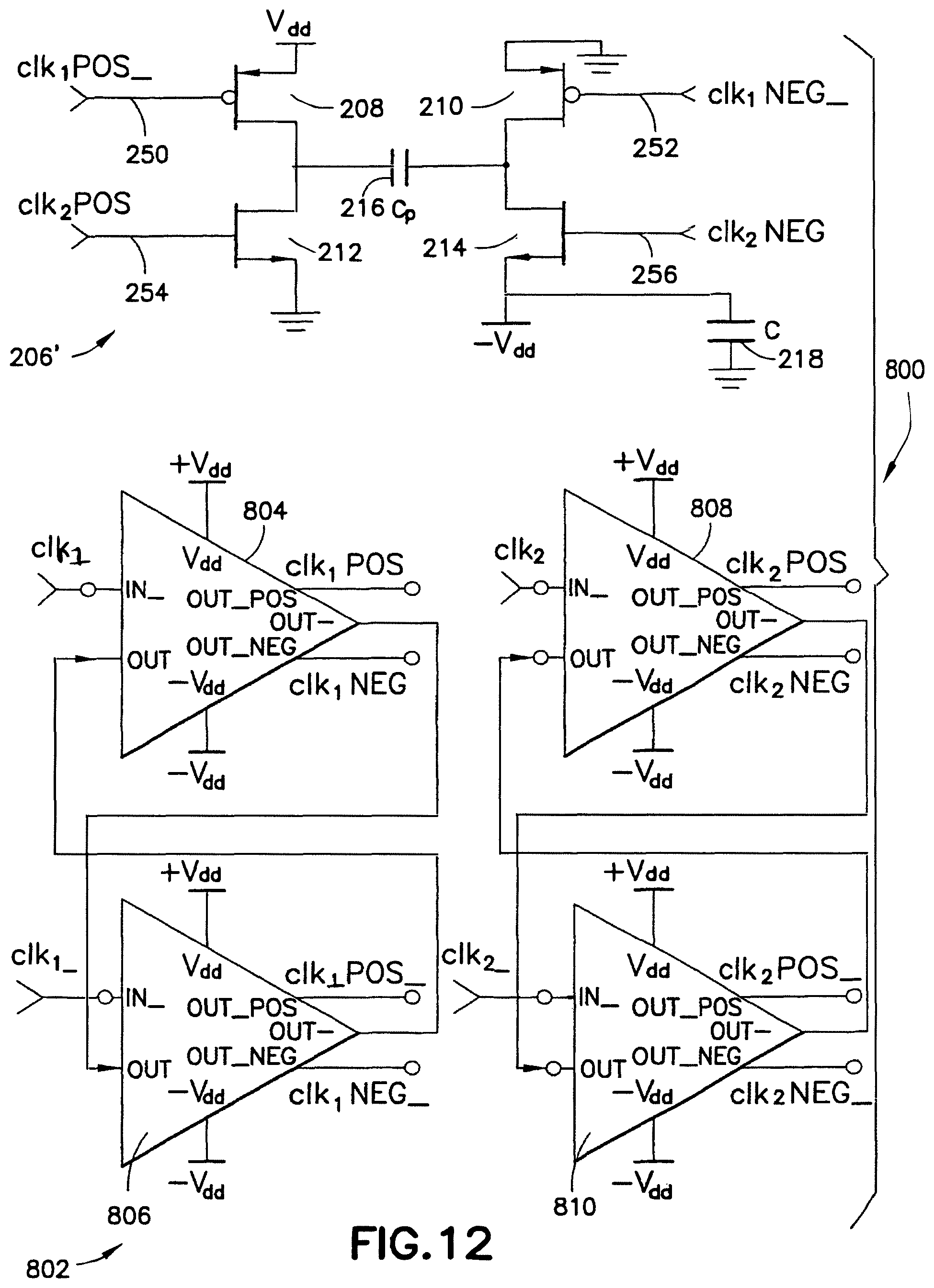
XML
uspto.report is an independent third-party trademark research tool that is not affiliated, endorsed, or sponsored by the United States Patent and Trademark Office (USPTO) or any other governmental organization. The information provided by uspto.report is based on publicly available data at the time of writing and is intended for informational purposes only.
While we strive to provide accurate and up-to-date information, we do not guarantee the accuracy, completeness, reliability, or suitability of the information displayed on this site. The use of this site is at your own risk. Any reliance you place on such information is therefore strictly at your own risk.
All official trademark data, including owner information, should be verified by visiting the official USPTO website at www.uspto.gov. This site is not intended to replace professional legal advice and should not be used as a substitute for consulting with a legal professional who is knowledgeable about trademark law.