System and methods for extracting correlation curves for an organic light emitting device
Chaji Sept
U.S. patent number 10,783,814 [Application Number 16/203,728] was granted by the patent office on 2020-09-22 for system and methods for extracting correlation curves for an organic light emitting device. This patent grant is currently assigned to Ignis Innovation Inc.. The grantee listed for this patent is Ignis Innovation Inc.. Invention is credited to Gholamreza Chaji.


| United States Patent | 10,783,814 |
| Chaji | September 22, 2020 |
System and methods for extracting correlation curves for an organic light emitting device
Abstract
A system determines the efficiency degradation of organic light emitting devices (OLEDs) in multiple array-based semiconductor devices having arrays of pixels that include OLEDs. The system determines the relationship between changes in an electrical operating parameter of the OLEDs and the efficiency degradation of the OLEDs in each of the array-based semiconductor devices, uses the determined relationship for a selected one of the array-based semiconductor devices to determine the efficiency degradation of the OLEDs, and compensates for the efficiency degradation. The relationship between changes in an electrical operating parameter of the OLEDs and the efficiency degradation of the OLEDs in the array-based semiconductor devices may be determined by the use of a test OLED associated with each of the devices.
| Inventors: | Chaji; Gholamreza (Waterloo, CA) | ||||||||||
|---|---|---|---|---|---|---|---|---|---|---|---|
| Applicant: |
|
||||||||||
| Assignee: | Ignis Innovation Inc.
(Waterloo, CA) |
||||||||||
| Family ID: | 1000005070437 | ||||||||||
| Appl. No.: | 16/203,728 | ||||||||||
| Filed: | November 29, 2018 |
Prior Publication Data
| Document Identifier | Publication Date | |
|---|---|---|
| US 20190096301 A1 | Mar 28, 2019 | |
Related U.S. Patent Documents
| Application Number | Filing Date | Patent Number | Issue Date | ||
|---|---|---|---|---|---|
| 14314514 | Jun 25, 2014 | 10176736 | |||
| 14286711 | Jan 30, 2018 | 9881532 | |||
| 14027811 | Aug 30, 2016 | 9430958 | |||
| 13020252 | Nov 19, 2013 | 8589100 | |||
Foreign Application Priority Data
| Feb 4, 2010 [CA] | 2692097 | |||
| Current U.S. Class: | 1/1 |
| Current CPC Class: | G09G 3/006 (20130101); G09G 3/3291 (20130101); G09G 3/3258 (20130101); G09G 3/32 (20130101); G09G 2300/0413 (20130101); G09G 2320/029 (20130101); G09G 2360/145 (20130101); G09G 2320/043 (20130101); G09G 2320/0285 (20130101) |
| Current International Class: | G09G 3/00 (20060101); G09G 3/32 (20160101); G09G 3/3291 (20160101); G09G 3/3258 (20160101) |
References Cited [Referenced By]
U.S. Patent Documents
| 7619597 | November 2009 | Nathan |
| 7656370 | February 2010 | Schneider |
| 10176736 | January 2019 | Chaji |
| 2008/0048951 | February 2008 | Naugler, Jr. |
| 2008/0174335 | July 2008 | Maekawa |
| 2009/0033598 | February 2009 | Suh |
Attorney, Agent or Firm: Stratford Managers Corporation
Parent Case Text
CROSS-REFERENCE TO RELATED APPLICATIONS
This application is a continuation of U.S. patent application Ser. No. 14/314,514, now allowed, which is a continuation-in-part of and claims priority to U.S. patent application Ser. No. 14/286,711, filed May 23, 2014, now U.S. Pat. No. 9,881,532, which is a continuation-in-part of U.S. patent application Ser. No. 14/027,811, filed Sep. 16, 2013, now U.S. Pat. No. 9,430,958, which is a continuation of U.S. patent application Ser. No. 13/020,252, filed Feb. 3, 2011, now U.S. Pat. No. 8,589,100, which claims priority to Canadian Application No. 2,692,097, filed Feb. 4, 2010, now abandoned, each of which is hereby incorporated by reference herein in its entirety.
Claims
The invention claimed is:
1. A method of determining the efficiency degradation of organic light emitting devices (OLEDs) and compensating for said deficiency an array-based semiconductor display device having an array of pixels that include OLEDs, the array-based semiconductor display device further comprising a controller and a readout circuit, said method comprising: storing a library of interdependency curves in a memory of the array-based semiconductor display device, said interdependency curves directly relating changes in an electrical operating parameter for one or more reference OLED pixels to the efficiency degradation of said one or more reference OLED pixels for a plurality of stress conditions; using the controller to: a) control the readout circuit to periodically measure the electrical operating parameter for at least one OLED in at least one of the pixels of the array-based semiconductor display device, determine changes in said electrical operating parameter from a baseline value, and store the changes in the memory; b) determine a stress condition of the at least one OLED using a calculated rate of change of the electrical operating parameter for the at least one OLED with use of said stored changes in said electrical operating parameter; c) determine the efficiency degradation of the at least one OLED based on at least one interdependency curve selected from the library with use of the determined stress condition, and d) modify a programming voltage or current for the at least one of the pixels to compensate for said efficiency degradation.
2. The method of claim 1, wherein the library comprises interdependency curves that are obtained by a controller measuring one or more test OLEDs in a similar display being similar to said array-based semiconductor display device using a readout circuit of the similar display and one or more optical sensors coupled to said one or more test OLEDs.
3. The method of claim 1, wherein the array of pixels of the array-based semiconductor display device is fabricated from a same substrate, the substrate further including one or more test OLED devices, the method comprising: using one or more photo sensors optically coupled to the one or more test OLED devices and a readout circuit electrically coupled to the one or more test OLED devices to obtain a set of interdependency curves for a set of different stress conditions, each of said interdependency curves directly relating changes in the electrical operating parameter of the one or more test OLED devices to the efficiency degradation thereof at one of the stress conditions, and storing the set of interdependency curves in the library of interdependency curves.
4. The method of claim 3 wherein the one or more photo sensors are comprised within said one or more test OLED devices.
5. The method of claim 3 comprising: i) measuring a test OLED comprised in said array-based semiconductor display, ii) identifying an interdependency curve from the library that has the closest aging behavior to said measured test OLED, iii) comparing the difference between the aging behaviors of said identified interdependency curve and said measured test OLED with a predetermined threshold, and iv) if said difference exceeds said threshold, using the test OLED to obtain a new interdependency curve and updating the library of interdependency curves stored with the display.
6. The method of claim 5 comprising, using said identified interdependency curve to compensate for the efficiency degradation of the display if said difference is less than said threshold.
7. The method of claim 1 in which the controller compares the rate of change and the changes determined in steps (a) and (b) to stored values thereof to determine the stress condition.
8. The method of claim 1, further comprising, measuring a test OLED comprised in said array-based semiconductor display device, generating an interdependency curve that corresponds to the measurements of said test OLED in said array-based semiconductor display device, and updating the library with the interdependency curve generated from the measurements of said test OLED.
Description
FIELD OF THE INVENTION
This invention is directed generally to displays that use light emissive devices such as OLEDs and, more particularly, to extracting characterization correlation curves under different stress conditions in such displays to compensate for aging of the light emissive devices.
BACKGROUND OF THE INVENTION
Active matrix organic light emitting device ("AMOLED") displays offer the advantages of lower power consumption, manufacturing flexibility, and faster refresh rate over conventional liquid crystal displays. In contrast to conventional liquid crystal displays, there is no backlighting in an AMOLED display as each pixel consists of different colored OLEDs emitting light independently. The OLEDs emit light based on current supplied through a drive transistor. The drive transistor is typically a thin film transistor (TFT). The power consumed in each pixel has a direct relation with the magnitude of the generated light in that pixel.
During operation of an organic light emitting diode device, it undergoes degradation, which causes light output at a constant current to decrease over time. The OLED device also undergoes an electrical degradation, which causes the current to drop at a constant bias voltage over time. These degradations are caused primarily by stress related to the magnitude and duration of the applied voltage on the OLED and the resulting current passing through the device. Such degradations are compounded by contributions from the environmental factors such as temperature, humidity, or presence of oxidants over time. The aging rate of the thin film transistor devices is also environmental and stress (bias) dependent. The aging of the drive transistor and the OLED may be properly determined via calibrating the pixel against stored historical data from the pixel at previous times to determine the aging effects on the pixel. Accurate aging data is therefore necessary throughout the lifetime of the display device.
In one compensation technique for OLED displays, the aging (and/or uniformity) of a panel of pixels is extracted and stored in lookup tables as raw or processed data. Then a compensation module uses the stored data to compensate for any shift in electrical and optical parameters of the OLED (e.g., the shift in the OLED operating voltage and the optical efficiency) and the backplane (e.g., the threshold voltage shift of the TFT), hence the programming voltage of each pixel is modified according to the stored data and the video content. The compensation module modifies the bias of the driving TFT in a way that the OLED passes enough current to maintain the same luminance level for each gray-scale level. In other words, a correct programming voltage properly offsets the electrical and optical aging of the OLED as well as the electrical degradation of the TFT.
The electrical parameters of the backplane TFTs and OLED devices are continuously monitored and extracted throughout the lifetime of the display by electrical feedback-based measurement circuits. Further, the optical aging parameters of the OLED devices are estimated from the OLED's electrical degradation data. However, the optical aging effect of the OLED is dependent on the stress conditions placed on individual pixels as well, and since the stresses vary from pixel to pixel, accurate compensation is not assured unless the compensation tailored for a specific stress level is determined.
There is therefore a need for efficient extraction of characterization correlation curves of the optical and electrical parameters that are accurate for stress conditions on active pixels for compensation for aging and other effects. There is also a need for having a variety of characterization correlation curves for a variety of stress conditions that the active pixels may be subjected to during operation of the display. There is a further need for accurate compensation systems for pixels in an organic light emitting device based display.
SUMMARY
In accordance with one embodiment, a system is provided for determining the efficiency degradation of organic light emitting devices (OLEDs) in multiple array-based semiconductor devices having arrays of pixels that include OLEDs. The system determines the relationship between changes in an electrical operating parameter of the OLEDs and the efficiency degradation of the OLEDs in each of the array-based semiconductor devices, uses the determined relationship for a selected one of the array-based semiconductor devices to determine the efficiency degradation of the OLEDs, and compensates for the efficiency degradation.
In one implementation, the relationship between changes in an electrical operating parameter of the OLEDs and the efficiency degradation of the OLEDs in the array-based semiconductor devices is determined by the use of a test OLED associated with each of the devices. The test OLED may be located on the substrate of the associated array-based semiconductor device, or in the semiconductor device itself. The determined relationship may be an OLED interdependency curve that relates an OLED electrical signal from the test OLED in a selected array-based semiconductor device with the efficiency degradation of that test OLED. The relationship may be determined at the time of fabrication of each of the array-based semiconductor devices, or during operation of the devices.
One embodiment uses a library of OLED interdependency curves that relate OLED electrical signals from test OLEDs in array-based semiconductor devices with the efficiency degradation of test OLEDs in the devices. The system measures a test OLED in a selected array-based semiconductor device, identifies an interdependency curve in the library that corresponds to the measurements of the test OLED in the selected array-based semiconductor device, and uses the identified interdependency curve to determine the aging behavior of the test OLED. The identified interdependency curve may be the curve in the library that has the closest aging behavior to the measured test OLED, and then the system compares the difference between the aging behaviors of the identified interdependency curve and the measured test OLED with a predetermined threshold, and if the difference exceeds the threshold, calculates a new interdependency curve and adding the new curve to the library. If the difference is less than the threshold, using the identified interdependency curve to compensate for the efficiency degradation of the display containing the measured test OLED
Additional aspects of the invention will be apparent to those of ordinary skill in the art in view of the detailed description of various embodiments, which is made with reference to the drawings, a brief description of which is provided below.
BRIEF DESCRIPTION OF THE DRAWINGS
The invention may best be understood by reference to the following description taken in conjunction with the accompanying drawings.
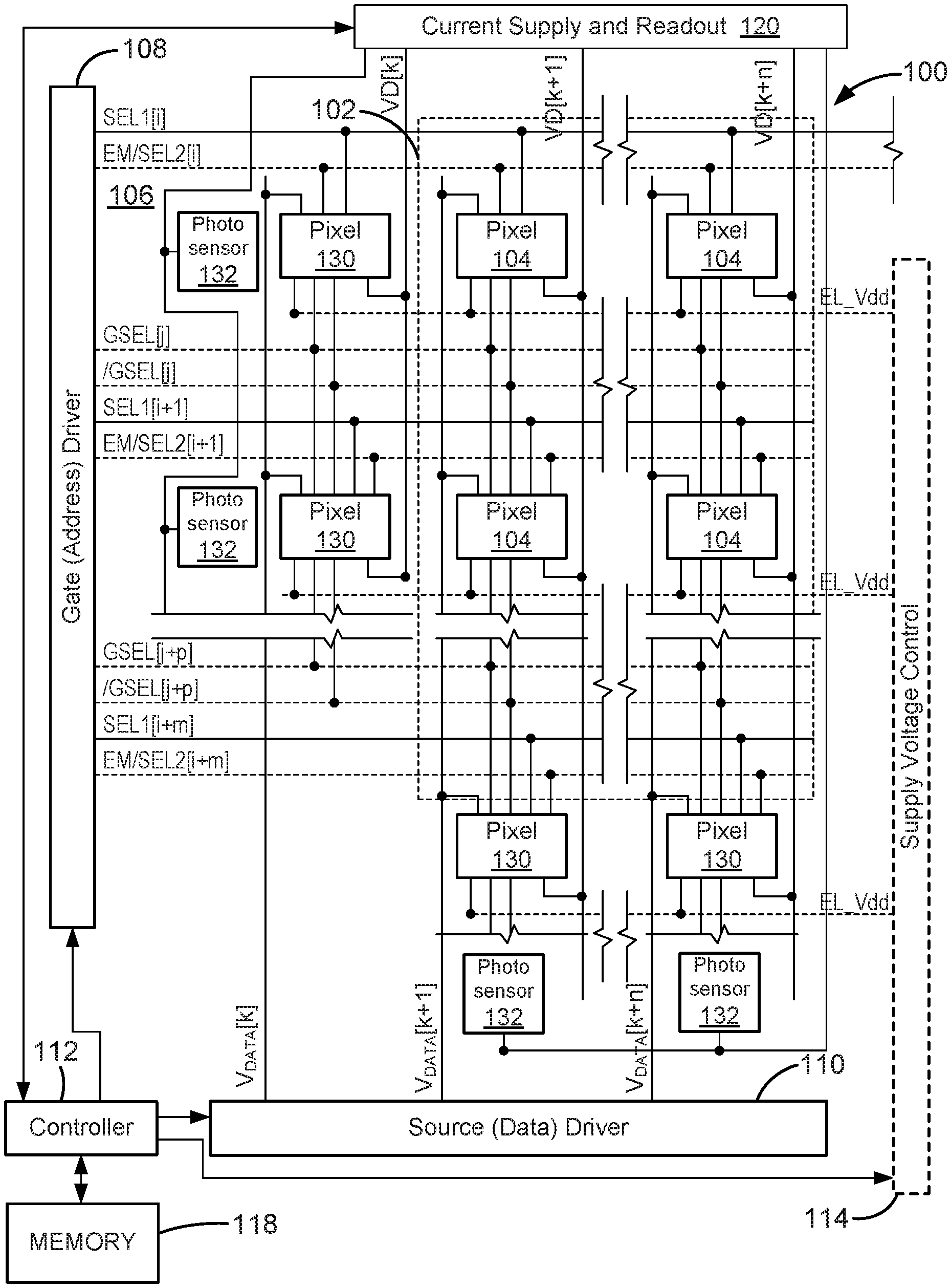
FIG. 1 is a block diagram of an AMOLED display system with compensation control;
FIG. 2 is a circuit diagram of one of the reference pixels in FIG. 1 for modifying characterization correlation curves based on the measured data;
FIG. 3 is a graph of luminance emitted from an active pixel reflecting the different levels of stress conditions over time that may require different compensation;
FIG. 4 is a graph of the plots of different characterization correlation curves and the results of techniques of using predetermined stress conditions to determine compensation;
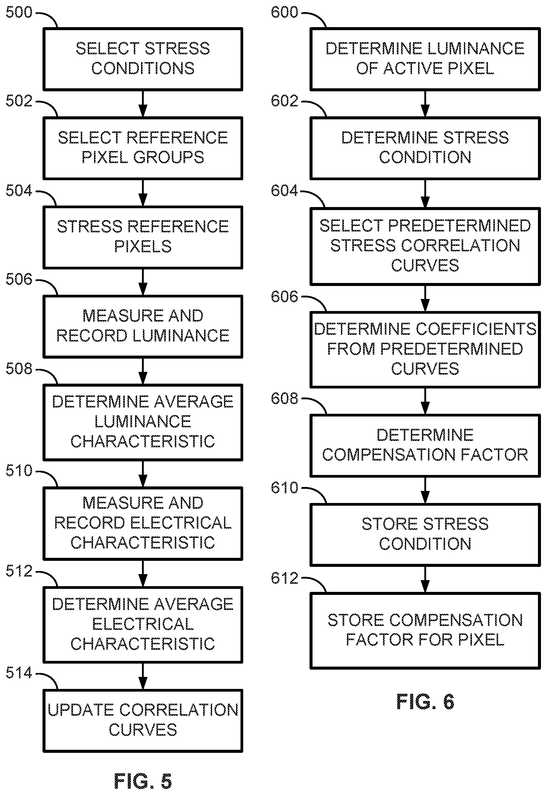
FIG. 5 is a flow diagram of the process of determining and updating characterization correlation curves based on groups of reference pixels under predetermined stress conditions; and
FIG. 6 is a flow diagram of the process of compensating the programming voltages of active pixels on a display using predetermined characterization correlation curves.
FIG. 7 is an interdependency curve of OLED efficiency degradation versus changes in OLED voltage.
FIG. 8 is a graph of OLED stress history versus stress intensity.
FIG. 9A is a graph of change in OLED voltage versus time for different stress conditions.
FIG. 9B is a graph of rate of change of OLED voltage versus time for different stress conditions.
FIG. 10 is a graph of rate of change of OLED voltage versus change in OLED voltage, for different stress conditions.
FIG. 11 is a flow chart of a procedure for extracting OLED efficiency degradation from changes in an OLED parameter such as OLED voltage.
FIG. 12 is an OLED interdependency curve relating an OLED electrical signal and efficiency degradation.
FIG. 13 is a flow chart of a procedure for extracting interdependency curves from test devices.
FIG. 14 is a flow chart of a procedure for calculating interdependency curves from a library.
While the invention is susceptible to various modifications and alternative forms, specific embodiments have been shown by way of example in the drawings and will be described in detail herein. It should be understood, however, that the invention is not intended to be limited to the particular forms disclosed. Rather, the invention is to cover all modifications, equivalents, and alternatives falling within the spirit and scope of the invention as defined by the appended claims.
DETAILED DESCRIPTION
FIG. 1 is an electronic display system 100 having an active matrix area or pixel array 102 in which an array of active pixels 104 are arranged in a row and column configuration. For ease of illustration, only two rows and columns are shown. External to the active matrix area, which is the pixel array 102, is a peripheral area 106 where peripheral circuitry for driving and controlling the area of the pixel array 102 are disposed. The peripheral circuitry includes a gate or address driver circuit 108, a source or data driver circuit 110, a controller 112, and an optional supply voltage (e.g., EL_Vdd) driver 114. The controller 112 controls the gate, source, and supply voltage drivers 108, 110, 114. The gate driver 108, under control of the controller 112, operates on address or select lines SEL[i], SEL[i+1], and so forth, one for each row of pixels 104 in the pixel array 102. In pixel sharing configurations described below, the gate or address driver circuit 108 can also optionally operate on global select lines GSEL[j] and optionally/GSEL[j], which operate on multiple rows of pixels 104 in the pixel array 102, such as every two rows of pixels 104. The source driver circuit 110, under control of the controller 112, operates on voltage data lines Vdata[k], Vdata[k+1], and so forth, one for each column of pixels 104 in the pixel array 102. The voltage data lines carry voltage programming information to each pixel 104 indicative of brightness of each light emitting device in the pixel 104. A storage element, such as a capacitor, in each pixel 104 stores the voltage programming information until an emission or driving cycle turns on the light emitting device. The optional supply voltage driver 114, under control of the controller 112, controls a supply voltage (EL_Vdd) line, one for each row of pixels 104 in the pixel array 102. The controller 112 is also coupled to a memory 118 that stores various characterization correlation curves and aging parameters of the pixels 104 as will be explained below. The memory 118 may be one or more of a flash memory, an SRAM, a DRAM, combinations thereof, and/or the like.
The display system 100 may also include a current source circuit, which supplies a fixed current on current bias lines. In some configurations, a reference current can be supplied to the current source circuit. In such configurations, a current source control controls the timing of the application of a bias current on the current bias lines. In configurations in which the reference current is not supplied to the current source circuit, a current source address driver controls the timing of the application of a bias current on the current bias lines.
As is known, each pixel 104 in the display system 100 needs to be programmed with information indicating the brightness of the light emitting device in the pixel 104. A frame defines the time period that includes a programming cycle or phase during which each and every pixel in the display system 100 is programmed with a programming voltage indicative of a brightness and a driving or emission cycle or phase during which each light emitting device in each pixel is turned on to emit light at a brightness commensurate with the programming voltage stored in a storage element. A frame is thus one of many still images that compose a complete moving picture displayed on the display system 100. There are at least two schemes for programming and driving the pixels: row-by-row, or frame-by-frame. In row-by-row programming, a row of pixels is programmed and then driven before the next row of pixels is programmed and driven. In frame-by-frame programming, all rows of pixels in the display system 100 are programmed first, and all of the frames are driven row-by-row. Either scheme can employ a brief vertical blanking time at the beginning or end of each period during which the pixels are neither programmed nor driven.
The components located outside of the pixel array 102 may be disposed in a peripheral area 106 around the pixel array 102 on the same physical substrate on which the pixel array 102 is disposed. These components include the gate driver 108, the source driver 110, and the optional supply voltage control 114. Alternately, some of the components in the peripheral area can be disposed on the same substrate as the pixel array 102 while other components are disposed on a different substrate, or all of the components in the peripheral area can be disposed on a substrate different from the substrate on which the pixel array 102 is disposed. Together, the gate driver 108, the source driver 110, and the supply voltage control 114 make up a display driver circuit. The display driver circuit in some configurations may include the gate driver 108 and the source driver 110 but not the supply voltage control 114.
The display system 100 further includes a current supply and readout circuit 120, which reads output data from data output lines, VD [k], VD [k+1], and so forth, one for each column of active pixels 104 in the pixel array 102. A set of optional reference devices such as reference pixels 130 is fabricated on the edge of the pixel array 102 outside the active pixels 104 in the peripheral area 106. The reference pixels 130 also may receive input signals from the controller 112 and may output data signals to the current supply and readout circuit 120. The reference pixels 130 include the drive transistor and an OLED but are not part of the pixel array 102 that displays images. As will be explained below, different groups of reference pixels 130 are placed under different stress conditions via different current levels from the current supply circuit 120. Because the reference pixels 130 are not part of the pixel array 102 and thus do not display images, the reference pixels 130 may provide data indicating the effects of aging at different stress conditions. Although only one row and column of reference pixels 130 is shown in FIG. 1, it is to be understood that there may be any number of reference pixels. Each of the reference pixels 130 in the example shown in FIG. 1 are fabricated next to a corresponding photo sensor 132. The photo sensor 132 is used to determine the luminance level emitted by the corresponding reference pixel 130. It is to be understood that reference devices such as the reference pixels 130 may be a stand alone device rather than being fabricated on the display with the active pixels 104.
FIG. 2 shows one example of a driver circuit 200 for one of the example reference pixels 130 in FIG. 1. The driver circuit 200 of the reference pixel 130 includes a drive transistor 202, an organic light emitting device ("OLED") 204, a storage capacitor 206, a select transistor 208 and a monitoring transistor 210. A voltage source 212 is coupled to the drive transistor 202. As shown in FIG. 2, the drive transistor 202 is a thin film transistor in this example that is fabricated from amorphous silicon. A select line 214 is coupled to the select transistor 208 to activate the driver circuit 200. A voltage programming input line 216 allows a programming voltage to be applied to the drive transistor 202. A monitoring line 218 allows outputs of the OLED 204 and/or the drive transistor 202 to be monitored. The select line 214 is coupled to the select transistor 208 and the monitoring transistor 210. During the readout time, the select line 214 is pulled high. A programming voltage may be applied via the programming voltage input line 216. A monitoring voltage may be read from the monitoring line 218 that is coupled to the monitoring transistor 210. The signal to the select line 214 may be sent in parallel with the pixel programming cycle.
The reference pixel 130 may be stressed at a certain current level by applying a constant voltage to the programming voltage input line 216. As will be explained below, the voltage output measured from the monitoring line 218 based on a reference voltage applied to the programming voltage input line 216 allows the determination of electrical characterization data for the applied stress conditions over the time of operation of the reference pixel 130. Alternatively, the monitor line 218 and the programming voltage input line 216 may be merged into one line (i.e., Data/Mon) to carry out both the programming and monitoring functions through that single line. The output of the photo-sensor 132 allows the determination of optical characterization data for stress conditions over the time of operation for the reference pixel 130.
The display system 100 in FIG. 1, according to one exemplary embodiment, in which the brightness of each pixel (or subpixel) is adjusted based on the aging of at least one of the pixels, to maintain a substantially uniform display over the operating life of the system (e.g., 75,000 hours). Non-limiting examples of display devices incorporating the display system 100 include a mobile phone, a digital camera, a personal digital assistant (PDA), a computer, a television, a portable video player, a global positioning system (GPS), etc.
As the OLED material of an active pixel 104 ages, the voltage required to maintain a constant current for a given level through the OLED increases. To compensate for electrical aging of the OLEDs, the memory 118 stores the required compensation voltage of each active pixel to maintain a constant current. It also stores data in the form of characterization correlation curves for different stress conditions that is utilized by the controller 112 to determine compensation voltages to modify the programming voltages to drive each OLED of the active pixels 104 to correctly display a desired output level of luminance by increasing the OLED's current to compensate for the optical aging of the OLED. In particular, the memory 118 stores a plurality of predefined characterization correlation curves or functions, which represent the degradation in luminance efficiency for OLEDs operating under different predetermined stress conditions. The different predetermined stress conditions generally represent different types of stress or operating conditions that an active pixel 104 may undergo during the lifetime of the pixel. Different stress conditions may include constant current requirements at different levels from low to high, constant luminance requirements from low to high, or a mix of two or more stress levels. For example, the stress levels may be at a certain current for some percentage of the time and another current level for another percentage of the time. Other stress levels may be specialized such as a level representing an average streaming video displayed on the display system 100. Initially, the base line electrical and optical characteristics of the reference devices such as the reference pixels 130 at different stress conditions are stored in the memory 118. In this example, the baseline optical characteristic and the baseline electrical characteristic of the reference device are measured from the reference device immediately after fabrication of the reference device.
Each such stress condition may be applied to a group of reference pixels such as the reference pixels 130 by maintaining a constant current through the reference pixel 130 over a period of time, maintaining a constant luminance of the reference pixel 130 over a period of time, and/or varying the current through or luminance of the reference pixel at different predetermined levels and predetermined intervals over a period of time. The current or luminance level(s) generated in the reference pixel 130 can be, for example, high values, low values, and/or average values expected for the particular application for which the display system 100 is intended. For example, applications such as a computer monitor require high values. Similarly, the period(s) of time for which the current or luminance level(s) are generated in the reference pixel may depend on the particular application for which the display system 100 is intended.
It is contemplated that the different predetermined stress conditions are applied to different reference pixels 130 during the operation of the display system 100 in order to replicate aging effects under each of the predetermined stress conditions. In other words, a first predetermined stress condition is applied to a first set of reference pixels, a second predetermined stress condition is applied to a second set of reference pixels, and so on. In this example, the display system 100 has groups of reference pixels 130 that are stressed under 16 different stress conditions that range from a low current value to a high current value for the pixels. Thus, there are 16 different groups of reference pixels 130 in this example. Of course, greater or lesser numbers of stress conditions may be applied depending on factors such as the desired accuracy of the compensation, the physical space in the peripheral area 106, the amount of processing power available, and the amount of memory for storing the characterization correlation curve data.
By continually subjecting a reference pixel or group of reference pixels to a stress condition, the components of the reference pixel are aged according to the operating conditions of the stress condition. As the stress condition is applied to the reference pixel during the operation of the system 100, the electrical and optical characteristics of the reference pixel are measured and evaluated to determine data for determining correction curves for the compensation of aging in the active pixels 104 in the array 102. In this example, the optical characteristics and electrical characteristics are measured once an hour for each group of reference pixels 130. The corresponding characteristic correlation curves are therefore updated for the measured characteristics of the reference pixels 130. Of course, these measurements may be made in shorter periods of time or for longer periods of time depending on the accuracy desired for aging compensation.
Generally, the luminance of the OLED 204 has a direct linear relationship with the current applied to the OLED 204. The optical characteristic of an OLED may be expressed as: L=O*I In this equation, luminance, L, is a result of a coefficient, O, based on the properties of the OLED multiplied by the current I. As the OLED 204 ages, the coefficient O decreases and therefore the luminance decreases for a constant current value. The measured luminance at a given current may therefore be used to determine the characteristic change in the coefficient, O, due to aging for a particular OLED 204 at a particular time for a predetermined stress condition.
The measured electrical characteristic represents the relationship between the voltage provided to the drive transistor 202 and the resulting current through the OLED 204. For example, the change in voltage required to achieve a constant current level through the OLED of the reference pixel may be measured with a voltage sensor or thin film transistor such as the monitoring transistor 210 in FIG. 2. The required voltage generally increases as the OLED 204 and drive transistor 202 ages. The required voltage has a power law relation with the output current as shown in the following equation I=k*(V-e).sup.a In this equation, the current is determined by a constant, k, multiplied by the input voltage, V, minus a coefficient, e, which represents the electrical characteristics of the drive transistor 202. The voltage therefore has a power law relation by the variable, a, to the current, I. As the transistor 202 ages, the coefficient, e, increases thereby requiring greater voltage to produce the same current. The measured current from the reference pixel may therefore be used to determine the value of the coefficient, e, for a particular reference pixel at a certain time for the stress condition applied to the reference pixel.
As explained above, the optical characteristic, O, represents the relationship between the luminance generated by the OLED 204 of the reference pixel 130 as measured by the photo sensor 132 and the current through the OLED 204 in FIG. 2. The measured electrical characteristic, e, represents the relationship between the voltage applied and the resulting current. The change in luminance of the reference pixel 130 at a constant current level from a baseline optical characteristic may be measured by a photo sensor such as the photo sensor 132 in FIG. 1 as the stress condition is applied to the reference pixel. The change in electric characteristics, e, from a baseline electrical characteristic may be measured from the monitoring line to determine the current output. During the operation of the display system 100, the stress condition current level is continuously applied to the reference pixel 130. When a measurement is desired, the stress condition current is removed and the select line 214 is activated. A reference voltage is applied and the resulting luminance level is taken from the output of the photo sensor 132 and the output voltage is measured from the monitoring line 218. The resulting data is compared with previous optical and electrical data to determine changes in current and luminance outputs for a particular stress condition from aging to update the characteristics of the reference pixel at the stress condition. The updated characteristics data is used to update the characteristic correlation curve.
Then by using the electrical and optical characteristics measured from the reference pixel, a characterization correlation curve (or function) is determined for the predetermined stress condition over time. The characterization correlation curve provides a quantifiable relationship between the optical degradation and the electrical aging expected for a given pixel operating under the stress condition. More particularly, each point on the characterization correlation curve determines the correlation between the electrical and optical characteristics of an OLED of a given pixel under the stress condition at a given time where measurements are taken from the reference pixel 130. The characteristics may then be used by the controller 112 to determine appropriate compensation voltages for active pixels 104 that have been aged under the same stress conditions as applied to the reference pixels 130. In another example, the baseline optical characteristic may be periodically measured from a base OLED device at the same time as the optical characteristic of the OLED of the reference pixel is being measured. The base OLED device either is not being stressed or being stressed on a known and controlled rate. This will eliminate any environmental effect on the reference OLED characterization.
Due to manufacturing processes and other factors known to those skilled in the art, each reference pixel 130 of the display system 100 may not have uniform characteristics, resulting in different emitting performances. One technique is to average the values for the electrical characteristics and the values of the luminance characteristics obtained by a set of reference pixels under a predetermined stress condition. A better representation of the effect of the stress condition on an average pixel is obtained by applying the stress condition to a set of the reference pixels 130 and applying a polling-averaging technique to avoid defects, measurement noise, and other issues that can arise during application of the stress condition to the reference pixels. For example, faulty values such as those determined due to noise or a dead reference pixel may be removed from the averaging. Such a technique may have predetermined levels of luminance and electrical characteristics that must be met before inclusion of those values in the averaging. Additional statistical regression techniques may also be utilized to provide less weight to electrical and optical characteristic values that are significantly different from the other measured values for the reference pixels under a given stress condition.
In this example, each of the stress conditions is applied to a different set of reference pixels. The optical and electrical characteristics of the reference pixels are measured, and a polling-averaging technique and/or a statistical regression technique are applied to determine different characterization correlation curves corresponding to each of the stress conditions. The different characterization correlation curves are stored in the memory 118. Although this example uses reference devices to determine the correlation curves, the correlation curves may be determined in other ways such as from historical data or predetermined by a manufacturer.
During the operation of the display system 100, each group of the reference pixels 130 may be subjected to the respective stress conditions and the characterization correlation curves initially stored in the memory 118 may be updated by the controller 112 to reflect data taken from the reference pixels 130 that are subject to the same external conditions as the active pixels 104. The characterization correlation curves may thus be tuned for each of the active pixels 104 based on measurements made for the electrical and luminance characteristics of the reference pixels 130 during operation of the display system 100. The electrical and luminance characteristics for each stress condition are therefore stored in the memory 118 and updated during the operation of the display system 100. The storage of the data may be in a piecewise linear model. In this example, such a piecewise linear model has 16 coefficients that are updated as the reference pixels 130 are measured for voltage and luminance characteristics. Alternatively, a curve may be determined and updated using linear regression or by storing data in a look up table in the memory 118.
To generate and store a characterization correlation curve for every possible stress condition would be impractical due to the large amount of resources (e.g., memory storage, processing power, etc.) that would be required. The disclosed display system 100 overcomes such limitations by determining and storing a discrete number of characterization correlation curves at predetermined stress conditions and subsequently combining those predefined characterization correlation curves using linear or nonlinear algorithm(s) to synthesize a compensation factor for each pixel 104 of the display system 100 depending on the particular operating condition of each pixel. As explained above, in this example there are a range of 16 different predetermined stress conditions and therefore 16 different characterization correlation curves stored in the memory 118.
For each pixel 104, the display system 100 analyzes the stress condition being applied to the pixel 104, and determines a compensation factor using an algorithm based on the predefined characterization correlation curves and the measured electrical aging of the panel pixels. The display system 100 then provides a voltage to the pixel based on the compensation factor. The controller 112 therefore determines the stress of a particular pixel 104 and determines the closest two predetermined stress conditions and attendant characteristic data obtained from the reference pixels 130 at those predetermined stress conditions for the stress condition of the particular pixel 104. The stress condition of the active pixel 104 therefore falls between a low predetermined stress condition and a high predetermined stress condition.
The following examples of linear and nonlinear equations for combining characterization correlation curves are described in terms of two such predefined characterization correlation curves for ease of disclosure; however, it is to be understood that any other number of predefined characterization correlation curves can be utilized in the exemplary techniques for combining the characterization correlation curves. The two exemplary characterization correlation curves include a first characterization correlation curve determined for a high stress condition and a second characterization correlation curve determined for a low stress condition.
The ability to use different characterization correlation curves over different levels provides accurate compensation for active pixels 104 that are subjected to different stress conditions than the predetermined stress conditions applied to the reference pixels 130. FIG. 3 is a graph showing different stress conditions over time for an active pixel 104 that shows luminance levels emitted over time. During a first time period, the luminance of the active pixel is represented by trace 302, which shows that the luminance is between 300 and 500 nits (cd/cm.sup.2). The stress condition applied to the active pixel during the trace 302 is therefore relatively high. In a second time period, the luminance of the active pixel is represented by a trace 304, which shows that the luminance is between 300 and 100 nits. The stress condition during the trace 304 is therefore lower than that of the first time period and the age effects of the pixel during this time differ from the higher stress condition. In a third time period, the luminance of the active pixel is represented by a trace 306, which shows that the luminance is between 100 and 0 nits. The stress condition during this period is lower than that of the second period. In a fourth time period, the luminance of the active pixel is represented by a trace 308 showing a return to a higher stress condition based on a higher luminance between 400 and 500 nits.
The limited number of reference pixels 130 and corresponding limited numbers of stress conditions may require the use of averaging or continuous (moving) averaging for the specific stress condition of each active pixel 104. The specific stress conditions may be mapped for each pixel as a linear combination of characteristic correlation curves from several reference pixels 130. The combinations of two characteristic curves at predetermined stress conditions allow accurate compensation for all stress conditions occurring between such stress conditions. For example, the two reference characterization correlation curves for high and low stress conditions allow a close characterization correlation curve for an active pixel having a stress condition between the two reference curves to be determined. The first and second reference characterization correlation curves stored in the memory 118 are combined by the controller 112 using a weighted moving average algorithm. A stress condition at a certain time St (t.sub.i) for an active pixel may be represented by: St(t.sub.i)=(St(t.sub.i-1)*k.sub.avg+L(t.sub.i))/(k.sub.avg+1) In this equation, St(t.sub.i-1) is the stress condition at a previous time, k.sub.avg is a moving average constant. L(t.sub.i) is the measured luminance of the active pixel at the certain time, which may be determined by:
.function..function..gamma. ##EQU00001## In this equation, L.sub.peak is the highest luminance permitted by the design of the display system 100. The variable, g(t.sub.i) is the grayscale at the time of measurement, g.sub.peak is the highest grayscale value of use (e.g. 255) and .gamma. is a gamma constant. A weighted moving average algorithm using the characterization correlation curves of the predetermined high and low stress conditions may determine the compensation factor, K.sub.comp via the following equation: K.sub.comp=K.sub.highf.sub.high(.DELTA.I)+K.sub.lowf.sub.low(.DELTA.I) In this equation, f.sub.high is the first function corresponding to the characterization correlation curve for a high predetermined stress condition and f.sub.low is the second function corresponding to the characterization correlation curve for a low predetermined stress condition. .DELTA.I is the change in the current in the OLED for a fixed voltage input, which shows the change (electrical degradation) due to aging effects measured at a particular time. It is to be understood that the change in current may be replaced by a change in voltage, .DELTA.V, for a fixed current. K.sub.high is the weighted variable assigned to the characterization correlation curve for the high stress condition and K.sub.low is the weight assigned to the characterization correlation curve for the low stress condition. The weighted variables K.sub.high and K.sub.low may be determined from the following equations: K.sub.high=St(t.sub.i)/L.sub.high K.sub.low=1-K.sub.high Where L.sub.high is the luminance that was associated with the high stress condition.
The change in voltage or current in the active pixel at any time during operation represents the electrical characteristic while the change in current as part of the function for the high or low stress condition represents the optical characteristic. In this example, the luminance at the high stress condition, the peak luminance, and the average compensation factor (function of difference between the two characterization correlation curves), K.sub.avg, are stored in the memory 118 for determining the compensation factors for each of the active pixels. Additional variables are stored in the memory 118 including, but not limited to, the grayscale value for the maximum luminance permitted for the display system 100 (e.g., grayscale value of 255). Additionally, the average compensation factor, K.sub.avg, may be empirically determined from the data obtained during the application of stress conditions to the reference pixels.
As such, the relationship between the optical degradation and the electrical aging of any pixel 104 in the display system 100 may be tuned to avoid errors associated with divergence in the characterization correlation curves due to different stress conditions. The number of characterization correlation curves stored may also be minimized to a number providing confidence that the averaging technique will be sufficiently accurate for required compensation levels.
The compensation factor, K.sub.comp can be used for compensation of the OLED optical efficiency aging for adjusting programming voltages for the active pixel. Another technique for determining the appropriate compensation factor for a stress condition on an active pixel may be termed dynamic moving averaging. The dynamic moving averaging technique involves changing the moving average coefficient, K.sub.avg, during the lifetime of the display system 100 to compensate between the divergence in two characterization correlation curves at different predetermined stress conditions in order to prevent distortions in the display output. As the OLEDs of the active pixels age, the divergence between two characterization correlation curves at different stress conditions increases. Thus, K.sub.avg may be increased during the lifetime of the display system 100 to avoid a sharp transition between the two curves for an active pixel having a stress condition falling between the two predetermined stress conditions. The measured change in current, .DELTA.I, may be used to adjust the K.sub.avg value to improve the performance of the algorithm to determine the compensation factor.
Another technique to improve performance of the compensation process termed event-based moving averaging is to reset the system after each aging step. This technique further improves the extraction of the characterization correlation curves for the OLEDs of each of the active pixels 104. The display system 100 is reset after every aging step (or after a user turns on or off the display system 100). In this example, the compensation factor, K.sub.comp is determined by K.sub.comp=K.sub.comp_evt+K.sub.high(f.sub.high(.DELTA.I)-f.sub.high(.DEL- TA.I.sub.evt))+K.sub.low(f.sub.low(.DELTA.I)-f.sub.low(.DELTA.I.sub.evt)) In this equation, K.sub.comp_evt is the compensation factor calculated at a previous time, and .DELTA.I.sub.evt is the change in the OLED current during the previous time at a fixed voltage. As with the other compensation determination technique, the change in current may be replaced with the change in an OLED voltage change under a fixed current.
FIG. 4 is a graph 400 showing the different characterization correlation curves based on the different techniques. The graph 400 compares the change in the optical compensation percent and the change in the voltage of the OLED of the active pixel required to produce a given current. As shown in the graph 400, a high stress predetermined characterization correlation curve 402 diverges from a low stress predetermined characterization correlation curve 404 at greater changes in voltage reflecting aging of an active pixel. A set of points 406 represents the correction curve determined by the moving average technique from the predetermined characterization correlation curves 402 and 404 for the current compensation of an active pixel at different changes in voltage. As the change in voltage increases reflecting aging, the transition of the correction curve 406 has a sharp transition between the low characterization correlation curve 404 and the high characterization correlation curve 402. A set of points 408 represents the characterization correlation curve determined by the dynamic moving averaging technique. A set of points 410 represents the compensation factors determined by the event-based moving averaging technique. Based on OLED behavior, one of the above techniques can be used to improve the compensation for OLED efficiency degradation.
As explained above, an electrical characteristic of a first set of sample pixels is measured. For example, the electrical characteristic of each of the first set of sample pixels can be measured by a thin film transistor (TFT) connected to each pixel. Alternatively, for example, an optical characteristic (e.g., luminance) can be measured by a photo sensor provided to each of the first set of sample pixels. The amount of change required in the brightness of each pixel can be extracted from the shift in voltage of one or more of the pixels. This may be implemented by a series of calculations to determine the correlation between shifts in the voltage or current supplied to a pixel and/or the brightness of the light-emitting material in that pixel.
The above described methods of extracting characteristic correlation curves for compensating aging of the pixels in the array may be performed by a processing device such as the controller 112 in FIG. 1 or another such device, which may be conveniently implemented using one or more general purpose computer systems, microprocessors, digital signal processors, micro-controllers, application specific integrated circuits (ASIC), programmable logic devices (PLD), field programmable logic devices (FPLD), field programmable gate arrays (FPGA) and the like, programmed according to the teachings as described and illustrated herein, as will be appreciated by those skilled in the computer, software, and networking arts.
In addition, two or more computing systems or devices may be substituted for any one of the controllers described herein. Accordingly, principles and advantages of distributed processing, such as redundancy, replication, and the like, also can be implemented, as desired, to increase the robustness and performance of controllers described herein.
The operation of the example characteristic correlation curves for compensating aging methods may be performed by machine readable instructions. In these examples, the machine readable instructions comprise an algorithm for execution by: (a) a processor, (b) a controller, and/or (c) one or more other suitable processing device(s). The algorithm may be embodied in software stored on tangible media such as, for example, a flash memory, a CD-ROM, a floppy disk, a hard drive, a digital video (versatile) disk (DVD), or other memory devices, but persons of ordinary skill in the art will readily appreciate that the entire algorithm and/or parts thereof could alternatively be executed by a device other than a processor and/or embodied in firmware or dedicated hardware in a well-known manner (e.g., it may be implemented by an application specific integrated circuit (ASIC), a programmable logic device (PLD), a field programmable logic device (FPLD), a field programmable gate array (FPGA), discrete logic, etc.). For example, any or all of the components of the characteristic correlation curves for compensating aging methods could be implemented by software, hardware, and/or firmware. Also, some or all of the machine readable instructions represented may be implemented manually.
FIG. 5 is a flow diagram of a process to determine and update the characterization correlation curves for a display system such as the display system 100 in FIG. 1. A selection of stress conditions is made to provide sufficient baselines for correlating the range of stress conditions for the active pixels (500). A group of reference pixels is then selected for each of the stress conditions (502). The reference pixels for each of the groups corresponding to each of the stress conditions are then stressed at the corresponding stress condition and base line optical and electrical characteristics are stored (504). At periodic intervals the luminance levels are measured and recorded for each pixel in each of the groups (506). The luminance characteristic is then determined by averaging the measured luminance for each pixel in the group of the pixels for each of the stress conditions (508). The electrical characteristics for each of the pixels in each of the groups are determined (510). The average of each pixel in the group is determined to determine the average electrical characteristic (512). The average luminance characteristic and the average electrical characteristic for each group are then used to update the characterization correlation curve for the corresponding predetermined stress condition (514). Once the correlation curves are determined and updated, the controller may use the updated characterization correlation curves to compensate for aging effects for active pixels subjected to different stress conditions.
Referring to FIG. 6, a flowchart is illustrated for a process of using appropriate predetermined characterization correlation curves for a display system 100 as obtained in the process in FIG. 5 to determine the compensation factor for an active pixel at a given time. The luminance emitted by the active pixel is determined based on the highest luminance and the programming voltage (600). A stress condition is measured for a particular active pixel based on the previous stress condition, determined luminance, and the average compensation factor (602). The appropriate predetermined stress characterization correlation curves are read from memory (604). In this example, the two characterization correlation curves correspond to predetermined stress conditions that the measured stress condition of the active pixel falls between. The controller 112 then determines the coefficients from each of the predetermined stress conditions by using the measured current or voltage change from the active pixel (606). The controller then determines a modified coefficient to calculate a compensation voltage to add to the programming voltage to the active pixels (608). The determined stress condition is stored in the memory (610). The controller 112 then stores the new compensation factor, which may then be applied to modify the programming voltages to the active pixel during each frame period after the measurements of the reference pixels 130 (612).
OLED efficiency degradation can be calculated based on an interdependency curve based on OLED electrical changes versus efficiency degradation, such as the interdependency curve in FIG. 7. Here, the change in the OLED electrical parameter is detected, and that value is used to extract the efficiency degradation from the curve. The pixel current can then be adjusted accordingly to compensate for the degradation. The main challenge is that the interdependency curve is a function of stress conditions. Therefore, to achieve more accurate compensation, one needs to consider the effect of different stress conditions. One method is to use the stress condition of each pixel (or a group of pixels) to select from among different interdependency curves, to extract the proper efficiency lost for each specific case. Several methods of determining the stress condition will now be described.
First, one can create a stress history for each pixel (or group of pixels). The stress history can be simply a moving average of the stress conditions. To improve the calculation accuracy, a weighted stress history can be used. Here, the effect of each stress can have a different weight based on stress intensity or period, as in the example depicted in FIG. 8. For example, the effect of low intensity stress is less on selecting the OLED interdependency curve. Therefore, a curve that has lower weight for small intensity can be used, such as the curve in FIG. 8. Sub-sampling can also be used to calculate the stress history, to reduce the memory transfer activities. In one case, one can assume the stress history is low frequency in time. In this case, there is no need to sample the pixel conditions for every frame. The sampling rate can be modified for different applications based on content frame rate. Here, during every frame only a few pixels can be selected to obtain an updated stress history.
In another case, one can assume the stress history is low frequency in space. In this case, there is no need to sample all the pixels. Here, a sub-set of pixels are used to calculate the stress history, and then an interpolation technique can be used to calculate the stress history for all the pixels.
In another case, one can combine both low sampling rates in time and space.
In some cases, including the memory and calculation block required for stress history may not be possible. Here, the rate of change in the OLED electrical parameter can be used to extract the stress conditions, as depicted in FIGS. 9A and 9B. FIG. 9A illustrates the change of .DELTA.V.sub.OLED with time, for low, medium and high stress conditions, and FIG. 9B illustrates the rate of change versus time for the same three stress conditions.
As illustrated in FIG. 10, the rate of change in the electrical parameter can be used as an indicator of stress conditions. For example, the rate of change in the electrical parameter based on the change in the electrical parameter may be modeled or experimentally extracted for different stress conditions, as depicted in FIG. 10. The rate of change may also be used to extract the stress condition based on comparing the measured change and rate of change in the electrical parameter. Here, the function developed for change and rate of change of the electrical parameter is used. Alternatively, the stress condition, interdependency curves, and measured changed parameter may be used.
FIG. 11 is a flow chart of a procedure for compensating the OLED efficiency degradation based on measuring the change and rate of change in the electrical parameter of the OLED. In this procedure, the change in the OLED parameter (e.g., OLED voltage) is extracted in step 1101, and then the rate of change in the OLED parameter, based on previously extracted values, is calculated in step 1102. Step 1103 then uses the rate of change and the change in the parameter to identify the stress condition. Finally, step 1104 calculates the efficiency degradation from the stress condition, the measured parameter, and interdependency curves.
One can compensate for OLED efficiency degradation using interdependency curves relating OLED electrical change (current or voltage) and efficiency degradation, as depicted in FIG. 12. Due to process variations, the interdependency curve may vary. In one example, a test OLED can be used in each display and the curve extracted for each display after fabrication or during the display operation. In the case of smaller displays, the test OLED devices can be put on the substrates and used to extract the curves after fabrication.
FIG. 13 is a flow chart of a process for extracting the interdependency curves from the test devices, either off line or during the display operation, or a combination of both. In this case, the curves extracted in the factory are stored for aging compensation. During the display operation, the curve can be updated with additional data based on measurement results of the test device in the display. However, since extraction may take time, a set of curves may measured in advance and put in the library. Here, the test devices are aged at predetermined aging levels (generally higher than normal) to extract some aging behavior in a short time period (and/or their current-voltage-luminance, IVL, is measured). After that, the extracted aging behavior is used to find a proper curve, having a similar or close aging behavior, from the library of curves.
In FIG. 13, the first step 1301 adds the test device on the substrate, in or out of the display area. Then step 1302 measures the test device to extract the interdependency curves. Step 1303 calculates the interdependency curves for the displays on the substrate, based on the measured curves. The curves are stored for each display in step 1304, and then used for compensating the display aging in step 1305. Alternatively, the test devices can be measured during the display operation at step 1306. Step 1307 then updates the interdependence curves based on the measured results. Step 1308 extrapolates the curves if needed, and step 1309 compensates the display based on the curves.
The following are some examples of procedures for finding a proper curve from a library: (1) Choose the one with closest aging behavior (and/or IVL characteristic). (2) Use the samples in the library with the closer behavior to the test sample and create a curve for the display. Here, weighted averaging can be used in which the weight of each curve is determined based on the error between their aging behaviors. (3) If the error between the closet set of curves in the library and the test device is higher than a predetermined threshold, the test device can be used to create new curves and add them to the library.
FIG. 14 is a flow chart of a procedure for addressing the process variation between substrates or within a substrate. The first step 1401 adds a test device on the substrate, either in or out of the display area, or the test device can be the display itself. Step 1402 then measures the test device for predetermined aging levels to extract the aging behavior and/or measures the IVL characteristics of the test devices. Step 1403 finds a set of samples in an interdependency curve library that have the closest aging or IVL behavior to the test device. Then step 1404 determines whether the error between the IVL and/or aging behavior is less than a threshold. If the answer is affirmative, step 1405 uses the curves from the library to calculate the interdependency curves for the display in the substrate. If the answer at step 1404 is negative, step 1406 uses the test device to extract the new interdependency curves. Then the curves are used to calculate the interdependency curves for the display in the substrate in step 1407, and step 1408 adds the new curves to the library.
While particular embodiments, aspects, and applications of the present invention have been illustrated and described, it is to be understood that the invention is not limited to the precise construction and compositions disclosed herein and that various modifications, changes, and variations may be apparent from the foregoing descriptions without departing from the spirit and scope of the invention as defined in the appended claims.
* * * * *
D00000
D00001
D00002
D00003
D00004
D00005
D00006
D00007
D00008
D00009
M00001
XML
uspto.report is an independent third-party trademark research tool that is not affiliated, endorsed, or sponsored by the United States Patent and Trademark Office (USPTO) or any other governmental organization. The information provided by uspto.report is based on publicly available data at the time of writing and is intended for informational purposes only.
While we strive to provide accurate and up-to-date information, we do not guarantee the accuracy, completeness, reliability, or suitability of the information displayed on this site. The use of this site is at your own risk. Any reliance you place on such information is therefore strictly at your own risk.
All official trademark data, including owner information, should be verified by visiting the official USPTO website at www.uspto.gov. This site is not intended to replace professional legal advice and should not be used as a substitute for consulting with a legal professional who is knowledgeable about trademark law.