Methods of operating a memory device comparing input data to data stored in memory cells coupled to a data line
Eldredge , et al. Sep
U.S. patent number 10,770,152 [Application Number 16/180,137] was granted by the patent office on 2020-09-08 for methods of operating a memory device comparing input data to data stored in memory cells coupled to a data line. This patent grant is currently assigned to Micron Technology, Inc.. The grantee listed for this patent is MICRON TECHNOLOGY, INC.. Invention is credited to Luca De Santis, Kenneth J. Eldredge, Frankie F. Roohparvar, Tommaso Vali.


| United States Patent | 10,770,152 |
| Eldredge , et al. | September 8, 2020 |
Methods of operating a memory device comparing input data to data stored in memory cells coupled to a data line
Abstract
Methods of operating a memory device include comparing input data to data stored in strings of series-connected memory cells coupled to a data line, generating a respective resistance in series with each string of series-connected memory cells while comparing the plurality of digits of input data to the stored data, comparing a representation of a level of current in the data line to a reference, deeming the input data to match the stored data in response to the representation of the level of current in the data line being less than the reference, and deeming the input data to not match the stored data in response to the representation of the level of current in the data line being greater than the reference.
| Inventors: | Eldredge; Kenneth J. (Boise, ID), Roohparvar; Frankie F. (Monte Sereno, CA), De Santis; Luca (Avezzano, IT), Vali; Tommaso (Sezze, IT) | ||||||||||
|---|---|---|---|---|---|---|---|---|---|---|---|
| Applicant: |
|
||||||||||
| Assignee: | Micron Technology, Inc. (Boise,
ID) |
||||||||||
| Family ID: | 1000005043841 | ||||||||||
| Appl. No.: | 16/180,137 | ||||||||||
| Filed: | November 5, 2018 |
Prior Publication Data
| Document Identifier | Publication Date | |
|---|---|---|
| US 20190074068 A1 | Mar 7, 2019 | |
Related U.S. Patent Documents
| Application Number | Filing Date | Patent Number | Issue Date | ||
|---|---|---|---|---|---|
| 15645009 | Jul 10, 2017 | 10332605 | |||
| 14798845 | Aug 8, 2017 | 9728267 | |||
| 13864659 | Aug 11, 2015 | 9105330 | |||
| 61625286 | Apr 17, 2012 | ||||
| Current U.S. Class: | 1/1 |
| Current CPC Class: | G11C 16/0483 (20130101); G11C 15/046 (20130101); G11C 16/28 (20130101); G11C 15/00 (20130101) |
| Current International Class: | G11C 16/28 (20060101); G11C 15/00 (20060101); G11C 15/04 (20060101); G11C 16/04 (20060101) |
References Cited [Referenced By]
U.S. Patent Documents
| 6456528 | September 2002 | Chen |
| 6493790 | December 2002 | Khieu |
| 6731542 | May 2004 | Le et al. |
| 7535764 | May 2009 | Chin et al. |
| 2008/0158967 | July 2008 | Mokhlesi et al. |
| 2008/0273388 | November 2008 | Chin |
| 2009/0190404 | July 2009 | Roohparvar |
| 2011/0211395 | September 2011 | Miakashi |
Attorney, Agent or Firm: Dicke, Billig & Czaja, PLLC
Parent Case Text
RELATED APPLICATIONS
This application is a divisional of U.S. patent application Ser. No. 15/645,009, titled "METHODS OF OPERATING A MEMORY DEVICE COMPARING INPUT DATA TO DATA STORED IN MEMORY CELLS COUPLED TO A DATA LINE," filed Jul. 10, 2017, now U.S. Pat. No. 10,332,605 issued Jun. 25, 2019, which is a continuation of U.S. patent application Ser. No. 14/798,845, titled "MEMORY DEVICES CONFIGURED TO APPLY DIFFERENT WEIGHTS TO DIFFERENT STRINGS OF MEMORY CELLS COUPLED TO A DATA LINE AND METHODS," filed Jul. 14, 2015, now U.S. Pat. No. 9,728,267 issued Aug. 8, 2017, which is divisional of U.S. patent application Ser. No. 13/864,659, titled "MEMORY DEVICES CONFIGURED TO APPLY DIFFERENT WEIGHTS TO DIFFERENT STRINGS OF MEMORY CELLS COUPLED TO A DATA LINE AND METHODS," filed Apr. 17, 2013, now U.S. Pat. No. 9,105,330 issued Aug. 11, 2015, which is commonly assigned and incorporated herein by reference in its entirety and which claims priority to U.S. Provisional Patent Application Ser. No. 61/625,286, filed Apr. 17, 2012, titled "MEMORY DEVICES CONFIGURED TO APPLY DIFFERENT WEIGHTS TO DIFFERENT STRINGS OF MEMORY CELLS COUPLED TO A DATA LINE AND METHODS," which is incorporated herein by reference in its entirety, and is related to U.S. patent application Ser. No. 13/449,082, titled "METHODS AND APPARATUS FOR PATTERN MATCHING," filed Apr. 17, 2012, which claims priority to U.S. Provisional Patent Application Ser. No. 61/476,574, titled "METHODS AND APPARATUS FOR PATTERN MATCHING," filed Apr. 18, 2011.
Claims
What is claimed is:
1. A method of operating a memory device, comprising: comparing a plurality of digits of input data to data stored in memory cells of a plurality of strings of series-connected memory cells coupled to a data line while each string of series-connected memory cells of the plurality of strings of series-connected memory cells is concurrently electrically connected to the data line, wherein each digit of data of the plurality of digits of input data is compared to a respective digit of data stored in memory cells of the plurality of strings of series-connected memory cells, and wherein each respective digit of data is stored in memory cells of a respective string of series-connected memory cells of the plurality of strings of series-connected memory cells; generating a respective resistance in series with each string of series-connected memory cells of the plurality of strings of series-connected memory cells while comparing the plurality of digits of input data to the data stored in the memory cells of the plurality of strings of series-connected memory cells, wherein the respective resistance in series with a particular string of series-connected memory cells of the plurality of strings of series-connected memory cells is different than the respective resistance in series with a different string of series-connected memory cells of the plurality of strings of series-connected memory cells; comparing a representation of a level of current in the data line to a reference; deeming the plurality of digits of input data to match the data stored in the memory cells of the plurality of strings of series-connected memory cells in response to the representation of the level of current in the data line being less than the reference; and deeming the plurality of digits of input data to not match the data stored in the memory cells of the plurality of strings of series-connected memory cells in response to the representation of the level of current in the data line being greater than the reference.
2. The method of claim 1, wherein generating the respective resistance in series with each string of series-connected memory cells of the plurality of strings of series-connected memory cells comprises generating the respective resistance in series with the particular string of series-connected memory cells of the plurality of strings of series-connected memory cells to be different than the respective resistance in series with more than one different string of series-connected memory cells of the plurality of strings of series-connected memory cells.
3. The method of claim 1, wherein generating the respective resistance in series with each string of series-connected memory cells of the plurality of strings of series-connected memory cells comprises generating the respective resistance in series with any string of series-connected memory cells of the plurality of strings of series-connected memory cells to be different than the respective resistance in series with each remaining string of series-connected memory cells of the plurality of strings of series-connected memory cells.
4. The method of claim 1, wherein, for each string of series-connected memory cells of the plurality of strings of series-connected memory cells, generating the respective resistance in series with that string of series-connected memory cells comprises setting a respective resistor coupled to that string of series-connected memory cells to the respective resistance.
5. The method of claim 4, wherein setting the respective resistor coupled to that string of series-connected memory cells to the respective resistance comprises programming a respective transistor to have a respective threshold voltage.
6. A method of operating a memory device, comprising: comparing a plurality of digits of input data to data stored in memory cells of a plurality of strings of series-connected memory cells coupled to a data line, wherein each digit of data of the plurality of digits of input data is compared to a respective digit of data stored in memory cells of the plurality of strings of series-connected memory cells, and wherein each respective digit of data is stored in memory cells of a respective string of series-connected memory cells of the plurality of strings of series-connected memory cells; generating a respective resistance in series with each string of series-connected memory cells of the plurality of strings of series-connected memory cells while comparing the plurality of digits of input data to the data stored in the memory cells of the plurality of strings of series-connected memory cells, wherein the respective resistance in series with a particular string of series-connected memory cells of the plurality of strings of series-connected memory cells is different than the respective resistance in series with a different string of series-connected memory cells of the plurality of strings of series-connected memory cells; comparing a representation of a level of current in the data line to a reference; deeming the plurality of digits of input data to match the data stored in the memory cells of the plurality of strings of series-connected memory cells in response to the representation of the level of current in the data line being less than the reference; deeming the plurality of digits of input data to not match the data stored in the memory cells of the plurality of strings of series-connected memory cells in response to the representation of the level of current in the data line being greater than the reference; and deeming the plurality of digits of input data to match the data stored in the memory cells of the plurality of strings of series-connected memory cells in response to the representation of the level of current in the data line being equal to the reference.
7. A method of operating a memory device, comprising: comparing a plurality of digits of input data to data stored in memory cells of a plurality of strings of series-connected memory cells coupled to a data line, wherein each digit of data of the plurality of digits of input data is compared to a respective digit of data stored in memory cells of the plurality of strings of series-connected memory cells, and wherein each respective digit of data is stored in memory cells of a respective string of series-connected memory cells of the plurality of strings of series-connected memory cells; generating a respective resistance in series with each string of series-connected memory cells of the plurality of strings of series-connected memory cells while comparing the plurality of digits of input data to the data stored in the memory cells of the plurality of strings of series-connected memory cells, wherein the respective resistance in series with a particular string of series-connected memory cells of the plurality of strings of series-connected memory cells is different than the respective resistance in series with a different string of series-connected memory cells of the plurality of strings of series-connected memory cells; comparing a representation of a level of current in the data line to a reference; deeming the plurality of digits of input data to match the data stored in the memory cells of the plurality of strings of series-connected memory cells in response to the representation of the level of current in the data line being less than the reference; and deeming the plurality of digits of input data to not match the data stored in the memory cells of the plurality of strings of series-connected memory cells in response to the representation of the level of current in the data line being greater than the reference; wherein generating the respective resistance in series with each string of series-connected memory cells of the plurality of strings of series-connected memory cells comprises generating a first resistance through a first set of transistors in series with a first string of series-connected memory cells of the plurality of strings of series-connected memory cells and generating a second resistance through a second set of transistors in series with a second string of series-connected memory cells of the plurality of strings of series-connected memory cells, wherein the first resistance is less than the second resistance.
8. The method of claim 7, wherein generating the first resistance through the first set of transistors in series with a first string of series-connected memory cells of the plurality of strings of series-connected memory cells comprises generating the first resistance through the first set of transistors having one or more transistors in series with the first string of series-connected memory cells.
9. The method of claim 7, wherein generating the first resistance and generating the second resistance comprises generating the second resistance to be substantially a factor of two greater than the first resistance.
10. A method of operating a memory device, comprising: comparing a plurality of digits of input data to data stored in memory cells of a plurality of strings of series-connected memory cells coupled to a data line, wherein each digit of data of the plurality of digits of input data is compared to a respective digit of data stored in memory cells of the plurality of strings of series-connected memory cells, and wherein each respective digit of data is stored in memory cells of a respective string of series-connected memory cells of the plurality of strings of series-connected memory cells; generating a respective resistance in series with each string of series-connected memory cells of the plurality of strings of series-connected memory cells while comparing the plurality of digits of input data to the data stored in the memory cells of the plurality of strings of series-connected memory cells, wherein the respective resistance in series with a particular string of series-connected memory cells of the plurality of strings of series-connected memory cells is different than the respective resistance in series with a different string of series-connected memory cells of the plurality of strings of series-connected memory cells; comparing a representation of a level of current in the data line to a reference; deeming the plurality of digits of input data to match the data stored in the memory cells of the plurality of strings of series-connected memory cells in response to the representation of the level of current in the data line being less than the reference; and deeming the plurality of digits of input data to not match the data stored in the memory cells of the plurality of strings of series-connected memory cells in response to the representation of the level of current in the data line being greater than the reference; wherein generating the respective resistance in series with each string of series-connected memory cells of the plurality of strings of series-connected memory cells comprises generating a first resistance in series with a first string of series-connected memory cells of the plurality of strings of series-connected memory cells having N strings of series-connected memory cells, and, for each remaining string of series-connected memory cells of the N strings of series-connected memory cells corresponding to a respective number X from 2 through N, generating the respective resistance in series with that string of series-connected memory cells to have a respective value of substantially 2{circumflex over ( )}X times the first resistance.
11. A method of operating a memory device, comprising: comparing a plurality of digits of input data to data stored in memory cells of a plurality of strings of series-connected memory cells coupled to a data line while each string of series-connected memory cells of the plurality of strings of series-connected memory cells is concurrently electrically connected to the data line, wherein each digit of data of the plurality of digits of input data is compared to a respective digit of data stored in memory cells of the plurality of strings of series-connected memory cells, and wherein each respective digit of data is stored in memory cells of a respective string of series-connected memory cells of the plurality of strings of series-connected memory cells; generating a respective resistance in series with each string of series-connected memory cells of the plurality of strings of series-connected memory cells while comparing the plurality of digits of input data to the data stored in the memory cells of the plurality of strings of series-connected memory cells, wherein the respective resistance in series with any string of series-connected memory cells of the plurality of strings of series-connected memory cells is different than the respective resistance in series with any other string of series-connected memory cells of the plurality of strings of series-connected memory cells; comparing a representation of a level of current in the data line to a reference; deeming the plurality of digits of input data to match the data stored in the memory cells of the plurality of strings of series-connected memory cells in response to the representation of the level of current in the data line being less than or equal to the reference; and deeming the plurality of digits of input data to not match the data stored in the memory cells of the plurality of strings of series-connected memory cells in response to the representation of the level of current in the data line being greater than the reference.
12. The method of claim 11, wherein generating the respective resistance in series with each string of series-connected memory cells of the plurality of strings of series-connected memory cells comprises generating a first resistance through a first set of transistors in series with a first string of series-connected memory cells of the plurality of strings of series-connected memory cells and generating a second resistance through a second set of transistors in series with a second string of series-connected memory cells of the plurality of strings of series-connected memory cells.
13. The method of claim 12, wherein generating the first resistance through the first set of transistors in series with a first string of series-connected memory cells of the plurality of strings of series-connected memory cells comprises generating the first resistance through the first set of transistors comprising one or more transistors in series.
14. The method of claim 11, wherein, for each string of series-connected memory cells of the plurality of strings of series-connected memory cells, generating the respective resistance in series with that string of series-connected memory cells comprises setting a respective resistor coupled to that string of series-connected memory cells to the respective resistance.
15. The method of claim 14, wherein setting the respective resistor coupled to that string of series-connected memory cells to the respective resistance comprises programming a respective transistor to have a respective threshold voltage.
16. A method of operating a memory device, comprising: comparing a plurality of digits of input data to data stored in memory cells of a plurality of strings of series-connected memory cells coupled to a data line, wherein each digit of data of the plurality of digits of input data is compared to a respective digit of data stored in memory cells of the plurality of strings of series-connected memory cells, and wherein each respective digit of data is stored in memory cells of a respective string of series-connected memory cells of the plurality of strings of series-connected memory cells; generating a respective resistance in series with each string of series-connected memory cells of the plurality of strings of series-connected memory cells while comparing the plurality of digits of input data to the data stored in the memory cells of the plurality of strings of series-connected memory cells, wherein the respective resistance in series with any string of series-connected memory cells of the plurality of strings of series-connected memory cells is different than the respective resistance in series with any other string of series-connected memory cells of the plurality of strings of series-connected memory cells; comparing a representation of a level of current in the data line to a reference; deeming the plurality of digits of input data to match the data stored in the memory cells of the plurality of strings of series-connected memory cells in response to the representation of the level of current in the data line being less than or equal to the reference; and deeming the plurality of digits of input data to not match the data stored in the memory cells of the plurality of strings of series-connected memory cells in response to the representation of the level of current in the data line being greater than the reference; wherein generating the respective resistance in series with each string of series-connected memory cells of the plurality of strings of series-connected memory cells comprises generating a first resistance through a first set of transistors in series with a first string of series-connected memory cells of the plurality of strings of series-connected memory cells and generating a second resistance through a second set of transistors in series with a second string of series-connected memory cells of the plurality of strings of series-connected memory cells; and wherein generating the first resistance and generating the second resistance comprises generating the second resistance to be substantially a factor of two greater than the first resistance.
17. A method of operating a memory device, comprising: comparing a plurality of digits of input data to data stored in memory cells of a plurality of strings of series-connected memory cells coupled to a data line while each string of series-connected memory cells of the plurality of strings of series-connected memory cells is concurrently electrically connected to the data line, wherein each digit of data of the plurality of digits of input data is compared to a respective digit of data stored in memory cells of the plurality of strings of series-connected memory cells, and wherein each respective digit of data is stored in memory cells of a respective string of series-connected memory cells of the plurality of strings of series-connected memory cells; generating a respective resistance through a respective set of transistors in series with each string of series-connected memory cells of the plurality of strings of series-connected memory cells while comparing the plurality of digits of input data to the data stored in the memory cells of the plurality of strings of series-connected memory cells, wherein the respective resistance through the respective set of transistors in series with a particular string of series-connected memory cells of the plurality of strings of series-connected memory cells is different than the respective resistance through the respective set of transistors in series with a different string of series-connected memory cells of the plurality of strings of series-connected memory cells; comparing a representation of a level of current in the data line to a reference; deeming the plurality of digits of input data to match the data stored in the memory cells of the plurality of strings of series-connected memory cells in response to the representation of the level of current in the data line being less than or equal to the reference; and deeming the plurality of digits of input data to not match the data stored in the memory cells of the plurality of strings of series-connected memory cells in response to the representation of the level of current in the data line being greater than the reference.
18. A method of operating a memory device, comprising: comparing a plurality of digits of input data to data stored in memory cells of a plurality of strings of series-connected memory cells coupled to a data line, wherein each digit of data of the plurality of digits of input data is compared to a respective digit of data stored in memory cells of the plurality of strings of series-connected memory cells, and wherein each respective digit of data is stored in memory cells of a respective string of series-connected memory cells of the plurality of strings of series-connected memory cells; generating a respective resistance through a respective set of transistors in series with each string of series-connected memory cells of the plurality of strings of series-connected memory cells while comparing the plurality of digits of input data to the data stored in the memory cells of the plurality of strings of series-connected memory cells, wherein the respective resistance through the respective set of transistors in series with a particular string of series-connected memory cells of the plurality of strings of series-connected memory cells is different than the respective resistance through the respective set of transistors in series with a different string of series-connected memory cells of the plurality of strings of series-connected memory cells; comparing a representation of a level of current in the data line to a reference; deeming the plurality of digits of input data to match the data stored in the memory cells of the plurality of strings of series-connected memory cells in response to the representation of the level of current in the data line being less than or equal to the reference; and deeming the plurality of digits of input data to not match the data stored in the memory cells of the plurality of strings of series-connected memory cells in response to the representation of the level of current in the data line being greater than the reference; wherein generating the respective resistance through the respective set of transistors in series with a first string of series-connected memory cells of the plurality of strings of series-connected memory cells comprises generating a particular resistance that is greater than the respective resistance through the respective set of transistors in series with a second string of series-connected memory cells of the plurality of strings of series-connected memory cells.
19. The method of claim 18, wherein generating the particular resistance that is greater than the respective resistance through the respective set of transistors in series with the second string of series-connected memory cells comprises generating the particular resistance that is a factor of two greater than the respective resistance through the respective set of transistors in series with the second string of series-connected memory cells.
20. A method of operating a memory device, comprising: comparing a plurality of digits of input data to data stored in memory cells of a plurality of strings of series-connected memory cells coupled to a data line, wherein each digit of data of the plurality of digits of input data is compared to a respective digit of data stored in memory cells of the plurality of strings of series-connected memory cells, and wherein each respective digit of data is stored in memory cells of a respective string of series-connected memory cells of the plurality of strings of series-connected memory cells; generating a respective resistance through a respective set of transistors in series with each string of series-connected memory cells of the plurality of strings of series-connected memory cells while comparing the plurality of digits of input data to the data stored in the memory cells of the plurality of strings of series-connected memory cells, wherein the respective resistance through the respective set of transistors in series with a particular string of series-connected memory cells of the plurality of strings of series-connected memory cells is different than the respective resistance through the respective set of transistors in series with a different string of series-connected memory cells of the plurality of strings of series-connected memory cells; comparing a representation of a level of current in the data line to a reference; deeming the plurality of digits of input data to match the data stored in the memory cells of the plurality of strings of series-connected memory cells in response to the representation of the level of current in the data line being less than or equal to the reference; and deeming the plurality of digits of input data to not match the data stored in the memory cells of the plurality of strings of series-connected memory cells in response to the representation of the level of current in the data line being greater than the reference; wherein generating the respective resistance in series with each string of series-connected memory cells of the plurality of strings of series-connected memory cells comprises generating a first resistance in series with a first string of series-connected memory cells of the plurality of strings of series-connected memory cells having N strings of series-connected memory cells, and, for each remaining string of series-connected memory cells of the N strings of series-connected memory cells corresponding to a respective integer X from 2 through N, generating the respective resistance in series with that string of series-connected memory cells to have a respective value of substantially 2{circumflex over ( )}(X-1) times the first resistance.
Description
FIELD
The present disclosure relates generally to memory devices and in particular the present disclosure relates to memory devices configured to apply different weights to different strings of memory cells coupled to a data line and methods.
BACKGROUND
Memory devices are typically provided as internal, semiconductor, integrated circuits in computers or other electronic devices. There are many different types of memory including random-access memory (RAM), read only memory (ROM), dynamic random access memory (DRAM), synchronous dynamic random access memory (SDRAM), and flash memory.
Flash memory devices have developed into a popular source of non-volatile memory for a wide range of electronic applications. Flash memory devices typically use a one-transistor memory cell that allows for high memory densities, high reliability, and low power consumption. Changes in threshold voltage of the cells, through programming of charge storage structures, such as floating gates or trapping layers or other physical phenomena, determine the data state of each cell. Common uses for flash memory include personal computers, personal digital assistants (PDAs), digital cameras, digital media players, digital recorders, games, appliances, vehicles, wireless devices, cellular telephones, and removable memory modules, and the uses for flash memory continue to expand.
Flash memory may utilize architectures known as NOR flash and NAND flash. The designation is derived from the logic used to read the devices. In a NOR flash architecture, a column of memory cells are coupled in parallel with each memory cell coupled to a data line, such as a bit line. A "column" refers to a group of memory cells that are commonly coupled to a data line, such as a bit line. It does not require any particular orientation or linear relationship, but instead refers to the logical relationship between memory cell and data line.
Typically, the array of memory cells for NAND flash memory devices is arranged such that the control gate of each memory cell of a row of the array is connected together to form an access line, such as a word line. Columns of the array include strings (often termed NAND strings) of memory cells connected together in series, source to drain, between a pair of select lines, a source select line and a drain select line. The source select line includes a source select gate at each intersection between a NAND string and the source select line, and the drain select line includes a drain select gate at each intersection between a NAND string and the drain select line. Each source select gate is connected to a source line, while each drain select gate is connected to a data line, such as column bit line.
Content addressable memories (CAM) are memories that implement a lookup table function in a single clock cycle. They use dedicated comparison circuitry to perform the lookups. CAM applications are often used in network routers for packet forwarding and the like. Each individual memory cell in a CAM usually requires its own comparison circuit in order to allow the CAM to detect a match between a bit of input data, such as an input feature vector (e.g., sometimes referred to as a key or key data) with a bit of data, such as a data feature vector, stored in the CAM. However, not all bits are the same. For example, binary expressions may include a most significant bit (MSB), a least significant bit (LSB), and bits between the MSB and LSB.
For the reasons stated above, and for other reasons stated below which will become apparent to those skilled in the art upon reading and understanding the present specification, there is a need in the art for identifying and differentiating between MSBs, LSBs and bits between the MSB and LSB in comparisons between input data and data stored in memory.
BRIEF DESCRIPTION OF THE DRAWINGS
FIG. 1A is a simplified block diagram of a memory device, according to an embodiment.
FIG. 1B is a schematic of a column of a memory array, according to another embodiment.
FIG. 1C shows a logical truth table and state definitions in accordance with the embodiment of FIG. 1B.
FIG. 2 is a block diagram that illustrates a portion of a memory device, according to another embodiment.
FIG. 3 is a schematic of a memory array, according to another embodiment.
FIG. 4 is an example of comparing a input data to data stored in a memory array, according to another embodiment.
FIG. 5 is an example of how memory blocks might be weighted for comparisons between an input feature vector having multiple components with multiple bits and a data feature vector having multiple components with multiple bits.
FIG. 6 is a simplified block diagram of a memory system, according to an embodiment.
DETAILED DESCRIPTION
In the following detailed description of the embodiments, reference is made to the accompanying drawings that form a part hereof. In the drawings, like numerals describe substantially similar components throughout the several views. These embodiments are described in sufficient detail to enable those skilled in the art to practice the invention. Other embodiments may be utilized and structural, logical, and electrical changes may be made without departing from the scope of the present invention.
The following detailed description is, therefore, not to be taken in a limiting sense, and the scope of the present disclosure is defined only by the appended claims, along with the full scope of equivalents to which such claims are entitled.
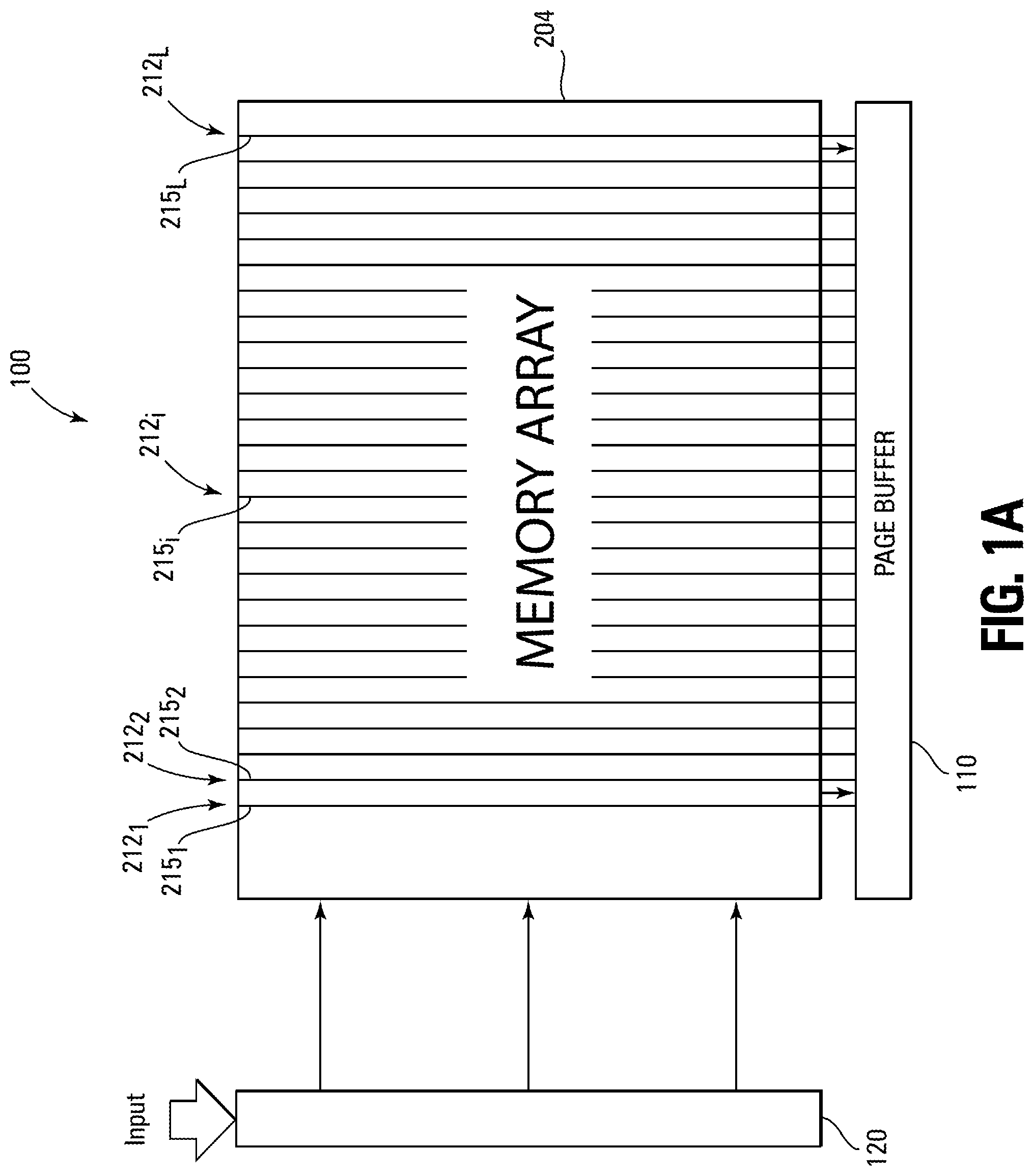
FIG. 1A is a block diagram of a memory device 100, e.g., a NAND, NOR, CAM memory device, etc. Memory device 100 may include a memory array 204. Memory array 204 may be organized into columns 212 of memory cells, such as columns 212.sub.1 to 212.sub.L, that may be respectively accessed by data lines (e.g., bit lines 215.sub.1 to 215.sub.L). A page buffer 110 may be coupled to bit lines 215. An input buffer 120 may also be coupled to memory array 204. The input buffer 120 can be used to temporarily store input data (e.g., an input feature vector), such as key data, for comparison (e.g., during a read operation performed on array 104) to data stored in memory array 104. Data stored in each column 212 of memory array 204 can be referred to as a data feature vector.
For example, the data feature vectors stored in columns 212 of memory array 104 may correspond to known entities, such as known patterns, and memory device 100 may be configured to determine whether an input feature vector at least partially matches a particular known entity represented by a data feature vector, thereby at least potentially identifying the input feature vector as being the particular known entity.
Memory device 100 may be configured to identify the input feature vector as being a particular known entity in response to determining that the input feature vector potentially matches the data feature vector representing the particular known entity. For example, memory device 100 may be configured to identify the data feature vectors most likely to match the input feature vector based on how closely the data feature vectors match the input feature vector.
Components of the input feature vector correspond to certain features (e.g., attributes) of the input feature vector, and thus the entity represented by the input feature vector. Similarly, components of the data feature vectors correspond to certain features (e.g., attributes) of the data feature vectors, and thus the entities represented by the data feature vectors. For example, each data feature vector and the input feature vector may be a pattern, such as of a person's face, fingerprint, etc., and the components may be the features of that pattern.
Components of the input feature vector may be compared to like components of the data feature vectors to determine which data feature vectors potentially match the input feature vector, thereby identifying the entity represented by the input feature vector. For some embodiments, an input feature vector may be determined to potentially match a data feature vector even though there might be a mismatch of certain components.
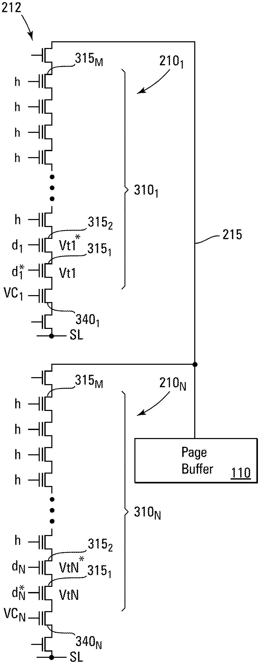
FIG. 1B illustrates an example of a column 212 of memory array 204, e.g., configured according to the NAND architecture. Column 212 comprises N strings (e.g., NAND strings) 310.sub.1 to 310.sub.N of series-coupled memory cells 315. One end of each of strings 310.sub.1 to 310.sub.N is coupled to the same bit line 215 that is coupled in turn to page buffer 110. The opposite end of each of strings 310.sub.1 to 310.sub.N is coupled to a source line SL. The bit line 215 acts as a summing node for the outputs from of each of strings 310.sub.1 to 310.sub.N. For some embodiments, strings 310.sub.1 to 310.sub.N may be respectively blocks 210.sub.1 to 210.sub.N of memory cells 315.
The h signals in FIG. 1B can be a pass signals. In an embodiment, the pass signal h has a voltage level high enough (e.g., about 4V in a particular embodiment) to operate a memory cell having its control gate coupled thereto as a pass-transistor, regardless of the programmed Vt of the memory cell. According to an embodiment, pass signals h might be applied to control gates of unselected memory cells of a string of memory cells (e.g., those memory cells corresponding to the at least a portion of a value of a feature not then being compared) to operate them as pass-transistors.
Memory cells 315.sub.1 and 315.sub.2 may be viewed as switches that selectively allow current to flow from a respective string 310 to bit line 215, or vice versa, when the remaining memory cells in the respective string are operating as pass-transistors. A mismatch between a component of a data feature vector stored in a string 310 and a like component of an input feature vector results in current flow in that string 310.
Resistors 340.sub.1 and 340.sub.N are respectively coupled in series with strings 310.sub.1 and 310.sub.N and respectively control the analog value of current through strings 310.sub.1 and 310.sub.N. For example, resistors 340.sub.1 and 340.sub.N may act as constant current sources of varying values.
The current value through a string can be set by setting the resistance of the respective resistor 340. For example, the resistance of a resistor 340 can be set by programming the threshold voltage of the resistor 340, setting the channel length of the resistor 340 to a specific value, setting the voltage VC applied to the control gate of the resistor 340 to a specific value, etc. Multiple resistors 340 may be in series for additional control (compensation) if appropriate.
The ratio of current may be binary. For example, for a unit of current through string 310.sub.1, the currents through strings 310.sub.2 to 310.sub.N might respectively be 1/2 to 1/2.sup.N-1 of a unit, where N is the block (e.g. string number), e.g., starting at 1. The string corresponding to the most significant bit, e.g., string 310.sub.1, may have a weight of 1 and a unit current in the event of a mismatch, and the string corresponding to the least significant bit, e.g., string 310.sub.N, may have the smallest weight, e.g., 1/2.sup.N-1, and a current of 1/2.sup.N-1 of a unit in the event of a mismatch.
In an example, a feature A1=(a.sub.1, a.sub.2, a.sub.3, a.sub.4, . . . , a.sub.N) of a data feature vector may be programmed as 1011, e.g., for N=4. A feature B1=(b.sub.1, b.sub.2, b.sub.3, b.sub.4, . . . , b.sub.N) of an input feature vector may be input as 1010, e.g., for N=4, for comparison to feature A1. Since a mismatch occurs in the fourth significant bit, corresponding to the least significant bit in this case, the value of the current flow will be 1/2.sup.4-1)=1/8 of a unit. This may be referred to as the least significant bit value of current. Note that bits a.sub.1 through a.sub.N may be respectively stored in blocks 210.sub.1 through 210.sub.N (e.g., strings 310.sub.1 through 310.sub.N) for some embodiments.
A feature B1=(b.sub.1, b.sub.2, b.sub.3, b.sub.4, b.sub.N) of an input feature vector may input as 0011 for comparison to feature A1. Since a mismatch occurs in the first significant bit, corresponding to the most significant bit in this case, the value of the current flow will be the most significant bit value of current 1/2.sup.1-1)=1 unit.
For some embodiments, the input feature vector can be made up of multiple features (e.g., components of the input feature vector), e.g., IF(B)=(B1, B2, B3, . . . , BN) and each data feature vector can be made up of multiple features (e.g., components of the data feature vectors), e.g., DF(A)=(A1, A2, A3, . . . , AN)
The page buffer 110 may measure the analog current flow in bit line 215. For example, zero current is due to an exact match, and the smallest amount of current is due to a single feature mismatch, e.g., a least significant bit mismatch. A current of weight one results from a most significant bit mismatch. All mismatches in a column may be summed in an analog fashion. The threshold value of what current constitutes a match can be programmable.
In FIG. 1B, the bit values corresponding voltage signals applied to the control gates of memory cells 315.sub.1 and 315.sub.2 are respectively represented by d* and d, where d* is the complement of d and represents not d (e.g., see input data in the state definitions in FIG. 1C). In fact, a superscript * is used herein to denote a complement.
For example, if a corresponding digit of data of a received input feature vector has a binary bit value of b=0, a voltage of about 2V, corresponding to a bit value of d.sub.1=0, may be applied to the control gate of memory cell 315.sub.2 of string 310.sub.1, and a voltage of about 4V, corresponding to a bit value of d.sub.1*=1, may be applied to the control gate of memory cell 315.sub.1 of string 310.sub.1. That is, d.sub.1*=1 and d.sub.1=0 may correspond to a binary bit value of b=0 of a digit of data of the input feature vector, as shown in FIG. 1C. If a corresponding digit of data of a received input feature vector has a binary bit value of b=1, a voltage of about 4V, corresponding to a bit value of d.sub.1=1, may be applied to the control gate of memory cell 315.sub.2 of string 310.sub.1, and a voltage of about 2V, corresponding to a bit value of d.sub.1*=0, may be applied to the control gate of memory cell 315.sub.1 of string 310.sub.1. That is, d.sub.1*=0 and d.sub.1=1 may correspond to a binary value of b=1 of a digit of data of the input feature vector, as shown in FIG. 1C.
Memory cells 315.sub.1 and 315.sub.2 of string 310.sub.1 might be respectively programmed to threshold voltages Vt1 and Vt1* to store at least a portion of a value of a feature of the data feature vector stored in string 310.sub.1. For example, memory cells 315.sub.1 and 315.sub.2 of string 310.sub.1 might be respectively programmed to threshold voltages Vt1 and Vt1* of about 1V and about 3V to store a binary value of a=0 for a digit of data of the stored data feature vector. For example, when memory cell 315.sub.1 is programmed to a threshold voltage Vt1 of about 1V, memory cell 315.sub.1 may store a bit value of z=0, and when memory cell 315.sub.2 is programmed to a threshold voltage Vt1* of about 3V, memory cell 315.sub.2 may store a bit value of z*=1. This means that when memory cells 315.sub.1 and 315.sub.2 respectively store bit values of z=0 and z*=1, memory-cell pair 315.sub.1, 315.sub.2 stores a binary value of a=0, as shown in FIG. 1C.
Memory cells 315.sub.1 and 315.sub.2 of string 310.sub.1 might be respectively programmed to threshold voltages Vt1 and Vt1* of about 3V and about 1V to store a binary value of a=1 for the digit of data of the data feature vector. For example, when memory cell 315.sub.1 is programmed to a threshold voltage Vt1 of about 3V, memory cell 315.sub.1 may store a bit value of z=1, and when memory cell 315.sub.2 is programmed to a threshold voltage Vt1* of about 1V, memory cell 315.sub.2 may store a bit value of z*=0. This means that when memory cells 315.sub.1 and 315.sub.2 respectively store bit values of z=1 and z*=0, memory-cell pair 315.sub.1, 315.sub.2 stores a binary value of a=1, as shown in FIG. 1C. Similarly, memory cells 315.sub.1 and 315.sub.2 of string 310.sub.N might be respectively programmed to threshold voltages VtN and VtN* to store at least a portion of a value of a feature of the data feature vector stored in string 310.sub.N.
The logic truth table of FIG. 1C illustrates the results from comparing a digit b of input data, such as of a feature (e.g., component) B of an input feature vector, to a digit a of corresponding stored data, such as of a same feature (e.g., component) A of a stored data feature vector. With additional reference to FIG. 1B, for example, during a compare operation of an input data to stored data, for a digit a, signals, corresponding to the bit values d* and d, are respectively applied to the control gates of the memory cells 315.sub.1 and 315.sub.2 of string 310.sub.1.
If the voltage of the signal corresponding to the respective d*/d bit value is greater than the programmed threshold voltage (e.g., Vt* or Vt) of the respective memory cell (e.g., 315.sub.1 and 315.sub.2), the respective memory cell will conduct, e.g., and will be ON. If the voltage of the signal corresponding to the respective d*/d bit value is less than the programmed threshold voltage (e.g., Vt* or Vt) of the respective memory cell (e.g., 315.sub.1 and 315.sub.2), the respective memory cell will not conduct, e.g., and will be OFF. According to an embodiment implementing the truth table of FIG. 1C, if the value of digit b matches the value of digit a, at least one of the memory cells (e.g., 315.sub.1 and 315.sub.2) will not conduct, e.g., and will be OFF, in response to receiving the signals corresponding to the bit values d* and d selected in accordance with the value of digit b.
Referring to FIG. 1C, the first column includes three possible values (binary 0, binary 1, and X) for digit b. For a particular digit b, for example, signals corresponding to the bit values d* and d, selected in accordance with the value of digit b, can be applied to the control gates of a corresponding pair of memory cells (e.g., memory cells 315.sub.1 and 315.sub.2 of string 310.sub.1). For example, if the digit b has a value of binary 0, a signal having a voltage level of about 4V, e.g., corresponding to a bit value d.sub.1*=1, might be applied to the control gate of a first memory cell (e.g., memory cell 315.sub.1) of the pair, and a signal having a voltage level of about 2V, e.g., corresponding to a bit value d.sub.1=0, might be applied to the control gate of a second memory cell of the pair (e.g., memory cell 315.sub.2).
Continuing with such an example, if the digit b has a value of binary 1, a signal having a voltage level of about 2V, e.g., corresponding to a bit value d.sub.1*=0, might be applied to the control gate of the first memory cell (e.g., memory cell 315.sub.1) of the pair, and a signal having a voltage level of about 4V, e.g., corresponding to a bit value d.sub.1=1, might be applied to the control gate of a second memory cell of the pair (e.g., memory cell 315.sub.2).
Further continuing with the example, if do not care data X has been inserted into the digit d, a signal having a voltage level of about 0V might be applied to the control gate of the first memory cell (e.g., memory cell 315.sub.1) of the pair, and a signal having a voltage level of about 0V might also be applied to the control gate of the second memory cell of the pair (e.g., memory cell memory cell 315.sub.2), thus ensuring neither cell of the pair conducts, assuring a match no matter what actual data is stored by the pair of cells.
The F entry in the first column of FIG. 1C corresponds to an operation corresponding to memory cells in a pass-through mode, such as where their control gates are both biased with the pass through signal h (e.g., allowing other digits to be compared).
Each row of the second column of FIG. 1C illustrates four possible values for digit a (i.e., the digit of data being compared to the digit b). For a particular digit a, for example, a pair of memory cells can be programmed to threshold voltages (e.g., Vt1, Vt1*, corresponding to stored bit values z and z*) selected in accordance with the value of digit a.
For example, if the digit a has a value of binary 0, a first memory cell (e.g., memory cell 315.sub.1 of string 310.sub.1) of the pair might be programmed to a threshold voltage (e.g., Vt1) of about 1V, while the second memory cell of the pair (e.g., memory cell 315.sub.2 of string 310.sub.1) might be programmed to a threshold voltage (e.g., Vt1*) of about 3V. Continuing with such an example, if the digit a has a value of binary 1, a first memory cell (e.g., memory cell 315.sub.1 of string 310.sub.1) of the pair might be programmed to a threshold voltage (e.g., Vt1) of about 3V, while the second memory cell of the pair (e.g., memory cell 315.sub.2 of string 310.sub.1) might be programmed to a threshold voltage (e.g., Vt1*) of about 1V.
Further continuing with the example, to store do not care data X for digit a, a first memory cell (e.g., memory cell 315.sub.1 of string 310.sub.1) of the pair might be programmed to a threshold voltage (e.g., Vt1) of about 3V, and the second memory cell of the pair (e.g., memory cell 315.sub.2 of string 310.sub.1) might also be programmed to a threshold voltage (e.g., Vt1*) of about 3V, thus ensuring that at least one cell of the pair does not conduct regardless of the selected the voltage of the signal corresponding to the respective d*/d bit value, and thereby assuring a match regardless of the value of digit b. Still further, in a another variation, the memory cells have not been programmed to store either a binary 0, a binary 1, or do not care data X (e.g., they both have a threshold voltage of about 1V), in which case a match with digit b is only detected if do not care data has been inserted into digit b.
Each row of the third column of FIG. 1C illustrates a respective result of comparing the value of digit b to each of the four possible values for digit a. A binary 1 indicates no current conduction on the bit line coupled to the string. A binary 0 indicates that current is flowing. Thus, referring to the first row of the third column of FIG. 1C, when digit b has a value of binary 0 and the corresponding pair of memory cells store a binary 1, the result is binary 0--indicating a no match condition. When the digit b has a value of binary 0 and the corresponding pair of memory cells store a binary 0, the result is binary 1--indicating a match condition. When the digit b has a value of binary 0 and the corresponding pair of memory cells store do-not-care data X, the result is binary 1--indicating a match condition. When the digit b has a value of binary 0 and the pair of memory cells is erased F, the result is 0--indicating a no match condition.
FIG. 1C also includes examples of state definitions from the logic truth table. The input the bit values d and d*, selected in accordance with the value of digit b, have the illustrated logic highs H (logic 1) and logic lows L (logic 0) as indicated. The memory array stores z and z*, selected in accordance with the value of digit a, having the illustrated logic highs H and logic lows L as indicated.
FIG. 2 is a block diagram that illustrates a portion of memory device 100 that includes memory array 204, page buffer 110, and input buffer 120. For some embodiments, memory array 204 may be organized in blocks 210 of memory cells, such as blocks 210.sub.1 to 210.sub.N.
Each column 212 may include memory cells from each of blocks 210. Each block 210 may include access lines (e.g., word lines 220) respectively coupled to rows of memory cells in each block 210 so that each block 210 is organized in rows and columns of memory cells.
Bit lines 215.sub.1 to 215.sub.L may be respectively coupled, one-to-one, to current sense amplifiers, such as sense amps 225.sub.1 to 225.sub.L that may have analog-to-digital converter functionality. Sense amps 225.sub.1 to 225.sub.L may be respectively coupled, one-to-one, to comparators 228.sub.1 to 228.sub.L. A single register 230 (e.g., that may be referred to as difference register), in some embodiments, may be coupled to comparators 228.sub.1 to 228.sub.L. Sense amps 225, comparators 228, and register 230 may be part of page buffer 110 for some embodiments. For other embodiments, there may be a plurality of individual difference registers, where the individual difference registers are coupled one-to-one to comparators 228.sub.1 to 228.sub.L.
Word lines 220 may be coupled to respective ones of drivers 232 for receiving voltages therefrom. Mask registers 240 may be coupled to drivers 232, and may be used to mask certain blocks 210 or certain cells of blocks 210 when reading from or writing to array 204. For example, mask registers 240 may be coupled one-to-one to word lines 220. Drivers 232 and mask register 240 may be part of input buffer 120 for some embodiments. In other words, mask registers 240 may mask memory cells coupled thereto. For example, a mask register 240 may store a mask bit that causes a memory cell coupled thereto to be masked.
Input (e.g., key) registers 245 (e.g., which may also be referred to as input feature registers) may be coupled one-to-one to mask registers 240, and thus to word lines 220, and may be part of input buffer 120 for some embodiments. For other embodiments, the input feature registers 245 and mask registers 240 may be interchanged so that input feature registers 245 are between mask registers 240 and drivers 232.
Note that the set of input feature registers receive input data, such as input feature vectors, for comparison to data, such as data feature vectors, stored in columns 212 of memory array 204. For example, an input feature vector may be programmed into resisters 245.
Each component of a data feature vector may be stored in one or more blocks 210. For some embodiments, multiple components of a data feature vector may be stored in a single block. For other embodiments, components for multiple data feature vectors may be stored in a single block.
Each feature (e.g., component) of a feature vector may be expressed by a binary expression of data having a most significant bit, a least significant bit, and bits of differing significance between the most significant bit and the least significant bit, where bits of the input feature vector are compared to bits of each data feature vector having like significance. For example, the most significant bit of the input feature vector may be compared to the most significant bit of a data feature vector, the least significant bit of the input feature vector to the least significant bit of the data feature vector, etc. The bits of a feature (e.g., component) of a data feature vector may be respectively stored in different blocks 210 of a group of blocks 210; the bits of another feature (e.g., component) of the data feature vector may be respectively stored in different blocks 210 of another group of blocks 210; etc.
For some embodiments, more than one bit of a component of a data feature vector can be stored in a single block. For example, multiple bits for a single component of a data feature vector can be stored in a single block. In addition, bits for multiple components of a data feature vector can be stored in a single block.
For some embodiments, each sense amp 225 may sense a level of a current I.sub.A on a respective one of bit lines 215 and may convert the sensed current level I.sub.A to a digital representation I.sub.D (e.g., a voltage level representing a sensed current level) of the level of the sensed current I.sub.A. Each sense amp 225 may send the representation I.sub.D to a respective comparator 228.
Register 230 may store a particular reference I.sub.ref (e.g., a voltage level) to be compared to the representation I.sub.D at the respective comparator 228. That is, the respective comparator 228 may receive the particular reference I.sub.ref from register 230 and compare the particular reference I.sub.ref to the representation I.sub.D. For example, comparator 228.sub.1 may receive the particular reference I.sub.ref from register 230 and compare the particular reference I.sub.ref to representation I.sub.D1 that is a digital representation of the level of the sensed current I.sub.A1 on bit line 215.sub.1; comparator 228.sub.2 may receive the particular reference I.sub.ref from register 230 and compare the particular reference I.sub.ref to representation I.sub.D2 that is a digital representation of the level of the sensed current I.sub.A2 on bit line 215.sub.2; and so on, until comparator 228.sub.L receives the particular reference I.sub.ref from register 230 and compares the particular reference I.sub.ref to representation I.sub.DL that is a digital representation of the level of the sensed current I.sub.AL on bit line 215.sub.L.
For some embodiments, a representation I.sub.D that is less than or equal to the particular reference I.sub.ref may be indicative of a potential match, between data (e.g., a data feature vector) stored in a respective column 212 and input data (e.g., an input feature vector) stored in registers 245, and a representation I.sub.D that is greater than the particular reference I.sub.ref may be indicative of no match between the data stored in the respective column 212 and the data stored in registers 245. For example, memory device 100 may be configured to determine that there is a potential match in response to the representation I.sub.D being less than or equal to the particular reference I.sub.ref and no match in response to the representation I.sub.D being greater than the particular reference I.sub.ref. For example, if the representation I.sub.D1 is less than or equal to the particular reference I.sub.ref, the input feature vector is potentially an exact match to the data feature vector stored in column 212.sub.1, and if the number I.sub.D2 is less than or equal to the particular reference I.sub.ref, the input feature vector is potentially an exact match to the data feature vector stored in column 212.sub.2, whereas if the representation I.sub.DL is greater than the particular reference I.sub.ref, the input feature vector is not a potential match to the data feature vector stored in column 212.sub.L.
For other embodiments, to vary the number of potential matches and/or to identify data feature vectors that may have a greater or lesser potential of matching the input feature vector, register 230 may be programmable so that a user, for example, can program different particular references I.sub.ref into register 230. For example, larger particular references I.sub.ref, can potentially identify a larger number of data feature vectors that potentially match the input feature vector than smaller particular references I.sub.ref, in that the larger particular reference I.sub.ref allows for data feature vectors that are further away from matching the input feature vector than the smaller particular references I.sub.ref. For example, larger particular references I.sub.ref may be used when a smaller reference I.sub.ref yields little or no data feature vectors potentially matching the input feature vector. Conversely, if there are too many data feature vectors potentially matching the input feature vector, the particular reference I.sub.ref may be reduced, in that the smaller particular reference I.sub.ref requires data feature vectors potentially matching the input feature vector to be closer to the input feature vector than a larger value of the particular reference I.sub.ref.
For some embodiments, progressively reducing the particular reference I.sub.ref can act to identify the data feature vectors that are closest to the input feature vector. For other embodiments, setting the particular reference I.sub.ref to zero identifies data feature vectors that are an exact match to the input feature vector.
The level of a current I.sub.A on a respective one of bit lines 215 might not be zero, in that there may be some current leakage through a memory cell that is turned off, and thus though the string containing that memory cell and the bit line 215 coupled to that string. Therefore, the digital representation I.sub.D that is compared to I.sub.ref might not be zero. Therefore, to compensate for such leakage, I.sub.ref may be set to a certain value, e.g., corresponding to a predetermined current leakage that may occur, for some embodiments. Then, for some embodiments, if digital representation ID is less than or equal to the certain value, digital representation I.sub.D is taken to be zero. As such, register 230 is configured to store a value of I.sub.ref that compensates for current leakage.
FIG. 3 is a schematic of array 204, e.g., a NAND array. Each bit line 215 may be coupled to a plurality strings 310 (e.g., strings 310.sub.1 to 310.sub.N respectively of blocks 210.sub.1 to 210.sub.N) of memory cells 315.sub.1 to 315.sub.M. The memory cells 315 may represent non-volatile memory cells for storage of data. The memory cells 315 of each string 310 are connected in series, source to drain, between a source select gate 320 and a drain select gate 322. Therefore, a column 212 of memory cells 315 may include a plurality of strings 310 coupled to a given bit line 215. Each drain select gate 322 selectively couples an end of a corresponding string 310 to a corresponding bit line 215. Drain select gates 322 may be commonly coupled to a drain select line 321, and source select gates 320 may be commonly coupled to a source select line 323.
Typical construction of a memory cell 315 may include a source 325, a drain 328, a charge-storage structure 330 (e.g., a floating gate, charge trap, etc.) that can store a charge that determines a data value of the cell, and a control gate 332, as shown in FIG. 3. Memory cells 315 have their control gates 332 respectively coupled to (and in some cases form) word lines 220. For example, in each of blocks 210.sub.1 to 210.sub.N, memory cells 315.sub.1 to 315.sub.M may have their control gates 332 respectively coupled to (and in some cases from) word lines 220.sub.1 to 220.sub.M. A row of the memory cells 315 may be those memory cells commonly coupled to a given word line 220.
A resistor (e.g., one or more resistors) 340 may be coupled in series with each string 310 of memory cells 315. For example, one or more resistors 340 may be between and coupled in series with a source select gate 320 and a memory cell 315.sub.1 located at an end of a respective string 310 that is opposite the end coupled to a drain select gate 322. Each source select gate 320 may selectively couple a resistor 340, and thus a respective string 310, to a source line (not shown). Although two series-coupled resistors 340 are shown in FIG. 3, one resistor 340 may be coupled in series with each string 310, or more than two series-coupled resistors 340 may be coupled in series with each string 310 for more control over the resistance. For example, the more resistors 340 coupled in series with a string 310, the more control over the resistance on that string.
For embodiments where more than one resistor 340 is coupled to a string 310, the resistances of the respective resistors may be same as each other or different than each other. In the example of FIG. 3, each string 310.sub.1 in block 210.sub.1 may be coupled to resistors 340.sub.1,1 and 340.sub.2,1; each string 310.sub.2 in block 210.sub.2 may be coupled to resistors 340.sub.1,2 and 340.sub.2,2; and . . . each string 310.sub.N in block 210.sub.N may be coupled to resistors 340.sub.1,N and 340.sub.2,N.
The overall resistance of the one or more resistors 340 coupled to each string 310.sub.1 in block 210.sub.1 may be different than the overall resistance of the one or more resistors 340 coupled to each string 310.sub.2 in block 210.sub.2, and the overall resistance of the one or more resistors 340 coupled to each string 310.sub.2 in block 210.sub.2 may be different than the overall resistance of the one or more resistors 340 coupled to each string 310.sub.N in block 210.sub.N. For example, for some embodiments, the overall resistance of the one or more resistors 340 coupled to each string in each block 210 may be different than the overall resistance of the one or more resistors 340 coupled to each string 310 in every other block 210.
The one or more resistors 340 respectively coupled in series with strings 310.sub.1, 310.sub.2, and . . . 310.sub.N respectively cause different levels of current to flow through strings 310.sub.1, 310.sub.2, and . . . 310.sub.N, e.g., when strings 310.sub.1, 310.sub.2, and . . . 310.sub.N are discharged from a common voltage level to ground. For example, the strings may be discharged through an activated source select gate 320 to a source line that may be coupled to ground.
The one or more resistors 340 coupled to each string 310 act to weight the respective string 310. Accordingly, differently weighted strings 310.sub.1 to 310.sub.N make different contributions to the overall level of the current flowing through a precharged bit line 215 coupled to and discharging through the differently weighted strings 310.sub.1 to 310.sub.N. This allows the bits of data respectively stored in the memory cells 315 of strings 310.sub.1 to 310.sub.N to be weighted differently. For example, the bits of data respectively stored in the memory cells 315 of strings 310.sub.1 to 310.sub.N can be weighted according to their significance.
For example, for some embodiments, strings 310.sub.1 to 310.sub.N may be respectively coupled to increasing resistances, and the memory cells of strings 310.sub.1 to 310.sub.N may respectively store most significant bits to least significant bits. In other words, the lower the resistance coupled to a given string, the higher the potential current flow through that string and the higher the significance of the bits of data stored in the memory cells of that string. For some embodiments, each string 310.sub.1 may be coupled to the lowest resistance and may store the most significant bits of data, and each string 310.sub.N may be coupled to the highest resistance and may store the least significant bits of data.
For some embodiments, each resistor 340 may be a transistor configured to act as a resistor. For example, the resistance of a transistor may be related to the channel length of the transistor, where the greater the channel length the greater the resistance. Therefore, the resistances on each string may be preset, e.g., during fabrication of the memory array, by fabricating the transistor, acting as a resistor, to have a predetermined channel length.
For example, strings 310.sub.1 to 310.sub.N may be respectively coupled to increasing resistances by fabricating the transistors, acting as resistors, respectively coupled in series with strings 310.sub.1 to 310.sub.N to respectively have increasing channel lengths. For embodiments, where resistors with different resistances are coupled to a particular string, the different resistances may be respectively preset by respectively coupling transistors with different channel lengths to the particular string.
For other embodiments, each resistor 340 may be a programmable resistor. For example, each resistor 340 may be configured in a manner similar to a memory cell 315. In one example, each resistor 340 may be a charge-storage cell having a charge storage structure 342 and a control gate 344 coupled to (and in some cases forming) a control line 345. For example, the control gates of resistors 340.sub.1,1, 340.sub.2,1, 340.sub.1,2, 340.sub.2,2, 340.sub.1,N, and 340.sub.2,N may be respectively coupled to control lines 345.sub.1,1, 345.sub.2,1, 345.sub.1,2, 345.sub.2,2, 345.sub.1,N, and 345.sub.2,N.
The resistance of a charge-storage cell is related to a difference between the threshold voltage programmed into the charge-storage cell and a voltage VC applied to the control gate 344 (e.g., the voltage placed on a corresponding control line 345). For example, a small difference, e.g., corresponding to charge-storage cell being partially ON, may produce a large resistance, and progressively increasing the difference, may progressively decrease the resistance until the difference is large enough that the charge-storage cell is fully ON, e.g., is placed in a read mode. For other embodiments, the each resistor 340 may be programed to the same threshold voltage, and the voltages VC applied to the control gates may be adjusted to adjust the resistance. Control lines 345 may be coupled to drivers, such as drivers 232, that apply the voltages VC.
For some embodiments, the voltage VC that is to be applied to the control gate of a resistor 340 to effect a certain reduction in the current level may be determined from an iterative process. For example, the resistor is programmed to a certain threshold voltage and the voltage VC is adjusted until the desired current level is obtained. The voltage VC thus obtained may be subsequently used in conjunction with the threshold voltage to cause the resistor 340 to set the current flow through a corresponding string 310.
In one example, the voltages VC.sub.1,1 and VC.sub.2,1 respectively applied to control lines 345.sub.1,1 and 345.sub.2,1 and the threshold voltages of the resistors 340.sub.1,1 and 340.sub.2,1 respectively coupled to control lines 345.sub.1,1 and 345.sub.2,1 may cause the voltages VC.sub.1,1 and VC.sub.2,1 to act as pass voltages so that resistors 340.sub.1,1 and 340.sub.2,1 provide little resistance to any current flowing through the respective string 310.sub.1. As such, the resistors 340.sub.1,1 and 340.sub.2,1 may be set to reduce the current level by substantially a factor of one, e.g., substantially no reduction, and thus the strings 310.sub.1 coupled in series with resistors 340.sub.1,1 and 340.sub.2,1 may be said to have a weight factor of substantially one. For some embodiments, the strings 310.sub.1 in columns 212 may store the most significant bits of data (e.g., data feature vectors) stored in those columns.
Continuing with the example, the voltages VC.sub.1,2 and VC.sub.2,2 respectively applied to control lines 345.sub.1,2 and 345.sub.2,2 and the threshold voltages of the resistors 340.sub.1,2 and 340.sub.2,2 respectively coupled to control lines 345.sub.1,2 and 345.sub.2,2 may cause the overall (e.g., combined) resistance of the resistors 340.sub.1,2 and 340.sub.2,2 to be, for example, substantially two times the combined resistance of resistors 340.sub.1,1 and 340.sub.2,1. As such, resistors 340.sub.1,2 and 340.sub.2,2 may act to reduce the current level by substantially a factor of 2, and thus the strings 310.sub.2 coupled in series with resistors 340.sub.1,2 and 340.sub.2,2 may be said to have a weight factor of substantially 1/2. That is, the current flow through resistors 340.sub.1,2 and 340.sub.2,2 may be substantially a factor of two less than through resistors 340.sub.1,1 and 340.sub.2,1. For some embodiments, the strings 310.sub.2 in columns 212 may store the next-most (e.g., the second-most) significant bits of data (e.g., data feature vectors) stored in those columns.
Continuing further with the example, the voltages VC.sub.1,N and VC.sub.2,N respectively applied to control lines 345.sub.1,N and 345.sub.2,N and the threshold voltages of the resistors 340.sub.1,N and 340.sub.2,N respectively coupled to control lines 345.sub.1,N and 345.sub.2,N may cause the combined resistance of the resistors 340.sub.1,N and 340.sub.2,N coupled thereto to be, for example, substantially 2.sup.N-1 times the combined resistance of resistors 340.sub.1,1 and 340.sub.2,1. As such, resistors 340.sub.1,N and 340.sub.2,N may act to reduce the current level by substantially a factor of 2.sup.N-1, and thus the strings 310.sub.N coupled in series with resistors 340.sub.1,N and 340.sub.2,N may be said to have a weight factor of substantially 1/2.sup.N-1. That is, the current flow through resistors 340.sub.1,N and 340.sub.2,N may be substantially a factor of 2.sup.N-1 less than through resistors 340.sub.1,1 and 340.sub.2,1. For some embodiments, the strings 310.sub.N in columns 212 may store the least significant bits of data (e.g., data feature vectors) stored in those columns.
For some embodiments, bits of data of a data feature vector to be compared to like bits of data of an input feature vector may be stored in pairs of memory cells 315 so that each string 310 may store M/2 bits of data. For example, a memory-cell pair 315.sub.1, 315.sub.2 of string 310.sub.1 may store the most significant bit of a component of a data feature vector to be compared to the most significant bit of the same component of the input feature vector; a memory-cell pair 315.sub.1, 315.sub.2 of string 310.sub.N may store the least significant bit of the component of the data feature vector to be compared to the least significant bit of the component of the input feature vector; and the memory-cell pair 315.sub.1, 315.sub.2, of string 310.sub.2 may store a bit (e.g., the second-most significant bit) of the component of the data feature vector between the most significant bit and the least significant bit of the component of the data feature vector to be compared to a like bit (e.g., the second-most significant bit) of the component of the input feature vector between the most significant bit and the least significant bit of the component of the input feature vector.
Another memory-cell pair of string 310.sub.1 may store the most significant bit of another component of the data feature vector stored in the respective column 212 to be compared to the most significant bit of another component of the input feature vector; another memory-cell pair of string 310.sub.2 may store the second-most significant bit of the other component of the data feature vector stored in the respective column 212 to be compared to the second-most significant bit of the other component of the input feature vector; and another memory-cell pair of string 310.sub.N may store the least significant bit of the other component of the data feature vector stored in the respective column 212 to be compared to the least significant bit of the other component of the input feature vector. Each bit of a input feature vector may correspond to the values (e.g., bit values d and d*) stored in two registers 245 (FIG. 2).
In the example of FIG. 4, an input feature vector 400 (e.g., IF(B)=(B1, B2, BN) is programmed into registers of memory device 100, such as input registers 245 of input buffer 120. Input feature vector 400 may have components B1, B2, and BN. For example, the input feature vector 400 may represent a pattern, and each component B may be a feature (e.g., attribute) of the pattern. For example, each component B may be a feature of an unknown person. To simplify the example of FIG. 4, each component B may correspond to a single binary bit that may have a value of binary 1 or binary 0. For example, the value of components B1, B2, and BN may be respectively, binary 0, (corresponding bit values d.sub.1*=1 and d.sub.1=0), binary 1 (corresponding bit values d.sub.2*=0 and d.sub.2=1), and binary 1 (corresponding bit values d.sub.N*=0 and d.sub.N=1), as shown in FIG. 4. However, for other embodiments, each feature B may have a value expressed by a plurality of binary bits.
Component B1 may be the most important feature in a comparison of input feature vector 400 to data feature vectors stored in memory array 204, component B2 the next-most (e.g., the second-most) important feature of input feature vector 400, and component BN the least important feature of input feature vector 400. Therefore, the bit of component B1 may be the most significant bit of a binary expression of input feature vector 400; the bit of component B2 may be the second-most significant bit of the binary expression of input feature vector 400; and the bit of component BN may be the least significant bit of the binary expression of input feature vector 400. As such, input feature vector 400 may be represented by the binary expression 011, e.g., IF(B)=011.
Note that each component (e.g., bit in this example) of input feature vector 400 may use two register bits d and d*. For example, a register bit 0 may cause a voltage V.sub.WL=2V to be applied to the word line 220 corresponding to the register containing bit 0, and a register bit 1 may cause a voltage V.sub.WL=4V to be applied to the word line 220 corresponding to the register containing bit 1.
For some embodiments, a 0 value (bit) of input feature vector 400 may be coded as a first voltage (e.g., 2V) in a first register bit and a second voltage (e.g., 4V) in a second register bit in a pair of registers 245, and a 1 value (bit) of input feature vector 400 may be coded as the second voltage (e.g., 4V) in a first register bit and the first voltage (e.g., 2V) in the second register bit in a pair of registers 245, as shown in FIG. 4.
In the example of FIG. 4, input feature vector 400 is to be compared to a data feature vector stored in each of columns 212.sub.1, 212.sub.2, and 212.sub.L of array 204 of FIG. 3. For example, each data feature vector may be a pattern that is to be compared to the pattern of input feature vector 400. For example, each data feature vector may represent a known person having different attributes respectively stored in blocks 210.sub.1 to 210.sub.N.
For example, a data feature vector DF.sub.1(A)=(A1, A2, AN).sub.1 may be stored in column 212.sub.1; a data feature vector DF.sub.2(A)=(A1, A2, AN).sub.2 may be stored in column 212.sub.2; and a data feature vector DF.sub.L(A)=(A1, A2, AN).sub.L may be stored in column 212.sub.L. Data feature vector DF.sub.1(A) may be equal to the binary expression 000; data feature vector DF.sub.2(A) may be equal to the binary expression 011; and data feature vector DF.sub.N(A) may be equal to the binary expression 111. Therefore, there is an exact match between input feature vector 400 (e.g., input feature vector IF(B)=011) and data feature vector DF.sub.2(A), a mismatch between the most significant bits of input feature vector IF(B) and data feature vector DF.sub.N(A), and a mismatch between the second-most significant bits of input feature vector IF(B) and data feature vector DF.sub.1(A) and the least significant bits of input feature vector IF(B) and data feature vector DF.sub.1(A). As discussed below, the most, second-most, and least significant bits may respectively have the weight factors of 1, 1/2, and 1/2.sup.N-1
For some embodiments, a plurality of bits may be stored in a string of memory cells. For example, each of a plurality of memory-cell pairs in a string may store a bit. The bits stored in a string of memory cells may be bits of different components of a data feature vector. Alternatively, the bits stored in a string of memory cells may be different bits of a single component of a data feature vector.
The data stored in columns 212.sub.1, 212.sub.2, and 212.sub.L in block 210.sub.1 may represent a component (e.g., a feature) A1 of the data feature vectors stored in columns 212.sub.1, 212.sub.2, and 212.sub.L and may be in the same category (e.g., of the same type) as component B1 of input feature vector 400; the data stored in columns 212.sub.1, 212.sub.2, and 212.sub.L in block 210.sub.2 may represent a component (e.g., a feature) A2 of the data feature vectors stored in columns 212.sub.1, 212.sub.2, and 212.sub.L and may be in the same category (e.g., of the same type) as component B2 of input feature vector 400; and the data stored in columns 212.sub.1, 212.sub.2, and 212.sub.L in block 210.sub.N may represent a component (e.g., a feature) AN of the data feature vectors stored in columns 212.sub.1, 212.sub.2, and 212.sub.L and may be in the same category (e.g., of the same type) as component BN of input feature vector 400. For example input feature vector 400 and the data feature vectors stored in columns 212.sub.1, 212.sub.2, and 212.sub.L may represent people, and like components A1 and B1 may be race, like components A2 and B2 may be height, and like components AN and BN may be eye color, i.e., race, height, and eye color may be different categories.
Therefore, component B1 of input feature vector 400 (e.g., input feature vector IF(B)) will be compared to component A1 of data feature vectors DF.sub.1(A), DF.sub.2(A), and DF.sub.L(A). Component B2 of the input feature vector IF(B) will be compared to component A2 of data feature vectors DF.sub.1(A), DF.sub.2(A), and DF.sub.L(A). Component BN of the input feature vector IF(B) will be compared to component AN of data feature vectors DF.sub.1(A), DF.sub.2(A), and DF.sub.L(A).
Component A1 of the data feature vector stored in each of columns 212.sub.1, 212.sub.2, and 212.sub.L may be stored in the memory-cell pair 315.sub.1, 315.sub.2 of string 310.sub.1 in each of columns 212.sub.1, 212.sub.2, and 212.sub.L; component A2 of the data feature vector stored in each of columns 212.sub.1, 212.sub.2, and 212.sub.L may be stored in the memory-cell pair 315.sub.1, 315.sub.2 of string 310.sub.2 in each of columns 212.sub.1, 212.sub.2, and 212.sub.L; and component AN of the data feature vector stored in each of columns 212.sub.1, 212.sub.2, and 212.sub.L may be stored in memory-cell pair 315.sub.1, 315.sub.2 of string 310.sub.N in each of columns 212.sub.1, 212.sub.2, and 212.sub.L. Note that strings 310.sub.1, 310.sub.2, and 310.sub.N are respectively in blocks 210.sub.1, 210.sub.2, and 210.sub.N (FIG. 3).
For some embodiments, the components A1, A2, and A3 of the data feature vector stored in each of columns 212.sub.1, 212.sub.2, and 212.sub.L may respectively be the most, second-most, and least important features in the comparison to input data feature vector 400, and thus may respectively be the most, second-most, and least significant bits of the data feature vector stored in each of columns 212.sub.1, 212.sub.2, and 212.sub.L. Component B1 of input data feature vector 400 is to be compared to data stored in the memory-cell pair 315.sub.1, 315.sub.2 of string 310.sub.1 in each of columns 212.sub.1, 212.sub.2, and 212.sub.L. Component B2 of input data feature vector 400 is to be compared to the data stored in the memory-cell pair 315.sub.1, 315.sub.2 of string 310.sub.2 in each of columns 212.sub.1, 212.sub.2, and 212.sub.L. Component AN of input data feature vector 400 is to be compared to the data stored in the memory-cell pair 315.sub.1, 315.sub.2 of string 310.sub.N in each of columns 212.sub.1, 212.sub.2, and 212.sub.L. That is, the most significant bit of the input data (e.g., corresponding to input feature vector 400) is compared to the most significant bit of the data stored in each of columns 212.sub.1, 212.sub.2, and 212.sub.L; the second-most significant bit of the input data is compared to the second-most significant bit of the data stored in each of columns 212.sub.1, 212.sub.2, and 212.sub.L; and the least significant bit of the input data is compared to the least significant bit of the data stored in each of columns 212.sub.1, 212.sub.2, and 212.sub.L.
Each memory cell 315.sub.1 is programed to a threshold voltage Vt, and each memory cell 315.sub.2 is programed to a threshold voltage Vt*. The values of threshold voltages Vt* and Vt are shown in FIG. 4 and represent stored data. For example, memory cells 315.sub.1 and 315.sub.2 in block 210.sub.1 are respectively programed to threshold voltages Vt1 and Vt1*; memory cells 315.sub.1 and 315.sub.2 in block 210.sub.2 are respectively programed to threshold voltages Vt2 and Vt2*; and memory cells 315.sub.1 and 315.sub.2 in block 210.sub.N are respectively programed to threshold voltages VtN and VtN*.
To compare component B1 of input feature vector 400 to the data stored in the memory-cell pair 315.sub.1, 315.sub.2 of string 310.sub.1 in each of columns 212.sub.1, 212.sub.2, and 212.sub.L, the register bits d.sub.1* and d.sub.1 corresponding to component B1 of input feature vector 400 may cause a voltage V.sub.WL1=4V (e.g., corresponding to a bit value of d.sub.1*=1) to be applied to the word line 220.sub.1 (FIG. 3) in block 210.sub.1 and a voltage V.sub.WL2=2V (e.g., corresponding to a bit value of d.sub.1=0) to be applied to the word line 220.sub.2 (FIG. 3) in block 210.sub.1. A pass voltage may be applied to the remaining word lines (e.g., the word lines other than word lines 220.sub.1 and 220.sub.2) in block 210.sub.1. That is, the remaining word lines may receive a voltage that allows the memory cells coupled thereto in the string 310.sub.1 in each of columns 212.sub.1, 212.sub.2, and 212.sub.L to pass current with little resistance.
FIG. 4 shows the status of the memory cell 315.sub.1 in block 210.sub.1 in each of columns 212.sub.1, 212.sub.2, and 212.sub.L in response applying the voltage V.sub.WL1=4V to the word line 220.sub.1 in block 210.sub.1. The status of the memory cell 315.sub.2 in block 210.sub.1 in each of columns 212.sub.1, 212.sub.2, and 212.sub.L in response to applying the voltage V.sub.WL2=2V to the word line 220.sub.2 in block 210.sub.1 is also shown.
The memory cells 315.sub.2 in the strings 310.sub.1 of columns 212.sub.1 and 212.sub.2 are OFF, in that the voltage V.sub.WL2=2V applied to the word line 220.sub.2 in block 212.sub.1 is less than the threshold voltage (e.g., Vt1*=3V) of these memory cells 315.sub.2, and is thus insufficient to turn these memory cells 315.sub.2 ON. However, the memory cell 315.sub.2 in the string 310.sub.1 in column 212.sub.L is turned ON, in that the voltage V.sub.WL2=2V applied to the word line 220.sub.2 is greater than the threshold voltage (e.g., Vt1*=1V) on that memory cell 315.sub.2, and is sufficient to turn that memory cell 315.sub.2 ON. The memory cells 315.sub.1 in the strings 310.sub.1 of columns 212.sub.1, 212.sub.2, and 212.sub.L are all ON, in that the voltage V.sub.WL1=4V applied to the word line 220.sub.1 in block 212.sub.1 is greater than the threshold voltage on those memory cells 315.sub.1 (e.g., Vt1=1V for the memory cells 315.sub.1 in columns 212.sub.1 and 212.sub.2 and Vt1=3V for the memory cell 315.sub.1 in column 212.sub.0, and is sufficient to turn those memory cells 315.sub.1 ON.
For some embodiments, a memory cell 315.sub.2 having a threshold voltage of Vt1*=3V stores a bit value of 1, and a memory cell 315.sub.1 having a threshold voltage of Vt1=1V stores a bit value of 0. Therefore, the memory-cell pair 315.sub.1, 315.sub.2 stores a value of binary 0 when memory cell 315.sub.1 stores a bit value of 0 and memory cell 315.sub.2 stores a bit value of 1. A memory cell 315.sub.2 having a threshold voltage of Vt1*=1V stores a bit value of 0, and a memory cell 315.sub.1 having a threshold voltage of Vt1=3V stores a bit value of 1. Therefore, the memory-cell pair 315.sub.1, 315.sub.2 stores a value of binary 1 when memory cell 315.sub.2 stores a bit value of 0 and memory cell 315.sub.1 stores a bit value of 1. As such, component A1 of the data feature vector stored in column 212.sub.1 has a binary value of 0, which matches component B1 of the input feature vector. Component A1 of the data feature vector stored in column 212.sub.2 has a binary value of 0, which matches component B1 of the input feature vector. Component A1 of the data feature vector stored in column 212.sub.L has a binary value of 1, which does not match (e.g., mismatches) component B1 of the input feature vector.
Therefore, the ON, OFF status of the memory-cell pairs 315.sub.1, 315.sub.2 in the strings 310.sub.1 of columns 212.sub.1 and 212.sub.2 represents a match between component B1 of input feature vector 400 and the data stored in the memory-cell pairs 315.sub.1, 315.sub.2 in the strings 310.sub.1 of columns 212.sub.1 and 212.sub.2, i.e., the match between component B1 of input feature vector 400 and the component A1 of the data feature vectors stored in columns 212.sub.1 and 212.sub.2. The ON, ON status of the memory-cell pair 315.sub.1, 315.sub.2 in the string 310.sub.1 of column 212.sub.L represents a mismatch between component B1 of input feature vector 400 and the data stored in the memory-cell pair 315.sub.1, 315.sub.2 in the string 310.sub.1 of column 212.sub.L, i.e., the mismatch between component B1 of input feature vector 400 and the component A1 of the data feature vector stored in column 212.sub.L.
For some embodiments, the bit lines 215.sub.1, 215.sub.2, and 215.sub.L (FIG. 3) respectively corresponding to columns 212.sub.1, 212.sub.2, and 212.sub.L may be charged. The OFF status of the memory cells 315.sub.2 in the strings 310.sub.1 of columns 212.sub.1 and 212.sub.2 acts to prevent the bit lines 215.sub.1 and 215.sub.2 from discharging through the strings 310.sub.1 in columns 212.sub.1 and 212.sub.2. That is, current discharge through a string may be prevented in the event of a match. However, the ON status of both memory cell 315.sub.1 and memory cell 315.sub.2 in the string 310.sub.1 of column 212.sub.L allows the bit line 215.sub.N to discharge through the string 310.sub.1 in column 212.sub.L. That is, current discharge through a string may be allowed in the event of a mismatch.
Since component A1 of the data feature vector stored in each of columns 212.sub.1, 212.sub.2, and 212.sub.L is the most significant bit of the data stored in each of columns 212.sub.1, 212.sub.2, and 212.sub.L and is stored in the memory-cell pair 315.sub.1, 315.sub.2 of string 310.sub.1 in each of columns 212.sub.1, 212.sub.2, and 212.sub.L, the string 310.sub.1 in each of columns 212.sub.1, 212.sub.2, and 212.sub.L, and thus block 210.sub.1 containing string 310.sub.1, may be weighted with the largest weight factor of the strings 310.sub.1, 310.sub.2, 310.sub.N and thus of the blocks 210.sub.1, 210.sub.2, 210.sub.N, e.g., a weight factor of 1. The weight factor of 1 may signify that component A1 of the data feature vector stored in each of columns 212.sub.1, 212.sub.2, and 212.sub.L is the most significant bit of the data stored in each of columns 212.sub.1, 212.sub.2, and 212.sub.L.
To set the weight factor of 1, the one or more resistors 340 coupled in series with the string 310.sub.1 in each of columns 212.sub.1, 212.sub.2, and 212.sub.1, may be adjusted so that there is substantially no added resistance due to one or more resistors 340. Therefore, the level of the current on charged bit line 215.sub.L, that discharges through the string 310.sub.1 in column 212.sub.L, is reduced by a factor of substantially one, e.g., substantially no reduction.
For embodiments where the one or more resistors 340 are configured as charge-storage cells, the voltage applied to the control gates thereof may cause the one or more resistors 340 to operate as pass transistors to produce the weight factor of 1. For example, the series-coupled resistors 340.sub.1,1 and 340.sub.1,2 (FIG. 3) coupled in series with the string 310.sub.1 in each of columns 212.sub.1, 212.sub.2, and 212.sub.L, may be programmed to a particular threshold voltage, and the voltages VC.sub.1,1 and VC.sub.2,1 respectively applied to control lines 345.sub.1,1 and 345.sub.1,2 (FIG. 3) respectively coupled to resistors 340.sub.1,1 and 340.sub.2,1 may be set to a value sufficiently above the particular threshold voltage so that the resistors 340.sub.1,1 and 340.sub.2,1 are fully ON and act as pass transistors with substantially no resistance added to the strings 310.sub.1 in columns 212.sub.1, 212.sub.2, and 212.sub.L. For some embodiments, the voltages VC.sub.1,1 and VC.sub.2,1 may be respectively applied to control lines 345.sub.1,1 and 345.sub.2,1 substantially concurrently (e.g., concurrently) with applying the voltage V.sub.WL2=2V to the word line 220.sub.2 in block 212.sub.1 and applying the voltage V.sub.WL1=4V to the word line 220.sub.1 in block 212.sub.1.
Continuing with the example of FIG. 4, to compare component B2 of input feature vector 400 to the data stored in the memory-cell pair 315.sub.1, 315.sub.2 of string 310.sub.2 in each of columns 212.sub.1, 212.sub.2, and 212.sub.L, the register bits d.sub.2 and d.sub.2* corresponding to component B2 of input feature vector 400 may cause a voltage V.sub.WL2=4V (e.g., corresponding to a bit value of d.sub.2=1) to be applied to the word line 220.sub.2 in block 210.sub.2 and a voltage V.sub.WL1=2V (e.g., corresponding to a bit value of d.sub.2*=0) to be applied to the word line 220.sub.1 in block 210.sub.2. A pass voltage may be applied to the remaining word lines (e.g., the word lines other than word lines 220.sub.1 and 220.sub.2) in block 210.sub.2. That is, the remaining word lines may receive a voltage that allows the memory cells coupled thereto in the string 310.sub.2 in each of columns 212.sub.1, 212.sub.2, and 212.sub.L, to pass current with little resistance.
FIG. 4 shows the status of the memory cell 315.sub.1 in block 210.sub.2 in each of columns 212.sub.1, 212.sub.2, and 212.sub.L in response to applying the voltage V.sub.WL1=2V to the word line 220.sub.1 in block 210.sub.2. The status of the memory cell 315.sub.2 in block 210.sub.2 in each of columns 212.sub.1, 212.sub.2, and 212.sub.L in response to applying the voltage V.sub.WL2=4V to the word line 220.sub.2 in block 210.sub.2 is also shown.
The memory cells 315.sub.2 in the strings 310.sub.2 of columns 212.sub.1, 212.sub.2, and 212.sub.L are all ON, in that the voltage V.sub.WL2=4V applied to the word line 220.sub.2 in block 212.sub.2 is greater than the threshold voltage on those memory cells 315.sub.2 (e.g., Vt2*=1V for the memory cells 315.sub.2 in columns 212.sub.2 and 212.sub.L and Vt2*=3V for the memory cell 315.sub.2 in column 212.sub.1), and is sufficient to turn those memory cells 315.sub.2 ON. The memory cells 315.sub.1 in the strings 310.sub.2 of columns 212.sub.2 and 212.sub.L are OFF, in that the voltage V.sub.WL1=2V applied to the word line 220.sub.1 in block 212.sub.2 is less than the threshold voltage of these memory cells 315.sub.2 (e.g., Vt2=3V), and is thus insufficient to turn these memory cells 315.sub.1 ON. However, the memory cell 315.sub.1 in the string 310.sub.2 in column 212.sub.1 is turned ON, in that the voltage V.sub.WL1=2V applied to the word line 220.sub.1 in block 212.sub.2 is greater than the threshold voltage on that memory cell 315.sub.1 (e.g., Vt2=1V), and is sufficient to turn that memory cell 315.sub.1 ON.
For some embodiments, a memory cell 315.sub.2 having a threshold voltage of Vt2*=3V stores a bit value of 1, and a memory cell 315.sub.1 having a threshold voltage of Vt2=1V stores a bit value of 0. Therefore, the memory-cell pair 315.sub.1, 315.sub.2 stores a value of binary 0 when memory cell 315.sub.2 stores a bit value of 1 and memory cell 315.sub.1 stores a bit value of 0. A memory cell 315.sub.2 having a threshold voltage of Vt2*=1V stores a bit value of 0, and a memory cell 315.sub.1 having a threshold voltage of Vt2=3V stores a bit value of 1. Therefore, the memory-cell pair 315.sub.1, 315.sub.2 stores a value of binary 1 when memory cell 315.sub.2 stores a bit value of 0 and memory cell 315.sub.1 stores a bit value of 1. As such, components A2 of the data feature vectors stored in columns 212.sub.2 and 212.sub.L have binary values of 1, which match component B2 of the input feature vector 400. Component A2 of the data feature vector stored in column 212.sub.1 has a binary value of 0, which does not match (e.g., mismatches) component B2 of the input feature vector 400.
Therefore, the OFF, ON status of the memory-cell pairs 315.sub.1, 315.sub.2 in the strings 310.sub.2 of columns 212.sub.2 and 212.sub.L represents a match between component B2 of the input feature vector 400 and the data stored in the memory-cell pairs 315.sub.1, 315.sub.2 in the strings 310.sub.2 of columns 212.sub.2 and 212.sub.L, i.e., the match between component B2 of input feature vector 400 and the component A2 of the data feature vectors stored in columns 212.sub.2 and 212.sub.L. The ON, ON status of the memory-cell pair 315.sub.1, 315.sub.2 in the string 310.sub.2 of column 212.sub.1 represents a mismatch between component B2 of the input feature vector 400 and the data stored in the memory-cell pair 315.sub.1, 315.sub.2 in the string 310.sub.2 of column 212.sub.1, i.e., the mismatch between component B2 of the input feature vector 400 and the component A2 of the data feature vector stored in column 212.sub.1.
The OFF status of the memory cells 315.sub.1 in the strings 310.sub.2 of columns 212.sub.2 and 212.sub.L acts to prevent the charged bit lines 215.sub.2 and 215.sub.L from discharging through the strings 310.sub.2 in columns 212.sub.2 and 212.sub.L, signaling the match. However, the ON status of both memory cell 315.sub.1 and memory cell 315.sub.2 in the string 310.sub.2 of column 212.sub.1 allows the charged bit line 215.sub.1 to discharge through the string 310.sub.2 in column 212.sub.L, signaling the mismatch.
Since component A2 of the data feature vector stored in each of columns 212.sub.1, 212.sub.2, and 212.sub.L is the second-most significant bit of the data stored in each of columns 212.sub.1, 212.sub.2, and 212.sub.L and is stored in the memory-cell pair 315.sub.1, 315.sub.2 of string 310.sub.2 in each of columns 212.sub.1, 212.sub.2, and 212.sub.L, the string 310.sub.2 in each of columns 212.sub.1, 212.sub.2, and 212.sub.L, and thus block 210.sub.2, may be weighted with second largest weight factor of the strings 310.sub.1, 310.sub.2, 310.sub.N, and thus of the blocks 210.sub.1, 210.sub.2, 210.sub.N, e.g., a weight factor of 1/2. The weight factor of 1/2 may signify that component A2 of the data feature vector stored in each of columns 212.sub.1, 212.sub.2, and 212.sub.L is the second-most significant bit of the data stored in each of columns 212.sub.1, 212.sub.2, and 212.
To set the weight factor of 1/2, the one or more resistors 340 coupled in series with the string 310.sub.2 in each of columns 212.sub.1, 212.sub.2, and 212.sub.L may be adjusted so that the level of any current discharging through strings 310.sub.2 in columns 212.sub.1, 212.sub.2, and 212.sub.L is reduced by substantially a factor of 2. Therefore, the level of the current on the charged bit line 215.sub.1 that discharges through the string 310.sub.2 in column 212.sub.1 is reduced by a factor of substantially 2.
For embodiments where the one or more resistors 340 are configured as charge-storage cells, the voltage applied to the control gates thereof in conjunction with the threshold voltage programmed in the one or more resistors 340 may cause the one or more resistors 340 to turn partially on so as to reduce the current flow by substantially the factor of 2 and thus produce the weight factor of 1/2. For example, the difference between the voltage applied to the control gate of a resistor coupled in series with the string 310.sub.2 in each of columns 212.sub.1, 212.sub.2, and 212.sub.L and the threshold voltage of that resistor may be different (e.g., less) than the difference between the voltage applied to the control gate of a resistor coupled in series with the string 310.sub.1 in each of columns 212.sub.1, 212.sub.2, and 212.sub.L and the threshold voltage of that resistor.
In embodiments where the series-coupled resistors 340.sub.1,2 and 340.sub.2,2 (FIG. 3) coupled in series with the string 310.sub.2 in each of columns 212.sub.1, 212.sub.2, and 212.sub.L may be programmed to a particular threshold voltage, the voltages VC.sub.1,2 and VC.sub.2,2 respectively applied to control lines 345.sub.1,2 and 345.sub.2,2 (FIG. 3) respectively coupled to resistors 340.sub.1,2 and 340.sub.2,2 may be set to a value that causes the resistors 340.sub.1,2 and 340.sub.2,2 to be partially ON, thereby reducing the current flow by substantially the factor of 2. Note that since current only discharges through string 310.sub.2 of column 212.sub.1, it is only this current that would be affected by the reduced resistance. For some embodiments, the voltages VC.sub.1,2 and VC.sub.2,2 may be respectively applied to control lines 345.sub.1,2 and 345.sub.2,2 substantially concurrently (e.g., concurrently) with applying the voltage V.sub.WL1=2V to the word line 220.sub.1 in block 210.sub.2 and applying the voltage V.sub.WL2=4V to the word line 220.sub.2 in block 210.sub.2 as well as with respectively applying the voltages VC.sub.1,1 and VC.sub.2,1 to control lines 345.sub.1,1 and 345.sub.2,1 in block 210.sub.1 and with applying the voltage V.sub.WL1=4V to the word line 220.sub.1 in block 210.sub.1 and applying the voltage V.sub.WL2=2V the word line 220.sub.2 in block 210.sub.1.
Continuing with the example of FIG. 4, to compare component BN of the input feature vector 400 to the data stored in the memory-cell pair 315.sub.1, 315.sub.2 of string 310.sub.N in each of columns 212.sub.1, 212.sub.2, and 212.sub.L, the register bits d.sub.N* and d.sub.N corresponding to component BN may cause a voltage V.sub.WL1=2V (e.g., corresponding to a bit value of d.sub.N*=0) to be applied to the word line 220.sub.1 in block 210.sub.N and a voltage V.sub.WL2=4V (e.g., corresponding to a bit value of d.sub.N=1) to be applied to the word line 220.sub.2 in block 210.sub.N. A pass voltage may be applied to the remaining word lines (e.g., the word lines other than word lines 220.sub.1 and 220.sub.2) in block 210.sub.N. That is, the remaining word lines may receive a voltage that allows the memory cells coupled thereto in the string 310.sub.N in each of columns 212.sub.1, 212.sub.2, and 212.sub.L to pass current with little resistance.
Note that the blocks 210.sub.3 to 210.sub.N-1 between blocks 210.sub.2 and 210.sub.N may be masked, e.g., by mask bits stored in mask registers 240 (FIG. 2). For example, a mask bit may cause the memory cells coupled to a mask register 240 by a word line to be masked when the mask register 240 stores the mask bit. Also, current from the bit lines coupled to the strings in these blocks may be prevented from discharging through these strings, e.g., keeping the drain select gates 322 coupled to these strings OFF.
FIG. 4 shows the status of the memory cell 315.sub.1 in block 210.sub.N in each of columns 212.sub.1, 212.sub.2, and 212.sub.L in response to applying the voltage V.sub.WL1=2V to the word line 220.sub.1. The status of the memory cell 315.sub.2 in block 210.sub.N in each of columns 212.sub.1, 212.sub.2, and 212.sub.L in block 210.sub.N in response to applying the voltage V.sub.WL2=4V to the word line 220.sub.2 is also shown.
The memory cells 315.sub.2 in the strings 310.sub.N of columns 212.sub.1, 212.sub.2, and 212.sub.L are all ON, in that the voltage V.sub.WL2=4V applied to the word line 220.sub.2 in block 212.sub.N is greater than the threshold voltage on those memory cells 315.sub.2 (e.g., VtN*=1V on the memory cells 315.sub.2 in columns 212.sub.2 and 212.sub.L and VtN*=3V on the memory cell 315.sub.2 in column 212.sub.1), and is sufficient to turn those memory cells 315.sub.2 ON. The memory cells 315.sub.1 in the strings 310.sub.N of columns 212.sub.2 and 212.sub.L are OFF, in that the voltage V.sub.WL1=2V applied to the word line 220.sub.1 in block 212.sub.N is less than the threshold voltage of these memory cells 315.sub.1 (e.g., VtN=3V), and is thus insufficient to turn these memory cells 315.sub.2 ON. However, the memory cell 315.sub.1 in the string 310.sub.N in column 212.sub.1 is turned ON, in that the voltage V.sub.WL1=2V applied to the word line 220.sub.1 in block 212.sub.N is greater than the threshold voltage on that memory cell 315.sub.1 (e.g., VtN=1V), and is sufficient to turn that memory cell 315.sub.1 ON.
For some embodiments, a memory cell 315.sub.2 having a threshold voltage of VtN*=3V stores a bit value of 1, and a memory cell 315.sub.1 having a threshold voltage of VtN=1V stores a bit value of 0. Therefore, the memory-cell pair 315.sub.1, 315.sub.2 stores a value of binary 0 when memory cell 315.sub.1 stores a bit value of 1 and memory cell 315.sub.2 stores a bit value of 0. A memory cell 315.sub.2 having a threshold voltage of VtN*=1V stores a bit value of 0, and a memory cell 315.sub.1 having a threshold voltage of VtN=3V stores a bit value of 1. Therefore, the memory-cell pair 315.sub.1, 315.sub.2 stores a value of binary 1 when memory cell 315.sub.2 stores a bit value of 0 and memory cell 315.sub.1 stores a bit value of 1. As such, components AN of the data feature vectors stored in columns 212.sub.2 and 212.sub.L have binary values of 1, which match component BN of the input feature vector 400. Component AN of the data feature vector stored in column 212.sub.1 has a binary value of 0, which does not match (e.g., mismatches) component BN of the input feature vector 400.
The OFF, ON status of the memory-cell pairs 315.sub.1, 315.sub.2 in the strings 310.sub.N of columns 212.sub.2 and 212.sub.L represents a match between component AN of input feature vector 400 and the data stored in the memory-cell pairs 315.sub.1, 315.sub.2 in the strings 310.sub.N of columns 212.sub.2 and 212.sub.L, i.e., the match between component BN of input feature vector 400 and the component AN of the data feature vectors stored in columns 212.sub.2 and 212.sub.L. The ON, ON status of the memory-cell pair 315.sub.1, 315.sub.2 in the string 310.sub.N of column 212.sub.1 represents a mismatch between component BN of input feature vector 400 and the data stored in the memory-cell pair 315.sub.1, 315.sub.2 in the string 310.sub.N of column 212.sub.1, i.e., a mismatch between component BN of input feature vector 400 and the component AN of the data feature vector stored in column 212.sub.1.
The OFF status of the memory cells 315.sub.1 in the strings 310.sub.N of columns 212.sub.2 and 212.sub.L acts to prevent the charged bit lines 215.sub.2 and 215.sub.L from discharging through the strings 310.sub.N in columns 212.sub.2 and 212.sub.L, signaling the match. However, the ON status of both memory cell 315.sub.1 and memory cell 315.sub.2 in the string 310.sub.N of column 212.sub.1 allows the charged bit line 215.sub.1 to discharge through the string 310.sub.N in column 2121.sub.L, signaling the mismatch.
Since component AN of the data feature vector stored in each of columns 212.sub.1, 212.sub.2, and 212.sub.L is the least significant bit of the data stored in each of columns 212.sub.1, 212.sub.2, and 212.sub.L and is stored in the memory-cell pair 315.sub.1, 315.sub.2 of string 310.sub.N in each of columns 212.sub.1, 212.sub.2, and 212.sub.L, the string 310.sub.N in each of columns 212.sub.1, 212.sub.2, and 212.sub.L, and thus block 210.sub.N, may be weighted with smallest weight factor of the strings 310.sub.1, 310.sub.2, 310.sub.N, and thus of the blocks 210.sub.1, 210.sub.2, 210.sub.N, e.g., a weight factor of 1/2.sup.N-1, where N is greater than 2. The weight factor of 1/2.sup.N-1 may signify that component AN of the data stored in each of columns 212.sub.1, 212.sub.2, and 212.sub.L is the least significant bit of the data stored in each of columns 212.sub.1, 212.sub.2, and 212.
To set the weight factor of 1/2.sup.N-1, the one or more resistors 340 coupled in series with the string 310.sub.N in each of columns 212.sub.1, 212.sub.2, and 212.sub.L may be adjusted so that the level of any current discharging through strings 310.sub.N in columns 212.sub.1, 212.sub.2, and 212.sub.L is reduced by substantially a factor of 2.sup.N-1. Therefore, the level of the current on charged bit line 215.sub.1 that discharges through the string 310.sub.N in column 212.sub.1 is reduced by a factor of substantially 2.sup.N-1.
For embodiments where the one or more resistors 340 are configured as charge-storage cells, the voltage applied to the control gates thereof in conjunction with the threshold voltage programmed in the one or more resistors 340 may cause the one or more resistors 340 to turn partially on so as to reduce the current flow by substantially the factor of 2.sup.N-1 and thus produce the weight factor of 1/2.sup.N-1. For example, the difference between the voltage applied to the control gate of a resistor coupled in series with the string 310.sub.N in each of columns 212.sub.1, 212.sub.2, and 212.sub.L and the threshold voltage of that resistor may be different (e.g., less) than the difference between the voltage applied to the control gate of a resistor coupled in series with the string 310.sub.1 in each of columns 212.sub.1, 212.sub.2, and 212.sub.L and the threshold voltage of that resistor and different (e.g., less) than the difference between the voltage applied to the control gate of a resistor coupled in series with the string 310.sub.2 in each of columns 212.sub.1, 212.sub.2, and 212.sub.L and the threshold voltage of that resistor.
In embodiments where the series-coupled resistors 340.sub.1,N and 340.sub.2,N (FIG. 3) coupled in series with the string 310.sub.N in each of columns 212.sub.1, 212.sub.2, and 212.sub.L may be programmed to a particular threshold voltage, the voltages VC.sub.1,N and VC.sub.2,N respectively applied to control lines 345.sub.1,N and 345.sub.2,N (FIG. 3) respectively coupled to resistors 340.sub.1,N and 340.sub.2,N may be set to a value that causes the resistors 340.sub.1,N and 340.sub.2,N to be partially ON, thereby reducing the current flow by substantially the factor of 2.sup.N-1. Note that since current only discharges through string 310.sub.N of column 212.sub.1, it is only this current that would be affected by the reduced resistance.
For some embodiments, the voltages VC.sub.L1,N and VC.sub.2,N may be respectively applied to control lines 345.sub.1,N and 345.sub.2,N substantially concurrently (e.g., concurrently) with applying the voltage V.sub.WL1=2V the word line 220.sub.1 in block 212.sub.N and applying the voltage V.sub.WL2=4V the word line 220.sub.2 in block 212.sub.N, as well as substantially concurrently (e.g., concurrently) with applying the respective the voltages VC.sub.1,2 and VC.sub.2,2 to control lines 345.sub.1,2 and 345.sub.2,2 in block 210.sub.2 and with respectively applying the respective the voltages VC.sub.1,1 and VC.sub.2,1 to control lines 345.sub.1,1 and 345.sub.2,1 in block 210.sub.1, and thus substantially concurrently (e.g., concurrently) with applying the voltage V.sub.WL1=2V to the word line 220.sub.1 in block 210.sub.2 and applying the voltage V.sub.WL2=4V to the word line 220.sub.2 in block 210.sub.2 and with applying the voltage V.sub.WL1=4V to the word line 220.sub.1 in block 210.sub.1 and applying the voltage V.sub.WL2=2V to the word line 220.sub.2 in block 210.sub.1. Therefore, the weight factors may applied concurrently to the blocks 210.sub.1, 210.sub.2, and 210.sub.N and thus to strings 310.sub.1, 310.sub.2, and 310.sub.N.
The data stored in the memory-cell pairs 315.sub.1, 315.sub.2 in the strings 310.sub.1, 310.sub.2, and 310.sub.N in column 212.sub.2 respectively matches components B1, B2, and BN of input feature vector 400, i.e., the components A1, A2, and AN of the data feature vector DF.sub.2(A) stored in column 212.sub.2 respectively match the components B1, B2, and BN of input feature vector 400. Therefore, there is an exact match between input feature vector 400 and the data feature vector DF.sub.2(A) stored in the memory-cell pairs 315.sub.1, 315.sub.2 in column 212.sub.2. This is reflected by the fact that a memory cell of the pairs 315.sub.1, 315.sub.2 in each of the strings 310.sub.1, 310.sub.2, and 310.sub.N in column 212.sub.2 is OFF (i.e., memory cell 315.sub.2 in string 310.sub.1, memory cell 315.sub.1 in string 310.sub.2, and memory cell 315.sub.1 in string 310.sub.N are OFF). This means that charged bit line 215.sub.2 coupled to the strings 310.sub.1, 310.sub.2, and 310.sub.N in column 212.sub.2 is prevented from being discharged through the strings 310.sub.1, 310.sub.2, and 310.sub.N in column 212.sub.2, meaning there is no current flow through bit line 215.sub.2, and the level of the current I.sub.A2 (FIGS. 2 and 3) on bit line 215.sub.2 is zero.
Therefore, in the event of an exact match between an input feature vector and a data feature vector stored in the memory cells of a column, there is no current flow on the charged bit line coupled to those memory cells. That is, an exact match can be determined by detecting zero current flow through a charged bit line coupled memory cells whose data are compared with an input feature vector.
The components A2 and AN of the data feature vector DF.sub.L(A) stored in column 212.sub.L respectively match the components B2 and BN of input feature vector 400. That is, the data stored in the memory-cell pairs 315.sub.1, 315.sub.2 in the strings 310.sub.2 and 310.sub.N in column 212.sub.L respectively match components B2 and BN of input feature vector 400, and current is prevented from flowing from charged bit line 215.sub.L though the strings 310.sub.2 and 310.sub.N in column 212.sub.L by the turned-off memory cells 315.sub.1 in the strings 310.sub.2 and 310.sub.N in column 212.sub.L.
However, component A1 of the data feature vector DF.sub.L(A) stored in column 212.sub.L does not match component B1 of input feature vector 400. That is, the data stored in the memory-cell pair 315.sub.1, 315.sub.2 in the string 310.sub.1 in column 212.sub.L does not match component B1 of input feature vector 400, and current I.sub.AL (FIGS. 2 and 3) flows from charged bit line 215.sub.L through the string 310.sub.1 in column 212.sub.L. Therefore, in the event of a mismatch between an input feature vector and data a feature vector stored in the memory cells of a column, there is current flow on the charged bit line coupled to those memory cells. That is, a mismatch can be determined by detecting current flow through a charged bit line coupled to memory cells whose data are compared with an input feature vector.
Component A1 of the data feature vector DF.sub.1(A) stored in column 212.sub.1 matches component B1 of input feature vector 400. That is, the data stored in the memory-cell pairs 315.sub.1, 315.sub.2 in the string 310.sub.1 in column 212.sub.1 matches component B1 of input feature vector 400, and current is prevented from flowing from charged bit line 215.sub.1 though the string 310.sub.1 in column 212.sub.1 by the turned-off memory cell 315.sub.2 in the string 310.sub.1 in column 212.sub.1.
Component A2 of the data feature vector DF.sub.1(A) stored in column 212.sub.1 does not match component B2 of input feature vector 400. That is, the data stored in the memory-cell pair 315.sub.1, 315.sub.2 in the string 310.sub.2 in column 212.sub.1 does not match component B2 of input feature vector 400, and current flows from charged bit line 215.sub.1 through the string 310.sub.2 in column 212.sub.1. Component AN of the data feature vector DF.sub.1(A) stored in column 212.sub.1 does not match component BN of input feature vector 400. That is, the data stored in the memory-cell pair 315.sub.1, 315.sub.2 in the string 310.sub.N in column 212.sub.1 does not match component BN of input feature vector 400, and current also flows from charged bit line 215.sub.1 through the string 310.sub.N in column 212.sub.1. The total current I.sub.A1 (FIGS. 2 and 3) on bit line 215.sub.1 is the sum of the current flowing through strings 310.sub.2 and 310.sub.N in column 212.sub.1, in that strings 310.sub.2 and 310.sub.N are coupled in parallel to bit line 215.sub.1.
The level of the current I.sub.AL on bit line 215.sub.L is greater than the level of the current I.sub.A1 on bit line 215.sub.1 when N is greater than 2. The current I.sub.AL on bit line 215.sub.L is the current through string 310.sub.1 in column 212.sub.L, and the level of this current is substantially unreduced due to the weight factor of 1 for block 210.sub.1 and string 310.sub.1. Due to the weight factor of 1/2 for block 210.sub.2, and thus string 310.sub.2, the level of the current flowing through string 310.sub.2 is about 1/2 the current on bit line 215.sub.1. Due to the weight factor of 1/2.sup.N-1 for block 210.sub.N, and thus string 310.sub.N, the level of the current flowing through string 310.sub.N is about 1/2.sup.N-1 the current on bit line 215.sub.1. Therefore, the level of the total current I.sub.A1 on bit line 215.sub.1 (the sum of the current flowing through strings 310.sub.2 and 310.sub.N) is about (1/2+1/2.sup.N-1) of the level of the current on bit line 215.sub.L.
The level of the current on a bit line is indicative of the degree (e.g., closeness) of a match between the data (e.g., data feature vectors) stored in memory cells coupled to the bit line and input data (e.g., a data feature vector), e.g., the lower the level the better (e.g., closer) the match. The level of the current I.sub.A2 on bit line 215.sub.2 is zero, in that there is an exact match between the data stored in the memory-cell pairs coupled to bit line 215.sub.2 and input feature vector 400.
The mismatch between the data feature vector DF.sub.L(A) stored in memory-cell pairs coupled to bit line 215.sub.L and input feature vector 400 occurred between the component B1 of input feature vector 400, i.e., the most important component of input feature vector 400 to the comparison, and the component A1 of the data feature vector DF.sub.L(A) stored in a memory-cell pair in block 210.sub.1 with a weight factor of 1, i.e., the component A1 of the data feature vector DF.sub.L(A) in column 212.sub.L that is most important to the comparison.
The mismatch between the data feature vector DF.sub.1(A) stored in memory-cell pairs coupled to bit line 215.sub.1 and input feature vector 400 occurred between component B2 of input feature vector 400, i.e., the second most important component of input feature vector 400 to the comparison, and the component A2 of the data feature vector DF.sub.1(A) stored in a memory-cell pair in block 210.sub.2 with a weight factor of 1/2, i.e., the component A2 of the data feature vector DF.sub.1(A) in column 212.sub.1 that is second most important to the comparison.
The mismatch between the data feature vector DF.sub.1(A) stored in memory-cell pairs coupled to bit line 215.sub.1 and input feature vector 400 further occurred between the component BN of input feature vector 400, i.e., the least important component of input feature vector 400 to the comparison, and the component AN of the data feature vector DF.sub.1(A) stored in a memory-cell pair in block 210.sub.N with a weight factor of 1/2.sup.N-1, i.e., the component AN of the data feature vector DF.sub.1(N) stored in column 212.sub.1 least important to the comparison.
Therefore, the data feature vector DF.sub.1(A) stored in the memory-cell pairs in column 212.sub.1 coupled to bit line 215.sub.1 is closer to matching (e.g., more likely to match) input feature vector 400 than the data feature vector DF.sub.L(A) stored in the memory-cell pairs in column 212.sub.L coupled to bit line 215.sub.L. This is evident by the fact that the current level in bit line 215.sub.1 is lower than the current level in bit line 215.sub.L.
The current levels I.sub.A1, I.sub.A2, and I.sub.AL, respectively in bit lines 215.sub.1, 215.sub.2, and 215.sub.L may be respectively converted to the digital representations I.sub.D1, I.sub.D2, and I.sub.DL respectively at sense amps 225.sub.1, 225.sub.2, and 225.sub.L, as described above in conjunction with FIG. 2. The digital representations I.sub.D1, I.sub.D2, and I.sub.DL may then be compared to the particular reference I.sub.ref respectively at comparators 228.sub.1, 228.sub.2, and 228.sub.L, as further described above in conjunction with FIG. 2.
If it is deemed that a mismatch between input feature vector 400 and the data feature vectors stored in columns 212 occurs when component B1 of input feature vector 400 mismatches the component A1 of the data feature vectors stored in in strings 310.sub.1 of columns 212, the particular reference I.sub.ref may be selected to be less than a digital representation of the level of the unweighted current in strings 310.sub.1 of columns 212. For example, the particular reference I.sub.ref may be selected to be less than a digital representation of the level of the current through string 310.sub.1 in column 212.sub.L, e.g., less than the representation I.sub.DL of the level of the current I.sub.AL on bit line 215.sub.L, due to both of memory cells 315.sub.1 and 315.sub.2 in string 310.sub.1 of column 212.sub.L being ON and block 210.sub.1 and string 310.sub.1 of column 212.sub.L having a weight factor of one. That is, comparator 228.sub.L will indicate that the representation I.sub.DL exceeds the particular reference I.sub.ref, thereby indicating a mismatch, as indicated above in conjunction with FIG. 2.
Selecting the particular reference I.sub.ref to be less than representation I.sub.DL and greater than the representation I.sub.D1, representing the level of the current of I.sub.A1, will cause the data feature vector DF.sub.L(A) stored in column 212.sub.L to be identified as mismatching input feature vector 400 and the data feature vectors DF.sub.1(A) and DF.sub.2(A) stored in columns 212.sub.1 and 212.sub.2 to be identified as potentially matching input feature vector 400. This differentiates the data feature vector stored in column 212.sub.L from the data feature vectors stored in columns 212.sub.1 and 212.sub.2. The differentiation of the data feature vector stored in column 212.sub.L from the data feature vector stored in column 212.sub.1 is enabled by the weighting of the strings in the respective columns.
Note that the data feature vectors stored in both of columns 212.sub.1 and 212.sub.L mismatches the data stored in input feature vector 400. However, the mismatch between the data feature vector stored in column 212.sub.L and input feature vector 400 is more critical to the comparison between the data feature vectors stored in columns 212 and input feature vector 400 than the mismatch between the data feature vector stored in column 212.sub.1 and input feature vector 400. The mismatch between the data feature vector stored in column 212.sub.L and input feature vector 400 is due to a mismatch between component B1 of input feature vector 400 and the component A1 of the data feature vector stored in column 212.sub.L that has a weight factor of 1. The mismatch between the data feature vector stored in column 212.sub.1 and input feature vector 400 is due to a mismatch between component B2 of input feature vector 400 and the component A2 of the data feature vector stored in column 212.sub.1 that has a weight factor of 1/2 and a mismatch between component BN of input feature vector 400 and the component AN of the data feature vector stored in column 212.sub.1 that has a weight factor of 1/2.sup.N-1.
Selecting the particular reference I.sub.ref to be less than representation I.sub.D1 and greater than the representation I.sub.D2, representing the level of the current of I.sub.A2 (=0), will cause the data feature vectors stored in columns 212.sub.1 and 212.sub.L to be identified as mismatching input feature vector 400 and the data feature vector stored in column 212.sub.2 to be identified as potentially matching input feature vector 400. Note that the data feature vector stored in column 212.sub.2 matches input feature vector 400 exactly, but an exact match can only be identified by selecting the particular reference I.sub.ref to be zero and the representation I.sub.D2 being equal thereto.
Note that there may be some current in a string even though a memory cell in that string is turned off, owing to current leakage through the turned-off memory cell. As such, the current of I.sub.A2 may be non-zero in spite of the memory cell in the string being turned off. Therefore, an exact match will not be indicated by comparing the representation I.sub.D2, representing the level of the current of I.sub.A2, to I.sub.ref=zero. Therefore, register 230 may configured to store a certain value of I.sub.ref that compensates for the leakage, and memory device 100 may be configured to determine that the representation I.sub.D2 is zero when I.sub.D2 is less than or equal to the certain value.
To further illustrate that lower bit-line currents indicate closer matches, it is worthwhile to consider an example where the memory cell 315.sub.2 in string 310.sub.2 in column 212.sub.1 has a threshold voltage of 1V instead 3V, as shown in brackets in FIG. 4, and the memory cell 315.sub.1 in string 310.sub.2 in column 212.sub.1 has a threshold voltage of 3V instead 1V, as shown in brackets in FIG. 4. Note that this corresponds to a component A2' having a binary value of 1. Therefore, the data feature vector DF.sub.1'(A)=(A1, A2', AN).sub.1 stored in column 212.sub.1 has a binary value of 010. Therefore, data feature vector DF.sub.1'(A) mismatches input feature vector 400 in the least significant bit, i.e., component BN of input feature vector 400 mismatches component AN of data feature vector DF.sub.1'(A).
In this example, memory cell 315.sub.2 remains ON in response to applying the voltage V.sub.WL2=4V to the word line 220.sub.2 in block 210.sub.2, but memory cell 315.sub.1 is OFF in response to applying the voltage V.sub.WL1=2V to the word line 220.sub.1 in block 210.sub.2.
The data feature vector DF.sub.1'(A)=(A1, A2', AN).sub.1=010 matches input feature vector 400 (IF(B)=(B1, B2, BN)=011) more closely than data feature vector DF.sub.1 (A)=(A1, A2, AN).sub.1=000 that was previously stored in column 212.sub.1 and was discussed above. This is because the mismatch between data feature vector DF.sub.1'(A) and input feature vector IF(B) occurs only in the least significant bit, whereas the mismatch between data feature vector DF.sub.1 (A) and input feature vector IF(B) occurs both in the second-most significant bit and the in the least significant bit.
In the case of data feature vector DF.sub.1'(A), the current from charged bit line 215.sub.1 is prevented from flowing through string 310.sub.1 of column 212.sub.1, in that memory cell 315.sub.2 in string 310.sub.1 is OFF. Current from charged bit line 215.sub.1 is also prevented from flowing through string 310.sub.2 of column 212.sub.1, in that memory cell 315.sub.1 in string 310.sub.2 is OFF. Therefore, the current from charged bit line 215.sub.1 only flows through string 310.sub.N, in that both memory cell 315.sub.1 and memory cell 315.sub.2 in string 310.sub.N of column 212.sub.1 are ON.
However, in the case of data feature vector DF.sub.1'(A), the current from charged bit line 215.sub.1 that flows through string 310.sub.N is reduced by a factor of 2.sup.N-1, owing to the weight factor of 1/2.sup.N-1 on block 210.sub.N and string 310.sub.N. This current is now the only contribution to the current I'.sub.A1 (FIGS. 2 and 3) on bit line 215.sub.1, so the level of the current I'.sub.A1 on bit line 215.sub.1 is about 1/2.sup.N-1 of the level of the substantially unreduced current on bit line 215.sub.L, as compared to the previous case of the data feature vector DF.sub.1(A), where the level of total current I.sub.A1 on bit line 215.sub.1 was about (1/2+1/2.sup.N-1) of the level of the current on bit line on bit line 215.sub.L. The reduced current is indicative that the mismatch between data feature vector DF.sub.1'(A)=010 and input feature vector IF(B)=011 occurs only in the least significant bit as opposed to the mismatch between data feature vector DF.sub.1(A)=000 and input feature vector IF(B)=011 occurring in both the second-most significant bit and the least significant bit.
Current level I'.sub.A1 may be subsequently converted to a representation I'.sub.D1, representing the level of the current I'.sub.A1, at sense amp 225.sub.1 and compared to the particular reference I.sub.ref at comparator 228.sub.1, as shown in FIG. 2. The particular reference I.sub.ref may be selected so that the respective comparators identify exact matches between input feature vector 400 and the data feature vectors stored in columns 212 and/or mismatches only in the least significant bits of input feature vector 400 and the data feature vectors stored in columns 212. Note that the smaller the current on a bit line the closer the match, where zero current corresponds to an exact match.
FIG. 5 is an example of how memory blocks might be weighted for comparisons between an input feature vector having multiple components with multiple bits and a data feature vector having multiple components with multiple bits. For some embodiments, an input feature vector IF(B)=(B1, B2, B3) may be temporarily stored in input buffer 120. Component B1 may have bits b.sub.11, b.sub.12, and b.sub.13, where the first number in the subscript denotes the component number and the second number in the subscript denotes the bit number, e.g., j. Bits b.sub.11, b.sub.12, and b.sub.13 may be respectively the most significant bit (e.g., bit number j=1), the second-most significant bit (e.g., bit number j=2), and the least significant bit (e.g., bit number j=3) of component B1. Component B2 may have bits b.sub.21, b.sub.22, and b.sub.23. Bits b.sub.21, b.sub.22, and b.sub.23 may be respectively the most significant bit (e.g., bit number j=1), the second-most significant bit (e.g., bit number j=2), and the least significant bit (e.g., bit number j=3) of component B2. Component B3 may have bits b.sub.31, b.sub.32, and b.sub.23. Bits b.sub.31, b.sub.32, and b.sub.33 may be respectively the most significant bit (e.g., bit number j=1), the second-most significant bit (e.g., bit number j=2), and the least significant bit (e.g., bit number j=3) of component B3.
Bits b.sub.11, b.sub.12, b.sub.13, b.sub.21, b.sub.22, b.sub.23, b.sub.31, b.sub.32, and b.sub.23 may be stored in input buffer 120, as shown in FIG. 5. Each of the bits b.sub.11, b.sub.12, b.sub.13, b.sub.21, b.sub.22, b.sub.23, b.sub.31, b.sub.32, and b.sub.23 may use two register bits (e.g., d and d*, FIG. 1C), as described above in conjunction with FIG. 4.
Input feature vector IF(B)=(B1, B2, B3) is to be compared to data feature vector DF(A)=(A1, A2, A3) that is stored in a column of blocks of memory cells in array 204. Component A1 may have bits a.sub.11, a.sub.12, and a.sub.13, where the first number in the subscript denotes the component number and the second number in the subscript denotes the bit number, e.g., j. Bits a.sub.11, a.sub.12, and an may be respectively the most significant bit (e.g., bit number j=1), the second-most significant bit (e.g., bit number j=2), and the least significant bit (e.g., bit number j=3) of component A1. Component A2 may have bits a.sub.21, a.sub.22, and a.sub.23. Bits a.sub.11, a.sub.22, and a.sub.23 may be respectively the most significant bit (e.g., bit number j=1), the second-most significant bit (e.g., bit number j=2), and the least significant bit (e.g., bit number j=3) of component A2. Component A3 may have bits a.sub.31, a.sub.32, and a3.sub.23. Bits a.sub.31, a.sub.32, and a.sub.33 may be respectively the most significant bit (e.g., bit number j=1), the second-most significant bit (e.g., bit number j=2), and the least significant bit (e.g., bit number j=3) of component A3.
Bits a.sub.11, a.sub.12, a.sub.13, a.sub.21, a.sub.22, a.sub.23, a.sub.31, a.sub.32, and a.sub.23 are respectively stored on memory blocks 1 to 9 of the column, as shown in FIG. 5. Each of bits a.sub.11, a.sub.12, a.sub.13, a.sub.21, a.sub.22, a.sub.23, a.sub.31, a.sub.32, and a.sub.23 may use two bits (e.g., z and z*, FIG. 1C) respectively stored in first and second memory cells of a respective block, as described above in conjunction with FIG. 4.
Bits b.sub.11, b.sub.12, b.sub.13, b.sub.21, b.sub.22, b.sub.23, b.sub.31, b.sub.32, and b.sub.23 are to be compared one-to-one to bits a.sub.11, a.sub.12, a.sub.13, a.sub.21, a.sub.22, a.sub.23, a.sub.31, a.sub.32, and a.sub.23. The bits a may be weighted according to their position within a specific component, e.g., according to their bit number j. For example, the weight factor may be 1/2.sup.J-1, starting with j=1 for the most significant bit. Therefore, bits a.sub.11, a.sub.12, and a.sub.13 of component A1 may respectively have weight factors of 1, 1/2, and 1/4; bits a.sub.21, a.sub.22, and a.sub.23 of component A2 may respectively have weight factors of 1, 1/2, and 1/4; and bits a.sub.31, a.sub.32, and a.sub.33 of component A3 may respectively have weight factors of 1, 1/2, and 1/4, as shown in FIG. 5.
Alternatively, the bits a may be weighted according to the block number in which they are stored, e.g., the weight factor may be 1/2.sup.N-1, starting with N=1. Therefore, bits a.sub.11, a.sub.12, a.sub.13, a.sub.21, a.sub.22, a.sub.23, a.sub.31, a.sub.32, and a.sub.23 respectively have weight factors of 1, 1/2, 1/4, 1/8, 1/16, 1/32, 1/64, 1/128, and 1/256, as shown in FIG. 5. Note that for such embodiments, block 1 would store the most significant bit while block N would store the least significant bit.
Although the examples of FIGS. 1-5 were discussed in conjunction with NAND flash, the embodiments described herein are not limited to NAND flash, but can include other flash architectures, such as NOR flash, phase-change memory, resistive RAM, magnetic RAM, etc.
FIG. 6 is a simplified block diagram of an electronic system, such as a memory system 600, that includes a memory device 602. Memory device 602 may be a flash memory device, e.g., a NAND memory device, NOR memory device, etc. For some embodiments, memory device 602 may be an embodiment of memory device 100 in FIG. 1.
Memory device 602 includes an array of memory cells 204, row access circuitry 608 (e.g., that may include an input buffer, such as input buffer 120 in FIG. 1A), column access circuitry 610 (e.g., that may include a page buffer, such as page buffer 110 in FIG. 1A), control circuitry 612, input/output (I/O) circuitry 614, and an address buffer 616. Memory system 600 includes an external microprocessor 620, such as a memory controller or other external host device, electrically connected to memory device 602 for memory accessing as part of the electronic system. For some embodiments, memory device 602 may be a content addressable memory (CAM) device and may include CAM circuitry 605 that may include registers for receiving input feature vectors, multiplexers, and/or counters, etc.
The memory device 602 receives control signals (which represent commands) from the processor 620 over a control link 622. Memory device 602 receives data signals (which represent data) over a data (DQ) link 624. Address signals (which represent addresses) are received via an address link 626 that are decoded to access the memory array 204. Address buffer circuit 616 latches the address signals. The memory cells in array 204 are accessed in response to the control signals and the address signals.
For some embodiments, control circuitry 612 may be configured to determine whether a input data at least partially matches a data stored in memory array 204, as described above in conjunction with FIGS. 1-5. That is, control circuitry 612 is configured to cause memory device 602 to operate (e.g., to perform the comparisons) as described above in conjunction with FIGS. 1-5.
It will be appreciated by those skilled in the art that additional circuitry and signals can be provided, and that the memory device of FIG. 6 has been simplified. It should be recognized that the functionality of the various block components described with reference to FIG. 6 may not necessarily be segregated to distinct components or component portions of an integrated circuit device. For example, a single component or component portion of memory device 602 could be adapted to perform the functionality of more than one block component of FIG. 6. Alternatively, one or more components or component portions of memory device 602 could be combined to perform the functionality of a single block component of FIG. 6.
CONCLUSION
Although specific embodiments have been illustrated and described herein, it will be appreciated by those of ordinary skill in the art that any arrangement that is calculated to achieve the same purpose may be substituted for the specific embodiments shown. Many adaptations of the embodiments will be apparent to those of ordinary skill in the art. Accordingly, this application is intended to cover any adaptations or variations of the embodiments.
* * * * *
D00000
D00001
D00002
D00003
D00004
D00005
D00006
D00007
D00008
XML
uspto.report is an independent third-party trademark research tool that is not affiliated, endorsed, or sponsored by the United States Patent and Trademark Office (USPTO) or any other governmental organization. The information provided by uspto.report is based on publicly available data at the time of writing and is intended for informational purposes only.
While we strive to provide accurate and up-to-date information, we do not guarantee the accuracy, completeness, reliability, or suitability of the information displayed on this site. The use of this site is at your own risk. Any reliance you place on such information is therefore strictly at your own risk.
All official trademark data, including owner information, should be verified by visiting the official USPTO website at www.uspto.gov. This site is not intended to replace professional legal advice and should not be used as a substitute for consulting with a legal professional who is knowledgeable about trademark law.