Illumination modules and optoelectronic systems
Boytard , et al. Sep
U.S. patent number 10,768,343 [Application Number 16/074,262] was granted by the patent office on 2020-09-08 for illumination modules and optoelectronic systems. This patent grant is currently assigned to ams Sensors Singapore Pte. Ltd.. The grantee listed for this patent is Ams Sensors Singapore Pte. Ltd.. Invention is credited to Martin Lukas Balimann, Mai-Lan Elodie Boytard, Philipp Muller.

| United States Patent | 10,768,343 |
| Boytard , et al. | September 8, 2020 |
Illumination modules and optoelectronic systems
Abstract
An illumination module for generating a patterned illumination with minimal ambiguity includes an array of light sources having different respective near-field intensity profiles. The illumination module also includes an optical assembly. The optical assembly and the array of light sources can be operable to substantially replicate the different respective near-field intensity profiles of the light sources in the far-field thereby generating a patterned illumination. The patterned illumination can exhibit reduced ambiguity in some instances.
| Inventors: | Boytard; Mai-Lan Elodie (Zurich, CH), Muller; Philipp (Freiburg, DE), Balimann; Martin Lukas (Zurich, CH) | ||||||||||
|---|---|---|---|---|---|---|---|---|---|---|---|
| Applicant: |
|
||||||||||
| Assignee: | ams Sensors Singapore Pte. Ltd.
(Singapore, SG) |
||||||||||
| Family ID: | 1000005042316 | ||||||||||
| Appl. No.: | 16/074,262 | ||||||||||
| Filed: | January 31, 2017 | ||||||||||
| PCT Filed: | January 31, 2017 | ||||||||||
| PCT No.: | PCT/SG2017/050045 | ||||||||||
| 371(c)(1),(2),(4) Date: | July 31, 2018 | ||||||||||
| PCT Pub. No.: | WO2017/135894 | ||||||||||
| PCT Pub. Date: | August 10, 2017 |
Prior Publication Data
| Document Identifier | Publication Date | |
|---|---|---|
| US 20200064521 A1 | Feb 27, 2020 | |
Related U.S. Patent Documents
| Application Number | Filing Date | Patent Number | Issue Date | ||
|---|---|---|---|---|---|
| 62289466 | Feb 1, 2016 | ||||
| Current U.S. Class: | 1/1 |
| Current CPC Class: | H04N 13/254 (20180501); G02B 27/0961 (20130101); H01S 5/423 (20130101); G02B 3/0037 (20130101); G01B 11/25 (20130101) |
| Current International Class: | G02B 3/00 (20060101); H01S 5/42 (20060101); H04N 13/254 (20180101); G01B 11/25 (20060101); G02B 27/09 (20060101); H01S 5/00 (20060101) |
References Cited [Referenced By]
U.S. Patent Documents
| 8009358 | August 2011 | Zalevsky |
| 2007/0286031 | December 2007 | Matsumoto |
| 2012/0293625 | November 2012 | Schneider |
| 2014/0160914 | June 2014 | Shiono |
| 2014/0218912 | August 2014 | Guehne et al. |
| 2015/0041680 | February 2015 | Kim |
| 2015/0301181 | October 2015 | Herschbach et al. |
| 2015/0316368 | November 2015 | Moench |
| 2016/0033549 | February 2016 | Kang |
| 2015/059705 | Apr 2015 | WO | |||
Other References
|
ISA/AU, International Search Report for PCT/SG2017/050045 (dated May 8, 2017). cited by applicant. |
Primary Examiner: Gee; Alexander
Attorney, Agent or Firm: Michael Best and Friedrich LLP
Claims
What is claimed is:
1. An illumination module for generating a patterned illumination, the illumination module comprising: an array of light sources having a common emission plane, each light source generating light having a near-field intensity profile at the common emission plane; the array of light sources comprising at least two light sources having different respective near-field intensity profiles at the common emission plane, and the at least two light sources having different respective near-field intensity profiles being operable to generate light having the same wavelength and/or range of wavelengths; and an optical assembly mounted at a distance from the common emission plane, the optical assembly and the array of light sources being operable to substantially replicate the different respective near-field intensity profiles of the at least two light sources in a far-field, the optical assembly being a microlens array, the microlens array including a plurality of microlenses respectively arranged at a microlens pitch, wherein the microlens pitch is substantially equal to the square root of the product of the integer two divided by an integer greater than or equal to one, the wavelength and/or range of wavelengths, and the distance.
2. The illumination module of claim 1, the array of light sources respectively arranged at a light-source pitch.
3. The illumination module of claim 2, wherein the microlens pitch is substantially equal to the light-source pitch.
4. The illumination module of claim 1, wherein the distance is substantially equal to an optical path length established by the common emission plane and the microlens array.
5. The illumination module of claim 1, wherein the array of light sources comprises an array of laser diodes.
6. The illumination module of claim 5, the array of laser diodes comprising an array of vertical-cavity surface-emitting lasers.
7. The illumination module of claim 5, in which the array of light sources further comprises an array of auxiliary apertures, the auxiliary apertures being operable to generate the at least two light sources having different respective near-field intensity profiles.
8. The illumination module of claim 1, wherein the integer greater than or equal to one is any of the following integers: 1, 2, 3, 4, 5, 6, 7, or 8.
9. The illumination module of claim 1, in which the patterned illumination comprises an encoded light pattern.
10. An optoelectronic system operable to generate three-dimensional data, the optoelectronic system comprising: an illumination module for generating a patterned illumination; and an imager configured to operably capture and/or collect light reflected from the patterned illumination generated by the illumination module; wherein the illumination module includes an array of light sources having a common emission plane, each light source generating light having a near-field intensity profile at the common emission plane, the array of light sources respectively arranged at a light-source pitch, the array of light sources including at least two light sources having different respective near-field intensity profiles at the common emission plane, the at least two light sources having different respective near-field intensity profiles being operable to generate light having the same wavelength and/or range of wavelengths, and a microlens array mounted at a distance from the common emission plane, the microlens array including a plurality of microlenses respectively arranged at a microlens pitch, the microlens array, the distance, and the array of light sources being operable to substantially replicate the different respective near-field intensity profiles of the at least two light sources in a far-field, wherein the microlens pitch is substantially equal to the square root of the product of the integer two divided by an integer greater than or equal to one, the wavelength and/or range of wavelengths, and the distance.
11. The optoelectronic system of claim 10, wherein the microlens pitch is substantially equal to the light-source pitch.
12. The optoelectronic system of claim 10, wherein the integer greater than or equal to one is any of the following integers: 1, 2, 3, 4, 5, 6, 7, or 8.
13. The optoelectronic system of claim 10, wherein the patterned illumination comprises an encoded light pattern.
14. The optoelectronic system of claim 10, wherein the array of light sources comprises an array of laser diodes.
15. The optoelectronic system of claim 14, the array of laser diodes comprising an array of vertical-cavity surface-emitting lasers.
16. The optoelectronic system of claim 10, wherein the array of light sources further comprises an array of auxiliary apertures, the auxiliary apertures being operable to generate the at least two light sources having different respective near-field intensity profiles.
17. The optoelectronic system of claim 10, further including a processor, and a non-transitory computer-readable medium for operating the optoelectronic system, wherein the non-transitory computer-readable medium includes instructions stored thereon, that when executed on the processor, perform steps for generating a patterned illumination with the illumination module, capturing light reflected from the patterned illumination with the imager, converting the captured light to signals, and generating three-dimensional data from the signals.
Description
BACKGROUND
A typical illumination module includes at least a light-emitting component and often an optical assembly together being operable to generate an illumination. Often, the illumination can be a patterned illumination. A patterned illumination can include a regularly repeating unit cell, for example. A patterned illumination can be used, in conjunction with other optoelectronic modules, to generate three-dimensional (3D) data. For example, a patterned illumination can be exploited in an active stereo system for generating 3D data. In other examples, a patterned illumination can be exploited in a structured-light or encoded-light system for generating 3D data.
An encoded-light system can make use of a patterned illumination (e.g., a collection of high-intensity features) with minimal ambiguity. A patterned illumination composed of evenly spaced and uniform features, such as a grid pattern of identical dots, may exhibit significant ambiguity and may significantly complicate efforts to generate 3D data from such a patterned illumination. However, a patterned illumination that exhibits minimal ambiguity (e.g., a sporadic or random, arrangement of high-intensity features, or an arrangement exhibiting at least some irregularity) can be effective, at minimum, in reducing the amount of computational resources required to generate 3D data from a patterned illumination.
A typical illumination module includes an array of light sources and an optical assembly, such as a microlens array. Such a module typically produces a patterned illumination that exhibits significant ambiguity, though the module has many advantages (e.g., the efficiency, or optical power exhibited by such a module may be particularly high). Consequently, a challenge exists to produce modules that include an array of light sources and an optical assembly, but also generates patterned illuminations having minimal ambiguity.
SUMMARY
This disclosure is directed to illumination modules operable to generate patterned illuminations and optoelectronic systems implementing the same. The illumination modules can produce patterned illuminations that exhibit minimal ambiguity. The illumination modules can be used in conjunction with other optoelectronic modules to generate 3D data, such as 3D point clouds and 3D images.
In a first aspect, for example, an illumination module can include an array of light sources. The array of light source can occur within a common emission plane. Each light source can generate light with a near-field intensity profile at the common emission plane. The array of light sources can include at least two light sources with different respective near-field intensity profiles at the common emission plane. The illumination module can further include an optical assembly mounted at a distance from the common emission plane. The optical assembly and the array of light sources can be operable to substantially replicate the different respective near-field intensity profiles of the at least two light sources in a far-field.
In another aspect, for example, an illumination module can include an optical assembly that is a microlens array. The microlens array can include a plurality of microlenses respectively arranged at a microlens pitch.
In another aspect, for example, an illumination module can include an array of light sources that are respectively arranged at a light-source pitch.
In another aspect, for example, an illumination module can include an optical assembly that is a microlens array, and an array of light sources that are respectively arranged at a light-source pitch. The microlens array can include a plurality of microlenses respectively arranged at a microlens pitch that is substantially equal to the light-source pitch.
In another aspect, for example, an illumination module can include at least two light sources having different respective near-field intensity profiles that are operable to generate light having the same wavelength and/or range of wavelengths.
In another aspect, for example, an illumination module can include at least two light sources having different near-field intensity profiles that are operable to generate light having different wavelengths and/or ranges of wavelengths.
In another aspect, for example, an illumination module can include an optical assembly that is a microlens array. The microlens array can include a plurality of microlenses respectively arranged at a microlens pitch. The microlens pitch can be substantially equal to the square root of the product of the integer 2 divided by an integer greater than or equal to 1, the wavelength and/or range of wavelengths, and the distance.
In another aspect, for example, an illumination module can include a distance that is substantially equal to an optical path length established by a common emission plane and a microlens array.
In another aspect, for example, an illumination module can include an array of light sources. The array of light sources can include an array of laser diodes.
In another aspect, for example, an illumination module can include an array of light sources that are an array of laser diodes. The laser diodes can include an array of vertical-cavity surface-emitting lasers.
In another aspect, for example, an illumination module can include an array of light sources that further include an array of auxiliary apertures. The auxiliary apertures can be operable to generate at least two light sources having different respective near-field intensity profiles.
In another aspect, for example, an illumination module can include an optical assembly that is a microlens array. The microlens array can include a plurality of microlenses respectively arranged at a microlens pitch. The microlens pitch can be substantially equal to the square root of the product of the integer 2 divided by an integer greater than or equal to 1, the wavelength and/or range of wavelengths, and the distance. Further, the integer great than or equal to 1 can be any of the following integers: 1, 2, 3, 4, 5, 6, 7, or 8.
In another aspect, for example, an illumination module can be operable to generate a patterned illumination that is an encoded light pattern.
In another aspect, for example, an optoelectronic system operable to generate 3D data can include an illumination module for generating a patterned illumination, and an imager operable to capture light reflected from the patterned illumination;
In another aspect, for example, an optoelectronic system operable to generate 3D data can include an illumination module that further includes an array of light sources having a common emission plane. Each light source can generate light having a near-field intensity profile at the common emission plane. The array of light sources can be respectively arranged at a light-source pitch. The array of light sources can include at least two light sources having different respective near-field intensity profiles at the common emission plane. The illumination module can further include a microlens array mounted at a distance from the common emission plane. The microlens array can include a plurality of microlenses respectively arranged at a microlens pitch. Moreover, the microlens array, the distance, and the array of light sources can be operable to substantially replicate the different respective near-field intensity profiles of the at least two light sources in a far-field.
In another aspect, for example, an optoelectronic system operable to generate 3D data can include an optical assembly that is a microlens array, and an array of light sources that are respectively arranged at a light-source pitch. The microlens array can include a plurality of microlenses respectively arranged at a microlens pitch that is substantially equal to the light-source pitch.
In another aspect, for example, an optoelectronic system operable to generate 3D data can include at least two light sources having different respective near-field intensity profiles that are operable to generate light having the same wavelength and/or range of wavelengths.
In another aspect, for example, an optoelectronic system operable to generate three-dimensional data can include an optical assembly that is a microlens array. The microlens array can include a plurality of microlenses respectively arranged at a microlens pitch. The microlens pitch can be substantially equal to the square root of the product of the integer 2 divided by an integer greater than or equal to 1, the wavelength and/or range of wavelengths, and the distance. Further, the integer great than or equal to 1 can be any of the following integers: 1, 2, 3, 4, 5, 6, 7, or 8.
In another aspect, for example, an optoelectronic system operable to generate 3D data can include an illumination module operable to generate a patterned illumination that includes an encoded light pattern.
In another aspect, for example, an optoelectronic system operable to generate 3D data can include an array of light sources that include an array of laser diodes.
In another aspect, for example, an optoelectronic system operable to generate 3D data can include an array of laser diodes. The laser diodes can include an array of vertical-cavity surface-emitting lasers.
In another aspect, for example, an optoelectronic system operable to generate 3D data can include an array of light sources that further include an array of auxiliary apertures. The auxiliary apertures can be operable to generate at least two light sources having different respective near-field intensity profiles.
In another aspect, for example, an optoelectronic system operable to generate 3D data can include a processor, and a non-transitory computer-readable medium for operating the optoelectronic system. The non-transitory computer-readable medium can include machine-readable instructions stored thereon, that when executed on the processor, perform operations for generating a patterned illumination with an illumination module, capturing light reflected from the patterned illumination with an imager, converting the captured light to signals, and generating 3D data from the signals.
Other aspects, features, and advantages will be apparent from the following detailed description, the accompanying drawings, and the claims
BRIEF DESCRIPTION OF THE DRAWINGS
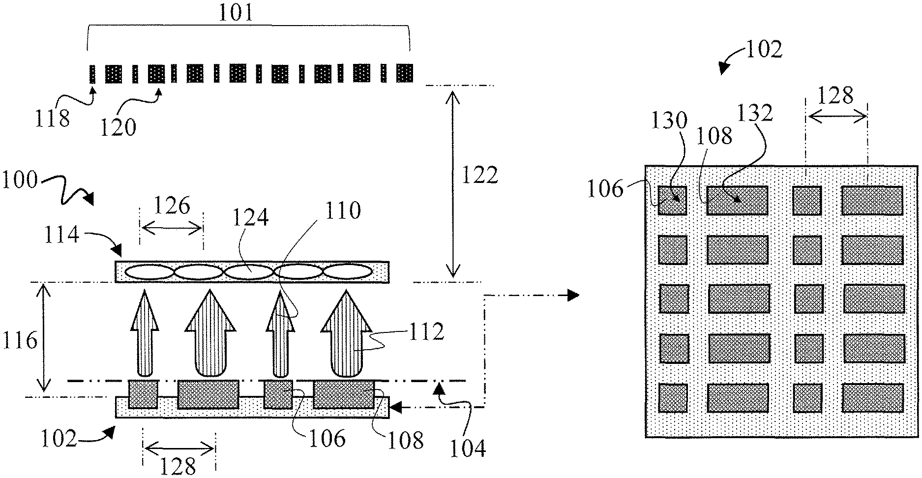
FIG. 1A depicts an example of an illumination module with an example array of light sources.
FIG. 1B depicts a plan-view of the array of light sources depicted in FIG. 1A.
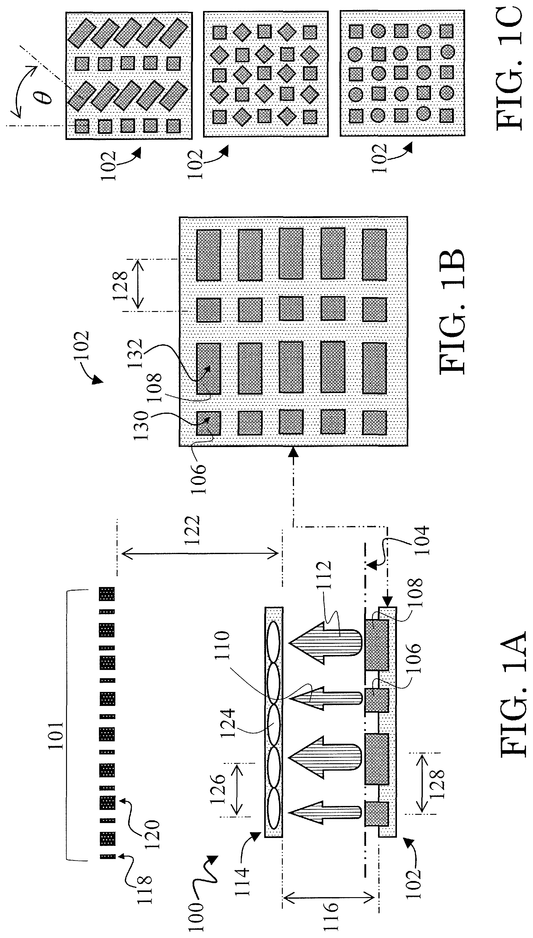
FIG. 1C depicts several alternative arrays of light sources.
FIG. 2 depicts an example of an optoelectronic system.
DETAILED DESCRIPTION
FIG. 1A depicts an example illumination module 100. The illumination module 100 is operable to generate a patterned illumination 101 exhibiting minimal ambiguity. The illumination module 100 can include an array of light sources 102. The array of light source 102 can occur within a common emission plane 104. Each light source can generate light with a near-field intensity profile at the common emission plane 104. The array of light sources can include at least two light sources 106, 108 with different respective near-field intensity profiles 110, 112 at the common emission plane 104. In some instances, the at least two light sources having different near-field intensity profiles 106, 108 can be operable to generate light having different wavelengths and/or ranges of wavelengths (e.g., infrared). In some instances, they may be operable to generate light having the same wavelengths and/or ranges of wavelengths (e.g., infrared).
In some instances, the array of light sources 102 can generate collimated light. In some instances, the array of light sources 102 can include an array of laser diodes. The array of laser diodes can include an array of vertical-cavity surface-emitting lasers, for example.
In some instances, the at least two light sources 106, 108 having different respective near-field intensity profiles 110, 112 can be implemented with different respective apertures 130, 132. The apertures 130, 132 can generate the different respective near-field intensity profiles 110, 112 of the corresponding light sources 106, 108. The different apertures 130, 132 can be intrinsic to the laser diodes corresponding to the light sources 106, 108 (i.e., the apertures 130, 132 may be part of the respective diodes that correspond to light sources 106, 108). In some instances, the illumination module can further include an array of auxiliary apertures. That is, the at least two light sources 106, 108 having different respective near-field intensity profiles 110, 112 can be implemented with the different respective auxiliary apertures aligned with the light sources 106, 108. The auxiliary apertures may be composed, at least in part, of metal foils or dielectric materials.
In some instances, the near-field intensity profiles corresponding to the light sources 106, 108 can be established by an aperture or an auxiliary aperture having a two-dimensional geometric shape such as a square, circle, and/or rectangle. In such instances, the at least two light sources having different respective near-field intensity profiles 106, 108 can be generated from apertures having a square and a rectangular shape, respectively. The square aperture can be 9 microns by 9 microns, for example, while the rectangular aperture can be 3 microns by 27 microns, for example. In some implementations, the at least two light sources having different respective near-field intensity profiles 106, 108 can be established by two apertures that have the same shape but with different respective orientations (as discussed further below).
The illumination module can further include an optical assembly 114 mounted at a distance 116 from the common emission plane 104. The distances 116 can be the optical path length between the optical assembly 114 and the array of light sources 102. The optical assembly 114 and the array of light sources 102 can be operable to substantially replicate the different respective near-field intensity profiles 110, 112 of the at least two light sources 106, 108 in a far-field 122 (e.g., one meter, one to 10 meters or even 10 to 100 meters from the illumination module)--the replicated near-field intensity profiles being the patterned illumination 101. In some instances, the optical assembly 114 and the array of light sources 102 can be operable to substantially replicate the different respective near-field intensity profiles 110, 112 of the at least two light sources 106, 108 in the far-field 122 such that the near-field intensity profiles are contracted, dilated, or magnified in the far field 122 (as patterned illumination 101).
In some instances, the optical assembly 114 can be a microlens array. The microlens array can include a plurality of microlenses 124 respectively arranged at a microlens pitch 126. In some instances, the array 102 of the at least two light sources 106, 108 are respectively arranged at a light-source pitch 128.
In some instances, the microlens pitch 126 can be substantially equal to the square root of the product of the integer 2 divided by an integer greater than or equal to 1, the wavelength and/or range of wavelengths, and the distance (when the wavelengths or ranges of wavelengths of light sources 106, 108 are substantially equal). In some instances, the integer greater than or equal to 1 can be any of the following integers: 1, 2, 3, 4, 5, 6, 7, or 8.
Generally, the microlens array, the distance 116, and the array of light sources can be operable to substantially replicate the different respective near-field intensity profiles of the at least two light sources in a far-field.
FIG. 1B depicts a plan-view of the example array of light sources 102 depicted in FIG. 1A. The at least two light sources 106, 108 having different respective near-field intensity profiles 110, 112 are depicted with different apertures 130, 132, respectively. The light sources 106, 108 are depicted at the light-source pitch 128.
FIG. 1C depicts several alternative example arrays of light sources 102 in plan-view. For example, in some instances, the at least two light sources 106, 108 having different respective near-field intensity profiles 110, 112; or the different apertures 130, 132 responsible for the different respective near-field intensity profiles 110, 112 of the at least two light sources 106, 108; can be positioned about an angle .theta. with respect to each other. In some instances, the at least two light sources 106, 108 having different respective near-field intensity profiles 110, 112; or the different apertures 130, 132 responsible for the different respective near-field intensity profiles 110, 112 of the at least two light sources 106, 108; can be different types of geometric shapes, such as squares and circles. In general, such arrangements (e.g., rotated apertures) of the arrays of light sources 102 can generate a patterned illumination 101 with less ambiguity. In some instances, the angle .theta. can be 40.degree., 45.degree., or 90.degree..
FIG. 2 depicts an example optoelectronic system 2000 operable to generate 3D data. The optoelectronic system 200 can include an illumination module 2100, such as the illumination module 100 depicted in FIG. 1A-FIG. 1C, and can include example features and components as described in connection with the illumination modules 100.
For example, the illumination module 2100 can include an array of light sources having a common emission plane. Each light source can generate light having a near-field intensity profile at the common emission plane. The array of light sources can be respectively arranged at a light-source pitch. The array of light sources can include at least two light sources having different respective near-field intensity profiles at the common emission plane. Further, the illumination module 2100 can include a microlens array mounted at a distance from the common emission plane. The microlens array can include a plurality of microlenses respectively arranged at a microlens pitch. In some instances, the microlens pitch can be substantially equal to the light-source pitch.
The microlens array, the distance, and the array of light sources can be operable to substantially replicate the different respective near-field intensity profiles of the at least two light sources in a far-field, thereby generating a patterned illumination 2200 as depicted in FIG. 2.
In some instances, the patterned illumination 2200 can be an encoded-light pattern. The patterned illumination can be incident on a target 2300. The target can have 3D features, such as a 3D object or a 3D scene. Light reflected form the patterned illumination can be collected by the imager 2400. Further, the imager 2400 can be operable to capture light reflected from the patterned illumination 2200.
The optoelectronic system 200 can further include a processor 2500 communicatively coupled to the illumination module 2100 and the imager 2400, and can also include a non-transitory computer-readable medium 2600 for operating the optoelectronic system 2000. The non-transitory computer-readable medium 2600 includes instructions stored thereon, that when executed on the processor, perform steps for generating the patterned illumination 2200 with the illumination module 2100, capturing light reflected from the patterned illumination with the imager 2400, converting the captured light to signals, and generating 3D data from the signals.
The optoelectronic system 2000 may be implemented as a structured-light imaging system, a stereo-imaging system, or any other 3D imaging system. Still other optoelectronic systems are within the scope of this disclosure, for example, proximity systems having an imager with only a few pixels.
Various modifications can be made within the spirit of the disclosure. Also, features that may be described above in connection with different implementations can be combined in the same implementation in some cases. Accordingly, other implementations are within the scope of the claims.
* * * * *
D00000
D00001
D00002
XML
uspto.report is an independent third-party trademark research tool that is not affiliated, endorsed, or sponsored by the United States Patent and Trademark Office (USPTO) or any other governmental organization. The information provided by uspto.report is based on publicly available data at the time of writing and is intended for informational purposes only.
While we strive to provide accurate and up-to-date information, we do not guarantee the accuracy, completeness, reliability, or suitability of the information displayed on this site. The use of this site is at your own risk. Any reliance you place on such information is therefore strictly at your own risk.
All official trademark data, including owner information, should be verified by visiting the official USPTO website at www.uspto.gov. This site is not intended to replace professional legal advice and should not be used as a substitute for consulting with a legal professional who is knowledgeable about trademark law.