Multi-resonant converter power supply
Arduini , et al. Sep
U.S. patent number 10,763,749 [Application Number 16/191,308] was granted by the patent office on 2020-09-01 for multi-resonant converter power supply. This patent grant is currently assigned to CISCO TECHNOLOGY, INC. The grantee listed for this patent is CISCO TECHNOLOGY, INC.. Invention is credited to Douglas Paul Arduini, Sung Kee Baek, Joel Richard Goergen.

View All Diagrams
| United States Patent | 10,763,749 |
| Arduini , et al. | September 1, 2020 |
Multi-resonant converter power supply
Abstract
In one embodiment, an apparatus includes a first stage comprising a first active switch, a first resonant inductor, and a resonant capacitor and a second stage comprising a second active switch, a second resonant inductor, and a filter capacitor. The first and second stages form a non-isolated multi-resonant converter for converting a DC input voltage to a DC output voltage.
| Inventors: | Arduini; Douglas Paul (San Ramon, CA), Goergen; Joel Richard (Soulsbyville, CA), Baek; Sung Kee (San Ramon, CA) | ||||||||||
|---|---|---|---|---|---|---|---|---|---|---|---|
| Applicant: |
|
||||||||||
| Assignee: | CISCO TECHNOLOGY, INC (San
Jose, CA) |
||||||||||
| Family ID: | 69159947 | ||||||||||
| Appl. No.: | 16/191,308 | ||||||||||
| Filed: | November 14, 2018 |
Prior Publication Data
| Document Identifier | Publication Date | |
|---|---|---|
| US 20200153337 A1 | May 14, 2020 | |
| Current U.S. Class: | 1/1 |
| Current CPC Class: | H02M 1/4241 (20130101); H02M 3/158 (20130101); H02M 3/1582 (20130101); H02M 1/4225 (20130101); H02M 2001/0058 (20130101); Y02B 70/10 (20130101) |
| Current International Class: | H02M 1/42 (20070101); H02M 3/158 (20060101) |
| Field of Search: | ;327/103,541,543 |
References Cited [Referenced By]
U.S. Patent Documents
| 3335324 | August 1967 | Buckeridge |
| 4811187 | March 1989 | Nakajima et al. |
| 5652893 | July 1997 | Ben-Meir |
| 6008631 | December 1999 | Johari |
| 6220955 | April 2001 | Posa |
| 6259745 | July 2001 | Chan |
| 6636538 | October 2003 | Stephens |
| 6685364 | February 2004 | Brezina |
| 6784790 | August 2004 | Lester |
| 6826368 | November 2004 | Koren |
| 6855881 | February 2005 | Khoshnood |
| 6860004 | March 2005 | Hirano |
| 7325150 | January 2008 | Lehr |
| 7420355 | September 2008 | Liu |
| 7490996 | February 2009 | Sommer |
| 7492059 | February 2009 | Peker |
| 7509505 | March 2009 | Randall |
| 7583703 | September 2009 | Bowser |
| 7589435 | September 2009 | Metsker |
| 7593747 | September 2009 | Karam |
| 7603570 | October 2009 | Schindler |
| 7616465 | November 2009 | Vinciarelli |
| 7813646 | October 2010 | Furey |
| 7835389 | November 2010 | Yu |
| 7854634 | December 2010 | Filipon |
| 7881072 | February 2011 | DiBene |
| 7915761 | March 2011 | Jones |
| 7921307 | April 2011 | Karam |
| 7924579 | April 2011 | Arduini |
| 7940787 | May 2011 | Karam |
| 7973538 | July 2011 | Karam |
| 8020043 | September 2011 | Karam |
| 8037324 | October 2011 | Hussain |
| 8081589 | December 2011 | Gilbrech |
| 8184525 | May 2012 | Karam |
| 8276397 | October 2012 | Carlson |
| 8279883 | October 2012 | Diab |
| 8310089 | November 2012 | Schindler |
| 8319627 | November 2012 | Chan |
| 8345439 | January 2013 | Goergen |
| 8350538 | January 2013 | Cuk |
| 8358893 | January 2013 | Sanderson |
| 8700923 | April 2014 | Fung |
| 8712324 | April 2014 | Corbridge |
| 8750710 | June 2014 | Hirt |
| 8781637 | July 2014 | Eaves |
| 8787775 | July 2014 | Earnshaw |
| 8829917 | September 2014 | Lo |
| 8836228 | September 2014 | Xu et al. |
| 8842430 | September 2014 | Hellriegel |
| 8849471 | September 2014 | Daniel |
| 8966747 | March 2015 | Vinciarelli |
| 9019895 | April 2015 | Li |
| 9024473 | May 2015 | Huff |
| 9184795 | November 2015 | Eaves |
| 9189036 | November 2015 | Ghoshal |
| 9189043 | November 2015 | Vorenkamp |
| 9273906 | March 2016 | Goth |
| 9319101 | April 2016 | Lontka |
| 9321362 | April 2016 | Woo |
| 9373963 | June 2016 | Kuznelsov |
| 9419436 | August 2016 | Eaves |
| 9510479 | November 2016 | Vos |
| 9531551 | December 2016 | Balasubramanian |
| 9590811 | March 2017 | Hunter, Jr. |
| 9618714 | April 2017 | Murray |
| 9640998 | May 2017 | Dawson |
| 9665148 | May 2017 | Hamdi |
| 9693244 | June 2017 | Maruhashi |
| 9734940 | August 2017 | McNutt |
| 9853689 | December 2017 | Eaves |
| 9874930 | January 2018 | Vavilala |
| 9882656 | January 2018 | Sipes, Jr. |
| 9893521 | February 2018 | Lowe |
| 9948198 | April 2018 | Imai |
| 9985600 | May 2018 | Xu |
| 10007628 | June 2018 | Pitigoi-Aron |
| 10028417 | July 2018 | Schmidtke |
| 10128764 | November 2018 | Vinciarelli |
| 10248178 | April 2019 | Brooks |
| 10407995 | September 2019 | Moeny |
| 10439432 | October 2019 | Eckhardt |
| 2001/0024373 | September 2001 | Cuk |
| 2002/0126967 | September 2002 | Panak |
| 2004/0000816 | January 2004 | Khoshnood |
| 2004/0033076 | February 2004 | Song |
| 2004/0043651 | March 2004 | Bain |
| 2004/0073703 | April 2004 | Boucher |
| 2004/0264214 | December 2004 | Xu |
| 2005/0197018 | September 2005 | Lord |
| 2005/0268120 | December 2005 | Schindler |
| 2006/0202109 | September 2006 | Delcher |
| 2006/0209875 | September 2006 | Lum |
| 2007/0103168 | May 2007 | Batten |
| 2007/0236853 | October 2007 | Crawley |
| 2007/0263675 | November 2007 | Lum |
| 2007/0284946 | December 2007 | Robbins |
| 2007/0288125 | December 2007 | Quaratiello |
| 2008/0198635 | August 2008 | Hussain |
| 2008/0229120 | September 2008 | Diab |
| 2008/0310067 | December 2008 | Diab |
| 2010/0077239 | March 2010 | Diab |
| 2010/0117808 | May 2010 | Karam |
| 2010/0171602 | July 2010 | Kabbara |
| 2010/0190384 | July 2010 | Lanni |
| 2010/0237846 | September 2010 | Vetteth |
| 2010/0290190 | November 2010 | Chester |
| 2011/0004773 | January 2011 | Hussain |
| 2011/0007664 | January 2011 | Diab |
| 2011/0290497 | January 2011 | Stenevik |
| 2011/0083824 | April 2011 | Rogers |
| 2011/0228578 | September 2011 | Serpa |
| 2011/0266867 | November 2011 | Schindler |
| 2012/0064745 | March 2012 | Ottliczky |
| 2012/0170927 | July 2012 | Huang |
| 2012/0201089 | August 2012 | Barth |
| 2012/0231654 | September 2012 | Conrad |
| 2012/0317426 | December 2012 | Hunter, Jr. |
| 2012/0319468 | December 2012 | Schneider |
| 2013/0077923 | March 2013 | Weem |
| 2013/0079633 | March 2013 | Weem |
| 2013/0103220 | April 2013 | Eaves |
| 2013/0249292 | September 2013 | Blackwell, Jr. |
| 2013/0272721 | October 2013 | Van Veen |
| 2014/0111180 | April 2014 | Vladan |
| 2014/0129850 | May 2014 | Paul |
| 2014/0258742 | September 2014 | Chien |
| 2014/0265550 | September 2014 | Milligan |
| 2014/0372773 | December 2014 | Heath |
| 2015/0078740 | March 2015 | Sipes, Jr. |
| 2015/0106539 | April 2015 | Leinonen |
| 2015/0115741 | April 2015 | Dawson |
| 2015/0215001 | July 2015 | Eaves |
| 2015/0215131 | July 2015 | Paul |
| 2015/0333918 | November 2015 | White, III |
| 2015/0340818 | November 2015 | Scherer |
| 2016/0020911 | January 2016 | Sipes, Jr. |
| 2016/0064938 | March 2016 | Balasubramanian |
| 2016/0111877 | April 2016 | Eaves |
| 2016/0118784 | April 2016 | Saxena |
| 2016/0133355 | May 2016 | Glew |
| 2016/0134331 | May 2016 | Eaves |
| 2016/0142217 | May 2016 | Gardner |
| 2016/0197600 | July 2016 | Kuznetsov |
| 2016/0365967 | July 2016 | Tu |
| 2016/0241148 | August 2016 | Kizilyalli |
| 2016/0262288 | September 2016 | Chainer |
| 2016/0273722 | September 2016 | Crenshaw |
| 2016/0294500 | October 2016 | Chawgo |
| 2016/0308683 | October 2016 | Pischl |
| 2016/0352535 | December 2016 | Hiscock |
| 2017/0041152 | February 2017 | Sheffield |
| 2017/0041153 | February 2017 | Picard |
| 2017/0054296 | February 2017 | Daniel |
| 2017/0110871 | April 2017 | Foster |
| 2017/0123466 | May 2017 | Carnevale |
| 2017/0146260 | May 2017 | Ribbich |
| 2017/0155517 | June 2017 | Cao |
| 2017/0164525 | June 2017 | Chapel |
| 2017/0155518 | July 2017 | Yang |
| 2017/0214236 | July 2017 | Eaves |
| 2017/0229886 | August 2017 | Eaves |
| 2017/0234738 | August 2017 | Ross |
| 2017/0244318 | August 2017 | Giuliano |
| 2017/0248976 | August 2017 | Moller |
| 2017/0325320 | November 2017 | Wendt |
| 2018/0024964 | January 2018 | Mao |
| 2018/0053313 | February 2018 | Smith |
| 2018/0054083 | February 2018 | Hick |
| 2018/0060269 | March 2018 | Kessler |
| 2018/0088648 | March 2018 | Otani |
| 2018/0098201 | April 2018 | Torello |
| 2018/0102604 | April 2018 | Keith |
| 2018/0123360 | May 2018 | Eaves |
| 2018/0159430 | June 2018 | Albert |
| 2018/0188712 | July 2018 | MacKay |
| 2018/0191513 | July 2018 | Hess |
| 2018/0254624 | September 2018 | Son |
| 2018/0313886 | November 2018 | Mlyniec |
| 2019/0267804 | August 2019 | Matan |
| 2019/0280895 | September 2019 | Mather |
| 1209880 | Jul 2005 | CN | |||
| 201689347 | Dec 2010 | CN | |||
| 204836199 | Dec 2015 | CN | |||
| 205544597 | Aug 2016 | CN | |||
| 104081237 | Oct 2016 | CN | |||
| 104412541 | May 2019 | CN | |||
| 1936861 | Jun 2008 | EP | |||
| 2120443 | Nov 2009 | EP | |||
| 2693688 | Feb 2014 | EP | |||
| WO199316407 | Aug 1993 | WO | |||
| WO2010053542 | May 2010 | WO | |||
| WO2017054030 | Apr 2017 | WO | |||
| WO2017167926 | Oct 2017 | WO | |||
| WO2018017544 | Jan 2018 | WO | |||
| WO2019023731 | Feb 2019 | WO | |||
Other References
|
https://www.fischerconnectors.com/us/en/products/fiberoptic. cited by applicant . http://www.strantech.com/products/tfoca-genx-hybrid-2.times.2-fiber-optic-- copper-connector/. cited by applicant . http://www.qpcfiber.com/product/connectors/e-link-hybrid-connector/. cited by applicant . https://www.lumentum.com/sites/default/files/technical-library-items/power- overfiber-tn-pv-ae_0.pdf. cited by applicant . "Network Remote Power Using Packet Energy Transfer", Eaves et al., www.voltserver.com, Sep. 2012. cited by applicant . Product Overview, "Pluribus VirtualWire Solution", Pluribus Networks, PN-PO-VWS-05818, https://www.pluribusnetworks.com/assets/Pluribus-VirtualWire-PO-50918.pdf- , May 2018, 5 pages. cited by applicant . Implementation Guide, "Virtual Chassis Technology Best Practices", Juniper Networks, 8010018-009-EN, Jan 2016, https://wwwjuniper.net/us/en/local/pdf/implementation-guides/8010018-en.p- df, 29 pages. cited by applicant . Yencheck, Thermal Modeling of Portable Power Cables, 1993. cited by applicant . Zang, Machine Learning-Based Temperature Prediction for Runtime Thermal Management across System Components, Mar. 2016. cited by applicant . Data Center Power Equipment Thermal Guidelines and Best Practices. cited by applicant . Dynamic Thermal Rating of Substation Terminal Equipment by Rambabu Adapa, 2004. cited by applicant . Chen, Real-Time Termperature Estimation for Power MOSEFETs Conidering Thermal Aging Effects:, IEEE Trnasactions on Device and Materials Reliability, vol. 14, No. 1, Mar. 2014. cited by applicant . Jingquan Chen et al: "Buck-boost PWM converters having two independently controlled switches", 32nd Annual IEEE Power Electronics Specialists Conference. PESC 2001. Conference Proceedings, Vancouver, Canada, Jun. 17-21, 2001; [Annual Power Electronics Specialists Conference], New York, NY: IEEE, US, vol. 2, Jun. 17, 2001 (Jun. 17, 2001), pp. 736-741, XP010559317, DOI: 10.1109/PESC.2001.954206, ISBN 978-0-7803-7067-8 paragraph [SectionII]; figure 3. cited by applicant . Cheng K W E et al: "Constant Frequency, Two-Stage Quasiresonant Convertor", IEE Proceedings B. Electrical Power Applications, 1271980 1, vol. 139, No. 3, May 1, 1992 (May 1, 1992), pp. 227-237, XP000292493, the whole document. cited by applicant. |
Primary Examiner: Hernandez; William
Attorney, Agent or Firm: Kaplan; Cindy
Claims
What is claimed is:
1. An apparatus comprising: a first stage comprising a first active switch, a first resonant inductor, and a resonant capacitor; and a second stage comprising a second active switch, a second resonant inductor, and a filter capacitor; wherein said first and second stages form a non-isolated multi-resonant converter for converting a DC input voltage to a DC output voltage and the apparatus comprises an input isolation stage.
2. The apparatus of claim 1 wherein the non-isolated multi-resonant converter comprises a step-down voltage converter.
3. The apparatus of claim 1 wherein the non-isolated multi-resonant converter comprises a step-up voltage converter.
4. The apparatus of claim 1 wherein at least one of said stages comprises a synchronous rectifier.
5. The apparatus of claim 1 wherein each of said stages comprises a synchronous rectifier.
6. The apparatus of claim 1 wherein said first and second resonant inductors operate with currents in discontinuous mode and wherein a voltage at the resonant capacitor discharges to zero on each of a plurality of cycles.
7. The apparatus of claim 1 wherein said first and second resonant inductors operate with currents in continuous mode and wherein a voltage at the resonant capacitor discharges other than zero on each of a plurality of cycles.
8. The apparatus of claim 1 wherein said first stage and said second stage operate in discontinuous current mode with switch zero-current turn-on.
9. The apparatus of claim 1 wherein the apparatus is operable to use frequency modulation to regulate output voltage and current.
10. The apparatus of claim 1 wherein said first stage is configured to use pulse width modulation to regulate a charge stored on the resonant capacitor to regulate output voltage and current.
11. The apparatus of claim 1 wherein said second resonant inductor comprises a tapped inductor.
12. An apparatus comprising: a first stage comprising a first active switch, a first resonant inductor, and a resonant capacitor; and a second stage comprising a second active switch, a second resonant inductor, and a filter capacitor; wherein said first and second stages form a non-isolated multi-resonant converter for converting a DC input voltage to a DC output voltage and the apparatus comprises a power factor correction stage.
13. The apparatus of claim 12 wherein the non-isolated multi-resonant converter comprises a step-down voltage converter.
14. The apparatus of claim 12 wherein the non-isolated multi-resonant converter comprises a step-up voltage converter.
15. An apparatus comprising: a card for insertion into a network device, the card comprising a point-of-load power supply comprising: a first stage comprising a first switch, a first inductor, and a resonant capacitor; and a second stage comprising a second switch, a second inductor, and a filter capacitor; wherein said first stage comprises a power regulation resonant stage and said second stage comprises a voltage converter resonant stage to form a non-isolated multi-resonant converter and the apparatus comprises an input isolation stage.
16. The apparatus of 14 wherein the point-of-load power supply eliminates a need for an intermediate bus converter on the card.
17. The apparatus of claim 15 wherein at least one of said stages comprises a synchronous rectifier.
18. The apparatus of claim 15 wherein said second inductor comprises a tapped resonant inductor.
19. The apparatus of claim 15 wherein said first stage is configured to use pulse width modulation or frequency modulation to regulate output voltage and current.
20. A point-of-load power supply comprising: a first stage comprising a first active switch, a resonant inductor, and a resonant capacitor; and a second stage comprising a second active switch, a tapped resonant inductor, and a filter capacitor; wherein said first stage and said second stage form a non-isolated multi-resonant converter for converting a DC input voltage to a DC output voltage with a step-down voltage conversion or a step-up voltage conversion; and wherein the point-of-load power supply comprises a power factor correction stage.
Description
TECHNICAL FIELD
The present disclosure relates generally to voltage converters, and more particularly, to multi-resonant converters.
BACKGROUND
DC-to-DC converters are used to convert a DC voltage at one level to a DC voltage at another level and deliver power to a load. Such convertors typically comprise a transformer, which provides power transfer from input to output as a voltage converter. The transformer may also provide galvanic isolation between input and output in most applications. In conventional resonant topologies, a transformer is typically needed for wide voltage conversion ranges from input to output for good efficiency. Use of a transformer, however, limits the switching frequency due to core loss at higher frequencies and has additional drawbacks such as complex circuitry, large size, and high cost.
BRIEF DESCRIPTION OF THE DRAWINGS
FIG. 1 illustrates an example of a step-down Multi-Resonant Converter (MRC), in accordance with one embodiment.
FIG. 2 illustrates operation of the MRC shown in FIG. 1.
FIG. 3 illustrates an example of a high voltage-ratio step-down MRC, in accordance with one embodiment.
FIG. 4 illustrates operation of the MRC shown in FIG. 3.
FIG. 5 illustrates additional detail of operation of the MRC shown in FIG. 3 in a power storage stage and power transfer stage.
FIG. 6 illustrates an example of an MRC step-down-up buck-boost, in accordance with one embodiment.
FIG. 7 illustrates operation of the MRC shown in FIG. 6.
FIG. 8A illustrates an example of an MRC step-up-down boost-buck, in accordance with one embodiment.
FIG. 8B illustrates an example of an MRC step-up boost-boost, in accordance with one embodiment.
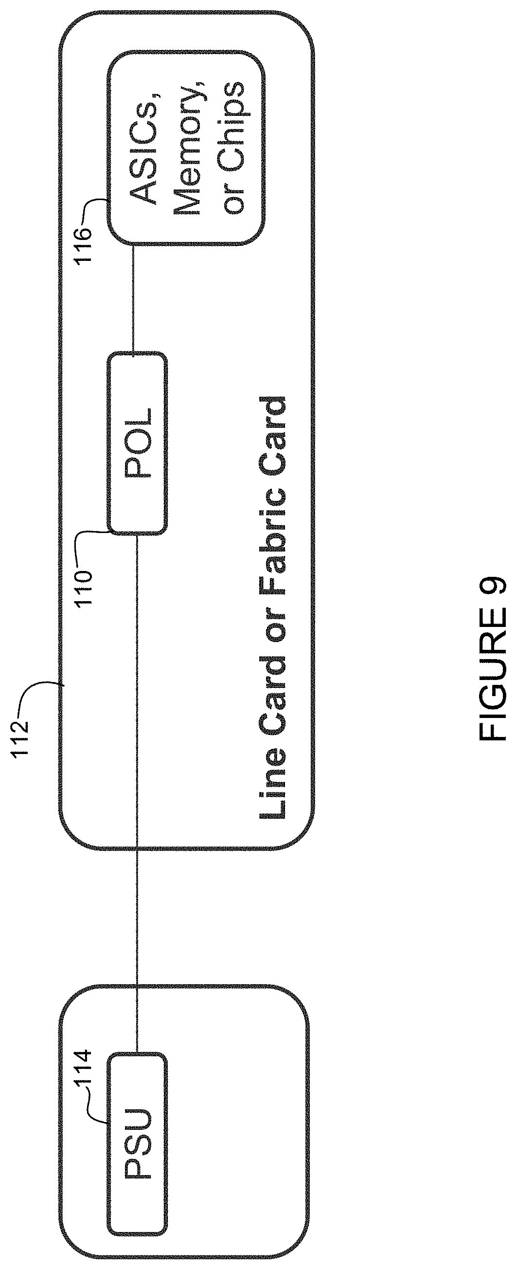
FIG. 9 is a block diagram illustrating implementation of the MRC as a point-of-load power supply on a line card or fabric card, in accordance with one embodiment.
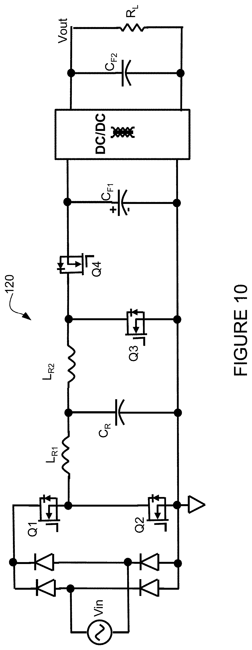
FIG. 10 is an example illustrating implementation of the MRC topology of FIG. 6 in an AC/DC PFC (Power Factor Correction) MRC stage to isolated DC/DC converter.
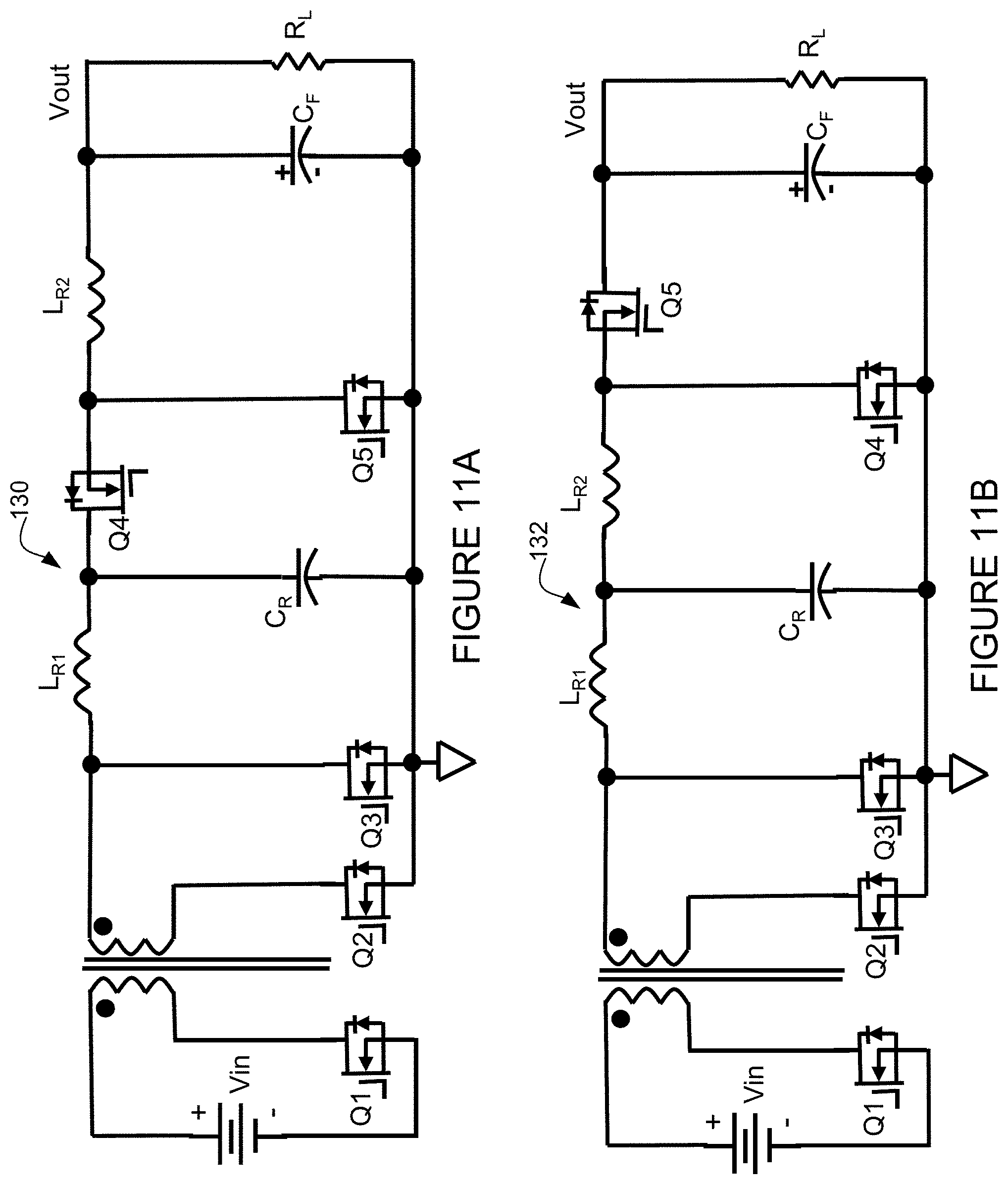
FIG. 11A is an example illustrating implementation of the step-down MRC topology of FIG. 1 in a DC/DC isolated MRC with a forward converter transformer stage.
FIG. 11B is an example illustrating implementation of the step-up MRC topology of FIG. 6 in a DC/DC isolated MRC with a forward converter transformer stage.
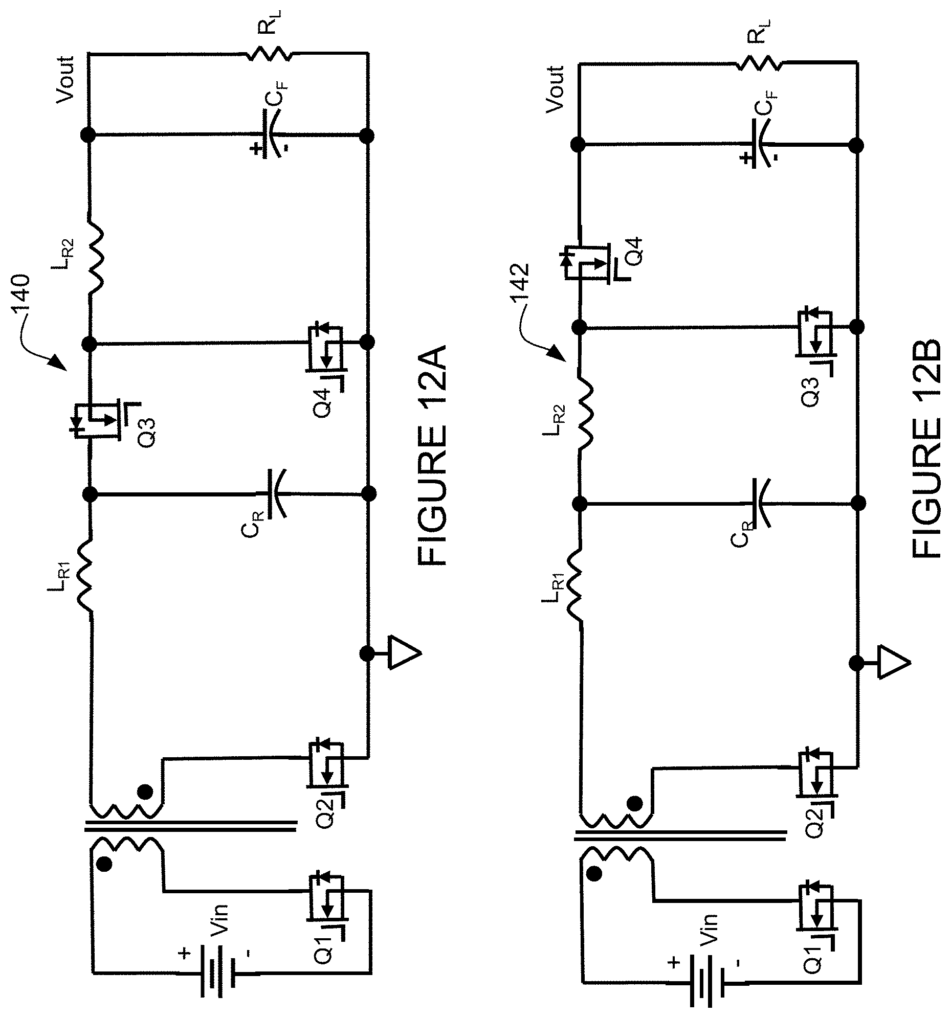
FIGS. 12A and 12B are examples illustrating implementation of an isolated MRC with flyback PWM of the resonant capacitor and a second resonant switched stage with a synchronous rectifier.
Corresponding reference characters indicate corresponding parts throughout the several views of the drawings.
DESCRIPTION OF EXAMPLE EMBODIMENTS
Overview
In one embodiment, an apparatus generally comprises a first stage comprising a first active switch, a first resonant inductor, and a resonant capacitor and a second stage comprising a second active switch, a second resonant inductor, and a filter capacitor. The first and second stages form a non-isolated multi-resonant converter topology for converting a DC input voltage to a DC output voltage.
The non-isolated multi-resonant converter may comprise a step-down converter or a step-up converter. In one or more embodiments, one or both stages comprise a synchronous rectifier. In one or more embodiments, the first and second resonant inductors operate with currents in discontinuous mode and a voltage at the resonant capacitor discharges to zero on each of a plurality of cycles. In one or more embodiments, both stages operate in discontinuous current mode with zero-current turn-on, the first stage operating at zero-current turn-off at a maximum duty cycle, and the second stage operating at zero-current turn-off at ninety degrees of a half-sine transfer pulse current. In one or more embodiments, the first stage is configured to use pulse width modulation or frequency modulation to regulate a charge stored on the resonant capacitor to regulate output voltage and current. In one or more embodiments, the second resonant inductor comprises a tapped inductor.
In another embodiment, an apparatus generally comprises a card for insertion into a network device, the card comprising a point-of-load power supply comprising a first stage comprising a first switch, a first inductor, and a resonant capacitor and a second stage comprising a second switch, a second inductor, and a filter capacitor. The first stage comprises a power regulation resonant stage and the second stage comprises a voltage converter stage to form a non-isolated multi-resonant converter.
In yet another embodiment, an apparatus generally comprises a point-of-load power supply comprising a first stage comprising a first active switch, a resonant inductor, and a resonant capacitor and a second stage comprising a second active switch, a tapped resonant inductor, and a filter capacitor. The first stage and second stage form a non-isolated multi-resonant converter for converting a DC input voltage to a DC output voltage with a step-down voltage conversion with a large input-to-output ratio example of 48 volts to 1 volt or a step-up voltage conversion with a large input-to-output ratio example of 48 volts to 400 volts.
Further understanding of the features and advantages of the embodiments described herein may be realized by reference to the remaining portions of the specification and the attached drawings.
Example Embodiments
The following description is presented to enable one of ordinary skill in the art to make and use the embodiments. Descriptions of specific embodiments and applications are provided only as examples, and various modifications will be readily apparent to those skilled in the art. The general principles described herein may be applied to other applications without departing from the scope of the embodiments. Thus, the embodiments are not to be limited to those shown, but are to be accorded the widest scope consistent with the principles and features described herein. For purpose of clarity, details relating to technical material that is known in the technical fields related to the embodiments have not been described in detail.
One or more embodiments described herein provide a two-stage, two-switch, multi-resonant voltage converter operable to provide wide-range (high voltage conversion ratio) input-to-output voltages, step-up or step-down, without a transformer for higher frequency, and high efficiency with fewer parts, smaller space requirements, and lower cost. As described in detail below, the topology combines a resonant or quasi-resonant first stage for power regulation and a second stage that acts as a voltage converter thereby enabling a wide voltage conversion range with high efficiency. In one or more embodiments, the topology may provide a DC/DC non-isolated power supply comprising a two-stage, two-switch multi-resonant converter (MRC) with quasi-resonant or full-resonant operation in one or both stages that provides voltage conversion over wide voltage ratios of up-conversion or down-conversion at high efficiency.
The embodiments described herein provide higher frequency and efficiency with fewer components for high power density. In one or more embodiments, higher efficiency is provided with soft switching resonant or quasi-resonant charging and discharging stages and higher frequency is provided without transformers typically needed for high voltage ratio conversion for step-down or step-up converters. Soft-switching in most phases provides high efficiency and lower stresses on switches and components.
As previously noted, one or more embodiments provide large voltage conversion ratios as a down-converter or up-converter without a transformer or losses in performance. Thus, a high voltage-ratio step-down or step-up converter may be implemented using the embodiments described herein without the need for a transformer. By eliminating the need for a transformer for wide voltage conversion, very high frequencies may be used with smaller size packages and higher efficiency. In one or more embodiments, the converter provides flexible voltage or current regulation including pulse width modulation (PWM), frequency modulation (FM), or both pulse width modulation and frequency modulation.
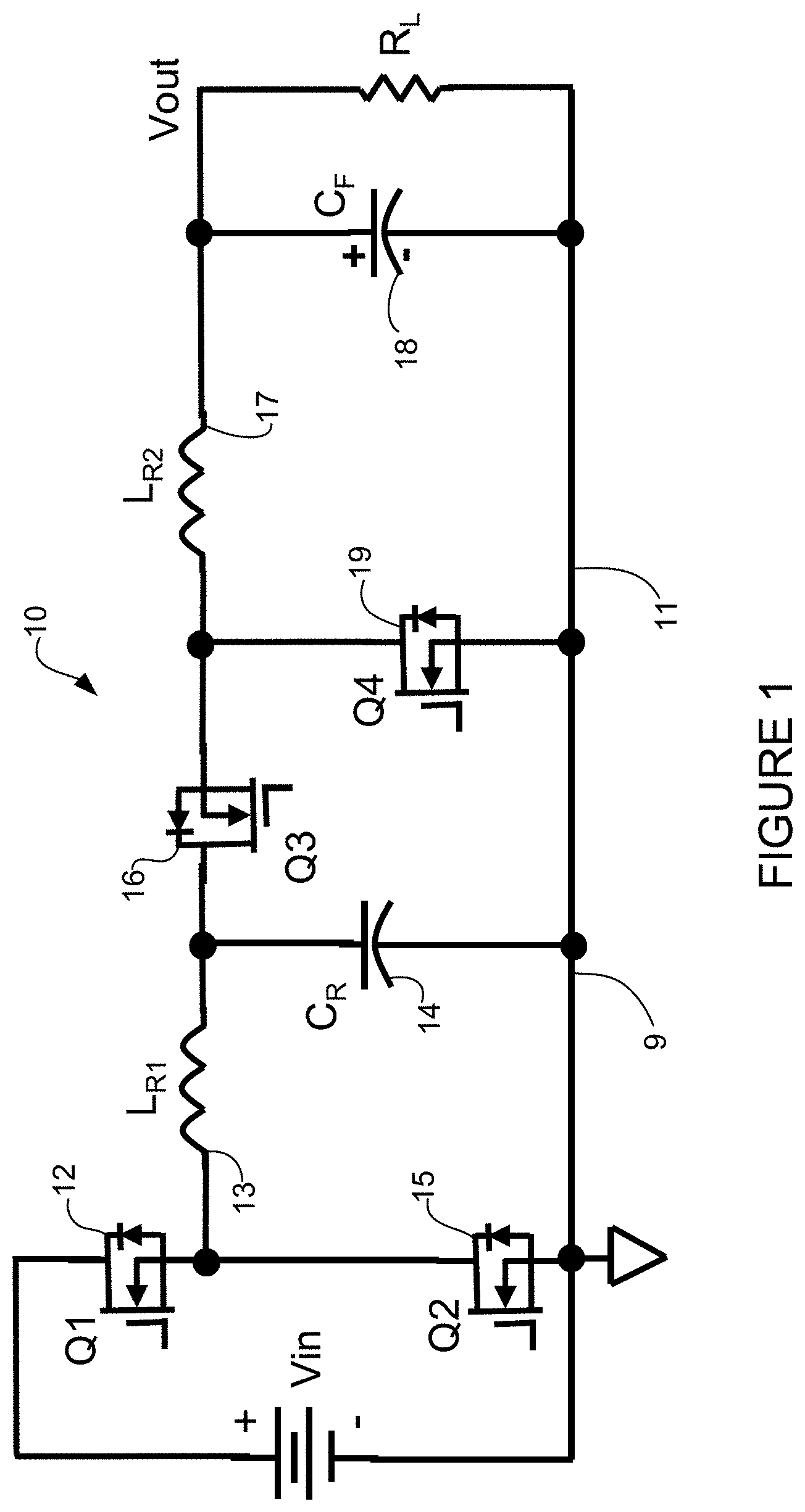
Referring now to the drawings, and first to FIG. 1, an example of a multi-resonant converter (MRC) power supply circuit, generally indicated at 10, is shown in accordance with one embodiment. In the example shown in FIG. 1, the MRC 10 is a two-stage, two-switch resonant-buck-buck converter. A first stage 9 comprises a first active switch 12 (Q1), a first resonating inductor 13 (L.sub.R1), a resonant capacitor 14 (C.sub.R), and a first synchronous rectifier 15 (Q2). A second stage 11 comprises a second active switch 16 (Q3), a second resonating inductor 17 (L.sub.R2), a filter capacitor 18 (C.sub.F), and a second synchronous rectifier 19 (Q4). A DC input voltage V.sub.in (DC voltage source) is converted to a DC output voltage to be imposed across a load represented by resistor R.sub.L. The first inductor L.sub.R1 is electrically coupled in series with the first switch Q1 and the resonant capacitor C.sub.R. The second inductor L.sub.R2 is electrically coupled in series with the second switch Q3 and the filter capacitor C.sub.F. The synchronous rectifiers Q2 and Q4 are in parallel with the capacitors C.sub.R and C.sub.F. The resistor R.sub.L is connected in parallel with the capacitor C.sub.F to form a load. As described in detail below, resonant power transfer is provided between an input LC charge storage stage (first stage 9) to output voltage conversion stage (second stage 11) to output capacitor C.sub.F and load R.sub.L. The first and second stages form a non-isolated multi-resonant converter for converting a DC input voltage to a DC output voltage.
The switches Q1 and Q3 and synchronous rectifiers Q2 and Q4 may comprise any suitable actively controlled switching device (active switch) capable of operating at the desired switching frequency, such as a Metal Oxide semiconductor Field Effect Transistor (MOSFET), a Bipolar Junction Transistor (BJT), a Gallium Nitride Field Effect Transistor (GaNFET), or a solid state relay (SSR). Closing and opening of the switches may be managed by control logic coupled to the switch (not shown). The control logic may be part of a processor or a separate integrated circuit such as a pulse width modulation (PWM) controller. The voltage step-down for the MRC topology shown in FIG. 1 may be, for example, 50 volts to 25 volts (50:25V) or other suitable ratio.
The MRC 10 generally stores an energy voltage charge from the input voltage V.sub.in to C.sub.R and transfers that energy charge to the output filter and load with a power transfer function at P.sub.in=1/2C.sub.R V.sub.CR.sup.2 F, where Pin is the input power, V.sub.CR is a capacitance peak voltage charge, C.sub.R is the resonant capacitance, and F is a switching frequency. The first LC resonant stage switch Q1 charges the resonant capacitor C.sub.R with a stored power pulse from the input voltage V.sub.in in a first half-sine period of the switching frequency, as described below with respect to FIG. 2. The second LC resonant stage switch Q3 then transfers the stored power in the resonant capacitor C.sub.R as a voltage converter in the output filter capacitor C.sub.F and load R.sub.L at high frequency. The resonant inductor current typically operates at a discontinuous mode and the resonant capacitor voltage discharges to zero minimum voltage on each cycle with discontinuous current operation (see V.sub.CR trace in FIG. 2). This may require that the second stage discharge switch duty cycle be adjusted or modulated at less than 90-degrees switching cycle. But there are other possible control modes where the minimum voltage on C.sub.R is above or below zero on each switching cycle and with discontinuous or continuous current operation where the second stage discharge switch duty cycle may be adjusted to more or less than 90-degrees switching cycle and the synchronous rectifier may be eliminated.
It is to be understood that the MRC power supply topology shown in FIG. 1 is only an example and that modifications may be made to the circuit without departing from the scope of the embodiments. For example, one or both of the synchronous rectifiers Q2, Q4 may be removed. Also, the inductor L.sub.R2 may be replaced with a tapped inductor, as described below with respect to FIG. 3. The circuit may also be modified to provide step-up conversion, as described below with respect to FIGS. 8, 10A, and 10B. Typically the minimum voltage on C.sub.R is zero on each cycle with discontinuous current operation, but is some control applications this may require that the second stage discharge switch duty cycle be adjusted or modulated at less than 90-degrees switching cycle. But there are other possible control modes where the minimum voltage on C.sub.R is above or below zero on each switching cycle and with discontinuous or continuous current operation where the second stage discharge switch duty cycle may be adjusted to more or less than 90-degrees switching cycle and the synchronous rectifier may be eliminated. Also, in one or more embodiments, the circuit may include an input isolation stage and the input isolation stage may be part of the input switching stage.
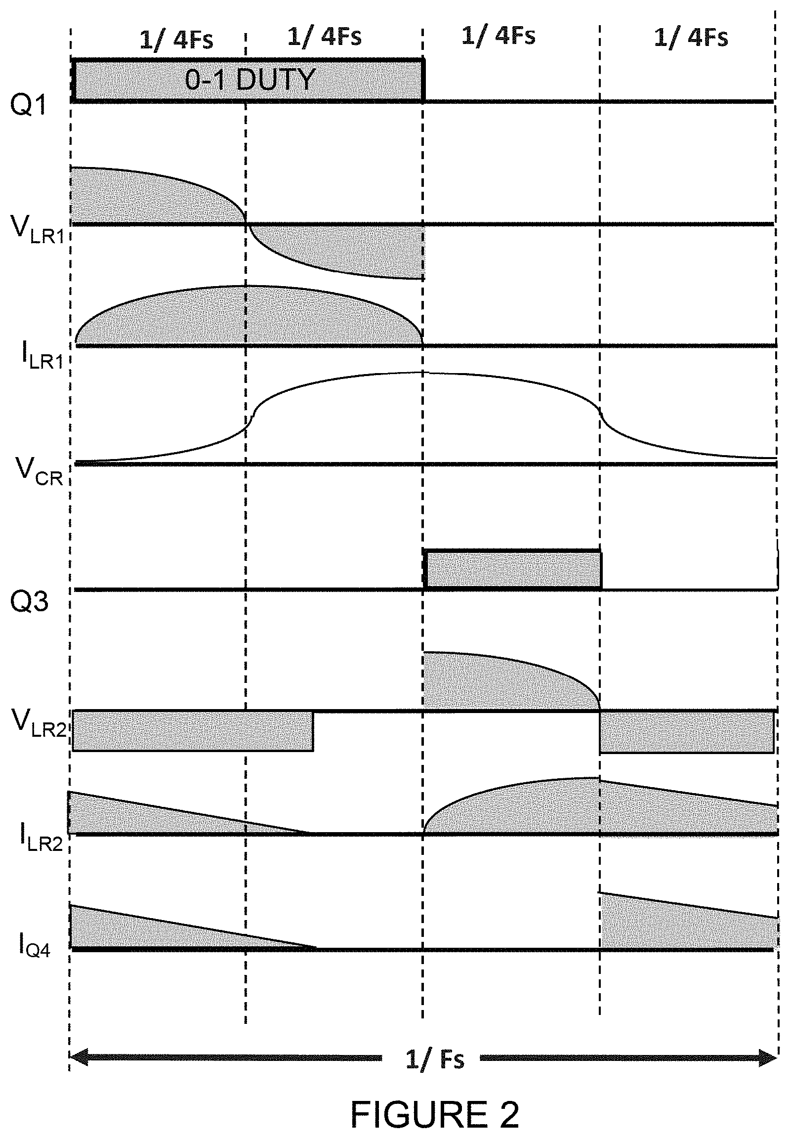
FIG. 2 illustrates step-down MRC operation for the converter 10 shown in FIG. 1. Q1 and Q3 traces in FIG. 2 illustrate the on/off states of the switches. Q1 in FIG. 2 is the duty cycle power charge switch and Q3 is the power transfer switch. Q2 and Q4 are synchronous rectifiers with Q2 a synchronous rectifier only for Q1 Duty.sub.(0-0.5) modulation. The voltage and current at L.sub.R1 are shown at V.sub.LR1 and I.sub.LR1, respectively. The voltage and current at L.sub.R2 are shown at V.sub.LR2 and I.sub.LR2, respectively. V.sub.CR illustrates the charge and discharge at C.sub.R. The resonant capacitor C.sub.R will charge to two times V.sub.in at full-duty cycle. The input switch Q1 is modulated as 0-50%/cycle (duty cycle) of resonant input charge cycle with zero-current on-switching to modulate C.sub.R with 0-2 times input voltage through L.sub.R1 current (I.sub.LR1).
In this example, the first LC resonant switched stage 9 operates in a discontinuous current mode with zero-current turn-on and zero-current turn-off at the maximum duty cycle of 50% of the switching frequency as a resonant half-cycle (FIGS. 1 and 2). The first LC switch resonant stage 9 may use pulse-width-modulation (PWM) over the 0-50% duty cycle to regulate the voltage charge stored on the resonant capacitor C.sub.R to regulate the output voltage and current. During PWM switching, less than the 50% of the maximum duty cycle will turn-off with interrupting current with use of a synchronous rectifier for the first resonant inductor. Another method for regulating the output voltage and current uses frequency-modulation (FM) below the resonant switching maximum frequency. A combination of both PWM and FM may also be used.
In this example, the second CL resonant switched stage 11 operates in a discontinuous current mode with zero-current turn-on, but turn-off at 90-degrees of the half-sine transfer pulse current where the synchronous rectifier clamps the current back to the output filter capacitor C.sub.F and load R.sub.L. The first 1/2-cycle of energy storage and the second 1/2-cycle of energy transfer and voltage conversion complete one power cycle at the switching frequency. The output switch Q3 is fixed for 25%/cycle resonant output discharge 1/2-cycle with zero-current on-switching and transfers energy in L.sub.R2 charging current into filter capacitor (output capacitor) C.sub.F and load R.sub.L. This allows all of the energy storage in C.sub.R to be transferred to the output and to leave the voltage on C.sub.R at zero volts for the next charge cycle. The output inductor L.sub.R2 may have, for example, a 25%/cycle linear output discharge of L.sub.R2 current (I.sub.LR2) charging into the output capacitor C.sub.F and load R.sub.L.
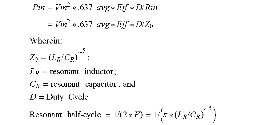
The following are examples of MRC power transfer functions for the circuit shown in FIG. 1 and operation shown in FIG. 2: Pin=1/2*C.sub.R*V.sub.CR.sup.2*F.sub.s Wherein: C.sub.R=resonant capacitor; V.sub.CR=capacitor peak charge voltage; and F.sub.s=switching frequency.
In one example input power is defined as follows:
.times..times..times..times..times..times..times..times..times..times. ##EQU00001## ##EQU00001.2## .times..times. ##EQU00001.3## ##EQU00001.4## ##EQU00001.5## ##EQU00001.6## .times..times..times..times..pi..times..times. ##EQU00001.7##
The first stage 9 provides energy storage in the resonant capacitor C.sub.R in a first half-cycle of the switching period. This energy represents the power input for each cycle and may be modulated by PWM or FM, as previously noted, for output voltage and current regulation. The second stage 11 provides energy transfer from the resonant capacitor C.sub.R to the output filter capacitor C.sub.F and the load resistance R.sub.L. The second stage 11 is also the voltage conversion stage as a voltage down-converter (or up-converter as described below) and controlled by the output resistance. Output power may be defined as follows: Pout=Pin*Eff Vout=(Pout*R.sub.L){circumflex over ( )}.sup.5 V.sub.CR=2*Vin*sin(Duty.sub.(0-1)*90.degree.) Wherein: Duty.sub.(0-1)=T.sub.Q1_ON/0.5T.sub.Fs_period C.sub.R=Pout*max Duty.sub.(0-0.5)*Eff/(0.5*V.sub.CR.sup.2*Fs) L.sub.R=(t.sub.R/.pi.).sup.2/C.sub.R) Wherein t.sub.R=resonant half-sine at 1/2 Fs C.sub.F=i*1/Fs/dv Wherein i=Iout; Fs=switching frequency; and dv=Vp-p ripple
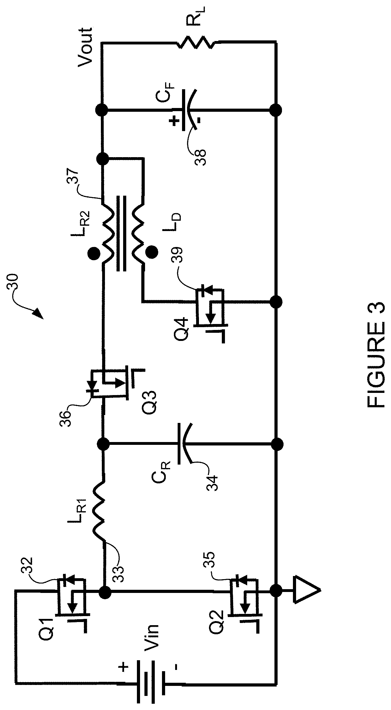
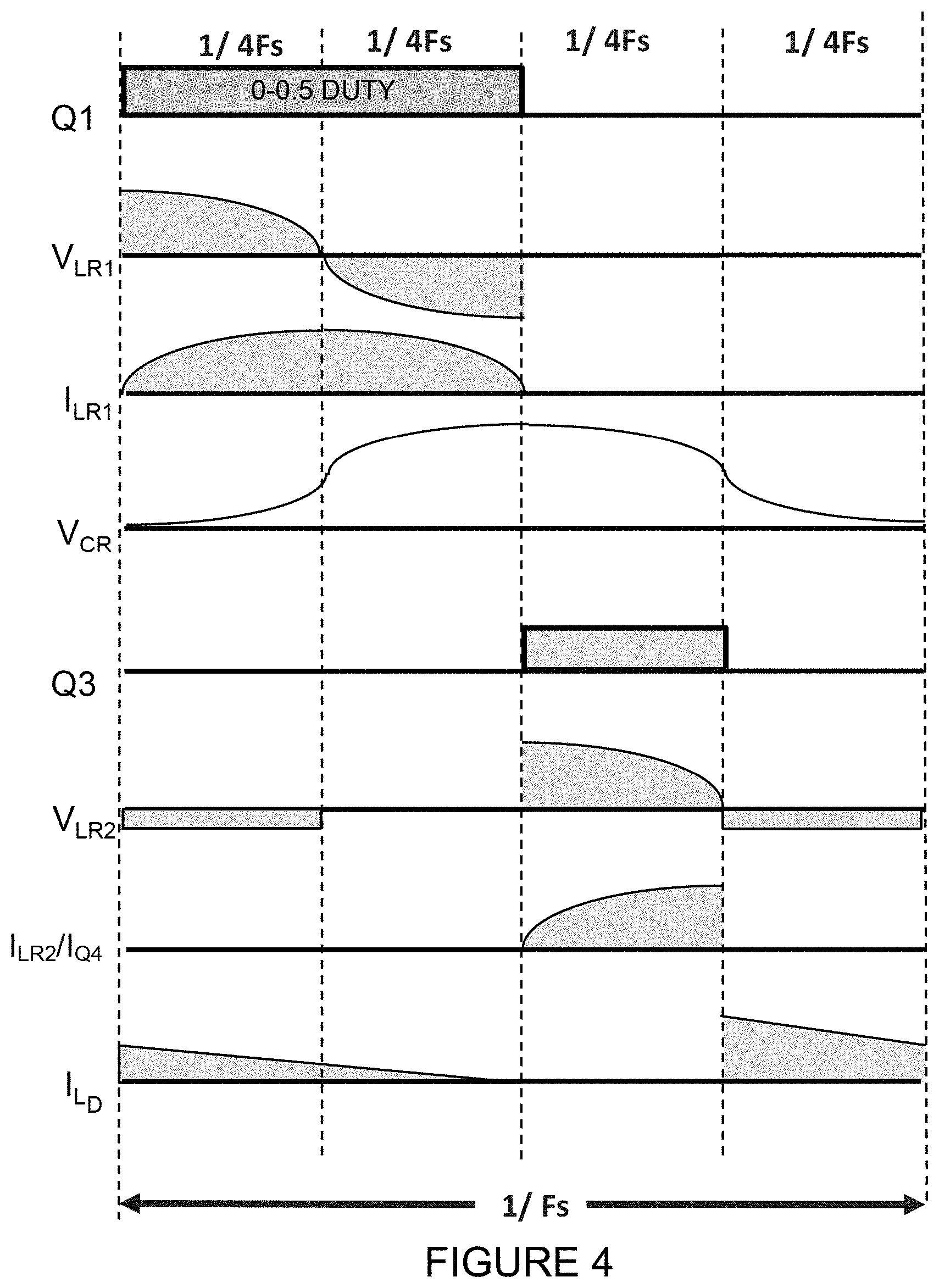
FIG. 3 illustrates a DC/DC resonant-buck-buck high voltage-ratio step-down MRC non-isolated power supply converter, generally indicated at 30. In this example, the second stage inductor L.sub.R2 is replaced with a tapped inductor L.sub.R2/L.sub.D. L.sub.R2 is the resonant choke for the power transfer voltage converter stage to the output filter capacitor and the load resistor. L.sub.D is the tapped inductor winding of resonant choke L.sub.R2 for the current reset cycle with Q4 synchronous rectifier that resets linearly at the lower output voltage. The split inductor provides a high voltage-ratio where the L.sub.D inductance is much smaller than L.sub.R2 inductance to allow less time for the L.sub.R2 current reset cycle with the very low output voltage on L.sub.D compared to the higher voltage that was across L.sub.R2 during the Q3 discharge 1/4-cycle. In one example, the DC/DC step-down MRC 30 shown in FIG. 3 provides a 48 volts to 1 volt ratio (48:1V), 50:5V, or any other suitable step-down POL converter high voltage-ratio with high efficiency.
FIG. 4 illustrates step-down MRC operation for the converter 10 shown in FIG. 3. Q1 and Q3 traces in FIG. 4 illustrate the on/off states of the switches. Q1 in FIG. 2 is the duty cycle power charge and Q3 is the power transfer. Q2 and Q4 are synchronous rectifiers with Q2 a synchronous rectifier only for Q1 Duty.sub.(0-0.5) modulation. The voltage and current are shown for L.sub.R1 at V.sub.LR1 and I.sub.LR1, respectively. Current is shown for L.sub.R2 relative to synchronous rectifier Q4 at I.sub.Lr2 and for L.sub.D at I.sub.LD. V.sub.CR illustrates the charge and discharge at C.sub.R.
Power and voltage may be calculated as previously described with respect to FIG. 1. L.sub.D may be defined as follows: L.sub.D=e*1.5t.sub.R*0.5/di Wherein: e=Vout; di=Iout/(Duty.sub.(0-0.25)*0.5 for average)
FIG. 5 illustrates power storage and voltage conversion stages in the MRC power supply topology shown in FIG. 3 with a duty cycle of 0-100% in a first 1/2 cycle. Mode 1 and Mode 2 make up the resonant charge power storage stage. Mode 1 illustrates the power storage duty cycle maximum period with V.sub.in into L.sub.R1/C.sub.R through Q1 for charge I.sub.LR1. Mode 2 covers the power storage maximum period for discharge L.sub.LR1 to C.sub.R after duty cycle with synchronous rectifier Q2. Mode 3 and Mode 4 make up the power transfer to voltage conversion stage. Mode 3 illustrates the resonant discharge of C.sub.R into L.sub.R2/C.sub.F through Q3 for charge I.sub.LR2. Mode 4 shows a linear discharge of L.sub.R2/L.sub.D for discharge I.sub.LR2 with synchronous rectifier Q4.
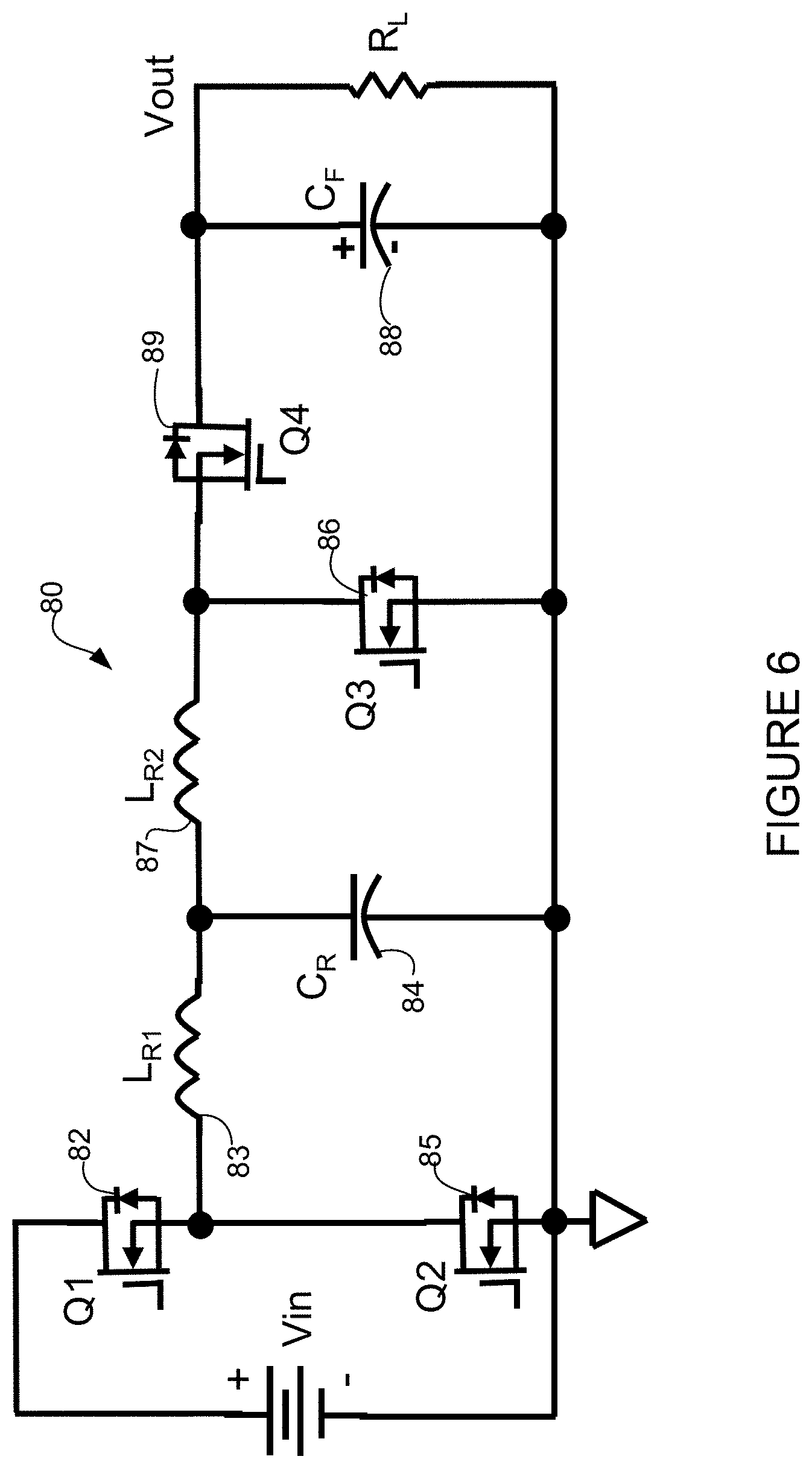
As previously noted, the MRC may also comprise a step-up converter. FIG. 6 illustrates an example of a DC/DC MRC two-switch, two-stage resonant-buck-boost step-down-up power supply that can be used as a voltage step-up or step-down converter, generally indicated at 80. This topology allows simple high efficiency step-up voltage conversion with high voltage input-to-output ratios such as 48:400V, 50:400V, or other suitable ratio (e.g., at least 48:400V). In the example shown in FIG. 6, a first stage includes a first switch 82 (Q1), a first resonant inductor 83 (L.sub.R1), and a resonant capacitor 84 (C.sub.R). The second stage includes a second resonant inductor 87 (L.sub.R2), second switch 86 (Q3) and filter capacitor 88 (C.sub.F). In this example, each stage also includes a synchronous rectifier 85 (Q2), 89 (Q4).
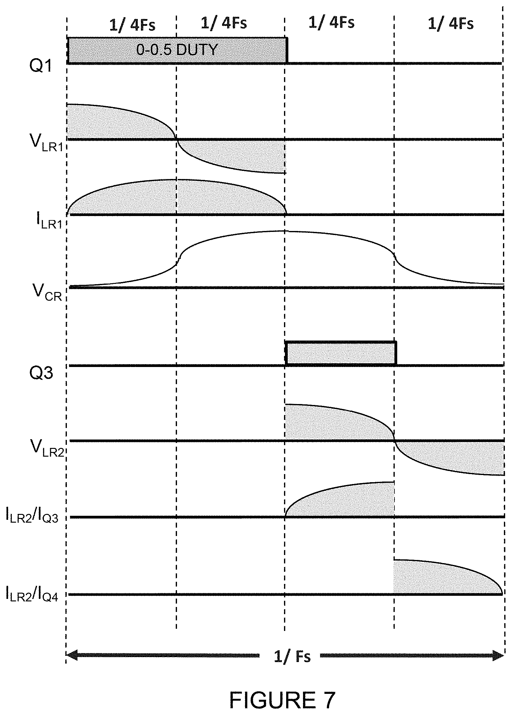
FIG. 7 illustrates operation of the two-stage, two-switch step-up example MRC 80 shown in FIG. 6. The on/off cycles of the switches are shown at Q1 and Q3. Q1 is the duty cycle power charge and Q3 is the power transfer. Q2 and Q4 are synchronous rectifiers, with Q2 a synchronous rectifier only for Q1 duty cycle 0-50% modulation.
Voltage and current between switch Q1 and inductor L.sub.R1 are shown at V.sub.LR1 and I.sub.LR1, respectively. The charge and discharge voltage of C.sub.R is shown at V.sub.CR. Voltage at L.sub.R2 is shown at V.sub.LR2. Current between L.sub.R2 and Q3 is shown at I.sub.LR2/I.sub.Q3 and current between I.sub.LR2 and Q4 is shown at I.sub.LR2/I.sub.Q4.
The following are example power transfer function descriptions for the circuit shown in FIG. 6 and corresponding operation shown in FIG. 7. Vout(Pout*R.sub.L){circumflex over ( )}.sup.0.5 Pout=Pin*Eff=0.5*C.sub.R*V.sub.CR.sup.2*Fs*Eff V.sub.CR=2*Vin*sin(Duty.sub.(0-1)*90.degree.) Wherein: Duty.sub.(0-1)=T.sub.Q1_ON/0.5T.sub.Fs_period C.sub.R=Pout*Duty*Eff/(0.5*V.sub.CR.sup.2*Fs) L.sub.R1=(tR/pi)2/C.sub.R) Wherein: tR=resonant half-sine at 1/2 Fs L.sub.R2=e*(1.5tR*0.5)/di Wherein: e=Vout; and di=Iout/(Duty*0.5 for average) C.sub.F=i*1/Fs/dv Wherein: i=Iout; Fs=switching frequency; and dv=Vp-p ripple
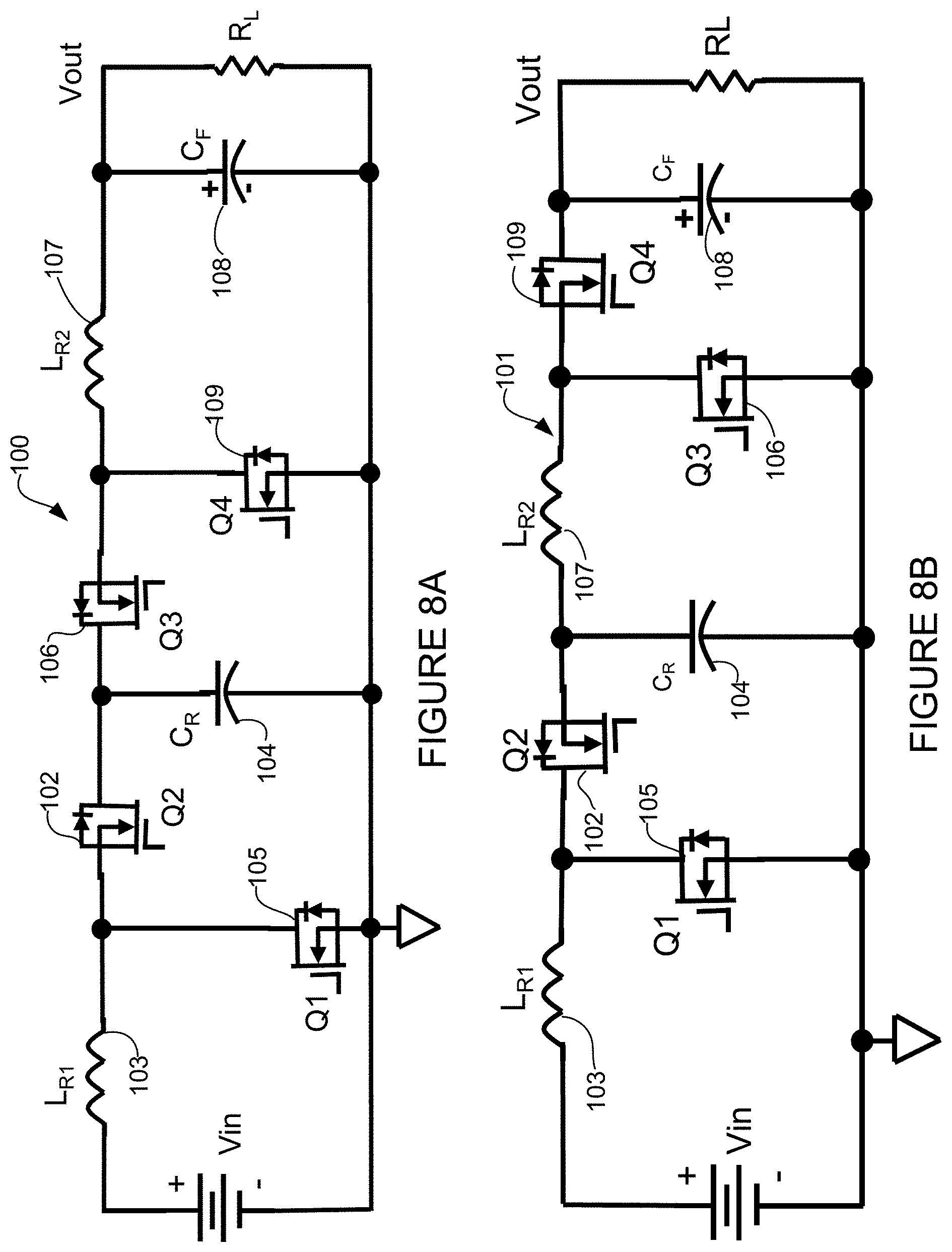
Another example of a DC/DC resonant-boost-buck step-up-down MRC non-isolated (unisolated) voltage converter with two switches and two synchronous rectifiers is shown in FIG. 8A and generally indicated at 100 that can be used as a voltage step-up or a step-down converter. The circuit 100 includes resonant inductors 103 (L.sub.R1), 107 (L.sub.R2), resonant capacitor 104 (C.sub.R), filter capacitor 108 (C.sub.F), switches 105 (Q1) and 106 (Q3), and synchronous rectifiers 102 (Q2), and 109 (Q4). The MRC 100 is configured to provide higher storage charge voltage. An example of an MRC step-up boost-boost, generally indicated at 101 is shown in FIG. 8B. As shown in FIG. 8B, the components in the second stage have been modified to change from a buck to a boost.
In one or more embodiments, a POL converter 110 in accordance with one of the embodiments described herein may be used to replace a conventional IBC (Intermediate-Bus-Converter) and POL converter on a line card or fabric card 112, as shown in FIG. 9. In one example, the POL converter 110 may be used to replace a standard 48:12/10V IBC plus a 12/10V:1V POL converter with a 48:1V POL, while providing high efficiency, small size, low cost package and eliminating a transformer for size and frequency limits. In the example shown in FIG. 9, the POL 110 receives power from a PSU (Power Supply Unit) 114 and provides power to one or more processor (e.g., ASIC (Application Specific Integrated Circuit)), memory, or other chips or devices 116.
It is to be understood that the implementation shown in FIG. 9 is only an example, the POL may be used on any type of board or system type and power supply application, including for example, LED, Laser, battery charger, motor, fan, etc.
The embodiments described herein may be implemented, for example, in Board Mounted Power (BMP) POL power supplies, BMP IBC power supplies, Front End Power (FEP) Power Factor Converter (PFC) power sections, LLC-type resonant power converters, high voltage multipliers, buck, boost, forward, multi-phase stages, or any other suitable applications.
In one example shown in FIG. 10, the MRC topology of FIG. 6 may be incorporated for use in an AC/DC non-isolated PFC (Power Factor Correction) MRC stage to an isolated DC/DC converter, generally indicated at 120. The circuit may comprise, for example, an AC input rectifier to MRC two-stage buck-boost two-switch two-synchronous rectifier example as a step-up converter stage to an isolation DC/DC converter stage. In the example shown in FIG. 10, the circuit includes a PFC stage with a large C.sub.F1 capacitance provides bulk voltage energy storage for line drop-out time protection with output power ride-through time. Also the PFC MRC provides no inrush surge current so no soft-start circuit is needed. Any bulk voltage may be used and switch Q1 and the input bridge rectifier may be replaced with a bridgeless PFC rectifier and first stage switching circuit. The C.sub.R peak voltage may charge to 2 times the maximum peak input line voltage and needs to be lower than the minimum bulk voltage on CF1 to provide good PFC through the input AC waveform. The minimum voltage on C.sub.R needs to be at zero on each switching cycle to provide best PFC though each sine wave half cycle so the L.sub.R1 charge current can follow the rectified input line proportional to the duty cycle of Q1. This may require the second stage Q3 switch to adjust or modulate the duty cycle to less than 90-degrees switching cycle throughout the line rectified sine wave. PFC power supplies may use MRC buck-boost, boost-buck, or boost-boost converters for different applications.
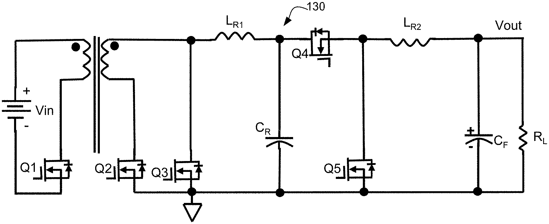
FIGS. 11A, 11B, 12A, and 12B illustrate examples in which the MRC topologies described herein (e.g., MRC topology of FIG. 1) may be used in a DC/DC isolated MRC with a forward converter transformer stage to form a power supply circuit. In one example, a circuit 130 includes an isolated MRC buck-buck step-down-down voltage converter with two switches and three synchronous rectifiers (FIG. 11A). In another example, a circuit 132 forms an isolated MRC resonant buck-boost step-down-up voltage converter with two switches and three synchronous rectifiers (FIG. 11B). FIGS. 12A and 12B illustrate example topologies, generally indicated at 140 and 142, respectively, comprising an isolated MRC with flyback PWM control of the resonant capacitor charge and a synchronous rectifier as the first stage to a resonant-buck or a resonant-boost second stage.
It is to be understood that the circuits shown in FIGS. 10, 11A, 11B, 12A, and 12B are only examples and that the MRC topologies described herein may be incorporated in any other type of circuit or topology to create other types of circuits for implementation in other applications.
The multi-resonant converter (MRC) power supply circuits described herein may be used in any type of power supply application including a network device (e.g., server, router, switch, gateway, controller, edge device, access device, aggregation device, core node, intermediate node, or other network device). The network device may operate in the context of a data communications network including multiple network devices and may communicate over one or more networks.
The network device may be a programmable machine implemented in hardware, software, or any combination thereof. The network device may include one or more processor, memory, and network interface. Memory may be a volatile memory or non-volatile storage, which stores various applications, operating systems, modules, and data for execution and use by the processor. Logic may be encoded in one or more tangible media for execution by the processor. For example, the processor may execute codes stored in a computer-readable medium such as memory. The computer-readable medium may be, for example, electronic (e.g., RAM (random access memory), ROM (read-only memory), EPROM (erasable programmable read-only memory)), magnetic, optical (e.g., CD, DVD), electromagnetic, semiconductor technology, or any other suitable medium. The network interfaces may comprise one or more line cards, fabric cards, service card, router processor card, controller card, or other card, element, or component and the POL converter may be located on one or more the cards. It is to be understood that the network device described herein is only an example and that the embodiments described herein may be implemented on different configurations of network devices.
Although the method and apparatus have been described in accordance with the embodiments shown, one of ordinary skill in the art will readily recognize that there could be variations made to the embodiments without departing from the scope of the invention. Accordingly, it is intended that all matter contained in the above description and shown in the accompanying drawings shall be interpreted as illustrative and not in a limiting sense.
* * * * *
References
-
fischerconnectors.com/us/en/products/fiberoptic
-
strantech.com/products/tfoca-genx-hybrid-2.times.2-fiber-optic-copper-connector
-
qpcfiber.com/product/connectors/e-link-hybrid-connector
-
lumentum.com/sites/default/files/technical-library-items/poweroverfiber-tn-pv-ae_0.pdf
-
voltserver.com
-
pluribusnetworks.com/assets/Pluribus-VirtualWire-PO-50918.pdf
-
wwwjuniper.net/us/en/local/pdf/implementation-guides/8010018-en.pdf
D00000
D00001
D00002
D00003
D00004
D00005
D00006
D00007
D00008
D00009
D00010
D00011
D00012
M00001
XML
uspto.report is an independent third-party trademark research tool that is not affiliated, endorsed, or sponsored by the United States Patent and Trademark Office (USPTO) or any other governmental organization. The information provided by uspto.report is based on publicly available data at the time of writing and is intended for informational purposes only.
While we strive to provide accurate and up-to-date information, we do not guarantee the accuracy, completeness, reliability, or suitability of the information displayed on this site. The use of this site is at your own risk. Any reliance you place on such information is therefore strictly at your own risk.
All official trademark data, including owner information, should be verified by visiting the official USPTO website at www.uspto.gov. This site is not intended to replace professional legal advice and should not be used as a substitute for consulting with a legal professional who is knowledgeable about trademark law.