Display mirror assembly
Lee , et al. A
U.S. patent number 10,739,591 [Application Number 16/030,633] was granted by the patent office on 2020-08-11 for display mirror assembly. This patent grant is currently assigned to GENTEX CORPORATION. The grantee listed for this patent is Gentex Corporation. Invention is credited to Richard T. Fish, Jr., Bradley R. Hamlin, Eric P. Kern, Ethan J. Lee, Danny L. Minikey, Jr..


View All Diagrams
| United States Patent | 10,739,591 |
| Lee , et al. | August 11, 2020 |
| **Please see images for: ( Certificate of Correction ) ** |
Display mirror assembly
Abstract
A display mirror assembly for a vehicle includes a front shield having a first side and a second side. A partially reflective, partially transmissive element is mounted on the first side. A rear shield is disposed behind the front shield. A display module is mounted between the front shield and the rear shield and includes in order from the front shield: a display; an optic block; a heat sink having an edge lit PCB mounted along a top edge thereof; and a PCB. The front shield is secured to at least one component of the display module with a first retaining feature and the rear shield is secured to at least one component of the display module with a second retaining feature. A housing at least partially surrounds the partially reflective, partially transmissive element, the front shield, carrier plate, display module, and rear shield.
| Inventors: | Lee; Ethan J. (Byron Center, MI), Minikey, Jr.; Danny L. (Fenwick, MI), Hamlin; Bradley R. (Allendale, MI), Kern; Eric P. (Holland, MI), Fish, Jr.; Richard T. (Jenison, MI) | ||||||||||
|---|---|---|---|---|---|---|---|---|---|---|---|
| Applicant: |
|
||||||||||
| Assignee: | GENTEX CORPORATION (Zeeland,
MI) |
||||||||||
| Family ID: | 52690704 | ||||||||||
| Appl. No.: | 16/030,633 | ||||||||||
| Filed: | July 9, 2018 |
Prior Publication Data
| Document Identifier | Publication Date | |
|---|---|---|
| US 20180329210 A1 | Nov 15, 2018 | |
Related U.S. Patent Documents
| Application Number | Filing Date | Patent Number | Issue Date | ||
|---|---|---|---|---|---|
| 15437262 | Feb 20, 2017 | 10018843 | |||
| 14494909 | Feb 21, 2017 | 9575315 | |||
| 61881624 | Sep 24, 2013 | ||||
| Current U.S. Class: | 1/1 |
| Current CPC Class: | G02B 27/0149 (20130101); G02F 1/1533 (20130101); B60R 1/12 (20130101); B60R 1/088 (20130101); G02B 2027/0156 (20130101); B60R 2001/1215 (20130101) |
| Current International Class: | G02F 1/153 (20060101); B60R 1/12 (20060101); G02B 27/01 (20060101); G09G 3/19 (20060101); G02F 1/15 (20190101); G02F 1/03 (20060101); B60R 1/08 (20060101) |
| Field of Search: | ;359/265-275,277,245-247,254,242 ;345/49,105,107 ;248/817 ;438/929 |
References Cited [Referenced By]
U.S. Patent Documents
| 2131888 | October 1938 | Harris |
| 2632040 | March 1953 | Rabinow |
| 2827594 | March 1958 | Rabinow |
| 3179845 | April 1965 | Kulwiec |
| 3280701 | October 1966 | Donnelly et al. |
| 3581276 | May 1971 | Newman |
| 3663819 | May 1972 | Hicks et al. |
| 3837129 | September 1974 | Losell |
| 4109235 | August 1978 | Bouthors |
| 4139801 | February 1979 | Linares |
| 4151526 | April 1979 | Hinachi et al. |
| 4214266 | July 1980 | Myers |
| 4236099 | November 1980 | Rosenblum |
| 4257703 | March 1981 | Goodrich |
| 4258979 | March 1981 | Mahin |
| 4277804 | July 1981 | Robison |
| 4286308 | August 1981 | Wolff |
| 4310851 | January 1982 | Pierrat |
| 4357558 | November 1982 | Massoni et al. |
| 4376909 | March 1983 | Tagami et al. |
| 4479173 | October 1984 | Rumpakis |
| 4499451 | February 1985 | Suzuki et al. |
| D283998 | May 1986 | Tanaka |
| 4599544 | July 1986 | Martin |
| 4630904 | December 1986 | Pastore |
| 4638287 | January 1987 | Umebayashi et al. |
| 4645975 | February 1987 | Meitzler et al. |
| 4665321 | May 1987 | Chang et al. |
| 4665430 | May 1987 | Hiroyasu |
| 4692798 | September 1987 | Seko et al. |
| 4716298 | December 1987 | Etoh |
| 4727290 | February 1988 | Smith et al. |
| 4740838 | April 1988 | Mase et al. |
| 4768135 | August 1988 | Kretschmer et al. |
| 4862037 | August 1989 | Farber et al. |
| 4891559 | January 1990 | Matsumoto et al. |
| 4902108 | February 1990 | Byker |
| 4910591 | March 1990 | Petrossian et al. |
| 4930742 | June 1990 | Schofield et al. |
| 4934273 | June 1990 | Endriz |
| 4967319 | October 1990 | Seko |
| 5005213 | April 1991 | Hanson et al. |
| 5008946 | April 1991 | Ando |
| 5027200 | June 1991 | Petrossian et al. |
| 5036437 | July 1991 | Macks |
| 5052163 | October 1991 | Czekala |
| 5066112 | November 1991 | Lynam et al. |
| 5069535 | December 1991 | Baucke et al. |
| 5072154 | December 1991 | Chen |
| 5073012 | December 1991 | Lynam |
| 5076673 | December 1991 | Lynam et al. |
| 5086253 | February 1992 | Lawler |
| 5096287 | March 1992 | Kakinami et al. |
| 5115346 | May 1992 | Lynam |
| 5121200 | June 1992 | Choi et al. |
| 5124549 | June 1992 | Michaels et al. |
| 5128799 | July 1992 | Byker |
| 5151824 | September 1992 | O'Farrell |
| 5158638 | October 1992 | Osanami et al. |
| 5166681 | November 1992 | Bottesch et al. |
| 5182502 | January 1993 | Slotkowski et al. |
| 5187383 | February 1993 | Taccetta et al. |
| 5197562 | March 1993 | Kakinami et al. |
| 5207492 | May 1993 | Roberts |
| 5230400 | July 1993 | Kakinami et al. |
| 5235178 | August 1993 | Hegyi |
| 5243417 | September 1993 | Pollard |
| 5253109 | October 1993 | O'Farrell et al. |
| 5278693 | January 1994 | Theiste |
| 5280380 | January 1994 | Byker |
| 5282077 | January 1994 | Byker |
| 5289321 | February 1994 | Secor |
| 5294376 | March 1994 | Byker |
| 5296924 | March 1994 | Blancard et al. |
| D346356 | April 1994 | Leu |
| 5304980 | April 1994 | Maekawa |
| 5329206 | July 1994 | Slotkowski et al. |
| 5336448 | August 1994 | Byker |
| 5347261 | September 1994 | Adell |
| 5347459 | September 1994 | Greenspan et al. |
| 5355146 | October 1994 | Chiu et al. |
| 5379104 | January 1995 | Takao |
| 5379146 | January 1995 | Defendini |
| 5381309 | January 1995 | Borchardt |
| 5386285 | January 1995 | Asayama |
| 5396054 | March 1995 | Krichever et al. |
| 5402170 | March 1995 | Parulski et al. |
| 5408357 | April 1995 | Beukema |
| 5414461 | May 1995 | Kishi et al. |
| 5416318 | May 1995 | Hegyi |
| 5418610 | May 1995 | Fischer |
| 5421940 | June 1995 | Cornils et al. |
| 5424952 | June 1995 | Asayama |
| 5426294 | June 1995 | Kobayashi et al. |
| 5428464 | June 1995 | Silverbrook |
| 5430450 | July 1995 | Holmes |
| 5434407 | July 1995 | Bauer et al. |
| 5448397 | September 1995 | Tonar |
| 5451822 | September 1995 | Bechtel et al. |
| 5452004 | September 1995 | Roberts |
| 5469298 | November 1995 | Suman et al. |
| 5471515 | November 1995 | Fossum et al. |
| 5475441 | December 1995 | Parulski et al. |
| 5475494 | December 1995 | Nishida et al. |
| 5481268 | January 1996 | Higgins |
| 5483346 | January 1996 | Butzer |
| 5483453 | January 1996 | Uemura et al. |
| 5485155 | January 1996 | Hibino |
| 5485378 | January 1996 | Franke et al. |
| 5488496 | January 1996 | Pine |
| 5508592 | April 1996 | Lapatovich et al. |
| 5515448 | May 1996 | Nishitani |
| 5523811 | June 1996 | Wada et al. |
| 5530421 | June 1996 | Marshall et al. |
| 5535144 | July 1996 | Kise |
| 5537003 | July 1996 | Bechtel et al. |
| 5541590 | July 1996 | Nishio |
| 5541724 | July 1996 | Hoashi |
| 5550677 | August 1996 | Schofield et al. |
| 5554912 | September 1996 | Thayer et al. |
| 5574443 | November 1996 | Hsieh |
| 5574463 | November 1996 | Shirai et al. |
| 5576975 | November 1996 | Sasaki et al. |
| 5587929 | December 1996 | League et al. |
| 5592146 | January 1997 | Kover, Jr. et al. |
| 5602542 | February 1997 | Widmann et al. |
| 5614788 | March 1997 | Mullins et al. |
| 5615023 | March 1997 | Yang |
| 5617085 | April 1997 | Tsutsumi et al. |
| 5621460 | April 1997 | Hatlestad et al. |
| 5634709 | June 1997 | Iwama |
| 5642238 | June 1997 | Sala |
| 5646614 | July 1997 | Abersfelder et al. |
| 5649756 | July 1997 | Adams et al. |
| 5650765 | July 1997 | Park |
| 5660454 | August 1997 | Mori et al. |
| 5666028 | September 1997 | Bechtel et al. |
| 5670935 | September 1997 | Schofield et al. |
| 5679283 | October 1997 | Tonar |
| 5680123 | October 1997 | Lee |
| 5682267 | October 1997 | Tonar |
| 5684473 | November 1997 | Hibino et al. |
| 5689370 | November 1997 | Tonar |
| 5707129 | January 1998 | Kobayashi |
| 5708410 | January 1998 | Blank et al. |
| 5708857 | January 1998 | Ishibashi |
| 5710565 | January 1998 | Shirai et al. |
| 5714751 | February 1998 | Chen |
| 5715093 | February 1998 | Schierbeek et al. |
| 5729194 | March 1998 | Spears et al. |
| 5736816 | April 1998 | Strenke et al. |
| 5742026 | April 1998 | Dickinson |
| 5745050 | April 1998 | Nakagawa |
| 5751211 | May 1998 | Shirai et al. |
| 5751832 | May 1998 | Panter et al. |
| 5754099 | May 1998 | Nishimura et al. |
| 5760828 | June 1998 | Cortes |
| 5764139 | June 1998 | Nojima et al. |
| 5767793 | June 1998 | Agravante et al. |
| 5781105 | July 1998 | Bitar et al. |
| 5786787 | July 1998 | Eriksson et al. |
| 5790298 | August 1998 | Tonar |
| 5793308 | August 1998 | Rosinski et al. |
| 5793420 | August 1998 | Schmidt et al. |
| 5796094 | August 1998 | Schofield et al. |
| 5798727 | August 1998 | Shirai et al. |
| 5803579 | September 1998 | Turnbull |
| 5808778 | September 1998 | Bauer et al. |
| 5811888 | September 1998 | Hsieh |
| 5812321 | September 1998 | Schierbeek et al. |
| 5818625 | October 1998 | Forgette et al. |
| 5825527 | October 1998 | Forgette et al. |
| D400481 | November 1998 | Stephens et al. |
| D401200 | November 1998 | Huang |
| 5837994 | November 1998 | Stam et al. |
| 5841126 | November 1998 | Fossum et al. |
| 5844505 | December 1998 | Van Ryzin |
| 5845000 | December 1998 | Breed et al. |
| 5850146 | December 1998 | Kinoshita et al. |
| 5867214 | February 1999 | Anderson et al. |
| 5877897 | March 1999 | Schofield et al. |
| 5883739 | March 1999 | Ashihara et al. |
| 5888431 | March 1999 | Tonar et al. |
| 5896119 | April 1999 | Evanicky et al. |
| 5904729 | May 1999 | Ruzicka |
| 5905457 | May 1999 | Rashid |
| D410607 | June 1999 | Carter |
| 5912534 | June 1999 | Benedict |
| 5923027 | July 1999 | Stam et al. |
| 5923457 | July 1999 | Byker et al. |
| 5928572 | July 1999 | Tonar et al. |
| 5935613 | August 1999 | Benham et al. |
| 5940011 | August 1999 | Agravante et al. |
| 5940201 | August 1999 | Ash et al. |
| 5942853 | August 1999 | Piscart |
| 5949331 | September 1999 | Schofield et al. |
| 5956012 | September 1999 | Turnbull et al. |
| 5956079 | September 1999 | Ridgley |
| 5956181 | September 1999 | Lin |
| 5959555 | September 1999 | Furuta |
| 5990469 | November 1999 | Bechtel et al. |
| 5998617 | December 1999 | Srinvasa |
| 6002511 | December 1999 | Varaprasad |
| 6008486 | December 1999 | Stam et al. |
| 6009359 | December 1999 | El-Hakim et al. |
| 6018308 | January 2000 | Shirai |
| 6020987 | February 2000 | Baumann |
| 6023040 | February 2000 | Zahavi |
| 6023229 | February 2000 | Bugno et al. |
| 6025872 | February 2000 | Ozaki et al. |
| 6037471 | March 2000 | Srinvasa |
| 6043452 | March 2000 | Bestenlehrer |
| 6046766 | April 2000 | Sakata |
| 6049171 | April 2000 | Stam et al. |
| 6051956 | April 2000 | Nakashimo |
| 6060989 | May 2000 | Gehlot |
| 6061002 | May 2000 | Weber et al. |
| 6062920 | May 2000 | Jordan |
| 6064508 | May 2000 | Forgette et al. |
| 6064509 | May 2000 | Tonar et al. |
| 6067111 | May 2000 | Hahn et al. |
| 6068380 | May 2000 | Lynn et al. |
| 6072391 | June 2000 | Suzuki et al. |
| 6078355 | June 2000 | Zengel |
| 6084700 | July 2000 | Knapp |
| 6097023 | August 2000 | Schofield et al. |
| 6102546 | August 2000 | Carter |
| 6106121 | August 2000 | Buckley et al. |
| 6111498 | August 2000 | Jobes et al. |
| 6111683 | August 2000 | Cammenga |
| 6111684 | August 2000 | Forgette |
| 6115651 | September 2000 | Cruz |
| 6122597 | September 2000 | Saneyoshi et al. |
| 6128576 | October 2000 | Nishimoto et al. |
| 6130421 | October 2000 | Bechtel et al. |
| 6130448 | October 2000 | Bauer et al. |
| 6132072 | October 2000 | Turnbull |
| 6140933 | October 2000 | Bugno et al. |
| 6144158 | November 2000 | Beam |
| 6151065 | November 2000 | Steed et al. |
| 6151539 | November 2000 | Bergholz et al. |
| 6154149 | November 2000 | Tychkowski et al. |
| 6157294 | December 2000 | Urai et al. |
| 6166629 | December 2000 | Andreas |
| 6166698 | December 2000 | Turnbull et al. |
| 6166848 | December 2000 | Cammenga et al. |
| 6167755 | January 2001 | Damson et al. |
| 6170956 | January 2001 | Rumsey et al. |
| 6172600 | January 2001 | Kakinami et al. |
| 6172601 | January 2001 | Wada et al. |
| 6175300 | January 2001 | Kendrick |
| 6181242 | January 2001 | Nguyen |
| 6184781 | February 2001 | Ramakesavan |
| 6185492 | February 2001 | Kagawa et al. |
| 6188505 | February 2001 | Lomprey |
| 6191704 | February 2001 | Takenaga et al. |
| 6193378 | February 2001 | Tonar et al. |
| 6193912 | February 2001 | Theiste |
| 6195194 | February 2001 | Roberts et al. |
| 6200010 | March 2001 | Anders |
| 6218934 | April 2001 | Regan |
| 6222177 | April 2001 | Bechtel |
| 6222447 | April 2001 | Schofield et al. |
| 6224716 | May 2001 | Yoder |
| 6229435 | May 2001 | Knapp |
| 6239898 | May 2001 | Byker |
| 6239899 | May 2001 | Devries et al. |
| 6244716 | June 2001 | Steenwyk |
| 6246507 | June 2001 | Bauer |
| 6247819 | June 2001 | Turnbull |
| 6249214 | June 2001 | Kashiwazaki |
| 6249369 | June 2001 | Theiste et al. |
| 6250766 | June 2001 | Strumolo et al. |
| 6255639 | July 2001 | Stam et al. |
| 6259475 | July 2001 | Ramachandran et al. |
| 6262831 | July 2001 | Bauer |
| 6262832 | July 2001 | Lomprey |
| 6265968 | July 2001 | Betzitza et al. |
| 6268803 | July 2001 | Gunderson et al. |
| 6268950 | July 2001 | Ash |
| 6269308 | July 2001 | Kodaka et al. |
| 6281632 | August 2001 | Stam et al. |
| 6281804 | August 2001 | Haller et al. |
| 6289332 | September 2001 | Menig et al. |
| 6291812 | September 2001 | Bechtel |
| 6300879 | October 2001 | Regan et al. |
| 6304173 | October 2001 | Pala et al. |
| 6313457 | November 2001 | Bauer |
| 6313892 | November 2001 | Gleckman |
| 6317057 | November 2001 | Lee |
| 6317248 | November 2001 | Agrawal et al. |
| 6320612 | November 2001 | Young |
| 6324295 | November 2001 | Avionique et al. |
| D451869 | December 2001 | Knapp et al. |
| 6329925 | December 2001 | Skiver et al. |
| 6330511 | December 2001 | Ogura et al. |
| 6335548 | January 2002 | Roberts |
| 6335680 | January 2002 | Matsuoka |
| 6344805 | February 2002 | Yasui et al. |
| 6348858 | February 2002 | Weis et al. |
| 6349782 | February 2002 | Sekiya et al. |
| 6356206 | March 2002 | Takenaga et al. |
| 6356376 | March 2002 | Tonar et al. |
| 6357883 | March 2002 | Strumolo et al. |
| 6359274 | March 2002 | Nixon |
| 6363326 | March 2002 | Scully |
| 6369701 | April 2002 | Yoshida et al. |
| 6379013 | April 2002 | Bechtel et al. |
| 6392783 | May 2002 | Lomprey |
| 6396040 | May 2002 | Hill |
| 6396397 | May 2002 | Bos et al. |
| 6402328 | June 2002 | Bechtel |
| 6403942 | June 2002 | Stam |
| 6407468 | June 2002 | LeVesque et al. |
| 6407847 | June 2002 | Poll et al. |
| 6408247 | June 2002 | Ichikawa et al. |
| 6412959 | July 2002 | Tseng |
| 6415230 | July 2002 | Maruko et al. |
| 6420800 | July 2002 | Levesque |
| 6421081 | July 2002 | Markus |
| 6424272 | July 2002 | Gutta et al. |
| 6424273 | July 2002 | Gutta et al. |
| 6424892 | July 2002 | Matsuoka |
| 6426485 | July 2002 | Buljajewski |
| 6428172 | August 2002 | Hutzel et al. |
| 6429594 | August 2002 | Stam |
| 6433680 | August 2002 | Ho |
| 6437688 | August 2002 | Kobayashi |
| 6438491 | August 2002 | Farmer |
| 6441872 | August 2002 | Ho |
| 6441943 | August 2002 | Roberts |
| 6442465 | August 2002 | Breed et al. |
| 6443585 | September 2002 | Saccomanno |
| 6443602 | September 2002 | Tanabe et al. |
| 6447128 | September 2002 | Lang et al. |
| 6447130 | September 2002 | Chu |
| 6452533 | September 2002 | Yamabuchi et al. |
| 6463369 | October 2002 | Sadano et al. |
| 6465962 | October 2002 | Fu et al. |
| 6465963 | October 2002 | Turnbull |
| 6466701 | October 2002 | Ejiri et al. |
| 6469739 | October 2002 | Bechtel et al. |
| 6471362 | October 2002 | Carter |
| 6472977 | October 2002 | Pochmuller |
| 6473001 | October 2002 | Blum |
| 6476731 | November 2002 | Miki et al. |
| 6476855 | November 2002 | Yamamoto |
| 6483429 | November 2002 | Yasui et al. |
| 6483438 | November 2002 | DeLine et al. |
| 6487500 | November 2002 | Lemelson et al. |
| 6491416 | December 2002 | Strazzanti |
| 6498620 | December 2002 | Schofield et al. |
| 6501387 | December 2002 | Skiver et al. |
| 6504142 | January 2003 | Nixon |
| 6507779 | January 2003 | Breed et al. |
| 6512624 | January 2003 | Tonar |
| 6515581 | February 2003 | Ho |
| 6515597 | February 2003 | Wada et al. |
| 6520667 | February 2003 | Mousseau |
| 6521916 | February 2003 | Roberts |
| 6522969 | February 2003 | Kannonji |
| 6523976 | February 2003 | Turnbull |
| D471847 | March 2003 | Rumsey et al. |
| 6535126 | March 2003 | Lin et al. |
| 6542085 | April 2003 | Yang |
| 6542182 | April 2003 | Chutorash |
| 6545598 | April 2003 | de Villeroche |
| 6545794 | April 2003 | Ash |
| 6550943 | April 2003 | Strazzanti |
| 6553130 | April 2003 | Lemelson et al. |
| 6558026 | May 2003 | Strazzanti |
| 6559761 | May 2003 | Miller et al. |
| 6572233 | June 2003 | Northman et al. |
| 6580373 | June 2003 | Ohashi |
| 6581007 | June 2003 | Hasegawa et al. |
| 6583730 | June 2003 | Lang et al. |
| 6575643 | July 2003 | Takashashi |
| 6587573 | July 2003 | Stam et al. |
| 6591192 | July 2003 | Okamura et al. |
| 6594583 | July 2003 | Ogura et al. |
| 6594614 | July 2003 | Studt et al. |
| 6606183 | August 2003 | Ikai et al. |
| 6611202 | August 2003 | Schofield et al. |
| 6611227 | August 2003 | Nebiyeloul-Kifle |
| 6611610 | August 2003 | Stam et al. |
| 6611759 | August 2003 | Brosche |
| 6612708 | September 2003 | Chu |
| 6614387 | September 2003 | Deadman |
| 6614579 | September 2003 | Roberts et al. |
| 6616764 | September 2003 | Kramer et al. |
| 6617564 | September 2003 | Ockerse et al. |
| 6618672 | September 2003 | Sasaki et al. |
| 6630888 | October 2003 | Lang et al. |
| 6631316 | October 2003 | Stam et al. |
| 6635194 | October 2003 | Kloeppner |
| 6636258 | October 2003 | Strumolo |
| 6642840 | November 2003 | Lang et al. |
| 6642851 | November 2003 | DeLine et al. |
| 6648477 | November 2003 | Hutzel et al. |
| 6650457 | November 2003 | Busscher et al. |
| 6657767 | December 2003 | Bonardi |
| 6665592 | December 2003 | Kodama |
| 6670207 | December 2003 | Roberts |
| 6670910 | December 2003 | Delcheccolo et al. |
| 6674370 | January 2004 | Rodewald et al. |
| 6675075 | January 2004 | Engelsberg et al. |
| 6677986 | January 2004 | Pochmuller |
| 6683539 | January 2004 | Trajkovic et al. |
| 6683969 | January 2004 | Nishigaki et al. |
| 6690268 | February 2004 | Schofield et al. |
| 6690413 | February 2004 | Moore |
| 6693517 | February 2004 | McCarty et al. |
| 6693518 | February 2004 | Kumata |
| 6693519 | February 2004 | Keirstead |
| 6693524 | February 2004 | Payne |
| 6700692 | March 2004 | Tonar |
| 6717610 | April 2004 | Bos et al. |
| 6727808 | April 2004 | Uselmann et al. |
| 6727844 | April 2004 | Zimmermann et al. |
| 6731332 | May 2004 | Yasui et al. |
| 6734807 | May 2004 | King |
| 6737964 | May 2004 | Samman et al. |
| 6738088 | May 2004 | Uskolovsky et al. |
| 6744353 | June 2004 | Sjonell |
| 6746122 | June 2004 | Knox |
| D493131 | July 2004 | Lawlor et al. |
| D493394 | July 2004 | Lawlor et al. |
| 6768566 | July 2004 | Walker |
| 6772057 | August 2004 | Breed et al. |
| 6774988 | August 2004 | Stam et al. |
| 6781738 | August 2004 | Kikuchi et al. |
| 6816145 | November 2004 | Evanicky |
| 6816297 | November 2004 | Tonar |
| D499678 | December 2004 | Bradley |
| 6846098 | January 2005 | Bourdelais et al. |
| 6847487 | January 2005 | Burgner |
| 6853413 | February 2005 | Larson |
| 6861809 | March 2005 | Stam |
| 6870656 | March 2005 | Tonar et al. |
| 6902284 | June 2005 | Hutzel et al. |
| 6902307 | June 2005 | Strazzanti |
| 6912001 | June 2005 | Okamoto et al. |
| 6913375 | July 2005 | Strazzanti |
| 6923080 | August 2005 | Dobler et al. |
| 6930737 | August 2005 | Weindorf et al. |
| 6934080 | August 2005 | Saccomanno et al. |
| 6946978 | September 2005 | Schofield |
| 6958495 | October 2005 | Nishijima et al. |
| 6968273 | November 2005 | Ockerse |
| 7012543 | March 2006 | DeLine et al. |
| 7038577 | May 2006 | Pawlicki et al. |
| 7042616 | May 2006 | Tonar et al. |
| 7046448 | May 2006 | Burgner |
| 7064882 | June 2006 | Tonar |
| 7175291 | February 2007 | Li |
| 7255465 | August 2007 | DeLine et al. |
| 7262406 | August 2007 | Heslin et al. |
| 7265342 | September 2007 | Heslin et al. |
| D553061 | October 2007 | Schmidt et al. |
| 7285903 | October 2007 | Cull et al. |
| 7287868 | October 2007 | Carter |
| 7292208 | November 2007 | Park et al. |
| 7311428 | December 2007 | DeLine et al. |
| 7321112 | January 2008 | Stam et al. |
| 7324261 | January 2008 | Tonar et al. |
| 7342707 | March 2008 | Roberts |
| 7349143 | March 2008 | Tonar et al. |
| 7360932 | April 2008 | Uken et al. |
| 7417221 | August 2008 | Creswick et al. |
| 7417717 | August 2008 | Pack |
| 7446650 | November 2008 | Schofield et al. |
| 7467883 | December 2008 | DeLine et al. |
| 7468651 | December 2008 | DeLine et al. |
| 7505047 | March 2009 | Yoshimura |
| 7533998 | May 2009 | Schofield et al. |
| 7548291 | June 2009 | Lee et al. |
| 7565006 | July 2009 | Stam et al. |
| 7567291 | July 2009 | Bechtel et al. |
| 7579940 | August 2009 | Schofield et al. |
| 7592563 | September 2009 | Wissenbach |
| 7619508 | November 2009 | Lynam et al. |
| 7626749 | December 2009 | Baur et al. |
| 7653215 | January 2010 | Stam |
| 7658521 | February 2010 | DeLine et al. |
| 7663798 | February 2010 | Tonar |
| 7683326 | March 2010 | Stam et al. |
| 7688495 | March 2010 | Tonar et al. |
| 7706046 | April 2010 | Bauer et al. |
| 7711479 | May 2010 | Taylor et al. |
| 7719408 | May 2010 | Deward et al. |
| 7720580 | May 2010 | Higgins-Luthman |
| 7746534 | June 2010 | Tonar et al. |
| 7815326 | October 2010 | Blank et al. |
| 7817020 | October 2010 | Turnbull et al. |
| 7821696 | October 2010 | Tonar et al. |
| 7830583 | November 2010 | Neuman et al. |
| 7864399 | January 2011 | McCabe et al. |
| 7877175 | January 2011 | Higgins-Luthman |
| 7881496 | February 2011 | Camilleri et al. |
| 7881839 | February 2011 | Stam et al. |
| 7888629 | February 2011 | Heslin et al. |
| 7914188 | March 2011 | DeLine et al. |
| 7972045 | July 2011 | Schofield |
| 7978393 | July 2011 | Tonar et al. |
| 7994471 | August 2011 | Heslin et al. |
| 8031225 | October 2011 | Watanabe et al. |
| 8035881 | October 2011 | Luten et al. |
| 8045760 | October 2011 | Stam et al. |
| 8059235 | November 2011 | Utsumi et al. |
| 8063753 | November 2011 | DeLine et al. |
| 8090153 | January 2012 | Schofield et al. |
| 8095310 | January 2012 | Taylor et al. |
| 8100568 | January 2012 | DeLine et al. |
| 8116929 | February 2012 | Higgins-Luthman |
| 8120652 | February 2012 | Bechtel et al. |
| 8142059 | March 2012 | Higgins-Luthman et al. |
| 8162518 | April 2012 | Schofield |
| 8194133 | June 2012 | DeWind et al. |
| 8201800 | June 2012 | Filipiak |
| 8203433 | June 2012 | Deuber et al. |
| 8217830 | July 2012 | Lynam |
| 8222588 | July 2012 | Schofield et al. |
| 8237909 | August 2012 | Ostreko et al. |
| 8258433 | September 2012 | Byers et al. |
| 8282226 | October 2012 | Blank et al. |
| 8325028 | December 2012 | Schofield et al. |
| 8339526 | December 2012 | Minikey, Jr. et al. |
| 8475018 | July 2013 | Belcher et al. |
| 8482683 | July 2013 | Hwang et al. |
| 8520069 | August 2013 | Haler |
| 8559092 | October 2013 | Bugno et al. |
| 8564662 | October 2013 | Busch et al. |
| 8779910 | July 2014 | DeLine et al. |
| D729714 | May 2015 | Roth |
| 9134585 | September 2015 | Tonar et al. |
| D746744 | January 2016 | Sloterbeek et al. |
| 9319639 | April 2016 | Englander et al. |
| D755097 | May 2016 | Lin |
| 10071689 | September 2018 | VanderPloeg et al. |
| 2001/0019356 | September 2001 | Takeda et al. |
| 2001/0022616 | September 2001 | Rademacher et al. |
| 2001/0026316 | October 2001 | Senatore |
| 2001/0045981 | November 2001 | Gloger et al. |
| 2002/0040962 | April 2002 | Schofield et al. |
| 2002/0044065 | April 2002 | Quist et al. |
| 2002/0080021 | June 2002 | Skiver et al. |
| 2002/0191127 | December 2002 | Roberts et al. |
| 2003/0002165 | January 2003 | Mathias et al. |
| 2003/0007261 | January 2003 | Hutzel et al. |
| 2003/0016125 | January 2003 | Lang et al. |
| 2003/0016287 | January 2003 | Nakayama et al. |
| 2003/0025596 | February 2003 | Lang et al. |
| 2003/0025597 | February 2003 | Schofield |
| 2003/0030546 | February 2003 | Tseng |
| 2003/0030551 | February 2003 | Ho |
| 2003/0030724 | February 2003 | Okamoto |
| 2003/0035050 | February 2003 | Mizusawa |
| 2003/0043269 | March 2003 | Park |
| 2003/0052969 | March 2003 | Satoh et al. |
| 2003/0058338 | March 2003 | Kawauchi et al. |
| 2003/0067383 | April 2003 | Yang |
| 2003/0076415 | April 2003 | Strumolo |
| 2003/0080877 | May 2003 | Takagi et al. |
| 2003/0085806 | May 2003 | Samman et al. |
| 2003/0088361 | May 2003 | Sekiguchi |
| 2003/0090568 | May 2003 | Pico |
| 2003/0090569 | May 2003 | Poechmueller |
| 2003/0090570 | May 2003 | Takagi et al. |
| 2003/0098908 | May 2003 | Misaiji et al. |
| 2003/0103141 | June 2003 | Bechtel et al. |
| 2003/0103142 | June 2003 | Hitomi et al. |
| 2003/0117522 | June 2003 | Okada |
| 2003/0122929 | July 2003 | Minaudo et al. |
| 2003/0122930 | July 2003 | Schofield et al. |
| 2003/0133014 | July 2003 | Mendoza |
| 2003/0137586 | July 2003 | Lewellen |
| 2003/0141965 | July 2003 | Gunderson et al. |
| 2003/0146831 | August 2003 | Berberich et al. |
| 2003/0169158 | September 2003 | Paul, Jr. |
| 2003/0179293 | September 2003 | Oizumi |
| 2003/0202096 | October 2003 | Kim |
| 2003/0202357 | October 2003 | Strazzanti |
| 2003/0214576 | November 2003 | Koga |
| 2003/0214584 | November 2003 | Ross, Jr. |
| 2003/0214733 | November 2003 | Fujikawa et al. |
| 2003/0222793 | December 2003 | Tanaka et al. |
| 2003/0222983 | December 2003 | Nobori et al. |
| 2003/0227546 | December 2003 | Hilborn et al. |
| 2004/0004541 | January 2004 | Hong |
| 2004/0027695 | January 2004 | Lin |
| 2004/0032321 | February 2004 | McMahon et al. |
| 2004/0036768 | February 2004 | Green |
| 2004/0075603 | February 2004 | Kodama |
| 2004/0051634 | March 2004 | Schofield et al. |
| 2004/0056955 | March 2004 | Berberich et al. |
| 2004/0057131 | March 2004 | Hutzel et al. |
| 2004/0064241 | April 2004 | Sekiguchi |
| 2004/0066285 | April 2004 | Sekiguchi |
| 2004/0080404 | April 2004 | White |
| 2004/0080431 | April 2004 | White |
| 2004/0085196 | May 2004 | Miller et al. |
| 2004/0090314 | May 2004 | Iwamoto |
| 2004/0090317 | May 2004 | Rothkop |
| 2004/0096082 | May 2004 | Nakai et al. |
| 2004/0098196 | May 2004 | Sekiguchi |
| 2004/0107030 | June 2004 | Nishira et al. |
| 2004/0107617 | June 2004 | Shoen et al. |
| 2004/0109060 | June 2004 | Ishii |
| 2004/0114039 | June 2004 | Ishikura |
| 2004/0119668 | June 2004 | Homma et al. |
| 2004/0125905 | July 2004 | Vlasenko et al. |
| 2004/0196577 | October 2004 | Carter et al. |
| 2004/0202001 | October 2004 | Roberts et al. |
| 2005/0099693 | May 2005 | Schofield et al. |
| 2005/0140855 | June 2005 | Utsumi |
| 2005/0237440 | October 2005 | Sugimura et al. |
| 2006/0007550 | January 2006 | Tonar et al. |
| 2006/0115759 | June 2006 | Kim et al. |
| 2006/0139953 | June 2006 | Chou et al. |
| 2006/0158899 | July 2006 | Ayabe et al. |
| 2007/0146481 | June 2007 | Chen et al. |
| 2007/0171037 | July 2007 | Schofield et al. |
| 2008/0030836 | February 2008 | Tonar et al. |
| 2008/0068520 | March 2008 | Minikey, Jr. et al. |
| 2008/0192132 | August 2008 | Bechtel et al. |
| 2008/0247192 | October 2008 | Hoshi et al. |
| 2008/0294315 | November 2008 | Breed |
| 2008/0302657 | December 2008 | Luten et al. |
| 2009/0015736 | January 2009 | Weller et al. |
| 2009/0141516 | June 2009 | Wu et al. |
| 2009/0296190 | December 2009 | Anderson et al. |
| 2010/0110553 | May 2010 | Anderson et al. |
| 2010/0194890 | August 2010 | Weller et al. |
| 2010/0201816 | August 2010 | Lee et al. |
| 2010/0201896 | August 2010 | Ostreko et al. |
| 2010/0277786 | November 2010 | Anderson et al. |
| 2010/0289995 | November 2010 | Hwang et al. |
| 2010/0328463 | December 2010 | Haler |
| 2011/0168687 | July 2011 | Door |
| 2011/0176323 | July 2011 | Skiver et al. |
| 2011/0181727 | July 2011 | Weller et al. |
| 2011/0255297 | October 2011 | Belcher et al. |
| 2011/0317015 | December 2011 | Seto et al. |
| 2012/0038964 | February 2012 | De Wind et al. |
| 2012/0069444 | March 2012 | Campbell et al. |
| 2012/0182242 | July 2012 | Lindahl et al. |
| 2012/0229882 | September 2012 | Fish, Jr. et al. |
| 2012/0236388 | September 2012 | De Wind et al. |
| 2013/0028473 | January 2013 | Hilldore et al. |
| 2013/0170013 | July 2013 | Tonar et al. |
| 2013/0279014 | October 2013 | Fish, Jr. et al. |
| 2014/0022390 | January 2014 | Blank et al. |
| 2014/0043479 | February 2014 | Busch et al. |
| 2014/0192431 | July 2014 | Sloterbeek et al. |
| 2014/0347488 | November 2014 | Tazaki et al. |
| 2015/0055223 | February 2015 | Fish, Jr. et al. |
| 2015/0085337 | March 2015 | Lee et al. |
| 102010064082 | Jun 2012 | DE | |||
| 0513476 | Nov 1992 | EP | |||
| 434453 | Apr 1997 | EP | |||
| 0899157 | Oct 2004 | EP | |||
| 2393691 | May 2014 | EP | |||
| 2789505 | Oct 2014 | EP | |||
| 2845921 | Mar 2015 | EP | |||
| 2338363 | Dec 1999 | GB | |||
| H07242147 | Sep 1995 | JP | |||
| H07267002 | Oct 1995 | JP | |||
| H1178693 | Mar 1999 | JP | |||
| 2002096685 | Apr 2002 | JP | |||
| 2002120649 | Apr 2002 | JP | |||
| 2002200936 | Jul 2002 | JP | |||
| 2005102206 | Apr 2005 | JP | |||
| 2005148119 | Jun 2005 | JP | |||
| 2005327600 | Nov 2005 | JP | |||
| 2008139819 | Jun 2008 | JP | |||
| 2009158451 | Jul 2009 | JP | |||
| 2009542505 | Dec 2009 | JP | |||
| 2010173460 | Aug 2010 | JP | |||
| 2011037436 | Feb 2011 | JP | |||
| 2011076834 | Apr 2011 | JP | |||
| 2013037334 | Feb 2013 | JP | |||
| 2013244753 | Dec 2013 | JP | |||
| 2013246324 | Dec 2013 | JP | |||
| 0138008 | Apr 1999 | KR | |||
| 20100123433 | Nov 2010 | KR | |||
| 9621581 | Jul 1996 | WO | |||
| 2007006104 | Jan 2007 | WO | |||
| 2007103573 | Sep 2007 | WO | |||
| 2010090964 | Aug 2010 | WO | |||
| 2011044312 | Apr 2011 | WO | |||
| 2013084622 | Jun 2013 | WO | |||
| 2013162985 | Oct 2013 | WO | |||
Other References
|
Palalau et al., "FPD Evaluation for Automotive Application," Proceedings of the Vehicle Display Symposium, Nov. 2, 1995, pp. 97-103, Society for Information Display, Detroit Chapter, Santa Ana, CA. cited by applicant . Adler, "A New Automotive AMLCD Module," Proceedings of the Vehicle Display Symposium, Nov. 2, 1995, pp. 67-71, Society for Information Display, Detroit Chapter, Santa Ana, CA. cited by applicant . Sayer, et al., "In-Vehicle Displays for Crash Avoidance and Navigation Systems," Proceedings of the Vehicle Display Symposium, Sep. 18, 1996, pp. 39-42, Society for Information Display, Detroit Chapter, Santa Ana, CA. cited by applicant . Knoll, et al., "Application of Graphic Displays in Automobiles," SID 87 Digest, 1987, pp. 41-44, 5A.2. cited by applicant . Terada, et al., "Development of Central Information Display of Automotive Application," SID 89 Digest, 1989, pp. 192-195, Society for Information Display, Detroit Center, Santa Ana, CA. cited by applicant . Thomsen, et al., "AMLCD Design Considerations for Avionics and Vetronics Applications," Proceedings of the 5th Annual Flat Panel Display Strategic and Technical Symposium, Sep. 9-10, 1998, pp. 139-145, Society for Information Display, Metropolitan Detroit Chapter, CA. cited by applicant . Knoll, et al., "Conception of an Integrated Driver Information System," SID International Symposium Digest of Technical Papers, 1990, pp. 126-129, Society for Information Display, Detroit Center, Santa Ana, CA. cited by applicant . Vincen, "An Analysis of Direct-View FPDs for Automotive Multi-Media Applications," Proceedings of the 6th Annual Strategic and Technical Symposium "Vehicular Applications of Displays and Microsensors," Sep. 22-23, 1999, pp. 39-46, Society for Information Display, Metropolitan Detroit Chapter, San Jose, CA. cited by applicant . Zuk, et al., "Flat Panel Display Applications in Agriculture Equipment," Proceedings of the 5th Annual Flat Panel Display Strategic and Technical Symposium, Sep. 9-10, 1998, pp. 125-130, Society for Information Display, Metropolitan Detroit Chapter, CA. cited by applicant . Vijan, et al., "A 1.7-Mpixel Full-Color Diode Driven AM-LCD," SID International Symposium, 1990, pp. 530-533, Society for Information Display, Playa del Rey, CA. cited by applicant . Vincen, "The Automotive Challenge to Active Matrix LCD Technology," Proceedings of the Vehicle Display Symposium, 1996, pp. 17-21, Society for Information Display, Detroit Center, Santa Ana, CA. cited by applicant . Corsi, et al., "Reconfigurable Displays Used as Primary Automotive Instrumentation," SAE Technical Paper Series, 1989, pp. 13-18, Society of Automotive Engineers, Inc., Warrendale, PA. cited by applicant . Schumacher, "Automotive Display Trends," SID 96 Digest, 1997, pp. 1-6, Delco Electronics Corp., Kokomo, IN. cited by applicant . Knoll, "The Use of Displays in Automotive Applications," Journal of the SID 5/3 1997, pp. 165-172, 315-316, Stuttgart, Germany. cited by applicant . Donofrio, "Looking Beyond the Dashboard," SID 2002, pp. 30-34, Ann Arbor, MI. cited by applicant . Stone, "Automotive Display Specification," Proceedings of the Vehicle Display Symposium, 1995, pp. 93-96, Society or Information Display, Detroit Center, Santa Ana, CA. cited by applicant. |
Primary Examiner: Pinkney; Dawayne
Attorney, Agent or Firm: Price Heneveld LLP Johnson; Bradley D.
Parent Case Text
CROSS-REFERENCE TO RELATED APPLICATIONS
This application is a continuation of and claims priority to U.S. patent application Ser. No. 15/437,262, filed on Feb. 20, 2017, entitled "DISPLAY MIRROR ASSEMBLY," now U.S. Pat. No. 10,018,843, which is a continuation of and claims priority to U.S. patent application Ser. No. 14/494,909, filed on Sep. 24, 2014, entitled "DISPLAY MIRROR ASSEMBLY," now U.S. Pat. No. 9,575,315, which claims the benefit under 35 U.S.C. .sctn. 119(e) of U.S. Provisional Patent Application No. 61/881,624, filed on Sep. 24, 2013, entitled "DISPLAY MIRROR ASSEMBLY," the entire disclosures of which are hereby incorporated herein by reference.
Claims
What is claimed is:
1. A rearview system for a vehicle, the rearview system comprising: an electro-optic element including: a partially reflective, partially transmissive front substrate having a rounded peripheral edge, the front substrate defining a first surface and a second surface; a rear substrate defining a third surface and a fourth surface; and an electro-optic medium disposed between the front substrate and the rear substrate; a control circuit configured to control and power the electro-optic element; a mounting member operably coupled to said vehicle and to the electro-optic element, the mounting member routing wiring from said vehicle to the electro-optic element; an imager configured to capture image data outside said vehicle, wherein a signal representative of received light is communicated from the imager to the control circuit, wherein the captured image data is evaluated by the control circuit to determine likely glare on the electro-optic element; and a bi-modal switch operably coupled with the electro-optic element and configured to rotate the electro-optic element between on-axis and off-axis positions and also activate or deactivate a display module.
2. The rearview system of claim 1, wherein the imager is disposed on a rear portion of said vehicle.
3. The rearview system of claim 1, further comprising: a display adjacent the rear substrate, the display including one of an LCD, LED, OLED, plasma, and DLP display element.
4. The rearview system of claim 1, wherein an outer perimeter of the electro-optic element is frameless.
5. The rearview system of claim 1, wherein the mounting member includes a ball section disposed adjacent the rear substrate.
6. The rearview system of claim 4, wherein the ball section includes a mounting plate proximate the rear substrate.
7. A rearview system for a vehicle, the rearview system comprising: an electro-optic element including: a front substrate; a rear substrate; and an electro-optic medium disposed therebetween; a mounting member operably coupled to said vehicle and to the electro-optic element, the mounting member routing wiring to the electro-optic element; an imager disposed on said vehicle, wherein a signal representative of received light is communicated from the imager through the mounting member to the electro-optic element of said rearview assembly to change an opacity of the electro-optic element; and a bi-modal switch disposed on a bottom side of the electro-optic element and configured to move the electro-optic element between on-axis and off-axis positions and also activate and deactivate a display module of said rearview system.
8. The rearview system of claim 7, wherein the imager is disposed on a rear portion of said vehicle.
9. The rearview system of claim 7, further comprising: a display adjacent the rear substrate, the display including one of an LCD, LED, OLED, plasma, and DLP display element.
10. The rearview system of claim 7, wherein an outer perimeter of the electro-optic element is frameless.
11. The rearview system of claim 7, wherein the mounting member includes a ball section disposed adjacent the rear substrate.
12. The rearview system of claim 11, wherein the ball section includes a mounting plate proximate the rear substrate.
13. A rearview system for a vehicle, the rearview system comprising: a display mirror assembly including a partially reflective, partially transmissive element, the partially reflective, partially transmissive element comprising: a front substrate; a rear substrate; and an electro-optic medium disposed therebetween; a mounting member operably coupled to said vehicle and to the partially reflective, partially transmissive element, the mounting member routing wiring to the partially reflective, partially transmissive element; an imager disposed on said vehicle, wherein a signal representative of received light is communicated from the imager through the mounting member to the partially reflective, partially transmissive element of said rearview assembly to change an opacity of the partially reflective, partially transmissive element; a display module disposed adjacent to the rear substrate, the display module configured to display image data captured by the imager; and a bi-modal switch that activates and deactivates the display module and rotates the display mirror assembly relative to the mounting member.
14. The rearview system of claim 13, wherein the display module includes one of an LCD, LED, OLED, plasma, and DLP display element.
15. The rearview system of claim 13, wherein the imager is disposed on a rear portion of said vehicle.
16. The rearview system of claim 13, wherein an outer perimeter of the partially reflective, partially transmissive element is frameless.
17. The rearview system of claim 13, wherein the mounting member includes a ball section disposed adjacent the rear substrate.
18. The rearview system of claim 17, wherein the ball section includes a mounting plate proximate the rear substrate.
Description
BACKGROUND OF THE DISCLOSURE
The present disclosure generally relates to a rearview device system, and more particularly, a display mirror assembly having a partially reflective, partially transmissive element and a display behind the reflective element.
SUMMARY OF THE DISCLOSURE
At least one aspect of the disclosure includes a display mirror assembly for a vehicle having a front shield including a first side and a second side. A partially reflective, partially transmissive element is mounted on the first side. A rear shield is disposed behind the front shield. A carrier plate is disposed between the front shield and the rear shield. A display module is mounted between the front shield and the rear shield and includes in order from the front shield: a display; an optic block; a heat sink having an edge lit PCB mounted along a top edge thereof; and a PCB. The front shield is secured to at least one component of the display module with a first retaining feature and the rear shield is secured to at least one component of the display module with a second retaining feature. A housing at least partially surrounds the front shield, display module, and rear shield.
At least one aspect of the disclosure includes an RF shield for a display mirror having a first metallic shield member with RF shielding properties. The first metallic shield member forms a carrier plate having structural features configured to support a display module. A second metallic shield member includes RF shielding properties. The first metallic shield member and the second metallic shield member each have retaining features to operatively engage the display module disposed between the first metallic shield member and the second metallic shield member.
At least one aspect of the disclosure includes a method of manufacturing a display mirror assembly for a vehicle. A partially reflective, partially transmissive element is affixed to a front side of a front shield. A display module is positioned on a rear side of the front shield and the front shield is operably secured to the display module. A rear shield is positioned on a rear side of the display module the rear shield is operably secured to the display module. The front shield, the display module, and the rear shield are operably secured between a glass element and a rear housing in a carrier plate free configuration.
At least one aspect of the disclosure includes a display mirror assembly for a vehicle having a housing. A mirror assembly is operably coupled with the housing. A display module is mounted to the housing. A display switch is operable between an on state and an off state corresponding to activation and deactivation, respectively, of the display module. The display module includes a printed circuit board (PCB). A bi-modal switch is rotatably coupled with the housing. The bi-modal switch is adjustable to a first position that rotates the mirror assembly to optimize visibility of an image and which simultaneously moves the display switch to the off state. The bi-modal switch is also adjustable to a second position that rotates the mirror assembly to a position that is not optimal for visibility of an image and which simultaneously moves the display switch to the on state.
At least one aspect of the present disclosure includes a bi-modal switch that is operably connected to the display module, the bi-modal switch extends outwards with respect to the housing. The bi-modal switch is configured to actuate to and from at least a first position and a second position that activate or deactivate the display module and pivot the pitch of a mirror element viewable by an occupant approximately between 2 degrees and 7 degrees.
These and other features, advantages, and objects of the present disclosure will be further understood and appreciated by those skilled in the art by reference to the following specification, claims, and appended drawings.
BRIEF DESCRIPTION OF THE DRAWINGS
FIG. 1 is a top front perspective view of a display mirror assembly for a vehicle;
FIG. 2 is a bottom front perspective view of the display mirror assembly of FIG. 1;
FIG. 3 is a side elevation view of the display mirror assembly of FIG. 1;
FIG. 4 is a partially exploded top perspective view of the display mirror assembly of FIG. 1;
FIG. 5 is a partially exploded top perspective view of the display mirror assembly of FIG. 1;
FIG. 6 is an exploded top perspective view of the display mirror assembly of FIG. 1
FIG. 7A is a isometric front perspective view of a display mirror assembly for a vehicle with a bi-modal switch;
FIG. 7B is a front perspective view of the display mirror assembly of FIG. 7A;
FIG. 7C is a side elevation view of the display mirror assembly of FIG. 7A;
FIG. 7D is a side elevation view of the display mirror assembly of FIG. 7A; and
FIG. 7E is a cross-sectional side view of the display mirror of FIG. 7A;
FIG. 8A is a front elevational view of a display mirror assembly for a vehicle with a bi-modal switch in a first position;
FIG. 8B is a bottom perspective view of the display mirror assembly of FIG. 8A;
FIG. 8C is a side elevational cross-sectional view of the display mirror assembly of FIG. 8A;
FIG. 9A is a front elevational view of a display mirror assembly for a vehicle with the bi-modal switch in a second position;
FIG. 9B is a bottom perspective view of the display mirror assembly of FIG. 9A; and
FIG. 9C is a side elevational cross-sectional view of the display mirror assembly of FIG. 9A.
DETAILED DESCRIPTION
The present illustrated embodiments reside primarily in combinations of method steps and apparatus components related to a display mirror. Accordingly, the apparatus components and method steps have been represented, where appropriate, by conventional symbols in the drawings, showing only those specific details that are pertinent to understanding the embodiments of the present disclosure so as not to obscure the disclosure with details that will be readily apparent to those of ordinary skill in the art having the benefit of the description herein. Further, like numerals in the description and drawings represent like elements.
For purposes of description herein, the terms "upper," "lower," "right," "left," "rear," "front," "vertical," "horizontal," and derivatives thereof shall relate to the disclosure as oriented in FIG. 1. Unless stated otherwise, the term "front" shall refer to the surface of the element closer to an intended viewer of the display mirror, and the term "rear" shall refer to the surface of the element further from the intended viewer of the display mirror. However, it is to be understood that the disclosure may assume various alternative orientations, except where expressly specified to the contrary. It is also to be understood that the specific devices and processes illustrated in the attached drawings, and described in the following specification are simply exemplary embodiments of the inventive concepts defined in the appended claims. Hence, specific dimensions and other physical characteristics relating to the embodiments disclosed herein are not to be considered as limiting, unless the claims expressly state otherwise.
The terms "including," "comprises," "comprising," or any other variation thereof, are intended to cover a non-exclusive inclusion, such that a process, method, article, or apparatus that comprises a list of elements does not include only those elements but may include other elements not expressly listed or inherent to such process, method, article, or apparatus. An element proceeded by "comprises a . . . " does not, without more constraints, preclude the existence of additional identical elements in the process, method, article, or apparatus that comprises the element.
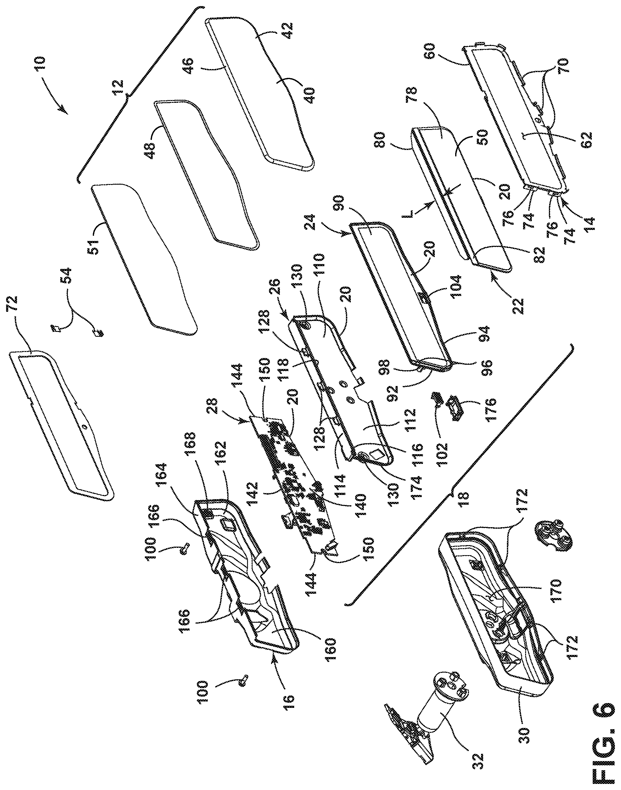
Referring now to FIGS. 1-3, reference numeral 10 generally designates a display mirror assembly for a vehicle. The display mirror assembly 10 includes a partially reflective, partially transmissive element 12 (also referred to as a "glass element" herein) and a display module 18 (FIG. 6) that is viewed through the partially reflective, partially transmissive element 12. As shown in FIG. 4, the display mirror assembly 10 further includes a front shield 14 and a rear shield 16 which shield and support the partially reflective, partially transmissive element 12 and the display module 18 (FIG. 6). As shown in FIGS. 5 and 6, the display module 18 generally includes several components 20, including a display 22, an optic block 24, a heat sink 26, and a primary printed circuit board (PCB) 28. A housing 30 at least partially receives the front shield 14, the display module 18, and the rear shield 16, and includes a mounting member 32 extending rearwardly therefrom. The mounting member 32 is adapted for mounting on a windshield of a vehicle. The housing may be configured to be part of the outer profile of the partially reflective, partially transmissive element.
Referring generally to FIGS. 1-5, the display mirror assembly 10 has a viewing area 40 disposed on a front surface of a front substrate 42 of the glass element 12. The viewing area 40 may be a rectangular shape, a trapezoidal shape, or any custom contoured shape desired for aesthetic reasons.
Referring to FIG. 4, the display mirror assembly 10 for a vehicle is shown, with the components partially exploded. The display mirror assembly 10 includes the glass element 12, the front shield 14 and the rear shield 16 encapsulating the display module 18, the rear housing 30, and the mounting member 32. As shown in FIGS. 4-6, the front shield 14, the rear shield 16, and components of the display module 18 include various retaining features to operably connect the several components of the display module 18 with the front shield 14, the rear shield 16 and each other, and to provide support to the display module 18. Specifically, the front shield 14 includes retaining features to operably connect the front shield 14 to the display module 18, and the rear shield 16 has retaining features to operably connect the rear shield 16 to the display module 18. The retaining features generally include snap fit connections, tab and slot connections, screw connections, and other known retaining features. Some or all of the retaining features may also be strengthened by the addition of adhesive compounds. Certain non-limiting illustrative examples of retaining features are described in detail herein.
The display mirror assembly 10 will hereafter be described in greater detail, beginning with the elements closest to the intended viewer, and extending rearwardly away from the viewer.
As shown in FIG. 4, the glass element 12 is generally planar, with an outer perimeter 46 and a border around the outer perimeter 46. The border may incorporate a peripheral concealing layer 48 or edge treatment, such as a chrome ring or other similar finish, to conceal a peripheral area of the front shield 14 and other elements located behind the glass element 12 in the display mirror assembly 10, including without limitation a seal on an electrochromic unit, an applique, foam adhesive, or pad printing. The border may extend from the outer perimeter 46 of the glass element 12 to an outer edge 50 of the display 22. Alternatively, the border may be narrower and not reach from the outer perimeter 46 to the outer edge 50 of the display 22 along at least some portions of the border. The outer perimeter 46 of the glass element 12 may also have a ground edge, a bezeled edge, or be frameless.
The glass element 12 may include an electro-optic element or include a prism-type construction. The prism-type construction generally includes one glass element 12 having a varying thickness from top to bottom. With an electro-optic element, the glass element 12 includes at least two glass substrates. For example, as illustrated in FIG. 6, the glass element 12 includes the front substrate 42 as well as a rear substrate 51. One non-limiting example of an electro-optic element is an electrochromic medium, which includes at least one solvent, at least one anodic material, and at least one cathodic material. Typically, both of the anodic and cathodic materials are electroactive and at least one of them is electrochromic. It will be understood that regardless of its ordinary meaning, the term "electroactive" will be defined herein as a material that undergoes a modification in its oxidation state upon exposure to a particular electrical potential difference. Additionally, it will be understood that the term "electrochromic" will be defined herein, regardless of its ordinary meaning, as a material that exhibits a change in its extinction coefficient at one or more wavelengths upon exposure to a particular electrical potential difference. Electrochromic components, as described herein, include materials whose color or opacity are affected by electric current, such that when an electrical current is applied to the material, the color or opacity change from a first phase to a second phase.
The electrochromic component as disclosed herein may be a single-layer, single-phase component, multi-layer component, or multi-phase component, as described in U.S. Pat. No. 5,928,572 entitled "Electrochromic Layer And Devices Comprising Same," U.S. Pat. No. 5,998,617 entitled "Electrochromic Compounds," U.S. Pat. No. 6,020,987 entitled "Electrochromic Medium Capable Of Producing A Pre-selected Color," U.S. Pat. No. 6,037,471 entitled "Electrochromic Compounds," U.S. Pat. No. 6,141,137 entitled "Electrochromic Media For Producing A Pre-selected Color," U.S. Pat. No. 6,241,916 entitled "Electrochromic System," U.S. Pat. No. 6,193,912 entitled "Near Infrared-Absorbing Electrochromic Compounds And Devices Comprising Same," U.S. Pat. No. 6,249,369 entitled "Coupled Electrochromic Compounds With Photostable Dication Oxidation States," and U.S. Pat. No. 6,137,620 entitled "Electrochromic Media With Concentration Enhanced Stability, Process For The Preparation Thereof and Use In Electrochromic Devices"; U.S. Patent Application Publication No. 2002/0015214 A1 entitled "Electrochromic Device," now U.S. Pat. No. 6,519,072; and International Patent Application Serial Nos. PCT/US98/05570 entitled "Electrochromic Polymeric Solid Films, Manufacturing Electrochromic Devices Using Such Solid Films, And Processes For Making Such Solid Films And Devices," PCT/EP98/03862 entitled "Electrochromic Polymer System," and PCT/US98/05570 entitled "Electrochromic Polymeric Solid Films, Manufacturing Electrochromic Devices Using Such Solid Films, And Processes For Making Such Solid Films And Devices," which are herein incorporated by reference in their entirety. The glass element 12 may also be any other element having partially reflective, partially transmissive properties. To provide electric current to the glass element 12, electrical elements 52 are provided on opposing sides of the element, to generate an electrical potential therebetween. A J-clip 54 is electrically engaged with each electrical element 52, and element wires extend from the J-clips 54 to the primary PCB 28.
Now referring to the embodiments illustrated in FIGS. 5 and 6, the front shield 14 and the rear shield 16 function to shield the display module 18 from radio frequency (RF) electromagnetic radiation and to provide support for the glass element 12 and the display module 18. The front shield 14 is formed from one or more materials which are suitable to block RF radiation, including without limitation steel. As a non-limiting example, the front shield 14 can be formed from a stamped steel material which is about 0.2 mm thick to 1.0 mm thick. In addition to preventing electromagnetic radiated emissions, the front shield 14 and the rear shield 16 also protect the circuitry of the device from electromagnetic susceptibility (conduction).
With reference again to FIGS. 5 and 6, the front shield 14 is generally shaped in the form of a ring 60 having an opening 62 therethrough. The front shield 14 has a front side 64, rear side 66, and an outer surface 68 which is generally coextensive with the outer perimeter 46 of the glass element 12. The front shield 14 includes retaining features 70 extending forwardly therefrom, to mechanically engage the glass element 12. An adhesive, such as a foam adhesive 72, may also be used to secure the glass element 12 to the front shield 14. The front shield 14 further includes rearwardly directed tabs 74 to operably engage the rear shield 16 (or a component of the display module 18). The rearwardly directed tabs 74 further include holes 76 therethrough, to operably engage at least one component of the display module 18, such as the optic block 24.
As clearly illustrated in FIG. 6, the display module 18 is disposed behind the front shield 14, with the display 22 viewable through the opening 62 in the front shield 14. The components of the display module 18 are ordered, from the front shield 14 toward the rear shield 16, in the following order: the display 22, the optic block 24, the heat sink 26, and the primary PCB 28.
The display 22 is generally planar, with the outer edge 50 defining a front surface 78. The front surface 78 of the display 22 can be shaped to correspond to and fit within the shape of the viewing area 40 of the display mirror assembly 10. Alternatively, the display 22 may have a front surface 78 which fits within, but is not complementary to the viewing area 40, for example, where the front surface 78 of the display 22 is generally rectangular and the front substrate 42 of the glass element 12 has a contoured outer perimeter 46. The distance between the outer edge 50 of the display 22 and the outer perimeter 46 of the glass element 12 is about 9 mm or less along at least a portion of the outer edge 50. In one embodiment, the display 22 has a viewable front surface 78 area which is about 56% to about 70% of the viewing area 40 of the glass element 12.
The display 22 may be a liquid crystal display (LCD), a light-emitting diode (LED), an organic light-emitting diode (OLED), plasma, digital light processing (DLP), or other display technology. The display 22 further includes a flexible electrical connector 80 which is operably mechanically and electrically connected with the primary PCB 28. The flexible electrical connector 80 has a length L that is sufficient to extend over and wrap around the display module components between the display 22 and the primary PCB 28, and has a width which extends substantially along a top edge 82 of the display 22. Ends of the flexible electrical connector 80 may be chamfered to ease manufacturing. The flexible electrical connector 80, when operably coupled to the primary PCB 28, aids in securing the components along a top edge of the display module 18.
As shown in FIGS. 5 and 6, the optic block 24 includes a front side 90 which is facing the display 22, a rear side 92 which is facing the heat sink 26, and an outer perimeter 94. The optic block 24 further includes tabs 96 extending generally outwardly therefrom around at least a portion of the outer perimeter 94. In the illustrated embodiment, the tabs 86 extend from sides of the optic block 24. However, it is contemplated that the tabs 96 could be located anywhere along the periphery of the optic block 24. The tabs 96 are received through the holes 76 in the rearwardly directed tabs 74 of the front shield 14, to operably couple the optic block 24 with the front shield 14. The optic block 24 further includes at least one receiving element 98 for receiving a mechanical fastener on the rear side 92 thereof. The receiving elements 98 are adapted to engage mechanical fasteners 100 threaded through the rear shield 16 and the display module 18 components between the optic block 24 and the rear shield 16. In alternate embodiments, the tabs 96 for engaging the front shield 14, the screw-receiving elements 98, or both, could be provided on different components of the display module 18.
As shown in FIGS. 4 and 6, a glare sensor optic 102 is provided on the front side 90 of the optic block 24, in a location which receives light through the glass element 12, and which is not behind the display 22. The glare sensor optic 102 is snap-fit into a receiving aperture 104 in the optic block 24. The glare sensor optic 102 receives light from headlamps of a trailing vehicle, and measures information regarding the likely glare visible on the glass element 12 and communicates this information to the display mirror assembly 10 so that the display mirror assembly 10 can be optimized to allow viewing of the display 22 through the glass element 12. The glare sensor optic's 102 optical vertical/horizontal pattern is symmetrical, so that orientation of the glare sensor optic 102 is not significant as shown in its circular geometry. The glare sensor optic 102 could also have an asymmetrical vertical/horizontal light gathering pattern, in which case a keyed feature would be put into the lens to verify correct orientation in the display mirror assembly 10. The glare sensor optic 102 could also be packaged at least partially within the housing 30 of the display mirror assembly 10 and have a light guide which is configured to propagate light to the glare sensor optic 102. The glare sensor optic 102 could also be an imager on a rear portion of the vehicle, wherein a signal representative of the received light is communicated from the glare sensor optic 102 to the display mirror assembly 10.
With reference again to FIGS. 5 and 6, the heat sink 26 is disposed rearwardly from the optic block 24, and dissipates heat generated by the primary PCB 28 and other components of the display module 18. The heat sink 26 has a generally planar body 110 with a front side 112 and a top edge 114. A channel 116 extends along the top edge 114 of the heat sink 26, and defines a forward-facing opening 118. An edge lit PCB 120 and a gap filler or thermal interface material 122 are disposed partially within the channel 116, with the edge lit PCB 120 extending generally perpendicularly from the heat sink 26 in a forward direction, and having an operable side which is facing downward, away from the top edge 114. The edge lit PCB 120 includes a wiring adapted for electrical connection with the primary PCB 28, to permit electrical power and signals to be supplied to the edge lit PCB 120. The gap filler 122 could be a gap filler pad, a thermally conductive epoxy, or other material used to increase the heat transfer from the edge lit PCB 120 to the heat sink 26. A plurality of tabs 128 extend upwardly from the top edge 114 of the heat sink 26, for mechanical engagement with the rear shield 16.
The heat sink 26 also includes at least one hole 130 therethrough to receive a mechanical fastener 100 threaded from the rear shield 16 to the optic block 24. The receiving element 98 of the optic block 24 is optionally raised, to extend through the at least one hole 130 in the heat sink 26 and receive the mechanical fastener 100. The receiving element 98 of the optic block 24 may also aid in alignment of the components of the display module 18 during manufacturing and will provide additional reinforcement to the display module 18 in the interaction between components if it is raised. Moreover, the receiving element 98 both secures the components of the display module 18 together and aids in maintaining proper spacing of the components.
The primary PCB 28 operates to provide electrical power and control for the components of the display module 18 and for the glass element 12. As shown in FIGS. 5 and 6, the primary PCB 28 is generally planar, with a front side 140, a rear side 142, and side edges 144. The front side 140 faces the heat sink 26 and the rear side 142 faces the rear shield 16. Electrical components are generally oriented on both sides of the primary PCB 28. The primary PCB 28 includes an electrical connector for operable electrical engagement with the electrical element wires of the glass element 12, an electrical connector for operable electrical engagement with the flexible electrical connector 80, and an electrical connector for operable electrical engagement with the wiring harness. Additional functional elements that may be provided on the display mirror assembly 10 may also be electrically connected to the primary PCB 28, such as the glare sensor optic 102 and any other functional buttons or features of the display mirror assembly 10. The primary PCB 28 further includes side cutouts 150 along the side edges 144, to permit passage of the mechanical fasteners 100 used to secure the rear shield 16 to the components of the display module 18.
With reference again to FIGS. 4 and 5, the rear shield 16 also serves to encapsulate the display module 18, and further interlock the components of the display mirror assembly 10. The rear shield 16 functions to shield the display module 18 from RF radiated and conducted emissions. The rear shield 16 is formed from a material which is suitable to block such radiation and provide the desired support for the display mirror assembly 10, such as steel. As a non-limiting example, the rear shield 16 can be formed from stamped steel with a thickness of about 0.2 to 1 mm. It is also contemplated that a welded or die-formed rear shield 16 could be provided.
As shown in FIG. 6, the rear shield 16 includes a rear wall 160 having an outer perimeter 162, and a peripheral wall 164 extending forward from the rear wall 160 about at least a portion of the outer perimeter 162. The peripheral wall 164 has slots 166 therein, which correspond to the upstanding tabs 128 along the top edge 114 of the heat sink 26 and are operably mechanically engageable therewith. The rear shield 16 further includes at least one hole 168 there through to accommodate the mechanical fastener 100, where the mechanical fastener 100 extends through the rear shield 16 and into the components of the display module 18 to secure the rear shield 16 to the display module 18. The mechanical fastener 100 extends through the rear wall 160 of the rear shield 16, through the side cutouts 150 of the primary PCB 28, through the heat sink 26, and is secured to the screw-receiving element 98 on the rear side 92 of the optic block 24.
As shown in FIG. 6, the rear housing 30 includes a forwardly directed cavity 170, into which all or a portion of the front shield 14, rear shield 16, and the display module 18 supported therebetween are inserted. The rear housing 30 includes mechanically engaging features 172 which snap fit with corresponding engagement features 174 located on the peripheral wall 164 of the rear housing 30 or on a display module 18 component such as the heat sink 26. The mounting member 32 is operably engaged with the rear housing 30 in any known manner.
With respect to the following description, the display mirror assembly 10 is considered "on axis" when a line perpendicular to the plane of the glass element 12 extends toward the eyes of a viewer. Due to the display 22 being viewed through the glass element 12, any glare on the glass element 12 may interfere with the visibility of the display 22. When the display mirror assembly 10 is on axis and is being used during night time driving conditions, headlights from a trailing vehicle (i.e., a vehicle driving behind the vehicle with the display mirror assembly 10) can cause a glare which is visible to the driver. According to one embodiment of the present disclosure, an actuator device 176, as shown in FIGS. 2 and 6, is operably coupled to the display mirror assembly 10. When actuated, the actuator device 176 moves at least the glass element 12 off axis (i.e., away from a direct line toward the driver's eyes). Typically, actuation of the actuator device 176 tilts the glass element 12 upwards, to move the mirror to an off-axis position. However, it should be appreciated that the actuator device 176 can be configured to move the mirror in any direction with respect to the axis. The actuator device 176 can also be configured to move the display 22 upon activation. The actuator device 176 can also be configured to turn the display 22 on or off. Thus, when the actuator device 176 is actuated to move the mirror off axis, the display 22 can be turned off. Typically, when the actuator device 176 is actuated, the display mirror assembly 10 rotates with the glass element 12 and the display 22, keeping a constant distance relationship to each other. When the actuator device 176 is activated, the mounting member 32 and flipper plate do not move with respect to the rest of the vehicle. In the illustrated embodiment, the glass element 12 and the display 22 are rigidly affixed to each other and do not move independently of one another. Alternatively, the glass element 12 could be configured to move independently of the display 22. Additionally, to provide information to the viewer of the display mirror assembly 10, the display mirror assembly 10 may include information regarding the field of view 178, such as a partially transmissive graphic overlay or an image on the display 22 visible on the viewing area 40 when the display mirror assembly 10 is in use.
In order to construct the display mirror assembly 10 described herein, the J-clips 54 are installed on the glass element 12, and then element wires are soldered to the top portion of the J-clips 54. The glass element 12 is then secured to the front side 64 of the front shield 14, using the foam adhesive 72 and the forward retaining features 70 of the front shield 14. The front shield 14 is then inverted, with the glass element 12 facing downwardly on a protective surface.
A first subassembly 180 (FIG. 5), including the display 22 and optic block 24, is assembled by snap-fitting the glare sensor optic 102 into the receiving aperture 104 in the optic block 24, and adhering the display 22 to the optic block 24. The adhesion of the display 22 and optic block 24 may include coating the front side 90 of the optic block 24 with an adhesive and applying a release liner over the adhesive, wherein the release liner is easily removable from the adhesive. When it is time to assemble the display 22 and optic block 24, the release liner is removed, and the display 22 is positioned on the front side 112 of the optic block 24. To position the display 22, one edge of the display 22 is aligned in the appropriate location on the optic block 24, and then the display 22 is rotated into contact with the front side 90 of the optic block 24. The first subassembly 180 is placed in position on the rear side 66 of the front shield 14. The tabs 96 extending outwardly from the optic block 24 are inserted through the holes 76 in the rearwardly directed tabs 74 of the front shield 14.
A second subassembly 182 (FIG. 5), including the heat sink 26 and edge lit PCB 120, is assembled. To assemble the second subassembly 182, the gap filler 122 is adhered to the edge lit PCB 120. The adhesion may include coating one side of the gap filler 122 with adhesive and then applying the gap filler 122 to the edge lit PCB 120 so that it does not interfere with the operable side of the edge lit PCB 120. The gap filler 122 and edge lit PCB 120 are then inserted into the opening in the channel 116 on the front side 112 of the heat sink 26. Locating features are optionally provided on the heat sink 26, the edge lit PCB 120 or both, to aid in inserting the side lit PCB and gap filler 122 into the channel 116. The second subassembly 182 is placed in position on the rear side 92 of the optic block 24. The screw-receiving elements 98 extending rearwardly from the optic block 24 extend through the holes 130 in the heat sink 26.
The primary PCB 28 is placed above the top edge of the second subassembly 182, with the front side 140 facing upwards. The flexible electrical connector 80 from the display 22 is mated with the electrical connector therefor. The primary PCB 28 is then rotated 180 degrees about the top edge of the second subassembly 182, so that the front side 140 is in contact with the heat sink 26. When rotating the primary PCB 28, the flexible electric connector is wrapped over the top edge of at least a portion of the display module 18. The element wires are electrically connected with the electrical connectors therefor, and the wiring harness for the edge lit PCB 120 is connected with the electrical connector therefor.
As shown in FIGS. 4 and 5, the rear shield 16 is placed over the primary PCB 28, and the tabs 128 extending upwardly from the heat sink 26 are engaged with the slots 166 on the peripheral wall 164 of the rear shield 16. At least one screw 100 is inserted through the screw holes 168 in the rear shield 16, through the side cutouts 150 in the PCB, through the heat sink 26, and into the screw-receiving elements 98 on the optic block 24. It is desirable that two to three screws 100 are affixed in this manner. Heat stakes or other mechanical fastening devices could be used to subassembly together.
The forwardly directed cavity 170 of the rear housing 30 is placed over the rear shield 16, and the mechanically engaging features 172 of the rear housing 30 are snap fit to engage with the corresponding engagement feature 174 of the heat sink 26. The mounting member 32 may be installed in the rear housing 30 prior to assembly.
The present disclosure may be used with a mounting system such as that described in U.S. Pat. Nos. 8,814,373; 8,201,800; and 8,210,695; U.S. Patent Application Publication Nos. 2014/0063630, now U.S. Pat. No. 9,174,577; 2013/0062497, now U.S. Pat. No. 9,019,197; and 2012/0327234, now U.S. Pat. No. 9,838,653; and U.S. Provisional Patent Application Nos. 61/709,716; 61/707,676; and 61/704,869, which are hereby incorporated herein by reference in their entirety. Further, the present disclosure may be used with a rearview packaging assembly such as that described in U.S. Pat. Nos. 8,814,373; 8,646,924; 8,643,931; and 8,264,761; U.S. Patent Application No. 2013/0194650, now U.S. Pat. No. 8,885,240; and U.S. Provisional Patent Application Nos. 61/707,625; and 61/590,259, which are hereby incorporated herein by reference in their entirety. Additionally, it is contemplated that the present disclosure can include a bezel such as that described in U.S. Pat. Nos. 8,827,517; 8,210,695; and 8,201,800, which are hereby incorporated herein by reference in their entirety.
The display mirror assembly according to the present disclosure has several advantages. The display module is supported by the front shield and rear shield, and does not require a separate support or carrier plate. Omission of a carrier plate, and inclusion of retaining features in the front shield and rear shield, permits the display mirror assembly to be lighter, involve less parts for manufacturing, and to have a display which is viewable over a larger percentage of the total viewing area of the display mirror assembly.
As shown in FIGS. 7A-7E, the display mirror assembly 10 can include one or more of the elements of FIGS. 1-6, and the housing 30 can be modified to be proud of the partially reflective, partially transmissive element 12. Additionally or alternatively, the display mirror assembly can include an external bi-modal switch 200 configured to at least one of activate and deactivate the display module 18 and alter a position of the partially reflective, partially transmissive element 12 to alternate between a first position and a second position.
As shown in FIGS. 7C and 7D, the bi-modal switch 200 can be located at the bottom of the housing 30. When the operator actuates the bi-modal switch 200, the display 22 is either activated or deactivated and/or the display mirror assembly 10 pivots between approximately 2 degrees and 7 degrees in the direction of the dotted lines, allowing for the display mirror assembly 10 to alternate between a first position and a second position. In one embodiment, it is contemplated that the operator could put the display mirror assembly 10 in the deactivated mode and adjust the position of the display mirror assembly 10 until the image in the partially reflective, partially transmissive element 12 is what could be expected to be seen when using a traditional mirror system. This will allow for the operator to immediately return to their desired reflective image when turning the display back to the off position. For purpose of explanation and not limitation, FIG. 7C generally illustrates a display mirror assembly 10 with the bi-modal switch 200 in the on position, which activates the display 22 and changes the angle of the partially reflective, partially transmissive element 12 with respect to an occupant. When the display 22 is on, the display mirror assembly 10 can be pivoted between approximately 2 degrees and 7 degrees an approximately vertical direction relative to the position the display mirror assembly 10 was in when off. FIG. 7D generally shows a display mirror assembly 10 with a bi-modal switch 200 in the off position, the partially reflective, partially transmissive element 12 is in the reflectance state so the user is viewing an image to the rear of the vehicle. Pivoting the display mirror assembly 10 when the display 22 is activated can reduce unwanted reflections that detract the displayed image. In both day and night time driving conditions, unwanted reflections can occur (e.g., backgrounds with high levels of ambient light, headlamps--the reflection may not line up with the headlamps shown in the display 22). Notably, if the display mirror assembly 10 was used without the bi-modal switch 200, the display mirror assembly 10 would likely be operated with the EC function as well. However, this causes color shift over the display 22 and causes other problems with trying to keep the display 22 intensity constant while the EC element is transitioning between dark and clear states.
Referring now to FIG. 7E, a cross-sectional view of a display mirror assembly includes a partially reflective, partially transmissive element 12, a display 22, an optic block 24, a heat sink 26, and a primary PCB 28. A housing 30 can at least partially receive the front shield 14, the display module 18, and the rear shield 16. An adhesive, such as but not limited to, a foam adhesive 72, may also be used to secure the glass element 12 to the front shield 14. The display module 18 and optic block 24 can be supported by a carrier or support plate 202 rather than only the front shield 14 and rear shield 16. The wall stock thickness of the carrier or support plate 202 can be approximately 1.5 mm, or alternatively, have a thickness anywhere from 1.0 mm to 2.0 mm, which can enhance the amount of viewable area of the display module 18 while maintaining adequate support for the display mirror assembly 10.
With reference to FIGS. 8A-9C, the bi-modal switch functionality consists of the interaction between the mounting member 32, a mounting member plate 34, a first pivot axis 300, a second pivot axis 302, a bi-modal switch spring 304, the bi-modal switch 200, the primary PCB 28, a display switch 306, the rear housing 30, the display 22, and the partially reflective, partially transmissive element 12, which are both rigidly attached to the rear housing 30. The first pivot axis 300 is defined by a cylindrical rotation member disposed between the rear housing 30 and the mounting member plate 34. The second pivot axis 302 is defined by a cylindrical rotation member disposed between the rear housing 30 and the bi-modal switch 200. The bi-modal switch 200 rotates about the second pivot axis 302 when the bi-modal switch 200 is moved from the on position to the off position. During the rotation of the bi-modal switch 200, the mounting member 32 and the mounting member plate 34 do not move relative to the observer of the display mirror assembly 10. However, the rear housing 30, the display 22, the primary PCB 28, and the partially reflective, partially transmissive element 12 rotate around the first pivot axis 300. The bi-modal switch 200 rotates approximately 75 to 105 degrees around the second pivot axis 302. The distance from the center of the second pivot axis 302 to a spring receiving area 308 of the bi-modal switch 200 and the bi-modal switch spring 304 is fairly small when compared to the distance between the first pivot axis 300 and the spring receiving area 308 between the bi-modal switch 200 and the bi-modal switch spring 304. The difference in distances between the first pivot axis 300 and the second pivot axis 302 causes a rotation of the rear housing 30 of approximately 2 to 7 degrees when the bi-modal switch 200 is rotated 75 to 110 degrees. The display switch 306 is rigidly mounted to the primary PCB 28 with a predetermined distance between the mounting member plate 34 and the display switch 306, such that when the bi-modal switch 200 is in the on position (FIGS. 7C and 8A-8C), the display switch 306 is not depressed, and when the bi-modal switch 200 is in the off position, the display switch 306 is depressed (FIGS. 7D and 9A-9C).
With reference again to FIGS. 8A-9C, the rotation of the bi-modal switch 200 generally performs two functions, the first of which is rotating the partially reflective, partially transmissive element 12 between 2 and 7 degrees, the second of which is to move the display switch 306 between depressed (activated) and not depressed (deactivated) positions, which switches the display 22 on and off, depending on the mode. Notably, the on/off depressed/not depressed state can be in either orientation and is not critical for the function of the display mirror assembly 10. Stated differently, the display switch 306 can be configured to activate the display 22 when depressed and deactivate the display 22 when not depressed. Alternatively, the display switch 306 can be configured to deactivate the display 22 when depressed and activate the display 22 when not depressed. In one embodiment, it is contemplated that when the display 22 is off and the mirror is rotated to optimize visibility of an image, the display switch 306 is in the off state and the display 22 is deactivated. When the bi-modal switch 200 is moved so that the reflected image is not optimized for visibility, the display switch 306 is in the on state and the display 22 is activated.
It will be appreciated that embodiments of the disclosure described herein may be comprised of one or more conventional processors and unique stored program instructions that control one or more processors to implement, in conjunction with certain non-processor circuits, some, most, or all of the functions of a display mirror assembly 10, as described herein. The non-processor circuits may include, but are not limited to signal drivers, clock circuits, power source circuits, and/or user input devices. As such, these functions may be interpreted as steps of a method used in using or constructing a classification system. Alternatively, some or all functions could be implemented by a state machine that has no stored program instructions, or in one or more application specific integrated circuits (ASICs), in which each function or some combinations of certain of the functions are implemented as custom logic. Of course, a combination of the two approaches could be used. Thus, the methods and means for these functions have been described herein. Further, it is expected that one of ordinary skill, notwithstanding possibly significant effort and many design choices motivated by, for example, available time, current technology, and economic considerations, when guided by the concepts and principles disclosed herein will be readily capable of generating such software instructions and programs and ICs with minimal experimentation.
It will be understood by one having ordinary skill in the art that construction of the described disclosure and other components is not limited to any specific material. Other exemplary embodiments of the disclosure disclosed herein may be formed from a wide variety of materials, unless described otherwise herein.
For purposes of this disclosure, the term "coupled" (in all of its forms, couple, coupling, coupled, etc.) generally means the joining of two components (electrical or mechanical) directly or indirectly to one another. Such joining may be stationary in nature or movable in nature. Such joining may be achieved with the two components (electrical or mechanical) and any additional intermediate members being integrally formed as a single unitary body with one another or with the two components. Such joining may be permanent in nature or may be removable or releasable in nature unless otherwise stated.
It is also important to note that the construction and arrangement of the elements of the disclosure as shown in the exemplary embodiments is illustrative only. Although only a few embodiments of the present innovations have been described in detail in this disclosure, those skilled in the art who review this disclosure will readily appreciate that many modifications are possible (e.g., variations in sizes, dimensions, structures, shapes and proportions of the various elements, values of parameters, mounting arrangements, use of materials, colors, orientations, etc.) without materially departing from the novel teachings and advantages of the subject matter recited. For example, elements shown as integrally formed may be constructed of multiple parts or elements shown as multiple parts may be integrally formed, the operation of the interfaces may be reversed or otherwise varied, the length or width of the structures and/or members or connector or other elements of the system may be varied, the nature or number of adjustment positions provided between the elements may be varied. It should be noted that the elements and/or assemblies of the system may be constructed from any of a wide variety of materials that provide sufficient strength or durability, in any of a wide variety of colors, textures, and combinations. Accordingly, all such modifications are intended to be included within the scope of the present innovations. Other substitutions, modifications, changes, and omissions may be made in the design, operating conditions, and arrangement of the desired and other exemplary embodiments without departing from the spirit of the present innovations.
It will be understood that any described processes or steps within described processes may be combined with other disclosed processes or steps to form structures within the scope of the present disclosure. The exemplary structures and processes disclosed herein are for illustrative purposes and are not to be construed as limiting.
It is also to be understood that variations and modifications can be made on the aforementioned structures and methods without departing from the concepts of the present disclosure, and further it is to be understood that such concepts are intended to be covered by the following claims unless these claims by their language expressly state otherwise.
* * * * *
D00000
D00001
D00002
D00003
D00004
D00005
D00006
D00007
D00008
D00009
D00010
D00011
D00012
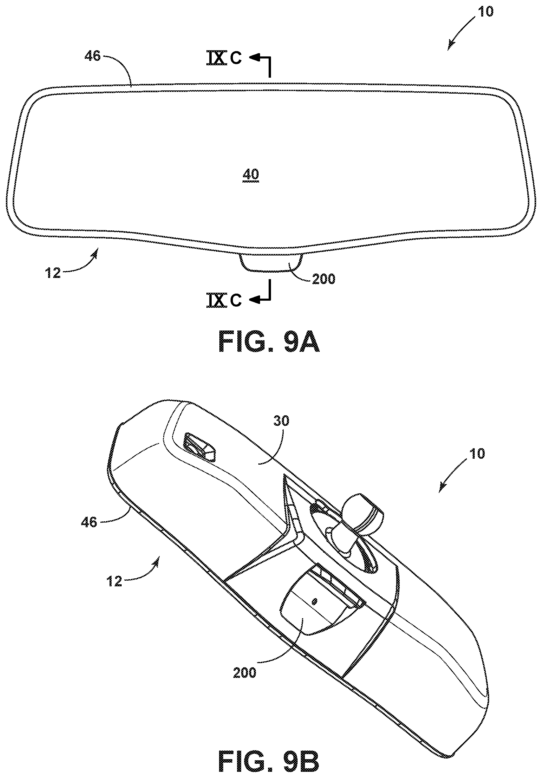
XML
uspto.report is an independent third-party trademark research tool that is not affiliated, endorsed, or sponsored by the United States Patent and Trademark Office (USPTO) or any other governmental organization. The information provided by uspto.report is based on publicly available data at the time of writing and is intended for informational purposes only.
While we strive to provide accurate and up-to-date information, we do not guarantee the accuracy, completeness, reliability, or suitability of the information displayed on this site. The use of this site is at your own risk. Any reliance you place on such information is therefore strictly at your own risk.
All official trademark data, including owner information, should be verified by visiting the official USPTO website at www.uspto.gov. This site is not intended to replace professional legal advice and should not be used as a substitute for consulting with a legal professional who is knowledgeable about trademark law.