X-ray phase contrast and dark-field information extraction with electric fringe scanning and/or active pixel processing
Wang , et al.
U.S. patent number 10,729,397 [Application Number 15/741,026] was granted by the patent office on 2020-08-04 for x-ray phase contrast and dark-field information extraction with electric fringe scanning and/or active pixel processing. This patent grant is currently assigned to Rensselaer Polutechnic Institute, University of Central Florida. The grantee listed for this patent is Rensselaer Polytechnic Institute, University of Central Florida. Invention is credited to Wenxiang Cong, Shuo Pang, Zaifeng Shi, Ge Wang.


| United States Patent | 10,729,397 |
| Wang , et al. | August 4, 2020 |
X-ray phase contrast and dark-field information extraction with electric fringe scanning and/or active pixel processing
Abstract
Novel and advantageous systems and methods for performing X-ray imaging by extracting X-ray phase-shift and/or dark-field information through a detector that has built-in G2 functionality are provided. Grating translation can be replaced by an electrical operation in the detection procedure, thereby eliminating the need for the analyzer grating and the typical mechanical stepping process.
| Inventors: | Wang; Ge (Loudonville, NY), Cong; Wenxiang (Albany, NY), Shi; Zaifeng (Tianjin, CN), Pang; Shuo (Oviedo, FL) | ||||||||||
|---|---|---|---|---|---|---|---|---|---|---|---|
| Applicant: |
|
||||||||||
| Assignee: | Rensselaer Polutechnic
Institute (Troy, NY) University of Central Florida (Orlando, FL) |
||||||||||
| Family ID: | 1000004961811 | ||||||||||
| Appl. No.: | 15/741,026 | ||||||||||
| Filed: | July 20, 2016 | ||||||||||
| PCT Filed: | July 20, 2016 | ||||||||||
| PCT No.: | PCT/US2016/043154 | ||||||||||
| 371(c)(1),(2),(4) Date: | December 29, 2017 | ||||||||||
| PCT Pub. No.: | WO2017/015381 | ||||||||||
| PCT Pub. Date: | January 26, 2017 |
Prior Publication Data
| Document Identifier | Publication Date | |
|---|---|---|
| US 20180192980 A1 | Jul 12, 2018 | |
Related U.S. Patent Documents
| Application Number | Filing Date | Patent Number | Issue Date | ||
|---|---|---|---|---|---|
| 62194452 | Jul 20, 2015 | ||||
| Current U.S. Class: | 1/1 |
| Current CPC Class: | A61B 6/4291 (20130101); A61B 6/4035 (20130101); A61B 6/484 (20130101); A61B 6/032 (20130101) |
| Current International Class: | A61B 6/00 (20060101); A61B 6/03 (20060101) |
References Cited [Referenced By]
U.S. Patent Documents
| 7453981 | November 2008 | Baumann et al. |
| 7492871 | February 2009 | Popescu et al. |
| 9066649 | June 2015 | Roessl et al. |
| 9600910 | March 2017 | Wang et al. |
| 9730657 | August 2017 | Wang et al. |
| 2015/0131783 | May 2015 | Sato |
| 2015/0157286 | June 2015 | Wang et al. |
| 2016/0041276 | February 2016 | Kawanabe |
| 2016/0113602 | April 2016 | Wang et al. |
| 2016/0135769 | May 2016 | Wang et al. |
| 2016/0166852 | June 2016 | Wang et al. |
| 2017/0043041 | February 2017 | Wang et al. |
| 2017/0360385 | December 2017 | Wang et al. |
| 2017/0362585 | December 2017 | Wang et al. |
| 0161324 | Nov 1985 | EP | |||
| 2014154188 | Oct 2014 | WO | |||
| 2015164405 | Oct 2015 | WO | |||
| 2016106348 | Jun 2016 | WO | |||
| 2016118960 | Jul 2016 | WO | |||
| 2016154136 | Sep 2016 | WO | |||
| 2016197127 | Dec 2016 | WO | |||
| 2017015381 | Jan 2017 | WO | |||
| 2017019782 | Feb 2017 | WO | |||
| 2017048856 | Mar 2017 | WO | |||
| 2017083849 | May 2017 | WO | |||
| 2017143247 | Aug 2017 | WO | |||
| 2017176976 | Oct 2017 | WO | |||
| 2017205379 | Nov 2017 | WO | |||
Other References
|
International Search Report/Written Opinion, PCT International Application No. PCT/US2016/043154, PCT/ISA/220, PCT/ISA/210, PCT/ISA/237, dated Nov. 1, 2016. cited by applicant. |
Primary Examiner: Kim; Christine S.
Attorney, Agent or Firm: Murtha Cullina LLP Gangemi; Anthony P.
Parent Case Text
CROSS-REFERENCE TO RELATED APPLICATIONS
This application is a national stage application of International Patent Application No. PCT/US2016/043154, filed Jul. 20, 2016 which claims the benefit of U.S. Provisional Application Ser. No. 62/194,452, filed Jul. 20, 2015, both of which are incorporated herein by reference in their entireties, including any figures, tables, and drawings.
Claims
What is claimed is:
1. An imaging system, comprising: an X-ray radiation source; and a detector for detecting X-ray radiation from the radiation source, wherein the detector comprises a semiconductor material and at least one electrode attached to the semiconductor material for providing an electric field; wherein the at least one electrode of the detector provides an electric field that steers electron-hole pairs horizontally in the semiconductor material of the detector.
2. The system according to claim 1, further comprising a phase grating positioned between the radiation source and the detector, and a source grating positioned between the radiation source and the phase grating, wherein the system is configured such that a subject to be imaged is positioned between the source grating and the phase grating.
3. The system according to claim 1, wherein the detector comprises a plurality of detector pixels, each comprising the semiconductor material of the detector, and wherein each pixel comprises at least one electrode attached to the semiconductor material.
4. The system according to claim 3, wherein each detector pixel further comprises an arithmetic unit connected to the at least one electrode, wherein each detector pixel further comprises an amplifier connected to the at least one electrode, and wherein each detector pixel further comprises an ADC connected to the at least one electrode.
5. The system according to claim 1, wherein the detector further comprises an arithmetic unit connected to the at least one electrode, wherein the detector further comprises an amplifier connected to the at least one electrode, and wherein the detector further comprises an analog-to-digital converter (ADC) connected to the at least one electrode.
6. The system according to claim 1, wherein the detector comprises a plurality of electrodes attached to the semiconductor material, and wherein the detector further comprises a plurality of amplifiers respectively connected to the plurality of electrodes.
7. The system according to claim 1, wherein the at least one electrode of the detector provides a homogenous electric field in the semiconductor material of the detector.
8. The system according to claim 1, wherein the detector comprises a plurality of electrodes, and wherein the electric field is added across 45% or less of the electrodes of the detector.
9. The system according to claim 1, wherein each electrode present is a micro-electrode, and wherein a length of each micro-electrode is half of a grating period of an analyzer grating whose functionality is incorporated into the detector.
10. The system according to claim 1, wherein the detector is a photon-counting detector, such that spectral information is included in data of the detector.
11. A method of imaging using the system according to claim 1, the method comprising: providing X-ray radiation to a sample to be imaged using the X-ray radiation source; collecting the X-ray radiation with the detector; and analyzing data from the detector to obtain an image.
12. The method according to claim 11, further comprising modulating the electric field provided by the at least one electrode attached to the semiconductor material of the detector, and wherein modulating the electric field comprises increasing or decreasing the voltage of the electric field from a zero voltage to a positive or negative voltage.
13. The method according to claim 12, further comprising detecting differently-shifted moire-fringe patterns at a plurality of time intervals while the electric field is modulated, thereby resulting in a recorded intensity measure as a function of voltage, and wherein the recorded intensity measure as a function of voltage is periodic with a period that is the same as a grating period of an analyzer grating whose functionality is incorporated into the detector.
14. The method according to claim 11, wherein analyzing data from the detector to obtain an image comprises extracting X-ray diffraction fringes, phase-shift information, and dark-field information from the data from the detector.
15. The method according to claim 11, wherein the detector comprises a plurality of detector pixels, and wherein analyzing data from the detector to obtain an image comprises using the recorded image intensity measure I(m,n,x.sub.v) at a given view angle to extract transmission, differential phase shift, and dark-field signals, respectively, where I(m,n,x.sub.v) is represented by the following Fourier series: I(m,n,x.sub.v).apprxeq.a.sub.0(m,n)+a.sub.1(m,n)cos(kx.sub.v+.phi.(m,n)), and wherein a phase angle .phi.(m,n) is directly related to a local gradient of a phase shift .differential..PHI..function..differential. ##EQU00003## where .PHI.(m,n) represents the phase shift of a wave front.
16. The method according to claim 11, wherein the detector is a photon-counting detector, such that spectral information is included in data of the detector.
17. An imaging system, comprising: an X-ray radiation source; and a detector for detecting X-ray radiation from the radiation source, wherein the detector comprises a semiconductor material and a plurality of electrodes attached to the semiconductor material for providing an electric field; wherein the electric field is added across 45% or less of the electrodes of the detector.
18. The system according to claim 17, wherein the detector further comprises an arithmetic unit connected to the at least one electrode, wherein the detector further comprises an amplifier connected to the at least one electrode, and wherein the detector further comprises an analog-to-digital converter (ADC) connected to the at least one electrode.
19. The system according to claim 17, wherein the detector comprises a plurality of detector pixels, each comprising the semiconductor material of the detector, and wherein each pixel comprises at least one electrode attached to the semiconductor material.
20. The system according to claim 19, wherein each detector pixel further comprises an arithmetic unit connected to the at least one electrode, wherein each detector pixel further comprises an amplifier connected to the at least one electrode, and wherein each detector pixel further comprises an ADC connected to the at least one electrode.
Description
BACKGROUND OF THE INVENTION
X-ray imaging is a powerful tool in many fundamental and practical applications. As a primary example, X-ray computed tomography (CT) is a cornerstone of modern hospitals and clinics. The dominating theory of X-ray imaging is generally based on the attenuation contrast mechanism.
X-ray gratings have been used for hybrid CT imaging in terms of attenuation, refraction, and small-angle scattering. This grating-based approach represents a paradigm shift in X-ray CT from gray-scale (attenuation) to true-color (attenuation, refraction, and small-angle scattering, which is also referred to as dark-field, and spectral) imaging.
In conventional X-ray imaging, the image contrast arises from varying linear attenuation coefficients. Attenuation-contrast-based imaging exhibits good performance only when strong attenuators are embedded in a weakly absorbing matrix, such as in the cases of bone-tissue and tissue-air interfaces. However, biological soft tissues include mainly light elements (e.g., hydrogen, carbon, nitrogen, and oxygen), and their compositions are quite homogeneous with little density variation. The attenuation-contrast between soft tissue features is often insufficient to reflect pathological changes.
In particular, many healthy tissues display similar characteristics in current X-ray images as those of diseased tissues, such as tumors. For example, fibro-glandular tissue can have a density of 1.035 cm.sup.-3 and an attenuation coefficient of 0.80 cm.sup.-1, and cancerous tissue can have a density of 1.045 cm.sup.-3 and an attenuation coefficient of 0.85 cm.sup.-1. Given inherent measurement noise, it is challenging to discern such cancerous tissue from the healthy tissue, as well as other soft tissue features such as those reflecting musculoskeletal healing. Therefore, attenuation-contrast-based imaging is unable to differentiate early-stage tumors and soft tissues.
X-ray small-angle scattering, or dark-field, imaging acquires photons slightly deflected from the primary beam through an object. Small-angle scattering signals reflect structural texture on length scales between 1 nanometer (nm) to several hundred nm. This imaging mode can reveal subtle texture of tissues. For example, the growth of tumors causes remarkable differences in small-angle scattering patterns from that of healthy tissues. It is clinically important that the structural variation in a tumor modifies the refractive index. The propagation of X-rays in a medium is characterized by the complex index of refraction. The cross section of an X-ray phase shift is one thousand times larger than that of the linear attenuation in the 20 keV-100 keV range. This implies that phase-contrast imaging has much higher sensitivity for light elements than does attenuation-contrast imaging.
The contrast-to-noise ratio of differential phase contrast CT images is superior to that of its attenuation-contrast CT counterpart. Therefore, phase-contrast imaging can observe unique critical structures of soft biological tissues. Moreover, the refractive index of tissues is inversely proportional to the square of the X-ray energy while the absorption coefficient decreases as the fourth power of the X-ray energy. Hence, X-ray phase-contrast imaging is suitable to operate at higher energies (e.g., >30 keV) for lower radiation dose than is attenuation imaging. Higher energy X-ray imaging can be useful for imaging and studies on large animals and/or human patients.
In X-ray grating-based imaging, X-ray phase-shift and dark-field information is currently extracted using the fringe scanning method through shifting of the analyzer grating. However, major challenges include the difficulty in making an analyzer grating (often known as G2), the requirement of a high-precision mechanical device, and the long data acquisition time due to the use of the phase stepping procedure.
BRIEF SUMMARY
Embodiments of the subject invention provide novel and advantageous systems and methods for performing X-ray imaging by extracting X-ray phase-shift and/or dark-field information through a detector that has built-in G2 functionality, as well as manipulation thereof. Grating translation can be replaced by an electrical operation in the detection procedure. That is, the typical mechanical stepping process can be omitted and replaced by an electrical steering process and/or mechanism, and the analyzer grating (G2) can be omitted by having its functionality combined with (or incorporated into) the detector itself. The systems and methods of embodiments of the subject invention present new opportunities in phase-contrast X-ray imaging (or X-ray grating-based imaging), shorten X-ray grating-based imaging time, increase dose utilization, and have many applications, including biomedical applications.
In an embodiment, an imaging system can comprise an X-ray radiation source and a detector for detecting X-ray radiation from the radiation source, wherein the detector comprises a semiconductor material and at least one electrode attached to the semiconductor material for providing an electric field. The system can further comprise a phase grating positioned between the radiation source and the detector, and a source grating positioned between the radiation source and the phase grating, and the system can specifically exclude an analyzer grating.
In another embodiment, a system as described herein can be used to perform a method of imaging, the method comprising: providing X-ray radiation to a sample to be imaged using the X-ray radiation source; collecting the X-ray radiation with the detector; and analyzing data from the detector to obtain an image. The electric field can be modulated by increasing or decreasing the voltage of the electric field from a zero voltage to a positive or negative voltage. Differently-shifted moire-fringe patterns can be detected at a plurality of time intervals while the electric field is modulated, thereby resulting in a recorded intensity measure as a function of voltage. X-ray diffraction fringes, phase-shift information, and dark-field information can be extracted from the data from the detector.
BRIEF DESCRIPTION OF THE DRAWINGS
FIG. 1 shows a grating-based X-ray interferometer that can be used in X-ray grating-based imaging.
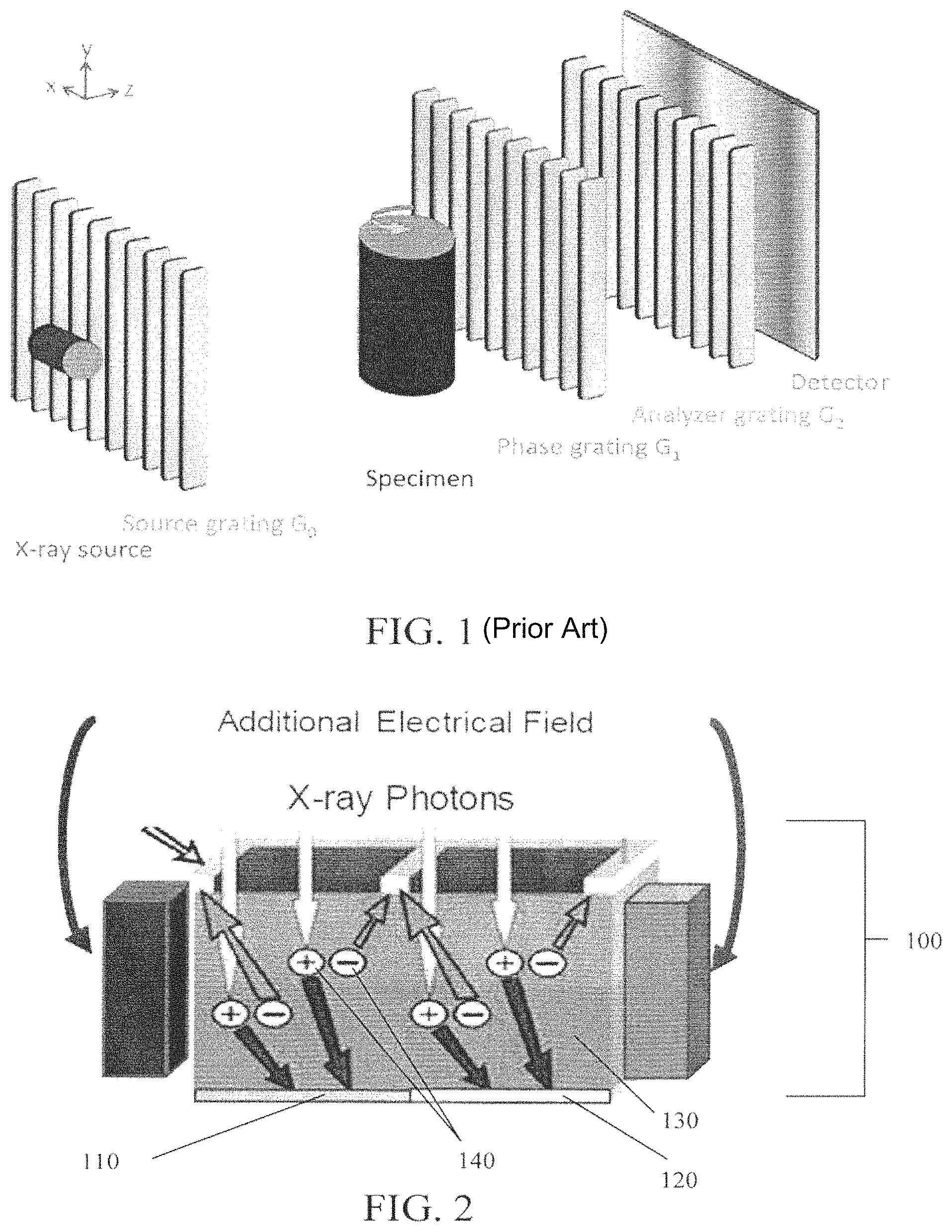
FIG. 2 shows a cross-sectional view of a detector according to an embodiment of the subject invention.
FIG. 3A shows an active pixel with according to embodiment of the subject invention.
FIG. 3B shows an active pixel with an identical electrode pattern to that of the active pixel in FIG. 3A.
FIG. 4 shows differential operation of a two-electrode readout pixel according to embodiment of the subject invention.
FIG. 5 shows a pixel having multiple electrodes according to an embodiment of the subject invention.
FIG. 6A shows configurations of a two-dimensional electrode array that can be implemented in a pixel of a detector according to an embodiment of the subject invention.
FIG. 6B shows configurations of a two-dimensional electrode array that can be implemented in a pixel of a detector according to an embodiment of the subject invention.
DETAILED DESCRIPTION
Embodiments of the subject invention provide novel and advantageous systems and methods for performing X-ray imaging by extracting X-ray phase-shift and/or dark-field information through a detector that has built-in G2 functionality, as well as manipulation thereof. Grating translation can be replaced by an electrical operation in the detection procedure. That is, the typical mechanical stepping process can be omitted and replaced by an electrical steering process and/or mechanism, and the analyzer grating (G2) can be omitted by having its functionality combined with (or incorporated into) the detector itself. The systems and methods of embodiments of the subject invention present new opportunities in phase-contrast X-ray imaging (or X-ray grating-based imaging), shorten X-ray grating-based imaging time, increase dose utilization, and have many applications, including biomedical applications. In some embodiments, the detector can be located at a Talbot distance, or fractional Talbot distance, from the phase grating, where the interference fringes are formed.
FIG. 1 shows a grating-based X-ray interferometer that can be used in X-ray grating-based imaging (phase-contrast X-ray imaging). FIG. 1 is from Burger et al. (Opt. Express 22, 32107-32118 2014; which is hereby incorporated herein by reference in its entirety). Referring to FIG. 1, the interferometer can include a phase grating G1 and an analyzer grating G2. The system can also include an X-ray source, a source grating G0, and a detector. The specimen being imaged can be placed between the source grating G0 and the phase grating G1. Phase-shift and dark-field information can be extracted using phase stepping, where the analyzer grating G2 or phase grating G1 is scanned over one G2 grating period.
According to embodiments of the subject invention, the analyzer grating G2 can be omitted by having its functionality combined with (or incorporated into) the detector itself. All the gratings can therefore be kept stationary, thereby decreasing scanning time and inhibiting the chances for mechanical error. The moire-fringe pattern can be shifted by varying an additional electric field across the detector (e.g., across a semiconductor material in a direct X-ray detector).
FIG. 2 shows a cross-sectional view of a detector according to an embodiment of the subject invention. Referring to FIG. 2, a detector pixel 100 of the detector 100 can have at least one electrode 110,120 connected to the bulk material 130 (e.g., semiconductor material) of the detector. When X-rays irradiate the semiconductor material 130 in the detector, photo-electrons are generated, producing electron-hole pairs 140 in the semiconductor material 130. The electrode(s) 110,120 connected to the semiconductor material 130 can acquire a current signal. Though FIG. 2 depicts two electrodes 110,120 connected to the bulk material 130 of the detector pixel 100, embodiments are not limited thereto. Each detector pixel can include a single electrode or a plurality of electrodes; such a plurality of electrodes can include two electrodes, three electrodes, four electrodes, or more. In a certain embodiment, the detector can have one electrode or the plurality of electrodes attached to the entire detector (instead of to each detector pixel).
In many embodiments, each electrode present in the detector can be a micro-electrode. The size of each micro-electrode can be, for example, half of the analyzer grating G2 period (i.e., the period of the analyzer grating G2 that would otherwise be present if its functionality was not combined with the detector).
The additional electric field can steer electron-hole pairs horizontally in the semiconductor material 130. Homogeneity of the electric field can be advantageous for the moire-fringe pattern to be shifted consistently; otherwise, further processing may be needed to extract required information. In an embodiment, to improve the homogeneity of the additional electric field, the electric field can be added across only a small number (e.g., 45% or less, 40% or less, 30% or less, 20% or less, 15% or less, 10% or less, or 5% or less) of electrodes attached to the semiconductor material 130 of the detector.
In the data acquisition process, the additional electric field can be modulated by increasing (or decreasing) the voltage of the electric field from a zero voltage to a positive or negative voltage so that differently-shifted moire-fringe patterns can be detected at various time intervals. The voltage setting can be optimized for a high signal-to-noise ratio. The recorded intensity measure as a function of voltage can be periodic with the same period of G2 (i.e., the period of the analyzer grating G2 that would otherwise be present if its functionality was not combined with the detector). From these data, the X-ray diffraction fringes, and the phase-shift and dark-field information, can be extracted in the same way as with the traditional stepping method.
Specifically, the intensity of the interference pattern in each detector pixel can be written as a Fourier series with negligible contributions of harmonics higher than the first order: I(m,n,x.sub.v).apprxeq.a.sub.0(m,n)+a.sub.1(m,n)cos(kx.sub.v+.phi.(m,n)). (1) Using Equation (1), the recorded image I(m, n, x.sub.v) at a given view angle can be used to extract transmission, differential phase shift, and dark-field signals, respectively. This can also be done using a photon-counting detector so that spectral information is included. The phase angle .phi.(m, n) is directly related to the local gradient of the phase shift
.differential..PHI..function..differential. ##EQU00001## where .PHI.(m, n) represents the phase shift of the wave front.
Though two electrodes are depicted in FIG. 2, single or multiple electrodes can be used, and their dimensions can be uniform or non-uniform (or some can be uniform while others are non-uniform). Also, in an embodiment, spacing between electrodes can be used, over which some electron-hole pairs may disappear at the cost of dose efficiency.
If electrodes are sufficiently small, no shifting will be needed, because the fringe pattern can be directly recorded. Such small electrodes and associated circuitry can be expensive in certain cases. In many embodiments of the subject invention, cost-effectiveness of the system or method can be optimized, which may not necessarily include using electrodes small enough such that no shifting is needed. Furthermore, the signals directly recorded by the electrodes can be processed for more information as described herein.
In some embodiments, the detector can include active pixel sensors. Active pixel sensors, in which each electrode has its own amplifier(s) and charge-to-voltage converter(s), are applicable in active X-ray phase-contrast imaging applications. Because the photo-electrons from each pixel can be extracted with multiple electrodes independently, the resulting signals can be processed to detect the sub-pixel shift of the X-ray fringes. Here, one pixel can be treated as the smallest unit of the sensor array, and the electrode patterns can be identical for each pixel as an example, though embodiments are not limited thereto (electrode patterns need not be identical for each pixel).
FIGS. 3A and 3B show two active pixels with identical electrode patterns. Referring to FIGS. 3A and 3B, each pixel includes two electrodes. Though an asymmetric configuration for the electrodes is depicted in FIGS. 3A and 3B, the electrodes can be symmetric or asymmetric to capture a sub-pixel intensity change. Each electrode can have its own amplifier and analog-to-digital converter (ADC). The signals from the electrodes after the analog-to-digital conversion can then be processed by an on-chip arithmetic unit to output a pixel value. The arithmetic unit can perform simple calculations, such as addition, subtraction, and multiplication, and it can also serve as a register, which performs a simple arithmetic operation on delayed input values. In various embodiments, each electrode can have its own arithmetic unit, each pixel can have a single arithmetic unit shared by all electrodes thereon, the chip can include a plurality of arithmetic units such that some pixels share the same arithmetic unit, or the chip can have a single arithmetic unit shared by all pixels and all electrodes.
FIG. 4 shows an example of a differential operation of a two-electrode 210,220 readout pixel, allowing detection of a sub-pixel phase-shift amplitude and direction. FIG. 4 demonstrates that both the sub-pixel phase stepping of the irradiance profile and the direction of the phase stepping (with an asymmetric electrode-pair) can be detected with a difference operation; i.e., the output signal is the difference between the signals from two electrodes 210,220, as shown in FIG. 4. Referring to FIG. 4 and assuming that there are two fringe periods on each pixel, the first electrode 210 has three quarters of the total pixel area while the second electrode 220 has one quarter of the pixel area. These proportions are for exemplary purposes only and should not be construed as limiting. At time t0, the applied voltage of the additional electric field V is less than 0, and the total signal in the area of the first electrode 210 is 1.5, while that of the second electrode 220 is 0.5. The intensity profile is shown on the left, above the electrodes 210,220. The readout signal after the arithmetic unit is 1. At time t1, the applied voltage is 0, and the readout signal is 0 as shown in the middle of the "difference signal" row of FIG. 4. At time t2, the applied voltage is greater than zero, and the charge at the second electrode 220 can only be partially converted to the readout, resulting in an asymmetric readout function, as shown in the plot at the bottom portion of FIG. 4. During the data acquisition process, the shift voltage can drive a scan over one period of the X-ray diffraction fringe, and the phase contrast information can be easily computed.
FIG. 5 shows a pixel having multiple electrodes (m electrodes, where m is an integer) according to an embodiment of the subject invention. Though FIG. 5 depicts the electrodes having uniform area, embodiments are not limited thereto. Finer sub-pixel shift can be detected by using multiple electrodes, as in FIG. 5. If the periodicity of the X-ray fringes and the pixel electrodes matches, a simple difference between signals from two adjacent electrodes can be used to calculate both differential phase-shift and dark-field information.
FIGS. 6A and 6B show configurations of two-dimensional electrode arrays that can be implemented in pixels of a detector according to embodiments of the subject invention. Referring to FIG. 6A, the electrodes of the array can have different areas as depicted, though embodiments are not limited thereto. Also, though FIG. 6A depicts four electrodes in the array, this is for exemplary purposes only. Referring to FIG. 6B, the areas of the electrodes can be uniform. Also, any reasonable number of electrodes can be present in the array. These two-dimensional configurations can be implemented to measure diffraction fringes on a plane.
According to embodiments of the subject invention, X-ray phase-shift and dark-field information can be extracted through a specially-designed detector that has built-in analyzer grating G2 functionality and manipulation. Grating translation can be replaced by an electrical operation in the detection procedure. The mechanical stepping process of the conventional art can be replaced by the electric steering mechanism, and the actual analyzer grating G2 can be omitted by having its functionality incorporated into the detector of the imaging system. The detector can be located at a Talbot distance, or a fractional Talbot distance, from the phase grating, where the interference fringes are formed, though embodiments are not limited thereto.
The methods and processes described herein can be embodied as code and/or data. The software code and data described herein can be stored on one or more computer-readable media, which may include any device or medium that can store code and/or data for use by a computer system. When a computer system reads and executes the code and/or data stored on a computer-readable medium, the computer system performs the methods and processes embodied as data structures and code stored within the computer-readable storage medium.
It should be appreciated by those skilled in the art that computer-readable media include removable and non-removable structures/devices that can be used for storage of information, such as computer-readable instructions, data structures, program modules, and other data used by a computing system/environment. A computer-readable medium includes, but is not limited to, volatile memory such as random access memories (RAM, DRAM, SRAM); and non-volatile memory such as flash memory, various read-only-memories (ROM, PROM, EPROM, EEPROM), magnetic and ferromagnetic/ferroelectric memories (MRAM, FeRAM), and magnetic and optical storage devices (hard drives, magnetic tape, CDs, DVDs); network devices; or other media now known or later developed that is capable of storing computer-readable information/data. Computer-readable media should not be construed or interpreted to include any propagating signals. A computer-readable medium of the subject invention can be, for example, a compact disc (CD), digital video disc (DVD), flash memory device, volatile memory, or a hard disk drive (HDD), such as an external HDD or the HDD of a computing device, though embodiments are not limited thereto. A computing device can be, for example, a laptop computer, desktop computer, server, cell phone, or tablet, though embodiments are not limited thereto.
The subject invention includes, but is not limited to, the following exemplified embodiments.
Embodiment 1
An imaging system, comprising:
a radiation source (e.g., an X-ray source); and
a detector for detecting radiation (e.g., X-rays) from the radiation source, wherein the detector comprises a semiconductor material and at least one electrode attached to the semiconductor material for providing an electric field.
Embodiment 2
The system according to embodiment 1, further comprising a phase grating positioned between the radiation source and the detector.
Embodiment 3
The system according to embodiment 2, further comprising a source grating positioned between the radiation source and the phase grating.
Embodiment 4
The system according to embodiment 3, configured such that the subject to be imaged is positioned between the source grating and the phase grating.
Embodiment 5
The system according to embodiment 1, further comprising a source grating positioned between the radiation source and the detector.
Embodiment 6
The system according to any of embodiments 1-5, wherein the system excludes an analyzer grating.
Embodiment 7
The system according to any of embodiments 1-6, wherein the detector comprises a plurality of detector pixels, each comprising the semiconductor material of the detector, and wherein each detector pixel comprises at least one electrode attached to the semiconductor material.
Embodiment 8
The system according to embodiment 7, wherein each detector pixel comprises a plurality of electrodes attached to the semiconductor material.
Embodiment 9
The system according to embodiment 7, wherein each detector pixel comprises exactly two electrodes attached to the semiconductor material.
Embodiment 10
The system according to any of embodiments 1-9, wherein the detector further comprises an arithmetic unit connected to the at least one electrode.
Embodiment 11
The system according to any of embodiments 1-10, wherein the detector further comprises an amplifier connected to the at least one electrode.
Embodiment 12
The system according to any of embodiments 1-11, wherein the detector further comprises an analog-to-digital convertor (ADC) connected to the at least one electrode.
Embodiment 13
The system according to embodiment 9, wherein the detector further comprises an amplifier connected to the at least one electrode between the arithmetic unit and the at least one electrode.
Embodiment 14
The system according to any of embodiments 9 and 13, wherein the detector further comprises an ADC connected to the at least one electrode between the arithmetic unit and the at least one electrode.
Embodiment 15
The system according to any of embodiments 1-10, wherein the detector comprises a plurality of electrodes attached to the semiconductor material, and wherein the detector further comprises a plurality of amplifiers respectively connected to the plurality of electrodes.
Embodiment 16
The system according to any of embodiments 1-10 and 15, wherein the detector comprises a plurality of electrodes attached to the semiconductor material, and wherein the detector further comprises a plurality of ADCs respectively connected to the plurality of electrodes.
Embodiment 17
The system according to embodiment 9, wherein the detector comprises a plurality of electrodes attached to the semiconductor material, and wherein the detector further comprises a plurality of amplifiers respectively connected to the plurality of electrodes between the arithmetic unit and the respective electrode.
Embodiment 18
The system according to any of embodiments 9, wherein the detector comprises a plurality of electrodes attached to the semiconductor material, and wherein the detector further comprises a plurality of ADCs respectively connected to the plurality of electrodes between the arithmetic unit and the respective electrode.
Embodiment 19
The system according to any of embodiments 7-9, wherein each detector pixel further comprises an arithmetic unit connected to the at least one electrode.
Embodiment 20
The system according to any of embodiments 7-9 and 19, wherein each detector pixel further comprises an amplifier connected to the at least one electrode.
Embodiment 21
The system according to any of embodiments 7-9, 19, and 20, wherein each detector pixel further comprises an ADC connected to the at least one electrode.
Embodiment 22
The system according to embodiment 19, wherein each detector pixel further comprises an amplifier connected to the at least one electrode between the arithmetic unit and the at least one electrode.
Embodiment 23
The system according to any of embodiments 19 and 22, wherein each detector pixel further comprises an ADC connected to the at least one electrode between the arithmetic unit and the at least one electrode.
Embodiment 24
The system according to any of embodiments 7-9 and 19, wherein each detector pixel comprises a plurality of electrodes attached to the semiconductor material, and wherein each detector pixel further comprises a plurality of amplifiers respectively connected to the plurality of electrodes.
Embodiment 25
The system according to any of embodiments 7-9, 19, and 24, wherein each detector pixel comprises a plurality of electrodes attached to the semiconductor material, and wherein each detector pixel further comprises a plurality of ADCs respectively connected to the plurality of electrodes.
Embodiment 26
The system according to embodiment 19, wherein each detector pixel comprises a plurality of electrodes attached to the semiconductor material, and wherein each detector pixel further comprises a plurality of amplifiers respectively connected to the plurality of electrodes between the arithmetic unit and the respective electrode.
Embodiment 27
The system according to embodiment 19, wherein each detector pixel comprises a plurality of electrodes attached to the semiconductor material, and wherein each detector pixel further comprises a plurality of ADCs respectively connected to the plurality of electrodes between the arithmetic unit and the respective electrode.
Embodiment 28
The system according to any of embodiments 7-9, wherein each detector pixel comprises a plurality of electrodes attached to the semiconductor material, and wherein each detector pixel further comprises a plurality of arithmetic units respectively connected to the plurality of electrodes.
Embodiment 29
The system according to embodiment 28, wherein each detector pixel further comprises a plurality of amplifiers respectively connected to the plurality of electrodes between the respective arithmetic unit and the respective electrode.
Embodiment 30
The system according to any of embodiments 28-29, wherein each detector pixel further comprises a plurality of ADCs respectively connected to the plurality of electrodes between the respective arithmetic unit and the respective electrode.
Embodiment 31
The system according to any of embodiments 7-30, wherein each detector pixel comprises a plurality of electrodes attached to the semiconductor material and arranged in an array within said detector pixel.
Embodiment 32
The system according to any of embodiments 7-31, wherein each detector pixel comprises a plurality of electrodes attached to the semiconductor material, and wherein an area of each electrode within a given detector pixel is the same as that of all other electrodes within said detector pixel.
Embodiment 33
The system according to any of embodiments 1-32, wherein the detector comprises a plurality of electrodes attached to the semiconductor material, and wherein an area of each electrode is the same as that of all other electrodes.
Embodiment 34
The system according to any of embodiments 7-31, wherein each detector pixel comprises a plurality of electrodes attached to the semiconductor material, and wherein an area of each electrode within a given detector pixel is different from that of at least one other electrode within said detector pixel.
Embodiment 35
The system according to any of embodiments 7-31 and 34, wherein each detector pixel comprises a plurality of electrodes attached to the semiconductor material, and wherein an area of each electrode within a given detector pixel is different from that of all other electrodes within said detector pixel.
Embodiment 36
The system according to any of embodiments 1-31, 34, and 35, wherein the detector comprises a plurality of electrodes attached to the semiconductor material, and wherein an area of each electrode is the different from that of at least one other electrode.
Embodiment 37
The system according to any of embodiments 1-31 and 34-36, wherein the detector comprises a plurality of electrodes attached to the semiconductor material, and wherein an area of each electrode is the different from that of all other electrodes.
Embodiment 38
The system according to any of embodiments 1-37, wherein the electrode(s) present in the detector provide an electric field that steers electron-hole pairs horizontally (parallel to a detection surface of the detector that faces the radiation source) in the semiconductor material of the detector.
Embodiment 39
The system according to any of embodiments 1-38, wherein the electrode(s) present in the detector provide a homogenous electric field in the semiconductor material of the detector.
Embodiment 40
The system according to any of embodiments 1-39, wherein the detector comprises a plurality of electrodes, and wherein the electric field is added across 45% or less of the electrodes of the detector.
Embodiment 41
The system according to any of embodiments 1-39, wherein the detector comprises a plurality of electrodes, and wherein the electric field is added across 40% or less of the electrodes of the detector.
Embodiment 42
The system according to any of embodiments 1-39, wherein the detector comprises a plurality of electrodes, and wherein the electric field is added across 30% or less of the electrodes of the detector.
Embodiment 43
The system according to any of embodiments 1-39, wherein the detector comprises a plurality of electrodes, and wherein the electric field is added across 20% or less of the electrodes of the detector.
Embodiment 44
The system according to any of embodiments 1-39, wherein the detector comprises a plurality of electrodes, and wherein the electric field is added across 15% or less of the electrodes of the detector.
Embodiment 45
The system according to any of embodiments 1-39, wherein the detector comprises a plurality of electrodes, and wherein the electric field is added across 10% or less of the electrodes of the detector.
Embodiment 46
The system according to any of embodiments 1-39, wherein the detector comprises a plurality of electrodes, and wherein the electric field is added across 5% or less of the electrodes of the detector.
Embodiment 47
The system according to any of embodiments 1-46, wherein each electrode present is a micro-electrode.
Embodiment 48
The system according to embodiment 47, wherein the size (e.g., length, width, or longest dimension in any direction) of each micro-electrode is half of the grating period of the (omitted) analyzer grating whose functionality is incorporated into the detector.
Embodiment 49
The system according to any of embodiments 1-48, wherein the system further comprises a phase grating positioned between the X-ray source and the detector, and wherein the detector is positioned a Talbot distance, or fractional Talbot distance, from the phase grating, where the interference fringes are formed.
Embodiment 50
A method of imaging using the system according to any of embodiments 1-49, the method comprising:
providing radiation (e.g., X-ray radiation) to a sample to be imaged using the radiation source;
collecting the radiation (e.g., X-ray radiation) with the detector; and analyzing data from the detector to obtain an image.
Embodiment 51
The method according to embodiment 52, further comprising modulating the electric field provided by the at least one electrode attached to the semiconductor material of the detector.
Embodiment 52
The method according to embodiment 51, wherein modulating the electric field comprises increasing (or decreasing) the voltage of the electric field from a zero voltage to a positive (or negative) voltage.
Embodiment 53
The method according to embodiment 52, further comprising detecting differently-shifted moire-fringe patterns at a plurality of time intervals while the electric field is modulated, thereby resulting in a recorded intensity measure as a function of voltage.
Embodiment 54
The method according to embodiment 53, wherein the recorded intensity measure as a function of voltage is periodic with a period that is the same as the grating period of the (omitted) analyzer grating whose functionality is incorporated into the detector.
Embodiment 55
The method according to any of embodiments 50-54, wherein analyzing data from the detector to obtain an image comprises extracting diffraction fringes (e.g., X-ray diffraction fringes), phase-shift information, and dark-field information from the data from the detector.
Embodiment 56
The method according to any of embodiments 50-55, wherein the detector comprises a plurality of detector pixels, and wherein analyzing data from the detector to obtain an image comprises using the recorded image intensity measure I(m, n, x.sub.v) at a given view angle to extract transmission, differential phase shift, and dark-field signals, respectively, where I(m, n, x.sub.v) is represented by the following Fourier series: I(m,n,x.sub.v).apprxeq.a.sub.0(m,n)+a.sub.1(m,n)cos(kx.sub.v+.phi.(m,n)).
Embodiment 57
The method according to embodiment 56, wherein the phase angle .phi.(m, n) is directly related to the local gradient of the phase shift
.differential..PHI..function..differential. ##EQU00002## where .PHI.(m, n) represents the phase shift of the wave front.
Embodiment 58
The system according to any of embodiments 1-49, further comprising a (non-transitory) machine readable medium (e.g., computer readable medium) having machine-executable (e.g., computer executable) instructions (stored thereon) for performing the step of analyzing data from the detector according to the method of any of embodiments 50-57, wherein the machine readable medium is in operable communication with the detector.
Embodiment 59
The system according to any of embodiments 1-49 and 58, or the method according to any of embodiments 50-57, wherein the detector is a photon-counting detector, such that spectral information is included in data of the detector.
It should be understood that the examples and embodiments described herein are for illustrative purposes only and that various modifications or changes in light thereof will be suggested to persons skilled in the art and are to be included within the spirit and purview of this application.
All patents, patent applications, provisional applications, and publications referred to or cited herein (including those in the "References" section) are incorporated by reference in their entirety, including all figures and tables, to the extent they are not inconsistent with the explicit teachings of this specification.
REFERENCES
Shi et al., An edge-on charge-transfer design for energy-resolved x-ray detection, Physics in Medicine and Biology, Volume 61, Number 11, 2016 Wang et al., International Patent Application Publication No. WO2016/106348 Wang et al., U.S. Patent Application Publication No. 2015/0157286 Wang et al., U.S. Patent Application Publication No. 2015/0170361 Wang et al., U.S. Patent Application Publication No. 2015/0193927 Wang et al., International Patent Application Publication No. WO2015/164405 Wang et al., U.S. Patent Application Publication No. 2016/0113602 Wang et al., U.S. Patent Application Publication No. 2016/0135769 Wang et al., U.S. Patent Application Publication No. 2016/0166852 Wang et al., International Patent Application Publication No. WO2016/106348 Wang et al., International Patent Application No. PCT/US2016/014769 Wang et al., International Patent Application No. PCT/US2016/023460 Wang et al., International Patent Application No. PCT/US2016/036057 Burger et al., "Regularized iterative integration combined with non-linear diffusion filtering for phase-contrast x-ray computed tomography," Opt. Express 22, 32107-32118 (2014); http://www.opticsinfobase.org/oe/abstract.cfm?uri=oe-22-26-32107 U.S. Provisional Application Ser. No. 62/197,301
* * * * *
References
D00000
D00001
D00002
D00003
M00001
M00002
M00003
XML
uspto.report is an independent third-party trademark research tool that is not affiliated, endorsed, or sponsored by the United States Patent and Trademark Office (USPTO) or any other governmental organization. The information provided by uspto.report is based on publicly available data at the time of writing and is intended for informational purposes only.
While we strive to provide accurate and up-to-date information, we do not guarantee the accuracy, completeness, reliability, or suitability of the information displayed on this site. The use of this site is at your own risk. Any reliance you place on such information is therefore strictly at your own risk.
All official trademark data, including owner information, should be verified by visiting the official USPTO website at www.uspto.gov. This site is not intended to replace professional legal advice and should not be used as a substitute for consulting with a legal professional who is knowledgeable about trademark law.