Differential sensing in an active stylus
Sundara-Rajan , et al.
U.S. patent number 10,725,564 [Application Number 13/434,596] was granted by the patent office on 2020-07-28 for differential sensing in an active stylus. This patent grant is currently assigned to Wacom Co., Ltd.. The grantee listed for this patent is Yassar Ali, James D. Lyle, Igor Polishchuk, Kishore Sundara-Rajan. Invention is credited to Yassar Ali, James D. Lyle, Igor Polishchuk, Kishore Sundara-Rajan.

| United States Patent | 10,725,564 |
| Sundara-Rajan , et al. | July 28, 2020 |
Differential sensing in an active stylus
Abstract
In one embodiment, a stylus receives a first signal from a first electrode of the stylus, the stylus being operable to communicate wirelessly with a device through a touch sensor of the device; receives a second signal from a second electrode of the stylus, the second signal being a reference signal and the second electrode being a reference electrode; and compares the first signal with the second signal.
| Inventors: | Sundara-Rajan; Kishore (San Jose, CA), Ali; Yassar (Sunnyvale, CA), Polishchuk; Igor (Fremont, CA), Lyle; James D. (Santa Clara, CA) | ||||||||||
|---|---|---|---|---|---|---|---|---|---|---|---|
| Applicant: |
|
||||||||||
| Assignee: | Wacom Co., Ltd. (Saitama,
JP) |
||||||||||
| Family ID: | 47070902 | ||||||||||
| Appl. No.: | 13/434,596 | ||||||||||
| Filed: | March 29, 2012 |
Prior Publication Data
| Document Identifier | Publication Date | |
|---|---|---|
| US 20130106798 A1 | May 2, 2013 | |
Related U.S. Patent Documents
| Application Number | Filing Date | Patent Number | Issue Date | ||
|---|---|---|---|---|---|
| 61553114 | Oct 28, 2011 | ||||
| Current U.S. Class: | 1/1 |
| Current CPC Class: | G06F 3/0383 (20130101); G06F 3/03545 (20130101) |
| Current International Class: | G06F 3/0354 (20130101); G06F 3/038 (20130101) |
| Field of Search: | ;345/179 ;327/365,517 ;726/16 ;401/29,32,99,179,195 ;178/19.01 |
References Cited [Referenced By]
U.S. Patent Documents
| 3958234 | May 1976 | Hoo |
| 4695680 | September 1987 | Kable |
| 5973677 | October 1999 | Gibbons |
| 7612767 | November 2009 | Griffin |
| 7663607 | February 2010 | Hotelling |
| 7785027 | August 2010 | McKinley et al. |
| 7864503 | January 2011 | Chang |
| 7875814 | January 2011 | Chen |
| 7920129 | April 2011 | Hotelling |
| 8031094 | October 2011 | Hotelling |
| 8031174 | October 2011 | Hamblin |
| 8040326 | October 2011 | Hotelling |
| 8049732 | November 2011 | Hotelling |
| 8179381 | May 2012 | Frey |
| 8217902 | July 2012 | Chang et al. |
| 8723824 | May 2014 | Myers et al. |
| 2008/0055279 | March 2008 | Osada et al. |
| 2008/0238885 | October 2008 | Zachut |
| 2008/0309635 | December 2008 | Matsuo |
| 2009/0065268 | March 2009 | Katsurahira |
| 2009/0095540 | April 2009 | Zachut |
| 2009/0115725 | May 2009 | Shemesh |
| 2009/0127005 | May 2009 | Zachut |
| 2009/0153152 | June 2009 | Maharyta |
| 2009/0184939 | July 2009 | Wohlstadter |
| 2009/0251434 | October 2009 | Rimon |
| 2009/0315854 | December 2009 | Matsuo |
| 2010/0006350 | January 2010 | Elias |
| 2010/0155153 | June 2010 | Zachut |
| 2010/0292945 | November 2010 | Reynolds |
| 2010/0315384 | December 2010 | Hargreaves et al. |
| 2011/0007029 | January 2011 | Ben-David |
| 2011/0043281 | February 2011 | Golden |
| 2012/0062521 | March 2012 | Ahn |
| 2012/0105362 | May 2012 | Kremin |
| 2012/0146958 | June 2012 | Oda |
| 2012/0154340 | June 2012 | Vuppu |
| 2012/0161846 | June 2012 | Ningrat |
| 2012/0242588 | September 2012 | Myers |
| 2012/0242592 | September 2012 | Rothkopf |
| 2012/0243151 | September 2012 | Lynch |
| 2012/0243719 | September 2012 | Franklin |
| 2012/0327041 | December 2012 | Harley |
| 2012/0327042 | December 2012 | Harley et al. |
| 2012/0331546 | December 2012 | Falkenburg et al. |
| 2013/0076612 | March 2013 | Myers |
| 2018/0173331 | June 2018 | Kremin |
| WO 2012/129247 | Sep 2012 | WO | |||
Other References
|
Kyung, Ki-Uk et al., "wUbi-Pen : Windows Graphical User Interface Interacting with Haptic Feedback Stylus," SIGGRAPH,, Los Angeles, California, Aug. 2008. cited by applicant . Lee, Johnny C. et al., "Haptic Pen: A Tactile Feedback Stylus for Touch Screens," UIST '04, vol. 6, Issue 2, Santa Fe, New Mexico, Oct. 2004. cited by applicant . Song, Hyunyoung et al., "Grips and Gestures on a Multi-Touch Pen," CHI 2011, Session: Flexible Grips & Gestures, Vancouver, BC, Canada, May 2011. cited by applicant . Tan, Eng Chong et al., "Application of Capacitive Coupling to the Design of an Absolute-Coordinate Pointing Device," IEEE Transactions on Instrumentation and Measurement, vol. 54, No. 5, Oct. 2005. cited by applicant . U.S. Appl. No. 61/454,936, filed Mar. 21, 2011, Myers. cited by applicant . U.S. Appl. No. 61/454,950, filed Mar. 21, 2011, Lynch. cited by applicant . U.S. Appl. No. 61/454,894, filed Mar. 21, 2011, Rothkopf. cited by applicant. |
Primary Examiner: Shah; Priyank J
Attorney, Agent or Firm: Seed IP Law Group LLP
Parent Case Text
RELATED APPLICATION
This application claims the benefit, under 35 U.S.C. .sctn. 119(e), of U.S. Provisional Patent Application No. 61/553,114, filed 28 Oct. 2011, which is incorporated herein by reference.
Claims
What is claimed is:
1. A method comprising: receiving, wirelessly with a first electrode of a stylus, a first signal comprising a signal component, the stylus being operable to communicate wirelessly with a device via the first electrode and through a touch sensor of the device; receiving a second signal from a second electrode of the stylus, the second signal comprising a signal component, the first signal and second signal each containing noise having similar characteristics, wherein the first electrode spans between a first distal end and a first proximal end along a longitudinal axis of the stylus, the second electrode spans between a second distal end and a second proximal end along the longitudinal axis of the stylus, and the first proximal end of the first electrode is located distal to the second distal end of the second electrode along the longitudinal axis of the stylus, wherein the first electrode and the second electrode are concentrically arranged about the longitudinal axis of the stylus, and wherein the signal component of the first signal is a first version of a device signal (S) and the signal component of the second signal is a second version of the device signal S; removing noise from the first signal by subtracting the second signal from the first signal, including generating an output that is the difference between the first signal and the second signal; determining the signal component of the first signal based on the output and the signal component of the second signal; and synchronizing the stylus with the device using a bit sequence extracted from the determined signal component of the first signal.
2. The method of claim 1, wherein comparing the first signal with the second signal comprises comparing the first signal with the second signal using an operational amplifier of the stylus.
3. The method of claim 1, wherein comparing the first signal with the second signal comprises comparing the first signal with the second signal using a digital comparator of the stylus.
4. The method of claim 1, wherein the first electrode and the second electrode interpose a third electrode in-between along the longitudinal axis of the stylus.
5. The method of claim 1, comprising: transmitting, wirelessly with at least one of the first electrode and the second electrode of the stylus, a third signal to the device, in response to the bit sequence transmitted by the device as a synchronization signal.
6. A non-transitory computer-readable medium comprising logic, the logic configured to, when executed by one or more processors, cause the one or more processors to perform operations comprising: receiving, wirelessly with a first electrode of a stylus, a first signal comprising a signal component, the stylus being operable to communicate wirelessly with a device via the first electrode and through a touch sensor of the device; receiving a second signal from a second electrode of the stylus, the second signal comprising a signal component, the first signal and second signal each containing noise having similar characteristics, wherein the first electrode spans between a first distal end and a first proximal end along a longitudinal axis of the stylus, the second electrode spans between a second distal end and a second proximal end along the longitudinal axis of the stylus, and the first proximal end of the first electrode is located distal to the second distal end of the second electrode along the longitudinal axis of the stylus wherein the first electrode and the second electrode are concentrically arranged about the longitudinal axis of the stylus, and wherein the signal component of the first signal is a first version of a device signal (S) and the signal component of the second signal is a second version of the device signal S; removing noise from the first signal by subtracting the second signal from the first signal, including generating an output that is the difference between the first signal and the second signal; determining the signal component of the first signal based on the output and the signal component of the second signal; and synchronizing the stylus with the device using a bit sequence extracted from the determined signal component of the first signal.
7. The non-transitory computer-readable medium of claim 6, wherein the first electrode is located in a tip region of the stylus.
8. The non-transitory computer-readable medium of claim 6, wherein comparing the first signal with the second signal comprises comparing the first signal with the second signal using an operational amplifier.
9. The non-transitory computer-readable medium of claim 6, wherein comparing the first signal with the second signal comprises comparing the first signal with the second signal using a digital comparator.
10. The non-transitory computer-readable medium of claim 6, wherein the stylus is further operable to multiply by a gain factor the output of the comparison of the first signal with the second signal.
11. The non-transitory computer-readable medium of claim 6, wherein the first electrode and the second electrode interpose a third electrode in-between along the longitudinal axis of the stylus.
12. The non-transitory computer-readable medium of claim 6, wherein the operations comprise: transmitting, wirelessly with at least one of the first electrode and the second electrode of the stylus, a third signal to the device, in response to the bit sequence transmitted by the device as a synchronization signal.
13. A stylus comprising: a plurality of electrodes; a non-transitory computer-readable medium comprising logic, the logic configured to, when executed by one or more processors, cause the one or more processors to perform operations comprising: receiving, wirelessly with a first electrode of the plurality of electrodes, a first signal comprising a signal component, the signal component of the first signal having an unknown quantity, the stylus being operable to communicate wirelessly with a device via the first electrode and through a touch sensor of the device; receiving a second signal from a second electrode of the stylus, the second signal comprising a signal component, the first signal and second signal each containing noise having similar characteristics, the signal component of the second signal associated with a known quantity, wherein the first electrode spans between a first distal end and a first proximal end along a longitudinal axis of the stylus, the second electrode spans between a second distal end and a second proximal end along the longitudinal axis of the stylus, and the first proximal end of the first electrode is located distal to the second distal end of the second electrode along the longitudinal axis of the stylus, wherein the first electrode and the second electrode are concentrically arranged about the longitudinal axis of the stylus, and wherein the signal component of the first signal is a first version of a device signal (S) and the signal component of the second signal is a second version of the device signal S; removing noise from the first signal by subtracting the second signal from the first signal, including generating an output that is the difference between the first signal and the second signal; determining the unknown quantity of the signal component of the first signal based on the output and the known quantity associated with the signal component of the second signal; and synchronizing the stylus with the device using a bit sequence extracted from the determined signal component of the first signal.
14. The stylus of claim 13, wherein the first electrode is located in the tip of the stylus.
15. The stylus of claim 13, wherein comparing the first signal with the second signal comprises comparing the first signal with the second signal using an operational amplifier.
16. The stylus of claim 13, wherein comparing the first signal with the second signal comprises comparing the first signal with the second signal using a digital comparator.
17. The stylus of claim 13, wherein the stylus is further operable to multiply by a gain factor the output of the comparison of the first signal with the second signal.
18. The stylus of claim 13, wherein determining the unknown quantity of the signal component of the first signal based on the output and the known quantity associated with the signal component of the second signal comprises summing the output and the known quantity associated with the signal component of the second signal.
19. The stylus of claim 13, wherein the first electrode and the second electrode interpose a third electrode in-between along the longitudinal axis of the stylus.
20. The stylus of claim 13, wherein the operations comprise: transmitting, wirelessly with at least one of the first electrode and the second electrode of the stylus, a third signal to the device, in response to the bit sequence transmitted by the device as a synchronization signal.
Description
TECHNICAL FIELD
This disclosure generally relates to touch sensors.
BACKGROUND
A touch sensor may detect the presence and location of a touch or the proximity of an object (such as a user's finger or a stylus) within a touch-sensitive area of the touch sensor overlaid on a display screen, for example. In a touch sensitive display application, the touch sensor may enable a user to interact directly with what is displayed on the screen, rather than indirectly with a mouse or touch pad. A touch sensor may be attached to or provided as part of a desktop computer, laptop computer, tablet computer, personal digital assistant (PDA), smartphone, satellite navigation device, portable media player, portable game console, kiosk computer, point-of-sale device, or other suitable device. A control panel on a household or other appliance may include a touch sensor.
There are a number of different types of touch sensors, such as, for example, resistive touch screens, surface acoustic wave touch screens, and capacitive touch screens. Herein, reference to a touch sensor may encompass a touch screen, and vice versa, where appropriate. When an object touches or comes within proximity of the surface of the capacitive touch screen, a change in capacitance may occur within the touch screen at the location of the touch or proximity. A touch-sensor controller may process the change in capacitance to determine its position on the touch screen.
BRIEF DESCRIPTION OF THE DRAWINGS
FIG. 1 illustrates an example touch sensor with an example touch-sensor controller.
FIG. 2 illustrates an example active stylus exterior.
FIG. 3 illustrates an example active stylus interior.
FIG. 4 illustrates an example active stylus with touch sensor device.
FIG. 5 illustrates an example active stylus tip.
FIG. 6 illustrates an example method for differential sensing in an active stylus.
DESCRIPTION OF EXAMPLE EMBODIMENTS
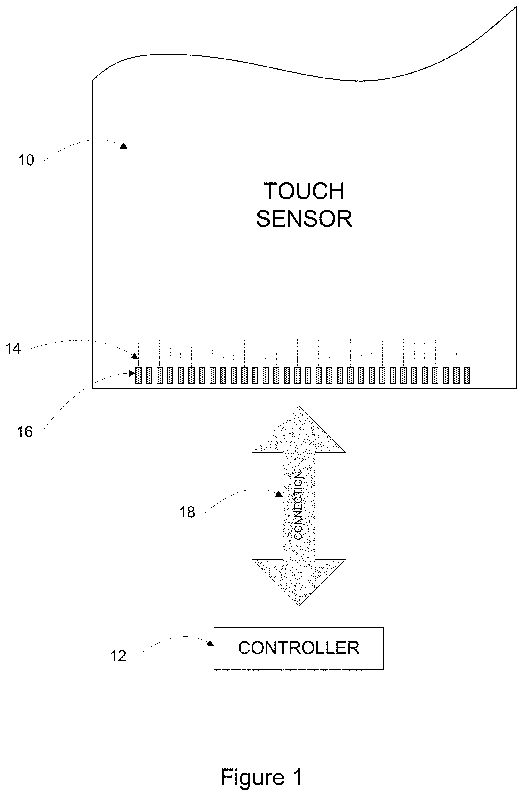
FIG. 1 illustrates an example touch sensor 10 with an example touch-sensor controller 12. Touch sensor 10 and touch-sensor controller 12 may detect the presence and location of a touch or the proximity of an object within a touch-sensitive area of touch sensor 10. Herein, reference to a touch sensor may encompass both the touch sensor and its touch-sensor controller, where appropriate. Similarly, reference to a touch-sensor controller may encompass both the touch-sensor controller and its touch sensor, where appropriate. Touch sensor 10 may include one or more touch-sensitive areas, where appropriate. Touch sensor 10 may include an array of drive and sense electrodes (or an array of electrodes of a single type) disposed on one or more substrates, which may be made of a dielectric material. Herein, reference to a touch sensor may encompass both the electrodes of the touch sensor and the substrate(s) that they are disposed on, where appropriate. Alternatively, where appropriate, reference to a touch sensor may encompass the electrodes of the touch sensor, but not the substrate(s) that they are disposed on.
An electrode (whether a ground electrode, a guard electrode, a drive electrode, or a sense electrode) may be an area of conductive material forming a shape, such as for example a disc, square, rectangle, thin line, other suitable shape, or suitable combination of these. One or more cuts in one or more layers of conductive material may (at least in part) create the shape of an electrode, and the area of the shape may (at least in part) be bounded by those cuts. In particular embodiments, the conductive material of an electrode may occupy approximately 100% of the area of its shape. As an example and not by way of limitation, an electrode may be made of indium tin oxide (ITO) and the ITO of the electrode may occupy approximately 100% of the area of its shape (sometimes referred to as 100% fill), where appropriate. In particular embodiments, the conductive material of an electrode may occupy substantially less than 100% of the area of its shape. As an example and not by way of limitation, an electrode may be made of fine lines of metal or other conductive material (FLM), such as for example copper, silver, or a copper- or silver-based material, and the fine lines of conductive material may occupy approximately 5% of the area of its shape in a hatched, mesh, or other suitable pattern. Herein, reference to FLM encompasses such material, where appropriate. Although this disclosure describes or illustrates particular electrodes made of particular conductive material forming particular shapes with particular fill percentages having particular patterns, this disclosure contemplates any suitable electrodes made of any suitable conductive material forming any suitable shapes with any suitable fill percentages having any suitable patterns. Where appropriate, the shapes of the electrodes (or other elements) of a touch sensor may constitute in whole or in part one or more macro-features of the touch sensor. One or more characteristics of the implementation of those shapes (such as, for example, the conductive materials, fills, or patterns within the shapes) may constitute in whole or in part one or more micro-features of the touch sensor. One or more macro-features of a touch sensor may determine one or more characteristics of its functionality, and one or more micro-features of the touch sensor may determine one or more optical features of the touch sensor, such as transmittance, refraction, or reflection.
A mechanical stack may contain the substrate (or multiple substrates) and the conductive material forming the drive or sense electrodes of touch sensor 10. As an example and not by way of limitation, the mechanical stack may include a first layer of optically clear adhesive (OCA) beneath a cover panel. The cover panel may be clear and made of a resilient material suitable for repeated touching, such as for example glass, polycarbonate, or poly(methyl methacrylate) (PMMA). This disclosure contemplates any suitable cover panel made of any suitable material. The first layer of OCA may be disposed between the cover panel and the substrate with the conductive material forming the drive or sense electrodes. The mechanical stack may also include a second layer of OCA and a dielectric layer (which may be made of PET or another suitable material, similar to the substrate with the conductive material forming the drive or sense electrodes). As an alternative, where appropriate, a thin coating of a dielectric material may be applied instead of the second layer of OCA and the dielectric layer. The second layer of OCA may be disposed between the substrate with the conductive material making up the drive or sense electrodes and the dielectric layer, and the dielectric layer may be disposed between the second layer of OCA and an air gap to a display of a device including touch sensor 10 and touch-sensor controller 12. As an example only and not by way of limitation, the cover panel may have a thickness of approximately 1 millimeter (mm); the first layer of OCA may have a thickness of approximately 0.05 mm; the substrate with the conductive material forming the drive or sense electrodes may have a thickness of approximately 0.05 mm; the second layer of OCA may have a thickness of approximately 0.05 mm; and the dielectric layer may have a thickness of approximately 0.05 mm. Although this disclosure describes a particular mechanical stack with a particular number of particular layers made of particular materials and having particular thicknesses, this disclosure contemplates any suitable mechanical stack with any suitable number of any suitable layers made of any suitable materials and having any suitable thicknesses. As an example and not by way of limitation, in particular embodiments, a layer of adhesive or dielectric may replace the dielectric layer, second layer of OCA, and air gap described above, with there being no air gap to the display.
One or more portions of the substrate of touch sensor 10 may be made of polyethylene terephthalate (PET) or another suitable material. This disclosure contemplates any suitable substrate with any suitable portions made of any suitable material. In particular embodiments, the drive or sense electrodes in touch sensor 10 may be made of ITO in whole or in part. In particular embodiments, the drive or sense electrodes in touch sensor 10 may be made of fine lines of metal or other conductive material. As an example and not by way of limitation, one or more portions of the conductive material may be copper or copper-based and have a thickness of approximately 5 microns (.mu.m) or less and a width of approximately 10 .mu.m or less. As another example, one or more portions of the conductive material may be silver or silver-based and similarly have a thickness of approximately 5 .mu.m or less and a width of approximately 10 .mu.m or less. This disclosure contemplates any suitable electrodes made of any suitable material.
Touch sensor 10 may implement a capacitive form of touch sensing. In a mutual-capacitance implementation, touch sensor 10 may include an array of drive and sense electrodes forming an array of capacitive nodes. A drive electrode and a sense electrode may form a capacitive node. The drive and sense electrodes forming the capacitive node may come near each other, but not make electrical contact with each other. Instead, the drive and sense electrodes may be capacitively coupled to each other across a space between them. A pulsed or alternating voltage applied to the drive electrode (by touch-sensor controller 12) may induce a charge on the sense electrode, and the amount of charge induced may be susceptible to external influence (such as a touch or the proximity of an object). When an object touches or comes within proximity of the capacitive node, a change in capacitance may occur at the capacitive node and touch-sensor controller 12 may measure the change in capacitance. By measuring changes in capacitance throughout the array, touch-sensor controller 12 may determine the position of the touch or proximity within the touch-sensitive area(s) of touch sensor 10.
In a self-capacitance implementation, touch sensor 10 may include an array of electrodes of a single type that may each form a capacitive node. When an object touches or comes within proximity of the capacitive node, a change in self-capacitance may occur at the capacitive node and touch-sensor controller 12 may measure the change in capacitance, for example, as a change in the amount of charge needed to raise the voltage at the capacitive node by a pre-determined amount. As with a mutual-capacitance implementation, by measuring changes in capacitance throughout the array, touch-sensor controller 12 may determine the position of the touch or proximity within the touch-sensitive area(s) of touch sensor 10. This disclosure contemplates any suitable form of capacitive touch sensing, where appropriate.
In particular embodiments, one or more drive electrodes may together form a drive line running horizontally or vertically or in any suitable orientation. Similarly, one or more sense electrodes may together form a sense line running horizontally or vertically or in any suitable orientation. In particular embodiments, drive lines may run substantially perpendicular to sense lines. Herein, reference to a drive line may encompass one or more drive electrodes making up the drive line, and vice versa, where appropriate. Similarly, reference to a sense line may encompass one or more sense electrodes making up the sense line, and vice versa, where appropriate.
Touch sensor 10 may have drive and sense electrodes disposed in a pattern on one side of a single substrate. In such a configuration, a pair of drive and sense electrodes capacitively coupled to each other across a space between them may form a capacitive node. For a self-capacitance implementation, electrodes of only a single type may be disposed in a pattern on a single substrate. In addition or as an alternative to having drive and sense electrodes disposed in a pattern on one side of a single substrate, touch sensor 10 may have drive electrodes disposed in a pattern on one side of a substrate and sense electrodes disposed in a pattern on another side of the substrate. Moreover, touch sensor 10 may have drive electrodes disposed in a pattern on one side of one substrate and sense electrodes disposed in a pattern on one side of another substrate. In such configurations, an intersection of a drive electrode and a sense electrode may form a capacitive node. Such an intersection may be a location where the drive electrode and the sense electrode "cross" or come nearest each other in their respective planes. The drive and sense electrodes do not make electrical contact with each other--instead they are capacitively coupled to each other across a dielectric at the intersection. Although this disclosure describes particular configurations of particular electrodes forming particular nodes, this disclosure contemplates any suitable configuration of any suitable electrodes forming any suitable nodes. Moreover, this disclosure contemplates any suitable electrodes disposed on any suitable number of any suitable substrates in any suitable patterns.
As described above, a change in capacitance at a capacitive node of touch sensor 10 may indicate a touch or proximity input at the position of the capacitive node. Touch-sensor controller 12 may detect and process the change in capacitance to determine the presence and location of the touch or proximity input. Touch-sensor controller 12 may then communicate information about the touch or proximity input to one or more other components (such one or more central processing units (CPUs)) of a device that includes touch sensor 10 and touch-sensor controller 12, which may respond to the touch or proximity input by initiating a function of the device (or an application running on the device). Although this disclosure describes a particular touch-sensor controller having particular functionality with respect to a particular device and a particular touch sensor, this disclosure contemplates any suitable touch-sensor controller having any suitable functionality with respect to any suitable device and any suitable touch sensor.
Touch-sensor controller 12 may be one or more integrated circuits (ICs), such as for example general-purpose microprocessors, microcontrollers, programmable logic devices or arrays, application-specific ICs (ASICs). In particular embodiments, touch-sensor controller 12 comprises analog circuitry, digital logic, and digital non-volatile memory. In particular embodiments, touch-sensor controller 12 is disposed on a flexible printed circuit (FPC) bonded to the substrate of touch sensor 10, as described below. The FPC may be active or passive, where appropriate. In particular embodiments, multiple touch-sensor controllers 12 are disposed on the FPC. Touch-sensor controller 12 may include a processor unit, a drive unit, a sense unit, and a storage unit. The drive unit may supply drive signals to the drive electrodes of touch sensor 10. The sense unit may sense charge at the capacitive nodes of touch sensor 10 and provide measurement signals to the processor unit representing capacitances at the capacitive nodes. The processor unit may control the supply of drive signals to the drive electrodes by the drive unit and process measurement signals from the sense unit to detect and process the presence and location of a touch or proximity input within the touch-sensitive area(s) of touch sensor 10. The processor unit may also track changes in the position of a touch or proximity input within the touch-sensitive area(s) of touch sensor 10. The storage unit may store programming for execution by the processor unit, including programming for controlling the drive unit to supply drive signals to the drive electrodes, programming for processing measurement signals from the sense unit, and other suitable programming, where appropriate. Although this disclosure describes a particular touch-sensor controller having a particular implementation with particular components, this disclosure contemplates any suitable touch-sensor controller having any suitable implementation with any suitable components.
Tracks 14 of conductive material disposed on the substrate of touch sensor 10 may couple the drive or sense electrodes of touch sensor 10 to connection pads 16, also disposed on the substrate of touch sensor 10. As described below, connection pads 16 facilitate coupling of tracks 14 to touch-sensor controller 12. Tracks 14 may extend into or around (e.g. at the edges of) the touch-sensitive area(s) of touch sensor 10. Particular tracks 14 may provide drive connections for coupling touch-sensor controller 12 to drive electrodes of touch sensor 10, through which the drive unit of touch-sensor controller 12 may supply drive signals to the drive electrodes. Other tracks 14 may provide sense connections for coupling touch-sensor controller 12 to sense electrodes of touch sensor 10, through which the sense unit of touch-sensor controller 12 may sense charge at the capacitive nodes of touch sensor 10. Tracks 14 may be made of fine lines of metal or other conductive material. As an example and not by way of limitation, the conductive material of tracks 14 may be copper or copper-based and have a width of approximately 100 .mu.m or less. As another example, the conductive material of tracks 14 may be silver or silver-based and have a width of approximately 100 .mu.m or less. In particular embodiments, tracks 14 may be made of ITO in whole or in part in addition or as an alternative to fine lines of metal or other conductive material. Although this disclosure describes particular tracks made of particular materials with particular widths, this disclosure contemplates any suitable tracks made of any suitable materials with any suitable widths. In addition to tracks 14, touch sensor 10 may include one or more ground lines terminating at a ground connector (which may be a connection pad 16) at an edge of the substrate of touch sensor 10 (similar to tracks 14).
Connection pads 16 may be located along one or more edges of the substrate, outside the touch-sensitive area(s) of touch sensor 10. As described above, touch-sensor controller 12 may be on an FPC. Connection pads 16 may be made of the same material as tracks 14 and may be bonded to the FPC using an anisotropic conductive film (ACF). Connection 18 may include conductive lines on the FPC coupling touch-sensor controller 12 to connection pads 16, in turn coupling touch-sensor controller 12 to tracks 14 and to the drive or sense electrodes of touch sensor 10. In other embodiments, connection pads 16 may be connected to an electro-mechanical connector (such as a zero insertion force wire-to-board connector). In these embodiments, connection 18 may not need to include an FPC. This disclosure contemplates any suitable connection 18 between touch-sensor controller 12 and touch sensor 10.
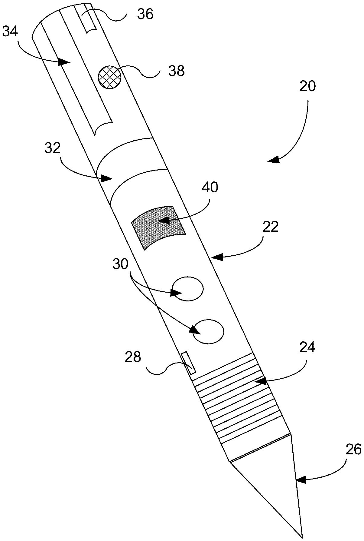
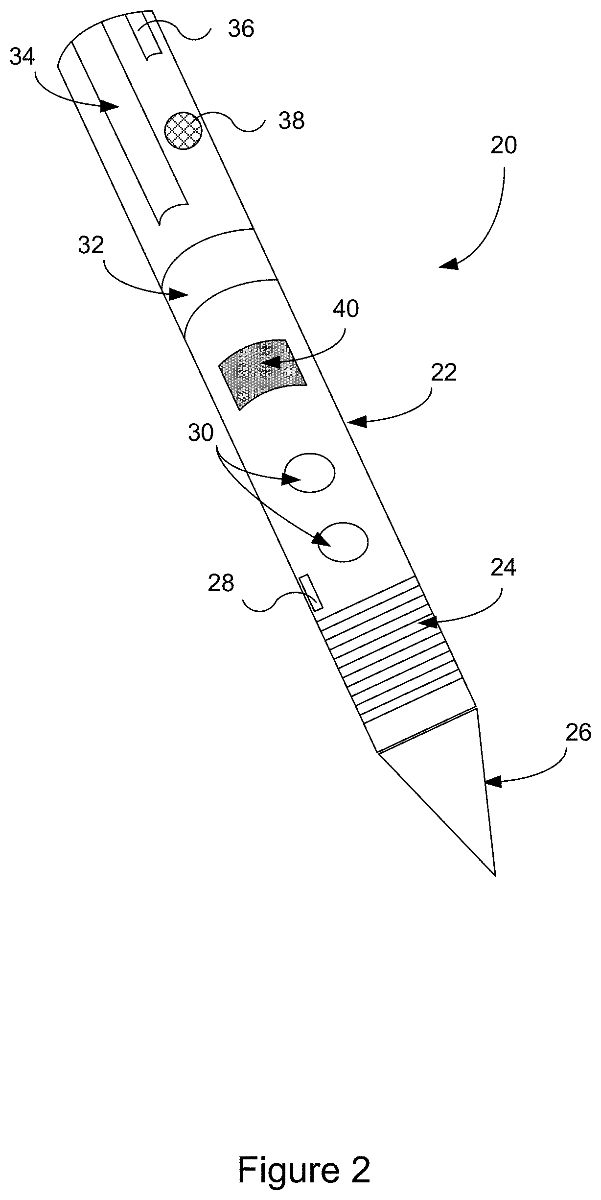
FIG. 2 illustrates an example exterior of an example active stylus 20. In particular embodiments, active stylus 20 is powered (e.g., by an internal or external power source) and is capable of providing touch or proximity inputs to a touch sensor (e.g., touch sensor 10 illustrated in FIG. 1). Active stylus 20 may include one or more components, such as buttons 30 or sliders 32 and 34 integrated with an outer body 22. These external components may provide for interaction between active stylus 20 and a user or between a device and a user. As an example and not by way of limitation, interactions may include communication between active stylus 20 and a device, enabling or altering functionality of active stylus 20 or a device, or providing feedback to or accepting input from one or more users. The device may by any suitable device, such as, for example and without limitation, a desktop computer, laptop computer, tablet computer, personal digital assistant (PDA), smartphone, satellite navigation device, portable media player, portable game console, kiosk computer, point-of-sale device, or other suitable device. Although this disclosure provides specific examples of particular components configured to provide particular interactions, this disclosure contemplates any suitable component configured to provide any suitable interaction. Active stylus 20 may have any suitable dimensions with outer body 22 made of any suitable material or combination of materials, such as, for example and without limitation, plastic or metal. In particular embodiments, exterior components (e.g. 30 or 32) of active stylus 20 may interact with internal components or programming of active stylus 20 or may initiate one or more interactions with one or more devices or other active styluses 20.
As described above, actuating one or more particular components may initiate an interaction between active stylus 20 and a user or between the device and the user. Components of active stylus 20 may include one or more buttons 30 or one or more sliders 32 and 34. As an example and not by way of limitation, buttons 30 or sliders 32 and 34 may be mechanical or capacitive and may function as a roller, trackball, or wheel. As another example, one or more sliders 32 or 34 may function as a vertical slider 34 aligned along a longitudinal axis of active stylus 20, while one or more wheel sliders 32 may be aligned around the circumference of active stylus 20. In particular embodiments, capacitive sliders 32 and 34 or buttons 30 may be implemented using one or more touch-sensitive areas. Touch-sensitive areas may have any suitable shape, dimensions, location, or be made from any suitable material. As an example and not by way of limitation, sliders 32 and 34 or buttons 30 may be implemented using areas of flexible mesh formed using lines of conductive material. As another example, sliders 32 and 34 or buttons 30 may be implemented using a FPC.
Active stylus 20 may have one or more components configured to provide feedback to or accepting feedback from a user, such as, for example and without limitation, tactile, visual, or audio feedback. Active stylus 20 may include one or more ridges or grooves 24 on its outer body 22. Ridges or grooves 24 may have any suitable dimensions, have any suitable spacing between ridges or grooves, or be located at any suitable area on outer body 22 of active stylus 20. As an example and not by way of limitation, ridges 24 may enhance a user's grip on outer body 22 of active stylus 20 or provide tactile feedback to or accept tactile input from a user. Active stylus 20 may include one or more audio components 38 capable of transmitting and receiving audio signals. As an example and not by way of limitation, audio component 38 may contain a microphone capable of recording or transmitting one or more users' voices. As another example, audio component 38 may provide an auditory indication of a power status of active stylus 20. Active stylus 20 may include one or more visual feedback components 36, such as a light-emitting diode (LED) indicator or electrophoretic ink (E-Ink). As an example and not by way of limitation, visual feedback component 36 may indicate a power status of active stylus 20 to the user.
One or more modified surface areas 40 may form one or more components on outer body 22 of active stylus 20. Properties of modified surface areas 40 may be different than properties of the remaining surface of outer body 22. As an example and not by way of limitation, modified surface area 40 may be modified to have a different texture, temperature, or electromagnetic characteristic relative to the surface properties of the remainder of outer body 22. Modified surface area 40 may be capable of dynamically altering its properties, for example by using haptic interfaces or rendering techniques. A user may interact with modified surface area 40 to provide any suitable functionally. For example and not by way of limitation, dragging a finger across modified surface area 40 may initiate an interaction, such as data transfer, between active stylus 20 and a device.
One or more components of active stylus 20 may be configured to communicate data between active stylus 20 and the device. For example, active stylus 20 may include one or more tips 26 or nibs. Tip 26 may include one or more electrodes configured to communicate data between active stylus 20 and one or more devices or other active styluses. Tip 26 may provide or communicate pressure information (e.g., the amount of pressure being exerted by active stylus 20 through tip 26) between active stylus 20 and one or more devices or other active styluses. Tip 26 may be made of any suitable material, such as a conductive material, and have any suitable dimensions, such as, for example, a diameter of 1 mm or less at its terminal end. Active stylus 20 may include one or more ports 28 located at any suitable location on outer body 22 of active stylus 20. Port 28 may be configured to transfer signals or information between active stylus 20 and one or more devices or power sources via, for example, wired coupling. Port 28 may transfer signals or information by any suitable technology, such as, for example, by universal serial bus (USB) or Ethernet connections. Although this disclosure describes and illustrates a particular configuration of particular components with particular locations, dimensions, composition and functionality, this disclosure contemplates any suitable configuration of suitable components with any suitable locations, dimensions, composition, and functionality with respect to active stylus 20.
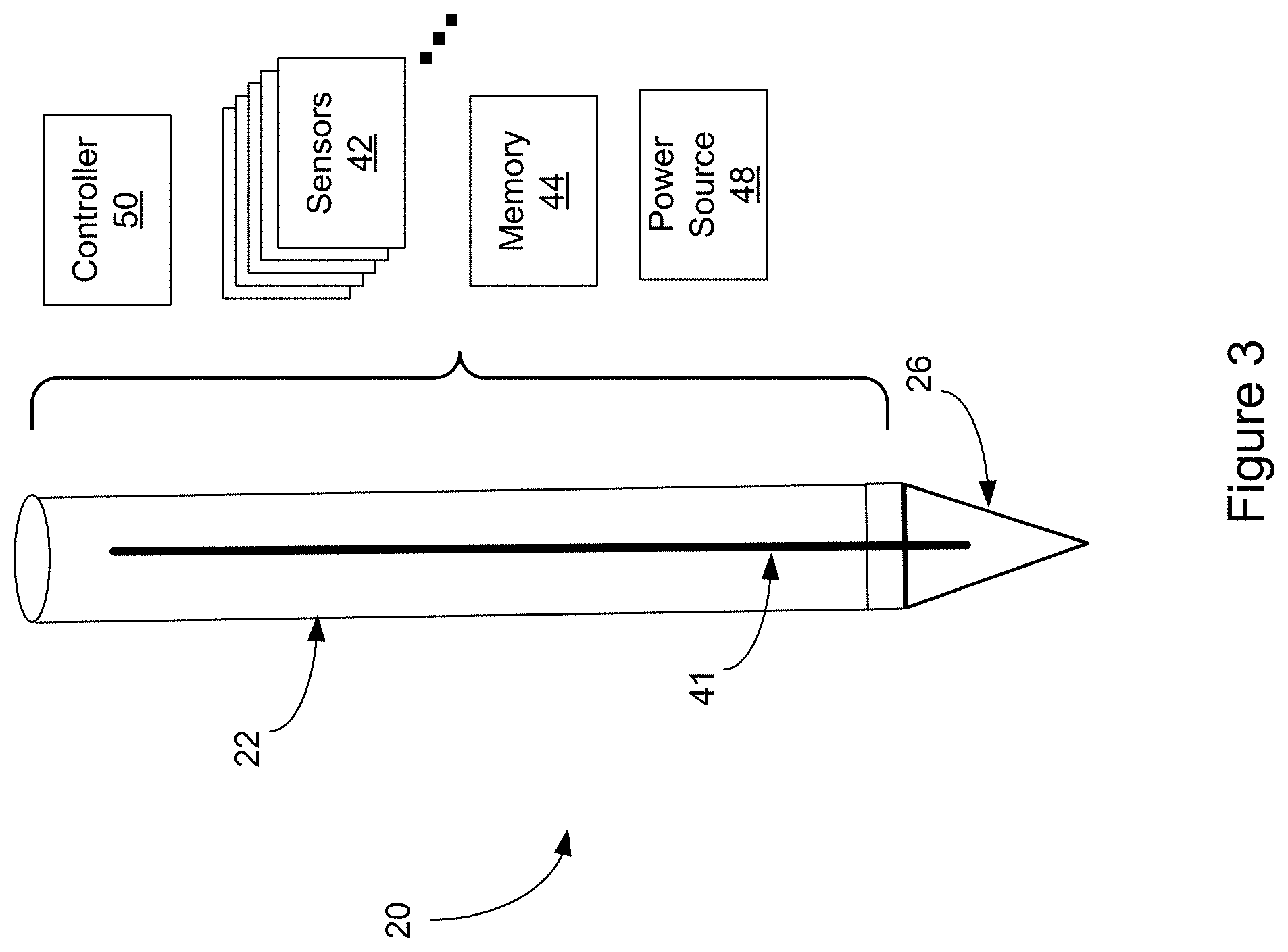
FIG. 3 illustrates example internal components of example active stylus 20. Active stylus 20 includes one or more internal components, such as a controller 50, sensors 42, memory 44, or power source 48. In particular embodiments, one or more internal components may be configured to provide for interaction between active stylus 20 and a user or between a device and a user. In other particular embodiments, one or more internal components, in conjunction with one or more external components described above, may be configured to provide interaction between active stylus 20 and a user or between a device and a user. As an example and not by way of limitation, interactions may include communication between active stylus 20 and a device, enabling or altering functionality of active stylus 20 or a device, or providing feedback to or accepting input from one or more users. As another example, active stylus 20 may communicate via any applicable short distance, low energy data transmission or modulation link, such as, for example and without limitation, via a radio frequency (RF) communication link. In this case, active stylus 20 includes a RF device for transmitting data over the RF link.
Controller 50 may be a microcontroller or any other type of processor suitable for controlling the operation of active stylus 20. Controller 50 may be one or more ICs--such as, for example, general-purpose microprocessors, microcontrollers, PLDs, PLAs, or ASICs. Controller 50 may include a processor unit, a drive unit, a sense unit, and a storage unit. The drive unit may supply signals to electrodes of tip 26 through center shaft 41. The drive unit may also supply signals to control or drive sensors 42 or one or more external components of active stylus 20. The sense unit may sense signals received by electrodes of tip 26 through center shaft 41 and provide measurement signals to the processor unit representing input from a device. The sense unit may also sense signals generated by sensors 42 or one or more external components and provide measurement signals to the processor unit representing input from a user. The processor unit may control the supply of signals to the electrodes of tip 26 and process measurement signals from the sense unit to detect and process input from the device. The processor unit may also process measurement signals from sensors 42 or one or more external components. The storage unit may store programming for execution by the processor unit, including programming for controlling the drive unit to supply signals to the electrodes of tip 26, programming for processing measurement signals from the sense unit corresponding to input from the device, programming for processing measurement signals from sensors 42 or external components to initiate a pre-determined function or gesture to be performed by active stylus 20 or the device, and other suitable programming, where appropriate. As an example and not by way of limitation, programming executed by controller 50 may electronically filter signals received from the sense unit. Although this disclosure describes a particular controller 50 having a particular implementation with particular components, this disclosure contemplates any suitable controller having any suitable implementation with any suitable components.
In particular embodiments, active stylus 20 may include one or more sensors 42, such as touch sensors, gyroscopes, accelerometers, contact sensors, or any other type of sensor that detect or measure data about the environment in which active stylus 20 operates. Sensors 42 may detect and measure one or more characteristic of active stylus 20, such as acceleration or movement, orientation, contact, pressure on outer body 22, force on tip 26, vibration, or any other suitable characteristic of active stylus 20. As an example and not by way of limitation, sensors 42 may be implemented mechanically, electronically, or capacitively. As described above, data detected or measured by sensors 42 communicated to controller 50 may initiate a pre-determined function or gesture to be performed by active stylus 20 or the device. In particular embodiments, data detected or received by sensors 42 may be stored in memory 44. Memory 44 may be any form of memory suitable for storing data in active stylus 20. In other particular embodiments, controller 50 may access data stored in memory 44. As an example and not by way of limitation, memory 44 may store programming for execution by the processor unit of controller 50. As another example, data measured by sensors 42 may be processed by controller 50 and stored in memory 44.
Power source 48 may be any type of stored-energy source, including electrical or chemical-energy sources, suitable for powering the operation of active stylus 20. In particular embodiments, power source 48 may be charged by energy from a user or device. As an example and not by way of limitation, power source 48 may be a rechargeable battery that may be charged by motion induced on active stylus 20. In other particular embodiments, power source 48 of active stylus 20 may provide power to or receive power from the device or other external power source. As an example and not by way of limitation, power may be inductively transferred between power source 48 and a power source of the device or another external power source, such as a wireless power transmitter. Power source may also be powered by a wired connection through an applicable port coupled to a suitable power source.
FIG. 4 illustrates an example active stylus 20 with an example device 52. Device 52 may have a display (not shown) and a touch sensor with a touch-sensitive area 54. Device 52 display may be a liquid crystal display (LCD), a LED display, a LED-backlight LCD, or other suitable display and may be visible though a cover panel and substrate (and the drive and sense electrodes of the touch sensor disposed on it) of device 52. Although this disclosure describes a particular device display and particular display types, this disclosure contemplates any suitable device display and any suitable display types.
Device 52 electronics may provide the functionality of device 52. As example and not by way of limitation, device 52 electronics may include circuitry or other electronics for wireless communication to or from device 52, execute programming on device 52, generating graphical or other user interfaces (UIs) for device 52 display to display to a user, managing power to device 52 from a battery or other power source, taking still pictures, recording video, other suitable functionality, or any suitable combination of these. Although this disclosure describes particular device electronics providing particular functionality of a particular device, this disclosure contemplates any suitable device electronics providing any suitable functionality of any suitable device.
In particular embodiments, active stylus 20 and device 52 may be synchronized prior to communication of data between active stylus 20 and device 52. As an example and not by way of limitation, active stylus 20 may be synchronized to the device through a pre-determined bit sequence transmitted by the touch sensor of device 52. As another example, active stylus 20 may be synchronized to device by processing the drive signal transmitted by drive electrodes of the touch sensor of device 52. Active stylus 20 may interact or communicate with device 52 when active stylus 20 is brought in contact with or in proximity to touch-sensitive area 54 of the touch sensor of device 52. In particular embodiments, interaction between active stylus 20 and device 52 may be capacitive or inductive. As an example and not by way of limitation, when active stylus 20 is brought in contact with or in the proximity of touch-sensitive area 54 of device 52, signals generated by active stylus 20 may influence capacitive nodes of touch-sensitive area of device 52 or vice versa. As another example, a power source of active stylus 20 may be inductively charged through the touch sensor of device 52, or vice versa. Although this disclosure describes particular interactions and communications between active stylus 20 and device 52, this disclosure contemplates any suitable interactions and communications through any suitable means, such as mechanical forces, current, voltage, or electromagnetic fields.
In particular embodiments, measurement signal from the sensors of active stylus 20 may initiate, provide for, or terminate interactions between active stylus 20 and one or more devices 52 or one or more users, as described above. Interaction between active stylus 20 and device 52 may occur when active stylus 20 is contacting or in proximity to device 52. As an example and not by way of limitation, a user may perform a gesture or sequence of gestures, such as shaking or inverting active stylus 20, whilst active stylus 20 is hovering above touch-sensitive area 54 of device 52. Active stylus may interact with device 52 based on the gesture performed with active stylus 20 to initiate a pre-determined function, such as authenticating a user associated with active stylus 20 or device 52. Although this disclosure describes particular movements providing particular types of interactions between active stylus 20 and device 52, this disclosure contemplates any suitable movement influencing any suitable interaction in any suitable way.
Active stylus 20 may include one or more electrodes configured to communicate data between active stylus 20 and one or more devices 52 or other active styluses. By way of example and without limitation, the electrodes of active stylus 20 may reside on outer body 22 of active stylus, in active stylus tip 26, or on or in any other suitable part of active stylus 20.
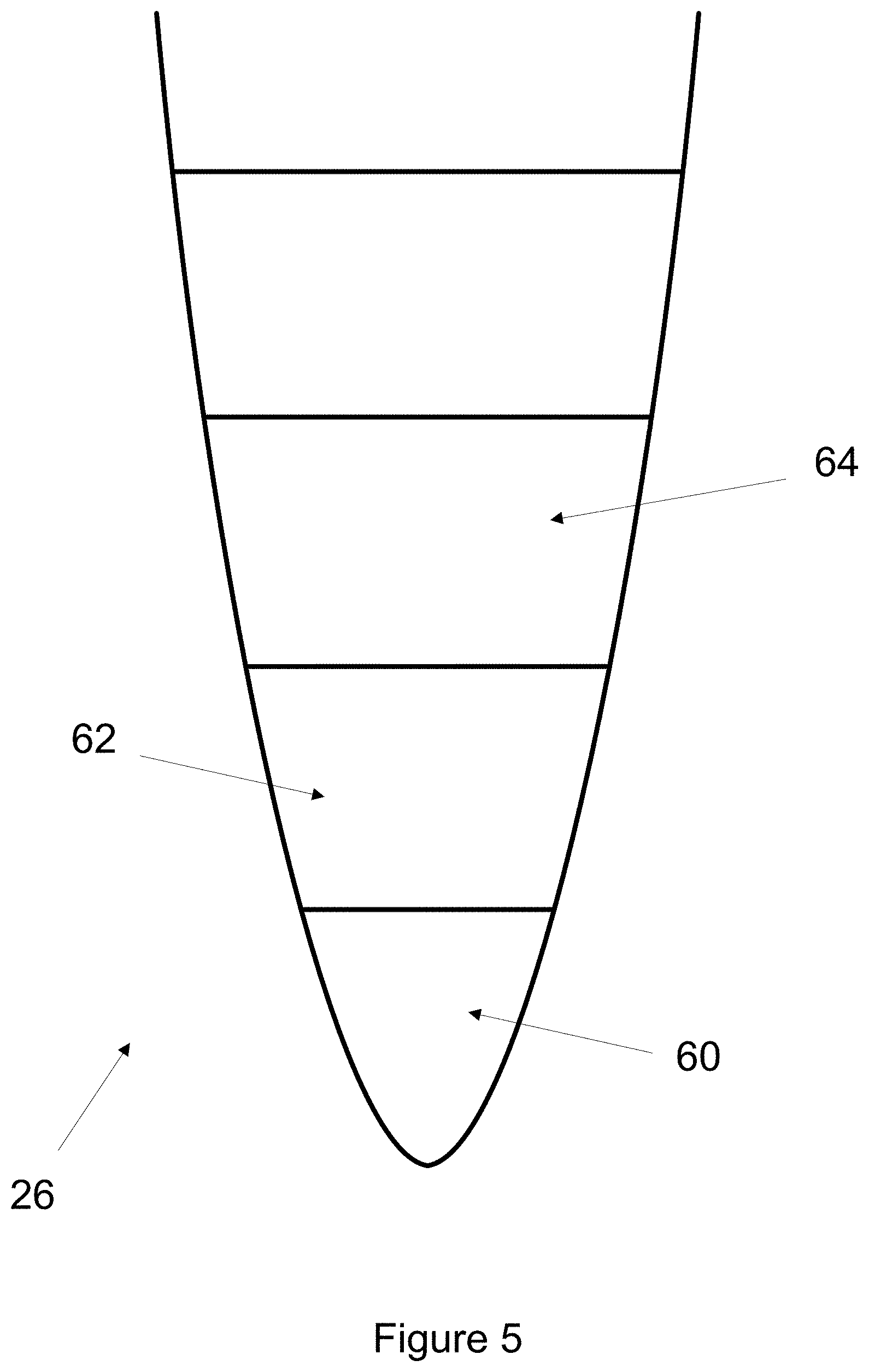
FIG. 5 illustrates an embodiment of active stylus 20, by way of example and without limitation, with electrodes in active stylus tip 26. Active stylus tip 26 may include one or more electrodes 60, 62, and 64 configured to communicate data between active stylus 20 and one or more devices or other active styluses. Active stylus tip 26 may include further components or functionality not illustrated in FIG. 5 or the following figures. In other embodiments, electrodes in active stylus 20 may not reside in active stylus tip 26 or may not reside solely in active stylus tip 26.
As an example and without limitation, one or more electrodes in active stylus 20 may be a ground electrode, a guard electrode, a drive electrode, or a sense electrode. The electrodes in active stylus 20 may each be an area of conductive material forming a shape, such as, for example, a disc, square, rectangle, other suitable shapes, or suitable combination of these. One or more cuts in one or more layers of conductive material may (at least in part) create the shape of an electrode, and the area of the shape may (at least in part) be bounded by those cuts. In particular embodiments, the conductive material of an electrode may occupy approximately 100% of the area of its shape. As an example and not by way of limitation, an electrode may be made of indium tin oxide (ITO) and the ITO of the electrode may occupy approximately 100% of the area of its shape, where appropriate. In particular embodiments, the conductive material of an electrode may occupy substantially less than 100% of the area of its shape. As an example and not by way of limitation, an electrode may be made of fine lines of metal or other conductive material (such as, for example, copper, silver, or a copper- or silver-based material) and the fine lines of conductive material may occupy substantially less than 100% of the area of its shape in a hatched, mesh, or other suitable patterns. Although this disclosure describes or illustrates particular electrodes made of particular conductive material forming particular shapes with particular fills having particular patterns, this disclosure contemplates any suitable electrodes made of any suitable conductive material forming any suitable shapes with any suitable fills having any suitable patterns. Where appropriate, the shapes of the electrodes (or other elements) of the active stylus 20 may constitute in whole or in part one or more macro-features of the active stylus 20. One or more characteristics of the implementation of those shapes (such as, for example, the conductive materials, fills, or patterns within the shapes) may constitute in whole or in part one or more micro-features of the active stylus 20. One or more macro-features of an active stylus 20 may determine one or more characteristics of its functionality, and one or more micro-features of the active stylus 20 may determine one or more optical features of the active stylus 20, such as transmittance, refraction, or reflection.
The multiple electrodes of active stylus 20 may each be able to receive signals from or send signals to other components of active stylus 20, a user, or device 52, without limitation. In particular embodiments, including those illustrated in FIG. 5, the electrodes of active stylus 20 (in FIG. 5, the electrodes residing in active stylus tip 26) may each receive and send signals via center shaft 41. As an example, the electrodes in active stylus 20 may each receive signals from controller 50 via center shaft 41. In particular embodiments, a drive unit in controller 50 may supply signals to each of the electrodes in active stylus 20 via center shaft 41. The multiple electrodes of active stylus 20 may also each send signals to controller 50 via center shaft 41. As an example, the electrodes in active stylus 20 may each send signals to a sense unit in controller 50 via center shaft 41. In other embodiments, a processor in controller 50 may control the operation of the electrodes in active stylus 20, either via drive or sense units or directly. The electrodes of active stylus 20 may send or receive signals in any suitable manner, whether via center shaft 41 or other channels of communication.
Active stylus 20 may encounter noise when receiving or transmitting signals. As examples, noise may be introduced into the received or transmitted signals from data quantization, limitations of position-calculation algorithms, bandwidth limitations of measurement hardware, accuracy limitations of analog front ends of devices with which active stylus 20 communicates, the physical layout of the system, sensor noise, charger noise, device noise, stylus circuitry noise, or external noise. The noise external to active stylus 20 is often omnidirectional and may be modeled as white noise, and, in specific cases, Gaussian white noise.
The use of differential sensing may alleviate the issues caused by noise in the transmission or reception of signals by active stylus 20. Differential sensing, in particular embodiments, is the comparison of signals received by multiple electrodes, and it may be used to boost the signal-to-noise ratio (SNR) of the overall received signal at active stylus 20.
If a signal of interest S is coming from device 52, then each electrode in the sensing mode in active stylus 20 will sense some version of S. With reference to FIG. 5, each electrode, including electrodes 60, 62, and 64, may sense some version of the signal S being transmitted by device 52. The version of signal S sensed at electrode 60 will be denoted S_60, the version sensed at electrode 62 will be denoted S_62, and the version sensed at electrode 64 will be denoted S_64. The actual received signal at each of these electrodes, however, will also have external noise N as a component. In many cases, external noise N will have identical statistical characteristics at each electrode. Thus, what is actually received at electrode 60 will be S_60+N, what is actually received at electrode 62 will be S_62+N, and what is actually received at electrode 64 will be S_64+N.
In order to remove the unwanted effects of noise, differential sensing may be employed by comparing at least two signals received by two different electrodes. The signals received from any two electrodes capable of sensing signals may be compared. As an example, and not by way of limitation, the signals received from electrodes 60 and 64 may be compared. This comparison may be done by subtracting the signal received by electrode 64 from the signal received by electrode 60. This would yield the following equation for the resulting output of the comparator: (S_60+N)-(S_64+N). The final result would, therefore, be S_60-S_64.
If either S_60 or S_64 are known quantities, then the other, unknown, quantity may be determined from the output of the comparator. That is, if electrode 64, for example, is a reference electrode, such that the signal S_64 is a reliable or known quantity (including, for example, a signal having a steady value of 0 before being added to noise N), then effects of noise N in this system may be removed through the use of differential sensing. In the above example, the signal of interest coming from electrode 60, S_60, may be computed as the output of the comparison plus S_64, which is a known value. This allows for the signal received at active stylus 20 to be more accurate. In certain embodiments, it may be desirable that the reference electrode used for differential sensing have a reliable or known reference signal value and also be placed within active stylus 20 such that the noise received at the reference electrode is statistically the same as the noise received at the non-reference electrodes. As an example, if it is desired that the reference electrode have a reference signal value of 0, reference electrode should be placed on active stylus 20 such that it receives as little of the signal S transmitted by device 52 as possible, but still receives noise signal N received by the other electrodes. As another example, if it is desired that the reference electrode have a reference signal value of S_ref, the electrode should be placed on active stylus 20 such that it receives S_ref (from a signal source on active stylus 20, for example) reliably but also receives noise signal N received by the other electrodes.
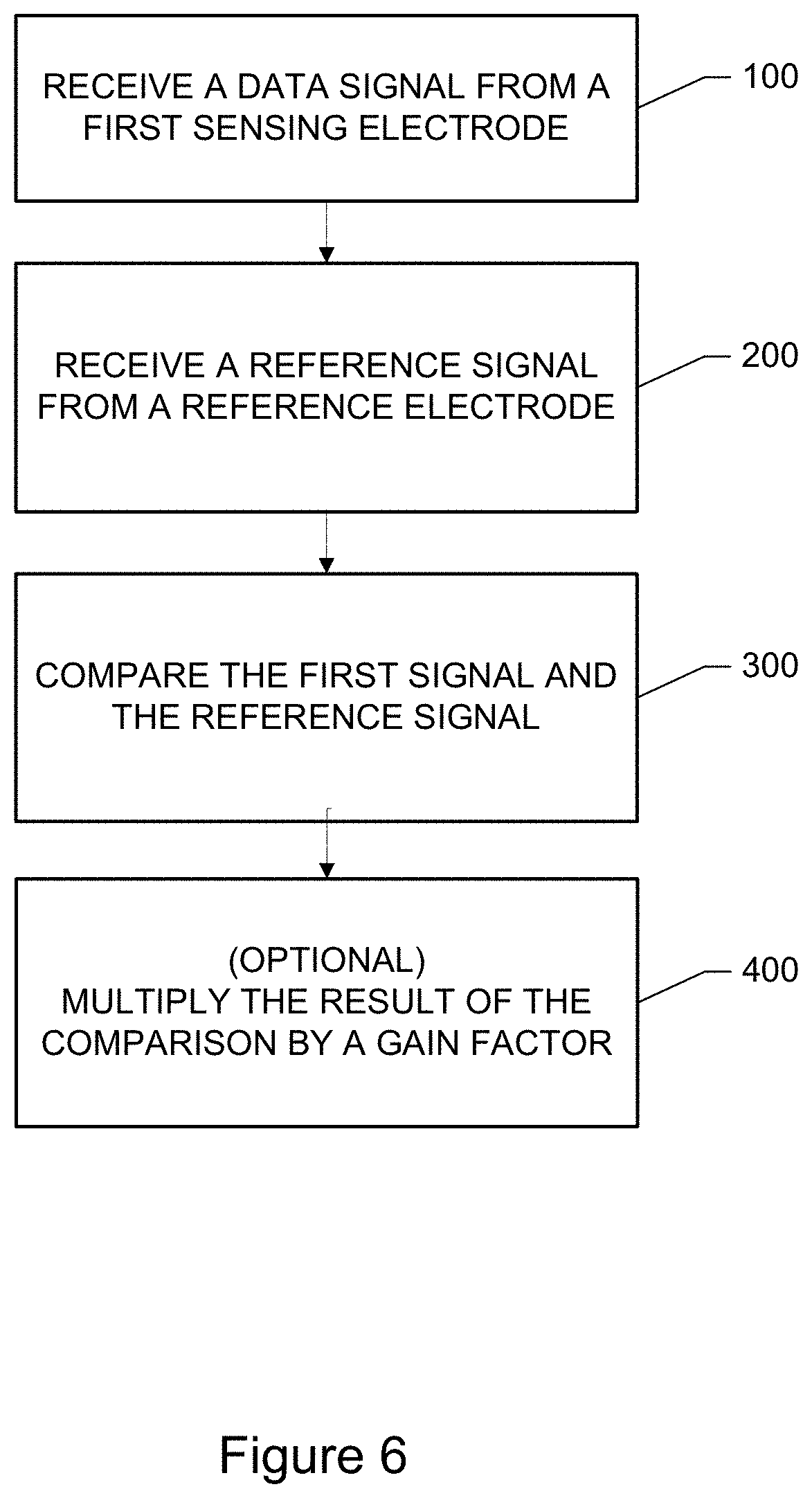
In particular embodiments, the comparator used for differential sensing is an analog comparator, including, for example, an operational amplifier (op-amp), with one input to the op-amp coming from one electrode, and another input to the op-amp coming from a different electrode in active stylus 20. In other embodiments, other analog comparators may be employed. In yet other embodiments, the comparator used for differential sensing is a digital comparator, including, for example, a dedicated voltage comparator chip. The comparator, whether digital or analog, may also, in particular embodiments, multiply the resulting signal by a gain. In particular embodiments, differential sensing may occur with respect to a common ground within active stylus 20.
The comparator may reside in controller 50 of active stylus 20. In particular embodiments, the comparator is part of the sense unit in controller 50. In yet other embodiments, the comparator is part of the processor in controller 50. Although this disclosure describes the comparator residing in controller 50, this disclosure contemplates any suitable location within active stylus 20 for the comparator.
FIG. 6 illustrates an example method for differential sensing. The method may start at step 100, where a comparator receives a data signal from a first sensing electrode. At step 200, the comparator receives a reference signal from a reference electrode. At step 300, the comparator compares the first signal and the reference signal. As discussed above, in particular embodiments, this comparison involves the subtraction of the reference signal from the first signal. In certain embodiments, at step 400, the comparator optionally multiplies the result of the comparison by a gain factor, at which point the method may end. In particular embodiments, this gain factor may simply be 1, such that no amplification results. Particular embodiments may repeat the steps of the method of FIG. 6, where appropriate. Moreover, although this disclosure describes and illustrates particular steps of the method of FIG. 6 as occurring in a particular order, this disclosure contemplates any suitable steps of the method of FIG. 6 occurring in any suitable order. Furthermore, although this disclosure describes and illustrates particular components, devices, or systems carrying out particular steps of the method of FIG. 6, this disclosure contemplates any suitable combination of any suitable components, devices, or systems carrying out any suitable steps of the method of FIG. 6.
Herein, reference to a computer-readable non-transitory storage medium encompasses a semiconductor-based or other integrated circuit (IC) (such, as for example, a field-programmable gate array (FPGA) or an application-specific IC (ASIC)), a hard disk, an HDD, a hybrid hard drive (HHD), an optical disc, an optical disc drive (ODD), a magneto-optical disc, a magneto-optical drive, a floppy disk, a floppy disk drive (FDD), magnetic tape, a holographic storage medium, a solid-state drive (SSD), a RAM-drive, a SECURE DIGITAL card, a SECURE DIGITAL drive, another suitable computer-readable non-transitory storage medium or a combination of two or more of these, where appropriate. A computer-readable non-transitory storage medium may be volatile, non-volatile, or a combination of volatile and non-volatile, where appropriate. Herein, "or" is inclusive and not exclusive, unless expressly indicated otherwise or indicated otherwise by context. Therefore, herein, "A or B" means "A, B, or both," unless expressly indicated otherwise or indicated otherwise by context. Moreover, "and" is both joint and several, unless expressly indicated otherwise or indicated otherwise by context. Therefore, herein, "A and B" means "A and B, jointly or severally," unless expressly indicated otherwise or indicated otherwise by context.
This disclosure encompasses all changes, substitutions, variations, alterations, and modifications to the example embodiments herein that a person having ordinary skill in the art would comprehend. Moreover, reference in the appended claims to an apparatus or system or a component of an apparatus or system being adapted to, arranged to, capable of, configured to, enabled to, operable to, or operative to perform a particular function encompasses that apparatus, system, component, whether or not it or that particular function is activated, turned on, or unlocked, as long as that apparatus, system, or component is so adapted, arranged, capable, configured, enabled, operable, or operative.
* * * * *
D00000
D00001
D00002
D00003
D00004
D00005
D00006
XML
uspto.report is an independent third-party trademark research tool that is not affiliated, endorsed, or sponsored by the United States Patent and Trademark Office (USPTO) or any other governmental organization. The information provided by uspto.report is based on publicly available data at the time of writing and is intended for informational purposes only.
While we strive to provide accurate and up-to-date information, we do not guarantee the accuracy, completeness, reliability, or suitability of the information displayed on this site. The use of this site is at your own risk. Any reliance you place on such information is therefore strictly at your own risk.
All official trademark data, including owner information, should be verified by visiting the official USPTO website at www.uspto.gov. This site is not intended to replace professional legal advice and should not be used as a substitute for consulting with a legal professional who is knowledgeable about trademark law.