Circuits and methods for measuring the output current of a switched capacitor regulator
Meyvaert , et al.
U.S. patent number 10,720,832 [Application Number 16/264,079] was granted by the patent office on 2020-07-21 for circuits and methods for measuring the output current of a switched capacitor regulator. This patent grant is currently assigned to Lion Semiconductor Inc.. The grantee listed for this patent is Lion Semiconductor Inc.. Invention is credited to Fred Chen, John Crossley, Thomas Li, Zhipeng Li, Hans Meyvaert, Bertram J. Rodgers.


| United States Patent | 10,720,832 |
| Meyvaert , et al. | July 21, 2020 |
Circuits and methods for measuring the output current of a switched capacitor regulator
Abstract
Circuits comprising: a capacitor; switches that, when State0, couple the capacitor in parallel with the load and, when State1, couple the capacitor in series with the load, wherein a first of the switches connects the capacitor to ground when in State0 and wherein a second of the switches connects the capacitor to an input voltage when in State1; a third switch, wherein a first side of the third switch is connected to the capacitor identically to one of the first switch and the second switch (OFWSW), wherein the third switch switches identically to the OFWSW, wherein the third switch is smaller than the OFWSW; a first resistor connected to the second side of the third switch; and a hardware processor that measures a current flowing through the first resistor and estimates the current provided to the load based on the current measured as flowing through the first resistor.
| Inventors: | Meyvaert; Hans (Oakland, CA), Li; Thomas (Mountain View, CA), Chen; Fred (Oakland, CA), Crossley; John (Oakland, CA), Li; Zhipeng (Fremont, CA), Rodgers; Bertram J. (San Francisco, CA) | ||||||||||
|---|---|---|---|---|---|---|---|---|---|---|---|
| Applicant: |
|
||||||||||
| Assignee: | Lion Semiconductor Inc. (San
Francisco, CA) |
||||||||||
| Family ID: | 70459051 | ||||||||||
| Appl. No.: | 16/264,079 | ||||||||||
| Filed: | January 31, 2019 |
Prior Publication Data
| Document Identifier | Publication Date | |
|---|---|---|
| US 20200144908 A1 | May 7, 2020 | |
Related U.S. Patent Documents
| Application Number | Filing Date | Patent Number | Issue Date | ||
|---|---|---|---|---|---|
| 62756064 | Nov 5, 2018 | ||||
| Current U.S. Class: | 1/1 |
| Current CPC Class: | H02M 3/158 (20130101); H02M 3/07 (20130101); H02M 1/00 (20130101); H02M 2001/0054 (20130101); H02M 2001/0009 (20130101) |
| Current International Class: | H02M 3/07 (20060101); H02M 1/00 (20060101); H02M 7/483 (20070101); H02M 3/158 (20060101) |
| Field of Search: | ;323/272 |
References Cited [Referenced By]
U.S. Patent Documents
| 7068094 | June 2006 | Jamal |
| 9653990 | May 2017 | Wang |
| 2007/0176671 | August 2007 | Ishida |
| 2008/0122522 | May 2008 | Nagasawa |
| 2011/0018511 | January 2011 | Carpenter |
| 2012/0224288 | September 2012 | Uota |
| 2013/0249512 | September 2013 | Saito |
| 2013/0300385 | November 2013 | Li |
| 2016/0054749 | February 2016 | Fujiwara |
| 2016/0211739 | July 2016 | Hissink |
| 2016/0315539 | October 2016 | Lee |
| 2018/0006643 | January 2018 | Schulmeyer |
| 2018/0054121 | February 2018 | Chen |
| 2018/0123452 | May 2018 | Meyvaert |
| 2019/0006933 | January 2019 | Lidsky |
Other References
|
International Search Report and Written Opinion dated Nov. 20, 2019 in International Patent Application No. PCT/US2019/057659. cited by applicant. |
Primary Examiner: Tran; Thienvu V
Assistant Examiner: Tiku; Sisay G
Attorney, Agent or Firm: Byrne Poh LLP
Parent Case Text
CROSS-REFERENCE TO RELATED APPLICATION
This application claims the benefit of U.S. Provisional Patent Application No. 62/756,064, filed Nov. 5, 2018, which is hereby incorporated by reference herein in its entirety.
Claims
What is claimed is:
1. A circuit for measuring a current provided to a load comprising a capacitor having a first side and a second side; a plurality of switches that, when in a first state, couple the capacitor in parallel with the load and, when in a second state, couple the capacitor in series with the load, wherein a first switch of the plurality of switches has a first side, a second side, and a control input and connects the first side of the capacitor to ground when the plurality of switches are in the first state and wherein a second switch of the plurality of switches has a first side, a second side, and a control input and connects the second side of the capacitor to an input voltage when the plurality of switches are in the second state; a third switch having a first side, a second side, and a control input, wherein the first side of the third switch is connected to the first side of one of the first switch and the second switch, wherein the control input of the third switch is connected to the control input of the one of the first switch and the second switch, and wherein the third switch is smaller than the one of the first switch and the second switch; a first resistor having a first side and a second side, wherein the first side of the first resistor is directly connected to the second side of the third switch; and a hardware processor that measures a current flowing through the first resistor and estimates the current provided to the load based on the current measured as flowing through the first resistor.
2. The circuit for measuring a current provided to a load of claim 1, wherein the one of the first switch and the second switch is the first switch.
3. The circuit for measuring a current provided to a load of claim 2, wherein the first switch and the third switch are NMOS transistors and wherein the second switch is a PMOS transistor.
4. The circuit for measuring a current provided to a load of claim 2, wherein the second side of the resistor is connected to ground.
5. The circuit for measuring a current provided to a load of claim 1, wherein the one of the first switch and the second switch is the second switch.
6. The circuit for measuring a current provided to a load of claim 5, wherein the second switch and the third switch are PMOS transistors and wherein the first switch is an NMOS transistor.
7. The circuit for measuring a current provided to a load of claim 5, wherein the second side of the resistor is connected to the input voltage.
8. The circuit for measuring a current provided to a load of claim 5, further comprising: a fourth switch having a first side, a second side, and a control input, wherein the first side of the fourth switch is connected to the first side of the first switch, wherein the control input of the fourth switch is connected to the control input of the first switch, and wherein the fourth switch is smaller than the first switch; and a second resistor having a first side and a second side, wherein the first side of the second resistor is connected to the second side the fourth switch and wherein the second side of the second resistor is connected to ground, wherein the hardware processor also measures a current flowing through the second resistor and estimates the current provided to the load based on the current measured as flowing through the second resistor.
9. The circuit for measuring a current provided to a load of claim 8, wherein the hardware processor estimates the current provided to the load based on a combination of the current flowing through the first resistor and the current flowing through the second resistor.
10. The circuit for measuring a current provided to a load of claim 1, wherein the third switch has a width that is equal to or smaller than 1/10th of a width of the one of the first switch and the second switch.
11. The circuit for measuring a current provided to a load of claim 1, wherein the third switch has a width that is equal to or smaller than 1/100th of a width of the one of the first switch and the second switch.
12. The circuit for measuring a current provided to a load of claim 1, wherein the third switch has a width that is equal to or smaller than 1/1000th of a width of the one of the first switch and the second switch.
13. The circuit for measuring a current provided to a load of claim 1, further comprising an analog-to-digital converter that measures a voltage at the first side of the first resistor.
14. The circuit for measuring a current provided to a load of claim 1, wherein the hardware processor measures the current flowing through the first resistor by determining a voltage across the resistor and dividing the voltage across the resistor by a known value of the resistor.
15. The circuit for measuring a current provided to a load of claim 1, wherein the hardware processor estimates the current provided to the load by dividing the current flowing through the first resistor by a percentage of time that the plurality of switches are in the first state when the one of the first switch and the second switch is the first switch and by a percentage of time that the plurality of switches are in the second state when the one of the first switch and the second switch is the second switch.
Description
BACKGROUND
Switched Capacitor (SC) regulators can be used in various applications including direct-current-to-direct-current (DC/DC) converters and battery charger integrated circuits (ICs).
It can be helpful to measure the output current of a Switched Capacitor (SC) regulator. For example, it can be helpful to measure the output current of an SC battery charger IC so that the SC battery charger IC can regulate a charge current used to charge a battery. To regulate the charge current, the charger IC needs to measure its output current and determine if it is larger or smaller than a target output current value. Based on that result, the charger IC can adjust the output current to be as similar as possible to the target value. In another example, it can be helpful to measure output power in a SC DC/DC converter by measuring output current and multiplying it by an output voltage. In a power management IC (PMIC) with multiple SC DC/DC converters, it can be helpful to measure the output power of each SC DC/DC converter so that the PMIC can keep track of how much power is consumed by each DC/DC converter.
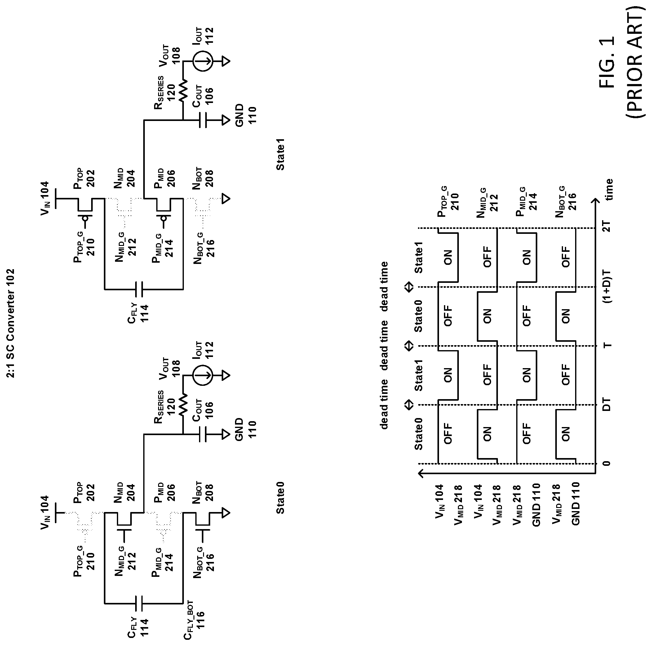
While it is useful to measure output current, prior techniques for doing so are inefficient from a power usage perspective. A straightforward way to measure output current is to add a series resistor at the output and measure the voltage across the resistor as illustrated in FIG. 1. Since IR=V, measuring the voltage across the resistor R.sub.SERIES 120 and dividing by the resistor value can compute the amount of current flowing through R.sub.SERIES 120. The problem with this approach is that there is power loss of I.sup.2R. If R is equal to 5 milliOhms and I is equal to 5 Amps, I.sup.2R power loss is equal to 125 milliWatts. It is possible to reduce R to reduce I.sup.2R loss. However, a small R value results in a small IR=V value, and it becomes more difficult to sense the small voltage value (e.g., a higher bit analog to digital converter is needed to sense smaller voltages).
Accordingly, new mechanisms (which can include circuits and methods) for measuring the output current of a switched capacitor (SC) regulator are desirable.
SUMMARY
Circuits and methods for measuring the output current of a switched capacitor regulator are provided. In some embodiments, circuits for measuring a current provided to a load comprising: a capacitor having a first side and a second side; a plurality of switches that, when in a first state, couple the capacitor in parallel with the load and, when in a second state, coupled the capacitor in series with the load, wherein a first switch of the plurality of switches connects the first side of the capacitor to ground when the plurality of switches are in the first state and wherein a second switch of the plurality of switches connects the second side of the capacitor to an input voltage when the plurality of switches are in the second state; a third switch having a first side and a second side, wherein the first side of the third switch is connected to the capacitor identically to one of the first switch and the second switch, wherein the third switch switches identically to the one of the first switch and the second switch, wherein the third switch is smaller than the one of the first switch and the second switch; a first resistor having a first side and a second side, wherein the first side of the first resistor is connected to the second side the third switch; and a hardware processor that measures a current flowing through the first resistor and estimates the current provided to the load based on the current measured as flowing through the first resistor.
BRIEF DESCRIPTION OF THE DRAWINGS
FIG. 1 is schematic diagram of an example of a switched capacitor converter in accordance with the prior art.
FIG. 2 is schematic diagram of an example of a switched capacitor converter using a small switch and a small resistor to estimate output current in accordance with some embodiments.
FIG. 3 is schematic diagram of another example of a switched capacitor converter using a small switch and a small resistor to estimate output current in accordance with some embodiments.
FIG. 4 is schematic diagram of an example of a switched capacitor converter using a replica converter to estimate output current in accordance with some embodiments.
DETAILED DESCRIPTION
Mechanisms (which can include circuits and methods) for measuring the output current of a switched capacitor (SC) regulator are provided.
In some embodiments, the mechanisms can measure the output current of a SC regulator by measuring input current (I.sub.IN) to the SC regulator, measuring the output voltage (V.sub.OUT) of the SC regulator, measuring the input voltage (V.sub.IN) to the SC regulator, and calculating the output current (I.sub.OUT) based on these measurements and an efficiency estimate.
For example, in some embodiments, the efficiency estimate can be calculated during a calibration process using the following equation: Efficiency=P.sub.OUT/P.sub.IN=(V.sub.OUT.times.I.sub.OUT)/(V.sub.IN.times- .I.sub.IN). where V.sub.IN, V.sub.OUT, I.sub.IN, and I.sub.OUT are measured under expected operating conditions. Then, during operation, I.sub.OUT can be calculated using the following equation: I.sub.OUT=Efficiency.times.(V.sub.IN.times.I.sub.IN)/V.sub.OUT.
In some embodiments, efficiency can be estimated using pre-simulated data and stored in memory in an SC regulator integrated circuit (IC) or in external memory. V.sub.IN and V.sub.OUT can be measured in any suitable manner, such as using an analog to digital converter (ADC), for example. In some cases, V.sub.IN and V.sub.OUT values need not be measured when set to given values by an SC regulator, for example. I.sub.IN can be determined by measuring the voltage across a resistor in series with V.sub.IN (which can be done in any suitable manner, such as using an ADC) and calculating for the current passing through that resistor (as described above). While this technique will incur an I.sup.2R loss in the resistor, the I.sup.2R loss of measuring I.sub.IN using a resistor is smaller than the I.sup.2R loss of measuring I.sub.OUT when I.sub.IN is smaller than I.sub.OUT. For example, in a 2:1 SC regulator, the input current is roughly 50% of the output current, so I.sup.2R loss when I.sub.IN is measured is roughly 25% of the I.sup.2R loss when I.sub.OUT is measured. An advantage of measuring I.sub.OUT in this manner is that it is less lossy to measure I.sub.IN, V.sub.OUT, and V.sub.IN and use an estimate efficiency to calculate I.sub.OUT than to measure I.sub.OUT as shown in FIG. 1. A disadvantage of measuring I.sub.OUT in this manner is that it is less accurate than measuring I.sub.OUT directly using a series resistor at the output of the SC regulator (as shown in FIG. 1) because errors in the efficiency estimate and the measurements of V.sub.IN, I.sub.IN, V.sub.OUT can compound.
In some embodiments, the mechanisms can measure the output current of a SC regulator by measuring the output impedance (R.sub.OUT) of the SC regulator and calculate I.sub.OUT. For example, in a N:M SC regulator, the following equation computes I.sub.OUT: I.sub.OUT=(V.sub.IN.times.M/N-V.sub.OUT)/R.sub.OUT. M and N are known based on the SC regulator design, and V.sub.IN and V.sub.OUT can be measured using an ADC in some embodiments. R.sub.OUT is a function of the SC regulator topology (e.g., the values of N and M in the N:M SC regulator), switch on-state resistance (because switches are non-ideal and have parasitic resistance even when they are ON), the switching frequency of the SC regulator (freq), and the amount of flying capacitance (C.sub.FLY). Thus, R.sub.OUT can be represented by: R.sub.OUT=f(topology,R.sub.SWITCH,freq,C.sub.FLY) Among these variables, topology and C.sub.FLY are known since they are decided by the designer in design time. In some embodiments, freq can be measured in any suitable manner (e.g., using counters to count how quickly the signals switch). In some embodiments, R.sub.SWITCH can be measured in any suitable manner (e.g., during calibration by flowing a known current through the switch and measuring the voltage across the switch). The calculated R.sub.SWITCH value can be stored in in a memory, whether it is in the SC regulator chip or external memory, in some embodiments. An advantage of this method of calculating I.sub.OUT is that it does not incur the I.sup.2R loss of using a series resistor. A disadvantage is that it can be less accurate if errors in measuring these variables compound.
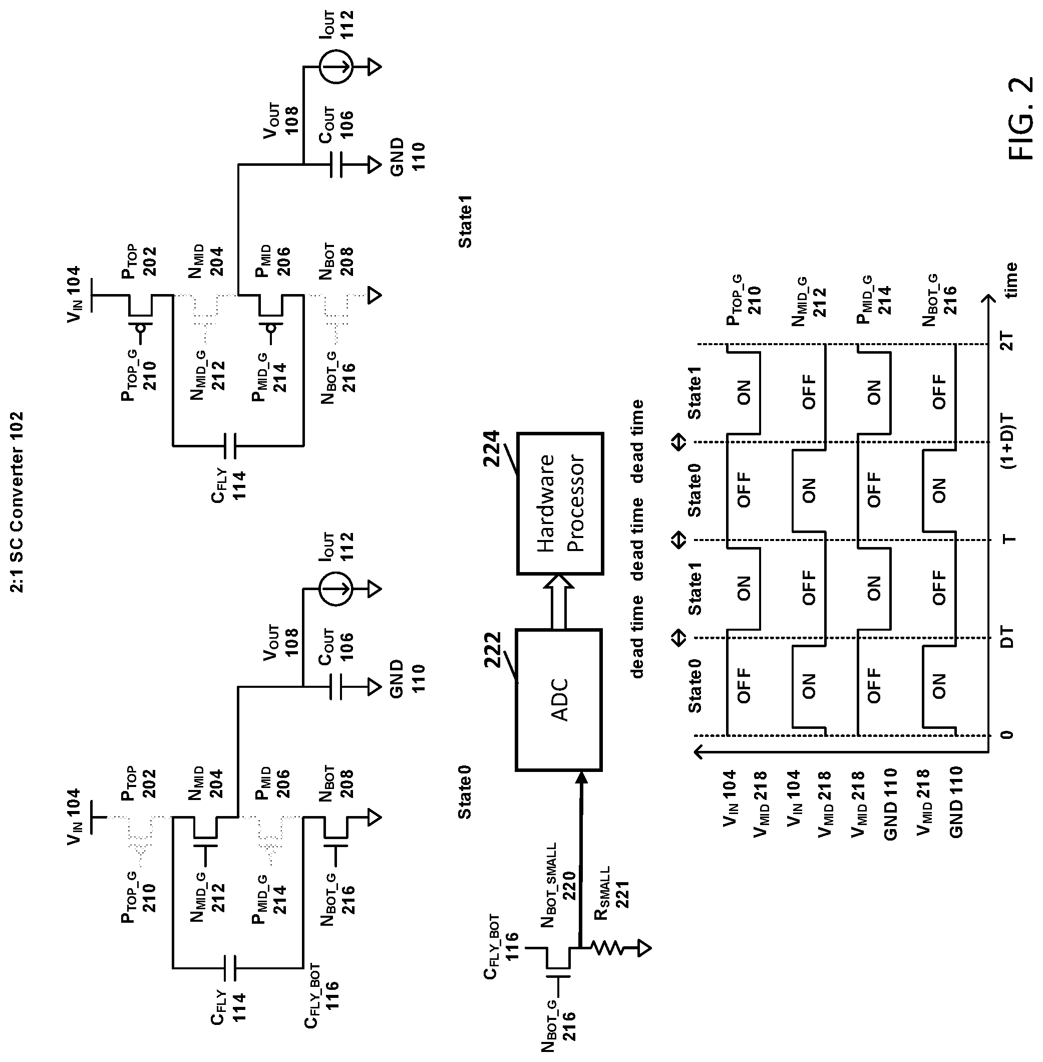
In some embodiments, the mechanisms can measure the output current of a SC regulator by adding a small switch and a series small resistor in parallel with a switch of the SC regulator and using that small resistor to estimate the output current of the SC regulator.
FIG. 2 illustrates an example of a 2:1 SC regulator using this technique on N.sub.BOT 208 in accordance with some embodiments. As shown, a small switch N.sub.BOT_SMALL 220 (with similar characteristics to N.sub.BOT 208 except that it has a much smaller width than N.sub.BOT 208) and a small resistor R.sub.SMALL 221 are connected in parallel to N.sub.BOT 208. That is, the gate of switch N.sub.BOT_SMALL 220 is connected to N.sub.BOT_G 216, the top of N.sub.BOT_SMALL 220 is connected to node C.sub.FLY BOT 116, and the bottom of N.sub.BOT_SMALL 220 is connected via resistor R.sub.SMALL 221 to ground. For example, if the width of N.sub.BOT_SMALL 220 is 1/1000 of the width of N.sub.BOT 208, the current flowing through N.sub.BOT_SMALL 220 is also roughly 1/1000 of the current flowing through N.sub.BOT 208. Once the current value is reduced, it is easier to measure the current with smaller loss. For example, the I.sup.2R loss through R.sub.SMALL would be 1/1,000,000 compared to using a series resistor on N.sub.BOT 208.
During operation, the current through N.sub.BOT 208 can be measured by measuring the voltage across R.sub.SMALL 221 and dividing that by the value of R.sub.SMALL 221 to measure the current through N.sub.BOT_SMALL 220, and then by multiplying the resulting value by 1000 if N.sub.BOT 208 has 1000 times larger width than N.sub.BOT_SMALL 220. If the 2:1 SC regulator is operating at 50% duty cycle, I.sub.OUT 112 can be estimated to be roughly two times the current through N.sub.BOT 208. The voltage can be measured in any suitable manner such as using an analog-to-digital converter (ADC) 222 that is coupled to a hardware processor 224.
Although resistor R.sub.SMALL 221 is shown in FIG. 2 on the lower side of switch N.sub.BOT_SMALL 220, the resistor can instead be placed on the upper side of switch N.sub.BOT_SMALL 220 in some embodiments.
FIG. 3 illustrates an example of a 2:1 SC regulator using this technique on P.sub.TOP 202 in accordance with some embodiments. As shown, a small switch P.sub.TOP_SMALL 320 (with similar characteristics to P.sub.TOP 202 except that it has a much smaller width than P.sub.TOP 202) and a small resistor R.sub.SMALL 321 are connected in parallel to P.sub.TOP 202. That is, the gate of switch P.sub.TOP_SMALL 320 is connected to P.sub.TOP G 210, the top of P.sub.TOP SMALL 320 is connected via resistor R.sub.SMALL 321 to V.sub.IN 104, and the bottom of P.sub.TOP SMALL 320 is connected to node C.sub.FLY TOP 118. Similar to N.sub.BOT_SMALL 220 for N.sub.BOT 208, the width of P.sub.TOP SMALL 320 can be, for example, 1/1000 the width of P.sub.TOP 202. If the 2:1 SC regulator is operating at 50% duty cycle, we can estimate that Tour 112 is roughly two times the current through P.sub.TOP 202. The voltage can be measured in any suitable manner such as using an analog-to-digital converter (ADC) 222 that is coupled to a hardware processor 224.
To calculate I.sub.OUT 112 more accurately, some embodiments can implement both N.sub.BOT_SMALL 220 and R.sub.SMALL 221 and P.sub.TOP_SMALL 320 and R.sub.SMALL 321. Instead of assuming the current in State0 and State1 are equal when duty cycle is 50%, the current flowing in both State0 and State1 can be calculated using N.sub.BOT_SMALL 220 and R.sub.SMALL 221 and P.sub.TOP_SMALL 320 and R.sub.SMALL 321, respectively, and adding the two current values results in I.sub.OUT 112.
Although resistor R.sub.SMALL 321 is shown in FIG. 3 on the upper side of switch P.sub.TOP_SMALL 320, the resistor can instead be placed on the lower side of switch P.sub.TOP_SMALL 320 in some embodiments.
In some embodiments, when using multi-phase SC regulators in which copies of SC regulators are operating in parallel in a time interleaved fashion, if there are N phases, the measured per phase current (that can be calculated as illustrated above in connection with FIGS. 2 and 3) can be multiplied by N to calculate I.sub.OUT 112.
In some embodiments, the mechanisms can measure the output current of a SC regulator by using a replica 2:1 SC regulator that is much smaller than the actual 2:1 SC regulator to estimate I.sub.OUT 112. FIG. 4 illustrates an example of a replica SC replica regulator in accordance with some embodiments. As shown, replica 2:1 SC regulator 420 has the same structure and input signals as actual 2:1 SC regulator 422, but its switch widths and capacitor sizes are reduced to 1/N of the counterparts in regulator 422. For example, the capacitance values of C.sub.FLY_REP 414 and C.sub.OUT_REP 406 are 1/N of the capacitance values of C.sub.FLY 114 and C.sub.OUT 106, respectively, and the switch widths of P.sub.TOP REP 402, N.sub.MID_REP 404, P.sub.MID_REP 406, and N.sub.BOT_REP 408 are 1/N of the switch widths of P.sub.TOP 202, N.sub.MID 204, P.sub.MID 206, and N.sub.BOT 208, respectively. The output impedance of replica 2:1 SC regulator 420 is roughly N times larger than the output impedance of actual 2:1 SC regulator 422.
During operation, replica 2:1 SC regulator 420 can be connected to a fixed output current I.sub.OUT_REP 412 with a known current value. Given the following relationships: V.sub.OUT=V.sub.IN/2-R.sub.OUT.times.I.sub.OUT; V.sub.OUT_REP=V.sub.IN/2-R.sub.OUT_REP.times.I.sub.OUT_REP; and R.sub.OUT_REP=N.times.R.sub.OUT, if V.sub.OUT=V.sub.OUT_REP, then I.sub.OUT=I.sub.OUT_REP.times.N.
To determine I.sub.OUT, the value of I.sub.OUT_REP 412 can be controllably swept to identify at which value of I.sub.OUT_REP 412 V.sub.OUT_REP 408 becomes equal to V.sub.OUT 108, in some embodiments. Then, the identified value of I.sub.OUT_REP 412 can be multiplied by N to get I.sub.OUT 112, in some embodiments. The voltages V.sub.OUT_REP 408 and V.sub.OUT 108 can be measured, and I.sub.OUT_REP 412 can be controlled, in any suitable manner such as using an analog-to-digital converter (ADC) 222 that is coupled to a hardware processor 224. For example, the hardware processor can adjust I.sub.OUT_REP 412 and measure voltages V.sub.OUT_REP 408 and V.sub.OUT 108 until a setting of I.sub.OUT_REP 412 is found at which voltages V.sub.OUT_REP 408 and V.sub.OUT 108 are equal.
In some embodiments, N can be set to a very large number so that the area overhead of the replica 2:1 SC regulator 420 can be small. An advantage of this approach to measuring I.sub.OUT is that I.sub.OUT can be measured with little power loss. A disadvantage is that this approach is that it is vulnerable to inaccuracies in the relationships between the capacitances of the replica 2:1 SC regulator and the actual 2:1 SC regulator. More particularly, because the value of C.sub.FLY 114 could change with temperature and voltage, if the same type of capacitor (e.g., ceramic capacitor, MOSFET capacitor, etc.) is not used for C.sub.FLY_REP 414, the value of C.sub.FLY_REP 414 in the replica regulator may not be actually 1/N of the value of C.sub.FLY 114 after a temperature change and/or a voltage change. If the capacitance value of C.sub.FLY_REP 414 is not actually 1/N of the value of C.sub.FLY 114, the assumption of R.sub.OUT_REP=N.times.R.sub.OUT can be wrong, resulting in an inaccurate I.sub.OUT 112 value. Another disadvantage is that sweeping I.sub.OUT_REP 412 takes time, so calculating I.sub.OUT 112 could take longer time. If I.sub.OUT 112 keeps changing rapidly, it could be challenging to calculate Tour 112 quickly.
In some embodiments in which it is acceptable to simply know whether I.sub.OUT 112 is lower or higher than a certain value, instead of sweeping I.sub.OUT_REP 412, I.sub.OUT_REP 412 can be set to a fixed current value and V.sub.OUT 108 and V.sub.OUT_REP 408 can be compared. If V.sub.OUT 108 is larger than V.sub.OUT_REP 408, this indicates that Tour 112 is smaller than N times I.sub.OUT_REP 412. If V.sub.OUT 108 is smaller than V.sub.OUT_REP 408, this indicates that I.sub.OUT 112 is larger than N times I.sub.OUT_REP 412. An advantage of this approach is that it does not require sweeping I.sub.OUT_REP 412 and can get the result more quickly. A disadvantage of this approach is that it does not measure the value of Tour 112, but merely indicates whether I.sub.OUT 112 is larger or smaller than a certain value.
The techniques described above can be used in 2:1 SC regulators that are different from the ones in the figures. For example, PMID 206 and P.sub.TOP 202 could be NMOS FETs. Also, these techniques can be used in N:M SC regulators other than 2:1 SC regulators.
As described above, various measurements are made, data (e.g., estimates) used, values calculated, and controls implemented (e.g., sweeping values of I.sub.OUT_REP). Any suitable general-purpose computer or special-purpose computer can be used to perform these functions in some embodiment. Any such general-purpose computer or special-purpose computer can include any suitable hardware. For example, such hardware can include a hardware processor and memory.
The hardware processor can include any suitable hardware processor, such as a microprocessor, a micro-controller, digital signal processor(s), dedicated logic, and/or any other suitable circuitry for controlling the functioning of a general-purpose computer or a special-purpose computer in some embodiments. In some embodiments, hardware processor can be controlled by a program stored in the memory.
The memory can be any suitable memory and/or storage for storing programs, data, and/or any other suitable information in some embodiments. For example, the memory can include random access memory, read-only memory, flash memory, hard disk storage, optical media, and/or any other suitable memory.
In some embodiments, any suitable computer readable media can be used for storing instructions for performing the functions and/or processes herein. For example, in some embodiments, computer readable media can be transitory or non-transitory. For example, non-transitory computer readable media can include media such as non-transitory forms of magnetic media (such as hard disks, floppy disks, and/or any other suitable magnetic media), non-transitory forms of optical media (such as compact discs, digital video discs, Blu-ray discs, and/or any other suitable optical media), non-transitory forms of semiconductor media (such as flash memory, electrically programmable read-only memory (EPROM), electrically erasable programmable read-only memory (EEPROM), and/or any other suitable semiconductor media), any suitable media that is not fleeting or devoid of any semblance of permanence during transmission, and/or any suitable tangible media. As another example, transitory computer readable media can include signals on networks, in wires, conductors, optical fibers, circuits, any suitable media that is fleeting and devoid of any semblance of permanence during transmission, and/or any suitable intangible media.
Although the invention has been described and illustrated in the foregoing illustrative embodiments, it is understood that the present disclosure has been made only by way of example, and that numerous changes in the details of implementation of the invention can be made without departing from the spirit and scope of the invention, which is limited only by the claims that follow. Features of the disclosed embodiments can be combined and rearranged in various ways.
* * * * *
D00000
D00001
D00002
D00003
D00004
XML
uspto.report is an independent third-party trademark research tool that is not affiliated, endorsed, or sponsored by the United States Patent and Trademark Office (USPTO) or any other governmental organization. The information provided by uspto.report is based on publicly available data at the time of writing and is intended for informational purposes only.
While we strive to provide accurate and up-to-date information, we do not guarantee the accuracy, completeness, reliability, or suitability of the information displayed on this site. The use of this site is at your own risk. Any reliance you place on such information is therefore strictly at your own risk.
All official trademark data, including owner information, should be verified by visiting the official USPTO website at www.uspto.gov. This site is not intended to replace professional legal advice and should not be used as a substitute for consulting with a legal professional who is knowledgeable about trademark law.