Reducing noise in a capacitive sensor with a pulse density modulator
Vellanki , et al.
U.S. patent number 10,718,801 [Application Number 15/926,734] was granted by the patent office on 2020-07-21 for reducing noise in a capacitive sensor with a pulse density modulator. This patent grant is currently assigned to Cirrus Logic, Inc.. The grantee listed for this patent is Cirrus Logic International Semiconductor Ltd.. Invention is credited to Johann G. Gaboriau, Amar Vellanki, Zhong You.
| United States Patent | 10,718,801 |
| Vellanki , et al. | July 21, 2020 |
Reducing noise in a capacitive sensor with a pulse density modulator
Abstract
A method for measuring a capacitive sensor output may include applying an excitation signal to a capacitor of the capacitive sensor which causes generation of a modulated signal from a baseband signal, wherein the excitation signal is of a carrier frequency which is higher than frequency content of the baseband signal, demodulating the modulated signal to generate an intermediate signal representative of a capacitance of the capacitor wherein the demodulating is based, at least in part, on the excitation signal, converting the intermediate signal into a pulse-density modulated output signal with a pulse-density modulator, and shaping a noise transfer function of the pulse-density modulator to have an approximate zero at the carrier frequency.
| Inventors: | Vellanki; Amar (Cedar Park, TX), You; Zhong (Austin, TX), Gaboriau; Johann G. (Austin, TX) | ||||||||||
|---|---|---|---|---|---|---|---|---|---|---|---|
| Applicant: |
|
||||||||||
| Assignee: | Cirrus Logic, Inc. (Austin,
TX) |
||||||||||
| Family ID: | 65361157 | ||||||||||
| Appl. No.: | 15/926,734 | ||||||||||
| Filed: | March 20, 2018 |
Prior Publication Data
| Document Identifier | Publication Date | |
|---|---|---|
| US 20190056440 A1 | Feb 21, 2019 | |
Related U.S. Patent Documents
| Application Number | Filing Date | Patent Number | Issue Date | ||
|---|---|---|---|---|---|
| 62548197 | Aug 21, 2017 | ||||
| Current U.S. Class: | 1/1 |
| Current CPC Class: | G01R 27/2605 (20130101); H04R 29/001 (20130101); H04R 3/002 (20130101) |
| Current International Class: | G01R 27/26 (20060101); H04R 29/00 (20060101); H04R 3/00 (20060101) |
| Field of Search: | ;324/681,684,686 ;375/347 ;455/63.1,63.3,67.13 |
References Cited [Referenced By]
U.S. Patent Documents
| 5952947 | September 1999 | Nussbaum |
| 6831577 | December 2004 | Furst |
| 8742964 | June 2014 | Kleks |
| 9478231 | October 2016 | Soman |
| 10015037 | July 2018 | Boos |
| 10581453 | March 2020 | Ganta |
| 2006/0273805 | December 2006 | Peng |
| 2013/0223651 | August 2013 | Hoyerby |
| 2013/0308797 | November 2013 | Phelps |
| 2014/0133677 | May 2014 | Zerbini |
| 2014/0177874 | June 2014 | Bogason |
| 2015/0237432 | August 2015 | Miluzzi |
| 2015/0281836 | October 2015 | Nguyen |
| 2015/0350760 | December 2015 | Nandy |
| 2016/0065177 | March 2016 | Chappaz |
| 2016/0171966 | June 2016 | Molinari |
| 2016/0192084 | June 2016 | Oliaei |
| 2017/0040902 | February 2017 | Laturell |
| 2017/0180856 | June 2017 | Mehta |
| 2017/0230750 | August 2017 | Pawlowski |
| 2017/0245063 | August 2017 | Jensen |
| 2017/0251303 | August 2017 | Lesso |
| 2017/0295429 | October 2017 | Poletti |
| 2018/0014123 | January 2018 | Shajaan |
| 2018/0027338 | January 2018 | Shajaan |
| 2018/0063638 | March 2018 | Bini |
| 2018/0138882 | May 2018 | Kim |
| 2018/0295454 | October 2018 | Kasai |
| 2019/0149165 | May 2019 | Finck |
| 2019/0261085 | August 2019 | Lesso |
Attorney, Agent or Firm: Jackson Walker L.L.P.
Parent Case Text
CROSS-REFERENCE AND RELATED APPLICATION
The present disclosure claims benefit of U.S. Provisional Patent Application Ser. No. 62/548,197, filed Aug. 21, 2017, which is incorporated by reference herein in its entirety.
Claims
What is claimed is:
1. A method for measuring a capacitive sensor output, comprising: applying an excitation signal to a capacitor of the capacitive sensor which causes generation of a modulated signal from a baseband signal, wherein the excitation signal is of a carrier frequency which is higher than frequency content of the baseband signal; demodulating the modulated signal to generate an intermediate signal representative of a capacitance of the capacitor wherein the demodulating is based, at least in part, on the excitation signal; converting the intermediate signal into a pulse-density modulated output signal with a pulse-density modulator; and shaping a noise transfer function of the pulse-density modulator to have an approximate zero at the carrier frequency.
2. The method of claim 1, wherein the pulse-density modulated output signal is a one-bit signal.
3. The method of claim 1, further comprising varying a frequency of the zero based on the carrier frequency.
4. The method of claim 1, wherein the displacement is representative of a displacement of a transducer.
5. The method of claim 4, wherein the transducer comprises one of a speaker, a linear resonant actuator, and a haptic transducer.
6. An apparatus for measuring a capacitive sensor output, comprising: an excitation source configured to apply an excitation signal to a capacitor of the capacitive sensor which causes generation of a modulated signal from a baseband signal, wherein the excitation signal is of a carrier frequency which is higher than frequency content of the baseband signal; a demodulator configured to demodulate the modulated signal to generate an intermediate signal representative of a capacitance of the capacitor wherein the demodulator is configured to demodulate based, at least in part, on the excitation signal; and a pulse density modulator configured to: convert the intermediate signal into a pulse-density modulated output signal with a pulse-density modulator; and shape a noise transfer function of the pulse-density modulator to have an approximate zero at the carrier frequency.
7. The apparatus of claim 6, wherein the pulse-density modulated output signal is a one-bit signal.
8. The apparatus of claim 6, further comprising varying a frequency of the zero based on the carrier frequency.
9. The apparatus of claim 6, wherein the displacement is representative of a displacement of a transducer.
10. The apparatus of claim 9, wherein the transducer comprises one of a speaker, a linear resonant actuator, and a haptic transducer.
Description
FIELD OF DISCLOSURE
The present disclosure relates in general to measuring capacitance, and more specifically, to systems and methods for measuring capacitance using a capacitance to voltage converter in a noisy environment.
BACKGROUND
In many electrical and electronic systems, it may be desirable to measure a capacitance within a circuit in order to take action responsive to the measured capacitance. For example, a capacitive sensor used in an audio speaker may be used to sense a position of a transducer diaphragm of the audio speaker. The capacitance value of a capacitive sensor which changes responsive to an audio signal driven through the speaker may be measured by driving a carrier tone on one terminal of the speaker and sensing a modulated signal current on the other terminal.
One type of apparatus for measuring capacitance is known as a capacitance-to-digital converter, or "CDC," which is capable of measuring a capacitance and generating a digital output signal indicative of a magnitude of the measured capacitance. A CDC-based capacitive sensor may operate in a noisy environment which can affect measurement sensitivity of a measurement, and thus, systems and methods for reducing or eliminating such noise may be desirable. For example, in some applications, an integrated circuit output pin carrying a pulse-density modulated signal representative of a capacitance measurement may couple noise into the capacitor being measured, reducing measurement accuracy and sensitivity.
SUMMARY
In accordance with the teachings of the present disclosure, certain disadvantages and problems associated with performance of existing capacitance-to-digital converters have been reduced or eliminated.
In accordance with embodiments of the present disclosure, a method for measuring a capacitive sensor output may include applying an excitation signal to a capacitor of the capacitive sensor which causes generation of a modulated signal from a baseband signal, wherein the excitation signal is of a carrier frequency which is higher than frequency content of the baseband signal, demodulating the modulated signal to generate an intermediate signal representative of a capacitance of the capacitor wherein the demodulating is based, at least in part, on the excitation signal, converting the intermediate signal into a pulse-density modulated output signal with a pulse-density modulator, and shaping a noise transfer function of the pulse-density modulator to have an approximate zero at the carrier frequency.
In accordance with these and other embodiments of the present disclosure, an apparatus for measuring a capacitive sensor output may include an excitation source configured to apply an excitation signal to a capacitor of the capacitive sensor which causes generation of a modulated signal from a baseband signal, wherein the excitation signal is of a carrier frequency which is higher than frequency content of the baseband signal, a demodulator configured to demodulate the modulated signal to generate an intermediate signal representative of a capacitance of the capacitor wherein the demodulator is configured to demodulate based, at least in part, on the excitation signal, and a pulse density modulator configured to convert the intermediate signal into a pulse-density modulated output signal with a pulse-density modulator and shape a noise transfer function of the pulse-density modulator to have an approximate zero at the carrier frequency.
Technical advantages of the present disclosure may be readily apparent to one having ordinary skill in the art from the figures, description and claims included herein. The objects and advantages of the embodiments will be realized and achieved at least by the elements, features, and combinations particularly pointed out in the claims.
It is to be understood that both the foregoing general description and the following detailed description are explanatory examples and are not restrictive of the claims set forth in this disclosure.
BRIEF DESCRIPTION OF THE DRAWINGS
A more complete understanding of the example, present embodiments and certain advantages thereof may be acquired by referring to the following description taken in conjunction with the accompanying drawings, in which like reference numbers indicate like features, and wherein:
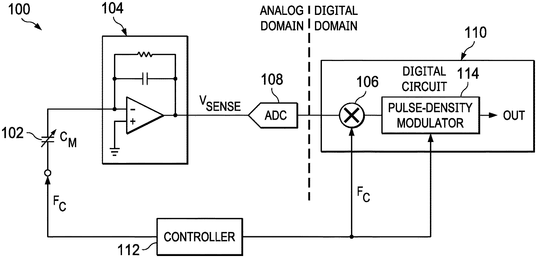
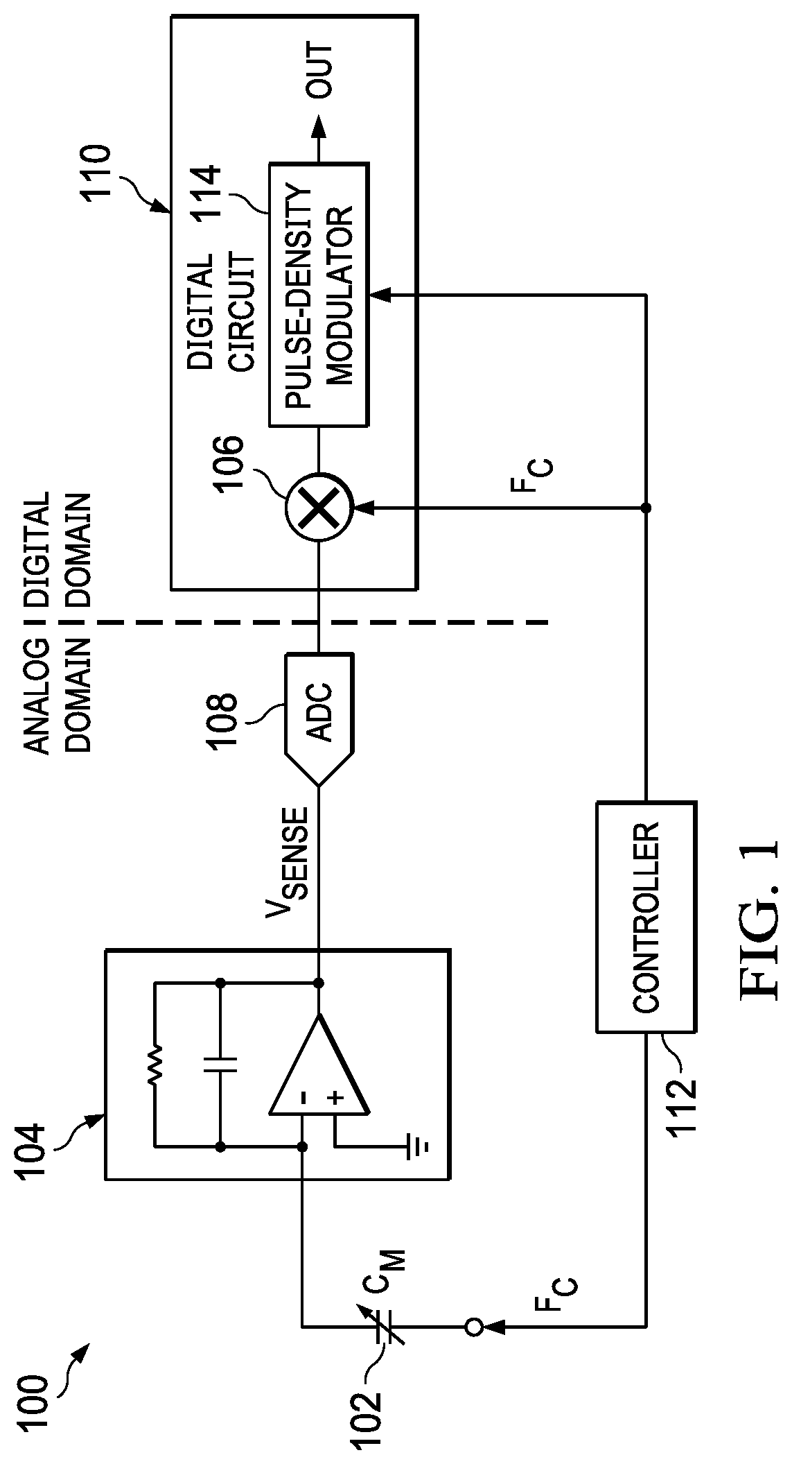
FIG. 1 is a block diagram of selected components of an example capacitance-sensing circuit, in accordance with embodiments of the present disclosure; and
FIG. 2 is a flow chart of an example method for reducing noise in a capacitive sensor having a pulse-density modulator, in accordance with embodiments of the present disclosure.
DETAILED DESCRIPTION
FIG. 1 is a block diagram of selected components of an example capacitance-sensing circuit 100 for sensing a variable capacitance C.sub.M of a component 102, wherein carrier demodulation is implemented in a digital domain, in accordance with embodiments of the present disclosure. In some embodiments, component 102 may comprise an audio speaker and capacitance C.sub.M may be representative of a displacement of an audio transducer of such audio speaker. However, the systems and methods disclosed herein are not limited to measuring displacement in an audio speaker, and may be applied to any suitable measuring or sensing of a capacitance.
As shown in FIG. 1, capacitance sensing circuit 100 may include a capacitance-to-voltage converter (CVC) 104, an analog-to-digital converter (ADC) 108, digital circuitry 110, and a controller 112. CVC 104 may comprise a charge integrator configured to integrate charge at its input to generate a voltage signal V.sub.SENSE indicative of capacitance C.sub.M of component 102. Such voltage signal V.sub.SENSE may be generated by applying an excitation signal at a carrier frequency f.sub.C to one of the terminals of capacitance C.sub.M of component 102, which may cause generation of a modulated voltage signal V.sub.SENSE from a baseband signal indicative of capacitance C.sub.M, wherein the excitation signal is of a carrier frequency f.sub.C which is higher than frequency content of the baseband signal.
ADC 108 may convert modulated voltage signal V.sub.SENSE into an equivalent modulated digital signal that may be further processed by digital circuitry 110. As shown in FIG. 1, ADC 108 may define a boundary between an analog domain of a signal path of capacitance sensing circuit 100 and a digital domain of the signal path of capacitance sensing circuit 100.
As also depicted in FIG. 1, digital circuitry 110 may include a demodulator 106 and a pulse-density modulator 114. Demodulator 106 may demodulate the modulated digital signal from ADC 108 at the carrier frequency f.sub.C in a digital domain of capacitance sensing circuit 100 to generate a digital signal representative of a capacitance of the capacitor wherein the demodulating is based, at least in part, on the excitation signal. For example, the demodulation signal received by demodulator 106 may comprise a sine wave at carrier frequency f.sub.C. Pulse-density modulator 114 may comprise any system, device, or apparatus configured to receive the digital signal output by demodulator 106 and modulate such signal to create an equivalent pulse-density modulated signal OUT, such that pulse-density modulated signal OUT is representative of capacitance C.sub.M of component 102.
Controller 112 may be configured to apply the excitation signal to one of the terminals of capacitance C.sub.M of component 102 as described above. In some embodiments, such excitation signal may comprise a square-wave signal. Controller 112 may also be configured to generate a digital equivalent of the excitation signal (e.g., a sine wave at carrier frequency f.sub.C) to demodulator 106 such that demodulator 106 demodulates the modulated digital signal generated by ADC 108 as described above.
Further, pulse-density modulator 114 may have a noise transfer function, and controller 112 may be configured to control the noise transfer function (e.g., by communicating one or more appropriate control signals) of pulse-density modulator 114 in order to shape the noise transfer function of pulse-density modulator 114 to have an approximate zero at carrier frequency f.sub.C, in order to reduce or eliminate coupling of noise from the output of pulse-density modulator 114 to the capacitor of component 102. In some embodiments, pulse-density modulator 114 may be able to vary the approximate zero of the noise transfer function of pulse-density modulator 114 responsive to changes in carrier frequency f.sub.C. For example, in some embodiments, such changes in carrier frequency f.sub.C may occur in order to reduce noise or interference at a certain frequency from appearing in the modulated signal.
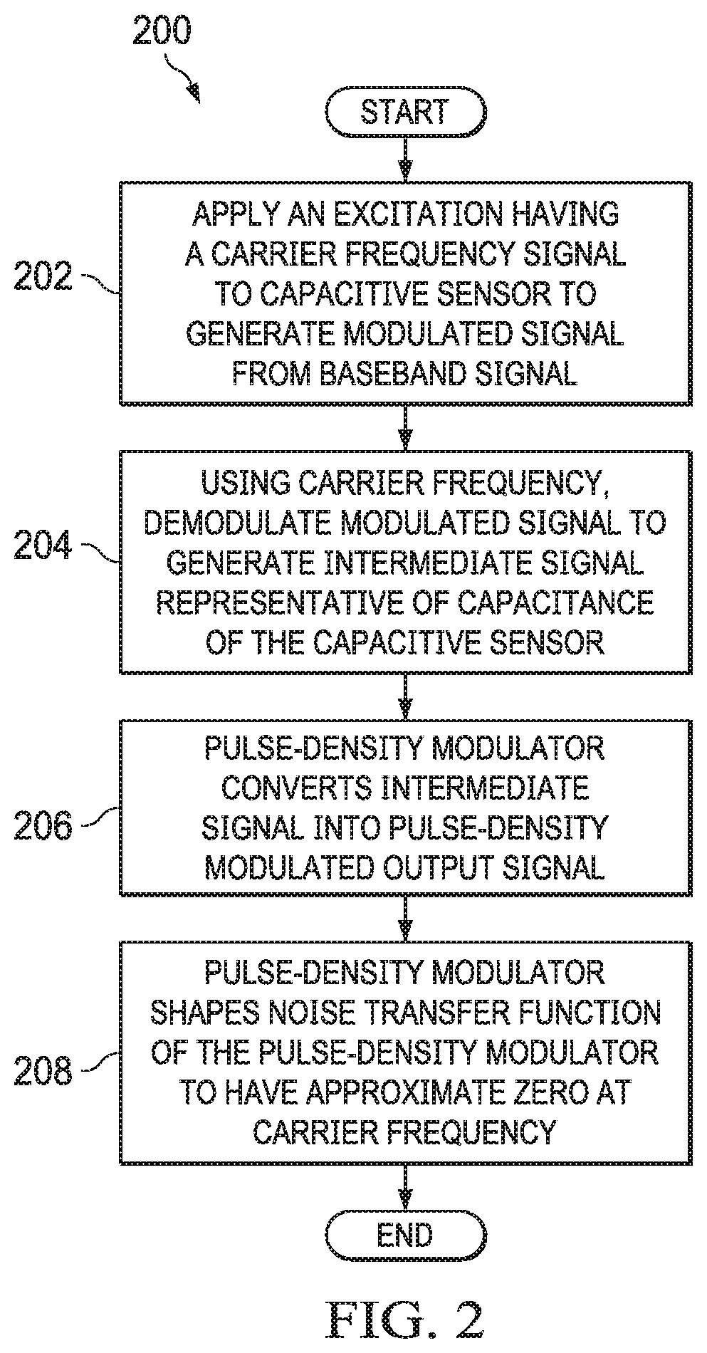
FIG. 2 is a flow chart of an example method 200 for reducing noise in a capacitive sensor having a pulse-density modulator, in accordance with embodiments of the present disclosure. According to certain embodiments, method 200 may begin at step 202. As noted above, teachings of the present disclosure may be implemented in a variety of configurations of a capacitive sensing circuit. As such, the preferred initialization point for method 200 and the order of the steps comprising method 200 may depend on the implementation chosen. In these and other embodiments, method 200 may be implemented as firmware, software, applications, functions, libraries, or other instructions.
At step 202, a signal generator (e.g., controller 112) may apply an excitation signal to a capacitor of a capacitive sensor (e.g., component 102) which causes generation of a modulated signal from a baseband signal, wherein the excitation signal is of a carrier frequency (e.g., carrier frequency f.sub.C) which is higher than frequency content of the baseband signal. At step 204, a demodulator (e.g., demodulator 106) may demodulate the modulated signal to generate an intermediate digital signal representative of a capacitance of the capacitor wherein the demodulating is based, at least in part, on the excitation signal (e.g., at carrier frequency f.sub.C). In some embodiments, the modulated signal may comprise a digital signal and demodulating the modulated signal may comprise demodulating the modulated signal in a digital domain.
At step 206, a pulse-density modulator (e.g., pulse-density modulator 114) may convert the intermediate signal into a pulse-density modulated output signal (e.g., pulse-density modulated output signal OUT). In some embodiments, the pulse-density modulated output signal may be a one-bit signal.
At step 208, the pulse-density modulator, alone or in concert with an appropriate controller (e.g., controller 112), may shape a noise transfer function of the pulse-density modulator to have an approximate zero at the carrier frequency. In some embodiments, the approximate zero may vary in accordance with variances or changes of the carrier frequency.
Although FIG. 2 discloses a particular number of steps to be taken with respect to method 200, method 200 may be executed with greater or fewer steps than those depicted in FIG. 2. In addition, although FIG. 2 discloses a certain order of steps to be taken with respect to method 200, the steps comprising method 200 may be completed in any suitable order.
Method 200 may be implemented in whole or part using sensing circuit 100, components thereof or any other system operable to implement method 200. In certain embodiments, method 200 may be implemented partially or fully in software and/or firmware embodied in computer-readable media.
As used herein, when two or more elements are referred to as "coupled" to one another, such term indicates that such two or more elements are in electronic communication or mechanical communication, as applicable, whether connected indirectly or directly, with or without intervening elements.
This disclosure encompasses all changes, substitutions, variations, alterations, and modifications to the exemplary embodiments herein that a person having ordinary skill in the art would comprehend. Similarly, where appropriate, the appended claims encompass all changes, substitutions, variations, alterations, and modifications to the exemplary embodiments herein that a person having ordinary skill in the art would comprehend. Moreover, reference in the appended claims to an apparatus or system or a component of an apparatus or system being adapted to, arranged to, capable of, configured to, enabled to, operable to, or operative to perform a particular function encompasses that apparatus, system, or component, whether or not it or that particular function is activated, turned on, or unlocked, as long as that apparatus, system, or component is so adapted, arranged, capable, configured, enabled, operable, or operative.
All examples and conditional language recited herein are intended for pedagogical objects to aid the reader in understanding this disclosure and the concepts contributed by the inventor to furthering the art, and are construed as being without limitation to such specifically recited examples and conditions. Although embodiments of the present disclosure have been described in detail, it should be understood that various changes, substitutions, and alterations could be made hereto without departing from the spirit and scope of the disclosure.
* * * * *
D00000
D00001
D00002
XML
uspto.report is an independent third-party trademark research tool that is not affiliated, endorsed, or sponsored by the United States Patent and Trademark Office (USPTO) or any other governmental organization. The information provided by uspto.report is based on publicly available data at the time of writing and is intended for informational purposes only.
While we strive to provide accurate and up-to-date information, we do not guarantee the accuracy, completeness, reliability, or suitability of the information displayed on this site. The use of this site is at your own risk. Any reliance you place on such information is therefore strictly at your own risk.
All official trademark data, including owner information, should be verified by visiting the official USPTO website at www.uspto.gov. This site is not intended to replace professional legal advice and should not be used as a substitute for consulting with a legal professional who is knowledgeable about trademark law.