Structurally controlled deposition of silicon onto nanowires
Wang , et al.
U.S. patent number 10,707,484 [Application Number 15/887,809] was granted by the patent office on 2020-07-07 for structurally controlled deposition of silicon onto nanowires. This patent grant is currently assigned to Amprius, Inc.. The grantee listed for this patent is Amprius, Inc.. Invention is credited to Jonathan Bornstein, Song Han, Zuqin Liu, Constantin Ionel Stefan, Weijie Wang.


View All Diagrams
| United States Patent | 10,707,484 |
| Wang , et al. | July 7, 2020 |
Structurally controlled deposition of silicon onto nanowires
Abstract
Provided herein are nanostructures for lithium ion battery electrodes and methods of fabrication. In some embodiments, a nanostructure template coated with a silicon coating is provided. The silicon coating may include a non-conformal, more porous layer and a conformal, denser layer on the non-conformal, more porous layer. In some embodiments, two different deposition processes, e.g., a PECVD layer to deposit the non-conformal layer and a thermal CVD process to deposit the conformal layer, are used. Anodes including the nanostructures have longer cycle lifetimes than anodes made using either a PECVD or thermal CVD method alone.
| Inventors: | Wang; Weijie (Sunnyvale, CA), Liu; Zuqin (Sunnyvale, CA), Han; Song (Foster City, CA), Bornstein; Jonathan (Cupertino, CA), Stefan; Constantin Ionel (San Jose, CA) | ||||||||||
|---|---|---|---|---|---|---|---|---|---|---|---|
| Applicant: |
|
||||||||||
| Assignee: | Amprius, Inc. (Fremont,
CA) |
||||||||||
| Family ID: | 54368596 | ||||||||||
| Appl. No.: | 15/887,809 | ||||||||||
| Filed: | February 2, 2018 |
Prior Publication Data
| Document Identifier | Publication Date | |
|---|---|---|
| US 20190088939 A1 | Mar 21, 2019 | |
Related U.S. Patent Documents
| Application Number | Filing Date | Patent Number | Issue Date | ||
|---|---|---|---|---|---|
| 14710103 | May 12, 2015 | 9923201 | |||
| 61992121 | May 12, 2014 | ||||
| Current U.S. Class: | 1/1 |
| Current CPC Class: | H01M 4/0428 (20130101); H01M 4/386 (20130101); H01M 4/134 (20130101); H01M 4/366 (20130101); H01M 10/0525 (20130101); H01M 4/1395 (20130101); H01M 10/052 (20130101); H01M 2004/027 (20130101) |
| Current International Class: | H01M 4/04 (20060101); H01M 10/052 (20100101); H01M 4/38 (20060101); H01M 4/36 (20060101); H01M 4/1395 (20100101); H01M 10/0525 (20100101); H01M 4/134 (20100101); H01M 4/02 (20060101) |
References Cited [Referenced By]
U.S. Patent Documents
| 4366215 | December 1982 | Coetzer et al. |
| 4436796 | March 1984 | Huggins et al. |
| 5426006 | June 1995 | Delnick et al. |
| 5457343 | October 1995 | Ajayan |
| 5702845 | December 1997 | Kawakami et al. |
| 5855860 | January 1999 | Nishimine |
| 5997832 | December 1999 | Lieber |
| 6025094 | February 2000 | Visco et al. |
| 6083644 | July 2000 | Watanabe et al. |
| 6090505 | July 2000 | Shimamura et al. |
| 6238821 | May 2001 | Mukherjee et al. |
| 6334939 | January 2002 | Zhou |
| 6355377 | March 2002 | Sheem et al. |
| 6423453 | July 2002 | Noda |
| 6514395 | February 2003 | Zhou |
| 6667099 | December 2003 | Greiner et al. |
| 7189476 | March 2007 | Macklin et al. |
| 7402829 | July 2008 | Green |
| 7408829 | August 2008 | Kuang et al. |
| 7438759 | October 2008 | Zhang et al. |
| 7682750 | March 2010 | Chen |
| 7704480 | April 2010 | Jiang et al. |
| 7794840 | June 2010 | Grigorian et al. |
| 7816031 | October 2010 | Cui et al. |
| 7816709 | October 2010 | Balzano et al. |
| 7951489 | May 2011 | Kim et al. |
| 8017272 | September 2011 | Feng et al. |
| 8202568 | June 2012 | Lin et al. |
| 8206569 | June 2012 | Lopatin et al. |
| 8241372 | August 2012 | Cheng et al. |
| 8252245 | August 2012 | Tonkovich et al. |
| 8257866 | September 2012 | Loveness et al. |
| 8263258 | September 2012 | Nakazato et al. |
| 8367240 | February 2013 | Honda |
| 8420258 | April 2013 | Rojeski |
| 8450012 | May 2013 | Cui et al. |
| 8481214 | July 2013 | Rojeski |
| 8491718 | July 2013 | Chaudhari |
| 8556996 | October 2013 | Loveness et al. |
| 8568914 | October 2013 | Pol et al. |
| 8652683 | February 2014 | Rojeski |
| 8709654 | April 2014 | Takeuchi |
| 8828481 | September 2014 | Burton et al. |
| 8877374 | November 2014 | Cui et al. |
| 8900748 | December 2014 | Cho |
| 9172088 | October 2015 | Loveness et al. |
| 9172094 | October 2015 | Loveness et al. |
| 9231243 | January 2016 | Cui et al. |
| 9698410 | July 2017 | Fasching et al. |
| 9780365 | October 2017 | Liu et al. |
| 9923201 | March 2018 | Wang et al. |
| 10090512 | October 2018 | Cui et al. |
| 10096817 | October 2018 | Loveness et al. |
| 10230101 | March 2019 | Loveness et al. |
| 10461359 | October 2019 | Cui et al. |
| 2002/0028384 | March 2002 | Krasnov et al. |
| 2002/0102461 | August 2002 | Baker et al. |
| 2002/0148727 | October 2002 | Zhou et al. |
| 2003/0175589 | September 2003 | Kaminaka et al. |
| 2003/0178104 | September 2003 | Sekine |
| 2003/0203139 | October 2003 | Ren et al. |
| 2004/0023111 | February 2004 | Ohshita et al. |
| 2004/0126653 | July 2004 | Visco et al. |
| 2004/0126659 | July 2004 | Graetz et al. |
| 2004/0197641 | October 2004 | Visco et al. |
| 2005/0100793 | May 2005 | Jonghe et al. |
| 2005/0153208 | July 2005 | Konishiike et al. |
| 2005/0175901 | August 2005 | Kawakami et al. |
| 2005/0238810 | October 2005 | Scaringe et al. |
| 2005/0279274 | December 2005 | Nui et al. |
| 2006/0040182 | February 2006 | Kawakami et al. |
| 2006/0066201 | March 2006 | Ra et al. |
| 2006/0097691 | May 2006 | Green |
| 2006/0147797 | July 2006 | Wu et al. |
| 2006/0154141 | July 2006 | Salot et al. |
| 2006/0165988 | July 2006 | Chiang et al. |
| 2006/0204853 | September 2006 | Chen |
| 2006/0216603 | September 2006 | Choi |
| 2006/0258133 | November 2006 | Georgiev et al. |
| 2006/0261134 | November 2006 | Ho |
| 2007/0065720 | March 2007 | Hasegawa et al. |
| 2007/0095276 | May 2007 | Sunkara et al. |
| 2007/0117007 | May 2007 | Visco et al. |
| 2007/0148544 | June 2007 | Le |
| 2007/0154808 | July 2007 | Konishiike et al. |
| 2007/0190422 | August 2007 | Morris |
| 2007/0212538 | September 2007 | Niu |
| 2007/0298168 | December 2007 | Ajayan et al. |
| 2008/0008844 | January 2008 | Bettge et al. |
| 2008/0038638 | February 2008 | Zhang et al. |
| 2008/0044732 | February 2008 | Salot et al. |
| 2008/0057399 | March 2008 | Visco et al. |
| 2008/0087314 | April 2008 | Xiao et al. |
| 2008/0110486 | May 2008 | Tsakalokos et al. |
| 2008/0145762 | June 2008 | Adachi et al. |
| 2008/0161746 | July 2008 | Visco et al. |
| 2008/0213603 | July 2008 | Kobayashi et al. |
| 2008/0206641 | August 2008 | Christensen et al. |
| 2008/0261116 | October 2008 | Burton et al. |
| 2008/0274403 | November 2008 | Kim et al. |
| 2008/0280169 | November 2008 | Niu et al. |
| 2008/0280207 | November 2008 | Patoux et al. |
| 2009/0004566 | January 2009 | Shirane et al. |
| 2009/0029256 | January 2009 | Mah |
| 2009/0042102 | February 2009 | Cui et al. |
| 2009/0061319 | March 2009 | Kim et al. |
| 2009/0068553 | March 2009 | Firsich et al. |
| 2009/0117472 | May 2009 | Iwamoto |
| 2009/0162746 | June 2009 | Honda |
| 2009/0169996 | July 2009 | Zhamu et al. |
| 2009/0176159 | July 2009 | Zhamu et al. |
| 2009/0186267 | July 2009 | Tiegs |
| 2009/0188544 | July 2009 | Kobayashi et al. |
| 2009/0202908 | August 2009 | Sumihara et al. |
| 2009/0202915 | August 2009 | Modeki et al. |
| 2009/0214942 | August 2009 | Frank et al. |
| 2009/0214944 | August 2009 | Rojeski |
| 2009/0246628 | October 2009 | Adachi et al. |
| 2009/0269511 | October 2009 | Zhamu et al. |
| 2009/0291371 | November 2009 | Konishiike et al. |
| 2009/0305131 | December 2009 | Kumar et al. |
| 2009/0305135 | December 2009 | Shi et al. |
| 2009/0311605 | December 2009 | Visco et al. |
| 2009/0316335 | December 2009 | Simon et al. |
| 2010/0043877 | February 2010 | Wang et al. |
| 2010/0119948 | May 2010 | Hasegawa et al. |
| 2010/0122725 | May 2010 | Buchine et al. |
| 2010/0159337 | June 2010 | Matsumoto et al. |
| 2010/0176337 | July 2010 | Zhamu et al. |
| 2010/0209775 | August 2010 | Kim et al. |
| 2010/0237272 | September 2010 | Chaudhari |
| 2010/0266897 | October 2010 | Lee et al. |
| 2010/0285358 | November 2010 | Cui et al. |
| 2010/0291441 | November 2010 | Ugaji et al. |
| 2010/0297502 | November 2010 | Zhu et al. |
| 2010/0310941 | December 2010 | Kumta et al. |
| 2010/0330421 | December 2010 | Cui et al. |
| 2010/0330423 | December 2010 | Cui et al. |
| 2011/0008233 | January 2011 | Miyanaga |
| 2011/0027655 | February 2011 | Rojeski |
| 2011/0111294 | May 2011 | Lopez et al. |
| 2011/0111300 | May 2011 | DelHagen et al. |
| 2011/0111304 | May 2011 | Cui et al. |
| 2011/0135925 | June 2011 | Zhamu et al. |
| 2011/0143019 | June 2011 | Mosso et al. |
| 2011/0143263 | June 2011 | Shirvanian et al. |
| 2011/0159365 | June 2011 | Loveness et al. |
| 2011/0159367 | June 2011 | Kim et al. |
| 2011/0189510 | August 2011 | Caracciolo et al. |
| 2011/0205688 | August 2011 | Ray et al. |
| 2011/0229761 | September 2011 | Cui et al. |
| 2011/0269025 | November 2011 | Sun et al. |
| 2011/0287318 | November 2011 | Loveness et al. |
| 2012/0028123 | February 2012 | Asari et al. |
| 2012/0034524 | February 2012 | Caracciolo et al. |
| 2012/0070741 | March 2012 | Liu et al. |
| 2012/0094192 | April 2012 | Jun et al. |
| 2012/0183856 | July 2012 | Cui et al. |
| 2012/0292586 | November 2012 | Yamauchi et al. |
| 2012/0301785 | November 2012 | Buchine et al. |
| 2012/0301789 | November 2012 | Loveness et al. |
| 2012/0328942 | December 2012 | Thomas-Alyea et al. |
| 2013/0004657 | January 2013 | Xu et al. |
| 2013/0011736 | January 2013 | Loveness et al. |
| 2013/0069601 | March 2013 | Coowar et al. |
| 2013/0078523 | March 2013 | Rojeski |
| 2013/0143124 | June 2013 | Lee et al. |
| 2013/0320582 | December 2013 | Cui et al. |
| 2013/0344383 | December 2013 | Loveness et al. |
| 2015/0325852 | November 2015 | Wang et al. |
| 2016/0013483 | January 2016 | Loveness et al. |
| 2016/0190600 | June 2016 | Cui et al. |
| 2017/0098819 | April 2017 | Loveness et al. |
| 2017/0338464 | November 2017 | Fasching et al. |
| 2018/0090755 | March 2018 | Liu et al. |
| 2019/0273252 | January 2019 | Loveness et al. |
| 2019/0058186 | February 2019 | Cui et al. |
| 1891668 | Jan 2004 | CN | |||
| 1476645 | Feb 2004 | CN | |||
| 1705418 | Dec 2005 | CN | |||
| 1979828 | Jun 2007 | CN | |||
| 101346834 | Jan 2009 | CN | |||
| 101346836 | Jan 2009 | CN | |||
| 101356666 | Jan 2009 | CN | |||
| 101356670 | Jan 2009 | CN | |||
| 101453013 | Jun 2009 | CN | |||
| 101527357 | Sep 2009 | CN | |||
| 101560694 | Oct 2009 | CN | |||
| 101689628 | Mar 2010 | CN | |||
| 101453016 | Jun 2010 | CN | |||
| 101356666 | Oct 2010 | CN | |||
| 101953014 | Jan 2011 | CN | |||
| 101986447 | Mar 2011 | CN | |||
| 101989655 | Mar 2011 | CN | |||
| 102460782 | May 2012 | CN | |||
| 101689628 | Jun 2012 | CN | |||
| 102959775 | Mar 2013 | CN | |||
| 883199 | Dec 1998 | EP | |||
| 1 205 989 | May 2002 | EP | |||
| 845828 | Oct 2002 | EP | |||
| 1494302 | Jan 2005 | EP | |||
| 1 873 846 | Jan 2008 | EP | |||
| 2 219 250 | Aug 2010 | EP | |||
| 2427928 | Mar 2012 | EP | |||
| 2880198 | Jun 2006 | FR | |||
| 2470056 | Nov 2010 | GB | |||
| 2000-036323 | Feb 2000 | JP | |||
| 2002-216751 | Aug 2002 | JP | |||
| 2003-303588 | Oct 2003 | JP | |||
| 2005-259697 | Sep 2005 | JP | |||
| 2005-310759 | Nov 2005 | JP | |||
| 2006-269306 | Oct 2006 | JP | |||
| 2007-061945 | Mar 2007 | JP | |||
| 2007/123100 | May 2007 | JP | |||
| 2008-026595 | Feb 2008 | JP | |||
| 2008-192594 | Aug 2008 | JP | |||
| 2008/235258 | Oct 2008 | JP | |||
| 2008-269827 | Nov 2008 | JP | |||
| 2008-305781 | Dec 2008 | JP | |||
| 2009-021226 | Jan 2009 | JP | |||
| 2009-032693 | Feb 2009 | JP | |||
| 2009117165 | May 2009 | JP | |||
| 2009-164137 | Jul 2009 | JP | |||
| 2010-525549 | Jul 2010 | JP | |||
| 2010-262752 | Nov 2010 | JP | |||
| 2010/538444 | Dec 2010 | JP | |||
| 2011108639 | Jun 2011 | JP | |||
| 2012-526364 | Oct 2012 | JP | |||
| 2012-527735 | Nov 2012 | JP | |||
| 2013-65547 | Apr 2013 | JP | |||
| 2013-521621 | Jun 2013 | JP | |||
| 2012556203 | Jun 2013 | JP | |||
| 2005-071655 | Mar 2016 | JP | |||
| 6250538 | Dec 2017 | JP | |||
| 2006-0047424 | May 2006 | KR | |||
| 2007-0043950 | Apr 2007 | KR | |||
| 2008-0070769 | Jul 2008 | KR | |||
| 2009/0019339 | Feb 2009 | KR | |||
| 2010 0113433 | Oct 2010 | KR | |||
| 2006/123049 | Nov 2006 | WO | |||
| 2007/083152 | Jan 2007 | WO | |||
| 2007/061945 | May 2007 | WO | |||
| 2007/071778 | Jun 2007 | WO | |||
| 2007/083155 | Feb 2008 | WO | |||
| 2008/044449 | Apr 2008 | WO | |||
| 2008/139157 | Nov 2008 | WO | |||
| 2009/008558 | Jan 2009 | WO | |||
| 2009/009206 | Jan 2009 | WO | |||
| 2009/010757 | Jan 2009 | WO | |||
| 2009/010758 | Jan 2009 | WO | |||
| 2009/010759 | Jan 2009 | WO | |||
| 2009/031715 | Mar 2009 | WO | |||
| 2009/033015 | Mar 2009 | WO | |||
| 2009/129490 | Oct 2009 | WO | |||
| 2010/100599 | Sep 2010 | WO | |||
| 2010/129910 | Nov 2010 | WO | |||
| 2010/138617 | Dec 2010 | WO | |||
| 2010/138619 | Dec 2010 | WO | |||
| 2011/015174 | Feb 2011 | WO | |||
| 2011/053553 | May 2011 | WO | |||
| 2011/053736 | May 2011 | WO | |||
| 2011/056847 | May 2011 | WO | |||
| 2011/066818 | Jun 2011 | WO | |||
| 2011/094642 | Aug 2011 | WO | |||
| 2011/109477 | Sep 2011 | WO | |||
| 2011/137446 | Nov 2011 | WO | |||
| 2011/149958 | Dec 2011 | WO | |||
| 2012/027360 | Mar 2012 | WO | |||
| 2012/054767 | Apr 2012 | WO | |||
| 2013-096931 | Jun 2013 | WO | |||
| 2014/008433 | Jan 2014 | WO | |||
| 2015/175509 | Nov 2015 | WO | |||
Other References
|
Machine translation of JP 2006-269306, published on Oct. 5, 2006 (Year: 2006). cited by examiner . U.S. Appl. No. 12/437,529, Office Action dated May 13, 2011. cited by applicant . U.S. Appl. No. 12/437,529, Office Action dated Oct. 20, 2011. cited by applicant . U.S. Appl. No. 12/437,529, Office Action dated Dec. 22, 2011. cited by applicant . U.S. Office Action dated Oct. 25, 2012 issued in U.S. Appl. No. 13/427,681. cited by applicant . U.S. Appl. No. 13/427,681, Final Office Action dated Jun. 11, 2013. cited by applicant . U.S. Appl. No. 13/427,681, Office Action dated Oct. 2, 2013. cited by applicant . U.S. Appl. No. 13/427,681, Office Action dated May 21, 2014. cited by applicant . U.S. Appl. No. 13/427,681, Office Action dated Feb. 6, 2015. cited by applicant . Examiner's Answer, dated Sep. 28, 2016, issued in U.S. Appl. No. 13/427,681. cited by applicant . Board of Appeal Decision, dated Nov. 15, 2017, issued in U.S. Appl. No. 13/427,681. cited by applicant . CN patent application No. 201080026302.6, Office Action dated Oct. 23, 2013. cited by applicant . CN patent application No. 201080026302.6, Office Action dated Aug. 8, 2014. cited by applicant . CN patent application No. 201080026302.6, Office Action dated Mar. 23, 2015. cited by applicant . CN patent application No. 201080026302.6, Office Action dated Nov. 10, 2015. cited by applicant . EP patent application No. 10772907.1, Supplemental European Search Report dated Jul. 4, 2013. cited by applicant . JP patent application No. 2012-510025, Notice of Reasons for Rejection dated Jan. 7, 2014. cited by applicant . JP patent application No. 2012-510025, Decision of Rejection dated Aug. 5, 2014. cited by applicant . IL patent application No. 216100, Office Action dated May 4, 2015. cited by applicant . IL patent application No. 216100, Office Action (Notification of Deficiencies Prior to Allowance of Patent Application) dated Jun. 22, 2016. cited by applicant . WO patent application No. PCT/US2010/034106, International Search Report and Written Opinion dated Feb. 7, 2011. cited by applicant . U.S. Appl. No. 12/787,168, Office Action dated Jan. 10, 2013. cited by applicant . U.S. Appl. No. 12/787,168, Office Action dated Sep. 10, 2013. cited by applicant . U.S. Appl. No. 12/787,168, Office Action dated Feb. 26, 2014. cited by applicant . U.S. Appl. No. 12/787,168, Final Office Action dated Nov. 6, 2014. cited by applicant . U.S. Appl. No. 12/787,168, Non-Final Office Action dated Jul. 7, 2015. cited by applicant . U.S. Appl. No. 12/787,168, Final Office Action dated Apr. 11, 2016. cited by applicant . U.S. Appl. No. 12/787,168, Office Action dated Mar. 9, 2017. cited by applicant . U.S. Appl. No. 12/787,168, Final Office Action dated Dec. 20, 2017. cited by applicant . CN patent application No. 201080023345.9, Office Action dated Dec. 27, 2013. cited by applicant . CN patent application No. 201080023345.9, Office Action dated Sep. 11, 2014. cited by applicant . CN patent application No. 201080023345.9, Office Action dated Apr. 16, 2015. cited by applicant . EP patent application No. 10781151.5, Supplemental European Search Report dated Jun. 28, 2013. cited by applicant . JP patent application No. 2012-513225, Notification of Reasons for Rejection dated Dec. 17, 2013. cited by applicant . JP patent application No. 2012-513225, Decision for Grant and Allowed Claims received Jul. 17, 2014. cited by applicant . Korean Notification of Provisional Rejection dated Aug. 19, 2015, KR patent application No. 10-2011-7031120. cited by applicant . Korean Notice of First Refusal Ruling dated Apr. 28, 2016, KR patent application No. 10-2011-7031120. cited by applicant . Israel Office Action dated Oct. 13, 2015, IL patent application No. 216248. cited by applicant . WO patent application No. PCT/US2010/036235, International Search Report and Written Opinion dated Jan. 28, 2001. cited by applicant . Office Action dated Apr. 5, 2012 for U.S. Appl. No. 13/039,031. cited by applicant . Notice of allowance dated Jul. 26, 2012 for U.S. Appl. No. 13/039,031. cited by applicant . U.S. Office Action dated Sep. 17, 2012 issued in U.S. Appl. No. 13/540,484. cited by applicant . U.S. Appl. No. 13/540,484, Notice of Allowance dated Feb. 22, 2013. cited by applicant . Pre-Issuance Submission by Third Party dated Jan. 15, 2014, received in U.S. Appl. No. 13/914,491. cited by applicant . U.S. Appl. No. 13/914,491, Office Action dated Dec. 3, 2014. cited by applicant . U.S. Appl. No. 13/914,491, Notice of Allowance dated Jun. 19, 2015. cited by applicant . Office Action dated Jan. 2, 2018 for U.S. Appl. No. 14/859,125. cited by applicant . CN patent application No. 201180019460.3, Office Action dated Jul. 2, 2014. cited by applicant . CN patent application No. 201180019460.3, Office Action dated May 6, 2015. cited by applicant . CN patent application No. 201510674597.2, Office Action and Search Report dated Mar. 28, 2017. cited by applicant . CN patent application No. 11751259.0, Office Action dated Dec. 12, 2016. cited by applicant . CN patent application No. 11751259.0, Extended Search Report dated Mar. 16, 2017. cited by applicant . JP patent application No. 2012-556203, Office Action dated Aug. 26, 2014. cited by applicant . JP patent application No. 2012-556203, Office Action dated Jul. 14, 2015. cited by applicant . JP patent application No. 2016-077671, Office Action dated Jul. 4, 2017. cited by applicant . KR patent application No. 10-2012-7024928, Office Action dated Aug. 28, 2017. cited by applicant . TW patent publication No. 201238125, published Sep. 16, 2012, English Abstract. cited by applicant . TW patent application No. 100120247, Office Action dated Feb. 9, 2015. cited by applicant . WO patent application No. PCT/US2011/026816, International Search Report and Written Opinion dated Oct. 18, 2011. cited by applicant . Office Action dated Apr. 26, 2012, issued in U.S. Appl. No. 12/787,138. cited by applicant . Final Office Action dated Oct. 11, 2012, issued in U.S. Appl. No. 12/787,138. cited by applicant . U.S. Appl. No. 12/787,138, Notice of Allowance dated Jan. 28, 2013. cited by applicant . U.S. Appl. No. 13/891,035, Office Action dated Jun. 19, 2014. cited by applicant . U.S. Appl. No. 13/891,035, Final Office Action dated Apr. 23, 2015. cited by applicant . U.S. Appl. No. 13/891,035, Notice of Allowance dated Aug. 26, 2015. cited by applicant . U.S. Appl. No. 13/891,035, Supplemental Notice of Allowance dated Sep. 23, 2015. cited by applicant . U.S. Appl. No. 14/952,744, filed Nov. 25, 2015. cited by applicant . U.S. Appl. No. 14/952,744, filed Sep. 27, 2016. cited by applicant . U.S. Appl. No. 14/952,744, Final Office Action dated Aug. 25, 2017. cited by applicant . CN patent application No. 201080023257.9, Chinese Office Action dated Dec. 12, 2013. cited by applicant . CN patent application No. 201080023257.9, Chinese Office Action dated Oct. 21, 2014. cited by applicant . CN patent application No. 201080023257.9, Chinese Office Action dated Jun. 4, 2015. cited by applicant . Israel Office Action dated Aug. 10, 2015, IL patent application No. 216246. cited by applicant . IL patent application No. 216100, Office Action dated Jan. 20, 2016. cited by applicant . IL patent application No. 216100, Office Action dated Jun. 29, 2017. cited by applicant . JP patent application No. 2012-513226, Japanese Office Action dated Feb. 4, 2014. cited by applicant . JP patent application No. 2012-513226, Japanese Office Action dated Feb. 10, 2015. cited by applicant . Japanese Office Action dated Aug. 25, 2015, JP patent application No. 2012-513226. cited by applicant . WO patent application No. PCT/US2010/036237, International Search Report dated Feb. 1, 2011. cited by applicant . WO patent application No. PCT/US2010/036237, Written Opinion dated Feb. 1, 2011. cited by applicant . U.S. Appl. No. 13/114,413, Office Action dated Jun. 19, 2014. cited by applicant . U.S. Appl. No. 13/114,413, Notice to Allowance dated Jan. 22, 2015. cited by applicant . U.S. Appl. No. 13/114,413, Notice of Allowance dated Jun. 24, 2015. cited by applicant . WO patent application No. PCT/US2011/037767, International Search Report and Written Opinion dated Jan. 16, 2012. cited by applicant . U.S. Appl. No. 13/277,821, Office Action dated Feb. 25, 2013. cited by applicant . U.S. Appl. No. 13/277,821, Office Action dated Oct. 11, 2013. cited by applicant . U.S. Appl. No. 13/277,821, Office Action dated Apr. 10, 2014. cited by applicant . U.S. Appl. No. 13/277,821, Final Office Action dated Nov. 20, 2014. cited by applicant . U.S. Appl. No. 13/277,821, Decision on Appeal dated Oct. 18, 2016. cited by applicant . U.S. Appl. No. 13/277,821, Notice of Allowance dated Jan. 4, 2017. cited by applicant . U.S. Appl. No. 13/277,821, Notice of Allowance dated Jun. 1, 2017. cited by applicant . TW Office Action issue in Application No. 100138369, dated Dec. 22, 2015. cited by applicant . TW Office Action issue in Application No. 105142724, dated Nov. 13, 2017. cited by applicant . WO patent application No. PCT/US2011/057159, International Search Report and Written Opinion dated Jun. 11, 2012. cited by applicant . Office Action dated Dec. 7, 2012 in U.S. Appl. No. 13/277,620. cited by applicant . Office Action dated Aug. 29, 2013 in U.S. Appl. No. 13/277,620. cited by applicant . Final Office Action dated Mar. 28, 2014 in U.S. Appl. No. 13/277,620. cited by applicant . Office Action dated Nov. 4, 2014 in U.S. Appl. No. 13/277,620. cited by applicant . Notice of Allowance dated Jul. 31, 2015 in U.S. Appl. No. 13/277,620. cited by applicant . Office Action dated Dec. 31, 2015 in U.S. Appl. No. 14/928,576. cited by applicant . Office Action dated Jun. 21, 2016 in U.S. Appl. No. 14/928,576. cited by applicant . Notice of Allowance dated Oct. 6, 2016 in U.S. Appl. No. 14/928,576. cited by applicant . CN Office Action issued in Application No. 201180057806.9, dated Mar. 30, 2015. cited by applicant . CN Second Office Action issued in Application No. 201180057806.9, dated Nov. 19, 2015. cited by applicant . EP Extended Search Report dated Nov. 19, 2015, issued in Application No. 11835170.9. cited by applicant . JP Notice of Reasons for Rejection dated Sep. 8, 2015, in Application No. 2013-535103. cited by applicant . JP Notice of Reasons for Rejection dated Sep. 6, 2016, in Application No. 2013-535103. cited by applicant . KR Notice of Reasons for Rejection dated Oct. 21, 2017 in Application No. 10-2013-7012809. cited by applicant . KR Notice of Reasons for Rejection dated Feb. 27, 2017 in Application No. 10-2013-7012809. cited by applicant . TW Office Action dated Nov. 13, 2015, in Application No. 100138361. cited by applicant . International Search Report and Written Opinion dated Jun. 28, 2012, issued in Application No. PCT/US2011/057158. cited by applicant . U.S. Appl. No. 13/540,484, "Template Electrode Structures with Enhanced Adhesion Characteristics," Liu et al., filed Jul. 2, 2012. cited by applicant . Pre-Issuance Submission by Third Party dated Jan. 21, 2014, received in U.S. Appl. No. 13/540,484. cited by applicant . U.S. Appl. No. 13/914,491, Office Action dated Jan. 8, 2016. cited by applicant . CN Office Action issued in Application No. 201280038037.2 dated Aug. 5, 2015. cited by applicant . CN Office Action issued in application No. 201280038037.2, dated May 26, 2016. cited by applicant . CN Office Action issued in Application No. 201280038037.2 dated Feb. 6, 2017. cited by applicant . EP Search Report issued in Application No. 12807729.4 dated Feb. 5, 2015. cited by applicant . EP Search Report issued in Application No. 12807729.4 dated Jun. 2, 2015. cited by applicant . EP Search Report issued in Application No. 12807729.4 dated Jan. 11, 2017. cited by applicant . JP Office Action issued in application No. 2014-519238, dated May 31, 2016. cited by applicant . JP Office Action issued in Application No. 2014-519238 dated Feb. 7, 2017. cited by applicant . WO patent application No. PCT/US2012/045313, International Search Report and Written Opinion dated Jan. 21, 2013. cited by applicant . U.S. Appl. No. 14/710,103, Office Action dated May 22, 2017. cited by applicant . U.S. Appl. No. 14/710,103, Notice of Allowance dated Oct. 27, 2017. cited by applicant . European Extended Search Report dated Dec. 22, 2017, issued in Application No. 15791953.1. cited by applicant . International Search report and Written Opinion dated Aug. 10, 2015, issued in Application No. PCT/US15/30336. cited by applicant . U.S. Appl. No. 11/837,291, Office Action dated Feb. 18, 2009. cited by applicant . U.S. Appl. No. 11/837,291, Office Action dated Oct. 26, 2009. cited by applicant . U.S. Appl. No. 11/837,291, Office Action dated Jan. 7, 2010. cited by applicant . U.S. Appl. No. 11/837,291, Office Action dated Apr. 22, 2010. cited by applicant . U.S. Appl. No. 11/837,291, Notice of Allowance dated Aug. 10, 2010. cited by applicant . U.S. Appl. No. 12/895,424, Office Action dated Nov. 17, 2010. cited by applicant . EP patent application No. 08831531.2, European Search Report dated Oct. 27, 2010. cited by applicant . Aifantis et al., "High energy density lithium batteries", 2010 Wiley-VCH Verlag GmbH & Co. KGaA, Weinheim (Chapter 6: Next--generation anodes for secondary Li--Ion batteries) ISBN: 978-3-527-32407-1. cited by applicant . Baldwin, Richard K., et al. "Solution reduction synthesis of surface stabilized silicon nanoparticles," The Royal Society of Chemistry 2002, Chem. Commun., 2002, 1822-1823. cited by applicant . Campbell et al., "Prepartion of mesoporous silica templated metal nanowire films on foamed nickel substrates," Microporous and Mesoporous Materials 97, 2006, 114-121. cited by applicant . Carbon nanofiber product sheet, Applied Science 2008, downloaded from http://www.apsci.com/ngm-pyrol.html on May 2011. cited by applicant . Chan, C.K., et al., "High Capacity Li Ion Battery Anodes Using Ge Nanowires", Nano Letters, 2008, vol. 8, No. 1, 307-309. cited by applicant . Chan, C.K., et al., High-Performance Lithium Battery Anodes Using Silicon Nanowires, Nature, vol. 3, Jan. 2008. cited by applicant . Chan, Candace K. et al., "Structural and electrochemical study of the reaction of lithium with silicon nanowires," Journal of Power Sources 189 (2009) 34-39. cited by applicant . Chan, Candace K. et al., "Surface chemistry and morphology of the solid electrolyte interphase on silicon nanowire lithium-ion battery anodes," Journal of Power Sources 189 (2009) 1132-1140. cited by applicant . Che, G., et al., "Carbon Nanotubule Membranes for Electrochemical Energy Storage and Production". Nature 393, 346-349 (1998). cited by applicant . Chaudhari, P. et al. "Heteroepitaxial silicon film growth at 600 degree C for an Al-Si eutectic melt," Thin Solid Films 518 (2010) 5368-5371. cited by applicant . Cheng Mu et al., "Silicon nanotube array/gold electrode for direct electrochemistry of cytochrome e," J. Phys. Chem. B 2007, 111, 1491-1495, Nov. 21, 2006. cited by applicant . Cui, Li-Feng et al., "Carbon-silicon core-shell nanowires as high capacity electrode for lithium ion batteries," Nano Letters, published on Aug. 5, 2009 on http://pubs.acs.org. cited by applicant . Cui, Li-Feng et al., "Crystallline-amorphous core-shell silicon nanowires for high capaXcity and high current battery electrodes," Nano Letters, 2009, vol. 9, No. 1 491-495, Dec. 23, 2008. cited by applicant . Cui, Yi et al., "Doping and electrical transport in silicon nanowires", The Journal of Physical Chemistry, vol. 104, No. 22, Jun. 8, 2000. cited by applicant . Dick, et al A New Understanding of Au-Assisted Growth of Ill-V Semiconductor Nanowires, Adv. Funct. Mater. 15, 1603-1610 (2005). cited by applicant . Emmenegger, et al., "Carbon Nanotubes Synthesized on Metallic Substrates," Applied Surface Science, Aug. 1, 2000, pp. 452-456. cited by applicant . Esmanski, Alexei et al., "Silicon inverse-opal-based macroporous materials as negative electrodes for lithium ion batteries," Advanced Functional Materials, 2009, 1999-2010, May 7, 2009. cited by applicant . For high-performance anode material in lithium-ion batteries, After Gutenberg, downloaded from http://jcwinnie.biz/wordpress/?p=2864 on Dec. 25, 2009. cited by applicant . Frackowiak, E., et al., "Electrochemical Storage of Lithium Multiwalled Carbon Nanotubes," Carbon 37, 1999, pp. 61-69. cited by applicant . Gao, et al., "Alloy formation in nanostructured silicon." Adv. Mater. 13, 816-819 (2001). cited by applicant . Givargizov, "Fundamental aspects of VLS growth," Journal of Crystal Growth 31, 20-30 (1975). cited by applicant . Goldstein et al., "Melting in semiconductor nanocrystals," Science 256, 1425-1427 (Jun. 1992). cited by applicant . Green, M., et al Structured silicon anodes for lithium battery applications. Electrochem. Solid State Lett. 6, A75-A79 (2003). cited by applicant . Hertzberg et al., Abstract "SiC nanotubes Cu foil," J. Am. Chem. Soc., 2010, 8548-8549. cited by applicant . Hertzberg et al., "Deformations in Si-Li anodes upon electrochemical alloying in nano-confined space," J. Am. Chem. Soc. 2010, 132, 8548-8549, Apr. 15, 2010. cited by applicant . Hu L., et al. "Si nanoparticle-decorated Si nanowire networks for Li-ion battery anodes," The Royal Society of Chemistry, Chem. Commun., 2011, 47, pp. 367-369. cited by applicant . Huang et al., Catalytic Growth of Zinc Oxide Nanowires by Vapor Transport, Adv. Mater., 13, 113-116 (2001). cited by applicant . Huang et al., Fabrication of Silicon Nanowire Arrays with Controlled Diameter, Length, and Density, Adv. Mater., (2007), 19, 744-748. cited by applicant . Huggins, R.A. & Nix, W.D. Decrepitation Model for Capacity Loss During Cycling of Alloys in Rechargeable Electrochemical Systems, Ionics 6, 57-63 (2000). cited by applicant . Jie Xiao, et al., "Stabilization of silicon anode for Li-ion batteries," Journal of the Electrochemical Society, 157 (10) A1047-A1051, Aug. 2, 2010. cited by applicant . Kang, Kubum et al., "The role of NiOx overlayers on spontaneous growth of NiSix nanowires from Ni seed layers," Nano Letters 2008, vol. 8, No. 2 431-436, Jan. 12, 2008. cited by applicant . Kang, Kibum et al., Unconventional roles of metal catalysts in chemical-vapor syntheses of singel-crystalline nanowires,: Journal of Applied Physics 105, 122407 (2009). cited by applicant . Kasavajjula et al., "Nano- and bulk-silicon-based insertion anodes for lithium-ion secondary cells", Journal of Power Sources 163 (2007) 1003-1039. cited by applicant . Kim, Cheol-Joo et al., "Spontaneous chemical vapor growth of NiSi nanowires and their metallic properties," Advanced Materials, 2007, 19, 3637-3642, Oct. 16, 2007. cited by applicant . Kim Hyesun, et al., "Superior Lithium Electroaactive Mesoporous Si@Carbon Core-Shell Nanowires for Lithium Battery Anode Material," American Chemical Society, Nano Letters, 2008, vol. 8, No. 11, pp. 3688-3691. cited by applicant . Kim, Hyunjung et al., "Three-dimensional porous silicon particles for use in high-performance lithium secondary batteries," Angewandte Chemie, Int. Ed. 2008, 47, 10151-10154, Nov. 17, 2008. cited by applicant . Lee et al., "Anomalous growth and characterization of carbon-coated nickel silicide nanowires," Chemical Physics Letters 384, 2004, pp. 215-218. cited by applicant . Lee, Y.M., et al. SEI layer formation on amorphous Si thin electrode during precycling. J. Electrochem. Soc. 154, A515-A519 (2007). cited by applicant . Levitt, "Whisker Technology." Wiley Interscience, 1970. cited by applicant . Li et al., "A high capacity nano-Si composite anode material for lithium rechargeable batteries," Electrochemical and Solid-State Letters, 2 (11) 547-549 (1999). cited by applicant . Li et al., "Rate capabilities of nanostructured LiMn2O4 electrodes in aqueous electrolyte." J. Electrochem. Soc. 147, 2044-2049 (2000). cited by applicant . Li et al., "Freestanding mesoporous quasi-single-crystalline Co3O4 nanowire arrays," J. Am. Chem. Soc. 2006, 128, 14258-14259, Oct. 18, 2006. cited by applicant . Magasinski et al., "Hierarchical botton-up approach for high-performance Si-based Li-ion battery anodes," Abstract #16, IMLB 2010, The Electrochemical Society. cited by applicant . Magasinki, A. et al., "High-performance lithium-ion anodes using a hierarchical bottom-up approach," Nature Materials, published online at www.nature.com/naturematerials Mar. 14, 2010. cited by applicant . Magasinski et al., "Towards efficent binders for Li-ion battery Si-based anodes," Abstract #64, IMLB 2010, The Electrochemical Society. cited by applicant . Marczak et al., "The individual core/shell silicon nanowire structure probed by Raman spetroscopy," Raman Spetroscopy, Phys. Status Solidi C 6 No. 9, 2053-2055, 2009. cited by applicant . Morales, et al., A Laser Ablation Method for the Synthesis of Crystalline Semiconductor Nanowires, Science vol. 279, Jan. 9, 1998. cited by applicant . Nickel Silicide Nanobelts and Sheets in Li-ion Anodes Capacity, Green Car Congress, Apr. 19, 2009, pp. 1-3. cited by applicant . Nishi, Yoshio, "Lithium ion secondary batteries; past 10 years and the future," Journal of Power Sources, vol. 100, 2001, pp. 101-106. cited by applicant . Pan et al., Nanobelts of Semiconduction Oxides, Science Mar. 9, 2001: 1947-1949. cited by applicant . Park, M.S. et al., "Preparation and Electrochemical Properties of Sn02 Nanowires for Application in Lithium-ion Batteries" Angew. Chem. Int. Edn 46, 750-753 (2007). cited by applicant . Park, Mi-Hee et al., "Silicon nanotube battery anodes," Nano Letters 2009, vol. 9, No. 11 3844 3847, Sep. 11, 2009. cited by applicant . Park, Mi-Hee et al., "Supporting information for silicon nanotube battery anodes," Sep. 11, 2009. cited by applicant . Quasi-2D Structures Make Better Batteries, Tyrell, James, Apr. 17, 2008, pp. 1-2. cited by applicant . Ryu, J.H., et al Failure modes of silicon powder negative electrode in lithium secondary batteries. Electrochem. Solid-State Lett. 7, A306-A309 (2004). cited by applicant . Sharma et al., "Diameter control of Ti-catalyzed silicon nanowires," Journal of Crystal Growth 267 (2004) 613-618, Apr. 20, 2004. cited by applicant . Sharma et al., "Structural characteristics and connection mechanism of gold-catalyzed bridging silicon nanowires," Journal of Crystal Growth 280 (2005) 562-568. cited by applicant . Sharma et al., "Thermodynamic properties of the lithium-silicon system." Journal of the Electrochemical Society 123, 1763-1768 (Dec. 1976). cited by applicant . Samudrala, S.K., et al. "Hybrid Nanocomposite for Nanotechnology," 2009, p. 245. cited by applicant . Softpedia, "Silicon can improve lithium-ion batteries," downloaded from http://news.softpedia.com/news/silicon-can-improve-lithium-ion-batteries-- 161142.shtml on Oct. 21, 2010. cited by applicant . Song et al., "Arrays of sealed silicon nanotubes as anodes for lithium ion batteries," Nano Letters, American Chemical Society, Jan. 11, 2010. cited by applicant . Sun et al, Synthesis of Nickel Mono-Silicide Nanowire by Chemical Vapor Deposition on Nickel Film: Role of Surface Nickel Oxides, Japanese Journal of Applied Physics, vol. 48, No. 4, Apr. 1, 2009, p. 84C138, XP855323364. cited by applicant . "Sweet nanotech batteries: Nanotechnology could solve lithium battery charging problems," PhysOrg.com, Received online Mar. 23, 2012 from http://phys.org/news127043619.html. cited by applicant . Uehara et al., "Thick vacuum deposited silicon films suitable for the anode of Li-ion battery," Journal of Power Sources 146, 441-444 (2005). cited by applicant . Wang, Y., et al. Epitaxial growth of silicon nanowires using an aluminum catalyst. Nature Naotech. 1, 186-189 (2006). cited by applicant . Westwater et al., "Growth of silicon nanowires via gold/silane vapor-liquid-solid reaction," Journal Va. Sci. Technology B 15(3), 554-557 (May/Jun. 1997). cited by applicant . Wu, Y. et al. Controlled growth and structures of molecular-scale silicon nanowires. Nao Lett. 4, 433-436 (2004). cited by applicant . Yazawa et al., "Effect of one monolayer of surface gold atoms on the epitaxial growth of InAs nanowhiskers," Appl. Phys. Lett. 61 (17), 2051-2053 (Oct. 1992). cited by applicant . Ying et al., "Characterization of Sn02 nanowires as anode materials for Li-ion batteries." Applied Physics Letters 87(11), 2005 (Abstract only). cited by applicant . Zhang, et al., "Pyrolytic Carbon-coated Silicon/Carbon Nanotube Composites: Promising Application for Li-ion Batteries," Int. J. Nanomanufacturing, vol. 2, Nos. 1/2, 2008, pp. 4-15. cited by applicant . Zhang, Hong-Li et al., "The facile synthesis of nickel silicide nanobelts and nanosheets and their application in electrochemical energy sotrage," Nanotechnology 19 (2008) 165606, (7 pp), Mar. 20, 2008. cited by applicant . Zhou, Controlled Li Doping of Si Nanowires (Applied Physics Letters vol. 75, No. 16), Oct. 18, 1999. cited by applicant . U.S. Appl. No. 15/694,470, filed Sep. 1, 2017, Liu et al. cited by applicant . Notice of Allowance dated May 22, 2018, issued in U.S. Appl. No. 13/427,681. cited by applicant . Office Action dated Jul. 16, 2018 issued in U.S. Appl. No. 14/859,125. cited by applicant . JP patent application No. 2016-077671, Office Action dated May 29, 2018. cited by applicant . JP Office Action issued in U.S. Appl. No. 2014-519238 dated May 23, 2018. cited by applicant . U.S. Office Action dated Mar. 21, 2018, issued in U.S. Appl. No. 14/952,744. cited by applicant . EP patent application No. 10781153.1, Supplemental Search Report and Written Opinion dated Jan. 30, 2018. cited by applicant . U.S. Appl. No. 15/608,829, Office Action dated May 16, 2018. cited by applicant . JP Office Action dated Oct. 2, 2018, issue in Application No. 2017-147013. cited by applicant . U.S. Notice of Allowance dated Feb. 12, 2018, issued in U.S. Appl. No. 13/540,484. cited by applicant . KR patent application No. 10-2014-7002762, Office Action dated Jul. 27, 2018. cited by applicant . CN Office Action dated Aug. 31, 2018, issue in Application No. 201580032057.2. cited by applicant . Bierman, et al., "Potential applications of hierarchical branching nanowires in solar energy conversion," Energy & Environmental Science, vol. 2, No. 10, Jan. 1, 2009 (Jan. 1, 2009), pp. 1050-1059. cited by applicant . Doerk et al., "Growth of branching Si nanowires seeded by Au-Si surface migration," Journal of Materials Chemistry, vol. 18, No. 44, Jan. 1, 2008 (Jan. 1, 2008), pp. 5376-5381. cited by applicant . U.S. Appl. No. 16/109,609, filed Aug. 22, 2018, Cui et al. cited by applicant . KR Notification of Provisional Rejection dated Apr. 17, 2019 in Application No. 10-2018-7013041. cited by applicant . Ping-Ping, F., et al., Amorphous Silicon Film Anode for Lithium-ion Battery, Chinese Journal of Inorganic Chemistry, vol. 22, No. 10, Oct. 2006, 5 pages. cited by applicant . KR Notice of Final Rejection issued in Application No. 10-2014-7002762 dated May 9, 2019. cited by applicant . KR Notice of Final Rejection issued in Application No. 10-2014-7002762 dated Sep. 17, 2019. cited by applicant . U.S. Office Action dated Aug. 26, 2019, issued in U.S. Appl. No. 16/109,609. cited by applicant . U.S. Final Office Action dated Dec. 31, 2019, issued in U.S. Appl. No. 15/694,470. cited by applicant . Office Action dated Aug. 26, 2019 issued in U.S. Appl. No. 16/109,609. cited by applicant . Notice of Allowance dated Oct. 24, 2018 for U.S. Appl. No. 14/859,125. cited by applicant . KR Office Action dated Jan. 21, 2019 for application No. 10-2018-7028397. cited by applicant . Notice of Allowance dated Nov. 21, 2018 issued in U.S. Appl. No. 14/952,744. cited by applicant . Notice of Allowance dated Jun. 14, 2019 issued in U.S. Appl. No. 14/952,744. cited by applicant . U.S. Office Action dated Apr. 16, 2019, issued in U.S. Appl. No. 15/694,470. cited by applicant . U.S. Final Office Action dated Dec. 21, 2018 issued in U.S. Appl. No. 15/608,829. cited by applicant . CN Office Action issued in Application No. 201580032057.2 dated Mar. 30, 2019. cited by applicant . CN Office Action dated Sep. 20, 2019, issued in Application No. 201580032057.2. cited by applicant . JP Office Action dated May 28, 2019, issued in Application No. 2016-567613. cited by applicant . TW Office Action dated Nov. 19, 2018 for Application No. 104115079. cited by applicant . CN Notification to Grant dated Mar. 6, 2020, issued in Application No. 201580032057.2. cited by applicant . JP Office Action dated Apr. 7, 2020 issued in Application No. 2016-567613. cited by applicant . U.S. Appl. No. 16/797,553, filed Feb. 21, 2020, Yu et al. cited by applicant. |
Primary Examiner: Eoff; Anca
Attorney, Agent or Firm: Weaver Austin Villeneuve & Sampson LLP
Government Interests
STATEMENT OF GOVERNMENT SUPPORT
The invention described and claimed herein was made in part utilizing funds supplied by the U.S. Department of Energy under Contract No. DE-EE0005474. The Government has certain rights in this invention.
Parent Case Text
CROSS-REFERENCE TO RELATED APPLICATION
This application is a continuation of and claims priority to U.S. application Ser. No. 14/710,103, titled "STRUCTURALLY CONTROLLED DEPOSITION OF SILICON ONTO NANOWIRES," filed May 12, 2015, which claims priority to U.S. Provisional Patent Application No. 61/992,121, titled "STRUCTURALLY CONTROLLED DEPOSITION OF SILICON ONTO NANOWIRES," filed May 12, 2014, each is incorporated by reference herein in its entirety and for all purposes.
Claims
We claim:
1. An anode for a lithium battery, comprising: a) a substrate; b) a nanowire template rooted to the substrate; c) a first amorphous silicon layer substantially coating the nanowire template, the first amorphous silicon layer having a first density; and d) a second amorphous silicon layer over the first amorphous silicon layer and any exposed nanowire template, the second amorphous silicon layer having a density higher than the density of the first amorphous silicon layer.
2. The anode of claim 1, wherein the first density is less than 2.2 g/cm.sup.3.
3. The anode of claim 1, wherein the first density is less than 2.1 g/cm.sup.3.
4. The anode of claim 1, wherein the second amorphous silicon layer has a density greater than 2.25 g/cm.sup.3.
5. The anode of claim 1, wherein the second amorphous silicon layer has a density at least 0.05 g/cm.sup.3 greater than that of the first amorphous silicon layer.
6. The anode of claim 1, wherein the second amorphous silicon layer has a density at least 0.15 g/cm.sup.3 greater than that of the first amorphous silicon layer.
7. The anode of claim 1, wherein the first amorphous silicon layer is non-conformal to the nanowire template.
8. The anode of claim 1, wherein the second amorphous silicon layer is conformal to the underlying surface of the first amorphous silicon layer.
9. The anode of claim 1, wherein the hydrogen content of the first amorphous silicon layer is at least 10% atomic.
10. The anode of claim 1, wherein the hydrogen content of the second amorphous silicon layer is no more than 5% atomic.
11. The anode of claim 1, wherein the nanowire template comprises silicide nanowires.
12. The anode of claim 1, wherein the first amorphous silicon layer is between about 5 and 20 microns thick at its maximum diameter.
13. The anode of claim 1, wherein the second amorphous silicon layer is between about 5 and 500 nanometers thick.
14. The anode of claim 1, wherein the second amorphous silicon layer is about 5 and 100 nanometers thick.
15. A lithium battery, comprising: an anode as in claim 1; a lithium-containing cathode; an electrolyte in ionic communication with both the anode and the cathode.
16. An anode for a lithium battery, comprising: a substrate; a nanowire template rooted to the substrate; a first layer substantially coating the nanowire template, the first layer comprising amorphous silicon and having a first density; and a second layer over the first layer and any exposed nanowire template, the second layer comprising amorphous silicon and having a density higher than the density of the first layer.
17. An anode for a lithium battery, comprising: a substrate; a nanowire template rooted to the substrate; a first layer over the nanowire template, the first layer comprising silicon and having a first density; and a second layer over the first layer and any exposed nanowire template, the second layer comprising amorphous silicon and having a density greater than the density of the first layer.
18. The anode of claim 17, wherein the first density is less than 2.2 g/cm.sup.3.
19. The anode of claim 17, wherein the first density is less than 2.1 g/cm.sup.3.
20. The anode of claim 17, wherein the second layer has a density greater than 2.25 g/cm.sup.3.
21. The anode of claim 17, wherein the second layer has a density at least 0.05 g/cm.sup.3 greater than that of the first layer.
22. The anode of claim 17, wherein the second layer has a density at least 0.15 g/cm.sup.3 greater than that of the first layer.
23. The anode of claim 17, wherein the first layer is non-conformal to the nanowire template.
24. The anode of claim 17, wherein the second layer is conformal to the underlying surface of the first layer.
25. The anode of claim 17, wherein the hydrogen content of the first layer is at least 10% atomic.
26. The anode of claim 17, wherein the hydrogen content of the second layer is no more than 5% atomic.
27. The anode of claim 17, wherein the nanowire template comprises silicide nanowires.
28. The anode of claim 17, wherein the first layer is between about 5 and 20 microns thick at its maximum diameter.
29. The anode of claim 17, wherein the second layer is between about 5 and 500 nanometers thick.
30. The anode of claim 17, wherein the second layer is about 5 and 100 nanometers thick.
Description
BACKGROUND OF THE INVENTION
Field of the Invention
This invention relates generally to nanostructures, and, more specifically, to multilayered silicon nanowire structures that are useful in battery anodes.
Much work has been done to find a way to use silicon in lithium battery anodes. Silicon holds much promise as it has ten times the lithium capacity as currently-used graphite. But, unfortunately, in absorbing so much lithium, silicon swells by 400%, which usually results in crumbling of the silicon and a short battery lifetime.
SUMMARY
In one aspect an anode for a lithium battery is provided, the anode including a substrate; a nanowire template rooted to the substrate; a first silicon layer substantially coating the nanowire template, the first silicon layer having a first density; and a second silicon layer over the first silicon layer and any exposed nanowire template, the second silicon layer having a density higher than the density of the first silicon layer. According to various embodiments, the first density may be less than 2.2 g/cm.sup.3, 2.1 g/cm.sup.3, 2.0 g/cm.sup.3, 1.9 g/cm.sup.3, 1.8 g/cm.sup.3, or 1.7 g/cm.sup.3. The second silicon layer may have a density greater than 2.25 g/cm.sup.3 in some embodiments. In some embodiments, the second silicon layer has a density at least 0.05 g/cm.sup.3 greater or 0.15 g/cm.sup.3 than that of the first silicon layer.
The first silicon layer may be non-conformal to the nanowire template. In some embodiments, the second silicon layer is conformal to the underlying surface. In some embodiments, the hydrogen content of the first silicon layer is at least 10%. In the same or other embodiments, the hydrogen content of the second silicon layer may be no more than 5%. According to various embodiments, the nanowire template may be conductive and can include silicide nanowires. An example is a nickel silicide nanowire template.
In some embodiments, the first silicon layer is between about 5 and 20 microns thick at its maximum diameter. In some embodiments, the second silicon layer is between about 5 and 500 nanometers thick, e.g., between about 5 and 100 nanometers thick.
Another aspect of the disclosure relates to a lithium battery including an anode as described above, a lithium-containing cathode, and an electrolyte in ionic communication with both the anode and the cathode.
Another aspect of the disclosure relates to a nanostructure including a first silicon layer having a first density; and a second silicon layer over the first silicon layer, the second silicon layer having a density higher than the density of the first silicon layer. According to various embodiments, the first density may be less than 2.2 g/cm.sup.3, 2.1 g/cm.sup.3, 2.0 g/cm.sup.3, 1.9 g/cm.sup.3, 1.8 g/cm.sup.3, or 1.7 g/cm.sup.3. The second silicon layer may have a density greater than 2.25 g/cm.sup.3 in some embodiments. In some embodiments, the second silicon layer has a density at least 0.05 g/cm.sup.3 greater or 0.15 g/cm.sup.3 than that of the first silicon layer. In some embodiments, the nanostructure includes a nanowire within the first silicon wire. The nanowire may be growth-rooted to the substrate.
Yet another aspect of the disclosure relates to method of making an anode for a lithium battery, including providing a substrate; growing nanowires from the substrate, depositing a first silicon layer over the nanowires using a PECVD method; and depositing a second silicon layer over the first silicon layer, the nanowires, and the substrate using a thermal CVD method. In some embodiments, the nanowires are silicide nanowires. In some embodiments, the PECVD method is an expanding thermal plasma (ETP) method.
These and other aspects are described further below with reference to the figures.
BRIEF DESCRIPTION OF THE DRAWINGS
The foregoing aspects and others will be readily appreciated by the skilled artisan from the following description of illustrative embodiments when read in conjunction with the accompanying drawings.
FIG. 1 is a schematic illustration of nanowires over which a silicon layer has been deposited using thermal CVD (chemical vapor deposition).
FIG. 2 is a schematic illustration of nanowires over which a silicon layer has been deposited using PECVD (plasma enhanced chemical vapor deposition).
FIG. 3 is a schematic illustration of nanowires over which a first silicon layer has been deposited using PECVD and then a second silicon layer has been deposited using thermal CVD, according to an embodiment of the invention.
FIG. 4 is a SEM (scanning electron microscope) top-view image of nanowires over which a silicon layer has been deposited using PECVD.
FIG. 5 is a SEM top-view image of nanowires over which a first silicon layer has been deposited using PECVD and then a second silicon layer has been deposited using thermal CVD, according to an embodiment of the invention.
FIG. 6 is a SEM cross-section view image of a nanostructure that has an inner core of PECVD silicon and an outer layer of thermal CVD silicon, according to an embodiment of the invention.
FIG. 7 shows a schematic depiction of a representation of a non-conformal silicon coating on a template nanowire.
FIGS. 8A and 8B are graphs shown capacity vs. cycle number and capacity retention vs. cycle number for electrodes having templated PECVD+thermal CVD (TCVD) Si layers, templated PECVD-only Si layers, and templated TCVD-only layers.
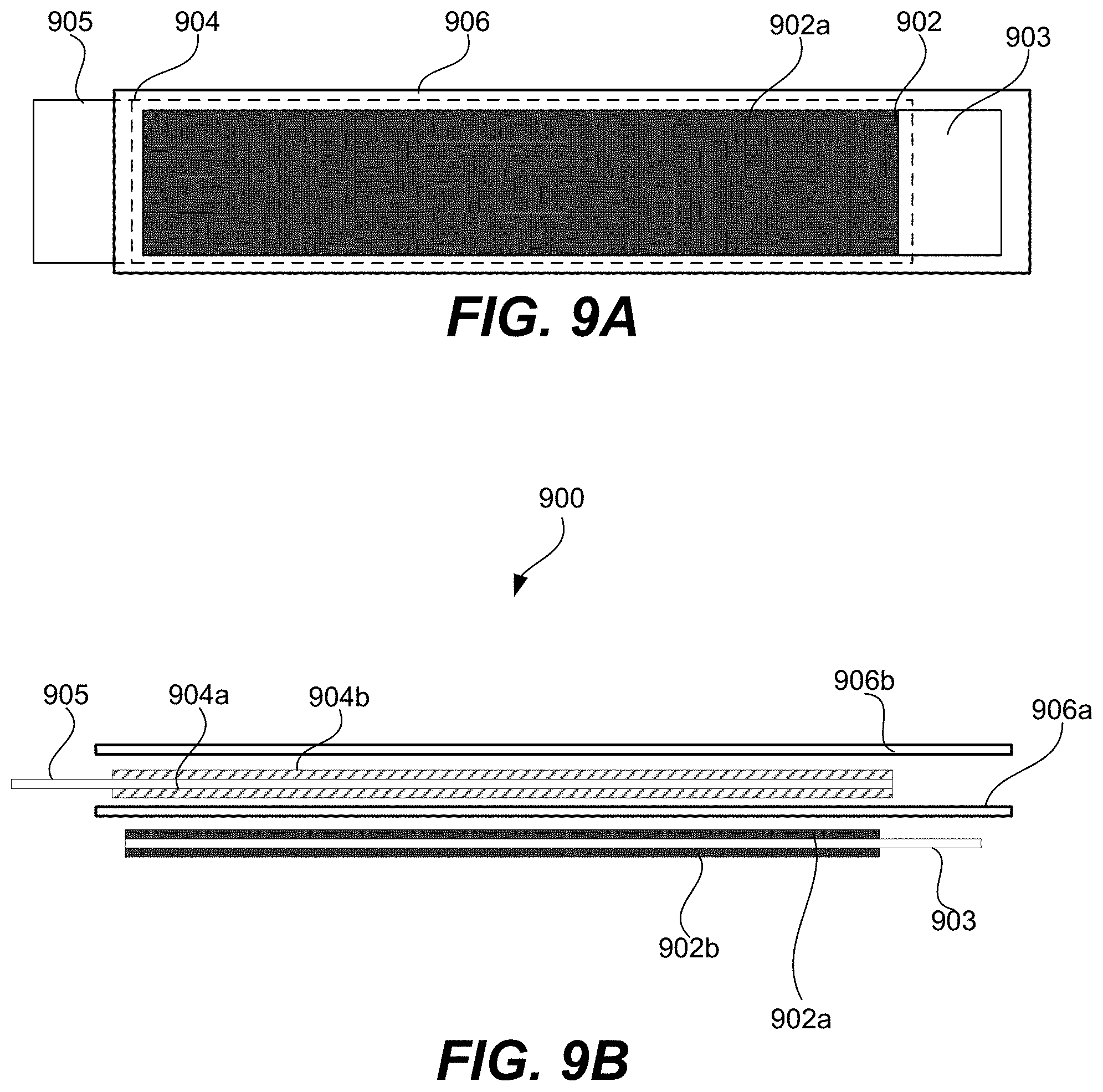
FIG. 9A is schematic representation of a plan view of a partially-assembled electrochemical cell that uses electrodes described herein, according to certain embodiments.
FIG. 9B is schematic representation of a cross-sectional view of an electrode stack of a partially-assembled electrochemical cell that uses electrodes described herein, according to certain embodiments.
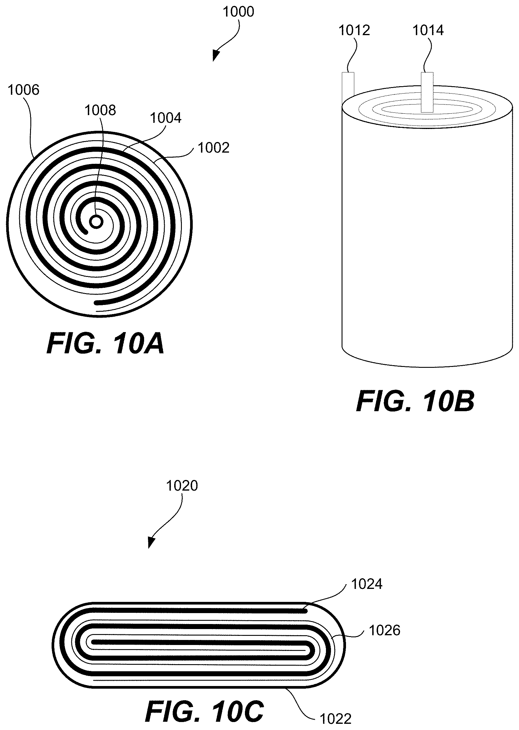
FIGS. 10A-10C are schematic representations of various views of electrodes wound together with two sheets of separator to form a cell according to certain embodiments.
FIGS. 11A and 11B are schematic representations of cross-sectional and perspective views of a stacked cell that includes a plurality of cells according to certain embodiments.
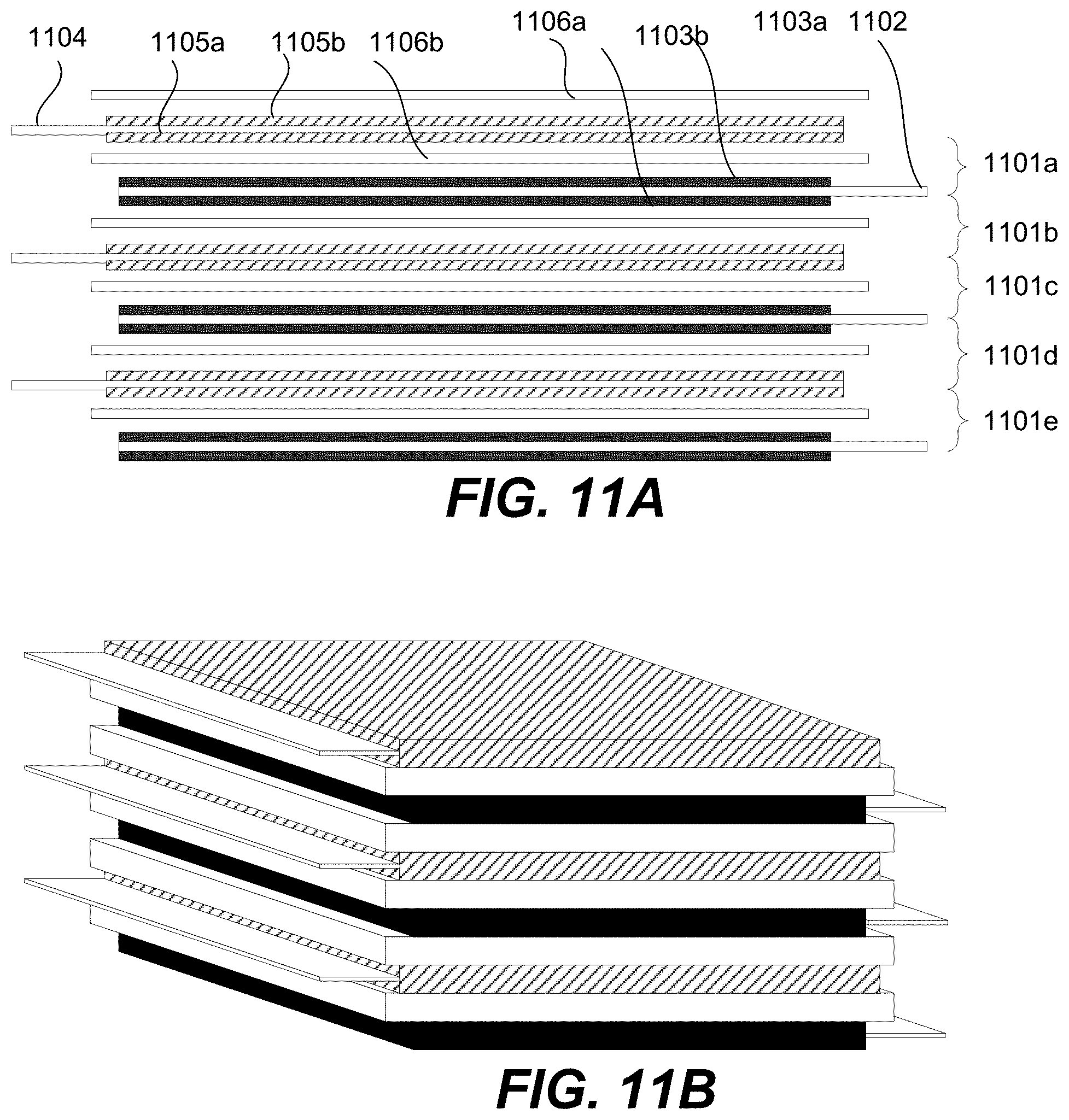
FIG. 12 is schematic representation of cross-sectional view of a wound cylindrical cell, in accordance with certain embodiments.
DETAILED DESCRIPTION
Certain embodiments are illustrated in the context of silicon deposition onto silicide nanowires. The skilled artisan will readily appreciate, however, that the materials and methods disclosed herein will have application in a number of other contexts where it is useful to adjust deposition to produce layers with specific characteristics. For example, various embodiments are described herein with reference to nanowires. It should be understood, however, that unless otherwise stated, the references herein to nanowires include other types of nanostructures as described in U.S. Pat. No. 8,257,866, incorporated by reference herein, such as nanotubes, nanoparticles, nanospheres, nanorods, nanowhiskers, and the like.
Generally, the term "nanostructures" refers to structures having at least one dimension that is less than about 1 micron. This dimension could be, for example, a diameter of the nanostructure (e.g., a silicide template nanowire), a thickness of the shell formed over a template (e.g., a thickness of the amorphous silicon layers), or some other nanostructure dimension. It should be understood that any of the overall dimensions (length and diameter) of the final coated structure do not have to be at a nanoscale. For example, a final structure may include a layer that is about 10 microns in thickness at its greatest diameter and coated over a template that is about 100 nanometers in diameter and 20 microns in length. While this overall structure is about 10.1 microns at its greatest diameter and 20 microns in length, it could be generally referred to as a "nanostructure" because of the dimensions of the template. In specific embodiments, the term "nanowire" refers to structures with nano-scaled shells positioned over elongated template structures.
Nanowires (as a specific case of nanostructures) have an aspect ratio of greater than one, typically at least about two and more frequently at least about four. In specific embodiments, nanowires have an aspect ratio of at least about 10 and even at least about 100 or 500. Nanowires may make use of their one larger dimension to connect to other electrode components (e.g., a conductive substrate, other active material structures, or conductive additives). For example, nanowires may be substrate rooted such that one end (or some other part) of the majority of the nanowires is in contact with the substrate. Because the two other dimensions are small and there is an adjacent void volume available for expansion, the internal stress built up in the nanowires during lithiation (e.g., expansion of the nano-shells positioned over the silicide templates) is also small and does not break apart the nanowires (as happens with larger structures). Certain dimensions of the nanowires (e.g., an overall diameter and/or a shell thickness) are kept below the corresponding fracture levels of the active material used. Nanowires also permit a relatively high capacity per unit area of the electrode surface due to their elongated structure, which corresponds to the height of the template structure. This results from their relatively high aspect ratio and terminal connection to the substrate.
Silicon nanostructures can be made by first growing a nanowire template structure that is not pure silicon and then coating the template with silicon. Thermal CVD (chemical vapor deposition), HWCVD (hot-wire CVD), and/or PECVD (plasma enhanced chemical vapor deposition) may be used to deposit the silicon.
Various deposition processes produce different profiles when depositing silicon onto nanowires. For example, thermal CVD creates a conformal amorphous Si coating. HWCVD (also known as catalytic CVD) makes a high density, non-conformal amorphous Si coating that is thicker at the tips of the nanowires and thinner at the roots of the nanowires near the substrate. PECVD also produces non-conformal amorphous Si coating that is thicker at the ends of the nanowires and thinner at the roots of the nanowires near the substrate, but the coating has a low density with many small voids.
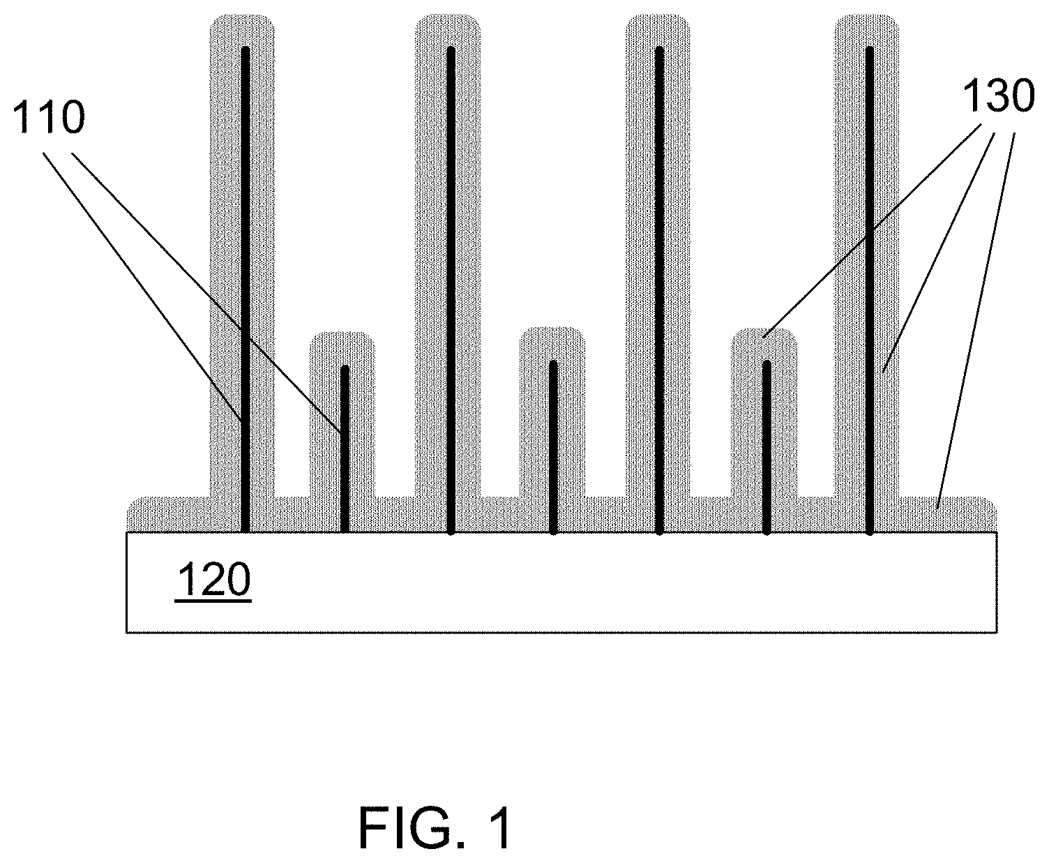
FIG. 1 is a schematic illustration of nanowires over which a conformal silicon layer has been deposited using thermal CVD. A nanowire template 110 is grown from a substrate 120. A silicon layer 130 is deposited onto the nanowire template 110. Note that the silicon layer 130 coats both the nanowire template 110 and the substrate 120, and that the coating has approximately the same thickness everywhere.
One advantage for the structure shown in FIG. 1 is that its structure is very dense. When an anode made using such a structure is cycled in a battery, the solid electrolyte interface (SEI) layer that forms on the silicon is very thin as the silicon formed by thermal CVD is very dense. One of the disadvantages for the structure shown in FIG. 1 is the thick layer of silicon at the roots of the nanowires. When an anode made using such a structure is cycled in a battery, there is great expansion and contraction in the silicon layer. Expansion in the root area can induce wrinkling of the Si layer and delamination of the nanowires, causing battery failure. Another disadvantage occurs because the nanowires in the template may not be exactly parallel as shown in FIG. 1. Instead, they grow at different angles and very often grow in clusters. The nanowires do not all have the same length. When coated by thermal CVD, the root area of the clusters, together with some short nanowires, can form a continuous silicon layer, which also can lead to delamination.
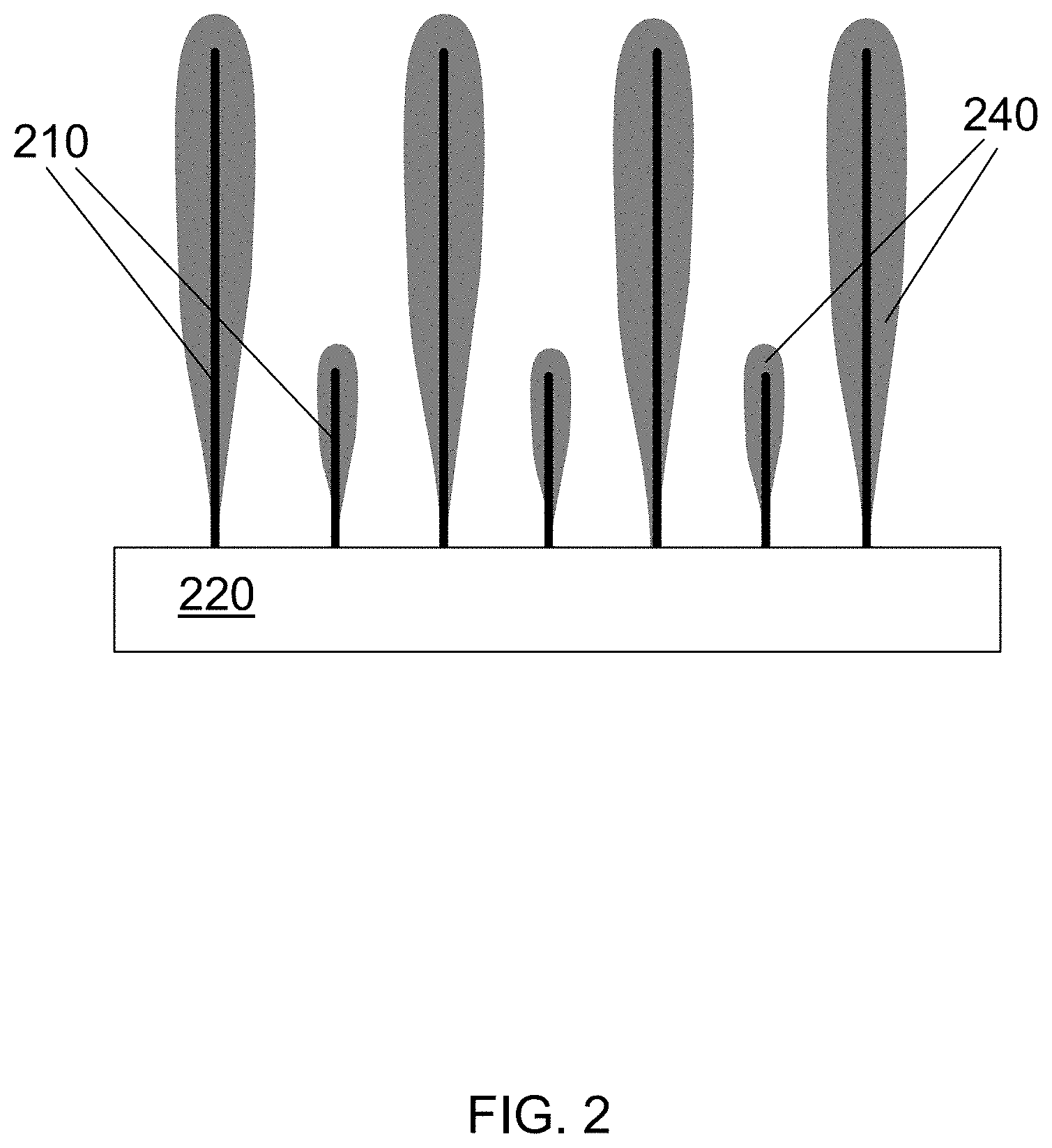
FIG. 2 is a schematic illustration of nanowires over which a silicon layer has been deposited using PECVD. Initially, PECVD may deposit a very thin layer (less than 1 micron and typically much less than 1 micron, such as 0.1-0.4 microns) of silicon on the substrate and at the roots of the nanowires. However, these areas are quickly shadowed by subsequent deposition at the tips of the nanowires. Depending on nanowire uniformity across the substrate surface, the very thin layer on the substrate may or may not be continuous. Under ideal surface and deposition conditions, a uniform thin layer may be expected but in practical cases, at the substrate-nanowire interface, there may be a discontinuity due to non-uniform distribution of nanowires on the surface.
In FIG. 2, a nanowire template 210 is grown from a substrate 220. A silicon layer 240 is deposited onto the nanowire template 210. Note that the silicon layer 240 is thickest at the tips of the nanowires of the nanowire template 210 and tapers off until there is essentially no silicon at the roots of nanowires. There is essentially no silicon on the substrate 220 either.
One advantage for the structure shown in FIG. 2 is that the root areas of the nanowires are coated only with only this very thin silicon layer. When an anode made using such a structure is cycled in a battery, the possibility of failure caused by expansion at the nanowire root area is greatly reduced. Another advantage is that PECVD coatings are not as dense as thermal CVD coatings; they can contain a large volume of voids and pores. Such defects can be very helpful in providing space into which the silicon can expand as it absorbs lithium.
One of the disadvantages of the structure shown in FIG. 2 is that the root area of the nanowires is not coated effectively. When an anode made using such a structure is cycled in a battery, the regions around the roots cannot participate electrochemically, thus causing a reduction in volumetric energy density of the battery. If more silicon were deposited onto the nanowires, the silicon layer at the tips of the nanowires would be too thick, causing fracturing of the silicon during cycling and subsequent anode failure. Another disadvantage is that the presence of voids can lead to large surface area of the coated nanowires and water absorption within the layer or at the surface. Very thick SEI layers can form as the battery is cycled, thus reducing the columbic efficiency and shortening the cycle life of the battery.
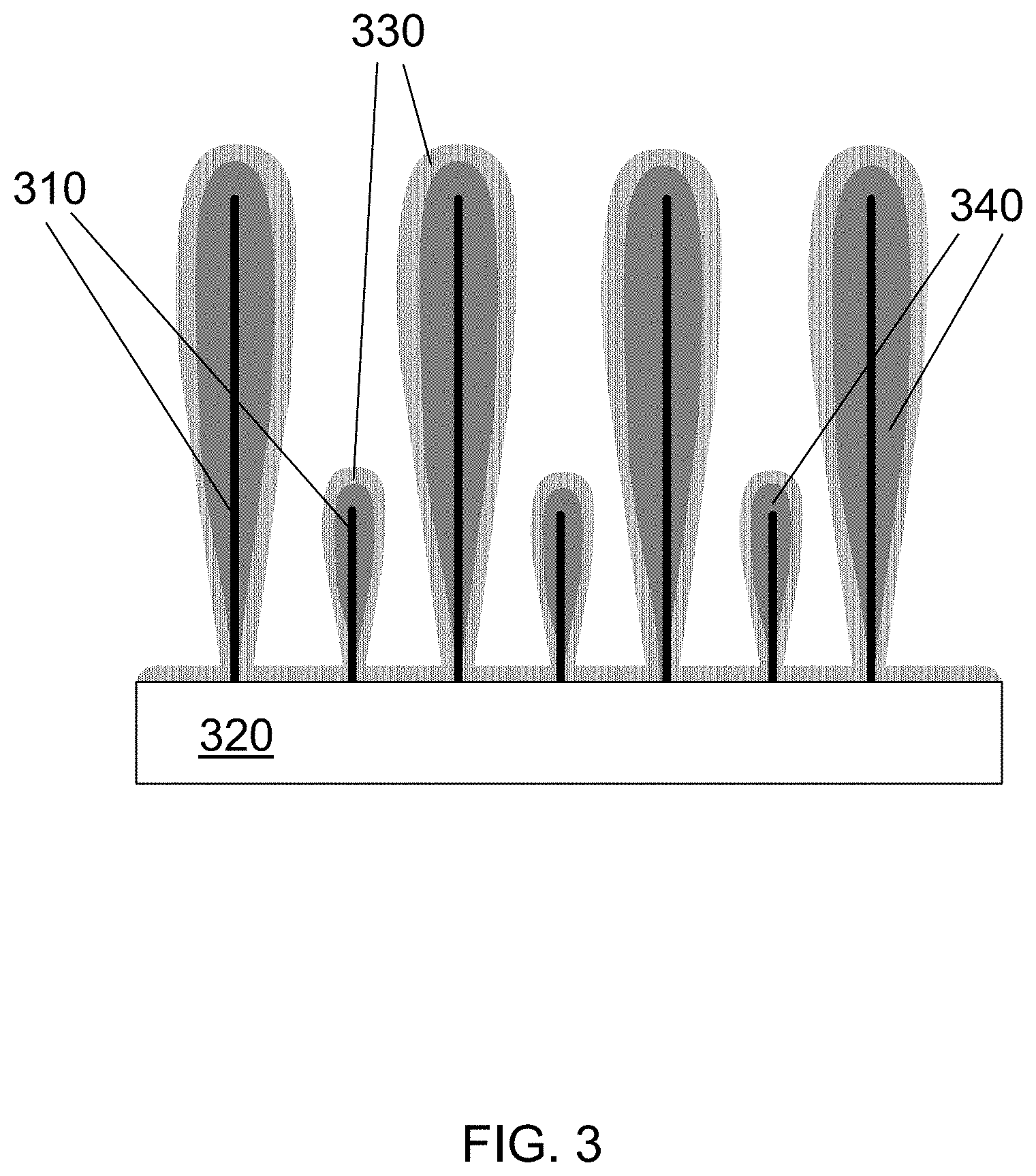
In one embodiment of the invention, the deposition methods discussed above are combined to provide optimum Si coatings as shown in FIG. 3 which is a schematic illustration of nanowires over which two silicon layers have been deposited. A nanowire template 310 is grown from a substrate 320. A first silicon layer 340 with a tapered profile is deposited onto the nanowire template 310 using PECVD. The first silicon layer 340 may be between about, for example, 0.5 and 10 microns thick at the top of the nanowire. In some embodiments, the first silicon layer may be thicker, e.g., between about 10 to 50 microns, or 10-20 microns. A second silicon layer 330 with a conformal profile is deposited onto the top of first silicon layer 340 using thermal CVD. The second silicon layer 330 may be, for example, between about 10 and 500 nm thick. The resulting structure has much more silicon at the tips of the nanowires than at the root ends. In more particular embodiments, the second silicon layer may be between 5 and 200 nm thick, or 10 to 90 nm thick. The second silicon layer 330 is conformal to the underlying surface, which includes the first silicon layer 340, the substrate 320, and any exposed portions of the nanowire template 310. As noted above, it has approximately uniform thickness.
According to various embodiments, the layer on the substrate surface may or may not be continuous. High performance may be achieved unless the layer on the substrate is too thick (e.g., greater than 2 microns) and continuous.
FIG. 4 is a SEM (scanning electron microscope) top-view image of nanowires over which a silicon layer has been deposited using PECVD.
FIG. 5 is a SEM top-view image of nanowires over which a first silicon layer has been deposited using PECVD and then a second silicon layer has been deposited using thermal CVD.
The novel structures described herein have many advantages. In some embodiments, there is more silicon near the tip of the nanowire than at the root, but there is still some silicon at the root. Having such a thin silicon layer at the root ensures that delamination does not occur during cycling. In some embodiments, there may also be electrochemical participation throughout the entire length of the nanowire. Further, SEI layer formation may be stabilized.
In some embodiments, the first silicon layer deposited is amorphous and has a low density, such as a density of about 1.70 g/cm.sup.3 or less, or 2.10 g/cm.sup.3 or less, or 2.2 g/cm.sup.3 or less, or less than 2.25 g/cm.sup.3 and may include many small voids. The second silicon layer deposited is amorphous and has a high density, such as a density of about 2.25 g/cm.sup.3 or more. The density of each layer is less than that of crystalline silicon.
According to various embodiments, the nanostructures may be characterized by a second silicon layer over a first silicon layer, the second silicon layer having a density higher than the density of the first silicon layer. As discussed above, in some embodiments, the first silicon layer provides space into which the silicon can expand as it absorbs lithium, while the second silicon layer reduces SEI layer formation. As such, the densities of each layer may be adjusted depending on the electrolyte, capacity of the battery, nanowire template density, etc. Accordingly, in some embodiments, the densities may be characterized in terms of a difference between densities of the layers, rather than or in addition to by absolute density. In some embodiments, the second silicon layer may have a density of at least 0.05 g/cm.sup.3 greater than the first silicon layer, or at least 0.1 g/cm.sup.3 greater than the first silicon layer, or at least 0.2 g/cm.sup.3 than the first silicon layer, or at least 0.3 g/cm.sup.3 greater than the first silicon layer.
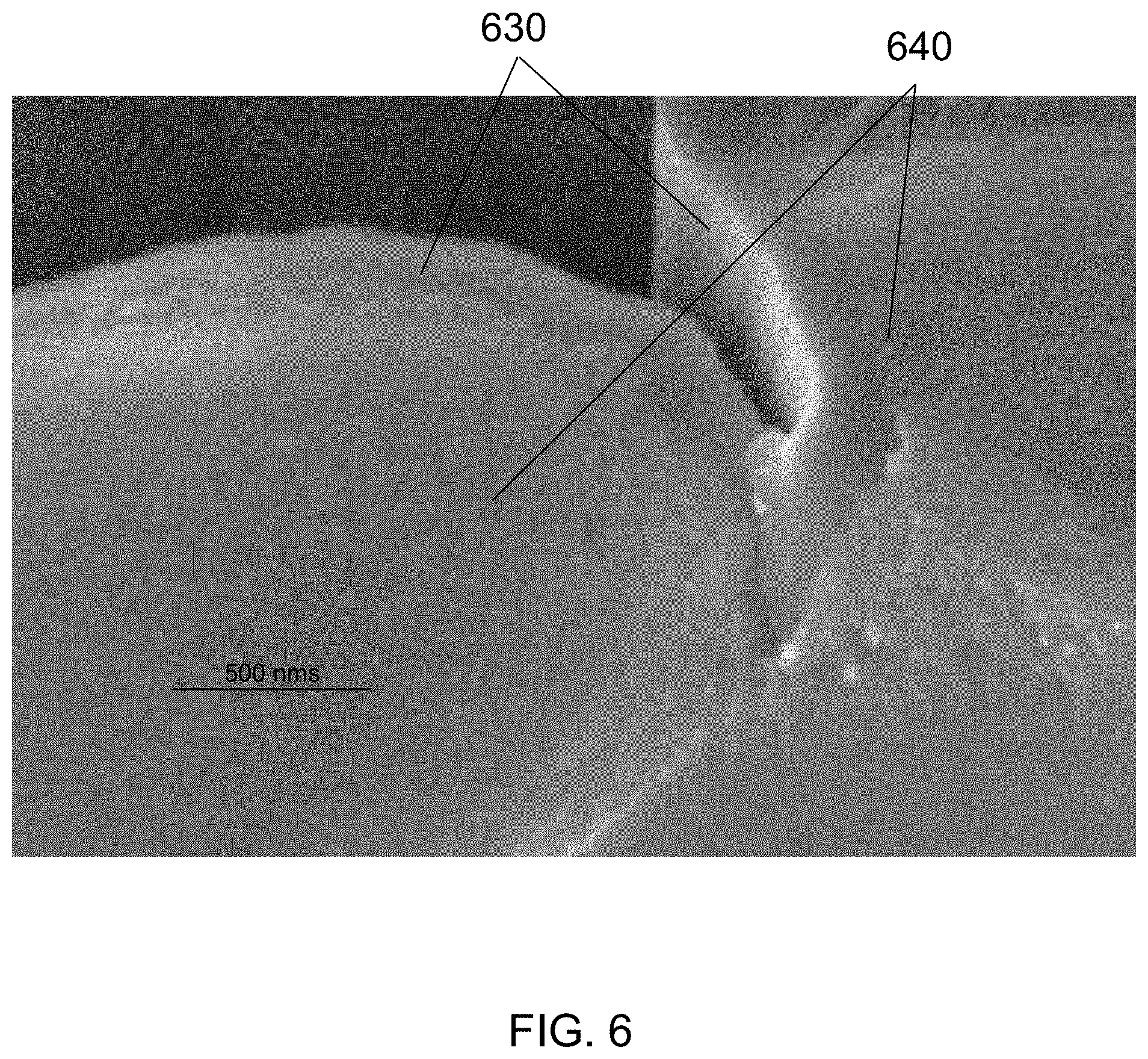
FIG. 6 is a SEM cross-section view image of a nanostructure that has an inner core of PECVD silicon 640 and an outer layer of thermal CVD silicon 630, according to an embodiment of the invention. The porous morphology of the PECVD silicon 640 can be seen clearly as can the non-porous morphology of the thermal CVD silicon 630.
Aspects of the methods and structures disclosed herein may be implemented with other high capacity active materials, in addition to or instead of silicon. An electrochemically active material may have a theoretical lithiation capacity of at least about 500 mAh/g or, more specifically, of at least about 1000 mAh/g. Active materials with such capacities may be referred to as "high capacity active materials." In addition to amorphous silicon, examples of high capacity active materials include silicon-containing compounds, tin and tin-containing compounds, germanium and germanium-containing compounds. For example, in some embodiments, an electrode may include a dual density germanium layer including a first inner layer having a lower density and second outer layer having a higher density.
In certain embodiments, high capacity active materials or templates are formed as substrate rooted nanostructures. These nanostructures may be physically and conductively attached to a conductive substrate, which may serve as a current collector for this electrode. The physical attachment may be more than a simple mechanical contact, which might result, for example, from coating a binder with discrete nanostructures onto the substrate. In some embodiments, the physical attachment results from fusion of the nanostructures to the substrate or deposition of the nanostructures or some portion of the nanostructures directly onto the substrate, for example, using CVD techniques or, even more, specifically using vapor-liquid-solid CVD growth. In yet another example, physical attachment results from ballistic impalement of the nanostructures onto the substrate. In certain embodiments, physical attachment includes certain forms of metallurgical bonds, such as a formation of alloys of two bonded materials (e.g., silicides).
In many embodiments, the nanowire template is a conductive material, with examples of conductive templates including metal templates and metal silicide templates. In some embodiments, a conductive template may include an oxide. As used herein, the term "conductive" refers broadly to electrical conductors, as distinct from semiconductors and insulators. The nanowire template may have conductivity of at least about 10.sup.3 S/m, or more specifically at least about 10.sup.6 S/m or even at least about 10.sup.7 S/m. Conductive templates can be useful to provide a transport path from the silicon electrochemically active material to a current collector as well as mechanically supporting the silicon layers. In some embodiments, however, the nanowire template may be a semiconductor or insulator (e.g., an oxide) that provides mechanical support to the silicon. Silicon nanowires may also be used as a template, with one or more coatings of a-Si deposited over the silicon nanowires as described herein. Silicon nanowire anodes are described in U.S. Pat. No. 7,816,031, incorporated by reference herein.
Nanowires of the nanowire template may be non-branched linear nanowires or branched nanowires. An electrode may include a combination of non-branched and branched nanowires, or only include only one of these types. While the templates may generally be elongated template structures, as described above, nanospheres, nanorods, nanowhiskers, nanoparticles, and the like may be employed. A nanowire template may be part of or include a multidimensional structure. One example of such a structure is a central core to which multiple nanowires are attached, forming "fuzzy ball-like" or "snowball-like" structures. An example of such a structure is shown in U.S. patent application Ser. No. 13/277,821, incorporated by reference herein.
In certain embodiments, nanowires in a nanowire template are between about 10 nanometers and 100 nanometers in diameter and between about 10 microns and 100 microns in length. In one example, a structure may include nanowires ranging from 5 to 40 microns. However, nanowires having other dimensions may be used.
Nanowire density can depend on the length of the nanowires, the desired capacity, the expansion ratio of the active material, and the particular application. If spacing between template structures is less than the coating thickness, it can cause significant interconnections of the active material layer. Interconnections near the roots can create agglomerated or continuous film like structures, which impede good cycle performance. The nanowires may be randomly distributed, with a variety of lengths and randomly-oriented. In some implementations, however, templated or guided methods of growth that produce uniform densities and/or orientations may be used. In one example, nanowires of a template structure may be grouped into various size bins, e.g., short, medium, and long sizes. Long nanowires may be identified as being visible in a top-down SEM image as depicted above. Example densities may be 0.5 to 20 long nanowires per 100 micron squared and 2 to 400 total nanowires per 100 microns squared. In some embodiments, a nanowire density may be determined for a particular mass loading. For example, for a mass loading between 2.5 and 2.9 mg/cm.sup.2, a top diameter of the Si coating of 4 to 6 microns and a bottom diameter of 0.2 to 0.3 microns, a top nanowire density may be 2.times.10.sup.6 to 6.times.10.sup.6 long nanowires per centimeter squared.
The substrate is generally a conductive material having a conductivity of at least about 10.sup.3 S/m, or more specifically at least about 10.sup.6 S/m or even at least about 10.sup.7 S/m, particularly if the nanowire template is rooted to the substrate, and may be used as a current collector in the battery. This may be desirable when the substrate rooted structure is employed as a fully fabricated electrode for a battery or fuel cell. Examples of conductive substrate materials include copper, copper coated with metal oxides, stainless steel, titanium, aluminum, nickel, chromium, tungsten, other metals, metal silicides and other conductive metal compounds, carbon, carbon fiber, graphite, graphene, carbon mesh, conductive polymers, doped silicon or combinations of above including multi-layer structures. The substrate may be formed as a foil, film, mesh, foam, laminate, wires, tubes, particles, multi-layer structure, or any other suitable configuration. In certain embodiments, a substrate is a metallic foil with a thickness of between about 1 micron and 50 microns or more specifically between about 5 microns and 30 microns.
According to various embodiments, a silicon coating may be characterized by one or more of shape (also referred to as morphology), density, and bulk and surface composition. In terms of morphology, the first silicon layer may be generally characterized as non-conformal, having a thickness that is variable in the direction vertical to the substrate.
In some embodiments, a silicon layer has a generally circular symmetry. See, e.g., the top view SEM image in FIG. 4. It should be noted that an array of nanowires having generally circular symmetry includes arrays in which asymmetries may be introduced due to two nanowires being close enough that their coatings abut one another.
FIG. 7 shows a schematic depiction of a representation of a coating as a water drop or a conical frustum. The dimensions d1, d2 and h are labeled, with d1 being the largest diameter of the coating, d2 being the bottom diameter of the coating, and h being the height of the anode after coating. The non-conformal coating (porous non-conformal coating alone, or porous non-conformal coating conformally coated with the dense coating) may be characterized in some embodiments by the following ratios: d1/h of 1/2 to 1/9, d2/h of 1/400 to 1/70 and a d1/d2 ratio of 50:1 to 1.5:1.
In an example, d1 may be between 4 and 15 microns, or 4 and 12 microns, d2 may be between about 0.2 and 2 microns, and height may be between about 20 and 50 microns, e.g., between about 30 and 40 microns. The coating may extend between 10 and 20 microns above the height of the nanowire in some embodiments. The non-conformal layer substantially coats the nanowire, with the non-conformal coating extending at least most of the length of the nanowires, and in some embodiments, coating the entire template. As described above, there may be discontinuities near or at the root of the nanowire template.
In one example, a nanowire having a diameter of about 10 to 50 nm and a length of between about 10 to 25 microns is coated with silicon, such that after coating the diameter of the nanostructure at the root is 100 to 400 nm, the maximum diameter is 2 to 20 microns, and the total height of the anode is 20 to 40 microns.
In some embodiments, a non-conformal layer may be characterized by a hydrogen (H) content of at least 10%. In some embodiments, a conformal, dense layer may be characterized by a bulk H content of no more than 7%, or no more than 5%.
The non-conformal, porous silicon layers may be deposited by a method such as evaporation or other physical vapor deposition (PVD) method or HWCVD instead of or in addition to PECVD.
In PECVD processes, according to various implementations, a plasma may be generated in a chamber in which the substrate is disposed or upstream of the chamber and fed into the chamber. Any type of plasma, including capacitively-coupled plasmas, inductively-coupled plasmas, and conductive coupled plasmas may be used. Any appropriate plasma source may be used, including DC, AC, RF and microwave sources may be used.
PECVD process conditions can vary according to the particular process and tool used. A fairly wide range of temperatures, e.g., 180.degree. C. to 600.degree. C., may be used. Pressures are generally low for plasma processes, e.g., ranging from 50 mTorr to 400 Torr, or 200 mTorr to 10 Torr, depending on the process.
In some implementations, the PECVD process is an expanding thermal plasma chemical vapor deposition (ETP-CVD) process. In such a process, a plasma generating gas is passed through a direct current arc plasma generator to form a plasma, with a web or other substrate including the nanowire template in an adjoining vacuum chamber. A silicon source gas is injected into the plasma, with radicals generated. The plasma is expanded via a diverging nozzle and injected into the vacuum chamber and toward the substrate, with a non-conformal layer of amorphous silicon formed on the nanowire template. An example of a plasma generating gas is argon (Ar). In some embodiments, the ionized argon species in the plasma collide with silicon source molecules to form radical species of the silicon source, resulting in deposition on the nanowire template. Example ranges for voltages and currents for the DC plasma source are 60 to 80 volts and 50 to 70 amperes, respectively.
The conformal, dense silicon layers may be deposited by a method as atomic layer deposition (ALD) instead of or in addition to thermal CVD. Any appropriate thermal CVD process may be used, such as low pressure CVD (LPCVD). Temperatures may go as high as the thermal budget allows in some embodiments, as long as no metal silicide is formed around nanowire-substrate interface due to the increase of temperature when using a metal substrate.
Any appropriate silicon source may be used for the non-conformal and conformal silicon layers, including silane (SiH.sub.4), dichlorosilane (H.sub.2SiCl.sub.2), monochlorosilane (H.sub.3SiCl), trichlorosilane (HSiCl.sub.3), and silicon tetrachloride (SiCl.sub.4) to form the silicon layers. Depending on the gas used, the amorphous silicon layer may be formed by decomposition or a reaction with another compound, such as by hydrogen reduction. According to various embodiments, the same or a different silicon source may be used for the each of the layers.
According to various embodiments, the PECVD processes result in non-conformal coatings due to gas phase radical generation of the silicon precursor and gas phase nucleation and condensation on the surfaces of the template. By contrast, the thermal CVD reactions are run at conditions that result in surface reactions. High energy and mobility at the surface results in a conformal layer. In some embodiments, chamber pressure during a thermal CVD process is kept low, e.g., 100 mTorr to 2 Torr to prevent gas phase reactions and non-conformal deposition. Higher pressures, e.g., higher than 2 Torr or 500 Torr can result in non-conformal deposition.
Additional description of depositing active material layers having controlled densities may be found in U.S. patent application Ser. No. 13/277,821, incorporated by reference herein.
As indicated above, the nanostructures may be characterized by a second silicon layer over a first silicon layer, the second silicon layer having a density higher than the density of the first silicon layer. In some embodiments, the first silicon layer may be deposited directly on the nanowire template, with the second silicon layer being the outermost shell of the coated template. However, in some embodiments, other layers may be present. For example, a thin dense silicon layer may be deposited on a nanowire template, followed by a thicker porous layer, and a second thin dense layer.
Still further, a non-Si layer may be the outermost shell of the nanostructure in some embodiments. Examples of layers include metal oxides such as aluminum oxide, titanium oxide, cobalt oxide, and zirconium oxide, metal nitrides, and silicon nitrides. In some embodiments, a thin layer of any of these may be deposited in addition to or instead of the dense Si layer described above.
According to various embodiments, each of the first and second silicon layers may have a uniform density. However, in some embodiments, deposition conditions may be tuned during deposition to provide a density gradient in one or both layers. For example, either layer may get denser toward the outer part of the layer. In such embodiments, an average density of the layer may be used to characterize the density of layer as described above.
In some embodiments, silicon may be deposited by HWCVD. In some such implementations, a single Si layer having a density between that typically deposited by PECVD and that typically deposited by TCVD may be deposited. It can also be used to coat both the first and the second Si coatings by tuning the deposition process.
Experimental
Cycling data from nanowires with two layers of Si as described herein, shows that such structures have increased cycle lifetimes over structures that are made using only PECVD or only thermal CVD. FIGS. 8A and 8B are graphs shown capacity vs. cycle number and capacity retention vs. cycle number for electrodes having templated PECVD+thermal CVD (TCVD) Si layers, templated PECVD only Si layers, and template TCVD only layers. Capacity and capacity retention is highest for the PECVD+TCVD Si layers. As described above, the PECVD layer is a more porous, less dense internal layer and the TCVD layer is a denser external layer.
Assembly
FIG. 9A is a plan view of a partially-assembled electrochemical cell that uses electrodes described herein, according to certain embodiments. The cell has a positive electrode active layer 902 that is shown covering a major portion of a positive current collector 903. The cell also has a negative electrode active layer 904 that is shown covering a major portion of a negative current collector 905. Separator 906 is between the positive electrode active layer 902 and the negative electrode active layer 904.
In one embodiment, the negative electrode active layer 904 is slightly larger than the positive electrode active layer 902 to ensure trapping of the lithium ions released from the positive e
References
D00001
D00002
D00003
D00004
D00005
D00006
D00007
D00008
D00009
D00010
D00011
D00012
XML
uspto.report is an independent third-party trademark research tool that is not affiliated, endorsed, or sponsored by the United States Patent and Trademark Office (USPTO) or any other governmental organization. The information provided by uspto.report is based on publicly available data at the time of writing and is intended for informational purposes only.
While we strive to provide accurate and up-to-date information, we do not guarantee the accuracy, completeness, reliability, or suitability of the information displayed on this site. The use of this site is at your own risk. Any reliance you place on such information is therefore strictly at your own risk.
All official trademark data, including owner information, should be verified by visiting the official USPTO website at www.uspto.gov. This site is not intended to replace professional legal advice and should not be used as a substitute for consulting with a legal professional who is knowledgeable about trademark law.