Method and apparatus for infrared detection and display
So
U.S. patent number 10,700,141 [Application Number 11/865,505] was granted by the patent office on 2020-06-30 for method and apparatus for infrared detection and display. This patent grant is currently assigned to University of Florida Research Foundation, Incorporated. The grantee listed for this patent is Franky So. Invention is credited to Franky So.


| United States Patent | 10,700,141 |
| So | June 30, 2020 |
Method and apparatus for infrared detection and display
Abstract
Embodiments of the subject invention relate to a method and apparatus for infrared (IR) detection. Organic layers can be utilized to produce a phototransistor for the detection of IR radiation. The wavelength range of the IR detector can be modified by incorporating materials sensitive to photons of different wavelengths. Quantum dots of materials sensitive to photons of different wavelengths than the host organic material of the absorbing layer of the phototransistor can be incorporated into the absorbing layer so as to enhance the absorption of photons having wavelengths associated with the material of the quantum dots. A photoconductor structure can be used instead of a phototransistor. The photoconductor can incorporate PbSe or PbS quantum dots. The photoconductor can incorporate organic materials and part of an OLED structure. A detected IR image can be displayed to a user. Organic materials can be used to create an organic light-emitting device.
| Inventors: | So; Franky (Gainesville, FL) | ||||||||||
|---|---|---|---|---|---|---|---|---|---|---|---|
| Applicant: |
|
||||||||||
| Assignee: | University of Florida Research
Foundation, Incorporated (Gainesville, FL) |
||||||||||
| Family ID: | 39269145 | ||||||||||
| Appl. No.: | 11/865,505 | ||||||||||
| Filed: | October 1, 2007 |
Prior Publication Data
| Document Identifier | Publication Date | |
|---|---|---|
| US 20100181552 A1 | Jul 22, 2010 | |
Related U.S. Patent Documents
| Application Number | Filing Date | Patent Number | Issue Date | ||
|---|---|---|---|---|---|
| 60930225 | May 14, 2007 | ||||
| 60848581 | Sep 29, 2006 | ||||
| Current U.S. Class: | 1/1 |
| Current CPC Class: | H01L 27/288 (20130101); H01L 27/3227 (20130101); H01L 51/4213 (20130101); H01L 51/428 (20130101); H01L 27/307 (20130101); Y02E 10/52 (20130101); Y02E 10/549 (20130101); H01L 51/0053 (20130101); Y02P 70/521 (20151101); Y02P 70/50 (20151101); H01L 51/0081 (20130101); H01L 51/0504 (20130101) |
| Current International Class: | H01L 31/00 (20060101); H01L 27/32 (20060101); H01L 27/28 (20060101); H01L 27/30 (20060101); H01L 51/42 (20060101); H01L 51/00 (20060101); H01L 51/05 (20060101) |
| Field of Search: | ;257/270,286,365,401,E29.023,E29.027,E29.04,E29.117,E29.12,E29.122,E29.134,E29.136,E29.264,E29.275 |
References Cited [Referenced By]
U.S. Patent Documents
| 4614958 | September 1986 | Mikami |
| 4679063 | July 1987 | White |
| 4755674 | July 1988 | Schaaf |
| 4778692 | October 1988 | Ishihara |
| 4885211 | December 1989 | Tang et al. |
| 5121398 | June 1992 | Rao |
| 5122905 | June 1992 | Wheatley et al. |
| 5270092 | December 1993 | Griffith et al. |
| 5315129 | May 1994 | Forrest et al. |
| 5336578 | August 1994 | Nukada et al. |
| 5389788 | February 1995 | Grinberg et al. |
| 5438198 | August 1995 | Ebitani et al. |
| 5619039 | April 1997 | Montanari |
| 5710428 | January 1998 | Ko |
| 5811834 | September 1998 | Tamano et al. |
| 5965875 | October 1999 | Merrill |
| 6097147 | August 2000 | Baldo et al. |
| 6140646 | October 2000 | Busta et al. |
| 6337492 | January 2002 | Jones et al. |
| 6509574 | January 2003 | Yuan et al. |
| 6579629 | June 2003 | Raychaudhuri et al. |
| 6734452 | May 2004 | Gunapala et al. |
| 6777961 | August 2004 | Hamamoto et al. |
| 6906326 | June 2005 | Koch et al. |
| 6914315 | July 2005 | Lai et al. |
| 6972431 | December 2005 | Forrest et al. |
| 7247850 | July 2007 | Laou |
| 7270586 | September 2007 | Tokailin et al. |
| 7279705 | October 2007 | Iou |
| 7300731 | November 2007 | Wang |
| 8304728 | November 2012 | So |
| 8405028 | March 2013 | So |
| 8441187 | May 2013 | Hunze et al. |
| 8507865 | August 2013 | Boberl et al. |
| 8592801 | November 2013 | So et al. |
| 8716701 | May 2014 | So et al. |
| 8796699 | August 2014 | So et al. |
| 8829498 | September 2014 | So et al. |
| 9006752 | April 2015 | So et al. |
| 9054262 | June 2015 | Lewis et al. |
| 9196661 | November 2015 | So et al. |
| 9214502 | December 2015 | So et al. |
| 9276048 | March 2016 | So |
| 10134815 | November 2018 | So et al. |
| 2002/0027206 | March 2002 | Yuan et al. |
| 2002/0066904 | June 2002 | Yuan |
| 2002/0130248 | September 2002 | Bretschneider et al. |
| 2003/0122749 | July 2003 | Booth et al. |
| 2003/0218166 | November 2003 | Tsutsui |
| 2004/0016923 | January 2004 | Yu et al. |
| 2004/0027059 | February 2004 | Tsutsui |
| 2004/0031965 | February 2004 | Forrest |
| 2004/0121568 | June 2004 | Kim |
| 2004/0135222 | July 2004 | Robert et al. |
| 2004/0222306 | November 2004 | Fajarillo |
| 2004/0253759 | December 2004 | Garber et al. |
| 2004/0262614 | December 2004 | Hack et al. |
| 2005/0077539 | April 2005 | Lipson |
| 2005/0088079 | April 2005 | Daniels |
| 2005/0088365 | April 2005 | Yamazaki et al. |
| 2005/0104089 | May 2005 | Engelmann et al. |
| 2005/0110007 | May 2005 | Forrest et al. |
| 2005/0126628 | June 2005 | Scher et al. |
| 2005/0137301 | June 2005 | Wu et al. |
| 2005/0155641 | July 2005 | Fafard |
| 2005/0156609 | July 2005 | Pfaff et al. |
| 2005/0161703 | July 2005 | Costello |
| 2005/0168137 | August 2005 | Adamovich et al. |
| 2005/0236556 | October 2005 | Sargent |
| 2006/0011927 | January 2006 | Ko |
| 2006/0024526 | February 2006 | Thompson et al. |
| 2006/0032528 | February 2006 | Wang |
| 2006/0043361 | March 2006 | Lee et al. |
| 2006/0081840 | April 2006 | Mori et al. |
| 2006/0084347 | April 2006 | Tutt et al. |
| 2006/0097247 | May 2006 | Kim |
| 2006/0157806 | July 2006 | Rhodes |
| 2006/0180197 | August 2006 | Gui et al. |
| 2006/0186803 | August 2006 | Lim et al. |
| 2006/0192125 | August 2006 | Yoganandan et al. |
| 2006/0222979 | October 2006 | Ishida et al. |
| 2006/0227531 | October 2006 | Iou |
| 2006/0266998 | November 2006 | Vega |
| 2006/0290270 | December 2006 | Kim et al. |
| 2007/0048548 | March 2007 | Kim et al. |
| 2007/0051876 | March 2007 | Sumi et al. |
| 2007/0062576 | March 2007 | Duerr et al. |
| 2007/0096085 | May 2007 | Rand et al. |
| 2007/0102694 | May 2007 | Drndic et al. |
| 2007/0116983 | May 2007 | Kanno et al. |
| 2007/0129545 | June 2007 | Inoue et al. |
| 2007/0176541 | August 2007 | Son et al. |
| 2007/0215868 | September 2007 | Forrest et al. |
| 2007/0216985 | September 2007 | Woodall et al. |
| 2007/0221888 | September 2007 | Sakata |
| 2007/0235753 | October 2007 | Debucquoy et al. |
| 2008/0041447 | February 2008 | Tseng et al. |
| 2008/0066802 | March 2008 | Reddy |
| 2008/0078444 | April 2008 | Atanackovic |
| 2008/0110499 | May 2008 | Chen et al. |
| 2008/0138797 | June 2008 | Hunt et al. |
| 2008/0142075 | June 2008 | Reddy et al. |
| 2008/0223445 | September 2008 | Marks et al. |
| 2008/0230120 | September 2008 | Reddy |
| 2008/0272713 | November 2008 | Kang et al. |
| 2009/0045728 | February 2009 | Murano et al. |
| 2009/0115310 | May 2009 | Yamamoto |
| 2009/0140238 | June 2009 | Brabec et al. |
| 2009/0152664 | June 2009 | Klem et al. |
| 2009/0206745 | August 2009 | Hwang et al. |
| 2009/0208776 | August 2009 | Liu et al. |
| 2009/0214967 | August 2009 | Iwanaga et al. |
| 2009/0217967 | September 2009 | Hovel et al. |
| 2009/0223566 | September 2009 | Mitsui et al. |
| 2009/0286338 | November 2009 | Coe-Sullivan et al. |
| 2009/0301556 | December 2009 | Kawano et al. |
| 2009/0321726 | December 2009 | Thompson |
| 2010/0025662 | February 2010 | Cho et al. |
| 2010/0044676 | February 2010 | Sargent et al. |
| 2010/0044767 | February 2010 | Chaudhry et al. |
| 2010/0059097 | March 2010 | McDonald et al. |
| 2010/0116995 | May 2010 | Levene et al. |
| 2010/0133418 | June 2010 | Sargent et al. |
| 2010/0133434 | June 2010 | Meng et al. |
| 2010/0133522 | June 2010 | Pieh et al. |
| 2010/0141122 | June 2010 | Begley et al. |
| 2010/0229921 | September 2010 | Farris et al. |
| 2010/0233842 | September 2010 | Grein et al. |
| 2010/0243053 | September 2010 | Coe-Sullivan et al. |
| 2010/0255601 | October 2010 | Beaudet |
| 2010/0282309 | November 2010 | Pschirer et al. |
| 2010/0294936 | November 2010 | Boeberl et al. |
| 2010/0302419 | December 2010 | Den Boer et al. |
| 2010/0326506 | December 2010 | Lifshitz et al. |
| 2011/0012091 | January 2011 | Forrest et al. |
| 2011/0031399 | February 2011 | So |
| 2011/0031403 | February 2011 | So |
| 2011/0049489 | March 2011 | Forrest et al. |
| 2011/0068330 | March 2011 | Akimoto et al. |
| 2011/0073835 | March 2011 | Ren et al. |
| 2011/0079706 | April 2011 | Michalewicz |
| 2011/0114921 | May 2011 | Yang et al. |
| 2011/0116078 | May 2011 | Cho et al. |
| 2011/0140075 | June 2011 | Zhou et al. |
| 2011/0248249 | October 2011 | Forrest et al. |
| 2011/0303906 | December 2011 | Goldman |
| 2012/0068140 | March 2012 | Greenham et al. |
| 2012/0126204 | May 2012 | So et al. |
| 2012/0187295 | July 2012 | So et al. |
| 2012/0193689 | August 2012 | Park et al. |
| 2012/0241723 | September 2012 | Klem et al. |
| 2012/0286296 | November 2012 | So et al. |
| 2013/0044250 | February 2013 | Senda et al. |
| 2013/0206988 | August 2013 | So |
| 2013/0215496 | August 2013 | Ban et al. |
| 2014/0054540 | February 2014 | Thou et al. |
| 2014/0060613 | March 2014 | So et al. |
| 2014/0111652 | April 2014 | So et al. |
| 2014/0217284 | August 2014 | So et al. |
| 2014/0326921 | November 2014 | Lu et al. |
| 2014/0353502 | December 2014 | So et al. |
| 2014/0367572 | December 2014 | So et al. |
| 2015/0001395 | January 2015 | So et al. |
| 2015/0151980 | June 2015 | Tisdale et al. |
| 2015/0372046 | December 2015 | Kim et al. |
| 2017/0117335 | April 2017 | So et al. |
| 2019/0006541 | January 2019 | So et al. |
| 1532959 | Sep 2004 | CN | |||
| 1637628 | Jul 2005 | CN | |||
| 1773732 | May 2006 | CN | |||
| 1806343 | Jul 2006 | CN | |||
| 1856888 | Nov 2006 | CN | |||
| 101340749 | Jan 2009 | CN | |||
| 101405888 | Apr 2009 | CN | |||
| 101421664 | Apr 2009 | CN | |||
| 101558348 | Oct 2009 | CN | |||
| 101794834 | Aug 2010 | CN | |||
| 101872793 | Oct 2010 | CN | |||
| 102725616 | Oct 2012 | CN | |||
| 0 508 970 | Oct 1992 | EP | |||
| 0 848 433 | Jun 1998 | EP | |||
| 0 569 257 | Jun 2002 | EP | |||
| 1 351 558 | Oct 2003 | EP | |||
| 1 498 960 | Jan 2005 | EP | |||
| S58-215081 | Dec 1983 | JP | |||
| S60-030163 | Feb 1985 | JP | |||
| S61-149831 | Jul 1986 | JP | |||
| S63-088872 | Apr 1988 | JP | |||
| S64-012583 | Jan 1989 | JP | |||
| H02-016421 | Jan 1990 | JP | |||
| H02-224279 | Sep 1990 | JP | |||
| H03-079693 | Apr 1991 | JP | |||
| H04-204333 | Jul 1992 | JP | |||
| H07-122762 | May 1995 | JP | |||
| 7175420 | Jul 1995 | JP | |||
| H08-007096 | Jan 1996 | JP | |||
| H10-065200 | Mar 1998 | JP | |||
| H10-242493 | Sep 1998 | JP | |||
| H11-329736 | Nov 1999 | JP | |||
| 2000-277265 | Oct 2000 | JP | |||
| 2000-349365 | Dec 2000 | JP | |||
| 2001-006876 | Jan 2001 | JP | |||
| 2001-076882 | Mar 2001 | JP | |||
| 2002-523904 | Jul 2002 | JP | |||
| 2002-340668 | Nov 2002 | JP | |||
| 2003-083809 | Mar 2003 | JP | |||
| 2003-178887 | Jun 2003 | JP | |||
| 2004-511911 | Apr 2004 | JP | |||
| 2005-522005 | Jul 2005 | JP | |||
| 2005-266537 | Sep 2005 | JP | |||
| 2005-277113 | Oct 2005 | JP | |||
| 2006-013103 | Jan 2006 | JP | |||
| 2006-066395 | Mar 2006 | JP | |||
| 2006-128437 | May 2006 | JP | |||
| 2006-518110 | Aug 2006 | JP | |||
| 2006-251555 | Sep 2006 | JP | |||
| 2007-519237 | Jul 2007 | JP | |||
| 2008-016831 | Jan 2008 | JP | |||
| 2008-053736 | Mar 2008 | JP | |||
| 2008-523615 | Jul 2008 | JP | |||
| 2009-509129 | Mar 2009 | JP | |||
| 2009-520358 | May 2009 | JP | |||
| 2009-527108 | Jul 2009 | JP | |||
| 2009-192919 | Aug 2009 | JP | |||
| 2009-531837 | Sep 2009 | JP | |||
| 2009-253173 | Oct 2009 | JP | |||
| 2009-272528 | Nov 2009 | JP | |||
| 2010-506386 | Feb 2010 | JP | |||
| 2010-067642 | Mar 2010 | JP | |||
| 2010-067802 | Mar 2010 | JP | |||
| 2010-087205 | Apr 2010 | JP | |||
| 2010-192931 | Sep 2010 | JP | |||
| 2010-263030 | Nov 2010 | JP | |||
| 2010-534409 | Nov 2010 | JP | |||
| 2011-098948 | May 2011 | JP | |||
| 2012-524991 | Oct 2012 | JP | |||
| 2013-512439 | Apr 2013 | JP | |||
| 2014-511041 | May 2014 | JP | |||
| 1020090080056 | Jul 2009 | KR | |||
| 200637425 | Oct 2006 | TW | |||
| 200847449 | Dec 2008 | TW | |||
| 201041203 | Nov 2010 | TW | |||
| WO 02/099896 | Dec 2002 | WO | |||
| WO-2003/084292 | Oct 2003 | WO | |||
| WO-2004/073082 | Aug 2004 | WO | |||
| WO 2005/069387 | Jul 2005 | WO | |||
| WO-2005-101530 | Oct 2005 | WO | |||
| WO 2006/130717 | Dec 2006 | WO | |||
| WO 2007/017475 | Feb 2007 | WO | |||
| WO 2007/095386 | Aug 2007 | WO | |||
| WO 2007/102051 | Sep 2007 | WO | |||
| WO 2007/131126 | Nov 2007 | WO | |||
| WO 2008/042859 | Apr 2008 | WO | |||
| WO 2008/054845 | May 2008 | WO | |||
| WO 2008/140601 | Nov 2008 | WO | |||
| WO 2009/074993 | Jun 2009 | WO | |||
| WO 2009/116511 | Sep 2009 | WO | |||
| WO 2010/070563 | Jun 2010 | WO | |||
| WO 2010/120393 | Oct 2010 | WO | |||
| WO 2010/142575 | Dec 2010 | WO | |||
| WO 2010/142947 | Dec 2010 | WO | |||
| WO 2011/033974 | Mar 2011 | WO | |||
| WO 2011/066396 | Jun 2011 | WO | |||
| WO 2012/138651 | Oct 2012 | WO | |||
| WO 2012/168192 | Dec 2012 | WO | |||
| WO 2012/170457 | Dec 2012 | WO | |||
| WO 2012/178071 | Dec 2012 | WO | |||
| WO 2013/003850 | Jan 2013 | WO | |||
| WO 2015/081005 | Jun 2015 | WO | |||
Other References
|
Chikamatsu, Masayuki, et al., "Light up-conversion from near-infrared to blue using a photoresponsive organic light-emitting device," Applied Physics Letters, Jul. 22, 2002, pp. 769-771. vol. 81, No. 4, American Institute of Physics, Melville, NY, US. cited by applicant . Luo, H., et al., "Optical upconverter with integrated heterojunction phototransistor and light-emitting diode." Applied Physics Letters, Feb. 13, 2006, pp. 73501, vol. 88, No. 7, Melville, NY, US. cited by applicant . Emagin Corporation, "OLED-display-for-thermal-imaging-head," Military and Aerospace Electronics Magazine, Oct. 7, 2003, US. cited by applicant . Ban, D., et al., "Near-infrared to visible light optical upconversion by direct tandem integration of organic light-emitting diode and inorganic photodetector," Applied Physics Letters, Feb. 27, 2007, pp. 93108, vol. 90, No. 9, American Institute of Physics, Melville, NY, US. cited by applicant . Office Action dated Feb. 17, 2012 in U.S. Appl. No. 12/910,453. cited by applicant . Office Action dated Feb. 3, 2012 in U.S. Appl. No. 12/910,473. cited by applicant . Office Action dated Aug. 8, 2012 in U.S. Appl. No. 12/910,473. cited by applicant . Yase, K., et al., "Organic Light-emitting Devices with Photoresponsive Layer," Pacific Rim Conference on Lasers and Electro-Optics, Tokyo, Jul. 11-15, 2005, pp. 569-570. cited by applicant . Canadian Office Action dated Feb. 24, 2014 in connection with Application No. 2,665,047. cited by applicant . Translation of Korean Office Action dated Jul. 23, 2014 in connection with Application No. 10-2009-7008875. cited by applicant . Translation of Korean Office Action dated Aug. 31, 2013 in connection with Application No. 10-2009-7008875. cited by applicant . Translation of Japanese Office Action dated Sep. 12, 2013 in connection with Application No. 2009-530671. cited by applicant . Translation of Korean Office Action dated Jun. 2, 2014 in connection with Application No. 10-2014-7005504. cited by applicant . International Search Report dated Jun. 25, 2008 in connection with Application No. PCT/US2007/080104. cited by applicant . International Preliminary Report on Patentability and Written Opinion dated Mar. 31, 2009 in connection with Application No. PCT/US2007/080104. cited by applicant . Lee et al., Unraveling the Gain Mechanism in High Performance Solution-Processed PbS Infrared Pin Photodiodes. Advanced Functional Materials. 2015;25:1233-1238. cited by applicant . Extended European Search Report for European Application No. 16842459.6 dated Feb. 18, 2019. cited by applicant . Shen et al., Role of Electrode Contamination in Electron Injection at Mg:Ag/A1q3 Interfaces. Adv. Matter. 1999;11(8):1523-7. cited by applicant . Weidman et al., Monodisperse, Air-Stable PbS Nanocrystals via Precursor Stoichiometry Control. ACS Nano. 2014;8(6):6363-71. DOI: 10.1021/nn5018654. cited by applicant . Chinese First Office Action dated Mar. 25, 2019 for Chinese Application No. 201680033386.3. cited by applicant . Kim et al., Electrical and Optical Properties of Phosphorescent Organic Light-Emitting Devices with a TAPC Host. Transactions on Electrical and Electronic Materials. 2011;12(2):84-87. DOI: 10.4313/TEEM.2011.12.2.84. cited by applicant . Extended European Search Report dated Jul. 19, 2016 in connection with Application No. EP 10833930.0. cited by applicant . Extended European Search Report dated May 27, 2016 for Application No. EP 11787262.2. cited by applicant . Extended European Search Report dated Jul. 25, 2016 in connection with Application No. EP 14791448.5. cited by applicant . Extended European Search Report dated Nov. 3, 2014 in connection with Application No. EP 11843638.5. cited by applicant . Extended European Search Report dated Apr. 20, 2015 in connection with Application No. EP 12797523.3. cited by applicant . Extended European Search Report dated Feb. 4, 2015 in connection with Application No. EP 12804913.7. cited by applicant . Summons to Attend Oral Proceedings for European Application No. 12804913.7 dated Aug. 14, 2018. cited by applicant . Extended European Search Report for European Application No. 11859661.8 dated Jun. 26, 2017. cited by applicant . Extended European Search Report for European Application No. 12825553.6 dated Dec. 1, 2017. cited by applicant . Extended European Search Report dated Sep. 8, 2014 in connection with Application No. 1276466.1. cited by applicant . International Search Report and Written Opinion dated Jul. 29, 2011 in connection with Application No. PCT/US2010/058015. cited by applicant . International Search Report and Written Opinion dated Jan. 4, 2012, in connection with Application No. PCT/US2011/037772. cited by applicant . International Search Report and Written Opinion dated Nov. 24, 2014 in connection with Application No. PCT/US2014/012722. cited by applicant . Third Party Observation dated Feb. 12, 2015 in connection with Application No. PCT/US2014/012722. cited by applicant . International Search Report and Written Opinion dated Mar. 6, 2012 in connection with Application No. PCT/US2011/056180. cited by applicant . International Search Report and Written Opinion dated Jan. 29, 2013 in connection with Application No. PCT/US2012/040980. cited by applicant . International Search Report and Written Opinion dated Jan. 7, 2013 in connection with Application No. PCT/US2012/045272. cited by applicant . International Search Report and Written Opinion dated Mar. 19, 2012 in connection with Application No. PCT/US2011/056178. cited by applicant . International Search Report and Written Opinion dated Nov. 23, 2012 in connection with Application No. PCT/US2012/026920. cited by applicant . International Search Report and Written Opinion dated Oct. 31, 2012 in connection with Application No. PCT/US2012/031988. cited by applicant . International Search Report and Written Opinion dated Mar. 3, 2017 for Application No. PCT/US2016/037056. cited by applicant . [No Author Listed], Background Information on CCD and CMOS Technology. Ted Pella, Inc. https://www.tedpella.com/cameras_htmlccd_cmos.htm 2009. p. 1-3. cited by applicant . Ban et al., 1.5 .mu.m Optical Up-Conversion: Wafter Fusion and Related Issues. Proc SPIE. 2004;5543:47-55. cited by applicant . Borsenberger et al., Hole transport in 1, 1-bis(di-4-tolylaminophenyl)cyclohexane. Journal of Chemical Physics. 1991;94(12):8276-81. cited by applicant . Burgi et al., A microscopic view of charge transport in polymer transistors. Synthetic Me. 2004;146(3):297-309. cited by applicant . Carlson et al., Amorphous silicon solar cell. Appl Phys Lett. 1976;28:671-3. cited by applicant . Chen et al., Near-infrared inorganic/organic optical upconverter with an external power efficiency of >100%. Adv Mater. Nov. 16, 2010;22(43):4900-4. doi: 10.1002/adma.201001946. cited by applicant . Chen et al., Near-infrared optical upconverter based on i-In0.53Ga0.47As/C60 photovoltaic heterojunction. Electron Lett. Jul. 2009;45(14):753-5. cited by applicant . Chikamatsu et al., Photoresponsive organic electroluminescent devices. J Photochem Photobiol A: Chem. Jun. 1, 2003;158(2-3):215-8. cited by applicant . Gong et al., High-Detectivity Polymer Photodetectors with Special Response from 300 nm to 1450 nm. Sci. Sep. 25, 2009;325:1665-7. cited by applicant . Gong et al., Semiconducting Polymer Photodetectors with Electron and Hole Blocking Layers: High Detectivity in the Near-Infrared. Sensors. Jul. 1, 2010;10:6488-96. cited by applicant . Im et al., Near-infrared photodetection based on PbS colloidal quantum dots/organic hole conductor. Org Electron. Jan. 4, 2010;11(4):696-9. cited by applicant . Kim et al., Organic infrared upconversion device. Adv Mater. May 25, 2010;22(20):2260-3. doi: 10.1002/adma. 200903312. cited by applicant . Kim et al., PbSe nanocrystal-based infrared-to-visible up-conversion device. Nano Lett. May 11, 2011;11(5):2109-13. doi: 10.1021/n1200704h. Epub Apr. 19, 2011. 5 pages. cited by applicant . Kim, Organic Photovoltaic Cells and Organic Up-Convertion Devices. University of Florida. Thesis. May 31, 2009. 173 pages. cited by applicant . Kim, Organic Photovoltaic Cells and Organic Up-Convertion Devices. University of Florida. Thesis. May 31, 2009. 84 pages. cited by applicant . Konstantatos et al., Solution-Processed Quantum Dot Photodetectors. Proc IEEE. Oct. 2009;97(10):1666-83. cited by applicant . Konstantatos, Sensitive solution-processed quantum dot photodetectors. PhD Thesis Graduate Dept of Electrical and Computer Engineering. University of Toronto. 2008:133 pages. cited by applicant . Kulkarni et al., High-Performance Organic Light-Emitting Diodes Based on Intramolecular Charge-Transfer Emission from Donor-Acceptor Molecules: Significance of Electron-Donor Strength and Molecular Geometry. Advanced Functional Materials. 2006;16(8):1057-66. cited by applicant . Lepnev et al., Two-diode organic light amplifiers/converters and peculiarities of photocurrent multiplaction. Synth Met. Apr. 5, 2006;156(7-8):624-32. cited by applicant . McDonald et al., Solution-processed PbS quantum dot infrared photodetectors and photovoltaics. Nat Mater. Feb. 2005;4:138-43. Supplementary Figure. 1 page. cited by applicant . Mustafa et al., Solution processed nickel oxide anodes for organic photovoltaic devices. Appl Phys Lett. 2014;104(6):e063302.1-5. cited by applicant . Ni et al., Organic light-emitting diode with TiOPc layer--A new multifunctional optoelectronic device. Jpn J Appl Phys. 2001;40:L948-51. doi:10.1143/JJAP.40.L948. cited by applicant . Overton, Detectors: Near-IR image uses quantum-dot-sensitized photodiodes. Laser Focus World. Sep. 2009:25-8. cited by applicant . Sarasqueta et al., Organic and inorganic blocking layers for solution-processed colloidal PbSe nanocrystal infrared photodetectors. Adv Funct Mater. 2011;21(1):167-71. cited by applicant . Sargent, Infrared Quantum Dots. Adv Mater. Mar. 8, 2005;17(5):515-22. cited by applicant . Sun et al., White light from polymer light-emitting diodes: Utilization of fluorenone defects and exciplex. Applied Physics Letters. 2006;88(16):163510. cited by applicant . Wagner et al., Change of electrochemical impedance spectra (EIS) with time during CO-poisoning of the Pt-anode in a membrane fuel cell. J Power Science. Mar. 10, 2004;127(1-2):3417. cited by applicant . Wang et al., Correlation between mechanical stress and optical properties of SiO2/Ta2O5 multilayer UV narrow-bandpass filters deposited by plasma ion-assisted deposition. Proc of SPIE. Aug. 2005;5870:58700e.1-9. cited by applicant . Xie et al., InAs/InP/ZnSe Core/Shell/Shell Quantum Dots as Near-Infrared Emitters: Bright, Narrow-Band, Non-Cadmium Containing, and Biocompatible. Nano Res. 2008;1:457-64. cited by applicant . Yang et al., Semiconductor infrared up-conversion devices. Prog Quant Electr. 2011;35:77108. cited by applicant . Yin et al., Colloidal nanocrystal synthesis and the organic-inorganic interface. Nature. Sep. 29, 2005;437:664-70. cited by applicant. |
Primary Examiner: Sengdara; Vongsavanh
Attorney, Agent or Firm: Wolf, Greenfield & Sacks, P.C.
Parent Case Text
CROSS-REFERENCE TO RELATED APPLICATIONS
The present application claims the benefit of U.S. Application Ser. No. 60/930,225, filed May 14, 2007, and claims the benefit of U.S. Application Ser. No. 60/848,581, filed Sep. 29, 2006, both of which are hereby incorporated by reference herein in their entirety, including any figures, tables, or drawings.
Claims
The invention claimed is:
1. A device, comprising: an absorbing layer comprising quantum dots; an organic light emitting diode (OLED), wherein the OLED comprises a light-emitting layer; a first electrode transparent to IR light, wherein the IR light to be detected passes through the first electrode and enters the absorbing layer, wherein the IR light is absorbed in the absorbing layer so as to generate charge carriers, wherein the charge carriers are injected into the OLED so as to generate photons in the light-emitting layer; and a second electrode transparent to the photons generated in the light-emitting layer, wherein the photons generated in the light-emitting layer pass through the second electrode so as to exit the device, wherein the device allows detection of wavelengths in the range of about 1 .mu.m to about 4 .mu.m.
2. The device according to claim 1, wherein the device comprises a phototransistor, wherein the phototransistor incorporates the absorbing layer.
3. The device according to claim 2, wherein the phototransistor is a PNP bipolar transistor or an NPN bipolar transistor.
4. The device according to claim 2, wherein the phototransistor is configured to absorb light with a wavelength in a range of 700 nm to 14 .mu.m.
5. The device according to claim 2, wherein the phototransistor and OLED are integrated.
6. The device according to claim 2, wherein the thickness of the phototransistor and OLED is less than about 1 micron.
7. The device according to claim 1, wherein the device comprises a photoconductor, wherein the photoconductor incorporates the absorbing layer.
8. The device according to claim 7, wherein the photoconductor is in direct contact with a hole transporting layer of the OLED.
9. The device according to claim 1, wherein the light-emitting layer comprises a first organic material and particles of materials associated with emission of photons of different wavelengths than the first organic material of the light-emitting layer.
10. The device according to claim 9, wherein the absorbing layer comprises a second organic material and particles of materials sensitive to photons of different wavelengths than the second organic material of the absorbing layer.
11. The device according to claim 1, wherein the device comprises a display for displaying an output image to a user, wherein the output image corresponds to an infrared image incident on the device, wherein the display incorporates the OLED.
12. The device according to claim 11, wherein the device comprises a phototransistor, wherein the phototransistor incorporates the absorbing layer, wherein the phototransistor and the OLED are in series.
13. The device according to claim 12, wherein the phototransistor comprises a first electrode transparent to IR light, wherein IR light to be detected passes through the first electrode and enters the absorbing layer of the phototransistor, wherein the IR light is absorbed in the absorbing layer so as to generate charge carriers, wherein the charge carriers are injected into the OLED so as to generate photons, wherein the OLED comprises a second electrode transparent to the generated photons wherein the generated photons pass through the second electrode.
14. The device according to claim 13, wherein the generated photons are in the visible range.
15. The device according to claim 14, wherein the generated photons passing through the second electrode produce the output image, wherein the output image corresponds to an infrared image incident on the first electrode.
16. The device according to claim 1, wherein the absorbing layer comprises PbS quantum dots and/or PbSe quantum dots.
17. The device according to claim 1, wherein the absorbing layer comprises PTCBI.
18. The device according to claim 1, wherein the emitting layer comprises Alq3.
19. The device according to claim 1, wherein the emitting layer comprises a CdSe quantum dot layer.
20. The device according to claim 1, wherein the light-emitting layer comprises an inorganic material.
21. The IR detector according to claim 1, wherein the device allows detection of wavelengths in the range of about 1 .mu.m to about 3 .mu.m.
22. The device according to claim 1, wherein the device comprises a phototransistor, wherein the phototransistor comprises a first electrode; a first transistor layer; a second transistor layer, wherein the second transistor layer is the absorbing layer; a third transistor layer, wherein the first transistor layer, the second transistor layer, and the third transistor layer form a bipolar transistor; and a second electrode, wherein IR light incident on the first electrode passes through the first electrode and is absorbed in the second transistor layer, wherein charge carriers are generated by the absorbed photons and collected by the first and second electrodes to produce a current.
23. The device according to claim 22, wherein the phototransistor is configured to absorb light with a wavelength in a range of 700 nm to 14 .mu.m.
24. The device according to claim 22, wherein the device allows detection of wavelengths in the range of about 1 .mu.m to about 3 .mu.m.
25. The device according to claim 1, wherein the absorbing layer, the light-emitting layer, and the OLED are formed via a plurality of organic thin films.
26. The device according to claim 1, wherein the device comprises a phototransistor, wherein the phototransistor incorporates the absorbing layer, wherein the phototransistor and the OLED are in series, wherein the phototransistor comprises a first electrode transparent to IR light, wherein IR light to be detected passes through the first electrode and enters the absorbing layer of the phototransistor, wherein the IR light is absorbed in the absorbing layers so as to generate charge carriers, wherein the charge carriers are injected into the OLED so as to generate photons, wherein the OLED comprises a second electrode transparent to the generated photons wherein the generated photons pass through the second electrode.
27. The device according to claim 26, wherein the generated photons passing through the second electrode produce the output image, wherein the output image corresponds to an infrared image incident on the first electrode.
28. The device according to claim 27, wherein the generated photons are in the visible range.
29. The device according to claim 1, wherein the photons generated in the light-emitting layer are in the visible range.
30. The device according to claim 1, wherein the photons generated in the light-emitting layer that pass through the second electrode so as to exit the device produce an output image, wherein the output image corresponds to an infrared image incident on the first electrode.
31. The device according to claim 1, wherein the absorbing layer comprises particles of materials sensitive to infrared radiation.
32. A device, comprising: a transparent substrate; an electrode; and a plurality of layers positioned between the transparent substrate and the electrode, wherein the plurality of layers comprises an absorbing layer comprising quantum dots and an OLED comprising a light-emitting layer, wherein each layer positioned between the transparent substrate and the electrode is a thin film, wherein the device allows detection of wavelengths in the range of about 1 .mu.m to about 4 .mu.m.
33. A device, comprising: an absorbing layer comprising quantum dots; a light-emitting layer; and a charge generation layer positioned between the absorbing layer and the light-emitting layer, wherein the absorbing layer and the charge generation layer are separate layers, wherein the absorbing layer is capable of absorbing infrared radiation so as to generate charge carriers.
34. The device according to claim 33, wherein the charge generation layer comprises LiF and/or NiO.
35. The device according to claim 33, wherein the device comprises an OLED comprising the light-emitting layer.
Description
BACKGROUND OF INVENTION
There are many applications for detecting infrared (IR) radiation. IR can refer to radiation having wavelengths longer than visible light (>0.7 .mu.m) up to about 14 .mu.m, with near-IR being a subset referring to wavelengths from about 0.7 .mu.m to about 1.0 .mu.m. One application is the detection of IR in environments with low ambient light, which can occur, for example, at night. It can also be useful to display to a user the image of the detected IR at a wavelength visible to the user. One common device for detecting IR images and displaying the detected images to a user is night-vision goggles.
Conventional night vision goggles are complex electro-optical devices that can require very high operating voltages and cost thousands of dollars. Typical night vision goggles intensify existing light instead of relying on their own light source and are sensitive to a broad spectrum of light, from visible through infrared. A conventional lens, called the objective lens, captures ambient light, including some near-infrared light. The gathered light is then sent to an image-intensifier tube. The tube outputs a high voltage, e.g., about 5,000 volts, to the image-tube components. The image-intensifier tube has a photo cathode, which is used to convert the photons of light energy into electrons. As the electrons pass through the tube, similar electrons are released from atoms in the tube, multiplying the original number of electrons by a factor of thousands through the use of a micro channel plate (MCP) in the tube. When the electrons from the photo cathode hit the first electrode of the MCP, they are accelerated into the glass micro channels by the 5,000-V bursts being sent between the electrode pair. As electrons pass through the micro channels, they cause thousands of other electrons to be released in each channel using a process called cascaded secondary emission. These new electrons also collide with other atoms, creating a chain reaction that results in thousands of electrons leaving the channel where only a few entered. At the end of the image-intensifier tube, the electrons hit a screen coated with phosphors. These electrons maintain their position in relation to the channel they passed through, which provides a perfect image since the electrons stay in the same alignment as the original photons. The energy of the electrons causes the phosphors to reach an excited state and release photons. These phosphors create the green image on the screen that has come to characterize night vision. The green phosphor image is viewed through another lens called the ocular lens, which allows you to magnify and focus the image. The night vision device may be connected to an electronic display, such as a monitor, or the image may be viewed directly through the ocular lens.
Accordingly, there is a need for IR sensors/detectors, and IR sensor/detector-display combinations, that operate at low operating voltages and are lightweight and cost-effective to produce.
BRIEF SUMMARY
Embodiments of the subject invention relate to a method and apparatus for infrared (IR) detection. A specific embodiment utilizes organic layers to produce a phototransistor for the detection of IR radiation. The wavelength range of the IR detector can be modified by incorporating materials sensitive to photons of different wavelengths. In a specific embodiment, quantum dots of materials sensitive to photons of different wavelengths than the host organic material of the absorbing layer of the phototransistor can be incorporated into the absorbing layer so as to enhance the absorption of photons having wavelengths associated with the material of the quantum dots.
In another embodiment, a photoconductor structure can be used instead of a phototransistor. In one embodiment, the photoconductor can incorporate PbSe or PbS quantum dots. In another embodiment, the photoconductor can incorporate organic materials.
Specific embodiments also involve displaying a detected IR image to a user. In a specific embodiment, organic materials can be used to create an organic light-emitting device. Additional material that emits at different wavelengths can be added to the light-emitting layer. In a specific embodiment, quantum dots of materials associated with emission of photons of different wavelengths than the host organic material of the emission layer can be incorporated into the emission layer to enhance the output display of the organic light-emitting device to the user. In a preferred embodiment, the IR detection is accomplished with a phototransistor and the displaying of the detected IR image is accomplished with an organic light-emitting device such as an organic light-emitting diode (OLED). In a more preferred embodiment, the phototransistor and OLED are in series.
Embodiments of the subject invention pertain to a method and apparatus for night vision. In an embodiment, a night vision device can be accomplished by the deposition of layers of organic thin films. Embodiments of the subject device can operate at low operating voltages, such as 10-15 V. In addition, the cost of manufacturing specific embodiments of the subject device can be lower than the cost of manufacturing conventional night vision systems. In an embodiment of the subject night vision device an organic phototransistor can be in series with an organic light-emitting device, such as an organic light-emitting diode (OLED).
BRIEF DESCRIPTION OF DRAWINGS
FIG. 1 shows an embodiment of a two-dimensional infrared image sensor/detector, a two-dimensional infrared image sensor/display array without pixelation, and a circuit model of the sensor/display array.
FIG. 2 shows a PNP bipolar phototransistor and an NPN bipolar phototransistor in accordance with embodiments of the subject invention.
FIG. 3 shows an embodiment of an infrared image/sensor display array using PbSe quantum dots in the absorption layer.
FIG. 4 shows an embodiment of the subject display device incorporating CdSe quantum dots in the emission layer.
FIG. 5 shows materials that can be used in various embodiments of the subject invention.
FIG. 6 shows an embodiment using PbSe quantum dots as photoconductors.
FIG. 7 shows an embodiment using organic materials as the photoconductors.
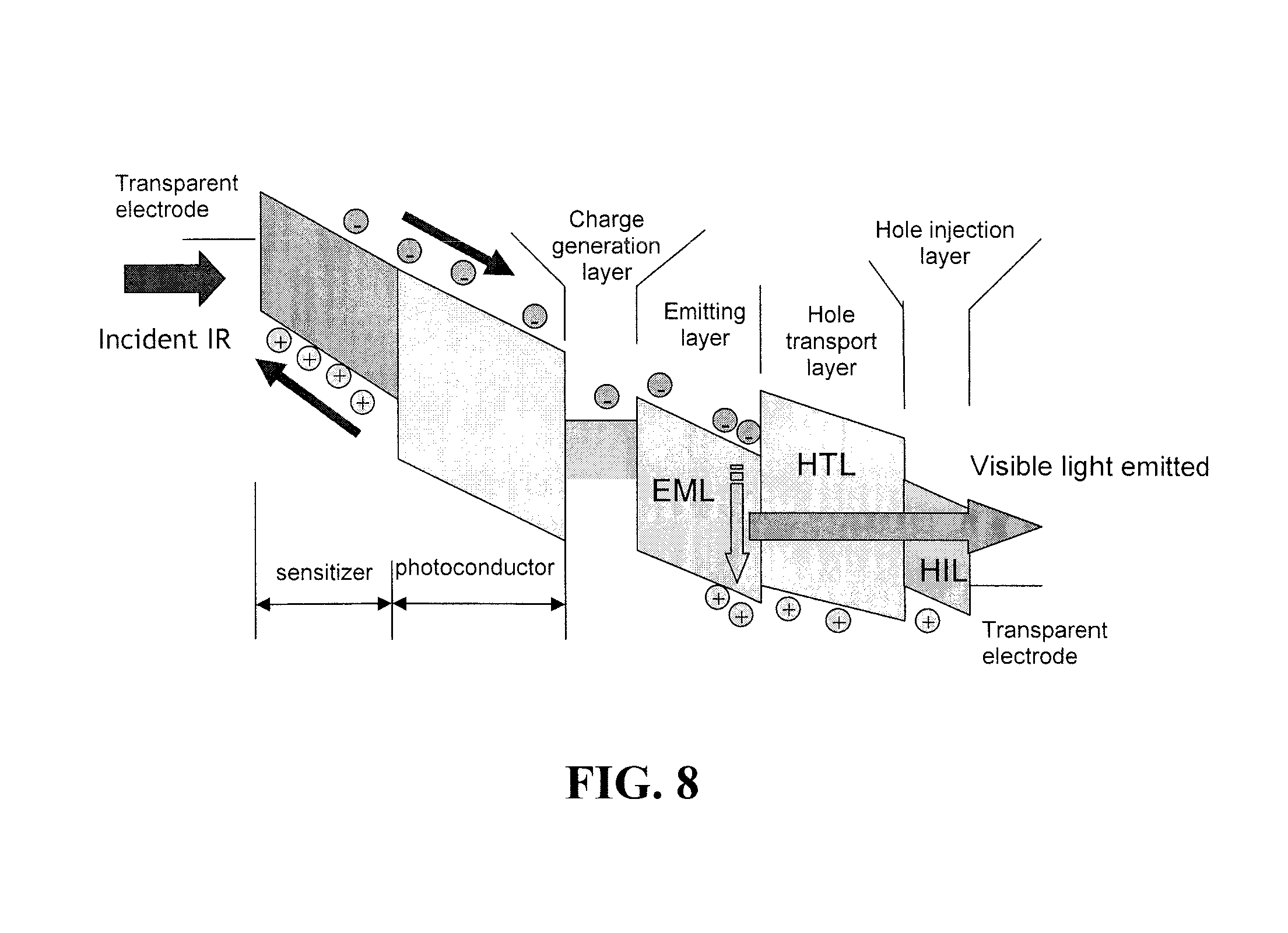
FIG. 8 shows an embodiment using a photoconductor as a light sensor.
DETAILED DESCRIPTION
Embodiments of the subject invention relate to a method and apparatus for infrared (IR) detection. A specific embodiment utilizes organic layers to produce a phototransistor for the detection of IR radiation. The wavelength range of the IR detector can be modified by incorporating materials sensitive to photons of different wavelengths. In a specific embodiment, quantum dots of materials sensitive to photons of different wavelengths than the host organic material of the absorbing layer of the phototransistor can be incorporated into the absorbing layer so as to enhance the absorption of photons having wavelengths associated with the material of the quantum dots.
In another embodiment, a photoconductor structure can be used instead of a phototransistor. In one embodiment, the photoconductor can incorporate PbSe or PbS quantum dots. In another embodiment, the photoconductor can incorporate organic materials.
Specific embodiments also involve displaying a detected IR image to a user. In a specific embodiment, organic materials can be used to create an organic light-emitting device. Additional material that emits at different wavelengths can be added to the light-emitting layer. In a specific embodiment, quantum dots of materials associated with emission of photons of different wavelengths than the host organic material of the emission layer can be incorporated into the emission layer to enhance the output display of the organic light-emitting device to the user. In a preferred embodiment, the IR detection is accomplished with a phototransistor and the displaying of the detected IR image is accomplished with an organic light-emitting device such as an organic light-emitting diode (OLED). In a more preferred embodiment, the phototransistor and OLED are in series.
Embodiments of the subject invention pertain to a method and apparatus for night vision. In an embodiment, a night vision device can be accomplished by the deposition of layers of organic thin films. Embodiments of the subject device can operate at low operating voltages, such as 10-15 V. In addition, the cost of manufacturing specific embodiments of the subject device can be lower than the cost of manufacturing conventional night vision systems. In an embodiment of the subject night vision device an organic phototransistor can be in series with an organic light-emitting device, such as an organic light-emitting diode (OLED).
Preferably, electrodes that are transparent to infrared light are used to allow IR radiation to enter the phototransistor. A schematic diagram of an embodiment of an IR sensor/detector, an embodiment of an IR sensor-display combination, and a circuit model for the IR sensor-display combination are shown in FIG. 1. A PNP bipolar phototransistor created using layers of organic material is shown on the left of FIG. 1. Here, CuPc is the n-layer and PTCBI is the p-layer. Although the curved arrow symbolizing light (absorbing IR and emitting green) are shown pointing to the absorption layer and emission layer, respectively, the IR light enters from the top and the visible light is emitted from the bottom of the device shown in FIG. 1. In the middle of FIG. 1, the integration of the phototransistor shown on the left with an OLED is shown. IR images can be incident on the top of the electrode layer (NiO) of the phototransistor and pass through the CuPc layer and into the absorption layer (PTCBI).
Upon photoexcitation with infrared light, charge carriers are generated in the phototransistor and injected into the OLED, which then generates photons in the visible range. Because of the low conductivity of organic thin films, the electric field will be confined within the photoexcited area and visible photons will be generated within the excited area. As a result, if a broad area device is exposed to an infrared image, a visible image will be generated. Preferably, an electrode transparent to visible light is used at the bottom, where the output image is emitted. In the embodiment shown, ITO is used as an electrode, which is transparent to visible light. Other materials can also be used. A circuit diagram of the integrated device shown in the middle is shown on the right side of FIG. 1. In a specific embodiment, no electronics are required to operate the device. In an embodiment, the operating voltages of the phototransistor and the light-emitting device are less than 10 V, such that the total operating voltages can be less than 20 V. This device can be made very light weight.
In an embodiment, glass can be used as a substrate for fabrication. The entire phototransistor and OLED combination can be very thin, for example, less than 1 .mu.m. The glass substrate with the thin layer can then be made part of night vision goggles where the thin layer is positioned to receive an IR image and a user is positioned to see the visible image emitted from the glass, or plastic, substrate.
FIG. 2 shows the PNP bipolar transistor of FIG. 1 and an NPN phototransistor, which can also be utilized in accordance with the subject invention.
The fabrication procedure for a specific embodiment of the subject IR detector-display combination will now be described. This fabrication procedure does not require any patterning. Other fabrication techniques, as well as other materials, as would be apparent to one skilled in the art having the benefit of the subject disclosure, can also be utilized in accordance with the subject invention. Devices are grown on a glass substrate or plastic substrate precoated with a 100 nm thick layer of indium-tin-oxide having a sheet resistance of 20 ohms/square. Substrates are degreased with solvents and then cleaned by exposure to oxygen plasma and UV-ozone ambient. All layers are vacuum deposited grown in succession without breaking the vacuum. In the first deposition step on top of the indium-tin-oxide (ITO) layer, to fabricate the integrated PNP phototransistor and OLED shown in the middle of FIG. 1, a 10-nm-thick CuPc is deposited as a hole injection layer. A 50 nm-thick NPD layer is then grown and acts as a hole transport layer. Next, a 60 nm-thick Alq3 emissive layer is deposited. A LiF(2 nm)/NiO (10 nm) charge generation layer is then deposited. This results in an OLED. To fabricate the phototransistor on the top of the light emitting device, a 40 nm thick CuPc layer, a 50 nm thick PTCBI layer, a 40 nm thick CuPc layer, and a 1000 nm NiO layer are then deposited.
In another specific embodiment, referring to FIG. 3, the PTCBI layer of the phototransistor is replaced with a PbS or PbSe quantum dot layer. The PbS or PbSe absorbs photons of different wavelengths than the PTCBI layer. As an example, a PTCBI layer can be created that absorbs photons up to wavelengths of about 1 .mu.m and a PbSe quantum dot layer, or PbS quantum dot layer, can be created that also absorbs photons having wavelengths in the range of about 1 .mu.m to about 3 .mu.m, so as to expand to wavelength range for detection. Other wavelength ranges can be accomplished by proper selection of the material in the absorption layer.
In a further specific embodiment, referring to FIG. 4, the 60 nm Alq3 layer of the light emitting device from FIG. 1 or FIG. 3 is replaced with a 50 nm Alq3 layer and a CdSe quantum dot layer. The material for the quantum dot layer can facilitate emission of light at wavelengths different from the light emitted by the Alq3 layer. Accordingly, other materials can also be utilized in accordance with the subject invention.
FIG. 5 shows structures of materials that can be utilized with embodiments of the subject invention. Shown in FIG. 5 are structures for tris-(8-hydroxyquinoline) aluminum (Alq3), 4-4'-bis[N-(1-naphthyl)-N-phenyl-amino]biphenyl (NPD), copper phthalocyanine (CuPc), and perylene-3,4!8,10-tetra-carboxylic-diimide-di.about.2,6-isopropy.about.ph- enyl (PTCDI).
Although exemplary embodiments directed to a phototransistor and phototransistor/OLED combination fabricated primarily from organic material layers have been described, additional embodiments can utilize inorganic materials for the phototransistor and/or the light emitting device. Examples of inorganic materials that can be used to fabricate phototransistors and/or light emitting device in accordance with the subject invention include, but are not limited to, amorphous silicon, germanium, and diamond-like carbon. Thin film amorphous silicon could have PbSe or PbS to absorb IR. An inorganic OLED can use ZnO to emit visible light. The use of inorganic materials in the absorption layer can allow detection of IR with wavelengths in the range of about 1 .mu.m to 4 .mu.m. These materials and the techniques to fabricate phototransistors and/or OLED's with structures similar to those shown in FIGS. 1, 2, 3, and 4 are known to those skilled in the art. In this way, an inorganic phototransistor can be incorporated with an organic OLED and an organic phototransistor can be incorporated with an inorganic OLED.
Embodiments of the present invention can incorporate a photoconductor. In specific embodiments, a photoconductor can replace the phototransistor described in the above embodiments. FIG. 6 shows a photoconductor device incorporating PbSe quantum dots. The PbSe quantum dots can be used to sense photons with wavelengths between 1 .mu.m to 3 .mu.m. The photoconductor structure can be formed of photoconductive material arranged between two electrodes. In one embodiment, one electrode can be formed of gold (Au) and the second electrode can be formed of ITO. In an embodiment, PbS quantum dots can be used in the place of the PbSe quantum dot layer. In operation, carriers can be photoexcited in the quantum dot (QD) layer through the absorption of IR rays. The carriers can travel to an OLED element to emit, for example, green light. In particular, electrons may be injected into an emissive layer of the OLED element and recombine with holes to give off light.
In the embodiment shown in FIG. 6, the photoconductor can be formed on an OLED element. The OLED element can be formed on a glass substrate and can incorporate an ITO layer formed on the substrate, a CuPc layer formed on the ITO layer to act as a hole transport layer, a NPD layer formed on the CuPc layer to act as a hole transport layer, an Alq layer formed on the NPD layer, and a LiF/NiO layer for charge generation formed on the Alq layer. The photoconductor can be formed on the LiF/NiO layer by depositing a gold layer on the LiF/NiO layer, forming a photoconductive material layer on the gold layer, and forming an ITO layer on the photoconductive material layer.
FIG. 7 shows a photoconductor device incorporating organic materials. Referring to FIG. 7, one of the electrodes for the photoconductor can be eliminated when incorporated with an OLED element. In particular, the photoconductive material can be in direct contact with a hole transporting layer of an OLED. In an embodiment, titanyl phthalocyanine (TiOPc) can be used as the photoconductive material of a photoconductor device. The TiOPc can respond to IR rays because TiOPc absorbs wavelengths at 0.8 .mu.m. The OLED element can be formed on a glass substrate and can include an ITO layer formed on the substrate, a LiF/NiO layer formed on the ITO layer, an Alq layer formed on the LiF/NiO layer and a NPD layer formed on the Alq Layer. The photoconductive material can be formed directly on the NPD layer without an intervening electrode.
FIG. 8 shows an embodiment incorporating a photoconductor as the light sensor. A photoconductor can have very large gain or amplification and is ideal to amplify the signal. The photoconductor device includes two layers, a charge transport layer and a sensitizer. NPD can be used as a charge transport layer and PbSe, PbS, and/or InAs quantum dots can be utilized for photon absorption.
In operation, carriers can be photoexcited in the TiOPc layer. The carriers can travel to the OLED element to emit, for example, green light. In particular, holes can be injected into the NPD layer to recombine with electrons and give off light.
In embodiments of the present invention, the gain in photoconductors can be as large as 100,000.
For embodiments incorporating photoconductors instead of phototransistors, fabrication may involve less process steps due to embodiments of photoconductors being single layer devices instead of a three-layer NPN or PNP structure.
All patents, patent applications, provisional applications, and publications referred to or cited herein are incorporated by reference in their entirety, including all figures and tables, to the extent they are not inconsistent with the explicit teachings of this specification.
It should be understood that the examples and embodiments described herein are for illustrative purposes only and that various modifications or changes in light thereof will be suggested to persons skilled in the art and are to be included within the spirit and purview of this application.
* * * * *
References
D00000
D00001
D00002
D00003
D00004
D00005
D00006
D00007
D00008
XML
uspto.report is an independent third-party trademark research tool that is not affiliated, endorsed, or sponsored by the United States Patent and Trademark Office (USPTO) or any other governmental organization. The information provided by uspto.report is based on publicly available data at the time of writing and is intended for informational purposes only.
While we strive to provide accurate and up-to-date information, we do not guarantee the accuracy, completeness, reliability, or suitability of the information displayed on this site. The use of this site is at your own risk. Any reliance you place on such information is therefore strictly at your own risk.
All official trademark data, including owner information, should be verified by visiting the official USPTO website at www.uspto.gov. This site is not intended to replace professional legal advice and should not be used as a substitute for consulting with a legal professional who is knowledgeable about trademark law.