Multi-level inverter
Yoscovich , et al.
U.S. patent number 10,680,505 [Application Number 16/442,161] was granted by the patent office on 2020-06-09 for multi-level inverter. This patent grant is currently assigned to Solaredge Technologies Ltd.. The grantee listed for this patent is Solaredge Technologies Ltd. Invention is credited to Yoav Galin, Tzachi Glovinsky, Guy Sella, Ilan Yoscovich.


View All Diagrams
| United States Patent | 10,680,505 |
| Yoscovich , et al. | June 9, 2020 |
Multi-level inverter
Abstract
A multi-level inverter having one or more banks, each bank containing a plurality of low voltage MOSFET transistors. A processor configured to switch the plurality of low voltage MOSFET transistors in each bank to switch at multiple times during each cycle.
| Inventors: | Yoscovich; Ilan (Ramat-Gan, IL), Glovinsky; Tzachi (Petah Tikva, IL), Sella; Guy (Raanana, IL), Galin; Yoav (Raanana, IL) | ||||||||||
|---|---|---|---|---|---|---|---|---|---|---|---|
| Applicant: |
|
||||||||||
| Assignee: | Solaredge Technologies Ltd.
(Herzeliya, IL) |
||||||||||
| Family ID: | 52727026 | ||||||||||
| Appl. No.: | 16/442,161 | ||||||||||
| Filed: | June 14, 2019 |
Prior Publication Data
| Document Identifier | Publication Date | |
|---|---|---|
| US 20190296633 A1 | Sep 26, 2019 | |
Related U.S. Patent Documents
| Application Number | Filing Date | Patent Number | Issue Date | ||
|---|---|---|---|---|---|
| 15054647 | Feb 26, 2016 | 10404154 | |||
| 14485682 | Apr 19, 2016 | 9318974 | |||
| 61970788 | Mar 26, 2014 | ||||
| Current U.S. Class: | 1/1 |
| Current CPC Class: | H02M 1/08 (20130101); H02M 7/537 (20130101); H02M 7/483 (20130101); H02M 1/143 (20130101); H02M 1/126 (20130101); H02M 2001/0054 (20130101); H02M 2007/4835 (20130101) |
| Current International Class: | H02M 1/08 (20060101); H02M 7/537 (20060101); H02M 1/14 (20060101); H02M 7/483 (20070101); H02M 1/12 (20060101); H02M 1/00 (20060101) |
References Cited [Referenced By]
U.S. Patent Documents
| 3581212 | May 1971 | McMurray |
| 3867643 | February 1975 | Baker et al. |
| 4270163 | May 1981 | Baker |
| 4336613 | June 1982 | Hewes |
| 4564895 | January 1986 | Glennon |
| 4670828 | June 1987 | Shekhawat et al. |
| 4816736 | March 1989 | Dougherty et al. |
| 4947100 | August 1990 | Dhyanchand et al. |
| 5172309 | December 1992 | DeDoncker et al. |
| 5233509 | August 1993 | Ghotbi |
| 5361196 | November 1994 | Tanamachi et al. |
| 5508658 | April 1996 | Nishioka et al. |
| 5598326 | January 1997 | Liu et al. |
| 5625539 | April 1997 | Nakata et al. |
| 5625545 | April 1997 | Hammond |
| 5638263 | June 1997 | Opal et al. |
| 5642275 | June 1997 | Peng et al. |
| 5644483 | July 1997 | Peng et al. |
| 5751138 | May 1998 | Venkata et al. |
| 5790396 | August 1998 | Miyazaki et al. |
| 5892677 | April 1999 | Chang |
| 5910892 | June 1999 | Lyons et al. |
| 5933339 | August 1999 | Duba et al. |
| 5936856 | August 1999 | Xiang |
| 5943229 | August 1999 | Sudhoff |
| 5982646 | November 1999 | Lyons et al. |
| 6005788 | December 1999 | Lipo et al. |
| 6031738 | February 2000 | Lipo et al. |
| 6058031 | May 2000 | Lyons et al. |
| 6060859 | May 2000 | Jonokuchi |
| 6075350 | June 2000 | Peng |
| 6160722 | December 2000 | Thommes et al. |
| 6205012 | March 2001 | Lear |
| RE37126 | April 2001 | Peng et al. |
| 6236580 | May 2001 | Aiello et al. |
| 6262555 | July 2001 | Hammond et al. |
| 6301130 | October 2001 | Aiello et al. |
| 6340851 | January 2002 | Rinaldi et al. |
| 6404655 | June 2002 | Welches |
| 6417644 | July 2002 | Hammond et al. |
| 6424207 | July 2002 | Johnson |
| 6459596 | October 2002 | Corzine |
| 6480403 | November 2002 | Bijlenga |
| 6519169 | February 2003 | Asplund et al. |
| 6556461 | April 2003 | Khersonsky et al. |
| 6577087 | June 2003 | Su |
| 6621719 | September 2003 | Steimer et al. |
| 6697271 | February 2004 | Corzine |
| 6757185 | June 2004 | Rojas Romero |
| 6850424 | February 2005 | Baudelot et al. |
| 6897784 | May 2005 | Goehlich |
| 6930899 | August 2005 | Bakran et al. |
| 6954366 | October 2005 | Lai et al. |
| 6969967 | November 2005 | Su |
| 7050311 | May 2006 | Lai et al. |
| 7190143 | March 2007 | Wei et al. |
| 7219673 | May 2007 | Lemak |
| 7230837 | June 2007 | Huang et al. |
| 7319763 | January 2008 | Bank et al. |
| 7372709 | May 2008 | Mazumder et al. |
| 7471532 | December 2008 | Salama et al. |
| 7495938 | February 2009 | Wu |
| 7499291 | March 2009 | Han |
| 7558087 | July 2009 | Meysenc et al. |
| 7573732 | August 2009 | Teichmann et al. |
| 7598714 | October 2009 | Stanley |
| 7663268 | February 2010 | Wen et al. |
| 7667342 | February 2010 | Matsumoto et al. |
| 7679941 | March 2010 | Raju et al. |
| 7710082 | May 2010 | Escobar Valderrama et al. |
| 7719864 | May 2010 | Kernahan et al. |
| 7768350 | August 2010 | Srinivasan et al. |
| 7787270 | August 2010 | NadimpalliRaju et al. |
| 7830681 | November 2010 | Abolhassani et al. |
| 7834579 | November 2010 | Nojima |
| 7839023 | November 2010 | Jacobson et al. |
| 7920393 | April 2011 | Bendre et al. |
| 7932693 | April 2011 | Lee et al. |
| 7940537 | May 2011 | Abolhassani et al. |
| 7969126 | June 2011 | Stanley |
| 7986535 | July 2011 | Jacobson et al. |
| 8018331 | September 2011 | Jang |
| 8026639 | September 2011 | Sachdeva et al. |
| 8031495 | October 2011 | Sachdeva et al. |
| 8045346 | October 2011 | Abolhassani et al. |
| 8144490 | March 2012 | El-Barbari et al. |
| 8144491 | March 2012 | Bendre et al. |
| 8169108 | May 2012 | Dupuis et al. |
| 8279640 | October 2012 | Abolhassani et al. |
| 8294306 | October 2012 | Kumar et al. |
| 8314602 | November 2012 | Hosini et al. |
| 8344551 | January 2013 | Nielsen |
| 8374009 | February 2013 | Feng et al. |
| 8385091 | February 2013 | Nielsen |
| 8400796 | March 2013 | Dofnas et al. |
| 8411474 | April 2013 | Roesner et al. |
| 8427010 | April 2013 | Bose et al. |
| 8471514 | June 2013 | Zargari et al. |
| 8471604 | June 2013 | Permuy et al. |
| 8482156 | July 2013 | Spanoche et al. |
| 8498137 | July 2013 | Joseph |
| 8547717 | October 2013 | Kshirsagar |
| 8559193 | October 2013 | Mazumder |
| 8570776 | October 2013 | Kolar et al. |
| 8587141 | November 2013 | Bjerknes et al. |
| 8599588 | December 2013 | Adest et al. |
| 8619446 | December 2013 | Liu et al. |
| 8664796 | March 2014 | Nielsen |
| 8670255 | March 2014 | Gong et al. |
| 8854019 | October 2014 | Levesque et al. |
| 2004/0022081 | February 2004 | Erickson et al. |
| 2004/0024937 | February 2004 | Duncan et al. |
| 2005/0017656 | January 2005 | Takahashi et al. |
| 2005/0127853 | June 2005 | Su |
| 2005/0139259 | June 2005 | Steigerwald et al. |
| 2005/0141248 | June 2005 | Mazumder et al. |
| 2006/0044857 | March 2006 | Lemak |
| 2006/0197112 | September 2006 | Uchihara et al. |
| 2007/0296383 | December 2007 | Xu et al. |
| 2009/0196764 | August 2009 | Fogarty et al. |
| 2010/0060235 | March 2010 | Dommaschk et al. |
| 2010/0266875 | October 2010 | Somogye et al. |
| 2011/0013438 | January 2011 | Frisch et al. |
| 2011/0061705 | March 2011 | Croft et al. |
| 2011/0065161 | March 2011 | Kwasinski et al. |
| 2011/0280052 | November 2011 | Al-Haddad |
| 2012/0068555 | March 2012 | Aiello et al. |
| 2012/0106210 | May 2012 | Xu et al. |
| 2012/0112545 | May 2012 | Aiello et al. |
| 2012/0161858 | June 2012 | Permuy et al. |
| 2012/0163057 | June 2012 | Permuy et al. |
| 2012/0200163 | August 2012 | Ito et al. |
| 2012/0217943 | August 2012 | Haddad |
| 2012/0218785 | August 2012 | Li et al. |
| 2012/0218795 | August 2012 | Mihalache |
| 2012/0223583 | September 2012 | Cooley et al. |
| 2013/0002215 | January 2013 | Ikeda et al. |
| 2013/0014384 | January 2013 | Xue et al. |
| 2013/0033907 | February 2013 | Zhou et al. |
| 2013/0044527 | February 2013 | Vracar et al. |
| 2013/0051094 | February 2013 | Bendre et al. |
| 2013/0128629 | May 2013 | Clare et al. |
| 2013/0128636 | May 2013 | Trainer et al. |
| 2013/0154716 | June 2013 | Degener |
| 2013/0188406 | July 2013 | Pouliquen et al. |
| 2013/0208514 | August 2013 | Trainer et al. |
| 2013/0208521 | August 2013 | Trainer et al. |
| 2013/0221678 | August 2013 | Zhang et al. |
| 2013/0223651 | August 2013 | Hoyerby |
| 2013/0235626 | September 2013 | Jang et al. |
| 2013/0249322 | September 2013 | Zhang et al. |
| 2013/0264876 | October 2013 | Paakkinen |
| 2013/0272045 | October 2013 | Soeiro et al. |
| 2013/0279211 | October 2013 | Green et al. |
| 2013/0314957 | November 2013 | Gupta et al. |
| 2013/0322142 | December 2013 | Raju |
| 2014/0003101 | January 2014 | Tang et al. |
| 2014/0022738 | January 2014 | Hiller et al. |
| 2014/0046500 | February 2014 | Varma |
| 2014/0049230 | February 2014 | Weyh |
| 2014/0097808 | April 2014 | Clark et al. |
| 2014/0118158 | May 2014 | Parra et al. |
| 2014/0125241 | May 2014 | Elferich et al. |
| 2014/0167715 | June 2014 | Wu et al. |
| 2014/0198542 | July 2014 | Swamy |
| 2014/0198547 | July 2014 | Heo et al. |
| 2014/0198548 | July 2014 | Zhang |
| 2014/0232364 | August 2014 | Thomas |
| 2014/0293667 | October 2014 | Schroeder |
| 2014/0300413 | October 2014 | Hoyerby et al. |
| 2015/0009734 | January 2015 | Stahl et al. |
| 2015/0280608 | October 2015 | Yoscovich et al. |
| 2017/0310242 | October 2017 | Kifuji |
| 1625037 | Jun 2005 | CN | |||
| 101291129 | Oct 2008 | CN | |||
| 100431253 | Nov 2008 | CN | |||
| 101527504 | Sep 2009 | CN | |||
| 101546964 | Sep 2009 | CN | |||
| 101692579 | Apr 2010 | CN | |||
| 101795057 | Aug 2010 | CN | |||
| 101902143 | Dec 2010 | CN | |||
| 101917016 | Dec 2010 | CN | |||
| 101944839 | Jan 2011 | CN | |||
| 102013691 | Apr 2011 | CN | |||
| 102223099 | Oct 2011 | CN | |||
| 102355152 | Feb 2012 | CN | |||
| 102511121 | Jun 2012 | CN | |||
| 102545681 | Jul 2012 | CN | |||
| 102594192 | Jul 2012 | CN | |||
| 202333835 | Jul 2012 | CN | |||
| 102629836 | Aug 2012 | CN | |||
| 102651612 | Aug 2012 | CN | |||
| 102664514 | Sep 2012 | CN | |||
| 102684204 | Sep 2012 | CN | |||
| 202444420 | Sep 2012 | CN | |||
| 102709941 | Oct 2012 | CN | |||
| 102723734 | Oct 2012 | CN | |||
| 102739080 | Oct 2012 | CN | |||
| 102763316 | Oct 2012 | CN | |||
| 102868290 | Jan 2013 | CN | |||
| 102891602 | Jan 2013 | CN | |||
| 102959843 | Mar 2013 | CN | |||
| 102983002 | Mar 2013 | CN | |||
| 103001519 | Mar 2013 | CN | |||
| 202798507 | Mar 2013 | CN | |||
| 103066573 | Apr 2013 | CN | |||
| 103066878 | Apr 2013 | CN | |||
| 103107720 | May 2013 | CN | |||
| 103116665 | May 2013 | CN | |||
| 103123664 | May 2013 | CN | |||
| 103176470 | Jun 2013 | CN | |||
| 202997660 | Jun 2013 | CN | |||
| 103199681 | Jul 2013 | CN | |||
| 103208929 | Jul 2013 | CN | |||
| 103219738 | Jul 2013 | CN | |||
| 103219896 | Jul 2013 | CN | |||
| 103236800 | Aug 2013 | CN | |||
| 103248112 | Aug 2013 | CN | |||
| 103311947 | Sep 2013 | CN | |||
| 103312209 | Sep 2013 | CN | |||
| 103312246 | Sep 2013 | CN | |||
| 103441512 | Dec 2013 | CN | |||
| 103457501 | Dec 2013 | CN | |||
| 103518300 | Jan 2014 | CN | |||
| 203398807 | Jan 2014 | CN | |||
| 203399000 | Jan 2014 | CN | |||
| 103595284 | Feb 2014 | CN | |||
| 103607107 | Feb 2014 | CN | |||
| 103633870 | Mar 2014 | CN | |||
| 103701145 | Apr 2014 | CN | |||
| 103701350 | Apr 2014 | CN | |||
| 103731035 | Apr 2014 | CN | |||
| 103762873 | Apr 2014 | CN | |||
| 103762881 | Apr 2014 | CN | |||
| 10103031 | Jul 2002 | DE | |||
| 112010002784 | Aug 2012 | DE | |||
| 102012202173 | Aug 2013 | DE | |||
| 102012202187 | Aug 2013 | DE | |||
| 102012005974 | Sep 2013 | DE | |||
| 0010811 | May 1980 | EP | |||
| 0913918 | May 1999 | EP | |||
| 1113570 | Jul 2001 | EP | |||
| 1420976 | May 2004 | EP | |||
| 1657809 | May 2006 | EP | |||
| 1713168 | Oct 2006 | EP | |||
| 1051799 | Jul 2008 | EP | |||
| 2110939 | Oct 2009 | EP | |||
| 2160828 | Mar 2010 | EP | |||
| 2178200 | Apr 2010 | EP | |||
| 2256579 | Dec 2010 | EP | |||
| 2312739 | Apr 2011 | EP | |||
| 2372893 | Oct 2011 | EP | |||
| 2408081 | Jan 2012 | EP | |||
| 2495858 | Sep 2012 | EP | |||
| 2533412 | Dec 2012 | EP | |||
| 2560276 | Feb 2013 | EP | |||
| 2568589 | Mar 2013 | EP | |||
| 2568591 | Mar 2013 | EP | |||
| 2590312 | May 2013 | EP | |||
| 2596980 | May 2013 | EP | |||
| 2621076 | Jul 2013 | EP | |||
| 2650999 | Oct 2013 | EP | |||
| 2654201 | Oct 2013 | EP | |||
| 2677653 | Dec 2013 | EP | |||
| 2779410 | Sep 2014 | EP | |||
| 2882084 | Jul 2015 | EP | |||
| 2651024 | May 2017 | EP | |||
| 2010-220364 | Sep 2010 | JP | |||
| 2011-072118 | Apr 2011 | JP | |||
| 2011-130517 | Jun 2011 | JP | |||
| 2012-060735 | Mar 2012 | JP | |||
| 2012-065428 | Mar 2012 | JP | |||
| 2012-257451 | Dec 2012 | JP | |||
| 2013-055830 | Mar 2013 | JP | |||
| 2013-526247 | Jun 2013 | JP | |||
| 2013-258790 | Dec 2013 | JP | |||
| 2014-003821 | Jan 2014 | JP | |||
| 2014-050135 | Mar 2014 | JP | |||
| 0213364 | Feb 2002 | WO | |||
| 2006027744 | Mar 2006 | WO | |||
| 2009012008 | Jan 2009 | WO | |||
| 2010051645 | May 2010 | WO | |||
| 2011-093269 | Aug 2011 | WO | |||
| 2011114816 | Sep 2011 | WO | |||
| 2012010053 | Jan 2012 | WO | |||
| 2012010054 | Jan 2012 | WO | |||
| 2012024984 | Mar 2012 | WO | |||
| 2012099176 | Jul 2012 | WO | |||
| 2012118654 | Sep 2012 | WO | |||
| 2012126160 | Sep 2012 | WO | |||
| 2012140008 | Oct 2012 | WO | |||
| 2012144662 | Oct 2012 | WO | |||
| 2013005498 | Jan 2013 | WO | |||
| 2013017353 | Feb 2013 | WO | |||
| 2013086445 | Jun 2013 | WO | |||
| 2013089425 | Jun 2013 | WO | |||
| 2013091675 | Jun 2013 | WO | |||
| 2013110371 | Aug 2013 | WO | |||
| 2013120664 | Aug 2013 | WO | |||
| 2013126660 | Aug 2013 | WO | |||
| 2013136377 | Sep 2013 | WO | |||
| 2013137749 | Sep 2013 | WO | |||
| 2013143037 | Oct 2013 | WO | |||
| 2013167189 | Nov 2013 | WO | |||
| 2013177303 | Nov 2013 | WO | |||
| 2013185825 | Dec 2013 | WO | |||
| 2014004065 | Jan 2014 | WO | |||
| 2014006200 | Jan 2014 | WO | |||
| 2014007432 | Jan 2014 | WO | |||
| 2014024185 | Feb 2014 | WO | |||
| 2014030202 | Feb 2014 | WO | |||
| 2014042118 | Mar 2014 | WO | |||
| 2014047733 | Apr 2014 | WO | |||
| 2014082221 | Jun 2014 | WO | |||
| 2014082655 | Jun 2014 | WO | |||
| 2014082657 | Jun 2014 | WO | |||
| 2014104839 | Jul 2014 | WO | |||
| 2015120023 | Aug 2015 | WO | |||
Other References
|
Alonso, et al., "Cascaded H-Bridge Multilevel Converter for Grid Connected Photovoltaic Generators with Independent Maximum Power Point Tracking of Each Solar Array", 2003 IEEE 34th, Annual Power Electronics Specialists Conference, Acapulco, Mexico, Jun. 15-19, 2003, pp. 731-735, vol. 2. cited by applicant . Walker, "Cascaded DC-DC Converter Connection of Photovoltaic Modules", 33rd Annual IEEE Power Electronics Specialists Conference. PESC 2002. Conference Proceedings. Cairns, Queensland, Australia, Jun. 23-27, 2002; [Annual Power Electronics Specialists Conference], New York, NY: IEEE US, vol. 1, Jun. 23, 2002, pp. 24-29, XP010596060 ISBN: 978-0-7803-7262-7, figure 1. cited by applicant . Duarte, "A Family of ZVX-PWM Active-Clamping DC-to-DC Converters: Synthesis, Analysis and Experimentation", Telecommunications Energy Conference, 1995, INTELEC '95, 17th International The Hague, Netherlands, Oct. 29-Nov. 1, 1995, New York, NY, US, IEEE, US, Oct. 29, 1995, pp. 502-509, XP010161283 ISBN: 978-0-7803-2750-4 p. 503-504. cited by applicant . Iyomori H et al: "Three-phase bridge power block module type auxiliary resonant AC link snubber-assisted soft switching inverter for distributed AC power supply", INTELEC 2003. 25th. International Telecommunications Energy Conference. Yokohama, Japan, Oct. 19-23, 2003; Tokyo, IEICE, JP, Oct. 23, 2003 (Oct. 23, 2003), pp. 650-656, XP031895550, ISBN: 978-4-88552-196-6. cited by applicant . Yuqing Tang: "High Power Inverter EMI characterization and Improvement Using Auxiliary Resonant Snubber Inverter", Dec. 17, 1998 (Dec. 17, 1998), XP055055241, Blacksburg, Virginia Retrieved from the Internet: URL:http:jscholar.lib.vt.edu/theses/available/etd-012299-165108/unrestric- ted/THESIS. PDF, [retrieved on Mar. 5, 2013]. cited by applicant . Yoshida M et al: "Actual efficiency and electromagnetic noises evaluations of a single inductor resonant AC link snubber-assisted three-phase soft-switching inverter", INTELEC 2003. 25th. International Telecommunications Energy Conference. Yokohama, Japan, Oct. 19-23, 2003; Tokyo, IEICE, JP, Oct. 23, 2003 (Oct. 23, 2003), pp. 721-726, XP031895560, ISBN: 978-4-88552-196-6. cited by applicant . Third party observation--EP07874025.5--Mailing date: Aug. 6, 2011. cited by applicant . Meynard, T. A., and Henry Foch. "Multi-level conversion: high voltage choppers and voltage-source inverters." Power Electronics Specialists Conference, 1992. PESC'92 Record., 23rd Annual IEEE. IEEE, 1992. cited by applicant . Gow Ja A et al: "A Modular DC-DC Converter and Maximum Power Tracking Controller Formedium to Large Scale Photovoltaic Generating Plant"8<SUP>th </SUP> European Conference on Power Electronics and Applications. Lausaane, CH, Sep. 7-9, 1999, EPE. European Conference on Power Electronics and Applications, Brussls: EPE Association, BE, vol. Conf. 8, Sep. 7, 1999, pp. 1-8, XP000883026. cited by applicant . Matsuo H et al: "Novel Solar Cell Power Supply System Using the Miltiple-input DC-DC Converter" 20<SUP>th</SUP> International telecommunications Energy Conference. Intelec '98 San Francisco, CA, Oct. 4-8, 1998, Intelec International Telecommunications Energy Conference, New York, NY: IEEE, US, Oct. 4, 1998, pp. 797-802, XP000896384. cited by applicant . Xiaofeng Sun, Weiyang Wu, Xin Li, Qinglin Zhao: A Research on Photovoltaic Energy Controlling System with Maximum Power Point Tracking:; Proceedings of the Power Conversion Conference--Osaka 2002 (Cat. No. 02TH8579) IEEE--Piscataway, NJ, USA, ISBN 0-7803-7156-9, vol. 2, p. 822-826, XP010590259: the whole document. cited by applicant . Meinhardt, Mike, et al., "Multi-String-Converter with Reduced Specific Costs and Enhanced Functionality," Solar Energy, May 21, 2001, pp. 217-227, vol. 69, Elsevier Science Ltd. cited by applicant . Martins, et al.: "Interconnection of a Photovoltaic Panels Array to a Single-Phase Utility Line From a Static Conversion System"; Power Electronics Specialists Conference, 2000. PESC 00. 2000 IEEE 31st Annual; Jun. 18, 2000-Jun. 23, 2000; ISSN: 0275-9306; pp. 1207-1211, vol. 3. cited by applicant . Shimizu, Toshihisa, et al., "A Flyback-type Single Phase Utility Interactive Inverter with Low-frequency Ripple Current Reduction on the DC Input for an AC Photovoltaic Module System," IEEE 33rd Annual Power Electronics Specialist Conference, Month Unknown, 2002, pp. 1483-1488, vol. 3, IEEE. cited by applicant . Zhang et al., "Capacitor voltage balancing in multilevel flying capacitor inverters by rule-based switching pattern selection", May 2007, p. 339-347. cited by applicant . Partial European Search Report--EP Appl. 14159869--dated Sep. 14, 2015. cited by applicant . Liu et al. "A Compact Power Converter for High Current and Low Voltage Applications", Industrial Electronics Society, 39th Annual Conference of the IEE, Nov. 2013, p. 140-144. cited by applicant . European Search Report--EP Appl. 15160896.5--dated Oct. 23, 2015. cited by applicant . European Extended Search Report--EP Appl. 14159869.8--dated Jan. 12, 2016. cited by applicant . Su, Gui-Jia: "Multilevel DC-Link Inverter", IEEE Transactions on Industry Applications, IEEE Service Center, Piscataway, NJ, US, vol. 41, No. 3, May 2, 2005, pp. 848-854, XP11132530. cited by applicant . Jun. 26, 2017--Chinese Office Action--CN 201410094169.8. cited by applicant . 2008--"Simulink Model of Flying Capacitor Multilevel Inverter"--Adrian Schiop, et al.--11th International Conference on Optimization of Electrical and Electronic Equipment. cited by applicant . Jul. 14, 2017--Chinese Office Action--CN 201510133812.8. cited by applicant . Feb. 13, 2017--EP Search Report EP App 17203127. cited by applicant . 2012--Konstantinou et al., "The Seven-level Flying Capacitor based ANPC Converter for Grid Intergration of Utility-Scale PV Systems" 3rd IEEE International Symposium on Power Electronics for Distributed Generation Systems (PEDG) p. 592-597. cited by applicant . Oct. 2012--Pulikanti et. al, "DC-Link Voltage Ripple Compensation for Multilevel Active-Neutral-Point-Clamped Converters Operated with SHE-PWM" IEEE Transactions on Power Deliver, vol. 27, No. 4 p. 2176-2184. cited by applicant . 2008--Winkelnkemper et. al, "Control of a 6MVA Hybrid Converter for a Permanent Magnet Synchronous Generator for Windpower" Proceedings of the 2008 International Conference on Electrical Machines p. 2-6. cited by applicant . Dec. 5-8, 2011--Muneshima et. al, "A New Time-Sharing Charge 5L Inverter" IEEE PEDS 2011 p. 115-120. cited by applicant . Sep. 20-24, 2009--Li et. al, "An Optimum PWM Strategy for 5-Level Active NPC (ANPC) Converter Based on Real-time Solution for THD Minimization" p. 1976-1982. cited by applicant . Mar. 14-17, 2010--Kiefemdortt, et. al, "A New Medium Voltage Drive System Based on ANPC-5L Technology" p. 643-649. cited by applicant . 2012--Pulikanti et. al, "Generalisation of flying capacitor-based active-neutral-point-clamped multilevel converter using voltage-level modulation" IET Power Electron, 2012, vol. 5, Issue 4, p. 456-466. cited by applicant . Sep. 15-19, 2013--Wang et. al, "Capacitor Voltage Balancing of Five-Level ANPC Converter based on Zero-Sequence Voltage Injection Using PS-PWM" p. 4035-4040. cited by applicant . Sep. 13, 2013--Notice of Opposition, EP App No. 15160896.5. cited by applicant . Mar. 26, 2014--Yoscovich, et al. "Multi-level Inverter" U.S. Appl. No. 61/970,788. cited by applicant . Sep. 13, 2014--Yoscovich, et al., "Multi-level Inverter" U.S. Appl. No. 14/485,6825. cited by applicant . Boller, Optimale Ansteuerung von Mittelspannungswechselrichtern, Diss Uni Wuppertal, Nov. 11, 2011. cited by applicant . Choi, Capacitor Voltage Balancing of Flying Capacitor Multilevel Converters by Space Vector PWM, Jul. 2012. cited by applicant . Cramer, Modulorientierter Stromrichter Geht In Serienfertigung , SPVSE, 1994. cited by applicant . Cramer, String-Wechselrichter Machen Solarstrom Billiger, Elektronik, Sep. 1996. cited by applicant . Engler, Begleitende Untersuchungen zur Entwicklung eines Multi-String-Wechselrichters, SPVSE, Mar. 2002. cited by applicant . Feng, A Novel Voltage Balancing Control Method for Flying Capacitor Multilevel Converters, IEEE, 2003. cited by applicant . Feng, Modified phase-shifted PWM control for flying capacitor multilevel converters. IEEE Transactions on Power Electronics, 2007. cited by applicant . Fishelov, Immer Maximale Leistung, Elektronik, 2010. cited by applicant . Geipel, Untersuchungen zur Entwicklung modulorientierter Stromrichter for netzgekoppelte Photovoltaik-Anlagen, SPVSE, 1995. cited by applicant . Ghias, Voltage Balancing Method for the Multilevel Flying Capacitor Converter Using Phase-Shifted PWM, Dec. 2012. cited by applicant . Hu, Active Power Filtering by a Flying-Capacitor Multilevel Inverter with Capacitor Voltage Balance, IEEE, 2008. cited by applicant . Kang, A Symmetric Carrier Technique of CRPWM for Voltage Balance Method of Flying-Capacitor Multilevel Inverter, Jun. 2005. cited by applicant . Khazraei, A Generalized Capacitor Voltage Balancing Scheme for Flying Capacitor Multilevel Converters, IEEE, 2010. cited by applicant . Khazraei, Active Capacitor Voltage Balancing in Single-Phase Flying-Capacitor Multilevel Power Converters, IEEE, Feb. 2012. cited by applicant . Mcgrath, Analytical Modelling of Voltage Balance Dynamics for a Flying Capacitor Multilevel Converter, 2007. cited by applicant . Niebauer, Solarenergie Optimal Nutzen, Elektronik, 1996. cited by applicant . Schettler, Selbst Gefuhrte pulswechselrichtemit Gleichspannungskreis Fur den Einsatz in Hochspannungsnetzen zur Sicherung der Energiequoitlat mittals Wirk-und Blindleistun, Pulswechselrichter, VDI, 2004. cited by applicant . Shukla, Improved Multilevel Hysteresis Current Regulation and Capacitor Voltage Balancing Schemes for Flying Capacitor Multilevel Inverter, IEEE, Mar. 2008. cited by applicant . Zhang, Three-phase four-leg flying-capacitor multi-level inverter-based active power filter for unbalanced current operation, 2013. cited by applicant . Wang et al, Self-precharge of floating capacitors in a five-level ANPC inverter, Proceedings of The 7th International Power Electronics and Motion Control Conference, 1776-1780, Jun. 2012. cited by applicant . Janik et al, Universal precharging method for de-link and flying capacitors of four-level Flying Capacitor Converter, 6322-6327, 2013. cited by applicant . Mar. 5, 2020--CN Office Action--CN 201811175971.4. cited by applicant. |
Primary Examiner: Laxton; Gary L
Assistant Examiner: Jackson; Lakaisha
Attorney, Agent or Firm: Banner & Witcoff, Ltd.
Parent Case Text
RELATED APPLICATIONS
The present application is a continuation of U.S. Non-Provisional application Ser. No. 15/054,647, entitled "MULTI-LEVEL INVERTER WITH FLYING CAPACITOR TOPOLOGY", filed Feb. 26, 2016, which is a continuation of U.S. Non-Provisional application Ser. No. 14/485,682, entitled "MULTI-LEVEL INVERTER" filed Sep. 13, 2014, which claims priority to U.S. Provisional Application No. 61/970,788, entitled "MULTI-LEVEL INVERTER" filed on Mar. 26, 2014. These applications are hereby incorporated by reference in their entirety. The present application is related to U.S. patent application Ser. No. 13/826,556, entitled "MULTI-LEVEL INVERTER," filed Mar. 14, 2013, which is hereby incorporated by reference in its entirety.
Claims
We claim:
1. An inverter comprising: first and second DC terminals configured to receive a DC voltage; first and second AC terminals configured to output an AC voltage at a first frequency; a first flying capacitor circuit comprising first and second voltage inputs, and a first voltage output coupled to the first AC terminal; a second flying capacitor circuit comprising third and fourth voltage inputs, and a second voltage output coupled to the second AC terminal; and a switching circuit having a first plurality of switches configured to operate at the first frequency and a second plurality of switches configured to operate at the first frequency; wherein: during a first half cycle of the AC voltage, the first plurality of switches is configured to connect the first DC terminal to the first voltage input, the second DC terminal to the fourth voltage input, and the second voltage input to the third voltage input; and during a second half cycle of the AC voltage, the second plurality of switches is configured to connect the first DC terminal to the third voltage input, the second DC terminal to the second voltage input, and the fourth voltage input to the first voltage input.
2. The inverter of claim 1, wherein the switching circuit is configured to switch the first plurality of switches substantially complimentary to switching the second plurality of switches at the first frequency.
3. The inverter of claim 2, wherein the first plurality of switches is configured to connect and disconnect the second voltage input to the third voltage input with mutual dead time to the second plurality of switches being configured to connect and disconnect the fourth voltage input to the first voltage input.
4. The inverter of claim 1, wherein: the second plurality of switches comprises a first switch connected between an intersection point and the first voltage input, and a fourth switch connected between the intersection point and the fourth voltage input; and the first plurality of switches comprises a second switch connected between the intersection point and the second voltage input, and a third switch connected between the intersection point and the third voltage input.
5. The inverter of claim 1, wherein: the first plurality of switches comprises at least one first switch connected between the second voltage input and the third voltage input; and the second plurality of switches comprises at least one second switch connected between the fourth voltage input and the first voltage input.
6. The inverter of claim 1, wherein: the first plurality of switches and the second plurality of switches comprise a first switch connected between the first DC terminal and the first voltage input, a second switch connected between the second DC terminal and the second voltage input, a third switch connected between the first DC terminal and the third voltage input, and a fourth switch connected between the second DC terminal and the fourth voltage input; and the inverter further comprises a controller configured to control the first switch and the fourth switch to be on during the first half cycle and to be off during the second half cycle, and the second switch and the third switch to be off during the first half cycle and to be on during the second half cycle.
7. The inverter of claim 1, further comprising: a first inductor connected between the first voltage output and the first AC terminal; and a second inductor connected between the second voltage output and the second AC terminal.
8. The inverter of claim 7, wherein: the inverter is configured to generate a first sine wave voltage on the first AC terminal and a second sine wave voltage on the second AC terminal; the first sine wave voltage is 180 degrees phase shifted from the second sine wave voltage; and the AC voltage is output as a difference between the first and the second sine wave voltages.
9. The inverter of claim 1, wherein the first plurality of switches and the second plurality of switches are configured to share current between the first flying capacitor circuit and the second flying capacitor circuit such that ripple voltage is removed across the first and the second voltage inputs and removed across the third and the fourth voltage inputs.
10. The inverter of claim 9, wherein: the first flying capacitor circuit comprises a third plurality of switches, the second flying capacitor circuit comprises a fourth plurality of switches, and the third plurality of switches and the fourth plurality of switches are configured to switch at a second frequency that is greater than the first frequency; and a first connection made by the first plurality of switches between the second and the third voltage inputs, and a second connection made by the second plurality of switches between the fourth and the first voltage inputs are configured to filter current at the second frequency from flowing between the first and the second flying capacitor circuits.
11. The inverter of claim 1, further comprising a controller, wherein: the first flying capacitor circuit comprises a third plurality of switches, the second flying capacitor circuit comprises a fourth plurality of switches, and the third plurality of switches corresponds one-to-one with the fourth plurality of switches; and the controller is configured to switch the third plurality of switches and the fourth plurality of switches at a second frequency that is greater than the first frequency such that, during each cycle of the second frequency, each switch of the third plurality of switches turns on and off in a complementary manner to its corresponding switch of the fourth plurality of switches.
12. The inverter of claim 1, further comprising a controller, wherein: the first flying capacitor circuit comprises a third plurality of switches, and the second flying capacitor circuit comprises a fourth plurality of switches; and during the first and the second half cycles of the AC voltage, the controller is configured to switch the third plurality of switches and the fourth plurality of switches at a second frequency that is greater than the first frequency and that is greater than 16 kHz.
13. The inverter of claim 12, wherein the first frequency is 50 Hz or 60 Hz.
14. A method comprising: generating an AC voltage at a first frequency with an inverter comprising first and second DC terminals, first and second AC terminals, a switching circuit having a first plurality of switches and a second plurality of switches, a first flying capacitor circuit having first and second voltage inputs and a first voltage output coupled to the first AC terminal, and a second flying capacitor circuit having third and fourth voltage inputs and a second voltage output coupled to the second AC terminal; wherein the generating comprises: receiving a DC voltage across the first and the second DC terminals; and switching the first plurality of switches and the second plurality of switches at the first frequency, including: a) closing, during first half cycles of the AC voltage, the first plurality of switches to connect the first DC terminal to the first voltage input, the second DC terminal to the fourth voltage input, and the second voltage input to the third voltage input; and b) closing, during second half cycles of the AC voltage, the second plurality of switches to connect the first DC terminal to the third voltage input, the second DC terminal to the second voltage input, and the fourth voltage input to the first voltage input.
15. The method of claim 14, further comprising switching the first plurality of switches substantially complimentary to switching the second plurality of switches at the first frequency.
16. The method of claim 15, wherein the switching of the first plurality of switches substantially complimentary to the switching of the second plurality of switches at the first frequency comprises connecting and disconnecting the second voltage input to the third voltage input with mutual dead time to connecting and disconnecting of the fourth voltage input to the first voltage input.
17. The method of claim 14, wherein: the second plurality of switches comprise a first switch connected between an intersection point and the first voltage input, and a fourth switch connected between the intersection point and the fourth voltage input; and the first plurality of switches comprise a second switch connected between the intersection point and the second voltage input, and a third switch connected between the intersection point and the third voltage input.
18. The method of claim 14, wherein: the first plurality of switches comprises at least one first switch connected between the second voltage input and the third voltage input; and the second plurality of switches comprises at least one second switch connected serially between the fourth voltage input and the first voltage input.
19. The method of claim 14, further comprising: generating, with the first flying capacitor circuit, a first pulse width modulated voltage on the first voltage output; generating, with the second flying capacitor circuit, a second pulse width modulated voltage on the second voltage output; filtering the first pulse width modulated voltage to generate a first sine wave voltage at the first frequency on the first AC terminal; filtering the second pulse width modulated voltage to generate a second sine wave voltage at the first frequency on the second AC terminal; wherein the first sine wave voltage is 180 degrees phase shifted from the second sine wave voltage.
20. The method of claim 14, further comprising conducting current from the second voltage input to the third voltage input during the first half cycles, and current from the fourth voltage input to the first voltage input during the second half cycles, such that ripple voltage at the first frequency is removed across the first and the second voltage inputs, and removed across the third and the fourth voltage inputs.
21. The method of claim 20, further comprising: switching, at a second frequency that is greater than the first frequency, a third plurality of switches in the first flying capacitor circuit and a fourth plurality of switches in the second flying capacitor circuit; and filtering current at the second frequency from flowing between the first flying capacitor circuit and the second flying capacitor circuit.
22. The method of claim 14, wherein the first flying capacitor circuit comprises a third plurality of switches, the second flying capacitor circuit comprises a fourth plurality of switches, the third plurality of switches correspond one-to-one with the fourth plurality of switches, and the method further comprises: switching each switch of the third plurality of switches in a complementary manner to its corresponding switch in the fourth plurality of switches.
23. The method of claim 14, wherein the first flying capacitor circuit comprises a third plurality of switches and the second flying capacitor circuit comprises a fourth plurality of switches, and the method further comprises: switching on and off the third plurality of switches and the fourth plurality of switches at a second frequency that is greater than the first frequency and that is greater than 16 kHz.
24. The method of claim 23, wherein the first frequency is 50 Hz or 60 Hz.
25. An inverter comprising: first and second DC terminals configured to receive a DC voltage; first and second AC terminals configured to output an AC voltage at a first frequency; a first flying capacitor circuit comprising first and second voltage inputs, and a first voltage output coupled to the first AC terminal; a second flying capacitor circuit comprising third and fourth voltage inputs, and a second voltage output coupled to the second AC terminal; a first plurality of switches configured to switch at the first frequency, including closing during first half cycles of the AC voltage to connect the first DC terminal to the first voltage input, the second DC terminal to the fourth voltage input, and the second voltage input to the third voltage input; and a second plurality of switches configured to switch at the first frequency, including closing during second half cycles of the AC voltage to connect the first DC terminal to the third voltage input, the second DC terminal to the second voltage input, and the fourth voltage input to the first voltage input; wherein, during outputting of the AC voltage: the first plurality of switches is configured to open whenever the first DC terminal is connected to the third voltage input, and the second plurality of switches is configured to open whenever the first DC terminal is connected to the first voltage input.
26. The inverter of claim 25, wherein: the first flying capacitor circuit comprises a third plurality of switches, the second flying capacitor circuit comprises a fourth plurality of switches, and the third plurality of switches correspond one-to-one with the fourth plurality of switches; and the inverter further comprises a controller configured to switch the third plurality of switches and the fourth plurality of switches at a second frequency that is greater than the first frequency such that, during each cycle of the second frequency, each switch of the third plurality of switches turns on and off in a complementary manner to its corresponding switch in the fourth plurality of switches.
27. The inverter of claim 26, wherein the second frequency is greater than 16 kHz, and the first frequency is 50 Hz or 60 Hz.
28. A method comprising: generating an AC voltage at a first frequency with an inverter comprising first and second DC terminals, first and second AC terminals, a switching circuit having a first plurality of switches and a second plurality of switches, a first flying capacitor circuit having first and second voltage inputs and a first voltage output coupled to the first AC terminal, and a second flying capacitor circuit having third and fourth voltage inputs and a second voltage output coupled to the second AC terminal; wherein the generating comprises: receiving a DC voltage across the first and the second DC terminals; and switching the first plurality of switches and the second plurality of switches at the first frequency, including: a) closing, during first half cycles of the AC voltage, the first plurality of switches to connect the first DC terminal to the first voltage input, the second DC terminal to the fourth voltage input, and the second voltage input to the third voltage input; and b) closing, during second half cycles of the AC voltage, the second plurality of switches to connect the first DC terminal to the third voltage input, the second DC terminal to the second voltage input, and the fourth voltage input to the first voltage input; c) opening, during the generating of the AC voltage, each switch of the first plurality of switches whenever the first DC terminal is connected to the third voltage input; and d) opening, during the generating of the AC voltage, each switch of the second plurality of switches whenever the first DC terminal is connected to the first voltage input.
29. The method of claim 28, wherein the first flying capacitor circuit comprises a third plurality of switches, the second flying capacitor circuit comprises a fourth plurality of switches, the third plurality of switches correspond one-to-one with the fourth plurality of switches, and the method further comprises: switching the third plurality of switches and the fourth plurality of switches at a second frequency that is greater than the first frequency, including switching each switch of the third plurality of switches in a complementary manner to its corresponding switch in the fourth plurality of switches.
30. The method of claim 29, wherein the second frequency is greater than 16 kHz, and the first frequency is 50 Hz or 60 Hz.
Description
BACKGROUND
Despite many years of research, the search for a more cost-effective inverter implementation (either single phase or three phases) has thus far has been elusive. Some attempts utilize high voltage switches (e.g. 600V IGBTs) in a topology that is aimed at reducing switching losses and/or the size of passive components (mainly magnetics). See, for example, "Multilevel inverters: A survey of Topologies, Control and Applications". These inverters, which are aimed at reducing switching losses typically include high voltage switches (e.g. 600V IGBTs) that switch at a frequency around .times.10 of the line frequency (50 Hz) or up to 16 kHz. The IGBT switching losses are considerable at this range of frequencies and even at the low end of these frequencies. Further, the low frequency switching causes the choke to approach or exceed 20% of the overall cost of the inverter. Alternative research has sought to use even more advanced switch technology (e.g., Silcon Carbide and/or Galium Nitride) in order to increase frequency and reduce the size of passive components. This research can reduce switching losses to some extent as well but only at the high cost of the advanced switch technology. Despite extensive research, these inverter topologies offer only limited improvements and cannot achieve the cost reduction and efficiencies needed for efficient inverter technologies.
There remains a need for a low cost, high efficiency inverter technology.
SUMMARY
The following summary is for illustrative purposes only, and is not intended to limit or constrain the detailed description.
Embodiments herein may employ a multi-level inverter (e.g., a single phase and/or three phase inverters) with a specialized control system which enables low cost inverters with a high efficiency. In some embodiments discussed herein, a multi-level inverter may be utilized where the output of the inverter (before filtering) has several voltage steps thereby reducing the stress on the magnetics of the inverter and improving the output voltage shaping which allows further reduction in switching frequency.
In exemplary multi-level inverters (either single phase or three phase) described herein, the control system allows the use of low-voltage MOSFETs (e.g. 80V) in order to form an equivalent switch of higher voltage (e.g. using six 80V MOSFETs resulting in an equivalent 480V switch). The conduction and switching characteristics of the low voltage switching multi-level inverter are substantially and unexpectedly improved over other multi-level inverter implementations. In these embodiments, by staggering the turning on and off of the low voltage MOSFETs, a lower frequency modulation may be utilized for each of the multi-level switches, e.g., each of the MOSFETs may be switched at a moderate frequency (e.g. 200 kHz) while maintaining low switching losses compared to other switch technologies and gaining the benefits of an effective frequency of 200 kHz*N where N is the number of switches in series that are staggered in time, thereby reducing the size requirements of the passive parts according to the effective extended frequency. In some embodiments, the MOSFETs may be switched in at staggered times according to a duty cycle ratio (which may or may not change according to the sine-wave), where each MOSFET is shifted by, for example, 1/6 of the switching period (for examples with 6 MOSFETs in a series).
In accordance with embodiments discussed herein, in addition to the advantages with respect to conduction and switching losses discussed herein, these examples offer other major benefits such as the reduction of passive components (e.g., in the main choke magnetics and/or output filter). For example, due to the multi-level voltages and low cost MOSFET switches, a reduction in size and/or cost by a factor of N (e.g. 6 in the example) can be achieved. In addition, exemplary embodiments discussed herein can achieve an effective frequency within the main choke which may be N times the switching frequency (e.g. 6*200 kHz in this example). As a result, in these embodiments, the main choke can be smaller by a factor of N{circumflex over ( )}2 (e.g. 36) relative to a standard design. In embodiments described herein, the overall gain factor in the main choke size relative to a standard IGBT-based inverter system utilizing 16 kHz switching frequency may be, for example, 200 kHz/16 kHz*36=450, rendering the cost of the choke to be so small that it becomes almost negligible in multi-level inverter examples described herein. A similar calculation can be made for the output filter showing even greater advantage in reduction in cost and increases in efficiencies.
As noted above, this summary is merely a summary of some of the features described herein. It is not exhaustive, and it is not to be a limitation on the claims.
BRIEF DESCRIPTION OF THE DRAWINGS
These and other features, aspects, and advantages of the present disclosure will become better understood with regard to the following description, claims, and drawings. The present disclosure is illustrated by way of example, and not limited by, the accompanying figures in which like numerals indicate similar elements.
FIG. 1A-1I illustrate various examples multi-level inverter circuits in accordance with embodiments herein.
FIGS. 2A-2F illustrate algorithms for controlling multi-level inverter in accordance with embodiments herein.
FIG. 3 illustrates an exemplary control for embodiments herein.
FIG. 4 illustrates another example of a multi-level inverter in accordance with embodiments herein.
FIG. 5 illustrates aspects of the multi-level inverter in accordance with embodiments herein.
FIG. 6 illustrates aspects of the multi-level inverter in accordance with embodiments described herein.
FIG. 7 illustrates aspects of the multi-level inverter in accordance with embodiments described herein.
FIG. 8 illustrates aspects of the multi-level inverter in accordance with embodiments described herein.
FIG. 9 illustrates aspects of the multi-level inverter in accordance with embodiments described herein.
FIG. 10 illustrates aspects of the multi-level inverter including an interphase balancing block in accordance with embodiments described herein.
FIG. 11 illustrates an example of an inter-phase balancing block in accordance with embodiments described herein.
FIG. 12 illustrates another example of an inter-phase balancing block in accordance with embodiments described herein.
FIG. 13 illustrates an example of an inter-phase balancing block in accordance with embodiments described herein.
FIG. 14 illustrates an example inverter incorporating an inter-phase balancing block with embodiments described herein.
FIG. 15 illustrates an example of an inter-phase balancing block for a three phase inverter in accordance with embodiments described herein.
FIG. 16 illustrates an example of an inter-phase balancing block for a three phase inverter in accordance with embodiments described herein.
FIG. 17 illustrates an example of a three phase inverter including the balancing block of FIG. 15 in accordance with embodiments described herein.
FIG. 18 illustrates an example of a six phase balancing block in accordance with embodiments described herein.
FIG. 19 illustrates another embodiment of a multi-level inverter in accordance with embodiments described herein.
FIG. 20 illustrates an example of a phase block in accordance with embodiments described herein.
FIG. 21 illustrates another example of a phase block in accordance with embodiments described herein.
FIG. 22 illustrates another embodiment of a multi-phase multi-level inverter in accordance with embodiments described herein.
FIG. 23 illustrates another embodiment of a multi-phase multi-level inverter in accordance with embodiments described herein
FIG. 24 illustrates an embodiment of a phase of an inverter in accordance with embodiments described herein.
FIG. 25 illustrates another embodiment of a phase of an inverter in accordance with embodiments described herein.
FIG. 26 illustrates yet another embodiment of a phase of an inverter in accordance with embodiments described herein.
FIG. 27 illustrates another embodiment of a phase of an inverter in accordance with embodiments described herein.
FIG. 28 illustrates an example of a general multi-phase multi-level inverter including a balancing block in accordance with embodiments described herein.
FIG. 29 illustrates another example of a general multi-phase multi-level inverter including a balancing block in accordance with embodiments described herein.
FIG. 30 illustrates an example of a phase block that may be used with the example inverter of FIG. 29 in accordance with embodiments described herein.
FIG. 31 illustrates an example of a phase block that may be used with the example inverter of FIG. 29 in accordance with embodiments described herein.
FIG. 32 illustrates an example of a phase block that may be used with the example inverter of FIG. 29 in accordance with embodiments described herein.
FIG. 33 illustrates an example of a single phase inverter in accordance with embodiments described herein.
FIG. 34 illustrates another example of a single phase inverter in accordance with embodiments described herein.
FIG. 35 illustrates another example of a single phase inverter in accordance with embodiments described herein.
FIG. 36 illustrates another example of a single phase inverter in accordance with embodiments described herein.
FIG. 37 illustrates another example of a general multi-phase multi-level inverter including a balancing block in accordance with embodiments described herein.
FIG. 38 illustrates an embodiment of a single phase inverter with reduced capacitance in accordance with embodiments described herein.
FIG. 39 illustrates another embodiment of a single phase inverter with reduced capacitance in accordance with embodiments described herein.
FIG. 40 illustrates an embodiment of an inverter including a buck-boost aspect in accordance with embodiments described herein.
FIG. 41 illustrates another embodiment of an inverter including a buck-boost aspect in in accordance with embodiments described herein.
FIG. 42 illustrates another embodiment of an inverter topology in accordance with embodiments described herein.
FIG. 43 illustrates operational results of the inverter topology shown in FIG. 42 in accordance with embodiments described herein.
FIG. 44 illustrates an example circuit board in accordance with embodiments described herein.
FIG. 45 illustrates aspects of a multi-level inverter in accordance with embodiments described herein.
FIG. 46 illustrates operational results of the inverter topology shown in FIG. 45 in accordance with embodiments described herein.
DETAILED DESCRIPTION
In the following description of various illustrative embodiments, reference is made to the accompanying drawings, which form a part hereof, and in which is shown, by way of illustration, various embodiments in which aspects of the disclosure may be practiced. It is to be understood that other embodiments may be utilized and structural and functional modifications may be made, without departing from the scope of the present disclosure.
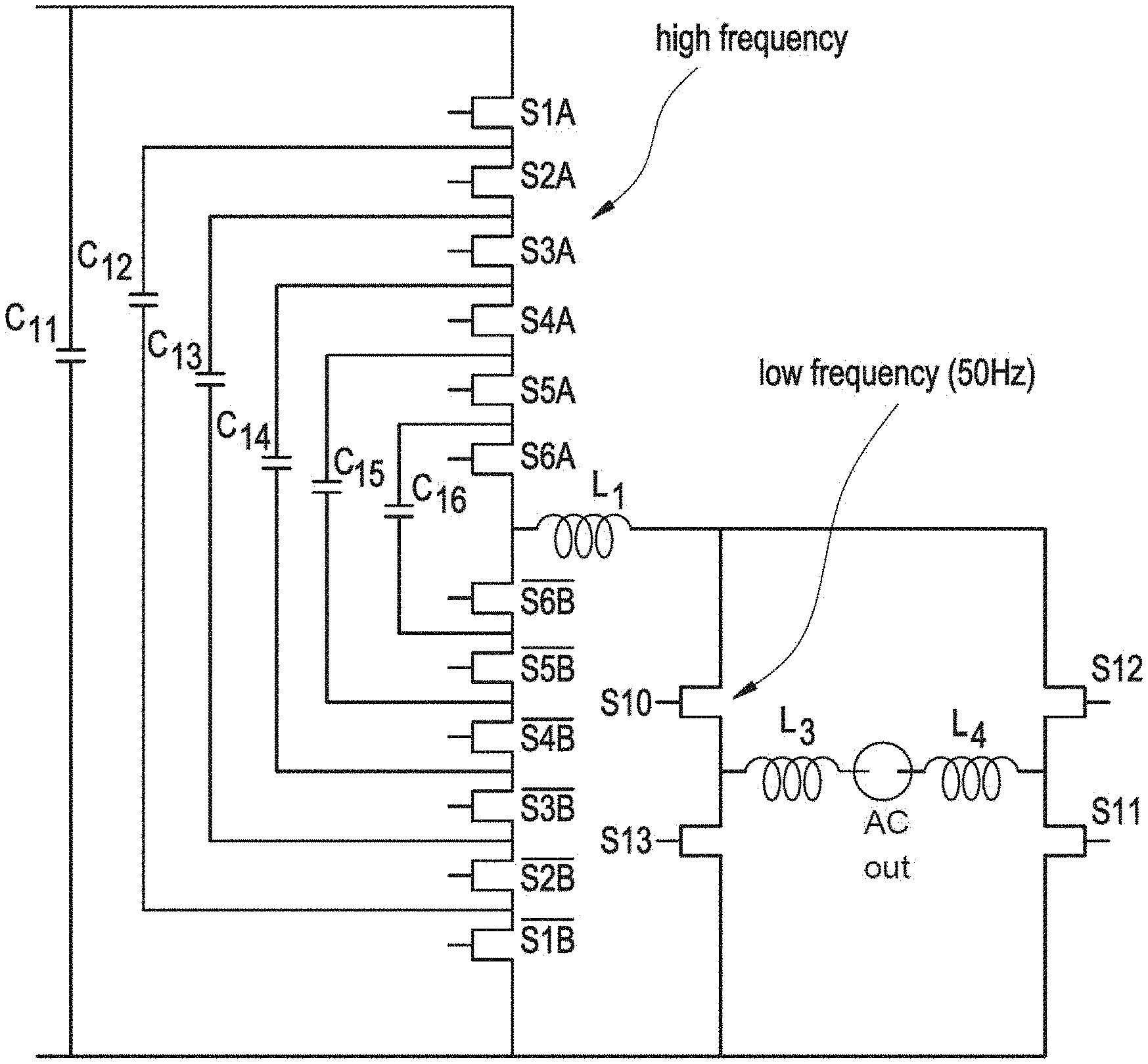
Referring to FIG. 1A, an exemplary multi-level inverter includes one, two, or more parallel connections each comprising a plurality of different switches disposed across a DC voltage. The switches may be coupled to a number of capacitors and/or inductors which may be utilized to smooth a sine-wave of an AC output of the inverter. For example, a plurality of switch banks S1A-S6A, S6B-S1B, S1C-S6C, and/or S6D-S1D may be disposed in any suitable configuration such as that shown in FIG. 1A. Each of the banks of MOSFET transistors may be variously configured to include two, three, four, five, six, seven, eight, nine, ten, eleven, twelve or more transistors.
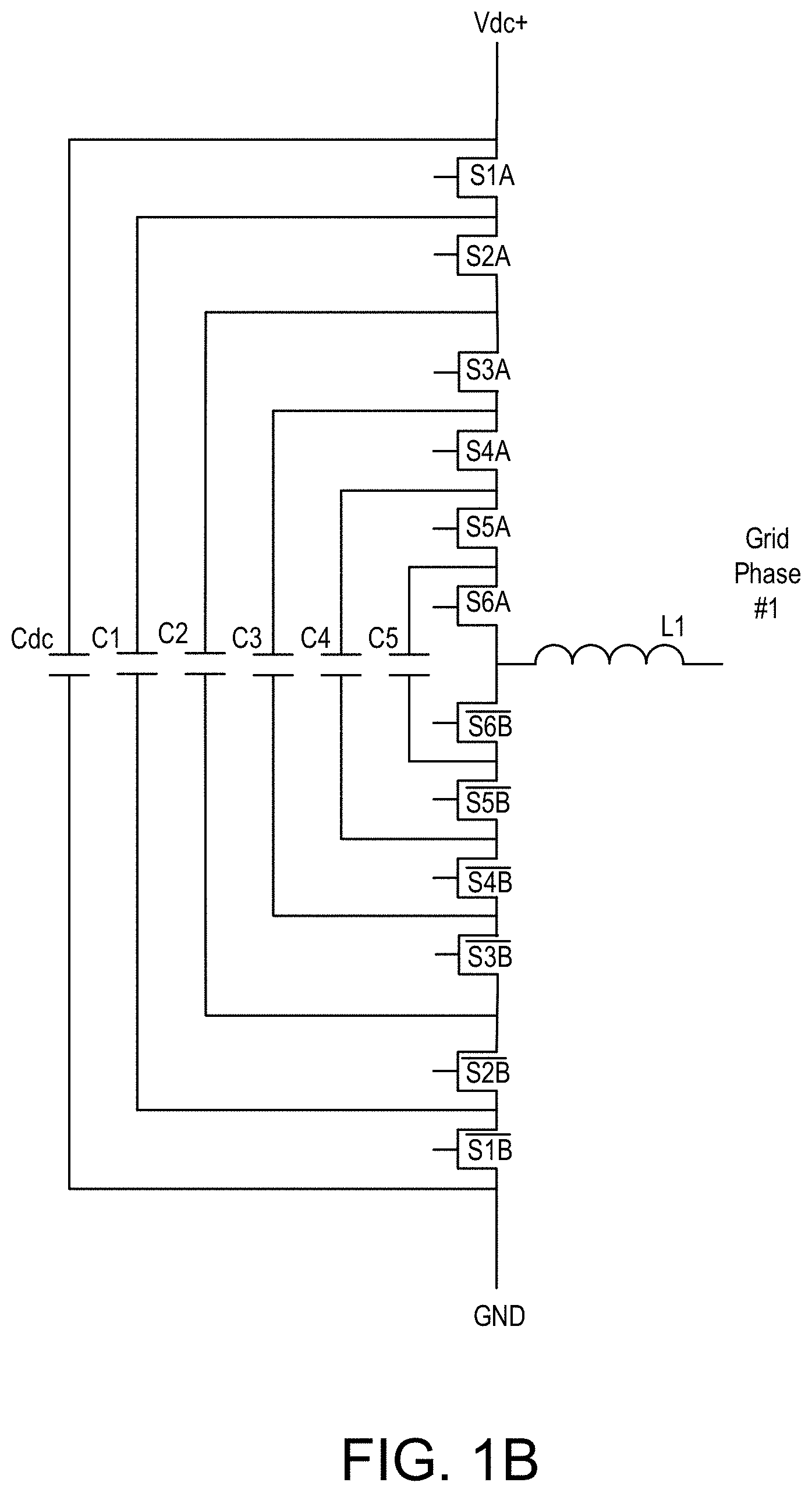
FIG. 1B illustrates half of the circuit illustrated in FIG. 1A. In various embodiments, during steady-state operation the capacitor voltages (C1, C2, C3, C4, and C5) average at *Vdc, 4/6*Vdc, 3/6*Vdc, 2/6*Vdc, 1/6*Vdc respectively (e.g. multiples of 1/N, where N is the number capacitors or the number switches in a bank, assuming the capacitors are of equal value). For embodiments where the capacitors are not of the same value, steady-state average voltage across each capacitor will scale accordingly.
During periods when the inverter is not operating at steady-state, such as during start-up of the inverter or during standby of the inverter, some embodiments may pre-charge the capacitors to their steady-state operating voltages.
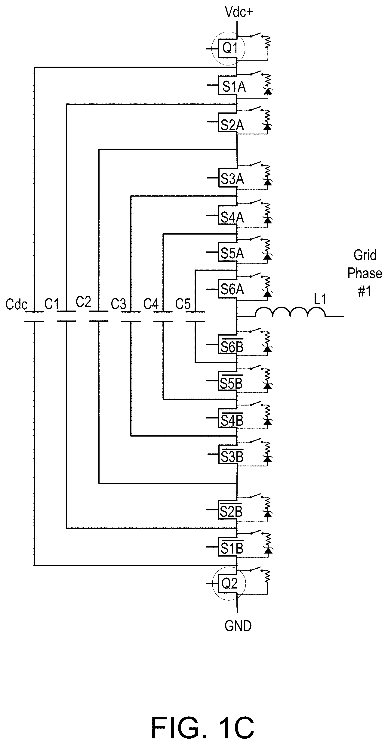
One embodiment for pre-charging capacitor voltage during non-steady-state operation of the inverter includes switching series zener diodes and resistors in parallel to each of the MOSFETs as shown in FIG. 1C. The capacitors are charged according to these resistor dividers, with the zener diodes protecting the MOSFETs from over-voltage. The zener diodes and resistors can be switched off once the capacitors are charged to their voltages for steady state operation of the inverter. In some embodiments, switches Q1 and Q2 may be added, each with a parallel bypass resistor path that can be optionally switched. During charging, Q1 and Q2 can be switched OFF and the parallel bypass switched ON (if a switch is present), such that the resistors in the parallel bypass path to Q1 and Q2 can limit the charging current from Vdc. Once charged, Q1 and Q2 can be switched ON, for normal operation of the inverter. When this option of Q1/Q2 is used, the parallel path to Q1 and Q2 may optionally include series zener diodes.
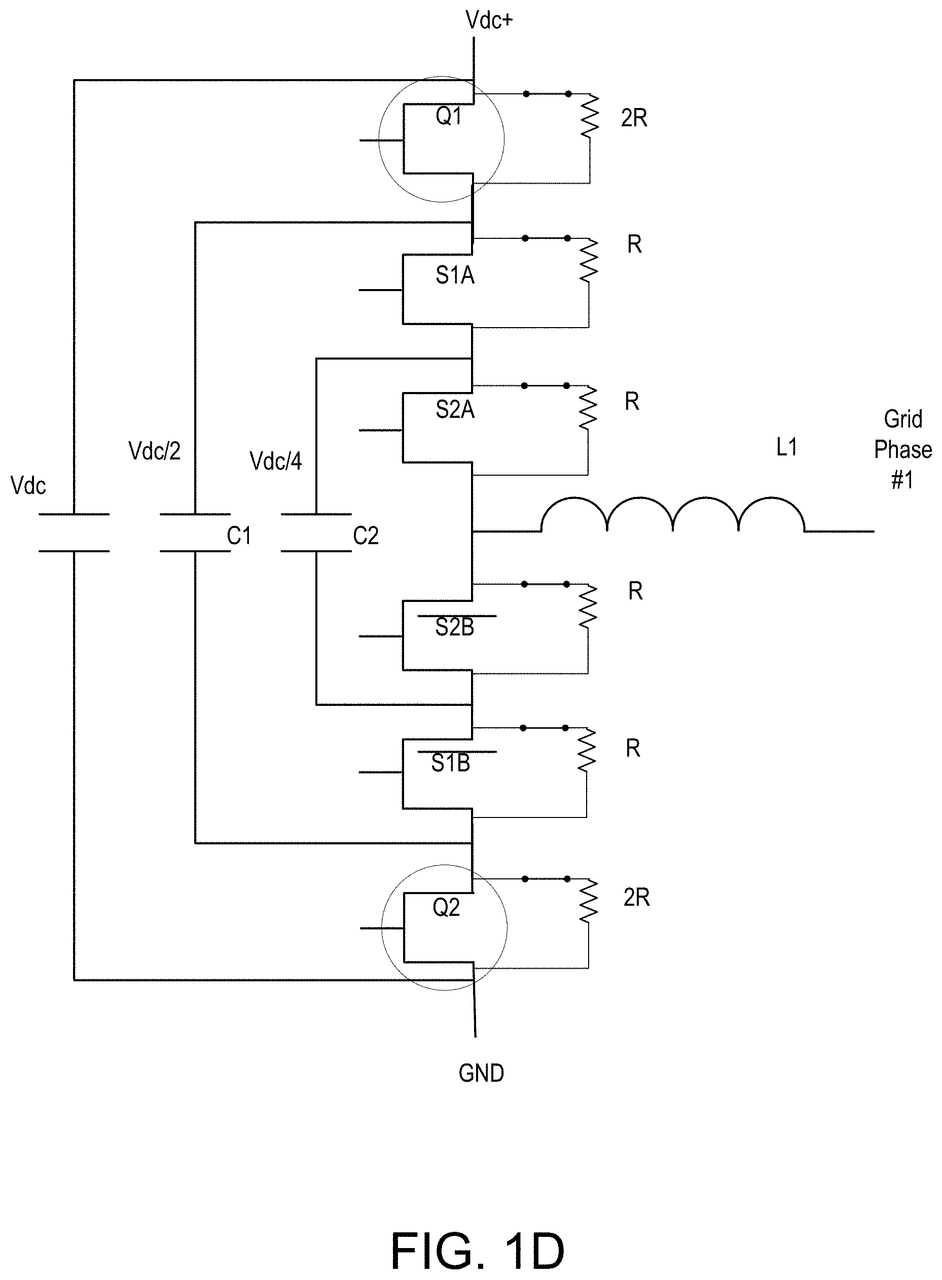
FIG. 1D illustrates another embodiment where N=2 (e.g., two MOSFETs in series). Q1 and Q2 are added in this implementation for operation in the pre-charge process as described with respect to FIG. 1C. In this embodiment, the zener diodes are eliminated from each parallel resistor path. In one example, with the resistance across Q1 and Q2 equaling 2R and the resistance across each inverter switch S1A, S2A, S1B, and S2B equaling R, voltages of Vdc/2 and Vdc/4 are generated with no current draw from the output (as is the case prior to steady-state operation).
Once the capacitors are pre-charged, the inverter may operate in steady-state with the timing shown in FIG. 2A, for example, or with other various timings. Referring to FIG. 3, each of the switches may be controlled by an output from a processor 10 (e.g., logic, one or more processor(s), controls, state machine, controller, microprocessor, software driven control, gate array, and/or other controller). In this embodiment, switch bank A comprises a series of FET transistors S1A-S6A (e.g., 20 v, 40 v, 60 v, 80 v, 100 v, 120 v MOSFET transistors) connected together in, for example, a source to drain configuration to form a first switching bank; switch bank B comprises a series of FET transistors S1B-S6B (e.g., 20 v, 40 v, 60 v, 80 v, 100 v, 120 v MOSFET transistors) connected together in, for example, a source to drain configuration to form a second switching bank; switch bank C comprises a series of FET transistors S1C-S6C (e.g., 20 v, 40 v, 60 v, 80 v, 100 v, 120 v MOSFET transistors) connected together in, for example, a source to drain configuration to form a third switching bank; switch bank D comprises a series of FET transistors S1D-S6D (e.g., 20 v, 40 v, 60 v, 80 v, 100 v, 120 v MOSFET transistors) connected together in, for example, a source to drain configuration to form a fourth switching bank. While six 80 volt FET transistors are used for each switch bank in this example, either more and/or less transistors can be utilized with different voltages e.g., 20 v, 40 v, 60 v, 80 v, 100 v, 120 v. For example, where 12 transistors are utilized in each switching bank, the voltages across those transistors may be adjusted to a suitable voltage such as 40 volts and the switching frequency of the transistors within one cycle may be increased from the example where only 6 transistors are utilized (e.g., switching each transistor at twice the rate).
Referring to FIG. 2A, each of the MOSFETs may be controlled to switch using a high frequency (e.g. around 200 kHz in this example) while still having low switching losses compared to other switch technologies. As shown in FIG. 2A, for this example, the MOSFETs are switched according to the duty cycle ratio (which changes according to the sine-wave) in the following simple manner (shown for six MOSFETs in series), where each MOSFET in series is shifted sequentially by 1/6 of the switching period. The specific timing shown in FIG. 2A is an example of the required duty cycles and a variety of different timings may be used that may have similar or different switching performance.
The duty cycle of the control signals may be varied according to required conversion ratio of the inverter, which may include a full range of duty cycles starting from 0 and ending up at 1 throughout, for example, a 50/60 Hz sine wave. When the required duty cycle D is smaller than T/N, the switch timing does not have any overlap as shown in FIG. 2A. When the required duty cycle is higher than T/N, the control signals start to overlap up to point where there is a full overlap between all control signals at the duty cycle of 1 (all switches are ON constantly).
FIG. 2B illustrates a more detailed diagram of low duty cycles where there is no overlap. The figure includes both control signals S1 through S6 respectively for switches S1A-S6A and signals S1.about. through S6.about. respectively for switches S1B-S6B.
When there is no overlap of the control signals, only one out of six MOSFET is ON (i.e., closed) on the high-side while only one out of six MOSFETS is OFF (i.e., open) on the low side as shown in FIG. 1E. FIG. 1E is illustrated with the MOSFETS represented as switches, with switch states corresponding to signal S1 On in FIG. 2B. As shown by the dotted line, the current flow is from Vdc+ towards the output (Grid phase #1) while passing through the MOSFETs that are ON and passing through capacitor C1, resulting in C1 charging with some ripple current. Since C1 is charged with *Vdc the total output voltage in this case, the output voltage is Vdc- *Vdc=1/6*Vdc. When S1 goes off in FIG. 2B, S1=S2=S3=S4=S5=S6=0 which yields an output voltage of 0. Subsequently S2 will be on resulting in an output being the voltage difference between C1 and C2 ( *Vdc- 4/6*Vdc=1/6*Vdc). The pattern continues with 1/6*Vdc at the output occurring when each switch is turned on. Therefore, during the multiplexing between the on state of one switch and the off states, any voltage between 0 to 1/6*Vdc can be generated with PWM. This occurs for any case where the duty cycles are below 1/6, resulting in no overlap in ON signals between the MOSFETs.
FIG. 2C illustrates another example of a timing diagram with a high duty cycle where there is an overlap between all the MOSFETs besides one (when the duty cycle is higher than ).
As another example, FIG. 1F shows the switch states and current flow when there is an overlap between S1 and S2 (due to a duty cycle between 1/6 and 2/6 in this specific example. The dotted line again shows the path from Vdc towards the output, and in this case capacitor C2 is used. C2 is charged to a voltage of 4/6*Vdc, and therefore the output is Vdc- 4/6*Vdc= 2/6*Vdc. In this specific case the PWM multiplexing will be between 1/6*Vdc (as in the previous case of a single MOSFET in the ON state) and 2/6*Vdc, corresponding to a duty cycle that is between 1/6 and 2/6.
Another example of a duty cycle between 1/6 and 2/6 is shown in FIG. 1G where two capacitors are used in the same path towards the output. This is a case of overlap between S2 and S3, again for duty cycles between 1/6 and 2/6. The path goes through capacitor C1 (Vdc* ) and capacitor C3 (Vdc* 3/6) but in different directions, such that the output voltage is Vdc* -Vdc* 3/6=Vdc* 2/6, which is the same as the previous case. Now, however, capacitor C3 gets charged with ripple current and capacitor C1 gets discharged with ripple current. It is noted that capacitor C1 was charged in the previous case now gets discharged and eventually can ripple about the same value ( Vdc).
In various embodiments, the basic timing diagram that was presented is built such that the same duty cycle is used for all six MOSFETs and there is a phase delay of T/N between these MOSFETs which will eventually yield the required voltages according to the duty cycles while keeping all of the capacitors charged and discharged to the same average value.
As further examples, FIGS. 2D and 2E illustrate timing diagrams for low duty cycles and high duty cycles, respectively for the circuit implementation of FIG. 1D based on N=2 (two MOSFETs in series). For each of these cases (low duty cycle, high duty cycle), there are several states (00, 01, 10, 11) where 0 and 1 denote which of the switches [S1,S2] are ON or OFF (and S1.about. and S2.about. follow them as complementary signals).
For states 00 (S1 and S2 OFF) and 11 (S1 and S2 ON), current flows directly from Vdc or GND, without going through the capacitor C2 (also identified as the flying capacitor). However, states 01 and 10 flow current into the capacitor where each of these states is opposite in the current direction as shown in FIGS. 1H and 1I. In the timing diagrams shown FIGS. 2D and 2E, the dwell time in state 01 and state 10 is the same and therefore the capacitor C2 gets charged and discharged by the same portion and eventually stays balanced. However, due to possible mismatches and drifts there is a need to actively tune the capacitor voltage.
One method for balancing the flying capacitor drifts is by changing the dwell time of each of the states 01 and 10 such that in average we will have the required dwell time which fixes the required duty cycle but the dwell time difference will allow more charge than discharge or the opposite. FIG. 2D illustrates a timing diagram that has a 20% duty cycle for each S1 and S2 signals. In FIG. 2F, the timing of S1 and S2 are illustrated, with the timing of S1 being changed to a 30% duty cycle and the timing of S2 being changed to 10% such that the average is 20% as required but a drift of the capacitor C2 voltage is towards its required steady state value.
Another method for balancing capacitors is to change the timing diagram such that the state 01 is switched to more times than state 10. This type of balancing solution is more generic and can be used more easily in cases of more than two states (e.g., in the case of more MOSFETs in series) where a particular state is chosen in any time in order to drift the flying capacitors to their pre-charged steady-state value.
In addition to the conduction and switching losses advantages discussed above, another major benefit of the embodiment shown herein is the reduction of passive components (e.g., main choke and output filter sizes). Due to the multi-level voltages, a factor of N (e.g. 6 in the example) can be reduced in size/cost. In addition, the effective frequency within the main choke is N times the switching frequency (e.g. 6*200 kHz in this case). The result of embodiments in accordance with this example is that the main choke can be smaller by a factor of N{circumflex over ( )}2 (e.g. 36) relative to a standard design using 200 kHz. Since usual inverters use much smaller switching frequencies (e.g. 16 kHz) due to limitations of the 600V switches, the overall gain in the main choke size is 200 kHz/16 kHz*36=450 which makes it negligible while in a standard inverter it is about 20% of the size and cost of the inverter. A similar calculation can be made for the output filter showing even greater advantage.
Embodiments of the present invention switch at a higher frequency such as 16 KHz or 33 KHz or preferably 50 kHz, 100 kHz, 150 kHz, 200 kHz, 250 kHz, 300 kHz or even higher), and the manner in which the switches are modified in accordance with, for example, FIGS. 2A-2F. The gain in accordance with inverters of the present examples gain a factor of n squared. This unusual result is achieved in part by switching only one component at a time instead of switching all of them in one cycle. Using low voltage MOSFETs, it is possible to switch all of the switches in the same output voltage cycle while still achieving comparatively low switching losses which allows further gains and efficiencies.
Usually about 20% of both size and cost of an inverter are related to the main choke. In embodiments described herein, increasing the frequency to, for example, 6*16 kHz and increasing the number of switches to 6 can result in an additional gain factor of 36 relative to the original 16 KHz because of the multi-level components. In these embodiments, the cost of the main choke can be as little as one percent or even less than that of the overall inverter cost. In addition, because of switching method described herein, the inverter will be much more efficient and also the production of the output voltage will be much better which gains substantial efficiency. It means that the enclosure and the inverter can be dimensionally much lower and therefore a much smaller and cheaper enclosure can be used. The size and cost of the enclosure is reduced both because of reduction of the main choke, reduction in the filter, and because of improved efficiency, which provides a smaller and more compact enclosure.
The control shown in FIGS. 2A-2F has been demonstrated to have substantial efficiencies over conventional control circuits. For example, the control illustrated in FIG. 2A allows the switches S1A-S6A, S6B-S1B, S1C-S6C, and S6D-S1D to be switched all within one period, in this embodiment with the switching of switches in one bank to be offset as shown in FIG. 2A. In these embodiments, the switches operate six times higher than other control mechanisms.
Referring again to FIG. 1A, an inverter is may comprise two halves with symmetry on each side of the inverter. In the embodiment of FIG. 1A, there are 4 banks of six switches each for 24 switches which operate at a lower voltage (e.g., 80V) and a higher frequency (e.g., 200 kHz). The higher frequency switching allows staggered switching of each switch in each bank (e.g., all six switches) in one cycle, which is six times faster than conventional modulators.
For voltage, where the absolute voltage is around 350V (which may be a voltage received from a DC source such as a bank of solar panels), this voltage may be utilized to produce an AC voltage of, for example, 230V. The switching elements in each bank when coupled with the capacitors C1-C5 and C6-C10 may be switched such that the voltages across switching banks A and B and switching banks C and D may sum to a voltage of approximately 350V in this example. Because the voltage across any one switch can be much lower than 350V because the voltage is spread over each of the switch/capacitor combinations, the voltage of the switches can be much smaller (e.g., 350 divided by 6 which or around 60V). This voltage can be made lower and/or higher depending upon the number of switches in each bank.
Referring to FIG. 2A-2F, the switches may be configured to switch all during the same cycle. For example, the switches may each be switched at, for example, 200 kHz. This allows each switch to turn "on" for a predetermined period such as 1/200 kHz or around 5 microseconds, during which time each switch turns on and off. In a conventional multi-level inverter, only one switch will switch at one cycle of one of the 16 kHz. However, in embodiments described herein, the low voltage MOSFETs may be switched at a much higher rate (e.g., 200 kHz) and additionally all of the switches in one bank may be switched during the same period. This example effectively increases the speed to 6 times the switching period, without actually increasing the switching frequency. Further, the design is scalable in that it can be increased more and more by adding more transistors to the switching banks; the multi-level switching in each bank allows the switching to increase in frequency without driving the MOSFET faster (e.g., six times faster).
This is an advantage of multi-level inverters in the examples herein in that you can switch six, eight, ten, twelve, or more times faster depending on the number MOSFETs in a series in each switching bank. One advantage associated with certain embodiments, is that it is possible to switch 6, 8, 10, 12, or more times faster by switching all of the MOSFETs during the same period, without actually switching any one of the MOSFETs faster than the original speed. This is a structural advantage cannot be achieved in inverters today because the switching ability of conventional designs cannot achieve this result. By controlling the control switches to operate in accordance with FIGS. 2A-2F, for example, it is possible to super charge a multi-level inverter to switch all the switches during the same cycle time and thus achieve an effective frequency of, for example, six times higher without actually switching any of the switches (e.g., MOSFETs) at a higher frequency.
Because of the higher switching frequency in accordance with the present embodiments, in addition to a smaller choke, the capacitors between the switches will be smaller. This is part of the size and cost reduction. Additionally, the inductors L1 and L2 are also made smaller. In general, there are many components that shrink by going to a higher frequency, which is being increased, also by the factor of 36.
Again referring to FIGS. 2A and 3, the control into S1A-S6A is inverted from the control input into switches S1B-S6B (e.g., when S1A is closed, S1B is open). With respect to switches S1C-S6C, the control inputs to these switches are inverted from the control inputs to switches S1A-S6A (e.g., when S1A is closed, S1C is open). With respect to switches S1D-S6D, these switches have the same control input as those of switches S1A-S6A (e.g., when S1A is closed, S1D is closed). While the processor needs to control 24 switches, because banks A and D receive the same six control signals and banks B and C receive the opposite six control signals, it is possible to have only six output control signals input respectively to each of S1A-S6A and S1D-S6D and the inverse of these six control signals sent to S1B-S6B and S1C-S6C.
In these embodiments, S1C-S6C are inverted and S1D-S6D are not inverted with respect to the control input signal. Further, S1A-S6A are not inverted and S1B-S6B are inverted. Thus, 24 switches may be controlled with only six different control outputs from the processor. See, for example, the exemplary control structure shown in FIG. 3.
Various alternate embodiments may also be employed. For example, referring to FIG. 4, an alternate embodiment is shown which includes a single leg of multi-level MOSFETs that may be configured to generate a rectified sine-wave by performing DC/DC operation (buck) during a sine-wave cycle. In this embodiment, the output of the leg may be inverted by a low-frequency full-bridge operated at AC line frequency (e.g., 50 Hz).
With this variation, the switching losses at the high-frequency are reduced by a factor of two relative to a full-bridge implementation and the conduction losses are a combination of the single multi-level leg and the slow-switching full-bridge. It is possible to reduce the conduction losses of the slow-switching full-bridge by using improved components (e.g Super-junction MOSFETs or a series-stack of low-voltage MOSFETs) while not increasing switching losses due to low switching frequency.
Another benefit of this variation is that the component cost may be further reduced since there is only one multi-level leg with all the drivers and balancing capacitors and the full-bridge components can be made much cheaper than the cost of another multi-level leg.
Again referring to FIG. 4, the output of the high frequency stage is a rectified sine-wave (e.g., whenever the sine-wave is positive, it is the same, whenever the sine-wave is negative, it's still positive). The high frequency stage may be configured to generate a sine-wave but it is always positive. The low frequency stage inverts the rectified sine-wave to positive and negative, to create a true sine-wave. The low-frequency stage may be configured to invert the signal whenever it is needed. In this embodiment, the low frequency stage has a number of switches such as four switches S10, S11, S12, S13. In this example, the positive cycle of the sine-wave can be achieved by having the top-left S10 and bottom right S11, switching to on. When the other half of the signal is processed, the control can switch on the other diagonal, e.g., the upper right switch S12 and the bottom left switch S13 to invert the signal completing a sine-wave. These switches may be controlled via a processor such as processor 10 shown in FIG. 3.
The use of MOSFETs for the first high frequency stage controlled as discussed herein in order to shape the rectified sine-wave is another example of the invention. The advantages discussed above with respect to FIGS. 1A-1I, 2A-2F, and 3 can be achieved in the embodiment of FIG. 4 with only 16 switches as opposed to the 24 switches of FIG. 1A. Thus, substantial advantages can be achieved and further reduced costs and components.
Still another embodiment is shown in FIG. 5. In the embodiment of FIG. 5, S1G-S6G and S6H-S1H and C17-C22 operate above as discussed with respect to FIGS. 1A-1I, 2A-2F, and any of the other embodiments discussed below. In this embodiment, a single phase inverter adds an additional multi-level leg at the input of the inverter. In other words, the circuit of FIG. 5 may in FIG. 1A (or any of the other embodiments) be connected across the Vdc (e.g., 350 v) input (e.g., C17 of FIG. 5 is connected across the 350 v input bus). As further discussed herein, this architecture may be referred to as the active capacitor concept. The additional leg may be configured to act to transfer capacitive charge between the DC link capacitor (C17) and the storage capacitor (C23) in order to compensate for the low frequency pulsation, such as a low frequency pulse of around 100 Hz. Since the storage capacitor C23 may be configured to fluctuate with full voltage swing, its size can be reduced considerably relative to the original size of the input bus capacitance. The size of C17 can be very small.
This type of solution for reducing the DC link capacitor C17 when implemented using multi-level topology with low-voltage MOSFETs as shown can be very efficient (0.2% losses) and therefore reduce both size and cost without a high impact on the performance.
In FIG. 5, the capacitor C17 on the input takes the difference between the output power and the input power. The input power is DC and the output power is AC. The output power is fluctuating and the DC power does not fluctuate because it is DC. Some capacitors absorb over/under power in view of sine-wave fluctuations. Usually, the input capacitor, on such an inverter is very big and can be 10 percent of the cost of the inverter. With respect to the embodiment shown in FIG. 5, instead of having a very big capacitor which is C17, using this embodiment, C17 can be very small and actually performing DC to DC conversion between C17 and C23 due to the low power MOSFETs and control switching topology discussed herein. For example, whenever there is too much power on the AC side, then C17 needs to provide more power, then it takes it from C23 and whenever there is too much power on the DC side, then C17 gives that redundant power to C23. So, everything is going back and forth between C17 and C23. But eventually it compensates for the difference between the DC power and the AC power. By using the techniques described herein of low-voltage multi-level component with the associated control, embodiments gain the ability to reduce the capacitances of the input of the inverter.
In still further embodiments, the capacitor C11 of FIG. 4 can be replaced with the circuit shown in FIG. 5 (e.g., e.g., connected to C17 of FIG. 5). With these examples, the modified FIG. 1A would now have 36 MOSFETs as opposed to 24 MOSFETs. Similarly, for the example where FIG. 4 is modified, the circuit would have 24 MOSFETs as opposed to 12 MOSFETs, but the large capacitor C11 is no longer present. Thus, the circuit shown in FIG. 5 can serve as replacement for the capacitor on the left-hand side of FIG. 1A (not shown) and/or for a replacement for the capacitor shown on the left-hand side of FIG. 4 (C11).
In still further embodiments, such as three phase embodiments, there may be more banks of MOSFET transistors. For example, referring to FIG. 1A, there may be additional banks of MOSFET transistors S1E-S6E and S1F-S6F and associated capacitors. These MOSFET transistors would be controlled in the same manner as the other legs and transistor banks discussed herein. In this example, instead of just two legs shown in FIG. 1A, one on the left and one leg on the right, you may have three legs similarly configured.
FIG. 6 shows another embodiment similar to the flying capacitor topology or the capacitor-clamped multi-level inverter topology shown in, for example, FIG. 1B or 5. In the configuration shown in FIG. 5, two banks G, H of series connected switches are connected to each other between a high voltage and a low voltage and capacitors C17-C22 are nested within each other between the two banks. The capacitors are nested within each other by connecting the ends between corresponding switches in each bank. For example, capacitor C18 is connected at a first end between S1G and S2G and at a second end between S1H and S2H. Similarly, capacitor C19 is connected at a first end between S2G and S3G and at a second end between S2H and S3H.
The circuit shown in FIG. 6 reduces the number of capacitors used in the circuit compared to the embodiment shown in FIG. 5. For example, capacitors C18, C20, and C22 from the circuit of FIG. 5 are absent in the circuit shown in FIG. 6. Each two MOSFET transistors in series may be considered as one switch with only one mutual PWM control signal. For example, switches S1I and S2I may be considered as one switch and be controlled by a single PWM control signal. Similarly, switches S3I and S4I, S5I and S6I, S6J and S5J, S4J and S3J, and S2J and S1J may be paired. Capacitor C25 is connected at a first end between S2I and S3I and at a second end between S2J and S3J. The series connection of these two MOSFET transistors allows spreading of the voltage stress between the two MOSFET transistors assuming they are balanced at OFF state and transition times. This balancing may be accomplished with either by biasing the drives of any two adjacent MOSFETs or by still keeping C18, C20, and C22 from FIG. 5 with small capacitance and driving the two adjacent MOSFETs (e.g., S1I and S2I, S3I and S4I, S5I and S6I, S6J and S5J, S4J and S3J, S2J and S1J) at similar timing such that C18, C20, and C22 will be kept balanced for the transition period only. The implementation of FIG. 6 may be applied to any of the embodiments herein.
FIG. 7 shows another embodiment that is able to reduce the capacitance of one of the flying capacitors. In this embodiment, standard multi-phase techniques are used by having parallel switches in the middle of the phase leg such that each parallel switch leg is switched in a time-shifted manner versus the other switch leg in order to provide multi-phasing (e.g. 180.degree. in the shown case of two parallel phase legs). In FIG. 7, the parallel switch legs may be a first leg of switches T1B, T1C, T2B, T2C and a second leg of switches T3A, T3B, T4A, T4B. Multi-phasing enables reduction of the ripple voltage in the flying capacitor C29 by a factor of four, which allows the reduction of the capacitance of the flying capacitor C29 by the same factor. Additionally, the phase inductor L6 as shown in FIG. 6 can be split into two inductors L8, L9 where mutual coupling eventually allows the reduction of the inductors' size below the original required inductor L6 in the case where multi-phasing is not used.
Multi-phasing may be used between parallel phase legs in order to achieve benefits in the input capacitance and output inductance. In the embodiment shown in FIG. 7, the multi-phase technique is employed on a sub-set of the phase leg in order to reduce the flying capacitors and not just the main capacitance of the whole phase leg.
More generally, multi-phasing can be applied to each of the flying capacitors separately and then also applied to the whole leg thereby achieving a hierarchical structure of multi-phasing.
FIG. 8 shows another embodiment that may be applied on a high voltage boost converter (e.g. as a front-end sub-system of a photovoltaic panel inverter or not necessarily related to an inverter) utilizing the multi-level inverter topology and using low-voltage MOSFET transistors at high switching speeds with staggered timing in the same manner as described herein.
This structure is split into two halves where each half of the structure handles half of the input voltage by using multi-level techniques (in the case of FIG. 8, three-level). It can be of course extended to higher numbers of switches in series thereby increasing the number of levels in each half. For example, in FIG. 8, the switches T5A, T5B, T6A, T6B may form the first half, and the switches T7A, T7B, T8A, T8B may form the second half. The control signals to switches T6A-B may an inverted version of the control signal to switches T5A-B, respectively. For example, the control signal to switch T6A may be inverted from the control signal to switch T5A, and the control signal to switch T6B may be the inverted version of the control signal to switch T5B. The timing of the control signals to the A switches (T5A, T6A) may be the delayed version or the same as the controls signals to the B switches (T5B, T6B). Control signals similar to the first half may be applied to the second half. For example, the control signals to the A switches (T7A, T8A) may be inverted versions of each other, and the control signals to the B switches (T7B, T8B) may be inverted versions of each other. The control signals to the T7 switches may be the same or different than the control signals to the T5 switches. Similarly, the control signals to the T8 switches may be the same or different than the T6 switches.
FIG. 9 shows another embodiment reducing the number of capacitors used in the circuit. For example, capacitors C18 and C19 from FIG. 5 or C1 and C2 from FIG. 1B may be removed or used as a small capacitance for balancing purposes such that the three switches S1K-S3K above capacitor C38 in FIG. 9 and the three switches S1L-S3L below capacitor C38 become low frequency switches that can operate at, for example, 50 Hz complementarily while the other 6 switches S4K-S6K, S4L-S6L connected to capacitors C38-40 act as fast switches (e.g., high frequency switches) using a flying capacitor control method as described herein where the control signals to the switches S4L-S6L are inverted versions of the control signals to the switches S4K-S6K.
FIG. 10 shows another version of a multi-level inverter circuit including an inter-phase balancing block. The circuit of FIG. 10 is similar to the circuit of FIG. 9 with the addition of the inter-phase balancing block B1. Similar to FIG. 9, the three switches S1M-S3M above capacitor C42 and the three switches S1N-S3N below capacitor C42 may be low frequency switches. Switches S4M-S6M, S4N-S6N may be fast switches using a flying capacitor control method described herein. The inter-phase balancing block B1 may be connected in parallel to capacitor C42 which is connected at each end between a low frequency switch S3M, S3N and a high frequency switch S4M, S4N. The inter-phase balancing block can share current over capacitor C42 to remove a low frequency (e.g., 50 Hz) ripple over capacitor C42 from the switches S1M-S3M and S1N-S3N being switched at 50 Hz. The circuit shown in FIG. 10 maintains seven levels since, in each 50 Hz half cycle, the circuit shown in FIG. 10 provides three different levels resulting in six levels in addition to the zero level.
The circuit shown in FIG. 10 may comprise a leg of an inverter. An inverter may contain several legs. For example, a single phase inverter may have two legs with the legs connected via the interphase balancing block B1. Specifically, capacitor C42 of each phase may be connected in parallel to the same interphase balancing block B1 or an inter-phase balancing block B1 shared with another phase. As another example, a three phase inverter may include three legs connected to each other via inter-phase bal
D00000
D00001
D00002
D00003
D00004
D00005
D00006
D00007
D00008
D00009
D00010
D00011
D00012

D00013

D00014
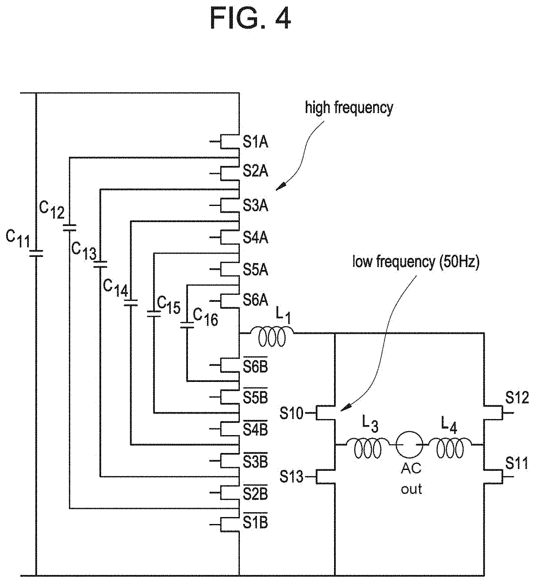
D00015
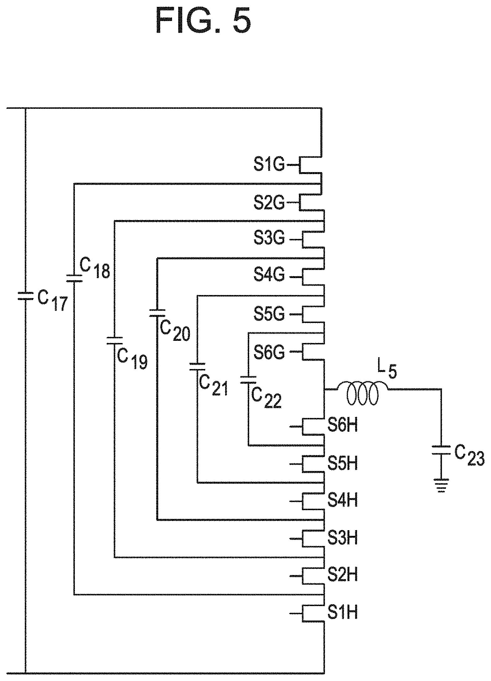
D00016
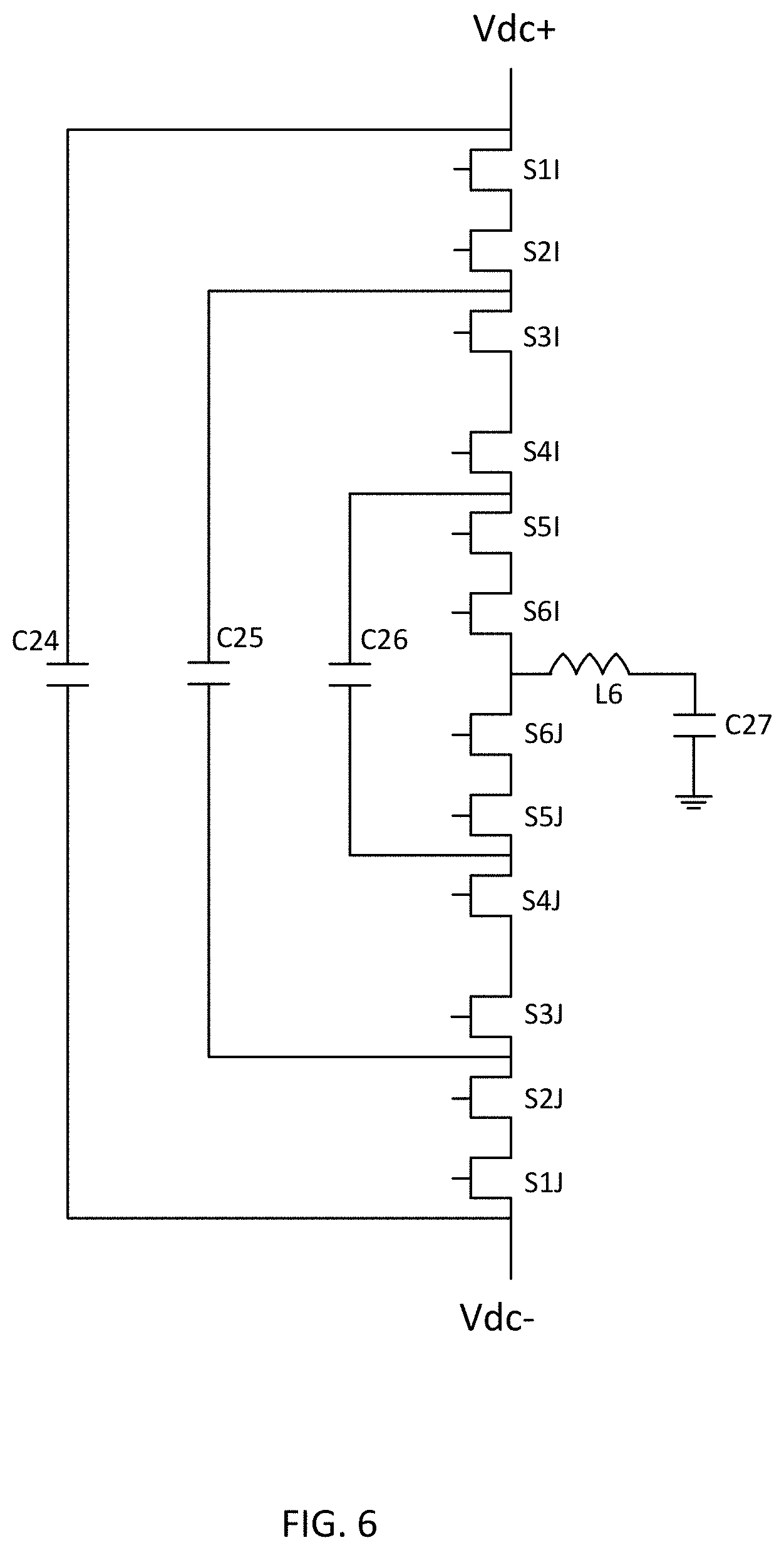
D00017
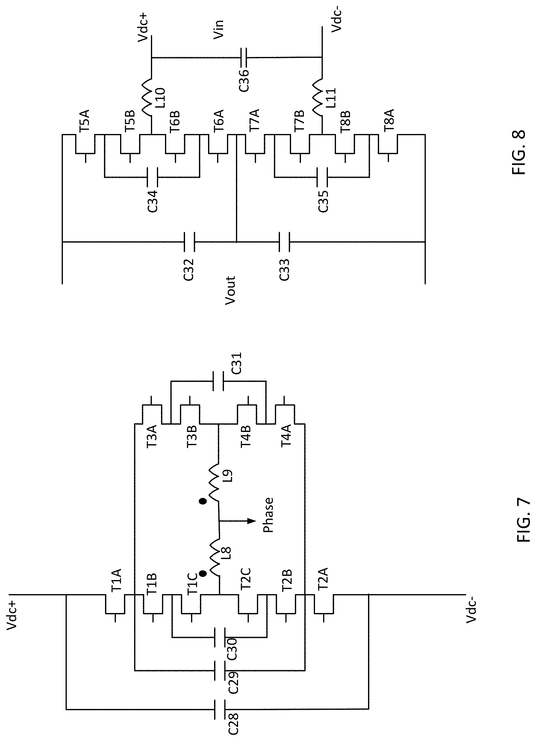
D00018

D00019
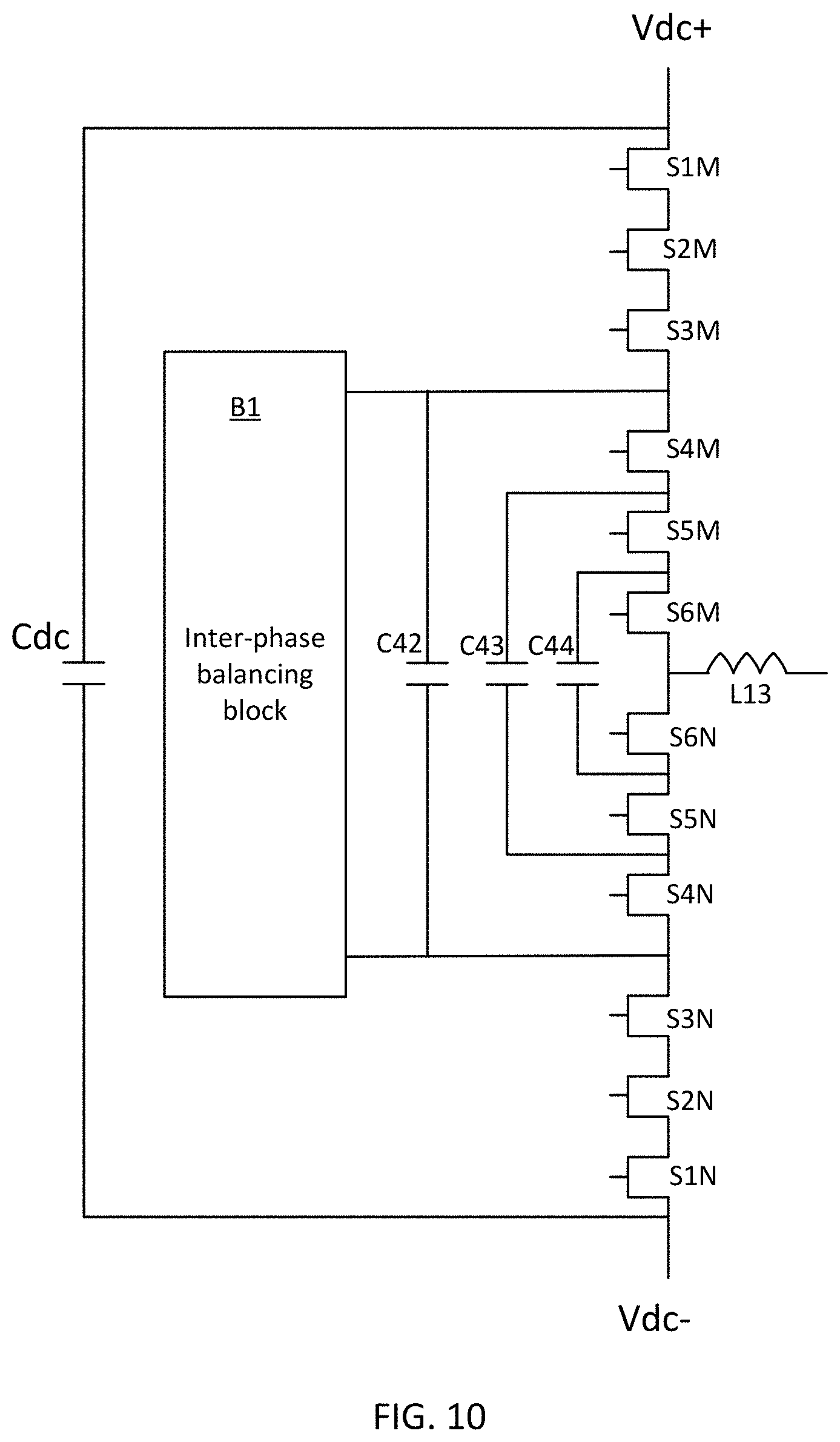
D00020
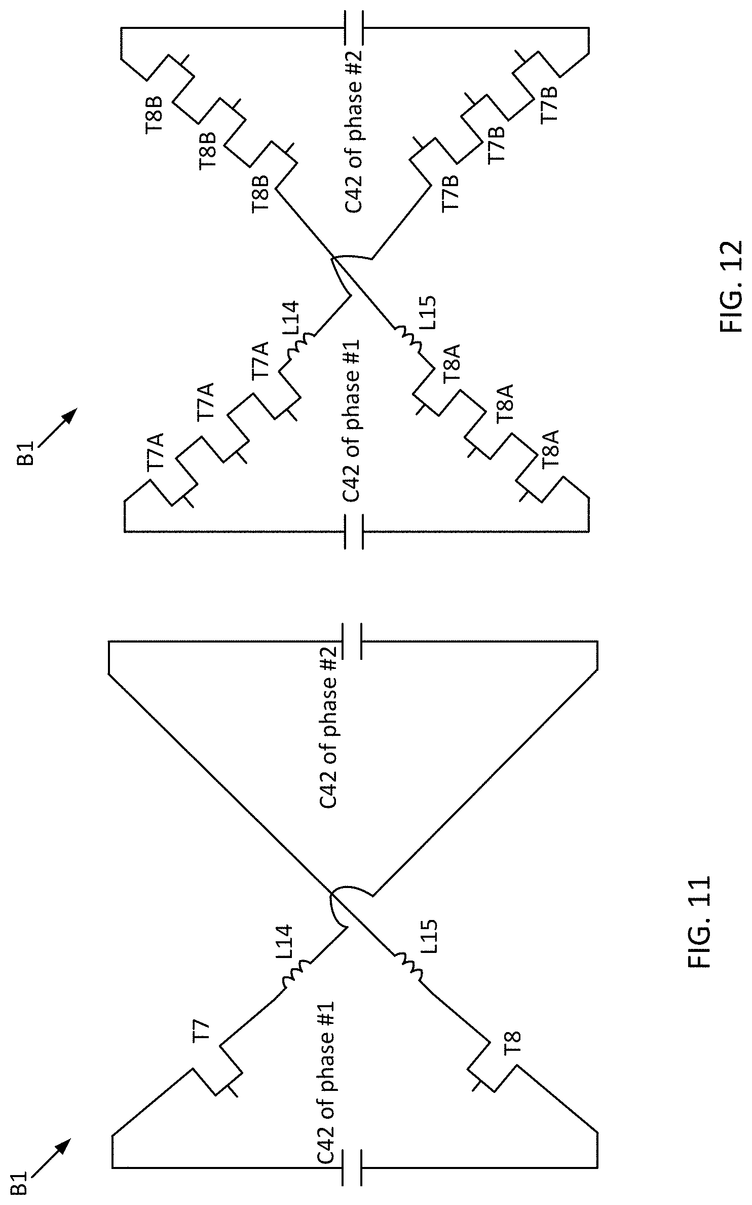
D00021

D00022

D00023

D00024
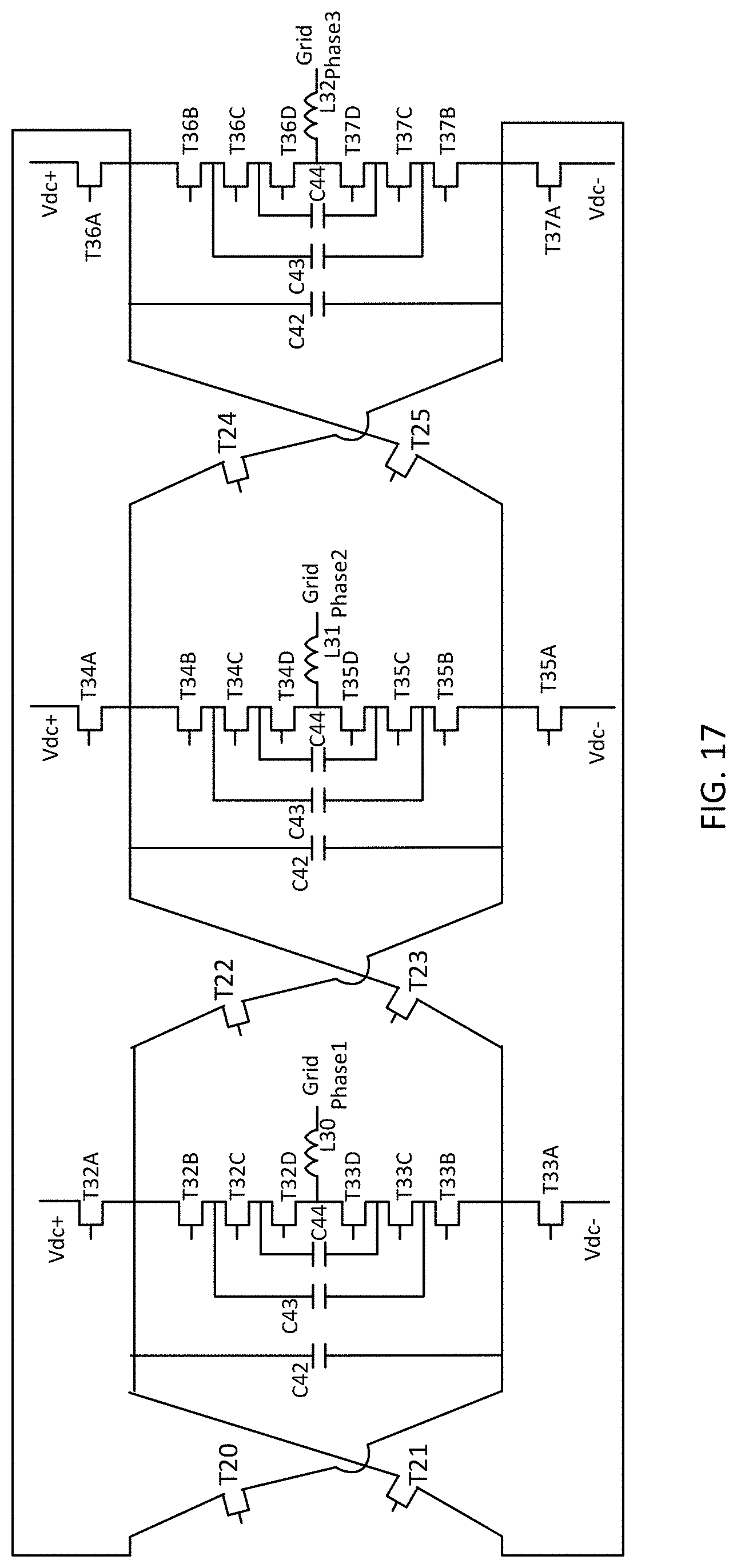
D00025
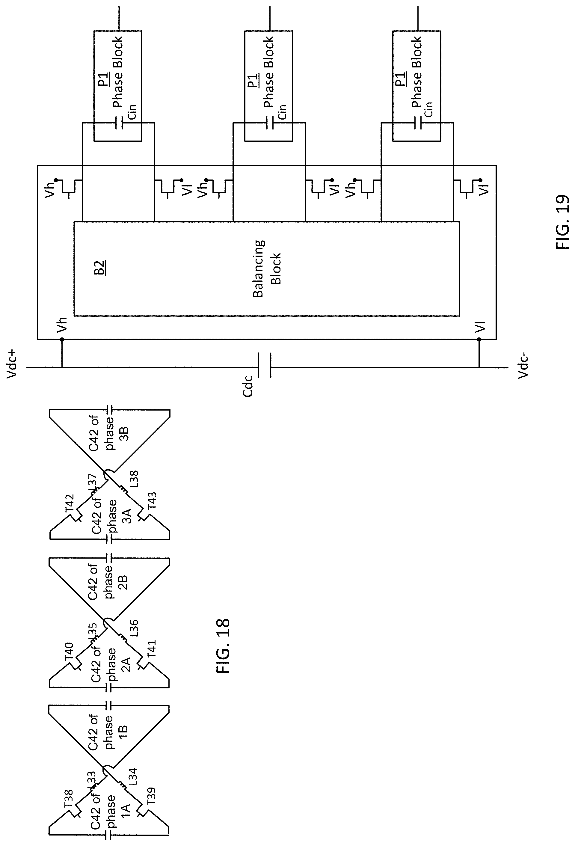
D00026
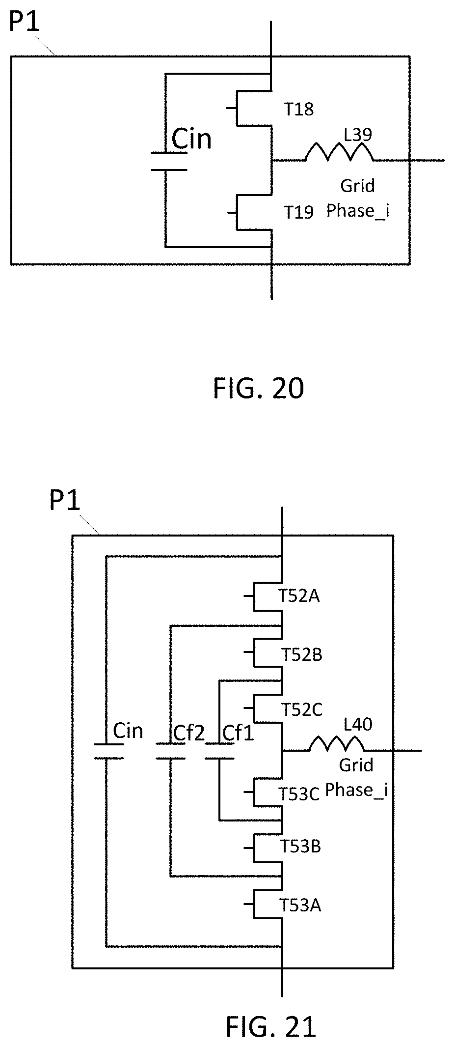
D00027
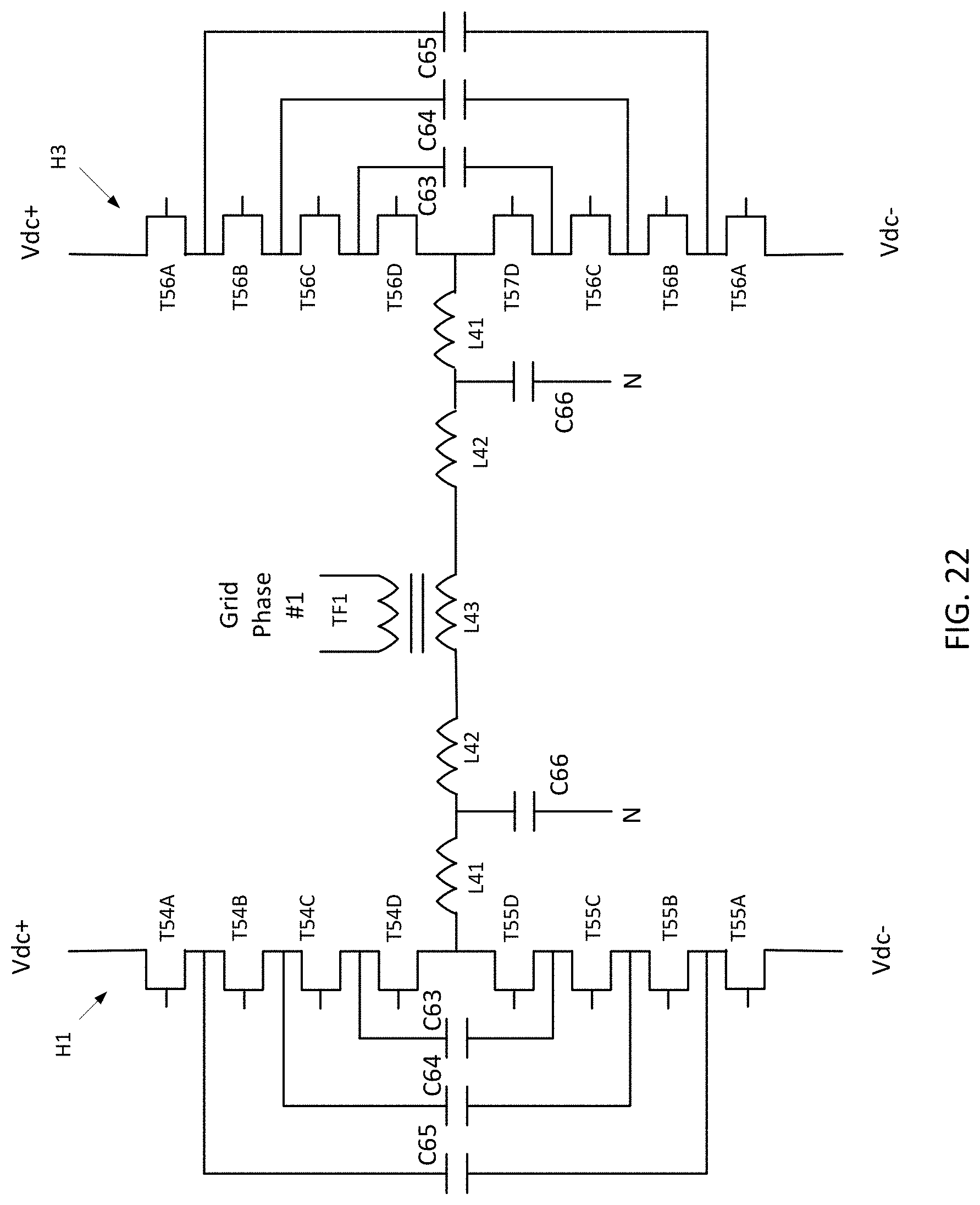
D00028

D00029
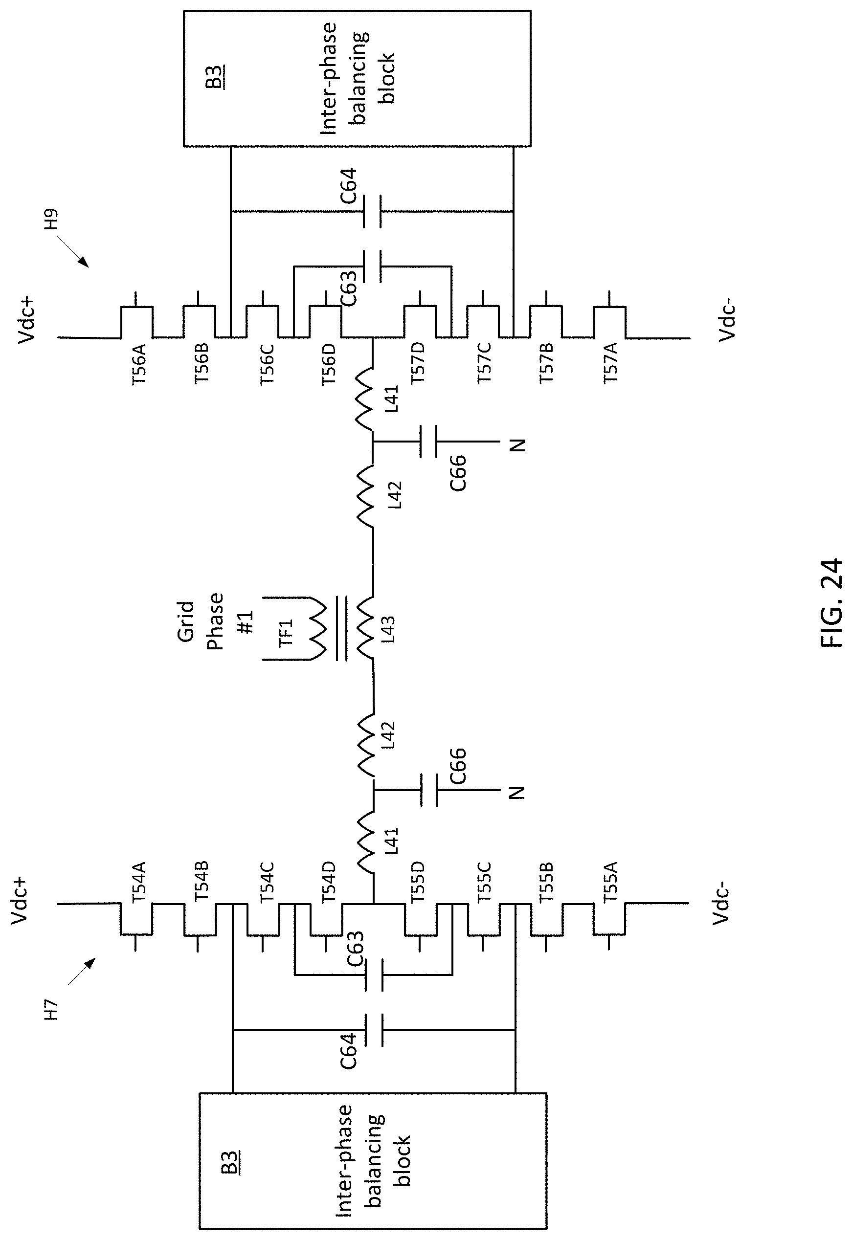
D00030
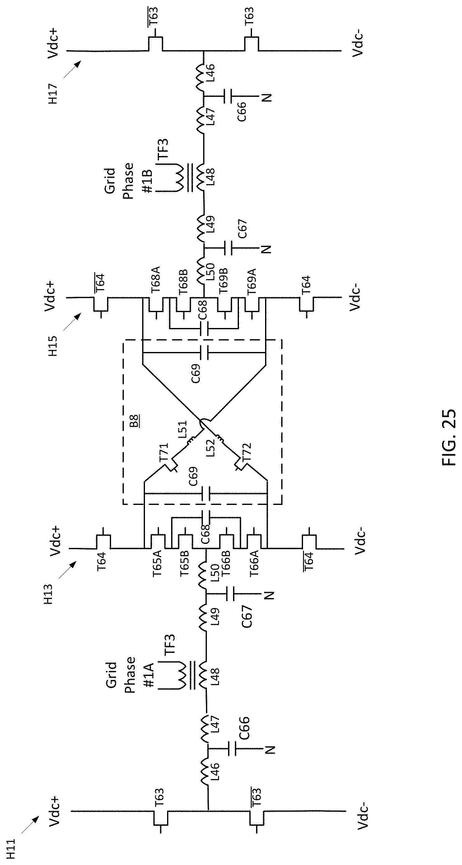
D00031
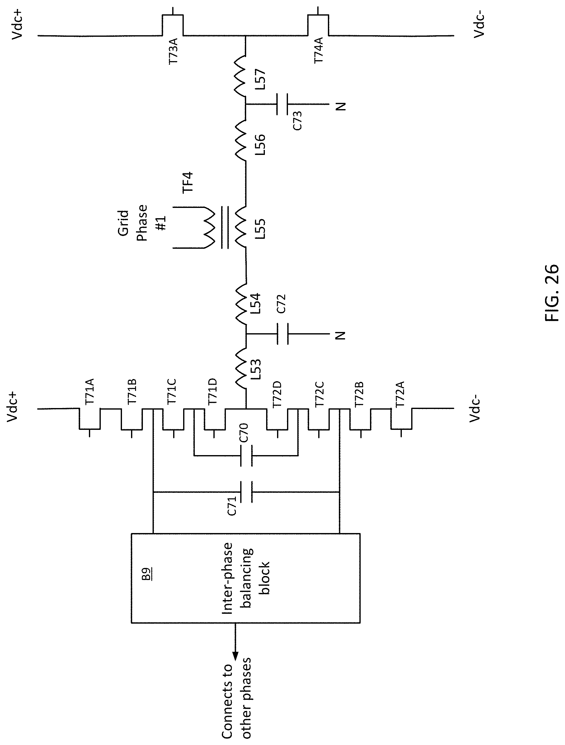
D00032
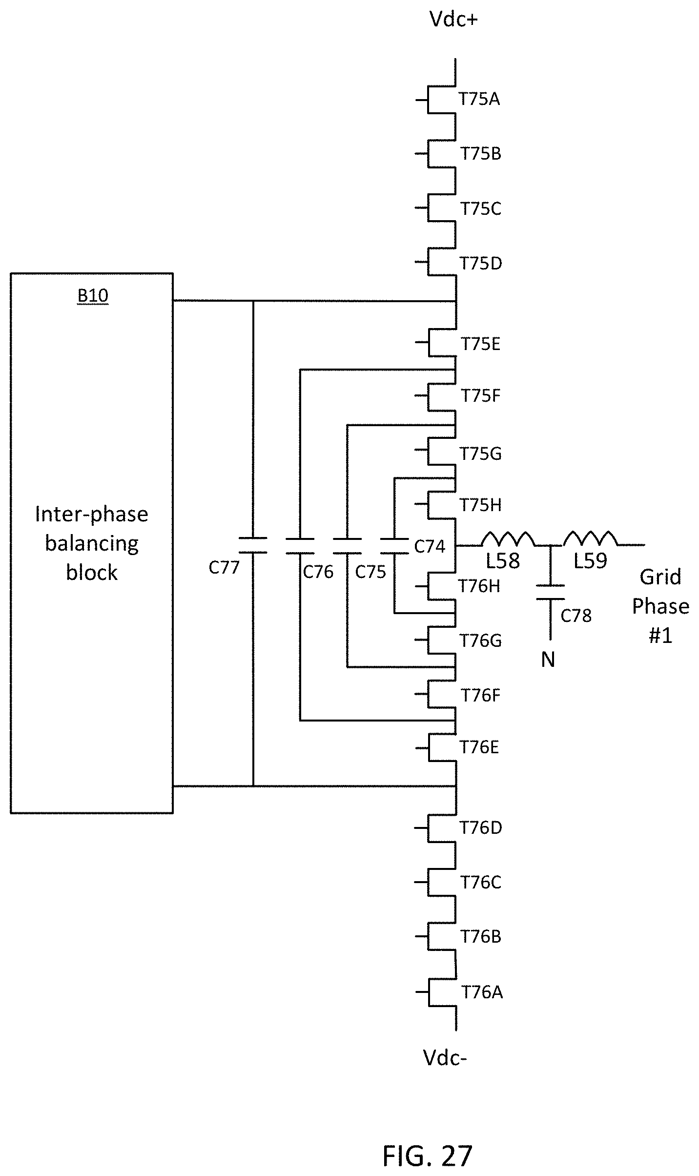
D00033
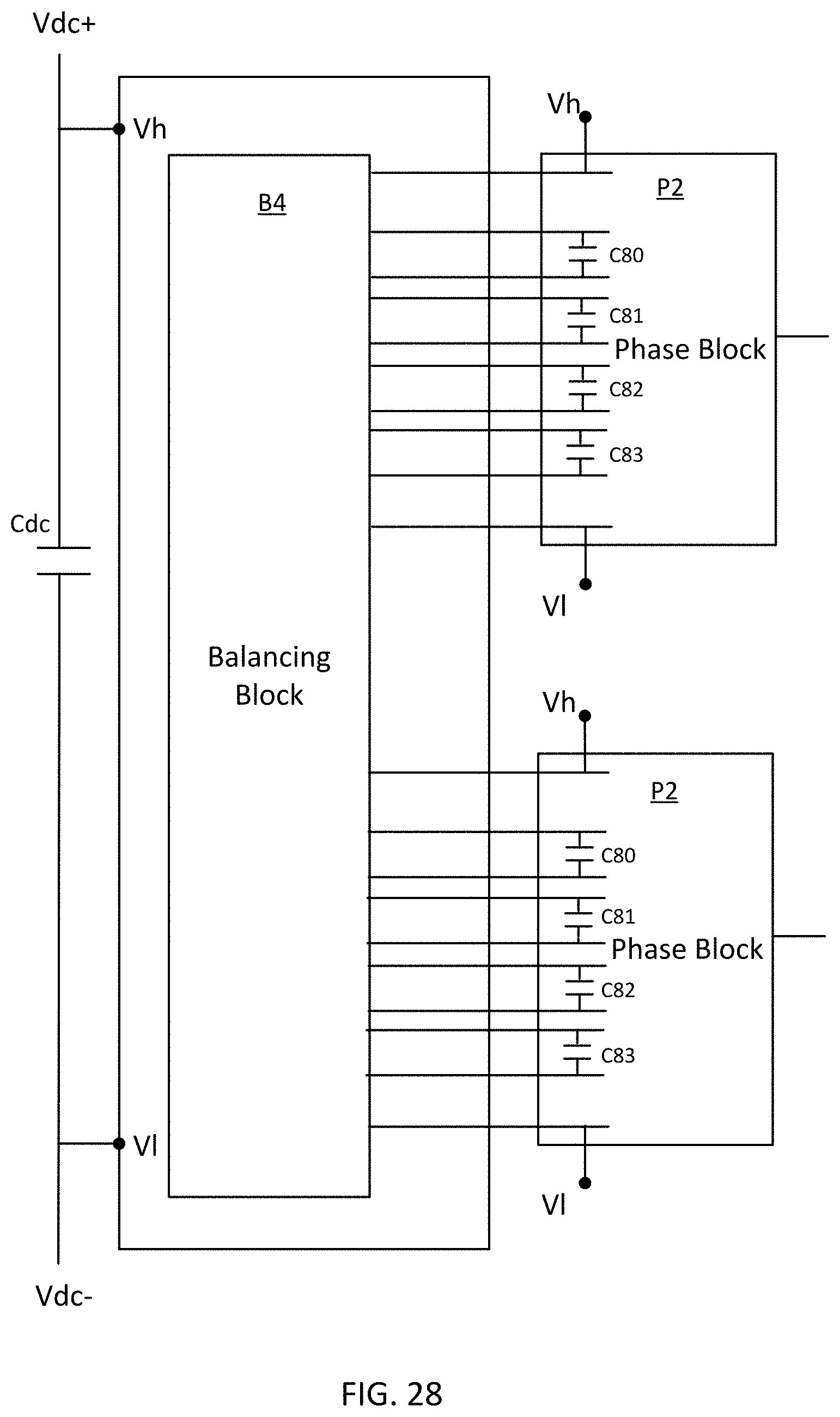
D00034
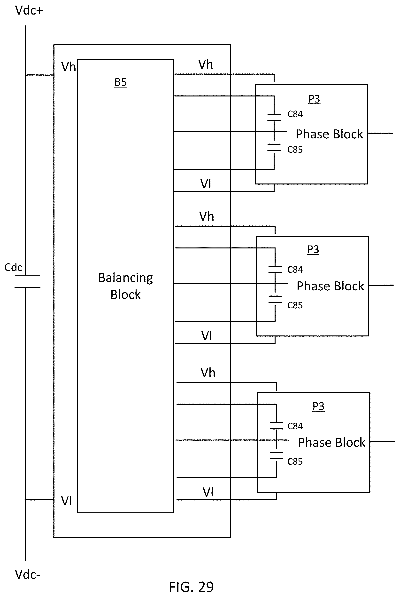
D00035
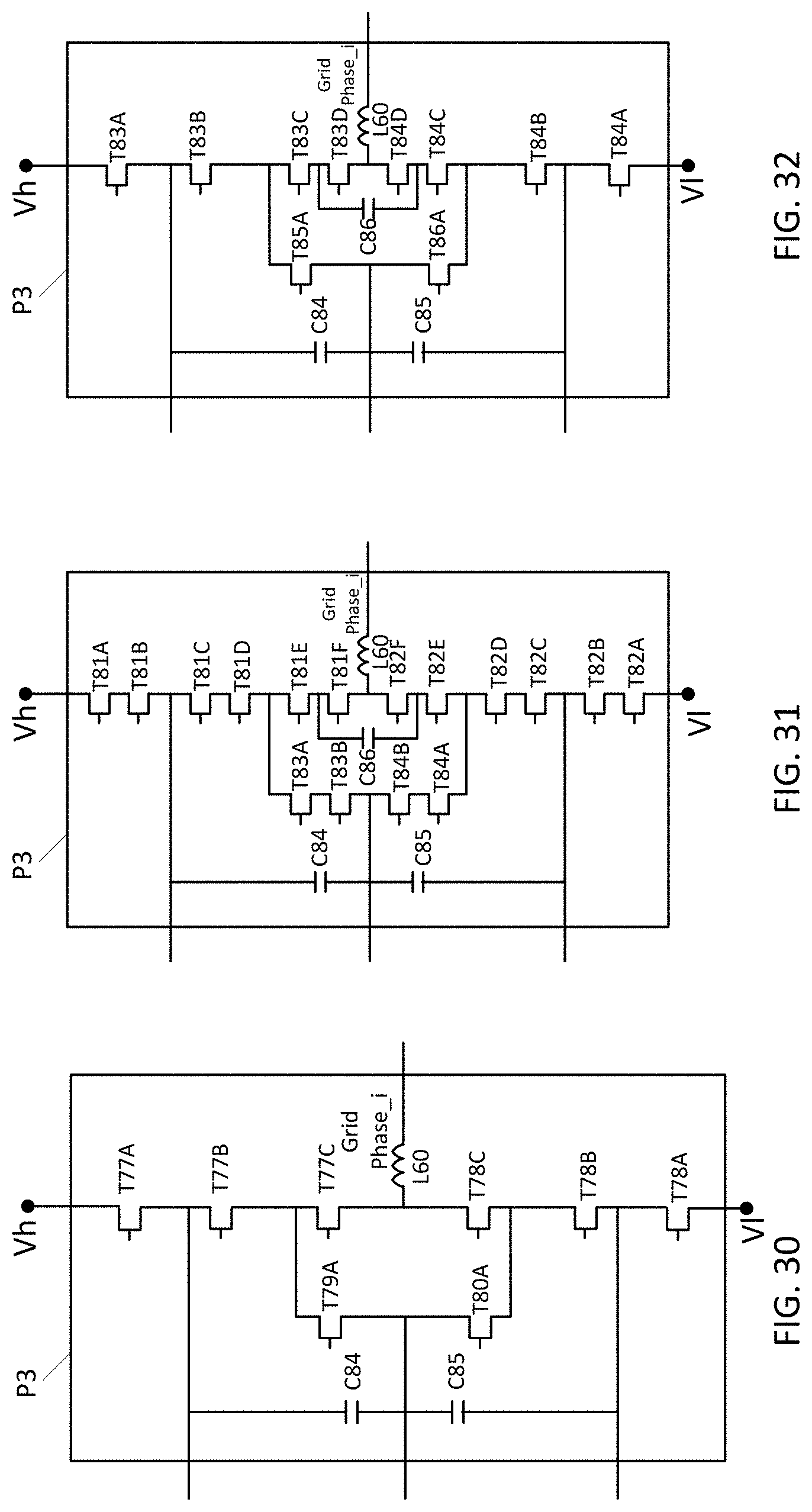
D00036
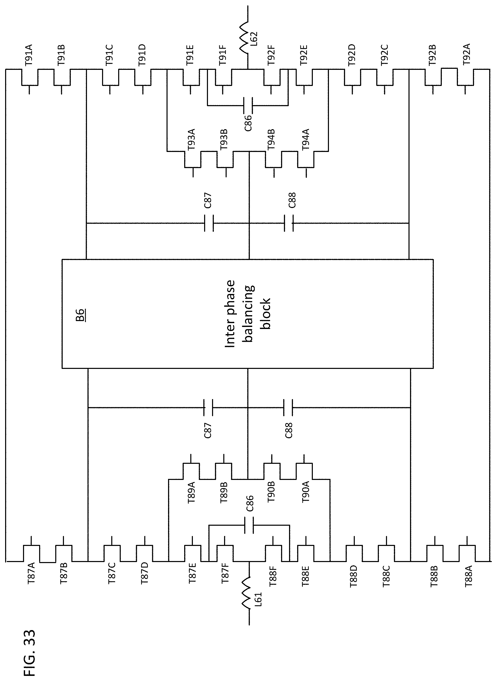
D00037
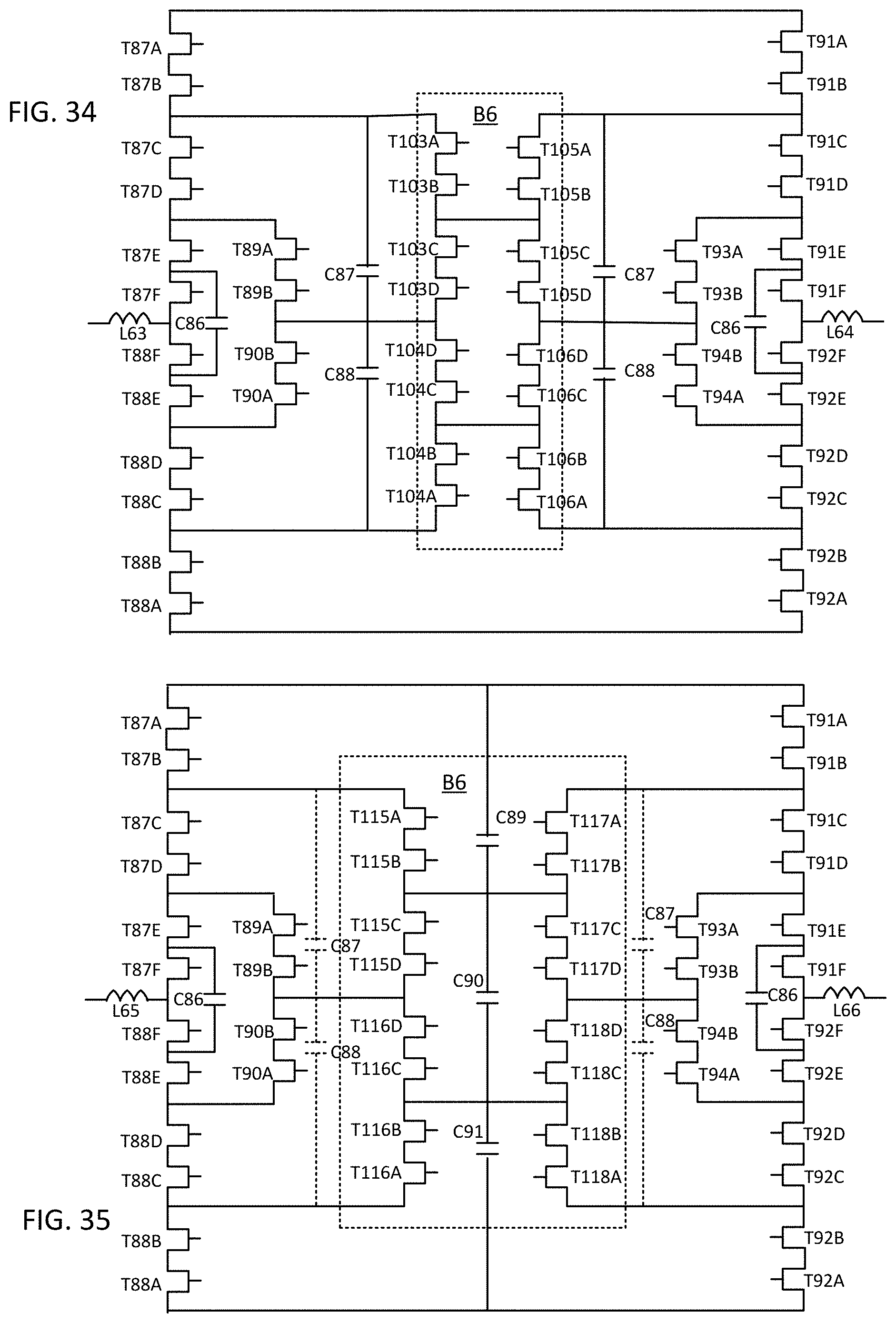
D00038
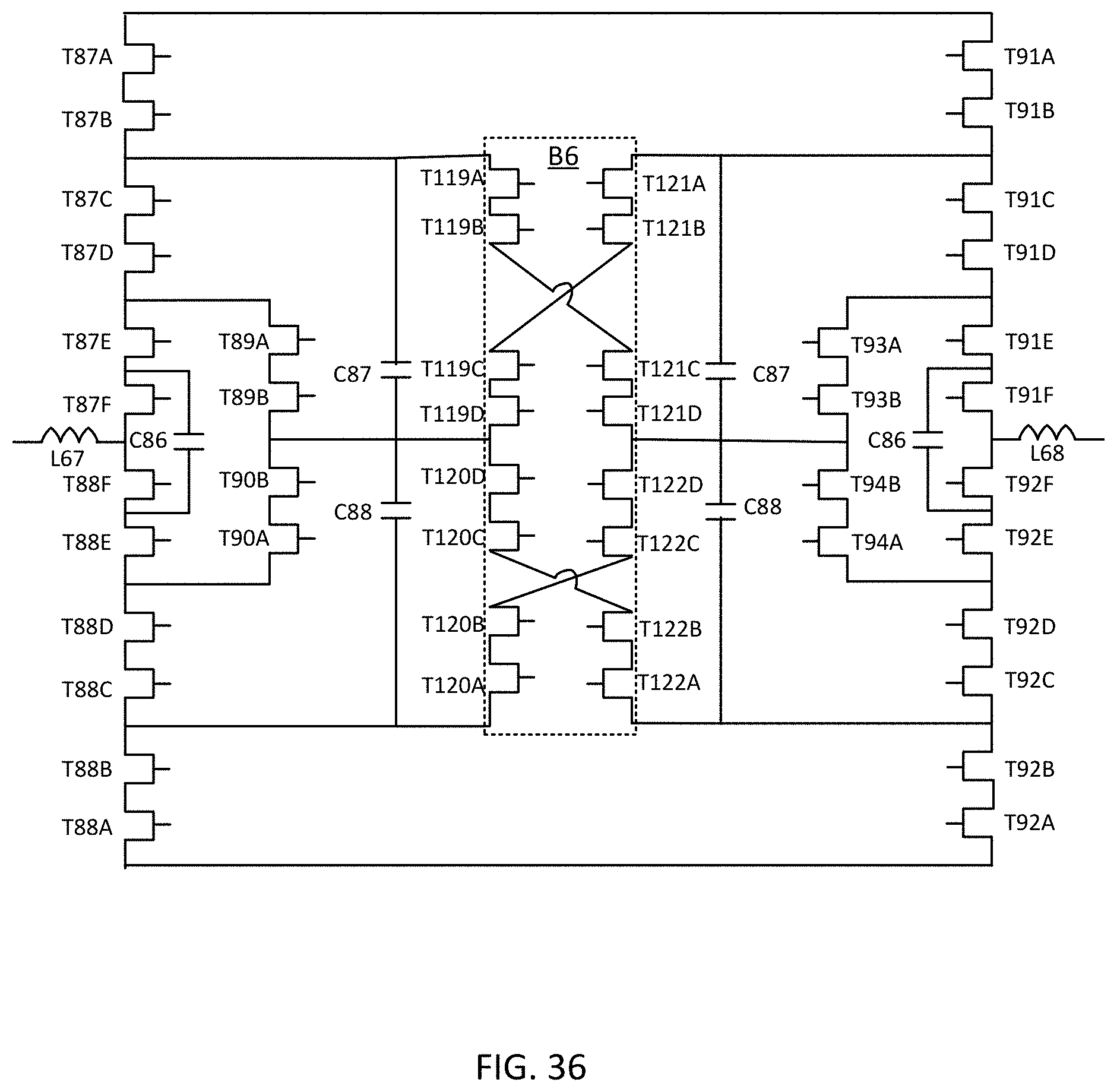
D00039

D00040

D00041
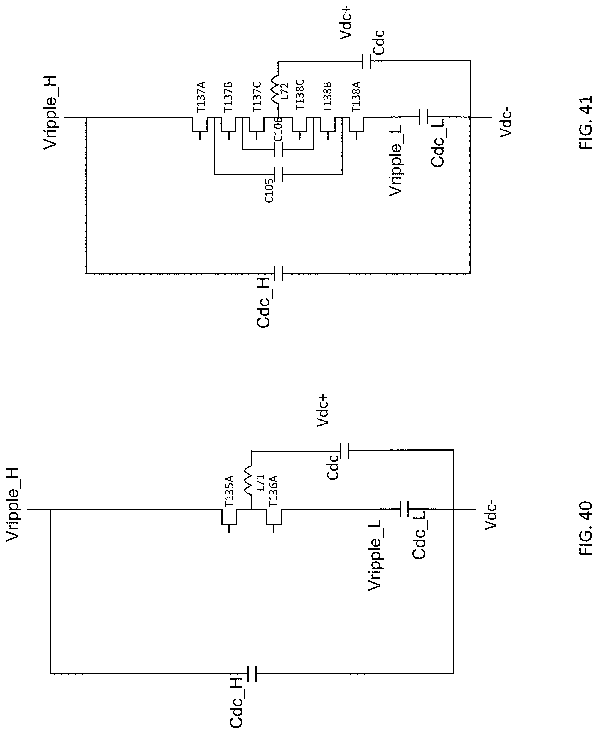
D00042

D00043
D00044
D00045
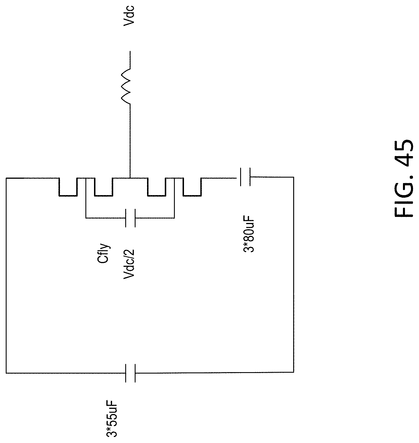
D00046
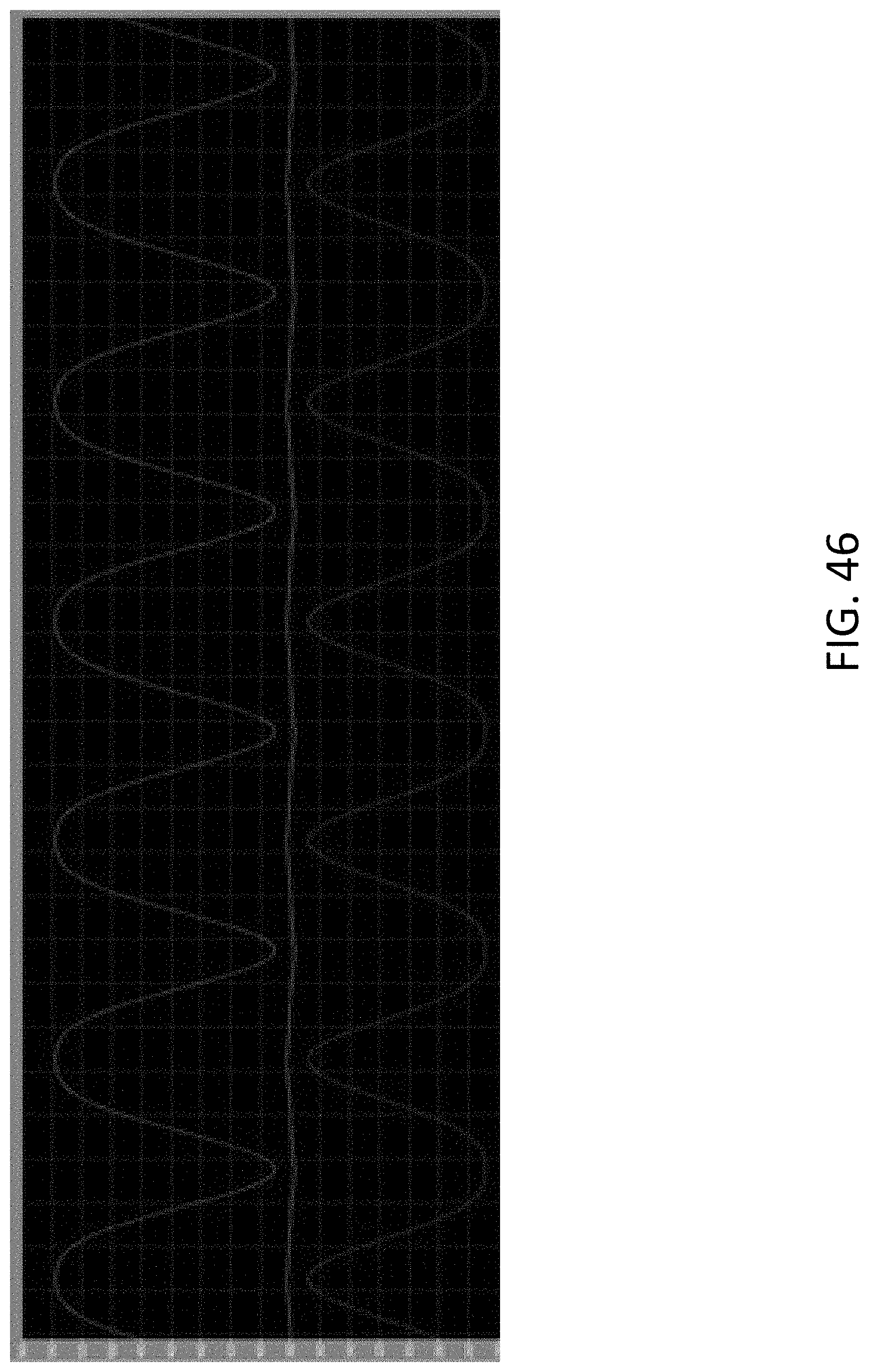
XML
uspto.report is an independent third-party trademark research tool that is not affiliated, endorsed, or sponsored by the United States Patent and Trademark Office (USPTO) or any other governmental organization. The information provided by uspto.report is based on publicly available data at the time of writing and is intended for informational purposes only.
While we strive to provide accurate and up-to-date information, we do not guarantee the accuracy, completeness, reliability, or suitability of the information displayed on this site. The use of this site is at your own risk. Any reliance you place on such information is therefore strictly at your own risk.
All official trademark data, including owner information, should be verified by visiting the official USPTO website at www.uspto.gov. This site is not intended to replace professional legal advice and should not be used as a substitute for consulting with a legal professional who is knowledgeable about trademark law.