Pixels and reference circuits and timing techniques
Chaji , et al.
U.S. patent number 10,657,895 [Application Number 15/797,661] was granted by the patent office on 2020-05-19 for pixels and reference circuits and timing techniques. This patent grant is currently assigned to Ignis Innovation Inc.. The grantee listed for this patent is Ignis Innovation Inc.. Invention is credited to Yaser Azizi, Gholamreza Chaji, Hongxin Liu, Arash Moradi.


View All Diagrams
| United States Patent | 10,657,895 |
| Chaji , et al. | May 19, 2020 |
Pixels and reference circuits and timing techniques
Abstract
What is disclosed are systems and methods of compensation of images produced by active matrix light emitting diode device (AMOLED) and other emissive displays. Anomalies in luminance produced by pixel circuits and bias currents produced by current biasing circuits for driving current biased voltage programmed pixels are corrected through calibration and compensation while re-using existing data or other lines that can be controlled individually to perform said calibration and compensation.
| Inventors: | Chaji; Gholamreza (Waterloo, CA), Azizi; Yaser (Waterloo, CA), Moradi; Arash (Waterloo, CA), Liu; Hongxin (Cambridge, CA) | ||||||||||
|---|---|---|---|---|---|---|---|---|---|---|---|
| Applicant: |
|
||||||||||
| Assignee: | Ignis Innovation Inc.
(Waterloo, CA) |
||||||||||
| Family ID: | 61280724 | ||||||||||
| Appl. No.: | 15/797,661 | ||||||||||
| Filed: | October 30, 2017 |
Prior Publication Data
| Document Identifier | Publication Date | |
|---|---|---|
| US 20180068611 A1 | Mar 8, 2018 | |
Related U.S. Patent Documents
| Application Number | Filing Date | Patent Number | Issue Date | ||
|---|---|---|---|---|---|
| 15361660 | Nov 28, 2016 | 10373554 | |||
| 15215036 | Jul 20, 2016 | 10410579 | |||
Foreign Application Priority Data
| Jul 24, 2015 [CA] | 2898282 | |||
| Current U.S. Class: | 1/1 |
| Current CPC Class: | G09G 3/325 (20130101); G09G 3/3233 (20130101); G09G 3/006 (20130101); G09G 2310/061 (20130101); G09G 2310/0297 (20130101); G09G 2330/10 (20130101); G09G 2320/0693 (20130101); G09G 2320/0233 (20130101); G09G 2300/0819 (20130101); G09G 2320/045 (20130101); G09G 2320/0295 (20130101); G09G 2310/08 (20130101); G09G 2330/12 (20130101) |
| Current International Class: | G09G 3/325 (20160101); G09G 3/3233 (20160101) |
References Cited [Referenced By]
U.S. Patent Documents
| 3506851 | April 1970 | Polkinghorn et al. |
| 3750987 | August 1973 | Gobel |
| 3774055 | November 1973 | Bapat et al. |
| 4090096 | May 1978 | Nagami |
| 4354162 | October 1982 | Wright |
| 4758831 | July 1988 | Kasahara et al. |
| 4963860 | October 1990 | Stewart |
| 4975691 | December 1990 | Lee |
| 4996523 | February 1991 | Bell et al. |
| 5051739 | September 1991 | Hayashida et al. |
| 5134387 | July 1992 | Smith et al. |
| 5153420 | October 1992 | Hack et al. |
| 5170158 | December 1992 | Shinya |
| 5204661 | April 1993 | Hack et al. |
| 5222082 | June 1993 | Plus |
| 5266515 | November 1993 | Robb et al. |
| 5278542 | January 1994 | Smith et al. |
| 5408267 | April 1995 | Main |
| 5498880 | March 1996 | Lee et al. |
| 5572444 | November 1996 | Lentz et al. |
| 5589847 | December 1996 | Lewis |
| 5619033 | April 1997 | Weisfield |
| 5648276 | July 1997 | Hara et al. |
| 5670973 | September 1997 | Bassetti et al. |
| 5684365 | November 1997 | Tang et al. |
| 5686935 | November 1997 | Weisbrod |
| 5691783 | November 1997 | Numao et al. |
| 5701505 | December 1997 | Yamashita et al. |
| 5712653 | January 1998 | Katoh et al. |
| 5714968 | February 1998 | Ikeda |
| 5744824 | April 1998 | Kousai et al. |
| 5745660 | April 1998 | Kolpatzik et al. |
| 5747928 | May 1998 | Shanks et al. |
| 5748160 | May 1998 | Shieh et al. |
| 5758129 | May 1998 | Gray et al. |
| 5784042 | July 1998 | Ono et al. |
| 5790234 | August 1998 | Matsuyama |
| 5815303 | September 1998 | Berlin |
| 5835376 | November 1998 | Smith et al. |
| 5870071 | February 1999 | Kawahata |
| 5874803 | February 1999 | Garbuzov et al. |
| 5880582 | March 1999 | Sawada |
| 5903248 | May 1999 | Irwin |
| 5917280 | June 1999 | Burrows et al. |
| 5923794 | July 1999 | McGrath et al. |
| 5949398 | September 1999 | Kim |
| 5952789 | September 1999 | Stewart et al. |
| 5990629 | November 1999 | Yamada et al. |
| 6023259 | February 2000 | Howard et al. |
| 6069365 | May 2000 | Chow et al. |
| 6081131 | June 2000 | Ishii |
| 6091203 | July 2000 | Kawashima et al. |
| 6097360 | August 2000 | Holloman |
| 6100868 | August 2000 | Lee et al. |
| 6144222 | November 2000 | Ho |
| 6157583 | December 2000 | Starnes et al. |
| 6166489 | December 2000 | Thompson et al. |
| 6177915 | January 2001 | Beeteson et al. |
| 6225846 | May 2001 | Wada et al. |
| 6229506 | May 2001 | Dawson et al. |
| 6229508 | May 2001 | Kane |
| 6232939 | May 2001 | Saito et al. |
| 6246180 | June 2001 | Nishigaki |
| 6252248 | June 2001 | Sano et al. |
| 6259424 | July 2001 | Kurogane |
| 6268841 | July 2001 | Cairns et al. |
| 6274887 | August 2001 | Yamazaki et al. |
| 6288696 | September 2001 | Holloman |
| 6300928 | October 2001 | Kim |
| 6303963 | October 2001 | Ohtani et al. |
| 6306694 | October 2001 | Yamazaki et al. |
| 6307322 | October 2001 | Dawson et al. |
| 6310962 | October 2001 | Chung et al. |
| 6316786 | November 2001 | Mueller et al. |
| 6320325 | November 2001 | Cok et al. |
| 6323631 | November 2001 | Juang |
| 6323832 | November 2001 | Nishizawa et al. |
| 6333729 | December 2001 | Ha |
| 6345085 | February 2002 | Yeo et al. |
| 6348835 | February 2002 | Sato et al. |
| 6365917 | April 2002 | Yamazaki |
| 6373453 | April 2002 | Yudasaka |
| 6384427 | May 2002 | Yamazaki et al. |
| 6384804 | May 2002 | Dodabalapur et al. |
| 6388653 | May 2002 | Goto et al. |
| 6392617 | May 2002 | Gleason |
| 6396469 | May 2002 | Miwa et al. |
| 6399988 | June 2002 | Yamazaki |
| 6414661 | July 2002 | Shen et al. |
| 6417825 | July 2002 | Stewart et al. |
| 6420758 | July 2002 | Nakajima |
| 6420834 | July 2002 | Yamazaki et al. |
| 6420988 | July 2002 | Azami et al. |
| 6430496 | August 2002 | Smith et al. |
| 6433488 | August 2002 | Bu |
| 6445376 | September 2002 | Parrish |
| 6468638 | October 2002 | Jacobsen et al. |
| 6473065 | October 2002 | Fan |
| 6475845 | November 2002 | Kimura |
| 6489952 | December 2002 | Tanaka et al. |
| 6501098 | December 2002 | Yamazaki |
| 6501466 | December 2002 | Yamagashi et al. |
| 6512271 | January 2003 | Yamazaki et al. |
| 6518594 | February 2003 | Nakajima et al. |
| 6522315 | February 2003 | Ozawa et al. |
| 6524895 | February 2003 | Yamazaki et al. |
| 6531713 | March 2003 | Yamazaki |
| 6535185 | March 2003 | Kim et al. |
| 6542138 | April 2003 | Shannon et al. |
| 6559594 | May 2003 | Fukunaga et al. |
| 6559839 | May 2003 | Ueno et al. |
| 6573195 | June 2003 | Yamazaki et al. |
| 6573584 | June 2003 | Nagakari et al. |
| 6576926 | June 2003 | Yamazaki et al. |
| 6577302 | June 2003 | Hunter |
| 6580408 | June 2003 | Bae et al. |
| 6580657 | June 2003 | Sanford et al. |
| 6583398 | June 2003 | Harkin |
| 6583775 | June 2003 | Sekiya et al. |
| 6583776 | June 2003 | Yamazaki et al. |
| 6587086 | July 2003 | Koyama |
| 6593691 | July 2003 | Nishi et al. |
| 6594606 | July 2003 | Everitt |
| 6597203 | July 2003 | Forbes |
| 6611108 | August 2003 | Kimura |
| 6617644 | September 2003 | Yamazaki et al. |
| 6618030 | September 2003 | Kane et al. |
| 6639244 | October 2003 | Yamazaki et al. |
| 6641933 | November 2003 | Yamazaki et al. |
| 6661180 | December 2003 | Koyama |
| 6661397 | December 2003 | Mikami et al. |
| 6670637 | December 2003 | Yamazaki et al. |
| 6677713 | January 2004 | Sung |
| 6680577 | January 2004 | Inukai et al. |
| 6680580 | January 2004 | Sung |
| 6686699 | February 2004 | Yumoto |
| 6687266 | February 2004 | Ma et al. |
| 6690000 | February 2004 | Muramatsu et al. |
| 6690344 | February 2004 | Takeuchi et al. |
| 6693388 | February 2004 | Oomura |
| 6693610 | February 2004 | Shannon et al. |
| 6694248 | February 2004 | Smith et al. |
| 6697057 | February 2004 | Koyama et al. |
| 6720942 | April 2004 | Lee et al. |
| 6724151 | April 2004 | Yoo |
| 6734636 | May 2004 | Sanford et al. |
| 6738034 | May 2004 | Kaneko et al. |
| 6738035 | May 2004 | Fan |
| 6753655 | June 2004 | Shih et al. |
| 6753834 | June 2004 | Mikami et al. |
| 6756741 | June 2004 | Li |
| 6756958 | June 2004 | Furuhashi et al. |
| 6771028 | August 2004 | Winters |
| 6777712 | August 2004 | Sanford et al. |
| 6777888 | August 2004 | Kondo |
| 6780687 | August 2004 | Nakajima et al. |
| 6781567 | August 2004 | Kimura |
| 6788231 | September 2004 | Hsueh |
| 6806638 | October 2004 | Lih et al. |
| 6806857 | October 2004 | Sempel et al. |
| 6809706 | October 2004 | Shimoda |
| 6828950 | December 2004 | Koyama |
| 6858991 | February 2005 | Miyazawa |
| 6859193 | February 2005 | Yumoto |
| 6861670 | March 2005 | Ohtani et al. |
| 6873117 | March 2005 | Ishizuka |
| 6873320 | March 2005 | Nakamura |
| 6876346 | April 2005 | Anzai et al. |
| 6878968 | April 2005 | Ohnuma |
| 6900485 | May 2005 | Lee |
| 6903734 | June 2005 | Eu |
| 6909114 | June 2005 | Yamazaki |
| 6909419 | June 2005 | Zavracky et al. |
| 6911960 | June 2005 | Yokoyama |
| 6911964 | June 2005 | Lee et al. |
| 6914448 | July 2005 | Jinno |
| 6919871 | July 2005 | Kwon |
| 6924602 | August 2005 | Komiya |
| 6937215 | August 2005 | Lo |
| 6937220 | August 2005 | Kitaura et al. |
| 6940214 | September 2005 | Komiya et al. |
| 6943500 | September 2005 | LeChevalier |
| 6954194 | October 2005 | Matsumoto et al. |
| 6956547 | October 2005 | Bae et al. |
| 6970149 | November 2005 | Chung et al. |
| 6975142 | December 2005 | Azami et al. |
| 6975332 | December 2005 | Arnold et al. |
| 6995510 | February 2006 | Murakami et al. |
| 6995519 | February 2006 | Arnold et al. |
| 7022556 | April 2006 | Adachi |
| 7023408 | April 2006 | Chen et al. |
| 7027015 | April 2006 | Booth, Jr. et al. |
| 7034793 | April 2006 | Sekiya et al. |
| 7038392 | May 2006 | Libsch et al. |
| 7057588 | June 2006 | Asano et al. |
| 7061451 | June 2006 | Kimura |
| 7071932 | July 2006 | Libsch et al. |
| 7088051 | August 2006 | Cok |
| 7106285 | September 2006 | Naugler |
| 7112820 | September 2006 | Chang et al. |
| 7113864 | September 2006 | Smith et al. |
| 7116058 | October 2006 | Lo et al. |
| 7122835 | October 2006 | Ikeda et al. |
| 7129914 | October 2006 | Knapp et al. |
| 7129917 | October 2006 | Yamazaki et al. |
| 7141821 | November 2006 | Yamazaki et al. |
| 7161566 | January 2007 | Cok et al. |
| 7164417 | January 2007 | Cok |
| 7193589 | March 2007 | Yoshida et al. |
| 7199516 | April 2007 | Seo et al. |
| 7220997 | May 2007 | Nakata |
| 7224332 | May 2007 | Cok |
| 7235810 | June 2007 | Yamazaki et al. |
| 7245277 | July 2007 | Ishizuka |
| 7248236 | July 2007 | Nathan et al. |
| 7259737 | August 2007 | Ono et al. |
| 7262753 | August 2007 | Tanghe et al. |
| 7264979 | September 2007 | Yamagata et al. |
| 7274345 | September 2007 | Imamura et al. |
| 7274363 | September 2007 | Ishizuka et al. |
| 7279711 | October 2007 | Yamazaki et al. |
| 7304621 | December 2007 | Oomori et al. |
| 7310092 | December 2007 | Imamura |
| 7315295 | January 2008 | Kimura |
| 7317429 | January 2008 | Shirasaki et al. |
| 7317434 | January 2008 | Lan et al. |
| 7319465 | January 2008 | Mikami et al. |
| 7321348 | January 2008 | Cok et al. |
| 7327357 | February 2008 | Jeong |
| 7333077 | February 2008 | Koyama et al. |
| 7339636 | March 2008 | Voloschenko et al. |
| 7343243 | March 2008 | Smith et al. |
| 7355574 | April 2008 | Leon et al. |
| 7358941 | April 2008 | Ono et al. |
| 7402467 | July 2008 | Kadono et al. |
| 7414600 | August 2008 | Nathan et al. |
| 7432885 | October 2008 | Asano et al. |
| 7466166 | December 2008 | Date et al. |
| 7474285 | January 2009 | Kimura |
| 7485478 | February 2009 | Yamagata et al. |
| 7495501 | February 2009 | Iwabuchi et al. |
| 7502000 | March 2009 | Yuki et al. |
| 7515124 | April 2009 | Yaguma et al. |
| 7535449 | May 2009 | Miyazawa |
| 7554512 | June 2009 | Steer |
| 7569849 | August 2009 | Nathan et al. |
| 7595776 | September 2009 | Hashimoto et al. |
| 7604718 | October 2009 | Zhang et al. |
| 7609239 | October 2009 | Chang |
| 7612745 | November 2009 | Yumoto et al. |
| 7619594 | November 2009 | Hu |
| 7619597 | November 2009 | Nathan et al. |
| 7639211 | December 2009 | Miyazawa |
| 7683899 | March 2010 | Hirakata et al. |
| 7688289 | March 2010 | Abe et al. |
| 7697052 | April 2010 | Yamazaki et al. |
| 7760162 | July 2010 | Miyazawa |
| 7808008 | October 2010 | Miyake |
| 7825419 | November 2010 | Yamagata et al. |
| 7859492 | December 2010 | Kohno |
| 7859520 | December 2010 | Kimura |
| 7868859 | January 2011 | Tomida et al. |
| 7876294 | January 2011 | Sasaki et al. |
| 7889159 | February 2011 | Nathan et al. |
| 7903127 | March 2011 | Kwon |
| 7920116 | April 2011 | Woo et al. |
| 7944414 | May 2011 | Shirasaki et al. |
| 7948170 | May 2011 | Striakhilev et al. |
| 7969390 | June 2011 | Yoshida |
| 7978170 | July 2011 | Park et al. |
| 7989392 | August 2011 | Crockett et al. |
| 7995008 | August 2011 | Miwa |
| 7995010 | August 2011 | Yamazaki et al. |
| 8044893 | October 2011 | Nathan et al. |
| 8063852 | November 2011 | Kwak et al. |
| 8102343 | January 2012 | Yatabe |
| 8115707 | February 2012 | Nathan et al. |
| 8144081 | March 2012 | Miyazawa |
| 8159007 | April 2012 | Bama et al. |
| 8242979 | August 2012 | Anzai et al. |
| 8253665 | August 2012 | Nathan et al. |
| 8283967 | October 2012 | Chaji et al. |
| 8319712 | November 2012 | Nathan et al. |
| 8378362 | February 2013 | Heo et al. |
| 8493295 | July 2013 | Yamazaki et al. |
| 8497525 | July 2013 | Yamagata et al. |
| 8564513 | October 2013 | Nathan et al. |
| 8872739 | October 2014 | Kimura |
| 2001/0002703 | June 2001 | Koyama |
| 2001/0004190 | June 2001 | Nishi et al. |
| 2001/0009283 | July 2001 | Arao et al. |
| 2001/0013806 | August 2001 | Notani |
| 2001/0015653 | August 2001 | De Jong et al. |
| 2001/0020926 | September 2001 | Kujik |
| 2001/0024186 | September 2001 | Kane et al. |
| 2001/0026127 | October 2001 | Yoneda et al. |
| 2001/0026179 | October 2001 | Saeki |
| 2001/0026257 | October 2001 | Kimura |
| 2001/0030323 | October 2001 | Ikeda |
| 2001/0033199 | October 2001 | Aoki |
| 2001/0035863 | November 2001 | Kimura |
| 2001/0038098 | November 2001 | Yamazaki et al. |
| 2001/0040541 | November 2001 | Yoneda et al. |
| 2001/0043173 | November 2001 | Troutman |
| 2001/0045929 | November 2001 | Prache et al. |
| 2001/0052606 | December 2001 | Sempel et al. |
| 2001/0052898 | December 2001 | Osame et al. |
| 2001/0052940 | December 2001 | Hagihara et al. |
| 2002/0000576 | January 2002 | Inukai |
| 2002/0011796 | January 2002 | Koyama |
| 2002/0011799 | January 2002 | Kimura |
| 2002/0011981 | January 2002 | Kujik |
| 2002/0012057 | January 2002 | Kimura |
| 2002/0015031 | February 2002 | Fujita et al. |
| 2002/0015032 | February 2002 | Koyama et al. |
| 2002/0030190 | March 2002 | Ohtani et al. |
| 2002/0030528 | March 2002 | Matsumoto et al. |
| 2002/0030647 | March 2002 | Hack et al. |
| 2002/0036463 | March 2002 | Yoneda et al. |
| 2002/0047565 | April 2002 | Nara et al. |
| 2002/0047852 | April 2002 | Inukai et al. |
| 2002/0048829 | April 2002 | Yamazaki et al. |
| 2002/0050795 | May 2002 | Imura |
| 2002/0052086 | May 2002 | Maeda |
| 2002/0053401 | May 2002 | Ishikawa et al. |
| 2002/0070909 | June 2002 | Asano et al. |
| 2002/0080108 | June 2002 | Wang |
| 2002/0084463 | July 2002 | Sanford et al. |
| 2002/0101172 | August 2002 | Bu |
| 2002/0101433 | August 2002 | McKnight |
| 2002/0113248 | August 2002 | Yamagata et al. |
| 2002/0117722 | August 2002 | Osada et al. |
| 2002/0122308 | September 2002 | Ikeda |
| 2002/0130686 | September 2002 | Forbes |
| 2002/0140712 | October 2002 | Ouchi et al. |
| 2002/0154084 | October 2002 | Tanaka et al. |
| 2002/0158587 | October 2002 | Komiya |
| 2002/0158666 | October 2002 | Azami et al. |
| 2002/0158823 | October 2002 | Zavracky et al. |
| 2002/0163314 | November 2002 | Yamazaki et al. |
| 2002/0167471 | November 2002 | Everitt |
| 2002/0171613 | November 2002 | Goto et al. |
| 2002/0180369 | December 2002 | Koyama |
| 2002/0180721 | December 2002 | Kimura et al. |
| 2002/0181275 | December 2002 | Yamazaki |
| 2002/0186214 | December 2002 | Siwinski |
| 2002/0190332 | December 2002 | Lee et al. |
| 2002/0190924 | December 2002 | Asano et al. |
| 2002/0190971 | December 2002 | Nakamura et al. |
| 2002/0195967 | December 2002 | Kim et al. |
| 2002/0195968 | December 2002 | Sanford et al. |
| 2002/0196213 | December 2002 | Akimoto et al. |
| 2003/0001828 | January 2003 | Asano |
| 2003/0001858 | January 2003 | Jack |
| 2003/0016190 | January 2003 | Kondo |
| 2003/0020413 | January 2003 | Oomura |
| 2003/0030603 | February 2003 | Shimoda |
| 2003/0062524 | April 2003 | Kimura |
| 2003/0062844 | April 2003 | Miyazawa |
| 2003/0063081 | April 2003 | Kimura et al. |
| 2003/0071804 | April 2003 | Yamazaki et al. |
| 2003/0071821 | April 2003 | Sundahl |
| 2003/0076048 | April 2003 | Rutherford |
| 2003/0090445 | May 2003 | Chen et al. |
| 2003/0090447 | May 2003 | Kimura |
| 2003/0090481 | May 2003 | Kimura |
| 2003/0095087 | May 2003 | Libsch |
| 2003/0098829 | May 2003 | Chen et al. |
| 2003/0107560 | June 2003 | Yumoto et al. |
| 2003/0107561 | June 2003 | Uchino et al. |
| 2003/0111966 | June 2003 | Mikami et al. |
| 2003/0112205 | June 2003 | Yamada |
| 2003/0112208 | June 2003 | Okabe et al. |
| 2003/0117348 | June 2003 | Knapp et al. |
| 2003/0122474 | July 2003 | Lee |
| 2003/0122745 | July 2003 | Miyazawa |
| 2003/0122747 | July 2003 | Shannon et al. |
| 2003/0128199 | July 2003 | Kimura |
| 2003/0140958 | July 2003 | Yang et al. |
| 2003/0151569 | August 2003 | Lee et al. |
| 2003/0156104 | August 2003 | Morita |
| 2003/0169219 | September 2003 | LeChevalier |
| 2003/0169241 | September 2003 | LeChevalier |
| 2003/0169247 | September 2003 | Kawabe et al. |
| 2003/0174152 | September 2003 | Noguchi |
| 2003/0178617 | September 2003 | Appenzeller et al. |
| 2003/0179626 | September 2003 | Sanford et al. |
| 2003/0185438 | October 2003 | Osawa et al. |
| 2003/0189535 | October 2003 | Matsumoto et al. |
| 2003/0197663 | October 2003 | Lee et al. |
| 2003/0206060 | November 2003 | Suzuki |
| 2003/0214465 | November 2003 | Kimura |
| 2003/0227262 | December 2003 | Kwon |
| 2003/0230141 | December 2003 | Gilmour et al. |
| 2003/0230980 | December 2003 | Forrest et al. |
| 2004/0004589 | January 2004 | Shih |
| 2004/0027063 | February 2004 | Nishikawa |
| 2004/0032382 | February 2004 | Cok et al. |
| 2004/0041750 | March 2004 | Abe |
| 2004/0056604 | March 2004 | Shih et al. |
| 2004/0066357 | April 2004 | Kawasaki |
| 2004/0070557 | April 2004 | Asano et al. |
| 2004/0070558 | April 2004 | Cok |
| 2004/0080262 | April 2004 | Park et al. |
| 2004/0080470 | April 2004 | Yamazaki et al. |
| 2004/0090186 | May 2004 | Yoshida et al. |
| 2004/0090400 | May 2004 | Yoo |
| 2004/0095338 | May 2004 | Takashi |
| 2004/0108518 | June 2004 | Jo |
| 2004/0113903 | June 2004 | Mikami et al. |
| 2004/0129933 | July 2004 | Nathan et al. |
| 2004/0130516 | July 2004 | Nathan et al. |
| 2004/0135749 | July 2004 | Kondakov et al. |
| 2004/0145547 | July 2004 | Oh |
| 2004/0150592 | August 2004 | Mizukoshi et al. |
| 2004/0150594 | August 2004 | Koyama et al. |
| 2004/0150595 | August 2004 | Kasai |
| 2004/0155841 | August 2004 | Kasai |
| 2004/0171619 | September 2004 | Barkoczy et al. |
| 2004/0174347 | September 2004 | Sun et al. |
| 2004/0174349 | September 2004 | Libsch |
| 2004/0174354 | September 2004 | Ono |
| 2004/0183759 | September 2004 | Stevenson et al. |
| 2004/0189627 | September 2004 | Shirasaki et al. |
| 2004/0196275 | October 2004 | Hattori |
| 2004/0201554 | October 2004 | Satoh |
| 2004/0207615 | October 2004 | Yumoto |
| 2004/0227697 | November 2004 | Mori |
| 2004/0233125 | November 2004 | Tanghe et al. |
| 2004/0239596 | December 2004 | Ono et al. |
| 2004/0239696 | December 2004 | Okabe |
| 2004/0251844 | December 2004 | Hashido et al. |
| 2004/0252085 | December 2004 | Miyagawa |
| 2004/0252089 | December 2004 | Ono et al. |
| 2004/0256617 | December 2004 | Yamada et al. |
| 2004/0257353 | December 2004 | Imamura et al. |
| 2004/0257355 | December 2004 | Naugler |
| 2004/0263437 | December 2004 | Hattori |
| 2005/0007357 | January 2005 | Yamashita et al. |
| 2005/0030267 | February 2005 | Tanghe et al. |
| 2005/0035709 | February 2005 | Furuie et al. |
| 2005/0052379 | March 2005 | Waterman |
| 2005/0057459 | March 2005 | Miyazawa |
| 2005/0067970 | March 2005 | Libsch et al. |
| 2005/0067971 | March 2005 | Kane |
| 2005/0068270 | March 2005 | Awakura |
| 2005/0083270 | April 2005 | Miyazawa |
| 2005/0088085 | April 2005 | Nishikawa et al. |
| 2005/0088103 | April 2005 | Kageyama et al. |
| 2005/0110420 | May 2005 | Arnold et al. |
| 2005/0110727 | May 2005 | Shin |
| 2005/0117096 | June 2005 | Voloschenko et al. |
| 2005/0123193 | June 2005 | Lamberg et al. |
| 2005/0140598 | June 2005 | Kim et al. |
| 2005/0140600 | June 2005 | Kim et al. |
| 2005/0140610 | June 2005 | Smith et al. |
| 2005/0145891 | July 2005 | Abe |
| 2005/0156831 | July 2005 | Yamazaki et al. |
| 2005/0168416 | August 2005 | Hashimoto et al. |
| 2005/0206590 | September 2005 | Sasaki et al. |
| 2005/0212787 | September 2005 | Noguchi et al. |
| 2005/0219188 | October 2005 | Kawabe et al. |
| 2005/0225686 | October 2005 | Brummack et al. |
| 2005/0243037 | November 2005 | Eom et al. |
| 2005/0248515 | November 2005 | Naugler et al. |
| 2005/0258867 | November 2005 | Miyazawa |
| 2005/0260777 | November 2005 | Brabec et al. |
| 2005/0269959 | December 2005 | Uchino et al. |
| 2005/0269960 | December 2005 | Ono et al. |
| 2005/0285822 | December 2005 | Reddy et al. |
| 2005/0285825 | December 2005 | Eom et al. |
| 2006/0007072 | January 2006 | Choi et al. |
| 2006/0012310 | January 2006 | Chen et al. |
| 2006/0012311 | January 2006 | Ogawa |
| 2006/0022305 | February 2006 | Yamashita |
| 2006/0027807 | February 2006 | Nathan et al. |
| 2006/0030084 | February 2006 | Young |
| 2006/0038750 | February 2006 | Inoue et al. |
| 2006/0038758 | February 2006 | Routley et al. |
| 2006/0038762 | February 2006 | Chou |
| 2006/0044227 | March 2006 | Hadcock |
| 2006/0066527 | March 2006 | Chou |
| 2006/0066533 | March 2006 | Sato et al. |
| 2006/0077077 | April 2006 | Kwon |
| 2006/0077134 | April 2006 | Hector |
| 2006/0077194 | April 2006 | Jeong |
| 2006/0092185 | May 2006 | Jo et al. |
| 2006/0114196 | June 2006 | Shin |
| 2006/0125408 | June 2006 | Nathan et al. |
| 2006/0125740 | June 2006 | Shirasaki et al. |
| 2006/0139253 | June 2006 | Choi et al. |
| 2006/0145964 | July 2006 | Park et al. |
| 2006/0158402 | July 2006 | Nathan |
| 2006/0191178 | August 2006 | Sempel et al. |
| 2006/0208971 | September 2006 | Deane |
| 2006/0209012 | September 2006 | Hagood, IV |
| 2006/0214888 | September 2006 | Schneider et al. |
| 2006/0221009 | October 2006 | Miwa |
| 2006/0227082 | October 2006 | Ogata et al. |
| 2006/0232522 | October 2006 | Roy et al. |
| 2006/0244391 | November 2006 | Shishido et al. |
| 2006/0244697 | November 2006 | Lee et al. |
| 2006/0261841 | November 2006 | Fish |
| 2006/0264143 | November 2006 | Lee et al. |
| 2006/0273997 | December 2006 | Nathan et al. |
| 2006/0279478 | December 2006 | Ikegami |
| 2006/0284801 | December 2006 | Yoon et al. |
| 2006/0290614 | December 2006 | Nathan et al. |
| 2007/0001937 | January 2007 | Park et al. |
| 2007/0001939 | January 2007 | Hashimoto et al. |
| 2007/0001945 | January 2007 | Yoshida et al. |
| 2007/0008251 | January 2007 | Kohno et al. |
| 2007/0008268 | January 2007 | Park et al. |
| 2007/0008297 | January 2007 | Bassetti |
| 2007/0035489 | February 2007 | Lee |
| 2007/0035707 | February 2007 | Margulis |
| 2007/0040773 | February 2007 | Lee et al. |
| 2007/0040782 | February 2007 | Woo et al. |
| 2007/0046195 | March 2007 | Chin et al. |
| 2007/0057873 | March 2007 | Uchino et al. |
| 2007/0057874 | March 2007 | Le Roy et al. |
| 2007/0063932 | March 2007 | Nathan et al. |
| 2007/0069998 | March 2007 | Naugler et al. |
| 2007/0075957 | April 2007 | Chen |
| 2007/0080905 | April 2007 | Takahara |
| 2007/0080906 | April 2007 | Tanabe |
| 2007/0080908 | April 2007 | Nathan et al. |
| 2007/0080918 | April 2007 | Kawachi et al. |
| 2007/0085801 | April 2007 | Park et al. |
| 2007/0103419 | May 2007 | Uchino et al. |
| 2007/0109232 | May 2007 | Yamamoto et al. |
| 2007/0128583 | June 2007 | Miyazawa |
| 2007/0164941 | July 2007 | Park et al. |
| 2007/0182671 | August 2007 | Nathan et al. |
| 2007/0236430 | October 2007 | Fish |
| 2007/0236440 | October 2007 | Wacyk et al. |
| 2007/0241999 | October 2007 | Lin |
| 2007/0242008 | October 2007 | Cummings |
| 2007/0273294 | November 2007 | Nagayama |
| 2007/0285359 | December 2007 | Ono |
| 2007/0296672 | December 2007 | Kim et al. |
| 2008/0001544 | January 2008 | Murakami et al. |
| 2008/0042948 | February 2008 | Yamashita et al. |
| 2008/0043044 | February 2008 | Woo et al. |
| 2008/0048951 | February 2008 | Naugler et al. |
| 2008/0055134 | March 2008 | Li et al. |
| 2008/0055209 | March 2008 | Cok |
| 2008/0062106 | March 2008 | Tseng |
| 2008/0074413 | March 2008 | Ogura |
| 2008/0088549 | April 2008 | Nathan et al. |
| 2008/0094426 | April 2008 | Kimpe |
| 2008/0111766 | May 2008 | Uchino et al. |
| 2008/0122803 | May 2008 | Izadi et al. |
| 2008/0122819 | May 2008 | Cho et al. |
| 2008/0074360 | June 2008 | Lu et al. |
| 2008/0129906 | June 2008 | Lin et al. |
| 2008/0198103 | August 2008 | Toyomura et al. |
| 2008/0219232 | September 2008 | Heubel et al. |
| 2008/0228562 | September 2008 | Smith et al. |
| 2008/0230118 | September 2008 | Nakatani et al. |
| 2008/0231625 | September 2008 | Minami et al. |
| 2008/0231641 | September 2008 | Miyashita |
| 2008/0265786 | October 2008 | Koyama |
| 2008/0290805 | November 2008 | Yamada et al. |
| 2009/0009459 | January 2009 | Miyashita |
| 2009/0015532 | January 2009 | Katayama et al. |
| 2009/0032807 | February 2009 | Shinohara et al. |
| 2009/0051283 | February 2009 | Cok et al. |
| 2009/0058789 | March 2009 | Hung et al. |
| 2009/0121988 | May 2009 | Amo et al. |
| 2009/0146926 | June 2009 | Sung et al. |
| 2009/0153448 | June 2009 | Tomida et al. |
| 2009/0153459 | June 2009 | Han et al. |
| 2009/0160743 | June 2009 | Tomida et al. |
| 2009/0162961 | June 2009 | Deane |
| 2009/0174628 | July 2009 | Wang et al. |
| 2009/0201230 | August 2009 | Smith |
| 2009/0201281 | August 2009 | Routley et al. |
| 2009/0206764 | August 2009 | Schemmann et al. |
| 2009/0213046 | August 2009 | Nam |
| 2009/0225011 | September 2009 | Choi |
| 2009/0244046 | October 2009 | Seto |
| 2009/0251486 | October 2009 | Sakakibara et al. |
| 2009/0278777 | November 2009 | Wang et al. |
| 2009/0289964 | November 2009 | Miyachi |
| 2009/0295423 | December 2009 | Levey |
| 2010/0026725 | February 2010 | Smith |
| 2010/0033469 | February 2010 | Nathan |
| 2010/0039451 | February 2010 | Jung |
| 2010/0039453 | February 2010 | Nathan et al. |
| 2010/0045646 | February 2010 | Kishi |
| 2010/0052524 | March 2010 | Kinoshita |
| 2010/0078230 | April 2010 | Rosenblatt et al. |
| 2010/0079419 | April 2010 | Shibusawa |
| 2010/0079711 | April 2010 | Tanaka |
| 2010/0097335 | April 2010 | Jung et al. |
| 2010/0133994 | June 2010 | Song et al. |
| 2010/0134456 | June 2010 | Oyamada |
| 2010/0134475 | June 2010 | Ogura |
| 2010/0140600 | June 2010 | Clough et al. |
| 2010/0141564 | June 2010 | Choi et al. |
| 2010/0156279 | June 2010 | Tamura et al. |
| 2010/0207920 | August 2010 | Chaji et al. |
| 2010/0225634 | September 2010 | Levey et al. |
| 2010/0237374 | September 2010 | Chu et al. |
| 2010/0251295 | September 2010 | Amento et al. |
| 2010/0269889 | October 2010 | Reinhold et al. |
| 2010/0277400 | November 2010 | Jeong |
| 2010/0315319 | December 2010 | Cok et al. |
| 2010/0315449 | December 2010 | Chaji |
| 2010/0328294 | December 2010 | Sasaki et al. |
| 2011/0050741 | March 2011 | Jeong |
| 2011/0063197 | March 2011 | Chung et al. |
| 2011/0069089 | March 2011 | Kopf et al. |
| 2011/0074762 | March 2011 | Shirasaki |
| 2011/0084993 | April 2011 | Kawabe |
| 2011/0090210 | April 2011 | Sasaki et al. |
| 2011/0109350 | May 2011 | Chaji et al. |
| 2011/0133636 | June 2011 | Matsuo et al. |
| 2011/0169805 | July 2011 | Katsunori |
| 2011/0180825 | July 2011 | Lee et al. |
| 2011/0191042 | August 2011 | Chaji |
| 2011/0205221 | August 2011 | Lin |
| 2012/0026146 | February 2012 | Kim |
| 2012/0169793 | July 2012 | Nathan |
| 2012/0212468 | August 2012 | Govil |
| 2012/0299976 | November 2012 | Chen et al. |
| 2012/0299978 | November 2012 | Chaji |
| 2013/0009930 | January 2013 | Cho et al. |
| 2013/0032831 | February 2013 | Chaji et al. |
| 2013/0113785 | May 2013 | Sumi |
| 2014/0267215 | September 2014 | Soni |
| 2016/0155377 | June 2016 | Kishi |
| 2017/0162101 | June 2017 | Ohara |
| 2019/0012948 | January 2019 | Ohara |
| 729652 | Jun 1997 | AU | |||
| 764896 | Dec 2001 | AU | |||
| 1 294 034 | Jan 1992 | CA | |||
| 2109951 | Nov 1992 | CA | |||
| 2 249 592 | Jul 1998 | CA | |||
| 2 303 302 | Mar 1999 | CA | |||
| 2 368 386 | Sep 1999 | CA | |||
| 2 242 720 | Jan 2000 | CA | |||
| 2 354 018 | Jun 2000 | CA | |||
| 2 432 530 | Jul 2002 | CA | |||
| 2 436 451 | Aug 2002 | CA | |||
| 2 438 577 | Aug 2002 | CA | |||
| 2 507 276 | Aug 2002 | CA | |||
| 2 483 645 | Dec 2003 | CA | |||
| 2 463 653 | Jan 2004 | CA | |||
| 2 498 136 | Mar 2004 | CA | |||
| 2498136 | Mar 2004 | CA | |||
| 2 522 396 | Nov 2004 | CA | |||
| 2522396 | Nov 2004 | CA | |||
| 2 438 363 | Feb 2005 | CA | |||
| 2 443 206 | Mar 2005 | CA | |||
| 2 519 097 | Mar 2005 | CA | |||
| 2443206 | Mar 2005 | CA | |||
| 2 472 671 | Dec 2005 | CA | |||
| 2472671 | Dec 2005 | CA | |||
| 2 523 841 | Jan 2006 | CA | |||
| 2 567 076 | Jan 2006 | CA | |||
| 2567076 | Jan 2006 | CA | |||
| 2526782 | Apr 2006 | CA | |||
| 2 495 726 | Jul 2006 | CA | |||
| 2 557 713 | Nov 2006 | CA | |||
| 2 526 782 | Aug 2007 | CA | |||
| 2 651 893 | Nov 2007 | CA | |||
| 2 672 590 | Oct 2009 | CA | |||
| 1381032 | Nov 2002 | CN | |||
| 1448908 | Oct 2003 | CN | |||
| 1601594 | Mar 2005 | CN | |||
| 1776922 | May 2006 | CN | |||
| 1886774 | Dec 2006 | CN | |||
| 101395653 | Mar 2009 | CN | |||
| 20 2006 005427 | Jun 2006 | DE | |||
| 202006007613 | Sep 2006 | DE | |||
| 0 478 186 | Apr 1992 | EP | |||
| 0 940 796 | Sep 1999 | EP | |||
| 1 028 471 | Aug 2000 | EP | |||
| 1 103 947 | May 2001 | EP | |||
| 1 130 565 | Sep 2001 | EP | |||
| 1 184 833 | Mar 2002 | EP | |||
| 1 194 013 | Apr 2002 | EP | |||
| 1 310 939 | May 2003 | EP | |||
| 1 321 922 | Jun 2003 | EP | |||
| 1 335 430 | Aug 2003 | EP | |||
| 1 372 136 | Dec 2003 | EP | |||
| 1 381 019 | Jan 2004 | EP | |||
| 1 418 566 | May 2004 | EP | |||
| 1 429 312 | Jun 2004 | EP | |||
| 1 439 520 | Jul 2004 | EP | |||
| 1 465 143 | Oct 2004 | EP | |||
| 1 467 408 | Oct 2004 | EP | |||
| 1 473 689 | Nov 2004 | EP | |||
| 1 517 290 | Mar 2005 | EP | |||
| 1 517 290 | Mar 2005 | EP | |||
| 1 521 203 | Apr 2005 | EP | |||
| 2317499 | May 2011 | EP | |||
| 2 205 431 | Dec 1988 | GB | |||
| 2 399 935 | Sep 2004 | GB | |||
| 2 460 018 | Nov 2009 | GB | |||
| 09 090405 | Apr 1997 | JP | |||
| 10-153759 | Jun 1998 | JP | |||
| 10-254410 | Sep 1998 | JP | |||
| 11 231805 | Aug 1999 | JP | |||
| 11-282419 | Oct 1999 | JP | |||
| 2000/056847 | Feb 2000 | JP | |||
| 2000-077192 | Mar 2000 | JP | |||
| 2000-089198 | Mar 2000 | JP | |||
| 2000-352941 | Dec 2000 | JP | |||
| 2002-91376 | Mar 2002 | JP | |||
| 2002-268576 | Sep 2002 | JP | |||
| 2002-278513 | Sep 2002 | JP | |||
| 2002-333862 | Nov 2002 | JP | |||
| 2003-022035 | Jan 2003 | JP | |||
| 2003-076331 | Mar 2003 | JP | |||
| 2003-099000 | Apr 2003 | JP | |||
| 2003-150082 | May 2003 | JP | |||
| 2003-173165 | Jun 2003 | JP | |||
| 2003-177709 | Jun 2003 | JP | |||
| 2003-186439 | Jul 2003 | JP | |||
| 2003-195809 | Jul 2003 | JP | |||
| 2003-271095 | Sep 2003 | JP | |||
| 2003-308046 | Oct 2003 | JP | |||
| 2004-054188 | Feb 2004 | JP | |||
| 2004-226960 | Aug 2004 | JP | |||
| 2005-004147 | Jan 2005 | JP | |||
| 2005-057217 | Mar 2005 | JP | |||
| 2005-099715 | Apr 2005 | JP | |||
| 2005-258326 | Sep 2005 | JP | |||
| 2005-338819 | Dec 2005 | JP | |||
| 2006065148 | Mar 2006 | JP | |||
| 2009282158 | Dec 2009 | JP | |||
| 485337 | May 2002 | TW | |||
| 502233 | Sep 2002 | TW | |||
| 538650 | Jun 2003 | TW | |||
| 569173 | Jan 2004 | TW | |||
| 200526065 | Aug 2005 | TW | |||
| 1239501 | Sep 2005 | TW | |||
| WO 94/25954 | Nov 1994 | WO | |||
| WO 98/11554 | Mar 1998 | WO | |||
| WO 99/48079 | Sep 1999 | WO | |||
| WO 01/27910 | Apr 2001 | WO | |||
| WO 02/067327 | Aug 2002 | WO | |||
| WO 03/034389 | Apr 2003 | WO | |||
| WO 03/063124 | Jul 2003 | WO | |||
| WO 03/075256 | Sep 2003 | WO | |||
| WO 03/077231 | Sep 2003 | WO | |||
| WO 03/105117 | Dec 2003 | WO | |||
| WO 2004/003877 | Jan 2004 | WO | |||
| WO 2004/015668 | Feb 2004 | WO | |||
| WO 2004/034364 | Apr 2004 | WO | |||
| WO 2005/022498 | Mar 2005 | WO | |||
| WO 2005/029455 | Mar 2005 | WO | |||
| WO 2005/055185 | Jun 2005 | WO | |||
| WO 2005/055186 | Jun 2005 | WO | |||
| WO 2005/069267 | Jul 2005 | WO | |||
| WO 2005/122121 | Dec 2005 | WO | |||
| WO 2006/053424 | May 2006 | WO | |||
| WO 2006/063448 | Jun 2006 | WO | |||
| WO 2006/128069 | Nov 2006 | WO | |||
| WO 2006/137337 | Dec 2006 | WO | |||
| WO 2007/003877 | Jan 2007 | WO | |||
| WO 2007/079572 | Jul 2007 | WO | |||
| WO 2008/057369 | May 2008 | WO | |||
| WO 2008/0290805 | Nov 2008 | WO | |||
| WO 2009/059028 | May 2009 | WO | |||
| WO 2009/127065 | Oct 2009 | WO | |||
| WO 2010/023270 | Mar 2010 | WO | |||
| WO 2010/066030 | Jun 2010 | WO | |||
| WO 2010/120733 | Oct 2010 | WO | |||
Other References
|
Ahnood et al.: "Effect of threshold voltage instability on field effect mobility in thin film transistors deduced from constant current measurements"; dated Aug. 2009 (3 pages). cited by applicant . Alexander et al.: "Pixel circuits and drive schemes for glass and elastic AMOLED displays"; dated Jul. 2005 (9 pages). cited by applicant . Alexander et al.: "Unique Electrical Measurement Technology for Compensation, Inspection, and Process Diagnostics of AMOLED HDTV"; dated May 2010 (4 pages). cited by applicant . Ashtiani et al.: "AMOLED Pixel Circuit With Electronic Compensation of Luminance Degradation"; dated Mar. 2007 (4 pages). cited by applicant . Chaji et al.: "A Current-Mode Comparator for Digital Calibration of Amorphous Silicon AMOLED Displays"; dated Jul. 2008 (5 pages). cited by applicant . Chaji et al.: "A fast settling current driver based on the CCII for AMOLED displays"; dated Dec. 2009 (6 pages). cited by applicant . Chaji et al.: "A Low-Cost Stable Amorphous Silicon AMOLED Display with Full V.about.T- and V.about.O.about.L.about.E.about.D Shift Compensation"; dated May 2007 (4 pages). cited by applicant . Chaji et al.: "A low-power driving scheme for a-Si:H active-matrix organic light-emitting diode displays"; dated Jun. 2005 (4 pages). cited by applicant . Chaji et al.: "A low-power high-performance digital circuit for deep submicron technologies"; dated Jun. 2005 (4 pages). cited by applicant . Chaji et al.: "A novel a-Si:H AMOLED pixel circuit based on short-term stress stability of a-Si:H TFTs"; dated Oct. 2005 (3 pages). cited by applicant . Chaji et al.: "A Novel Driving Scheme and Pixel Circuit for AMOLED Displays"; dated Jun. 2006 (4 pages). cited by applicant . Chaji et al.: "A novel driving scheme for high-resolution large-area a-Si:H AMOLED displays"; dated Aug. 2005 (4 pages). cited by applicant . Chaji et al.: "A Stable Voltage-Programmed Pixel Circuit for a-Si:H AMOLED Displays"; dated Dec. 2006 (12 pages). cited by applicant . Chaji et al.: "A Sub-.mu.A fast-settling current-programmed pixel circuit for AMOLED displays"; dated Sep. 2007. cited by applicant . Chaji et al.: "An Enhanced and Simplified Optical Feedback Pixel Circuit for AMOLED Displays"; dated Oct. 2006. cited by applicant . Chaji et al.: "Compensation technique for DC and transient instability of thin film transistor circuits for large-area devices"; dated Aug. 2008. cited by applicant . Chaji et al.: "Driving scheme for stable operation of 2-TFT a-Si AMOLED pixel"; dated Apr. 2005 (2 pages). cited by applicant . Chaji et al.: "Dynamic-effect compensating technique for stable a-Si:H AMOLED displays"; dated Aug. 2005 (4 pages). cited by applicant . Chaji et al.: "Electrical Compensation of OLED Luminance Degradation"; dated Dec. 2007 (3 pages). cited by applicant . Chaji et al.: "eUTDSP: a design study of a new VLIW-based DSP architecture"; dated May 2003 (4 pages). cited by applicant . Chaji et al.: "Fast and Offset-Leakage Insensitive Current-Mode Line Driver for Active Matrix Displays and Sensors"; dated Feb. 2009 (8 pages). cited by applicant . Chaji et al.: "High Speed Low Power Adder Design With A New Logic Style: Pseudo Dynamic Logic (SDL)"; dated Oct. 2001 (4 pages). cited by applicant . Chaji et al.: "High-precision, fast current source for large-area current-programmed a-Si flat panels"; dated Sep. 2006 (4 pages). cited by applicant . Chaji et al.: "Low-Cost AMOLED Television with IGNIS Compensating Technology"; dated May 2008 (4 pages). cited by applicant . Chaji et al.: "Low-Cost Stable a-Si:H AMOLED Display for Portable Applications"; dated Jun. 2006 (4 pages). cited by applicant . Chaji et al.: "Low-Power Low-Cost Voltage-Programmed a-Si:H AMOLED Display"; dated Jun. 2008 (5 pages). cited by applicant . Chaji et al.: "Merged phototransistor pixel with enhanced near infrared response and flicker noise reduction for biomolecular imaging"; dated Nov. 2008 (3 pages). cited by applicant . Chaji et al.: "Parallel Addressing Scheme for Voltage-Programmed Active-Matrix OLED Displays"; dated May 2007 (6 pages). cited by applicant . Chaji et al.: "Pseudo dynamic logic (SDL): a high-speed and low-power dynamic logic family"; dated 2002 (4 pages). cited by applicant . Chaji et al.: "Stable a-Si:H circuits based on short-term stress stability of amorphous silicon thin film transistors"; dated May 2006 (4 pages). cited by applicant . Chaji et al.: "Stable Pixel Circuit for Small-Area High-Resolution a-Si:H AMOLED Displays"; dated Oct. 2008 (6 pages). cited by applicant . Chaji et al.: "Stable RGBW AMOLED display with OLED degradation compensation using electrical feedback"; dated Feb. 2010 (2 pages). cited by applicant . Chaji et al.: "Thin-Film Transistor Integration for Biomedical Imaging and AMOLED Displays"; dated May 2008 (177 pages). cited by applicant . Chapter 3: Color Spaces"Keith Jack: "Video Demystified:" A Handbook for the Digital Engineer" 2001 Referex ORD-0000-00-00 USA EP040425529 ISBN: 1-878707-56-6 pp. 32-33. cited by applicant . Chapter 8: Alternative Flat Panel Display 1-25 Technologies ; Willem den Boer: "Active Matrix Liquid Crystal Display: Fundamentals and Applications" 2005 Referex ORD-0000-00-00 U.K.; XP040426102 ISBN: 0-7506-7813-5 pp. 206-209 p. 208. cited by applicant . European Partial Search Report Application No. 12 15 6251.6 European Patent Office dated May 30, 2012 (7 pages). cited by applicant . European Patent Office Communication Application No. 05 82 1114 dated Jan. 11, 2013 (9 pages). cited by applicant . European Patent Office Communication with Supplemental European Search Report for EP Application No. 07 70 1644.2 dated Aug. 18, 2009 (12 pages). cited by applicant . European Search Report and Written Opinion for Application No. 08 86 5338 dated Nov. 2, 2011 (7 pages). cited by applicant . European Search Report Application No. 10 83 4294.0-1903 dated Apr. 8, 2013 (9 pages). cited by applicant . European Search Report Application No. EP 05 80 7905 dated Apr. 2, 2009 (5 pages). cited by applicant . European Search Report Application No. EP 05 82 1114 dated Mar. 27, 2009 (2 pages). cited by applicant . European Search Report Application No. EP 07 70 1644 dated Aug. 5, 2009. cited by applicant . European Search Report Application No. EP 10 17 5764 dated Oct. 18, 2010 (2 pages). cited by applicant . European Search Report Application No. EP 10 82 9593.2 European Patent Office dated May 17, 2013 (7 pages). cited by applicant . European Search Report Application No. EP 12 15 6251.6 European Patent Office dated Oct. 12, 2012 (18 pages). cited by applicant . European Search Report Application No. EP. 11 175 225.9 dated Nov. 4, 2011 (9 pages). cited by applicant . European Search Report for European Application No. EP 04 78 6661 dated Mar. 9, 2009. cited by applicant . European Search Report for European Application No. EP 05 75 9141 dated Oct. 30, 2009. cited by applicant . European Search Report for European Application No. EP 05 82 1114 dated Mar. 27, 2009 (2 pages). cited by applicant . European Search Report for European Application No. EP 07 71 9579 dated May 20, 2009. cited by applicant . European Search Report dated Mar. 26, 2012 in corresponding European Patent Application No. 10000421.7 (6 pages). cited by applicant . European Supplementary Search Report Application No. EP 09 80 2309 dated May 8, 2011 (14 pages). cited by applicant . European Supplementary Search Report Application No. EP 09 83 1339.8 dated Mar. 26, 2012 (11 pages). cited by applicant . Extended European Search Report Application No. EP 06 75 2777.0 dated Dec. 6, 2010 (21 pages). cited by applicant . Extended European Search Report Application No. EP 09 73 2338.0 dated May 24, 2011 (8 pages). cited by applicant . Extended European Search Report Application No. EP 11 17 5223, 4 dated Nov. 8, 2011 (8 pages). cited by applicant . Extended European Search Report Application No. EP 12 17 4465.0 European Patent Office dated Sep. 7, 2012 (9 pages). cited by applicant . Extended European Search Report Application No. EP 15173106.4 dated Oct. 15, 2013 (8 pages). cited by applicant . Extended European Search Report for Application No. EP 14181848.4, dated Mar. 5, 2015, (9 pages). cited by applicant . Extended European Search Report dated Apr. 27, 2011 issued during prosecution of European patent application No. 09733076.5 (13 pages). cited by applicant . Fan et al. "LTPS_TFT Pixel Circuit Compensation for TFT Threshold Voltage Shift and IR-Drop On the Power Line For Amolded Displays" 5 pages copyright 2012. cited by applicant . Goh et al. "A New a-Si:H Thin-Film Transistor Pixel Circuit for Active-Matrix Organic Light-Emitting Diodes" IEEE Electron Device Letters vol. 24 No. 9 Sep. 2003 pp. 583-585. cited by applicant . Goh et al., "A New a-Si:H Thin Film Transistor Pixel Circul for Active-Matrix Organic Light-Emitting Diodes", IEEE Electron Device Letters, vol. 24, No. 9, Sep. 2003, 4 pages. cited by applicant . International Search Report Application No. PCT/CA2005/001844 dated Mar. 28, 2006 (2 pages). cited by applicant . International Search Report Application No. PCT/CA2006/000941 dated Oct. 3, 2006 (2 pages). cited by applicant . International Search Report Application No. PCT/CA2007/000013 dated May 7, 2007. cited by applicant . International Search Report Application No. PCT/CA2009/001049 dated Dec. 7, 2009 (4 pages) . cited by applicant . International Search Report Application No. PCT/CA2009/001769 dated Apr. 8, 2010. cited by applicant . International Search Report Application PCT/IB2010/002898 Canadian Intellectual Property Office dated Jul. 28, 2009 (pages 5). cited by applicant . International Search Report Application No. PCT/IB2010/055481 dated Apr. 7, 2011 (3 pages). cited by applicant . International Search Report Application No. PCT/IB2011/051103 dated Jul. 8, 2011 3 pages. cited by applicant . International Search Report Application No. PCT/IB2012/052651 5 pages dated Sep. 11, 2012. cited by applicant . International Search Report Application No. PCT/IB2013/059074, dated Dec. 18, 2013 (5 pages). cited by applicant . International Search Report for Application No. PCT/IB2014/059409, Canadian Intellectual Property Office, dated Jun. 12, 2014 (4 pages). cited by applicant . International Search Report for International Application No. PCT/CA02/00180 dated Jul. 31, 2002 (3 pages). cited by applicant . International Search Report for International Application No. PCT/CA2004/001741 dated Feb. 21, 2005. cited by applicant . International Search Report for International Application No. PCT/CA2005/001844 dated Mar. 28, 2006 (2 pages). cited by applicant . International Search Report for International Application No. PCT/CA2005/001007 dated Oct. 18, 2005. cited by applicant . International Search Report for International Application No. PCT/CA2007/000652 dated Jul. 25, 2007. cited by applicant . International Search Report for International Application No. PCT/CA2008/002307, dated Apr. 28, 2009 (3 pages). cited by applicant . International Search Report for International Application No. PCT/IB2011/055135, Canadian Patent Office, dated Apr. 16, 2012 (5 pages). cited by applicant . International Search Report dated Jul. 30, 2009 for International Application No. PCT/CA2009/000501 (4 pages). cited by applicant . International Searching Authority Written Opinion Application No. PCT/IB2010/055481 dated Apr. 7, 2011 (6 pages). cited by applicant . International Searching Authority Written Opinion Application No. PCT/IB2012/052651 6 pages dated Sep. 11, 2012 . cited by applicant . International Searching Authority Written Opinion Application No. PCT/IB2011/051103 dated Jul. 8, 2011 6 pages. cited by applicant . International Searching Authority Written Opinion Application No. PCT/IB2010/002898 Canadian Intellectual Property Office dated Mar. 30, 2011. cited by applicant . International Searching Authority Written Opinion Application No. PCT/CA2009/001769 dated Apr. 8, 2010 (8 pages). cited by applicant . International Searching Authority Written Opinion Application No. PCT/IB2013/059074, dated Dec. 18, 2013 (8 pages). cited by applicant . Jafarabadiashtiani et al.: "A New Driving Method for a-Si AMOLED Displays Based on Voltage Feedback"; dated May 2005 (4 pages). cited by applicant . Lee et al.: "Ambipolar Thin-Film Transistors Fabricated by PECVD Nanocrystalline Silicon"; dated May 2006 (6 pages). cited by applicant . Ma e y et al: "Organic Light-Emitting Diode/Thin Film Transistor Integration for foldable Displays" Conference record of the 1997 International display research conference and international workshops on LCD technology and emissive technology. Toronto, Sep. 15-19, 1997 (6 pages). cited by applicant . Matsueda y et al.: "35.1: 2.5-in. AMOLED with Integrated 6-bit Gamma Compensated Digital Data Driver"; dated May 2004 (4 pages). cited by applicant . Nathan et al., "Amorphous Silicon Thin Film Transistor Circuit Integration for Organic LED Displays on Glass and Plastic", IEEE Journal of Solid-State Circuits, vol. 39, No. 9, Sep. 2004, pp. 1477-1486. cited by applicant . Nathan et al.: "Backplane Requirements for Active Matrix Organic Light Emitting Diode Displays"; dated Sep. 2006 (16 pages). cited by applicant . Nathan et al.: "Call for papers second international workshop on compact thin-film transistor (TFT) modeling for circuit simulation"; dated Sep. 2009 (1 page). cited by applicant . Nathan et al.: "Driving schemes for a-Si and LTPS AMOLED displays"; dated Dec. 2005 (11 pages). cited by applicant . Nathan et al.: "Invited Paper: a-Si for AMOLED--Meeting the Performance and Cost Demands of Display Applications (Cell Phone to HDTV)"; dated Jun. 2006 (4 pages). cited by applicant . Nathan et al.: "Thin film imaging technology on glass and plastic" ICM 2000, Proceedings of the 12.sup.th International Conference on Microelectronics, (IEEE Cat. No. 00EX453), Tehran Iran; dated Oct. 31-Nov. 2, 2000, pp. 11-14, ISBN: 964-360-057-2, p. 13, column 1, line 11-48; (4 pages). cited by applicant . Nathan et al.: "Thin film imaging technology on glass and plastic"; dated Oct. 31-Nov. 2, 2000 (4 pages). cited by applicant . Office Action issued in Chinese Patent Application 200910246264.4 dated Jul. 5, 2013; 8 pages. cited by applicant . Ono et al. "Shared Pixel Compensation Circuit for AM-OLED Displays" Proceedings of the 9.sup.th Asian Symposium on Information Display (ASID) pp. 462-465 New Delhi dated Oct. 8-12, 2006 (4 pages). cited by applicant . Patent Abstracts of Japan, vol. 2000, No. 09, Oct. 13, 2000--JP 2000 172199 A, Jun. 3, 2000, abstract. cited by applicant . Patent Abstracts of Japan, vol. 2002, No. 03, Apr. 3, 2002 (Apr. 4, 2004 & JP 2001 318627 A (Semiconductor EnergyLab DO LTD), Nov. 16, 2001, abstract, paragraphs '01331-01801, paragraph '01691, paragraph '01701, paragraph '01721 and figure 10. cited by applicant . Philipp: "Charge transfer sensing" Sensor Review, vol. 19, No. 2, Dec. 31, 1999 (Dec. 31, 1999), 10 pages. cited by applicant . Rafati et al.: "Comparison of a 17 b multiplier in Dual-rail domino and in Dual-rail D L (D L) logic styles"; dated 2002 (4 pages). cited by applicant . Safavaian et al.: "Three-TFT image sensor for real-time digital X-ray imaging"; dated Feb. 2, 2006 (2 pages). cited by applicant . Safavian et al.: "3-TFT active pixel sensor with correlated double sampling readout circuit for real-time medical x-ray imaging"; dated Jun. 2006 (4 pages). cited by applicant . Safavian et al.: "A novel current scaling active pixel sensor with correlated double sampling readout circuit for real time medical x-ray imaging"; dated May 2007 (7 pages). cited by applicant . Safavian et al.: "A novel hybrid active-passive pixel with correlated double sampling CMOS readout circuit for medical x-ray imaging"; dated May 2008 (4 pages). cited by applicant . Safavian et al.: "Self-compensated a-Si:H detector with current-mode readout circuit for digital X-ray fluoroscopy"; dated Aug. 2005 (4 pages). cited by applicant . Safavian et al.: "TFT active image sensor with current-mode readout circuit for digital x-ray fluoroscopy [5969D-82]"; dated Sep. 2005 (9 pages). cited by applicant . Sanford, James L., et al., "4.2 TFT AMOLED Pixel Circuits and Driving Methods", SID 03 Digest, ISSN/0003, 2003, pp. 10-13. cited by applicant . Smith, Lindsay I., "A tutorial on Principal Components Analysis," dated Feb. 26, 2001 (27 pages). cited by applicant . Stewart M. et al., "Polysilicon TFT technology for active matrix OLED displays" IEEE transactions on electron devices, vol. 48, No. 5; Dated May, 2001 (7 pages). cited by applicant . Tatsuya Sasaoka et al., 24.4L; Late-News Paper: A 13.0-inch AM-Oled Display with Top Emitting Structure and Adaptive Current Mode Programmed Pixel Circuit (TAC), SID 01 Digest, (2001), pp. 384-387. cited by applicant . Vygranenko et al.: "Stability of indium-oxide thin-film transistors by reactive ion beam assisted deposition"; dated Feb. 2009. cited by applicant . Wang et al.: "Indium oxides by reactive ion beam assisted evaporation: From material study to device application"; dated Mar. 2009 (6 pages). cited by applicant . Written Opinion for Application No. PCT/IB2014/059409, Canadian Intellectual Property Office, dated Jun. 12, 2014 (5 pages). cited by applicant . Written Opinion dated Jul. 30, 2009 for International Application No. PCT/CA2009/000501 (6 pages). cited by applicant . Yi He et al., "Current-Source a-Si:H Thin Film Transistor Circuit for Active-Matrix Organic Light-Emitting Displays", IEEE Electron Device Letters, vol. 21, No. 12, Dec. 2000, pp. 590-592. cited by applicant . Zhiguo Meng et al; "24.3: Active-Matrix Organic Light-Emitting Diode Display implemented Using Metal-Induced Unilaterally Crystallized Polycrystalline Silicon Thin-Film Transistors", SID 01Digest, (2001), pp. 380-383. cited by applicant. |
Primary Examiner: Lee; Benjamin C
Assistant Examiner: Frank; Emily J
Attorney, Agent or Firm: Stratford Managers Corporation
Parent Case Text
PRIORITY CLAIM
This application is a continuation-in-part of U.S. patent application Ser. No. 15/361,660, filed Nov. 28, 2016, which is a continuation-in-part of U.S. patent application Ser. No. 15/215,036, filed Jul. 20, 2016, which claims priority to Canadian Application No. 2,898,282, filed Jul. 24, 2015, each of which is hereby incorporated by reference herein in its entirety.
Claims
What is claimed is:
1. A display system, including a plurality of pixels, comprising: a controller for receiving digital data indicative of information to be displayed on the display system; a source driver for receiving data from the controller and for transmitting data signals to each pixel during a programming phase, and including a monitoring system integrated therewith for measuring a current or voltage associated with each pixel for extracting information indicative of a degradation of each pixel during a measurement phase; a plurality of combined data/monitor lines extending from the source driver for transmitting both data and monitor signals during alternating programming and measurement phases, respectively; a plurality of data lines extending to each pixel; a plurality of monitor lines extending to each pixel for measuring a current or voltage associated with each pixel after the programming phase; and a switching system coupled to each pixel via a data line and via a monitor line different from said data line, and coupled via a combined data/monitor line to the source driver, said switching system for alternatively connecting each combined data/monitor line with the data line and the monitor line respectively to steer to the pixel over the data line, signals received from the source driver over the combined data/monitor line, and to steer to the source driver over the combined data/monitor line, signals received from the pixel over the monitor line.
2. The display system according to claim 1, wherein each pixel comprises: a light-emitting device; a storage element coupled to one of the data lines for storing a programming signal during the programming phase; a driving transistor switch for conveying a drive current from a first supply line to the light emitting device according to the programming signal to emit light at a desired amount of luminance during an emission phase; an access transistor switch for selectively connecting the storage element to the source driver during the programming phase, and disconnecting the storage element from the source driver during the emission phase; and a monitor transistor switch for selectively connecting the respective pixel to the respective monitor line.
3. The display system according to claim 2, wherein the source driver is capable of: charging each storage element to a defined level, based on the respective data signal, during a programming cycle; and subsequent to the programming cycle, during a calibration cycle, partially discharging the storage element as a function of characteristics of the driving transistor switch.
4. The display system of claim 3, wherein the source driver is capable of: during the programming cycle, charging the storage element connected to a gate terminal of the driving transistor switch to include at least a threshold voltage of the driving transistor switch, such that during the emission cycle, a voltage across the source terminal and the drain terminal is a function of the threshold voltage of the driving transistor switch.
5. The display of claim 2, further comprising first and second supply lines connected to each pixel for providing a first and a second potential, respectively, thereto from a voltage supply for supplying the drive current to the light emitting device via the driving transistor switch; wherein the controller is capable of raising the second potential to equal the first potential to avoid interference from the light emitting device during the measurement phase.
6. The display system according to claim 1, wherein each switching system comprises a first switch for selectively connecting the respective data line to the respective combined data/monitor line; and a second switch for selectively connecting the respective monitor line to the respective combined data/monitor line.
7. The display system according to claim 6, wherein the source driver is capable of actuating the first switch and deactivating the second switch during the programming phase; and actuating the second switch and deactivating the first switch during the measurement phase.
8. The display system according to claim 6, further comprising a biasing circuit coupled to each monitor line; wherein each switching system also comprises a third switch for selectively connecting the respective biasing circuit to each monitor line.
9. The display system according to claim 8, wherein the source driver is capable of actuating the first and third switches and deactivating the second switch during the programming phase; and actuating the second switch and deactivating the first and third switches during the measurement phase.
10. The display system according to claim 1, wherein each combined data/monitor line is connected to respective first and second data lines; wherein each switching system comprises a first switch for selectively connecting the first data line to the combined data/monitor line; a second switch for selectively connecting the second data line to the combined data/monitor line; and a third switch for selectively connecting the monitor line to the combined data/monitor line.
11. The display system according to claim 10, wherein the source driver is capable of actuating the first and second switches in sequence and deactivating the third switch during the programming phase; and actuating the third switch and deactivating the first and second switches during the measurement phase.
12. The display system according to claim 10, further comprising a biasing circuit coupled to each monitor line; wherein each switching system also comprises a fourth switch for selectively connecting the biasing circuit to each monitor line.
13. The display system according to claim 12, wherein the source driver is capable of actuating the first and second switches, in sequence, actuating the fourth switch, and deactivating the third switch during the programming phase; and actuating the third switch and deactivating the first, second and fourth switches during the measurement phase.
Description
FIELD OF THE INVENTION
The present disclosure relates to pixels, current biasing, and signal timing of light emissive visual display technology, and particularly to systems and methods for programming and calibrating pixels and pixel current biasing in active matrix light emitting diode device (AMOLED) and other emissive displays.
BRIEF SUMMARY
Accordingly, the present disclosure relates to display system, including a plurality of pixels, comprising:
a controller for receiving digital data indicative of information to be displayed on the display system;
a source driver for receiving data from the controller and for transmitting data signals to each pixel during a programming phase, and including a monitoring system integrated therewith for measuring a current or voltage associated with each pixel for extracting information indicative of a degradation of each pixel during a measurement phase;
a plurality of combined data/monitor lines extending from the source driver for transmitting both data and monitor signals during alternating programming and measurement phases, respectively;
a plurality of data lines extending to each pixel;
a plurality of monitor lines extending to each pixel for measuring a current or voltage associated with each pixel after the programming phase; and
a switching system for alternatively connecting each combined data/monitor line with one of the data lines and one of the monitor lines.
BRIEF DESCRIPTION OF THE DRAWINGS
The foregoing and other advantages of the disclosure will become apparent upon reading the following detailed description and upon reference to the drawings.
FIG. 1 illustrates an example display system utilizing the methods and comprising the pixels and current biasing elements disclosed;
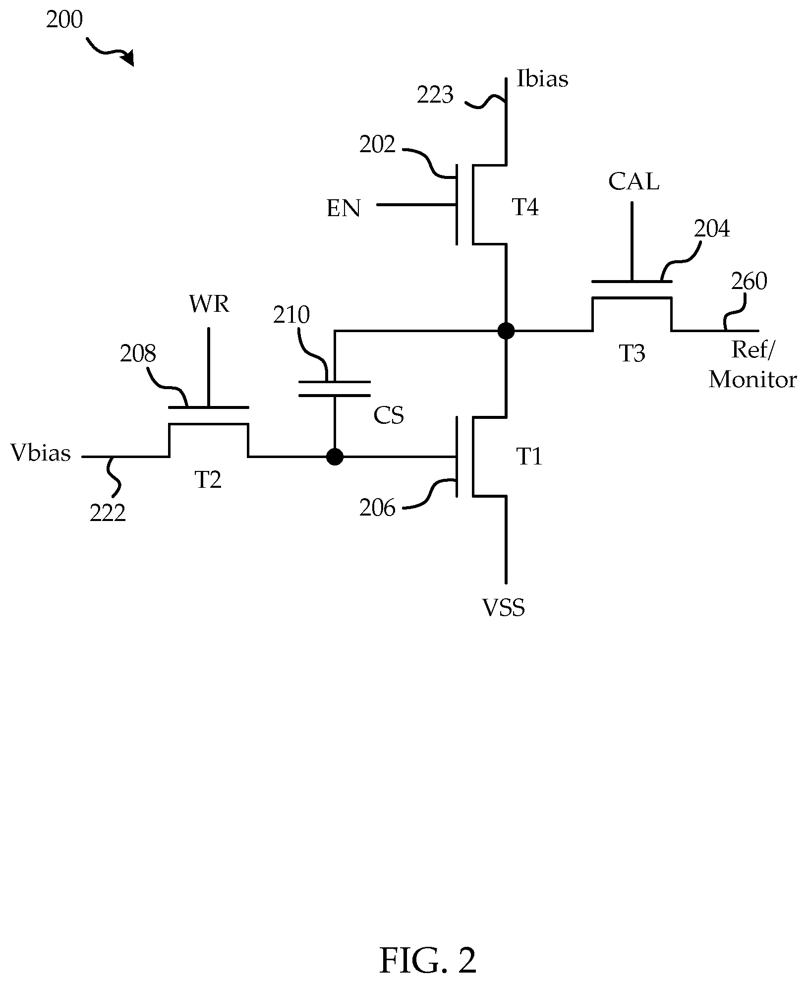
FIG. 2 is a circuit diagram of a current sink according to one embodiment;
FIG. 3 is a timing diagram of current sink and source programming and calibration according to one embodiment;
FIG. 4 is a circuit diagram of a current source according to a further embodiment;
FIG. 5 is a circuit diagram of a 4T1C pixel circuit according to an embodiment;
FIG. 6A is a timing diagram illustrating a programming and driving of a 4T1C pixel circuit;
FIG. 6B is a timing diagram illustrating a programming and measuring of a 4T1C pixel circuit;
FIG. 7 is a circuit diagram of a 6T1C pixel circuit according to an embodiment;
FIG. 8A is a timing diagram illustrating a programming and driving of a 6T1C pixel circuit;
FIG. 8B is a timing diagram illustrating a programming and measuring of a 6T1C pixel circuit;
FIG. 9 is a timing diagram for improved driving of rows of pixels;
FIG. 10 is a circuit diagram of a 4T1C pixel circuit operated in current mode according to an embodiment;
FIG. 11 is a circuit diagram of a 6T1C pixel circuit operated in current mode according to an embodiment;
FIG. 12 is a timing diagram illustrating a programming and driving of 4T1C and 6T1C pixel circuits of FIG. 10 and FIG. 11.
FIG. 13 is a circuit diagram of a 4T1C reference current sink according to an embodiment;
FIG. 14 is a circuit diagram of a 6T1C reference current sink according to an embodiment;
FIG. 15 is a circuit diagram of a 4T1C reference current source according to an embodiment;
FIG. 16 is a circuit diagram of a 6T1C reference current source according to an embodiment;
FIG. 17 is a reference row timing diagram illustrating a programming and driving of 4T1C, 6T1C, sinks and sources of FIGS. 13, 14, 15, and 16;
FIG. 18 is a schematic diagram of on-panel multiplexing of data and monitor lines;
FIG. 19 is a schematic diagram of on-panel multiplexing of data and monitor lines;
FIG. 20 is a timing diagram illustrating a programming a driving of pixel circuits of FIG. 19; and
FIG. 21 is a schematic diagram of modified on-panel multiplexing of data and monitor lines, in which two pixels are programmed in a single cycle.
While the present disclosure is susceptible to various modifications and alternative forms, specific embodiments or implementations have been shown by way of example in the drawings and will be described in detail herein. It should be understood, however, that the disclosure is not intended to be limited to the particular forms disclosed. Rather, the disclosure is to cover all modifications, equivalents, and alternatives falling within the spirit and scope of an invention as defined by the appended claims.
DETAILED DESCRIPTION
Many modern display technologies suffer from defects, variations, and non-uniformities, from the moment of fabrication, and can suffer further from aging and deterioration over the operational lifetime of the display, which result in the production of images which deviate from those which are intended. Methods of image calibration and compensation are used to correct for those defects in order to produce images which are more accurate, uniform, or otherwise more closely reproduce the image represented by the image data. Some displays utilize a current-bias voltage-programming driving scheme, each of its pixels being a current-biased voltage-programmed (CBVP) pixel. In such displays a further requirement for producing and maintaining accurate image reproduction is that the current biasing elements, that is the current sources or sinks, which provide current biasing provide the appropriate level of current biasing to those pixels.
Due to unavoidable variations in fabrication and variations in degradation through use, a number of current biasing elements provided for a display and pixels of the display, although designed to be uniformly and exactly alike and programmed to provide the desired current biasing level and respectively desired luminance, in fact exhibit deviations in current biasing and respectively luminance provided. In order to correct for visual defects that would otherwise arise from the non-uniformity and inaccuracies of these current sources or sinks and the pixels, the programming of the current biasing elements and pixels are augmented with calibration and optionally monitoring and compensation.
As the resolution of an array semiconductor device increases, the number of lines and elements required to drive, calibrate, and/or monitor the array increases dramatically. This can result in higher power consumption, higher manufacturing costs, and a larger physical foot print. In the case of a CBVP pixel display, providing circuitry to program, calibrate, and monitor current sources or sinks can increase cost and complexity of integration as the number of rows or columns increases.
The systems and methods disclosed below address these issues through control timing and calibration of pixel circuits and a family of current biasing elements while utilizing circuits which are integrated on the display in a manner which use existing display components.
While the embodiments described herein will be in the context of AMOLED displays it should be understood that the systems and methods described herein are applicable to any other display comprising pixels which might utilize current biasing, including but not limited to light emitting diode displays (LED), electroluminescent displays (ELD), organic light emitting diode displays (OLED), plasma display panels (PSP), among other displays.
It should be understood that the embodiments described herein pertain to systems and methods of calibration and compensation and do not limit the display technology underlying their operation and the operation of the displays in which they are implemented. The systems and methods described herein are applicable to any number of various types and implementations of various visual display technologies.
FIG. 1 is a diagram of an example display system 150 implementing the methods and comprising the circuits described further below. The display system 150 includes a display panel 120, an address driver 108, a source driver 104, a controller 102, and a memory storage 106.
The display panel 120 includes an array of pixels 110a 110b (only two explicitly shown) arranged in rows and columns. Each of the pixels 110a 110b is individually programmable to emit light with individually programmable luminance values and is a current biased voltage programmed pixel (CBVP). The controller 102 receives digital data indicative of information to be displayed on the display panel 120. The controller 102 sends signals 132 to the source driver 104 and scheduling signals 134 to the address driver 108 to drive the pixels 110 in the display panel 120 to display the information indicated. The plurality of pixels 110 of the display panel 120 thus comprise a display array or display screen adapted to dynamically display information according to the input digital data received by the controller 102. The display screen can display images and streams of video information from data received by the controller 102. The supply voltage 114 provides a constant power voltage or can serve as an adjustable voltage supply that is controlled by signals from the controller 102. The display system 150 incorporates features from current biasing elements 155a, 155b, either current sources or sinks (current sinks are shown) to provide biasing currents to the pixels 110a 110b in the display panel 120 to thereby decrease programming time for the pixels 110. Although shown separately from the source driver 104, current biasing elements 155a, 155b may form part of the source driver 104 or may be integrated as separate elements. It is to be understood that the current biasing elements 155a, 155b used to provide current biasing to the pixels may be current sources rather than current sinks depicted in FIG. 1.
For illustrative purposes, only two pixels 110a, 110b are explicitly shown in the display system 150 in FIG. 1. It is understood that the display system 150 is implemented with a display screen that includes an array of pixels, such as the pixels 110a, 110b, and that the display screen is not limited to a particular number of rows and columns of pixels. For example, the display system 150 can be implemented with a display screen with a number of rows and columns of pixels commonly available in displays for mobile devices, monitor-based devices, and/or projection-devices. In a multichannel or color display, a number of different types of pixels, each responsible for reproducing color of a particular channel or color such as red, green, or blue, will be present in the display. Pixels of this kind may also be referred to as "subpixels" as a group of them collectively provide a desired color at a particular row and column of the display, which group of subpixels may collectively also be referred to as a "pixel".
Each pixel 110a, 110b is operated by a driving circuit or pixel circuit that generally includes a driving transistor and a light emitting device. Hereinafter the pixel 110a, 110b may refer to the pixel circuit. The light emitting device can optionally be an organic light emitting diode, but implementations of the present disclosure apply to pixel circuits having other electroluminescence devices, including current-driven light emitting devices and those listed above. The driving transistor in the pixel 110a, 110b can optionally be an n-type or p-type amorphous silicon thin-film transistor, but implementations of the present disclosure are not limited to pixel circuits having a particular polarity of transistor or only to pixel circuits having thin-film transistors. The pixel circuit 110a, 110b can also include a storage capacitor for storing programming information and allowing the pixel circuit 110 to drive the light emitting device after being addressed. Thus, the display panel 120 can be an active matrix display array.
As illustrated in FIG. 1, each of the pixels 110a, 110b in the display panel 120 are coupled to a respective select line 124a, 124b, a respective supply line 126a, 126b, a respective data line 122a, 122b, a respective current bias line 123a, 123b, and a respective monitor line 128a, 128b. A read line may also be included for controlling connections to the monitor line. In one implementation, the supply voltage 114 can also provide a second supply line to each pixel 110a, 110b. For example, each pixel can be coupled to a first supply line 126a, 126b charged with Vdd and a second supply line 127a, 127b coupled with Vss, and the pixel circuits 110a, 110b can be situated between the first and second supply lines to facilitate driving current between the two supply lines during an emission phase of the pixel circuit. It is to be understood that each of the pixels 110 in the pixel array of the display 120 is coupled to appropriate select lines, supply lines, data lines, and monitor lines. It is noted that aspects of the present disclosure apply to pixels having additional connections, such as connections to additional select lines, and to pixels having fewer connections, and pixels sharing various connections.
With reference to the pixel 110a of the display panel 120, the select line 124a is provided by the address driver 108, and can be utilized to enable, for example, a programming operation of the pixel 110a by activating a switch or transistor to allow the data line 122a to program the pixel 110a. The data line 122a conveys programming information from the source driver 104 to the pixel 110a. For example, the data line 122a can be utilized to apply a programming voltage or a programming current to the pixel 110a in order to program the pixel 110a to emit a desired amount of luminance. The programming voltage (or programming current) supplied by the source driver 104 via the data line 122a is a voltage (or current) appropriate to cause the pixel 110a to emit light with a desired amount of luminance according to the digital data received by the controller 102. The programming voltage (or programming current) can be applied to the pixel 110a during a programming operation of the pixel 110a so as to charge a storage device within the pixel 110a, such as a storage capacitor, thereby enabling the pixel 110a to emit light with the desired amount of luminance during an emission operation following the programming operation. For example, the storage device in the pixel 110a can be charged during a programming operation to apply a voltage to one or more of a gate or a source terminal of the driving transistor during the emission operation, thereby causing the driving transistor to convey the driving current through the light emitting device according to the voltage stored on the storage device. Current biasing element 155a provides a biasing current to the pixel 110a over the current bias line 123a in the display panel 120 to thereby decrease programming time for the pixel 110a. The current biasing element 155a is also coupled to the data line 122a and uses the data line 122a to program its current output when not in use to program the pixels, as described hereinbelow. In some embodiments, the current biasing elements 155a, 155b are also coupled to a reference/monitor line 160 which is coupled to the controller 102, for monitoring and controlling of the current biasing elements 155a, 155b.
Generally, in the pixel 110a, the driving current that is conveyed through the light emitting device by the driving transistor during the emission operation of the pixel 110a is a current that is supplied by the first supply line 126a and is drained to a second supply line 127a. The first supply line 126a and the second supply line 127a are coupled to the voltage supply 114. The first supply line 126a can provide a positive supply voltage (e.g., the voltage commonly referred to in circuit design as "Vdd") and the second supply line 127a can provide a negative supply voltage (e.g., the voltage commonly referred to in circuit design as "Vss"). Implementations of the present disclosure can be realized where one or the other of the supply lines (e.g., the supply line 127a) is fixed at a ground voltage or at another reference voltage.
The display system 150 also includes a monitoring system 112. With reference again to the pixel 110a of the display panel 120, the monitor line 128a connects the pixel 110a to the monitoring system 112. The monitoring system 112 can be integrated with the source driver 104, or can be a separate stand-alone system. In particular, the monitoring system 112 can optionally be implemented by monitoring the current and/or voltage of the data line 122a during a monitoring operation of the pixel 110a, and the monitor line 128a can be entirely omitted. The monitor line 128a allows the monitoring system 112 to measure a current or voltage associated with the pixel 110a and thereby extract information indicative of a degradation or aging of the pixel 110a or indicative of a temperature of the pixel 110a. In some embodiments, display panel 120 includes temperature sensing circuitry devoted to sensing temperature implemented in the pixels 110a, while in other embodiments, the pixels 110a comprise circuitry which participates in both sensing temperature and driving the pixels. For example, the monitoring system 112 can extract, via the monitor line 128a, a current flowing through the driving transistor within the pixel 110a and thereby determine, based on the measured current and based on the voltages applied to the driving transistor during the measurement, a threshold voltage of the driving transistor or a shift thereof. In some embodiments the monitoring system 112 extracts information regarding the current biasing elements via data lines 122a, 122b or the reference/monitor line 160 and in some embodiments, this is performed in cooperation with or by the controller 102.
The monitoring system 112 can also extract an operating voltage of the light emitting device (e.g., a voltage drop across the light emitting device while the light emitting device is operating to emit light). The monitoring system 112 can then communicate signals 132 to the controller 102 and/or the memory 106 to allow the display system 150 to store the extracted aging information in the memory 106. During subsequent programming and/or emission operations of the pixel 110a, the aging information is retrieved from the memory 106 by the controller 102 via memory signals 136, and the controller 102 then compensates for the extracted degradation information in subsequent programming and/or emission operations of the pixel 110a. For example, once the degradation information is extracted, the programming information conveyed to the pixel 110a via the data line 122a can be appropriately adjusted during a subsequent programming operation of the pixel 110a such that the pixel 110a emits light with a desired amount of luminance that is independent of the degradation of the pixel 110a. In an example, an increase in the threshold voltage of the driving transistor within the pixel 110a can be compensated for by appropriately increasing the programming voltage applied to the pixel 110a. In a similar manner, the monitoring system 112 can extract the bias current of a current biasing element 155a. The monitoring system 112 can then communicate signals 132 to the controller 102 and/or the memory 106 to allow the display system 150 to store the extracted information in the memory 106. During subsequent programming of the current biasing element 155a, the information is retrieved from the memory 106 by the controller 102 via memory signals 136, and the controller 102 then compensates for the errors in current previously measured using adjustments in subsequent programming of the current biasing element 155a.
Referring to FIG. 2, the structure of a current sink 200 circuit according to an embodiment will now be described. The current sink 200 corresponds, for example, to a single current biasing element 155a, 155b of the display system 150 depicted in FIG. 1 which provides a bias current Ibias over current bias lines 123a, 123b to a CBVP pixel 110a, 110b. The current sink 200 depicted in FIG. 2 is based on PMOS transistors. A PMOS based current source is also contemplated, structured and functioning according to similar principles described here. It should be understood that variations of this current sink and its functioning are contemplated and include different types of transistors (PMOS, NMOS, or CMOS) and different semiconductor materials (e.g., LTPS, Metal Oxide, etc.).
The current sink 200 includes a first switch transistor 202 (T4) controlled by an enable signal EN coupled to its gate terminal, and being coupled via one of a source and drain terminal to a current bias line 223 (Ibias) corresponding to, for example, a current bias line 123a of FIG. 1, and coupled via the other of the source and drain terminals of the first switch transistor 202 to a first terminal of a storage capacitance 210. A gate terminal of a current drive transistor 206 (T1) is coupled to a second terminal of the storage capacitance 210, while one of the source and gate terminals of the current drive transistor 206 is coupled to the first terminal of the storage capacitance 210. The other of the source and gate terminals of the current drive transistor 206 is coupled to VSS. A gate terminal of a second switch transistor 208 (T2) is coupled to a write signal line (WR), while one of its source and drain terminals is coupled to a voltage bias or data line (Vbias) 222, corresponding, for example, to data line 122a depicted in FIG. 1. The other of the source and drain terminals of the second switch transistor 208 is coupled to the second terminal of the storage capacitance 210. A gate terminal of a third switch transistor 204 (T3) is coupled to a calibration control line (CAL), while one of its source and drain terminals is coupled to a reference monitor line 260, corresponding, for example, to reference monitor line 160 depicted in FIG. 1. The other of the source and drain terminals of the third switch transistor 204 is coupled to the first terminal of the storage capacitance 210. As mentioned above the data lines are shared, being used for providing voltage biasing or data for the pixels during certain time periods during a frame and being used for providing voltage biasing for the current biasing element, here a current sink, during other time periods of a frame. This re-use of the data lines allows for the added benefits of programming and compensation of the numerous individual current sinks using only one extra reference monitoring line 160.
With reference also to FIG. 3, an example of a timing of a current control cycle 300 for programming and calibrating the current sink 200 depicted in FIG. 2 will now be described. The complete control cycle 300 occurs typically once per frame and includes four smaller cycles, a disconnect cycle 302, a programming cycle 304, a calibration cycle 306, and a settling cycle 308. During the disconnect cycle 302, the current sink 200 ceases to provide biasing current Ibias to the current bias line 223 in response to the EN signal going high and the first transistor switch 202 turning off. By virtue of the CAL and WR signals being high, both the second and third switch transistors 208, 204 remain off. The duration of the disconnect cycle 302 also provides a settling time for the current sink 200 circuit. The EN signal remains high throughout the entire control cycle 300, only going low once the current sink 200 circuit has been programmed, calibrated, and settled and is ready to provide the bias current over the current bias line 223. Once the current sink 200 has settled after the disconnect cycle 302 has completed, the programming cycle 304 begins with the WR signal going low turning on the second switch transistor 208 and with the CAL signal going low turning on the third switch transistor 204. During the programming cycle 304 therefore, the third switch transistor 204 connects the reference monitor line 260 over which there is transmitted a known reference signal (can be voltage or current) to the first terminal of the storage capacitance 210, while the second switch transistor 208 connects the voltage bias or data line 222 being input with voltage Vbias to the gate terminal of the current driving transistor 206 and the second terminal of the storage capacitance 210. As a result, the storage capacitance 210 is charged to a defined value. This value is roughly that which is anticipated as necessary to control the current driving transistor 206 to deliver the appropriate current biasing Ibias taking into account optional calibration described below.
After the programming cycle 304 and during the calibration cycle 306, the circuit is reconfigured to discharge some of the voltage (charge) of the storage capacitance 210 though the current driving transistor 206. The calibration signal CAL goes high, turning off the third switch transistor 204 and disconnecting the first terminal of the storage capacitance 210 from the reference monitor line 260. The amount discharged is a function of the main element of the current sink 200, namely the current driving transistor 206 or its related components. For example, if the current driving transistor 206 is "strong", the discharge occurs relatively quickly and relatively more charge is discharged from the storage capacitance 210 through the current driving transistor 206 during the fixed duration of the calibration cycle 306. On the other hand, if the current driving transistor 206 is "weak", the discharge occurs relatively slowly and relatively less charge is discharged from the storage capacitance 210 through the current driving transistor 206 during the fixed duration of the calibration cycle 306. As a result the voltage (charge) stored in the storage capacitance 210 is reduced comparatively more for relatively strong current driving transistors versus comparatively less for relatively weak current driving transistors thereby providing some compensation for non-uniformity and variations in current driving transistors across the display whether due to variations in fabrication or variations in degradation over time.
After the calibration cycle 306, a settling cycle 308 is performed prior to provision of the biasing current Ibias to the current bias line 223. During the settling cycle 308, the first and third switch transistors 202, 204 remain off while the WR signal goes high to also turn the second switch transistor 208 off. After completion of the duration of the settling cycle 308, the enable signal EN goes low turning on the first switch transistor 202 and allowing the current driving transistor 206 to sink the Ibias current on the current bias line 223 according to the voltage (charge) stored in the storage capacitance 210, which as mentioned above, has a value which has been drained as a function of the current driving transistor 206 in order to provide compensation for the specific characteristics of the current driving transistor 206.
In some embodiments, the calibration cycle 306 is eliminated. In such a case, the compensation manifested as a change in the voltage (charge) stored by the storage capacitance 210 as a function of the characteristics of the current driving transistor 206 is not automatically provided. In such a case a form of manual compensation may be utilized in combination with monitoring.
In some embodiments, after a current sink 200 has been programmed, and prior to providing the biasing current over the current bias line 223, the current of the current sink 200 is measured through the reference monitor line 260 by controlling the CAL signal to go low, turning on the third switch transistor 204. As illustrated in FIG. 1, in some embodiments the reference monitor line 160 is shared and hence during measurement of the current sink 200 of interest all other current sinks are programmed or otherwise controlled such that they do not source or sink any current on the reference monitor line 160. Once the current of the current sink 200 has been measured in response to known programming of the current sink 200 and possibly after a number of various current measurements in response to various programming values have been measured and stored in memory 106, the controller 102 and memory 106 (possibly in cooperation with other components of the display system 150) adjusts the voltage Vbias used to program the current sink 200 to compensate for the deviations from the expected or desired current sinking exhibited by the current sink 200. This monitoring and compensation, need not be performed every frame and can be performed in a periodic manner over the lifetime of the display to correct for degradation of the current sink 200.
In some embodiments a combination of calibration and monitoring and compensation is used. In such a case the calibration can occur every frame in combination with periodic monitoring and compensation.
Referring to FIG. 4, the structure of a current source 400 circuit according to an embodiment will now be described. The current source 400 corresponds, for example, to a single current biasing element 155a, 155b of the display system 150 depicted in FIG. 1 which provides a bias current Ibias over current bias lines 123a, 123b to a CBVP pixel 110a, 110b. As is described in more detail below, the connections and manner of integration of current source 400 into the display system 150 is slightly different from that depicted in FIG. 1 for a current sink 200. The current source 400 depicted in FIG. 4 is based on PMOS transistors. It should be understood that variations of this current source and its functioning are contemplated and include different types of transistors (PMOS, NMOS, or CMOS) and different semiconductor materials (e.g., LTPS, Metal Oxide, etc.).
The current source 400 includes a first switch transistor 402 (T4) controlled by an enable signal EN coupled to its gate terminal, and being coupled via one of a source and drain terminal of the first transistor switch 402 to a current bias line 423 (Ibias) corresponding to, for example, a current bias line 123a of FIG. 1. A gate terminal of a current drive transistor 406 (T1) is coupled to a first terminal of a storage capacitance 410, while a first of the source and drain terminals of the current drive transistor 406 is coupled to the other of the source and drain terminals of the first switch transistor 402, and a second of the source and drain terminals of the current drive transistor 406 is coupled to a second terminal of the storage capacitance 410. The second terminal of the storage capacitance 410 is coupled to VDD. A gate terminal of a second switch transistor 408 (T2) is coupled to a write signal line (WR), while one of its source and drain terminals is coupled to the first terminal of the storage capacitance 410 and the other of its source and drain terminals is coupled to the first of the source and drain terminals of the current driving transistor 406. A gate terminal of a third switch transistor 404 (T3) is coupled to a calibration control line (CAL), while one of its source and drain terminals is coupled to a voltage bias monitor line 460, corresponding, for example, to voltage bias or data lines 122a, 122b depicted in FIG. 1. The other of the source and drain terminals of the third switch transistor 404 is coupled to the first of the source and drain terminals of the current drive transistor 406.
In the embodiment depicted in FIG. 4, the current source is not coupled to a reference monitor line 160 such as that depicted in FIG. 1. Instead of the current source 400 being programmed with Vbias and a reference voltage as in the case of the current sink 200, the storage capacitance 410 of the current source 400 is programmed to a defined value using the voltage bias signal Vbias provided over the voltage bias or data line 122a and VDD. In this embodiment the data lines 122a, 122b serve as monitor lines as and when needed.
Referring once again to FIG. 3, an example of a timing of a current control cycle 300 for programming and calibrating the current source 400 depicted in FIG. 4 will now be described. The timing of the current control cycle 300 for programming the current source 400 of FIG. 4 is the same as that for the current sink 200 of FIG. 2.
The complete control cycle 300 occurs typically once per frame and includes four smaller cycles, a disconnect cycle 302, a programming cycle 304, a calibration cycle 306, and a settling cycle 308. During the disconnect cycle 302, the current source 400 ceases to provide biasing current Ibias to the current bias line 423 in response to the EN signal going high and the first transistor switch 402 turning off. By virtue of the CAL and WR signals being high, both the second and third switch transistors 408, 404 remain off. The duration of the disconnect cycle 402 also provides a settling time for the current source 400 circuit. The EN signal remains high throughout the entire control cycle 300, only going low once the current source 400 circuit has been programmed, calibrated, and settled and is ready to provide the bias current over the current bias line 423. Once the current source 400 has settled after the disconnect cycle 302 has completed, the programming cycle 304 begins with the WR signal going low turning on the second switch transistor 408 and with the CAL signal going low turning on the third switch transistor 404. During the programming cycle 304 therefore, the third switch transistor 404 and the second switch transistor 408 connects the voltage bias monitor line 460 over which there is transmitted a known Vbias signal to the first terminal of the storage capacitance 410. As a result, since the second terminal of the storage capacitance 410 is coupled top VDD, the storage capacitance 410 is charged to a defined value. This value is roughly that which is anticipated as necessary to control the current driving transistor 406 to deliver the appropriate current biasing Ibias taking into account optional calibration described below.
After the programming cycle 304 and during the calibration cycle 306, the circuit is reconfigured to discharge some of the voltage (charge) of the storage capacitance 410 though the current driving transistor 406. The calibration signal CAL goes high, turning off the third switch transistor 404 and disconnecting the first terminal of the storage capacitance 410 from the voltage bias monitor line 460. The amount discharged is a function of the main element of the current source 400, namely the current driving transistor 406 or its related components. For example, if the current driving transistor 406 is "strong", the discharge occurs relatively quickly and relatively more charge is discharged from the storage capacitance 410 through the current driving transistor 406 during the fixed duration of the calibration cycle 306. On the other hand, if the current driving transistor 406 is "weak," the discharge occurs relatively slowly and relatively less charge is discharged from the storage capacitance 410 through the current driving transistor 406 during the fixed duration of the calibration cycle 306. As a result, the voltage (charge) stored in the storage capacitance 410 is reduced comparatively more for relatively strong current driving transistors versus comparatively less for relatively weak current driving transistors thereby providing some compensation for non-uniformity and variations in current driving transistors across the display whether due to variations in fabrication or degradation over time.
After the calibration cycle 306, a settling cycle 308 is performed prior to provision of the biasing current Ibias to the current bias line 423. During the settling cycle, the first and third switch transistors 402, 404 remain off while the WR signal goes high to also turn the second switch transistor 408 off. After completion of the duration of the settling cycle 308, the enable signal EN goes low turning on the first switch transistor 402 and allowing the current driving transistor 406 to source the Ibias current on the current bias line 423 according to the voltage (charge) stored in the storage capacitance 410, which as mentioned above, has a value which has been drained as a function of the current driving transistor 406 in order to provide compensation for the specific characteristics of the current driving transistor 406.
In some embodiments, the calibration cycle 306 is eliminated. In such a case, the compensation manifested as a change in the voltage (charge) stored by the storage capacitance 410 as a function of the characteristics of the current driving transistor 406 is not automatically provided. In such a case, as with the embodiment above in the context of a current sink 200 a form of manual compensation may be utilized in combination with monitoring for the current source 400.
In some embodiments, after a current source 400 has been programmed, and prior to providing the biasing current over the current bias line 423, the current of the current source 400 is measured through the voltage bias monitor line 460 by controlling the CAL signal to go low, turning on the third switch transistor 404.
Once the current of the current source 400 has been measured in response to known programming of the current source 400 and possibly after a number of various current measurements in response to various programming values have been measured and stored in memory 106, the controller 102 and memory 106 (possibly in cooperation with other components of the display system 150) adjusts the voltage Vbias used to program the current source 400 to compensate for the deviations from the expected or desired current sourcing exhibited by the current source 400. This monitoring and compensation, need not be performed every frame and can be performed in a periodic manner over the lifetime of the display to correct for degradation of the current source 400.
Although the current sink 200 of FIG. 2 and the current source 400 of FIG. 4 have each been depicted as possessing a single current driving transistor 206, 406 it should be understood that each may comprise a cascaded transistor structure for providing the same functionality as shown and described in association with FIG. 2 and FIG. 4.
With reference to FIG. 5, the structure of a four transistor, single capacitor (4T1C) pixel circuit 500 according to an embodiment will now be described. The 4T1C pixel circuit 500 corresponds, for example, to a single pixel 110a of the display system 150 depicted in FIG. 1 which in some embodiments is not necessarily a current biased pixel. The 4T1C pixel circuit 500 depicted in FIG. 5 is based on NMOS transistors. It should be understood that variations of this pixel and its functioning are contemplated and include different types of transistors (PMOS, NMOS, or CMOS) and different semiconductor materials (e.g. LTPS, Metal Oxide, etc.).
The 4T1C pixel circuit 500 includes a driving transistor 510 (T1), a light emitting device 520, a first switch transistor 530 (T2), a second switch transistor 540 (T3), a third switch transistor 550 (T4), and a storage capacitor 560 (C.sub.S). Each of the driving transistor 510, the first switch transistor 530, the second switch transistor 540, and the third switch transistor 550 having first, second, and gate terminals, and each of the light emitting device 520 and the storage capacitor 560 having first and second terminals.
The gate terminal of the driving transistor 510 is coupled to a first terminal of the storage capacitor 560, while the first terminal of the driving transistor 510 is coupled to the second terminal of the storage capacitor 560, and the second terminal of the driving transistor 510 is coupled to the first terminal of the light emitting device 520. The second terminal of the light emitting device 520 is coupled to a first reference potential ELVSS. A capacitance of the light-emitting device 520 is depicted in FIG. 5 as C.sub.LD. In some embodiments, the light emitting device 520 is an OLED. The gate terminal of the first switch transistor 530 is coupled to a write signal line (WR), while the first terminal of the first switch transistor 530 is coupled to a data signal line (V.sub.DATA), and the second terminal of the first switch transistor 530 is coupled to the gate terminal of the driving transistor 510. A node common to the gate terminal of the driving transistor 510 and the storage capacitor 560 as well as the first switch transistor 530 is labelled by its voltage V.sub.G in the figure. The gate terminal of the second switch transistor 540 is coupled to a read signal line (RD), while the first terminal of the second switch transistor 540 is coupled to a monitor signal line (V.sub.MON), and the second terminal of the second switch transistor 540 is coupled to the second terminal of the storage capacitor 560. The gate terminal of the third switch transistor 550 is coupled to an emission signal line (EM), while the first terminal of the third switch transistor 550 is coupled to a second reference potential ELVDD, and the second terminal of the third switch transistor 550 is coupled to the second terminal of the storage capacitor 560. A node common to the second terminal of the storage capacitor 560, the driving transistor 510, the second switch transistor 540, and the third switch transistor 550 is labelled by its voltage Vs in the figure.
With reference also to FIG. 6A, an example of a display timing 600A for the 4T1C pixel circuit 500 depicted in FIG. 5 will now be described. The complete display timing 600A occurs typically once per frame and includes a programming cycle 602A, a calibration cycle 604A, a settling cycle 606A, and an emission cycle 608A. During the programming cycle 602A over a period T.sub.RD, the read signal (RD) and write signal (WR) are held low while the emission (EM) signal is held high. The emission signal (EM) is held high throughout the programming, calibration, and settling cycles 602A 604A 606A to ensure the third switch transistor 550 remains off during those cycles (T.sub.EM).
During the programming cycle 602A the first switch transistor 530 and the second switch transistor 540 are both on. The voltage of the storage capacitor 560 and therefore the voltage V.sub.SG of the driving transistor 510 is charged to a value of V.sub.MON-V.sub.DATA where V.sub.MON is a voltage of the monitor line and V.sub.DATA is a voltage of the data line. These voltages are set in accordance with a desired programming voltage for causing the pixel 500 to emit light at a desired luminance according to image data.
At the beginning of the calibration cycle 604A, the read line (RD) goes high to turn off the second switch transistor 540 to discharge some of the voltage (charge) of the storage capacitor 560 through the driving transistor 510. The amount discharged is a function of the characteristics of the driving transistor 510. For example, if the driving transistor 510 is "strong", the discharge occurs relatively quickly and relatively more charge is discharged from the storage capacitor 560 through the driving transistor 510 during the fixed duration T.sub.IPC of the calibration cycle 604A. On the other hand, if the driving transistor 510 is "weak", the discharge occurs relatively slowly and relatively less charge is discharged from the storage capacitor 560 through the driving transistor 510 during the calibration cycle 604A. As a result, the voltage (charge) stored in the storage capacitor 560 is reduced comparatively more for relatively strong driving transistors versus comparatively less for relatively weak driving transistors, thereby providing some compensation for non-uniformity and variations in the driving transistors across the display whether due to variations in fabrication or variations in degradation over time.
After the calibration cycle 604A, a settling cycle 606A is performed prior to the emission. During the settling cycle 606A the second and third switch transistors 540, 550 remain off, while the write signal (WR) goes high to also turn off the first switch transistor 530. After completion of the duration of the settling cycle 606A at the start of the emission cycle 608A, the emission signal (EM) goes low turning on the third switch transistor 550 allowing current to flow through the light emitting device 520 according to the calibrated stored voltage on the storage capacitor 560.
With reference also to FIG. 6B, an example of a measurement timing 600B for the 4T1C pixel circuit 500 depicted in FIG. 5 will now be described. The complete measurement timing 600B occurs typically in the same time period as a display frame and includes a programming cycle 602B, a calibration cycle 604B, a settling cycle 606B, and a measurement cycle 610B. The programming cycle 602B, calibration cycle 604B, settling cycle 606B, are performed substantially the same as described above in connection with FIG. 6A, however, a number of the voltages set for V.sub.DATA, V.sub.MON, and stored on the storage capacitor 560 are determined with the goal of measuring the pixel circuit 500 instead of displaying any particular luminance according to image data.
Once the programming cycle 602B, calibration cycle 604B, and settling cycle 606B are completed, a measuring cycle 610B having duration T.sub.MS commences. At the beginning of the measuring cycle 610B, the emission signal (EM) goes high turning off the third switch transistor 550, while the read signal (RD) goes low turning on the second switch transistor 540 to provide read access to the monitor line.
For measurement of the driving transistor 510, the programming voltage V.sub.SG for the driving transistor 510 is set to the desired level through the programming 602B, and calibration 604B cycles, and then during the duration T.sub.MS of the measurement cycle 610B the current/charge is observed on the monitor line V.sub.MON. The voltage V.sub.MON on the monitor line is kept at a high enough level in order to operate the driving transistor 510 in saturation mode for measurement of the driving transistor 510.
For measurement of the light emitting device 520, the programming voltage V.sub.SG for the driving transistor 510 is set to the highest possible voltage available on the data line V.sub.DATA, for example a value corresponding to peak-white gray-scale, through the programming 602B, and calibration 604B cycles, in order to operate the driving transistor 510 in the triode region (switch mode). In this condition, during the duration T.sub.MS of the measurement cycle 610B the voltage/current of the light emitting device 520 can be directly modulated/measured through the monitor line.
With reference to FIG. 7, the structure of a six transistor, single capacitor (6T1C) pixel circuit 700 according to an embodiment will now be described. The 6T1C pixel circuit 700 corresponds, for example, to a single pixel 110a of the display system 150 depicted in FIG. 1 which in some embodiments is not necessarily a current biased pixel. The 6T1C pixel circuit 700 depicted in FIG. 7 is based on NMOS transistors. It should be understood that variations of this pixel and its functioning are contemplated and include different types of transistors (PMOS, NMOS, or CMOS) and different semiconductor materials (e.g. LTPS, Metal Oxide, etc.).
The 6T1C pixel circuit 700 includes a driving transistor 710 (T1), a light emitting device 720, a storage capacitor 730 (C.sub.S), a first switch transistor 740 (T2), a second switch transistor 750 (T3), a third switch transistor 760 (T4), a fourth switch transistor 770 (T5), and a fifth switch transistor 780 (T6). Each of the driving transistor 710, the first switch transistor 740, the second switch transistor 750, the third switch transistor 760, the fourth switch transistor 770, and the fifth switch transistor 780, having first, second, and gate terminals, and each of the light emitting device 720 and the storage capacitor 730 having first and second terminals.
The gate terminal of the driving transistor 710 is coupled to a first terminal of the storage capacitor 730, while the first terminal of the driving transistor 710 is coupled to a first reference potential ELVDD, and the second terminal of the driving transistor 710 is coupled to the first terminal of the third switch transistor 760. The gate terminal of the third switch transistor 760 is coupled to a read signal line (RD) and the second terminal of the third switch transistor 760 is coupled to a monitor/reference current line V.sub.MON/I.sub.REF. The gate terminal of the fourth switch transistor 770 is coupled to an emission signal line (EM), while the first terminal of the fourth switch transistor 770 is coupled to the first terminal of the third switch transistor 760, and the second terminal of the fourth switch transistor 770 is coupled to the first terminal of the light emitting device 720. A second terminal of the light emitting device 720 is coupled to a second reference potential ELVSS. A capacitance of the light-emitting device 720 is depicted in FIG. 7 as C.sub.LD. In some embodiments, the light emitting device 720 is an OLED. The gate terminal of the first switch transistor 740 is coupled to a write signal line (WR), while the first terminal of the first switch transistor 740 is coupled to the first terminal of the storage capacitor 730, and the second terminal of the first switch transistor 740 is coupled to the first terminal of the third switch transistor 760. The gate terminal of the second switch transistor 750 is coupled to the write signal line (WR), while the first terminal of the second switch transistor 750 is coupled to a data signal line (V.sub.DATA), and the second terminal of the second switch transistor 750 is coupled to the second terminal of the storage capacitor 730. A node common to the gate terminal of the driving transistor 710 and the storage capacitor 730 as well as the first switch transistor 740 is labelled by its voltage V.sub.G in the figure. The gate terminal of the fifth switch transistor 780 is coupled to the emission signal line (EM), while the first terminal of the fifth switch transistor 780 is coupled to reference potential VBP, and the second terminal of the fifth switch transistor 780 is coupled to the second terminal of the storage capacitor 730. A node common to the second terminal of the storage capacitor 730, the second switch transistor 750, and the fifth switch transistor 780 is labelled by its voltage V.sub.CB in FIG. 7.
With reference also to FIG. 8A, an example of a display timing 800A for the 6T1C pixel circuit 700 depicted in FIG. 7 will now be described. The complete display timing 800A occurs typically once per frame and includes a programming cycle 802A, a calibration cycle 804A, a settling cycle 806A, and an emission cycle 808A. During the programming cycle 802A over a period T.sub.RD, the read signal (RD) and write signal (WR) are held low while the emission (EM) signal is held high. The emission signal (EM) is held high throughout the programming, calibration, and settling cycles 802A 804A 806A to ensure the fourth switch transistor 770 and the fifth switch transistor 780 remain off during those cycles (T.sub.EM).
During the programming cycle 802A the first switch transistor 740, the second switch transistor 750, and the third switch transistor 760 are all on. The voltage of the storage capacitor 730 V.sub.CS is charged to a value of V.sub.CB-V.sub.G=V.sub.DATA-(V.sub.DD-V.sub.SG(T1)).apprxeq.V.su- b.DATA-V.sub.DD+V.sub.th(T1), where V.sub.DATA is a voltage on the data line, V.sub.DD is the voltage of the first reference potential (also referred to as ELVDD), V.sub.SG(T1) the voltage across the gate terminal and the first terminal of the driving transistor 710, and V.sub.th(T1) is a threshold voltage of the driving transistor 710. Here V.sub.DATA is set taking into account a desired programming voltage for causing the pixel 700 to emit light at a desired luminance according to image data.
At the beginning of the calibration cycle 804A, the read line (RD) goes high to turn off the third switch transistor 760 to discharge some of the voltage (charge) of the storage capacitor 730 through the driving transistor 710. The amount discharged is a function of the characteristics of the driving transistor 710. For example, if the driving transistor 710 is "strong", the discharge occurs relatively quickly and relatively more charge is discharged from the storage capacitor 730 through the driving transistor 710 during the fixed duration T.sub.IPC of the calibration cycle 804A. On the other hand, if the driving transistor 710 is "weak," the discharge occurs relatively slowly and relatively less charge is discharged from the storage capacitor 730 through the driving transistor 710 during the calibration cycle 804A. As a result, the voltage (charge) stored in the storage capacitor 730 is reduced comparatively more for relatively strong driving transistors versus comparatively less for relatively weak driving transistors, thereby providing some compensation for non-uniformity and variations in the driving transistors across the display whether due to variations in fabrication or variations in degradation over time.
After the calibration cycle 804A, a settling cycle 806A is performed prior to the emission cycle 808A. During the settling cycle 806A the third, fourth, and fifth switch transistors 760, 770, and 780 remain off, while the write signal (WR) goes high to also turn off the first and second switch transistors 740, 750. After completion of the duration of the settling cycle 806A at the start of the emission cycle 808A, the emission signal (EM) goes low turning on the fourth and fifth switch transistors 770, 780. This causes the driving transistor 710 to be driven with a voltage V.sub.SG=V.sub.DD-V.sub.G=V.sub.DD-(VBP-V.sub.CS)=V.sub.DD-VBP+V.sub.DATA- -V.sub.DD+V.sub.th(T1)=V.sub.DATA+V.sub.th(T1)-VBP. This allows current to flow through the light emitting device 720 according to the calibrated stored voltage on the storage capacitor 730, and which is also a function of the threshold voltage V.sub.th(T1) of the driving transistor 710 and which is independent of V.sub.DD.
With reference also to FIG. 8B, an example of a measurement timing 800B for the 6T1C pixel circuit 700 depicted in FIG. 7 will now be described. The complete measurement timing 800B occurs typically in the same time period as a display frame and includes a programming cycle 802B, a calibration cycle 804B, a settling cycle 806B, and a measurement cycle 810B. The programming cycle 802B, calibration cycle 804B, settling cycle 806B, are performed substantially the same as described above in connection with FIG. 8A, however, a number of voltages set for V.sub.DATA, V.sub.MON, VBP, and stored on the storage capacitor 730 are determined with the goal of measuring the pixel circuit 700 instead of displaying any particular luminance according to image data.
Once the programming cycle 802B, calibration cycle 804B, and settling cycle 806B are completed, a measuring cycle 810B having duration T.sub.MS commences. At the beginning of the measuring cycle 810B, the read signal (RD) goes low turning on the third switch transistor 760 to provide read access to the monitor line. The emission signal (EM) is kept low, and hence the fourth and fifth switch transistors 770, 780 are kept on during the entire duration T.sub.MS of the measurement.
For measurement of the driving transistor 710, the programming voltage V.sub.SG for the driving transistor 710 is set to the desired level through the programming 802B, and calibration 804B, settling 806B, and emission 808B cycles, and then during the duration T.sub.MS of the measurement cycle 810B the current/charge is observed on the monitor line V.sub.MON. The voltage of the second reference potential (ELVSS) is raised to a high enough level (for example to ELVDD) in order to avoid interference from the light emitting device 720.
For measurement of the light emitting device 720, the programming voltage V.sub.SG for the driving transistor 710 is set to the lowest possible voltage available on the data line V.sub.DATA, for example a value corresponding to black-level gray-scale, through the programming 802B, calibration 804B, settling 806B and emission 808B cycles, in order to avoid interfering with the current of the light emitting device 720.
With reference to FIG. 9, a diagram for improved timing 900 for driving rows of pixels, such as the 4T1C and 6T1C pixels described herein, similar to the timing cycles illustrated herein, will now be described.
For illustrative purposes the improved timing 900 is shown in relation to its application to four consecutive rows, Row #(i-2), Row #(i-1), Row #(i), and Row #(i+1). The high emission signal EM spans three rows, Row #(i+1), Row #(i), Row #(i-1), the leading EM token spanning row Row #(i+1) is followed by the active EM token spanning Row #(i) which is followed by the trailing EM token spanning Row #(i-1). These are used to ensure steady-state condition for all pixels on a row during the active programming time of Row #(i). The start of an active RD token on Row #(i) trails the leading EM token but is in line with an Active WR token, and corresponds to the simultaneous going low of the RD and WR signals at the start of the programming cycle described in association with other timing diagrams herein. The Active RD token ends prior to the end of the Active WR token for Row #(i), which corresponds to the calibration cycle allowing for partial discharge of the storage capacitor through the driving transistor. A trailing RD token Row #(i-2) is asserted with a gap after the active RD token (and once EN is low and the pixel is just beginning to emit light) in order to reset the anode of the light-emitting device (OLED) and drain of the driving transistor to a low reference voltage available on the monitor line. This further "reset cycle" via the monitor line is particularly useful in embodiments such as the 6T1C pixels 700, 1100 of FIG. 7 and FIG. 11.
With reference to FIG. 10, the structure of a four transistor, single capacitor (4T1C) pixel circuit 1000 operated in current mode according to an embodiment will now be described. The 4T1C pixel circuit 1000 corresponds, for example, to a single pixel 110a of the display system 150 depicted in FIG. 1. The embodiment depicted in FIG. 10 is a current biased pixel. An associated biasing circuit 1070 for biasing the 4T1C pixel circuit 1000 is illustrated. The biasing circuit 1070 is coupled to the 4T1C pixel circuit 1000 via the monitoring/current bias line (V.sub.MON/I.sub.REF). The 4T1C pixel circuit 1000 depicted in FIG. 10 is based on NMOS transistors. It should be understood that variations of this pixel and its functioning are contemplated and include different types of transistors (PMOS, NMOS, or CMOS) and different semiconductor materials (e.g., LTPS, Metal Oxide, etc.).
The 4T1C pixel circuit 1000 is structured substantially the same as the 4T1C pixel circuit 500 illustrated in FIG. 5. The 4T1C pixel circuit 1000 includes a driving transistor 1010 (T1), a light emitting device 1020, a first switch transistor 1030 (T2), a second switch transistor 1040 (T3), a third switch transistor 1050 (T4), and a storage capacitor 1060 (C.sub.S). Each of the driving transistor 1010, the first switch transistor 1030, the second switch transistor 1040, and the third switch transistor 1050 having first, second, and gate terminals, and each of the light emitting device 1020 and the storage capacitor 1060 having first and second terminals.
The gate terminal of the driving transistor 1010 is coupled to a first terminal of the storage capacitor 1060, while the first terminal of the driving transistor 1010 is coupled to the second terminal of the storage capacitor 1060, and the second terminal of the driving transistor 1010 is coupled to the first terminal of the light emitting device 1020. The second terminal of the light emitting device 1020 is coupled to a first reference potential ELVSS. A capacitance of the light-emitting device 1020 is depicted in FIG. 10 as C.sub.LD. In some embodiments, the light emitting device 1020 is an OLED. The gate terminal of the first switch transistor 1030 is coupled to a write signal line (WR), while the first terminal of the first switch transistor 1030 is coupled to a data signal line (V.sub.DATA), and the second terminal of the first switch transistor 1030 is coupled to the gate terminal of the driving transistor 1010. A node common to the gate terminal of the driving transistor 1010 and the storage capacitor 1060 as well as the first switch transistor 1030 is labelled by its voltage V.sub.G in the figure. The gate terminal of the second switch transistor 1040 is coupled to a read signal line (RD), while the first terminal of the second switch transistor 1040 is coupled to a monitor/reference current line (V.sub.MON/I.sub.REF), and the second terminal of the second switch transistor 1040 is coupled to the second terminal of the storage capacitor 1060. The gate terminal of the third switch transistor 1050 is coupled to an emission signal line (EM), while the first terminal of the third switch transistor 1050 is coupled to a second reference potential ELVDD, and the second terminal of the third switch transistor 1050 is coupled to the second terminal of the storage capacitor 1060. A node common to the second terminal of the storage capacitor 1060, the driving transistor 1010, the second switch transistor 1040, and the third switch transistor 1050 is labelled by its voltage Vs in the figure.
Coupled to the monitor/reference current line is a biasing circuit 1070, including a current source 1072 providing reference current I.sub.REF for current biasing of the pixel, as well as a reference voltage V.sub.REF which is selectively coupled to the monitor/reference current line via a switch 1074 which is controlled by a reset (RST) signal.
The functioning of 4T1C pixel 1000 is substantially similar to that described hereinabove with respect to the 4T1C pixel 500 of FIG. 5. The 4T1C pixel 1000 of FIG. 10, however, operates in current mode in cooperation with biasing circuit 1070, a timing of which operation is described in connection with FIG. 12 hereinbelow.
With reference to FIG. 11, the structure of a six transistor, single capacitor (6T1C) pixel circuit 1100 operated in current mode according to an embodiment will now be described. The 6T1C pixel circuit 1100 corresponds, for example, to a single pixel 110a of the display system 150 depicted in FIG. 1. The embodiment depicted in FIG. 11 is a current biased pixel. An associated biasing circuit 1190 for biasing the 6T1C pixel circuit 1100 is illustrated. The biasing circuit 1190 is coupled to the 6T1C pixel circuit 1100 via the monitoring/current bias line (V.sub.MON/I.sub.REF). The 6T1C pixel circuit 1100 depicted in FIG. 11 is based on NMOS transistors. It should be understood that variations of this pixel and its functioning are contemplated and include different types of transistors (PMOS, NMOS, or CMOS) and different semiconductor materials (e.g. LTPS, Metal Oxide, etc.).
The 6T1C pixel circuit 1100 is structured substantially the same as the 6T1C pixel circuit 700 illustrated in FIG. 7. The 6T1C pixel circuit 1100 includes a driving transistor 1110 (T1), a light emitting device 1120, a storage capacitor 1130 (C.sub.S), a first switch transistor 1140 (T2), a second switch transistor 1150 (T3), a third switch transistor 1160 (T4), a fourth switch transistor 1170 (T5), and a fifth switch transistor 1180 (T6). Each of the driving transistor 1110, the first switch transistor 1140, the second switch transistor 1150, the third switch transistor 1160, the fourth switch transistor 1170, and the fifth switch transistor 1180, having first, second, and gate terminals, and each of the light emitting device 1120 and the storage capacitor 1130 having first and second terminals.
The gate terminal of the driving transistor 1110 is coupled to a first terminal of the storage capacitor 1130, while the first terminal of the driving transistor 1110 is coupled to a first reference potential ELVDD, and the second terminal of the driving transistor 1110 is coupled to the first terminal of the third switch transistor 1160. The gate terminal of the third switch transistor 1160 is coupled to a read signal line (RD) and the second terminal of the third switch transistor 1160 is coupled to a monitor/reference current line V.sub.MON/I.sub.REF. The gate terminal of the fourth switch transistor 1170 is coupled to an emission signal line (EM), while the first terminal of the fourth switch transistor 1170 is coupled to the first terminal of the third switch transistor 1160, and the second terminal of the fourth switch transistor 1170 is coupled to the first terminal of the light emitting device 1120. A second terminal of the light emitting device 1120 is coupled to a second reference potential ELVSS. A capacitance of the light-emitting device 1120 is depicted in FIG. 11 as C.sub.LD. In some embodiments, the light emitting device 1120 is an OLED. The gate terminal of the first switch transistor 1140 is coupled to a write signal line (WR), while the first terminal of the first switch transistor 1140 is coupled to the first terminal of the storage capacitor 1130, and the second terminal of the first switch transistor 1140 is coupled to the first terminal of the third switch transistor 1160. The gate terminal of the second switch transistor 1150 is coupled to the write signal line (WR), while the first terminal of the second switch transistor 1150 is coupled to a data signal line (V.sub.DATA), and the second terminal of the second switch transistor 1150 is coupled to the second terminal of the storage capacitor 1130. A node common to the gate terminal of the driving transistor 1110 and the storage capacitor 1130 as well as the first switch transistor 1140 is labelled by its voltage V.sub.G in the figure. The gate terminal of the fifth switch transistor 1180 is coupled to the emission signal line (EM), while the first terminal of the fifth switch transistor 1180 is coupled to VBP, and the second terminal of the fifth switch transistor 1180 is coupled to the second terminal of the storage capacitor 1130. A node common to the second terminal of the storage capacitor 1130, the second switch transistor 1150, and the fifth switch transistor 1180 is labelled by its voltage V.sub.CB in FIG. 11.
Coupled to the monitor/reference current line is a biasing circuit 1190, including a current sink 1192 providing reference current I.sub.REF for current biasing of the pixel, as well as a reference voltage V.sub.REF which is selectively coupled to the monitor/reference current line via a switch 1194 which is controlled by a reset (RST) signal.
With reference also to FIG. 12, an example of a display timing 1200 for the 4T1C pixel circuit 1000 depicted in FIG. 10 and the 6T1C pixel circuit 1100 depicted in FIG. 11 will now be described. The complete display timing 1200 occurs typically once per frame and includes first and second programming cycles 1202, 1203, a calibration cycle 1204, a settling cycle 1206, and an emission cycle 1208. During the first programming cycle 1202 over a period T.sub.RST the reset (RST) signal, read signal (RD), and write signal (WR) are held low while the emission (EM) signal is held high. The emission signal (EM) is held high throughout the programming, calibration, and settling cycles 1202, 1203, 1204, 1206 the entire duration thereof T.sub.EM. During the second programming, calibration, settling, and emission cycles 1203, 1204, 1206, 1208, the 4T1C and 6T1C pixel circuits 1000, 1100 function as described above in connection with FIG. 5 and FIG. 7 with the exception that they are current biased.
For the 4T1C pixel circuit 1000, during the first programming cycle 1202 a reference voltage V.sub.REF is coupled through the switch 1074 and the second switch transistor 1040 to the node common to the storage capacitor 1060, the driving transistor 1010, and the third switch transistor 1050, to reset voltage Vs to V.sub.REF. The voltage of the storage capacitor 1060 and therefore the voltage V.sub.SG of the driving transistor 1010 is charged to a value of V.sub.REF-V.sub.DATA where V.sub.REF is a voltage of the monitor line and V.sub.DATA is a voltage of the data line. These voltages are set in accordance with a desired programming voltage for causing the pixel 1000 to emit light at a desired luminance according to image data. At the end of the first programming cycle 1202, the rest signal goes high turning off the switch 1074 and disconnecting the monitor/reference current line from the reference voltage V.sub.REF. After the first programming cycle the read signal stays high allowing the reference current I.sub.REF to continue to bias the pixel 1000 during the second programming cycle 1203. To achieve a desirable level of compensation for both threshold and mobility variations, each pixel of a row is driven with a reference current I.sub.REF during programming of the pixel, including during both the first and second programming cycles 1202, 1203.
For the 6T1C pixel circuit 1100, during the first programming cycle 1202 a reference voltage V.sub.REF is coupled through the switch 1194 and the third switch transistor 1160 to the node common to the first switch transistor 1140, the driving transistor 1110, and the third switch transistor 1160, and the fourth switch transistor 1170, to reset voltage V.sub.D to V.sub.REF, and the first switch transistor 1140, the second switch transistor 1150, and the third switch transistor 1160 are all on. The voltage of the storage capacitor 1130 V.sub.CS is charged to a value of V.sub.CB-V.sub.G=V.sub.DATA-(V.sub.DD-V.sub.SG(T1)) V.sub.DATA-V.sub.DD+V.sub.th(T1), where V.sub.DATA is a voltage on the data line, V.sub.DD is the voltage of the first reference potential (also referred to as ELVDD), V.sub.SG(T1) the voltage across the gate terminal and the first terminal of the driving transistor 1110, and V.sub.th(T1) is a threshold voltage of the driving transistor 1110. Here V.sub.DATA set taking into account a desired programming voltage for causing the pixel 1100 to emit light at a desired luminance according to image data.
At the end of the first programming cycle 1202, the rest (RST) signal goes high turning off the switch 1194 and disconnecting the monitor/reference current line from the reference voltage V.sub.REF. After the first programming cycle 1202 the read signal stays high allowing the reference current source 1192 I.sub.REF to continue to bias the pixel 1000 during the second programming cycle 1203. To achieve a desirable level of compensation for both threshold and mobility variations, each pixel of a row is driven with the reference current I.sub.REF during programming of the pixel, including during both the first and second programming cycles 1202, 1203.
At the beginning of the calibration cycle 1204, the read line (RD) goes high to turn off the third switch transistor 1260 to discharge some of the voltage (charge) of the storage capacitor 1130 through the driving transistor 1110 and to stop current biasing by the bias circuit 1190. The amount discharged is a function of the characteristics of the driving transistor 1110. For example, if the driving transistor 1110 is "strong", the discharge occurs relatively quickly and relatively more charge is discharged from the storage capacitor 1130 through the driving transistor 1110 during the fixed duration T.sub.IPC of the calibration cycle 1204. On the other hand, if the driving transistor 1110 is "weak", the discharge occurs relatively slowly and relatively less charge is discharged from the storage capacitor 1130 through the driving transistor 1110 during the calibration cycle 1204. As a result, the voltage (charge) stored in the storage capacitor 1130 is reduced comparatively more for relatively strong driving transistors versus comparatively less for relatively weak driving transistors, thereby providing some compensation for non-uniformity and variations in the driving transistors across the display whether due to variations in fabrication or variations in degradation over time.
After the calibration cycle 1204, a settling cycle 1206 is performed prior to the emission cycle 1208. During the settling cycle 1206 the third, fourth, and fifth switch transistors 1160, 1170, and 1180 remain off, while the write signal (WR) goes high to also turn off the first and second switch transistors 1140, 1150. After completion of the duration of the settling cycle 1206 at the start of the emission cycle 1208, the emission signal (EM) goes low turning on the fourth and fifth switch transistors 1170, 1180. This causes the driving transistor 1110 to be driven with a voltage V.sub.SG=V.sub.DD-V.sub.G=V.sub.DD-(VBP-V.sub.CS)=V.sub.DD-VBP+V.sub.DATA- -V.sub.DD+V.sub.th(T1)=V.sub.DATA+V.sub.th(T1)-VBP. This allows current to flow through the light emitting device 1120 according to the calibrated stored voltage on the storage capacitor 1130, and which is also a function of the threshold voltage V.sub.th(T1) of the driving transistor 1110 and which is independent of V.sub.DD.
With reference to FIG. 13, the structure of a four transistor, single capacitor (4T1C) reference current sink 1300 according to an embodiment will now be described. The 4T1C reference current sink 1300 corresponds, for example, to a sink 155a of the display system 150 depicted in FIG. 1 or a sink 1192 depicted in FIG. 11. The 4T1C reference current sink 1300 depicted in FIG. 13 is based on NMOS transistors. It should be understood that variations of this sink and its functioning are contemplated and include different types of transistors (PMOS, NMOS, or CMOS) and different semiconductor materials (e.g., LTPS, Metal Oxide, etc.).
The 4T1C reference current sink 1300 includes a driving transistor 1310 (T1), a first switch transistor 1330 (T2), a second switch transistor 1340 (T3), a third switch transistor 1350 (T4), and a storage capacitor 1360 (C.sub.S). Each of the driving transistor 1310, the first switch transistor 1330, the second switch transistor 1340, and the third switch transistor 1350 having first, second, and gate terminals, and the storage capacitor 1360 having first and second terminals.
The gate terminal of the driving transistor 1310 is coupled to a first terminal of the storage capacitor 1360, while the first terminal of the driving transistor 1310 is coupled to the second terminal of the storage capacitor 1360, and the second terminal of the driving transistor 1310 is coupled to a reference potential VBS. The gate terminal of the first switch transistor 1330 is coupled to a write signal line (WR), while the first terminal of the first switch transistor 1330 is coupled to a data signal line (V.sub.DATA), and the second terminal of the first switch transistor 1330 is coupled to the gate terminal of the driving transistor 1310. A node common to the gate terminal of the driving transistor 1310 and the storage capacitor 1360 as well as the first switch transistor 1330 is labelled by its voltage V.sub.G in the figure. The gate terminal of the second switch transistor 1340 is coupled to a read signal line (RD), while the first terminal of the second switch transistor 1340 is coupled to a monitor signal line (V.sub.MON), and the second terminal of the second switch transistor 1340 is coupled to the second terminal of the storage capacitor 1360. The gate terminal of the third switch transistor 1350 is coupled to an emission signal line (EM), while the first terminal of the third switch transistor 1350 is coupled to the monitor signal line, and the second terminal of the third switch transistor 1350 is coupled to the second terminal of the storage capacitor 1360. A node common to the second terminal of the storage capacitor 1360, the driving transistor 1310, the second switch transistor 1340, and the third switch transistor 1350 is labelled by its voltage Vs in the figure.
The functioning of the 4T1C reference current sink 1300 will be described in connection with the timing diagram of FIG. 17 discussed hereinbelow.
With reference to FIG. 14, the structure of a six transistor, single capacitor (6T1C) reference current sink 1400 according to an embodiment will now be described. The 6T1C reference current sink 1400 corresponds, for example, to a sink 155a of the display system 150 depicted in FIG. 1 or a sink 1192 depicted in FIG. 11. The 6T1C reference current sink 1400 depicted in FIG. 14 is based on NMOS transistors. It should be understood that variations of this sink and its functioning are contemplated and include different types of transistors (PMOS, NMOS, or CMOS) and different semiconductor materials (e.g. LTPS, Metal Oxide, etc.).
The 6T1C reference current sink 1400 includes a driving transistor 1410 (T1), a storage capacitor 1430 (C.sub.S), a first switch transistor 1440 (T2), a second switch transistor 1450 (T3), a third switch transistor 1460 (T4), a fourth switch transistor 1470 (T5), and a fifth switch transistor 1480 (T6). Each of the driving transistor 1410, the first switch transistor 1440, the second switch transistor 1450, the third switch transistor 1460, the fourth switch transistor 1470, and the fifth switch transistor 1480, having first, second, and gate terminals, and the storage capacitor 1430 having first and second terminals.
The gate terminal of the driving transistor 1410 is coupled to a first terminal of the storage capacitor 1430, while the first terminal of the driving transistor 1410 is coupled to the monitor/current reference line (V.sub.MON/I.sub.REF), and the second terminal of the driving transistor 1410 is coupled to the first terminal of the third switch transistor 1460. The gate terminal of the third switch transistor 1460 is coupled to a read signal line (RD) and the second terminal of the third switch transistor 1460 is coupled to VBS. The gate terminal of the fourth switch transistor 1470 is coupled to an emission signal line (EM), while the first terminal of the fourth switch transistor 1470 is coupled to the first terminal of the third switch transistor 1460, and the second terminal of the fourth switch transistor 1470 is coupled to the second terminal of the third switch transistor 1460. The gate terminal of the first switch transistor 1440 is coupled to a write signal line (WR), while the first terminal of the first switch transistor 1440 is coupled to the first terminal of the storage capacitor 1430, and the second terminal of the first switch transistor 1440 is coupled to the first terminal of the third switch transistor 1460. The gate terminal of the second switch transistor 1450 is coupled to the write signal line (WR), while the first terminal of the second switch transistor 1450 is coupled to a data signal line (V.sub.DATA), and the second terminal of the second switch transistor 1450 is coupled to the second terminal of the storage capacitor 1430. A node common to the gate terminal of the driving transistor 1410 and the storage capacitor 1430 as well as the first switch transistor 1440 is labelled by its voltage V.sub.G in the figure. The gate terminal of the fifth switch transistor 1480 is coupled to the emission signal line (EM), while the first terminal of the fifth switch transistor 1480 is coupled to VBP, and the second terminal of the fifth switch transistor 1480 is coupled to the second terminal of the storage capacitor 1430. A node common to the second terminal of the storage capacitor 1430, the second switch transistor 1450, and the fifth switch transistor 1480 is labelled by its voltage V.sub.CB in FIG. 14.
The functioning of the 6T1C reference current sink 1400 will be described in connection with the timing diagram of FIG. 17 discussed hereinbelow.
With reference to FIG. 15, the structure of a four transistor, single capacitor (4T1C) reference current source 1500 according to an embodiment will now be described. The 4T1C reference current source 1500 corresponds, for example, to a source 155a of the display system 150 depicted in FIG. 1 or a source 1072 depicted in FIG. 10. The 4T1C reference current source 1500 depicted in FIG. 15 is based on NMOS transistors. It should be understood that variations of this source and its functioning are contemplated and include different types of transistors (PMOS, NMOS, or CMOS) and different semiconductor materials (e.g. LTPS, Metal Oxide, etc.).
The 4T1C reference current source 1500 includes a driving transistor 1510 (T1), a first switch transistor 1530 (T2), a second switch transistor 1540 (T3), a third switch transistor 1550 (T4), and a storage capacitor 1560 (C.sub.S). Each of the driving transistor 1510, the first switch transistor 1530, the second switch transistor 1540, and the third switch transistor 1550 having first, second, and gate terminals, and the storage capacitor 1560 having first and second terminals.
The gate terminal of the driving transistor 1510 is coupled to a first terminal of the storage capacitor 1560, while the first terminal of the driving transistor 1510 is coupled to the second terminal of the storage capacitor 1560, and the second terminal of the driving transistor 1510 is coupled to a monitor/reference current line V.sub.MON/I.sub.REF. The gate terminal of the first switch transistor 1530 is coupled to a write signal line (WR), while the first terminal of the first switch transistor 1530 is coupled to a data signal line (V.sub.DATA), and the second terminal of the first switch transistor 1530 is coupled to the gate terminal of the driving transistor 1510. A node common to the gate terminal of the driving transistor 1510 and the storage capacitor 1560 as well as the first switch transistor 1530 is labelled by its voltage V.sub.G in the figure. The gate terminal of the second switch transistor 1540 is coupled to a read signal line (RD), while the first terminal of the second switch transistor 1540 is coupled to a reference potential (ELVDD), and the second terminal of the second switch transistor 1540 is coupled to the second terminal of the storage capacitor 1560. The gate terminal of the third switch transistor 1550 is coupled to an emission signal line (EM), while the first terminal of the third switch transistor 1550 is coupled to ELVDD, and the second terminal of the third switch transistor 1550 is coupled to the second terminal of the storage capacitor 1560. A node common to the second terminal of the storage capacitor 1560, the driving transistor 1510, the second switch transistor 1540, and the third switch transistor 1550 is labelled by its voltage Vs in the figure.
The functioning of the 4T1C reference current source 1500 will be described in connection with the timing diagram of FIG. 17 discussed hereinbelow.
With reference to FIG. 16, the structure of a six transistor, single capacitor (6T1C) reference current source 1600 according to an embodiment will now be described. The 6T1C reference current source 1600 corresponds, for example, to a source 155a of the display system 150 depicted in FIG. 1 or a source 1072 depicted in FIG. 10. The 6T1C reference current source 1600 depicted in FIG. 16 is based on NMOS transistors. It should be understood that variations of this source and its functioning are contemplated and include different types of transistors (PMOS, NMOS, or CMOS) and different semiconductor materials (e.g., LTPS, Metal Oxide, etc.).
The 6T1C reference current source 1600 includes a driving transistor 1610 (T1), a storage capacitor 1630 (C.sub.S), a first switch transistor 1640 (T2), a second switch transistor 1650 (T3), a third switch transistor 1660 (T4), a fourth switch transistor 1670 (T5), and a fifth switch transistor 1680 (T6). Each of the driving transistor 1610, the first switch transistor 1640, the second switch transistor 1650, the third switch transistor 1660, the fourth switch transistor 1670, and the fifth switch transistor 1680, having first, second, and gate terminals, and the storage capacitor 1630 having first and second terminals.
The gate terminal of the driving transistor 1610 is coupled to a first terminal of the storage capacitor 1630, while the first terminal of the driving transistor 1610 is coupled to a reference potential (ELVSS), and the second terminal of the driving transistor 1610 is coupled to the first terminal of the third switch transistor 1660. The gate terminal of the third switch transistor 1660 is coupled to a read signal line (RD) and the second terminal of the third switch transistor 1660 is coupled to a monitor/reference current line V.sub.MON/I.sub.REF. The gate terminal of the fourth switch transistor 1670 is coupled to an emission signal line (EM), while the first terminal of the fourth switch transistor 1670 is coupled to the first terminal of the third switch transistor 1660, and the second terminal of the fourth switch transistor 1670 is coupled to the second terminal of the third switch transistor 1660. The gate terminal of the first switch transistor 1640 is coupled to a write signal line (WR), while the first terminal of the first switch transistor 1640 is coupled to the first terminal of the storage capacitor 1630, and the second terminal of the first switch transistor 1640 is coupled to the first terminal of the third switch transistor 1660. The gate terminal of the second switch transistor 1650 is coupled to the write signal line (WR), while the first terminal of the second switch transistor 1650 is coupled to a data signal line (V.sub.DATA), and the second terminal of the second switch transistor 1650 is coupled to the second terminal of the storage capacitor 1630. A node common to the gate terminal of the driving transistor 1610 and the storage capacitor 1630 as well as the first switch transistor 1640 is labelled by its voltage V.sub.G in the figure. The gate terminal of the fifth switch transistor 1680 is coupled to the emission signal line (EM), while the first terminal of the fifth switch transistor 1680 is coupled to VBP, and the second terminal of the fifth switch transistor 1680 is coupled to the second terminal of the storage capacitor 1630. A node common to the second terminal of the storage capacitor 1630, the second switch transistor 1650, and the fifth switch transistor 1680 is labelled by its voltage V.sub.CB in FIG. 16.
The functioning of the 6T1C reference current source 1600 will be described in connection with the timing diagram of FIG. 17 discussed hereinbelow.
With reference also to FIG. 17, an example of a reference row timing 1700 for the 4T1C reference current sink 1300 depicted in FIG. 13, the 6T1C reference current sink 1400 depicted in FIG. 14, the 4T1C reference current source 1500 depicted in FIG. 15, and the 6T1C reference current source 1600 depicted in FIG. 16 will now be described. All of these current sinks and sources 1300, 1400, 1500, 1600, use the same control signals (EM, WR, RD) and similar timing as the active rows, making them convenient for integration in the display panel for example at the first or the last row of the display panel. It should be noted that since the pixel circuits, which are current biased during programming, use as their input the bias current provided by the current sources (or sinks) and since after those sources and sinks themselves have been programmed, appropriate delays and synchronization is used to ensure programming of the sources and sinks occur at times when bias currents are not needed by the pixels and to ensure provision of biasing currents at times when required by the pixels.
The complete display timing 1700 occurs typically once per frame and includes programming cycle 1702, a calibration cycle 1704, a settling cycle 1706, and an emission cycle 1708. During the programming cycle 1702 the read signal (RD), and write signal (WR) are held low while the emission (EM) signal is held high. The emission signal (EM) is held high throughout the programming, calibration, and settling cycles 1202, 1204, 1206 for the entire duration thereof T.sub.EM.
For the 4T1C reference current sink 1300 depicted in FIG. 13, during the programming cycle 1702, the first switch transistor 1330 and the second switch transistor 1340 are both on. The voltage of the storage capacitor 1360 and therefore the voltage V.sub.SG of the driving transistor 1310 is charged to a value of V.sub.MON-V.sub.DATA where V.sub.MON is a voltage of the monitor line and V.sub.DATA is a voltage of the data line. These voltages are set in accordance with a desired programming voltage for causing the reference current sink 1300 to generate a reference current at a desired level.
At the beginning of the calibration cycle 1704, the read line (RD) goes high to turn off the second switch transistor 1340 to discharge some of the voltage (charge) of the storage capacitor 1360 through the driving transistor 1310. The amount discharged is a function of the characteristics of the driving transistor 1310. For example, if the driving transistor 1310 is "strong," the discharge occurs relatively quickly and relatively more charge is discharged from the storage capacitor 1360 through the driving transistor 1310 during the fixed duration T.sub.IPC of the calibration cycle 1704. On the other hand, if the driving transistor 1310 is "weak," the discharge occurs relatively slowly and relatively less charge is discharged from the storage capacitor 1360 through the driving transistor 1310 during the calibration cycle 1704. As a result, the voltage (charge) stored in the storage capacitor 1360 is reduced comparatively more for relatively strong driving transistors versus comparatively less for relatively weak driving transistors, thereby providing some compensation for non-uniformity and variations in the reference currents being provided across the display whether due to variations in fabrication or variations in degradation over time.
After the calibration cycle 1704, a settling cycle 1706 is performed prior to the emission. During the settling cycle 1706 the second and third switch transistors 1340, 1350 remain off, while the write signal (WR) goes high to also turn off the first switch transistor 1330. After completion of the duration of the settling cycle 1706 at the start of the emission cycle 1708, the emission signal (EM) goes low turning on the third switch transistor 1350 allowing reference current I.sub.REF to be provided to the monitor/reference current line according to the calibrated stored voltage on the storage capacitor 1360.
For the 6T1C reference current sink 1400 depicted in FIG. 14, during the programming cycle 1702 the first switch transistor 1440, the second switch transistor 1450, and the third switch transistor 1460 are all on. The voltage of the storage capacitor 1430 V.sub.CS is charged to a value of V.sub.CB-V.sub.G=V.sub.DATA-(V.sub.MON-V.sub.SG(T1)) V.sub.DATA-V.sub.MON+V.sub.th(T1), where V.sub.DATA is a voltage on the data line, V.sub.MON is the voltage on the monitor/reference current line, V.sub.SG(T1) the voltage across the gate terminal and the first terminal of the driving transistor 1410, and V.sub.th(T1) is a threshold voltage of the driving transistor 1410. Here V.sub.DATA is set taking into account a desired programming voltage for causing the reference current sink 1400 to generate a reference current at a desired level.
At the beginning of the calibration cycle 1704, the read line (RD) goes high to turn off the third switch transistor 1460 to discharge some of the voltage (charge) of the storage capacitor 1430 through the driving transistor 1410. The amount discharged is a function of the characteristics of the driving transistor 1410. For example, if the driving transistor 1410 is "strong", the discharge occurs relatively quickly and relatively more charge is discharged from the storage capacitor 1430 through the driving transistor 1410 during the fixed duration T.sub.IPC of the calibration cycle 1704. On the other hand, if the driving transistor 1410 is "weak," the discharge occurs relatively slowly and relatively less charge is discharged from the storage capacitor 1430 through the driving transistor 1410 during the calibration cycle 1704. As a result, the voltage (charge) stored in the storage capacitor 1430 is reduced comparatively more for relatively strong driving transistors versus comparatively less for relatively weak driving transistors, thereby providing some compensation for non-uniformity and variations in the current sinks 1400 across the display whether due to variations in fabrication or variations in degradation over time.
After the calibration cycle 1704, a settling cycle 1706 is performed prior to the emission cycle 1708. During the settling cycle 1706 the third, fourth, and fifth switch transistors 1460, 1470, and 1480 remain off, while the write signal (WR) goes high to also turn off the first and second switch transistors 1440, 1450. After completion of the duration of the settling cycle 1706 at the start of the emission cycle 1708, the emission signal (EM) goes low turning on the fourth and fifth switch transistors 1470, 1480. This causes the driving transistor 1410 to be driven with a voltage V.sub.SG=V.sub.MON-V.sub.G=V.sub.MON-(VBP-V.sub.CS)=V.sub.MON-VBP+V.sub.D- ATA-V.sub.MON+V.sub.th(T1)=V.sub.DATA+V.sub.th(T1)-VBP. This allows reference current I.sub.REF to be provided to the monitor/reference current line according to the calibrated stored voltage on the storage capacitor 1430, and which is also a function of the threshold voltage V.sub.th(T1) of the driving transistor 1410 and which is independent of V.sub.MON and independent of V.sub.DD.
For the 4T1C reference current source 1500 depicted in FIG. 15, during the programming cycle 1702, the first switch transistor 1530 and the second switch transistor 1540 are both on. The voltage of the storage capacitor 1560 and therefore the voltage V.sub.SG of the driving transistor 1510 is charged to a value of V.sub.DD- V.sub.DATA where V.sub.DD is a voltage of the reference potential ELVDD line and V.sub.DATA is a voltage of the data line. At least one of these voltages are set in accordance with a desired programming voltage for causing the reference current source 1500 to generate a reference current at a desired level.
At the beginning of the calibration cycle 1704, the read line (RD) goes high to turn off the second switch transistor 1540 to discharge some of the voltage (charge) of the storage capacitor 1560 through the driving transistor 1510. The amount discharged is a function of the characteristics of the driving transistor 1510. For example, if the driving transistor 1510 is "strong," the discharge occurs relatively quickly and relatively more charge is discharged from the storage capacitor 1560 through the driving transistor 1510 during the fixed duration T.sub.IPC of the calibration cycle 1704. On the other hand, if the driving transistor 1510 is "weak," the discharge occurs relatively slowly and relatively less charge is discharged from the storage capacitor 1560 through the driving transistor 1510 during the calibration cycle 1704. As a result, the voltage (charge) stored in the storage capacitor 1560 is reduced comparatively more for relatively strong driving transistors versus comparatively less for relatively weak driving transistors, thereby providing some compensation for non-uniformity and variations in the reference currents being provided across the display whether due to variations in fabrication or variations in degradation over time.
After the calibration cycle 1704, a settling cycle 1706 is performed prior to the emission cycle. During the settling cycle 1706 the second and third switch transistors 1540, 1550 remain off, while the write signal (WR) goes high to also turn off the first switch transistor 1530. After completion of the duration of the settling cycle 1706 at the start of the emission cycle 1708, the emission signal (EM) goes low turning on the third switch transistor 1550 allowing reference current I.sub.REF to be provided to the monitor/reference current line according to the calibrated stored voltage on the storage capacitor 1560.
For and the 6T1C reference current source 1600 depicted in FIG. 16, during the programming cycle 1702 the first switch transistor 1640, the second switch transistor 1650, and the third switch transistor 1660 are all on. The voltage of the storage capacitor 1630 V.sub.CS is charged to a value of V.sub.CB-V.sub.G=V.sub.DATA-(V.sub.DD-V.sub.SG(T1)).apprxeq.V.sub.DATA-V.- sub.DD+V.sub.th(T1), where V.sub.DATA is a voltage on the data line, V.sub.DD is the voltage of the reference potential ELVDD, V.sub.SG(T1) the voltage across the gate terminal and the first terminal of the driving transistor 1610, and V.sub.th(T1) is a threshold voltage of the driving transistor 1610. Here V.sub.DATA is set taking into account a desired programming voltage for causing the reference current source 1600 to generate a reference current at a desired level.
At the beginning of the calibration cycle 1704, the read line (RD) goes high to turn off the third switch transistor 1660 to discharge some of the voltage (charge) of the storage capacitor 1630 through the driving transistor 1610. The amount discharged is a function of the characteristics of the driving transistor 1610. For example, if the driving transistor 1610 is "strong," the discharge occurs relatively quickly and relatively more charge is discharged from the storage capacitor 1630 through the driving transistor 1610 during the fixed duration T.sub.IPC of the calibration cycle 1704. On the other hand, if the driving transistor 1610 is "weak," the discharge occurs relatively slowly and relatively less charge is discharged from the storage capacitor 1630 through the driving transistor 1610 during the calibration cycle 1704. As a result, the voltage (charge) stored in the storage capacitor 1630 is reduced comparatively more for relatively strong driving transistors versus comparatively less for relatively weak driving transistors, thereby providing some compensation for non-uniformity and variations in the current sources 1600 across the display whether due to variations in fabrication or variations in degradation over time.
After the calibration cycle 1704, a settling cycle 1706 is performed prior to the emission cycle 1708. During the settling cycle 1706 the third, fourth, and fifth switch transistors 1660, 1670, and 1680 remain off, while the write signal (WR) goes high to also turn off the first and second switch transistors 1640, 1650. After completion of the duration of the settling cycle 1706 at the start of the emission cycle 1708, the emission signal (EM) goes low turning on the fourth and fifth switch transistors 1670, 1680. This causes the driving transistor 1610 to be driven with a voltage V.sub.SG=V.sub.DD-V.sub.G=V.sub.DD-(VBP-V.sub.CS)=V.sub.DD-VBP+V.sub.DATA- -V.sub.DD+V.sub.th(T1)=V.sub.DATA+V.sub.th(T1)-VBP. This allows reference current I.sub.REF to be provided to the monitor/reference current line according to the calibrated stored voltage on the storage capacitor 1630, and which is also a function of the threshold voltage V.sub.th(T1) of the driving transistor 1610 and which is independent of V.sub.DD.
With reference to FIG. 18, on-panel multiplexing 1800 of data lines 122 and monitor lines 128 will now be discussed. A driver chip, e.g. 104, provides driver signals over data/monitor lines DM_R, DM_G, and DM_B for red, green, and blue pixels of, for example, a column. Each of these lines is connected via two switches, e.g. 1801 and 1802 for DM_R, to a separate respective data and monitor lines. For example, DM_R is coupled to Data_R and Mon_R for red subpixels, DM_G is coupled to Data_G and Mon_G for green subpixels, and DM_B is coupled to Data_B and Mon_B for blue subpixels. The switches, e.g. 1801 and 1802, demultiplexing the DM_X signals on the Data_X and Mon_X lines and are controlled respectively by a data enable (DEN) signal line (corresponding to the WR signal described herein) and a monitor enable (MEN) signal line (corresponding to the RD signal described herein). Each monitor line Mon_X may also be connected via an additional switch, e.g. 1803, to a separate reference voltage V.sub.REF and/or I.sub.REF, as in FIGS. 10 and 11. For example: MON_R is coupled to VrefR, MON_G is coupled to VrefG, and MON_B is coupled to VrefB. These respective additional switches, e.g. 1803, coupling the monitor lines 128 to the respective reference voltages are controlled by a reset enable (REN) signal line (corresponding to the RST signal described herein). The multiplexing provides a reduction in the I/O count of the driver chip 104. Accordingly, any display system including a plurality of pixels with both data lines 122 and monitor lines 128 may be comprise the multiplexed line system of the present invention.
With reference also to FIG. 19, an example of a multiplexed display timing 1900 for the 4T1C pixel circuit 1000 depicted in FIG. 10 and the 6T1C pixel circuit 1100 depicted in FIG. 11 according to the data and monitor lines of FIG. 18, will now be described. For a multiplexed signal line DM_R, a Driving stage 1910 is executed first (if needed) and then, once the pixel is programmed for measurement purposes, the DEN signal for the first switch 1801 is turned off, and a measurement stage 1915 is started with a MEN signal turning on the second switch 1802.
The complete display timing 1900 occurs typically once per frame, and may include first and second programming cycles 1901, 1902, a calibration cycle 1904, a settling cycle 1906 during a drive stage 1910. The second programming cycle 1902, the calibration cycle 1904, and the settling cycle 1906 are not necessary for all embodiments, and included herein for completeness. Prior to, during or after an emission cycle 1908, and during the duration T.sub.MS, a measurement mode 1915, e.g. for the current/charge, is observed on the monitor line V.sub.MON or Mon_R, Mon_G and Mon_B. Activation of the EM signal may be pixel-dependent during measurement. For example, for 4T pixel of FIG. 10, EM and WR are OFF and RD is ON during Measurement when MEN is ON. As another example, for a 6T pixel, for TFT measurement, EM is ON.
During the first programming cycle 1902 over a period T.sub.RST the reset (RST) signal, read signal (RD), write signal (WR), the DEN signal, and the REN signal are held low, while the emission (EM) signal is held high. Accordingly, the switches 1801 enable the data signals to be transmitted from the driver 104, along the DM_X lines to the Data_R lines. The emission signal (EM) is held high throughout the programming, calibration, and settling cycles 1901, 1902, 1904, 1906 the entire duration thereof T.sub.EM. During the second programming, calibration, settling, and emission cycles 1902, 1904, 1906, 1908, the 4T1C and 6T1C pixel circuits 1000, 1100 function as described above in connection with FIG. 5 and FIG. 7 with the exception that they may be current biased.
For the 4T1C pixel circuit 1000, during the first programming cycle 1901 a reference voltage V.sub.REF may be coupled through the switches 1803 and 1074 and the second switch transistor 1040 to the node common to the storage capacitor 1060, the driving transistor 1010, and the third switch transistor 1050, to reset voltage Vs to V.sub.REF. The voltage of the storage capacitor 1060 and therefore the voltage V.sub.SG of the driving transistor 1010 is charged to a value of V.sub.REF-V.sub.DATA where V.sub.REF is a voltage of the monitor line and V.sub.DATA is a voltage of the data line. These voltages are set in accordance with a desired programming voltage for causing the pixel 1000 to emit light at a desired luminance according to image data. At the end of the first programming cycle 1901, the reset signal goes high, turning off the switch 1074 and disconnecting the monitor/reference current line from the reference voltage V.sub.REF. After the first programming cycle 1901 the read signal RD stays low allowing the reference current I.sub.REF to continue to bias the pixel 1000 during the second programming cycle 1902. To achieve a desirable level of compensation for both threshold and mobility variations, each pixel of a row is driven with a reference current I.sub.REF during programming of the pixel, including during both the first and second programming cycles 1901, 1902.
For the 6T1C pixel circuit 1100, during the first programming cycle 1901 a reference voltage V.sub.REF is coupled through the switches 1803 and 1194 and the third switch transistor 1160 to the node common to the first switch transistor 1140, the driving transistor 1110, and the third switch transistor 1160, and the fourth switch transistor 1170, to reset voltage V.sub.D to V.sub.REF, and the first switch transistor 1140, the second switch transistor 1150, and the third switch transistor 1160 are all on. The voltage of the storage capacitor 1130 V.sub.CS is charged to a value of V.sub.CB-V.sub.G=V.sub.DATA-(V.sub.DD-V.sub.SG(T1))-V.sub.DATA-V.sub.D- D+V.sub.th(T1), where V.sub.DATA is a voltage on the data line, V.sub.DD is the voltage of the first reference potential (also referred to as ELVDD), V.sub.SG(T1) the voltage across the gate terminal and the first terminal of the driving transistor 1110, and V.sub.th(T1) is a threshold voltage of the driving transistor 1110. Here V.sub.DATA set taking into account a desired programming voltage for causing the pixel 1100 to emit light at a desired luminance according to image data.
At the end of the first programming cycle 1901, the rest (RST) signal goes high turning off the switch 1194 and disconnecting the monitor/reference current line from the reference voltage V.sub.REF. After the first programming cycle 1901 the read signal 9RD) stays high allowing the reference current source 1192 I.sub.REF to continue to bias the pixel 1000 during the second programming cycle 1902. To achieve a desirable level of compensation for both threshold and mobility variations, each pixel of a row is driven with the reference current I.sub.REF during programming of the pixel, including during both the first and second programming cycles 1901, 1902.
For embodiments with a calibration cycle, at the beginning of the calibration cycle 1904, the DEN line goes high to turn off the first switch 1801, and the read line (RD) goes high to turn off the third switch transistor 1260 to discharge some of the voltage (charge) of the storage capacitor 1130 through the driving transistor 1110 and to stop current biasing by the bias circuit 1190. The amount discharged is a function of the characteristics of the driving transistor 1110, as hereinbefore discusses.
After the calibration cycle 1904, a settling cycle 1906 may be performed prior to the emission cycle 1908 and/or the measurement stage 1915. During the settling cycle 1906 the third, fourth, and fifth switch transistors 1160, 1170, and 1180 remain off, while the write signal (WR) goes high to also turn off the first and second switch transistors 1140, 1150. After completion of the duration of the settling cycle 1906 at the start of the emission cycle 1908, the emission signal (EM) goes low turning on the fourth and fifth switch transistors 1170, 1180. This causes the driving transistor 1110 to be driven with a voltage V.sub.SG=V.sub.DD-V.sub.G=V.sub.DD-(VBP-V.sub.CS)=V.sub.DD-VBP+V.sub.DATA- -V.sub.DD+V.sub.th(T1)=V.sub.DATA+V.sub.th(T1)-VBP. This allows current to flow through the light emitting device 1120 according to the calibrated stored voltage on the storage capacitor 1130, and which is also a function of the threshold voltage V.sub.th(T1) of the driving transistor 1110 and which is independent of V.sub.DD.
Once the programming cycles 1901 and 1902, the calibration cycle 1904, and the settling cycle 1906 are completed, the measuring cycle 1915 having a duration T.sub.MS may commence. At the beginning of the measuring cycle 1915, the MEN signal goes low turning on the second switch 1802, and the read signal (RD) goes low turning on the third switch transistor, e.g. 760, 1040 or 1160, to provide read access to the monitor line Mon_X. The emission signal (EM) may be kept low, and hence the third switch transistor 1050 or the fourth and fifth switch transistors 1170, 1180 may be kept on during the entire duration T.sub.MS of the measurement.
For measurement of the driving transistor 710, 1010 or 1110, the programming voltage V.sub.SG for the driving transistor 710, 1010 or 1110 is set to the desired level through the programming 1901 and 1902, calibration 1904, settling 1906, and emission 1908 cycles, and then during the duration T.sub.MS of the measurement stage 1915 the current/charge is observed on the monitor line V.sub.MON. The voltage of the second reference potential (ELVSS) is raised to a high enough level (for example to ELVDD) in order to avoid interference from the light emitting device 720, 1020 or 1120.
For measurement of the light emitting device 720, 1020 or 1120, the programming voltage V.sub.SG for the driving transistor 710, 1020 or 1120 is set to the lowest possible voltage available on the data line V.sub.DATA, for example a value corresponding to black-level gray-scale, through the programming 1901 and 1902, calibration 1904, settling 1906 and emission 1908 cycles, in order to avoid interfering with the current of the light emitting device 720, 1020 or 1120.
With reference to FIGS. 20 and 21, another embodiment of on-panel multiplexing 2100 of data lines 122 and monitor lines 128 will now be discussed, in which two pixels are programmed in a single cycle. A driver chip, e.g. 104, provides driver signals over data/monitor lines DM1, DM2, and DM3, each for multiplexing two red, green, and blue pixels of, e.g., a row or adjacent pixels, and each with a single monitor line Mon1, Mon2 and Mon3. Each of these lines DM1-DM3 is connected via two switches, e.g. 2101a and 2101b, to two separate respective data lines and via a third switch 2102 to one monitor line. For example, DM1 is coupled to R1, R2 and Mon1 for red subpixels, DM2 is coupled to G1, G2 and M2 for green subpixels, and DM3 is coupled to B1, B2 and Mon3 for blue subpixels. The switches, e.g. 2101a, demultiplex the data DM_X signals onto the R1, G1 and B1 lines of the first pixel, and are controlled by a first data enable (DEN1) signal line (corresponding to the WR signal described herein). The switches, e.g. 1801b demultiplex the data DM_X signals on to the R2, G2 and B2 lines of the second pixel, and are controlled by a second data enable (DEN2) signal line (corresponding to the WR signal)
Each switch 2102 is controlled by a monitor enable (MEN) signal line (corresponding to the RD signal described herein). Each monitor line Mon_X may also be connected via an additional switch, e.g. 2103, to a single reference voltage V.sub.REF and/or I.sub.REF, as in FIGS. 10 and 11, as opposed to separate individual V.sub.REF, as in FIG. 18. These respective additional switches, e.g. 2103, coupling the monitor lines 128 to the reference voltage are controlled by a reset enable (REN) signal line (corresponding to the RST signal described herein). The multiplexing provides a reduction in the I/O count of the driver chip 104. Accordingly, any display system including a plurality of pixels with both data lines 122 and monitor lines 128 may be comprise the multiplexed line system of the present invention.
As illustrated in FIG. 21, the process is similar to the process in FIG. 19, except there is further multiplexing between alternating pixels R1, G1 and B1 with R2, G2 and B2, as the DEN1 signal is initially turned on to load the R1, G1 and B1 data onto the first pixel, and then turned off, before the DEN2 signal is turned on to load the R2, G2 and B2 data onto the second pixel, all the while the WR signal activates the Data transistor switch, e.g. 1030 or 1150. Subsequent to the DEN1, DEN2 and WR signals being turned off, the MEN signal is turned on to enable monitor signals to be transmitted over the same DM1, DM2 and DM3 lines from the Mon1, Mon2 and Mon3 lines, respectively, before, during or after activation of the emission signal EM. As above, the REN signal may be used to activate the additional switch 2103 to provide the reference voltage V.sub.REF to each pixel, as hereinbefore discussed.
While particular implementations and applications of the present disclosure have been illustrated and described, it is to be understood that the present disclosure is not limited to the precise construction and compositions disclosed herein and that various modifications, changes, and variations can be apparent from the foregoing descriptions without departing from the spirit and scope of an invention as defined in the appended claims.
* * * * *
D00000
D00001
D00002
D00003
D00004
D00005
D00006
D00007
D00008
D00009
D00010
D00011
D00012

D00013

D00014

D00015

D00016

D00017
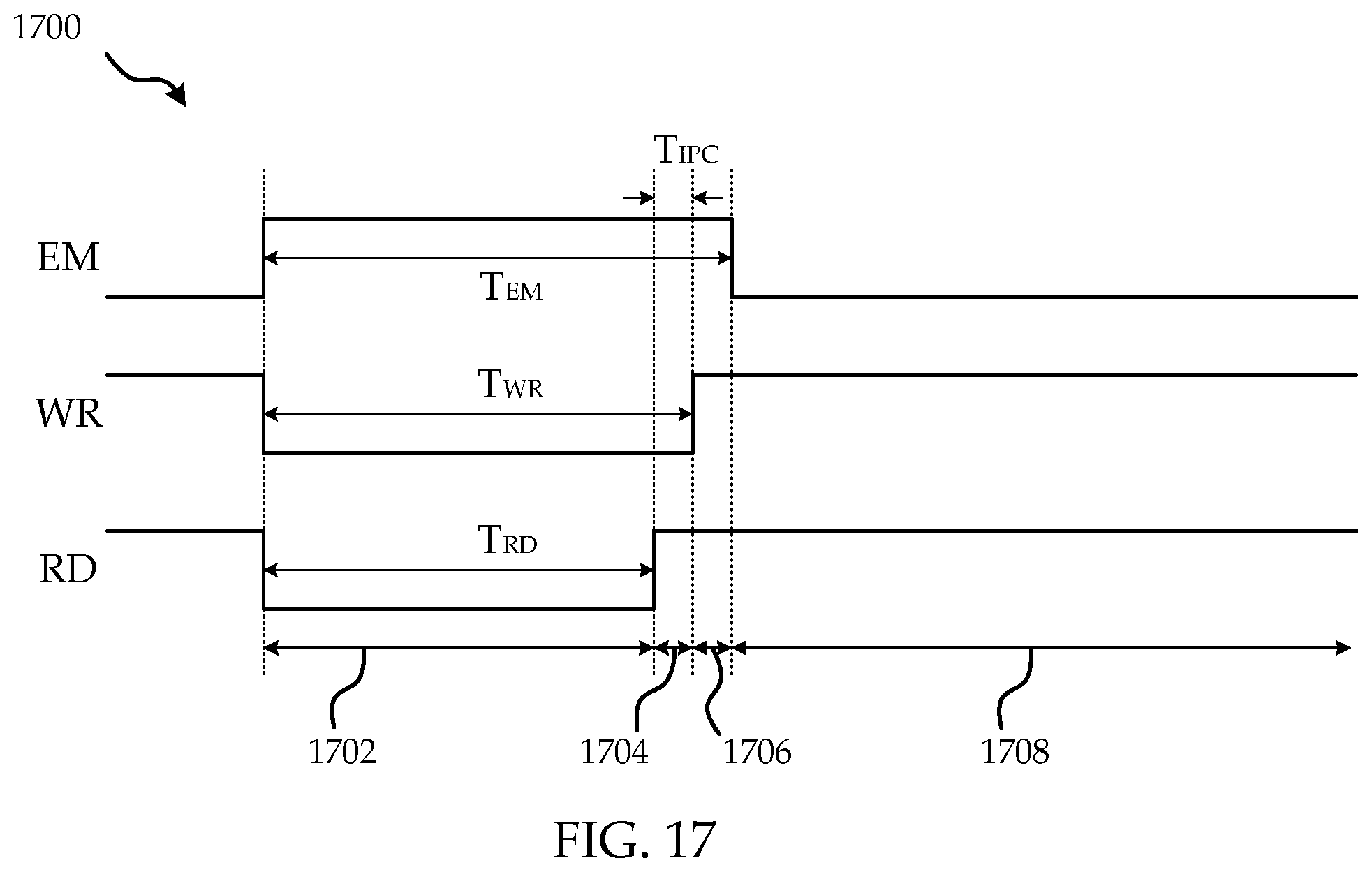
D00018

D00019

D00020

D00021

XML
uspto.report is an independent third-party trademark research tool that is not affiliated, endorsed, or sponsored by the United States Patent and Trademark Office (USPTO) or any other governmental organization. The information provided by uspto.report is based on publicly available data at the time of writing and is intended for informational purposes only.
While we strive to provide accurate and up-to-date information, we do not guarantee the accuracy, completeness, reliability, or suitability of the information displayed on this site. The use of this site is at your own risk. Any reliance you place on such information is therefore strictly at your own risk.
All official trademark data, including owner information, should be verified by visiting the official USPTO website at www.uspto.gov. This site is not intended to replace professional legal advice and should not be used as a substitute for consulting with a legal professional who is knowledgeable about trademark law.