Group III nitride stacked body, and semiconductor device having the stacked body
Kinoshita , et al.
U.S. patent number 10,644,199 [Application Number 16/331,119] was granted by the patent office on 2020-05-05 for group iii nitride stacked body, and semiconductor device having the stacked body. This patent grant is currently assigned to STANLEY ELECTRIC CO., LTD.. The grantee listed for this patent is STANLEY ELECTRIC CO., LTD.. Invention is credited to Toru Kinoshita, Toshiyuki Obata.


| United States Patent | 10,644,199 |
| Kinoshita , et al. | May 5, 2020 |
Group III nitride stacked body, and semiconductor device having the stacked body
Abstract
Provided is a group III nitride stacked body having an n-type Al.sub.XGa.sub.1-XN (0.5.ltoreq.X<1) layer formed on an AlN single crystal substrate while being lattice-matched to the AlN single crystal substrate wherein the n-type Al.sub.XGa.sub.1-XN (0.5.ltoreq.X<1) layer has at least a stacked structure in which a first n-type Al.sub.X1Ga.sub.1-X1N (0.5.ltoreq.X1<1) layer, a second n-type Al.sub.X2Ga.sub.1-X2N (0.5.ltoreq.X2<1) layer, and a third n-type Al.sub.X3Ga.sub.1-X3N (0.5.ltoreq.X3<1) layer are stacked in this order from the AlN single crystal substrate side, and X1, X2, and X3 indicating the Al compositions of the respective layers satisfy 0<|X1-X2|.ltoreq.0.1, and satisfy 0<|X2-X3|.ltoreq.0.1.
| Inventors: | Kinoshita; Toru (Tokyo, JP), Obata; Toshiyuki (Tokyo, JP) | ||||||||||
|---|---|---|---|---|---|---|---|---|---|---|---|
| Applicant: |
|
||||||||||
| Assignee: | STANLEY ELECTRIC CO., LTD.
(Tokyo, JP) |
||||||||||
| Family ID: | 61619110 | ||||||||||
| Appl. No.: | 16/331,119 | ||||||||||
| Filed: | August 28, 2017 | ||||||||||
| PCT Filed: | August 28, 2017 | ||||||||||
| PCT No.: | PCT/JP2017/030706 | ||||||||||
| 371(c)(1),(2),(4) Date: | March 06, 2019 | ||||||||||
| PCT Pub. No.: | WO2018/051772 | ||||||||||
| PCT Pub. Date: | March 22, 2018 |
Prior Publication Data
| Document Identifier | Publication Date | |
|---|---|---|
| US 20190229237 A1 | Jul 25, 2019 | |
Foreign Application Priority Data
| Sep 14, 2016 [JP] | 2016-179114 | |||
| Current U.S. Class: | 1/1 |
| Current CPC Class: | C30B 29/38 (20130101); H01L 33/32 (20130101); C30B 29/403 (20130101); C30B 25/02 (20130101); C30B 25/18 (20130101); H01L 33/0075 (20130101); H01L 33/12 (20130101); C23C 16/34 (20130101); H01L 21/205 (20130101); C30B 25/183 (20130101) |
| Current International Class: | H01L 33/32 (20100101); C30B 29/38 (20060101); C23C 16/34 (20060101); H01L 21/205 (20060101); C30B 25/18 (20060101); H01L 33/00 (20100101); H01L 33/12 (20100101); C30B 25/02 (20060101) |
References Cited [Referenced By]
U.S. Patent Documents
| 6130147 | October 2000 | Major |
| 2008/0187016 | August 2008 | Schowalter et al. |
| 2009/0179221 | July 2009 | Han |
| 2010/0135349 | June 2010 | Schowalter et al. |
| 2013/0292687 | November 2013 | Jiang |
| 2013/0307001 | November 2013 | Lee |
| 2013/0328106 | December 2013 | Kokawa et al. |
| 2015/0200257 | July 2015 | Kim et al. |
| 2017/0110852 | April 2017 | Mino |
| 2017/0201072 | July 2017 | Kotani |
| 2006-351640 | Dec 2006 | JP | |||
| 2010517298 | May 2010 | JP | |||
| 2012243868 | Dec 2012 | JP | |||
| 2015135946 | Jul 2015 | JP | |||
Other References
|
International Search Report (ISR) dated Nov. 7, 2017 issued in International Application No. PCT/JP2017/030706. cited by applicant . Written Opinion dated Nov. 7, 2017 issued in International Application No. PCT/JP2017/030706. cited by applicant . James R. Grandusky, et al., "Properties of Mid-Ultraviolet Light Emitting Diodes Fabricated from Pseudomorphic Layers on Bulk Aluminum Nitride Substrates," Applied Physics Express 3 (2010) 072103, 3 Pages. cited by applicant . James R. Grandusky, et al., "270 nm Pseudomorphic Ultraviolet Light-Emitting Diodes with Over 60 mW Continuous Wave Output Power," Applied Physics Express 6 (2013) 032101, 3 Pages. cited by applicant . James R. Grandusky, et al., "Pseudomorphic growth of thick n-type AlxGa1-xN layers on low-defect-density bulk AIN substrates for UV LED applications," Journal of Crystal Growth 311 (2009), pp. 2864-2866. cited by applicant . Cyril Pernot, et al., "Improved Efficiency of 255-280 nm AlGaN-Based Light-Emitting Diodes," Applied Physics Express 3 (2010) 061004, 3 Pages. cited by applicant. |
Primary Examiner: Sefer; Ahmed N
Attorney, Agent or Firm: Holtz, Holtz & Volek PC
Claims
The invention claimed is:
1. A light emitting device which emits ultraviolet light, comprising: an AlN single crystal substrate; an n-type AlGaN layer formed on said AlN single crystal substrate and lattice matched to said AlN single crystal substrate, said n-type AlGaN layer comprising a first n-type Al.sub.X1Ga.sub.1-X1N (0.5.ltoreq.X1<1) layer, a second n-type Al.sub.X2Ga.sub.1-X2N (0.5.ltoreq.X2<1) layer, and a third n-type Al.sub.X3Ga.sub.1-X3N (0.5.ltoreq.X3<1) layer that are stacked in this order on a surface of said AlN single crystal substrate; an active layer stacked on said n-type AlGaN layer; a p-type AlGaN layer formed on said active layer; and an n-type electrode formed on said third n-type Al.sub.x3Ga.sub.1-x3N layer, wherein X1, X2, and X3 indicating Al compositions of the respective layers satisfy 0<|X1-X2|.ltoreq.0.1, and 0<|X2-X3|.ltoreq.0.1, wherein said n-type electrode is formed at a position where a distance in a depth direction from said n-type electrode to an interface between said first n-type Al.sub.x1Ga.sub.1-x1N layer and said second n-type Al.sub.x2Ga.sub.1-x2N layer is at least 10 nm and less than 150 nm, or at a position where a distance in the depth direction from said n-type electrode to an interface between said second n-type Al.sub.x2Ga.sub.1-x2N layer and said third n-type Al.sub.x3Ga.sub.1-x3N layer is at least 10 nm and less than 150 nm.
2. The light emitting device according to claim 1, wherein said X1, X2, and X3 satisfy X1<X2 and X3<X2, or satisfy X2<X1 and X2<X3.
3. The light emitting device according to claim 1, wherein said X1, X2, and X3 satisfy X1<X2<X3.
4. The light emitting device according to claim 1, wherein a total thickness of said n-type AlGaN layer is at least 500 nm.
5. The light emitting device according to claim 1, having an emission peak wavelength of 210 to 350 nm.
Description
TECHNICAL FIELD
The present invention relates to a novel Group III nitride stacked body applicable to semiconductor devices and the like, and also to a novel ultraviolet light-emitting element having the stacked body.
BACKGROUND ART
Single crystal group III nitride semiconductors represented by the composition formula Al.sub.AGa.sub.1-AN (0.ltoreq.A.ltoreq.1) can freely select the emission peak wavelength in the range of 210 to 365 nm by changing the composition of the group III element (Al, Ga), and have direct transition-type band structures in the energy range corresponding to the above-described wavelength range. Thus, they are optimal materials for forming ultraviolet light-emitting elements.
Ultraviolet light-emitting elements formed of group III nitride semiconductors are generally manufactured by performing crystal-growth of an Al.sub.AGa.sub.1-AN layer on a single crystal substrate by a metal organic chemical vapor deposition method (MOCVD) or a molecular beam epitaxy method (MBE). As a single crystal substrate, materials such as sapphire, SiC (silicon carbide), AlN (aluminum nitride), or the like, which enable epitaxial growth of an Al.sub.AGa.sub.1-AN layer, may be used. Among these, it is known that use of an AlN single crystal substrate which is the same group III nitride as the Al.sub.AGa.sub.1-AN layer can reduce crystal defects (dislocations) formed in the Al.sub.AGa.sub.1-AN layer.
For example, Non-Patent Literatures 1 and 2 disclose that the dislocation density in the Al.sub.AGa.sub.1-AN layer can be reduced by fabricating an ultraviolet light-emitting diode including a stacked structure having an Al.sub.AGa.sub.1-AN layer lattice-matched to, and formed on, an AlN single crystal substrate. Non-Patent Literatures 1 and 2 disclose an ultraviolet light-emitting diode having an emission peak wavelength of 280 nm or less. When a flip-chip type ultraviolet light-emitting element described in these Non-Patent Literatures 1 and 2 is fabricated, it is preferable that the n-type Al.sub.AGa.sub.1-AN layer formed on the AlN single crystal substrate have high conductivity and a large film thickness in order to reduce the driving voltage of the ultraviolet light-emitting element.
Specifically, the film thickness of such an Al.sub.AGa.sub.1-AN-layer has been reported as follows. For example, Non-Patent Literature 3 reports the physical properties of an Al.sub.AGa.sub.1-AN layer formed on an AlN single crystal substrate. Specifically, when the Al.sub.0.6Ga.sub.0.4N layer (Al composition (A) is 0.6) has a film thickness of 0.5 .mu.m or less, and when the Al.sub.0.7Ga.sub.0.3N layer (Al composition (A) is 0.7) has a film thickness of 1.0 .mu.m or less, the lattice constant of the Al.sub.AGa.sub.1-AN layer is maintained to be equal to (lattice-matched to) the lattice constant of the AlN single crystal substrate. Non-Patent Literature 3 also reports that, if this condition is satisfied, Al.sub.AGa.sub.1-AN layers having good surface smoothness and high crystal qualities can be obtained.
In addition, Patent Literature 1 discloses an Al.sub.AGa.sub.1-AN layer which is formed on an AlN single crystal substrate, and whose film thickness is 5 times or more the predicted critical film thickness calculated in accordance with the Matthews-Blakeslee theory (hereinafter, referred to as MB theory in some cases) and whose mean dislocation density is 10.sup.4 cm.sup.-2 or less (Note that Patent Literature 1 describes the unit of the predicted critical film thickness as .ANG. in the drawing showing the relation between the Al composition and the predicted critical film thickness by the MB theory, but it is presumed that it is wrong, and should be nm (nanometer)).
As described above, Non-Patent Literature 3 and Patent Literature 1 disclose relatively thick n-type Al.sub.AGa.sub.1-AN layers formed on, and lattice-matched to, the AlN single crystal substrate.
CITATION LIST
Patent Literature
Patent Literature 1: Japanese Translation of PCT Patent Application Publication No. 2010-517298
Non-Patent Literature
Non-Patent Literature 1: Appl. Phys. Express 3, 072103 (2010) Non-Patent Literature 2: Appl. Phys. Express 6, 032101 (2013) Non-Patent Literature 3: J. Cryst. Growth 311, 2864-2866 (2009) Non-Patent Literature 4: Appl. Phys. Express 3, 061004 (2010)
SUMMARY OF INVENTION
Technical Problem
However, even with the methods described above, there is room for improvement in the following points in order to obtain an ultraviolet light-emitting element having higher performance, specifically, driven with a lower driving voltage.
For example, Non-Patent Literature 4 discloses an ultraviolet light-emitting element having an n-type Al.sub.0.67Ga.sub.0.33N layer of 2 .mu.m on a sapphire substrate. Since the n-type Al.sub.0.67Ga.sub.0.33N layer is formed on the sapphire substrate, the dislocation density is increased. However, since the resistance value in the horizontal (lateral) direction thereof in the n-type Al.sub.AGa.sub.1-AN layer is the reciprocal of the cross-sectional area (product of the width and the film thickness) through which a current flows, the resistance value in the horizontal direction in the n-type Al.sub.0.67Ga.sub.0.33N layer of Non-Patent Literature 4 is, for example, a half or less of that in the n-type Al.sub.0.6Ga.sub.0.4N layer (0.5 .mu.m) and the n-type Al.sub.0.7Ga.sub.0.3N layer (1.0 .mu.m) of Non-Patent Literature 3.
It is considered that the difference in resistance value in the horizontal direction in the n-type Al.sub.AGa.sub.1-AN layer caused by the difference in film thickness is one of the reasons for the higher driving voltage of the ultraviolet light-emitting element fabricated on the AlN substrate. As described above, in the conventional technology, there is room for improvement in the ultraviolet light-emitting element including the AlN single crystal substrate and the n-type Al.sub.AGa.sub.1-AN layer lattice-matched to the AlN single crystal substrate from the viewpoint of lowering a driving voltage.
Accordingly, it is an object of the present invention to provide a group III nitride stacked body having an n-type Al.sub.XGa.sub.1-XN (0.5.ltoreq.X<1) layer lattice-matched to, and formed on, an AlN single crystal substrate, the group III nitride stacked body having high crystal qualities (high crystallinity and low dislocation density) and capable of improving the n-type conductivity in the horizontal direction (capable of being driven with a lower driving voltage).
Solution to Problem
In order to solve the above-described problems, the present inventors have intensively studied structures of n-type Al.sub.XGa.sub.1-XN (0.5.ltoreq.X<1) layers formed on an AlN single crystal substrate. As a result, they have found that, when the n-type Al.sub.XGa.sub.1-XN (0.5.ltoreq.X<1) layer is formed from a plurality of layers of at least three or more layers each having a particular composition differing in Al composition, the n-type Al.sub.XGa.sub.1-XN (0.5.ltoreq.X<1) layer can maintain a state of being lattice-matched to the AlN single crystal substrate, i.e., is capable of improving the conductivity in the horizontal direction while maintaining high crystalline quality, and thus, completed the present invention.
That is, a first aspect of the present invention is a group III nitride stacked body having an n-type Al.sub.XGa.sub.1-XN (0.5.ltoreq.X<1) layer formed on an AlN single crystal substrate while being lattice-matched to the AlN single crystal substrate wherein
the n-type Al.sub.XGa.sub.1-XN (0.5.ltoreq.X<1) layer has at least a stacked structure in which a first n-type Al.sub.X1Ga.sub.1-X1N (0.5.ltoreq.X1<1) layer, a second n-type Al.sub.X2Ga.sub.1-X2N (0.5.ltoreq.X2<1) layer, and a third n-type Al.sub.X3Ga.sub.1-X3N (0.5.ltoreq.X3<1) layer are stacked in this order from the AlN single crystal substrate side, and
X1, X2, and X3 indicating the Al compositions of the respective layers satisfy 0<|X1-X2|.ltoreq.0.1, and satisfy 0<|X2-X3|.ltoreq.0.1.
As described above, X denotes the value of the Al composition (Al composition ratio) in the n-type Al.sub.XGa.sub.1-XN (0.5.ltoreq.X<1) layer. Thus, X satisfies all values of X1, X2, and X3. In addition, X1, X2, and X3 denote values of the Al compositions (Al composition ratios) in the first n-type Al.sub.X1Ga.sub.1-X1N (0.5.ltoreq.X1<1) layer, the second n-type Al.sub.X2Ga.sub.1-X2N (0.5.ltoreq.X2<1) layer, and the third n-type Al.sub.X3Ga.sub.1-X3N (0.5.ltoreq.X3<1) layer, respectively.
Of course, |X1-X2| refers to the absolute value of the difference between X1 and X2, and |X2-X3| refers to the absolute value of the difference between X2 and X3.
In the first aspect of the present invention, in order to further lower the driving voltage, the aforementioned X1, X2, and X3 preferably satisfy X1<X2 and X3<X2, or satisfy X2<X1 and X2<X3, and further preferably satisfy X1<X2<X3.
In the first aspect of the present invention, it is preferable that the film thickness of each layer of the first n-type Al.sub.X1Ga.sub.1-X1N (0.5.ltoreq.X1<1) layer, the second n-type Al.sub.X2Ga.sub.1-X2N (0.5.ltoreq.X2<1) layer, and the third n-type Al.sub.X3Ga.sub.1-X3N (0.5.ltoreq.X3<1) layer be 1 time or more and less than 5 times the predicted critical film thickness. This can achieve a group III nitride stacked body with a higher quality, i.e., a lower dislocation density. Further, in order to facilitate handling of the obtained group III nitride stacked body and further lower the driving voltage, it is preferable that the total thickness of the n-type Al.sub.XGa.sub.1-XN (0.5.ltoreq.X<1) layer be 500 nm or more.
A second aspect of the present invention is a semiconductor device having the group III nitride stacked body according to the first aspect of the present invention, which can be applied to an ultraviolet light-emitting element or the like having an emission peak wavelength of 210 to 350 nm.
Advantageous Effects of the Invention
According to the present invention, there is provided a group III nitride stacked body including an n-type Al.sub.XGa.sub.1-XN (0.5.ltoreq.X<1) layer formed on an AlN single crystal substrate while being lattice-matched to the AlN single crystal substrate, wherein the resistance value of the n-type Al.sub.XGa.sub.1-XN (0.5.ltoreq.X<1) layer in the horizontal direction is reduced. For example, when an ultraviolet light-emitting element (semiconductor device) having an emission peak wavelength of 350 nm or less is fabricated from the group III nitride stacked body, an ultraviolet light-emitting element (semiconductor device) driven with a low driving voltage can be obtained in addition to high emission efficiency and reliability.
BRIEF DESCRIPTION OF DRAWINGS
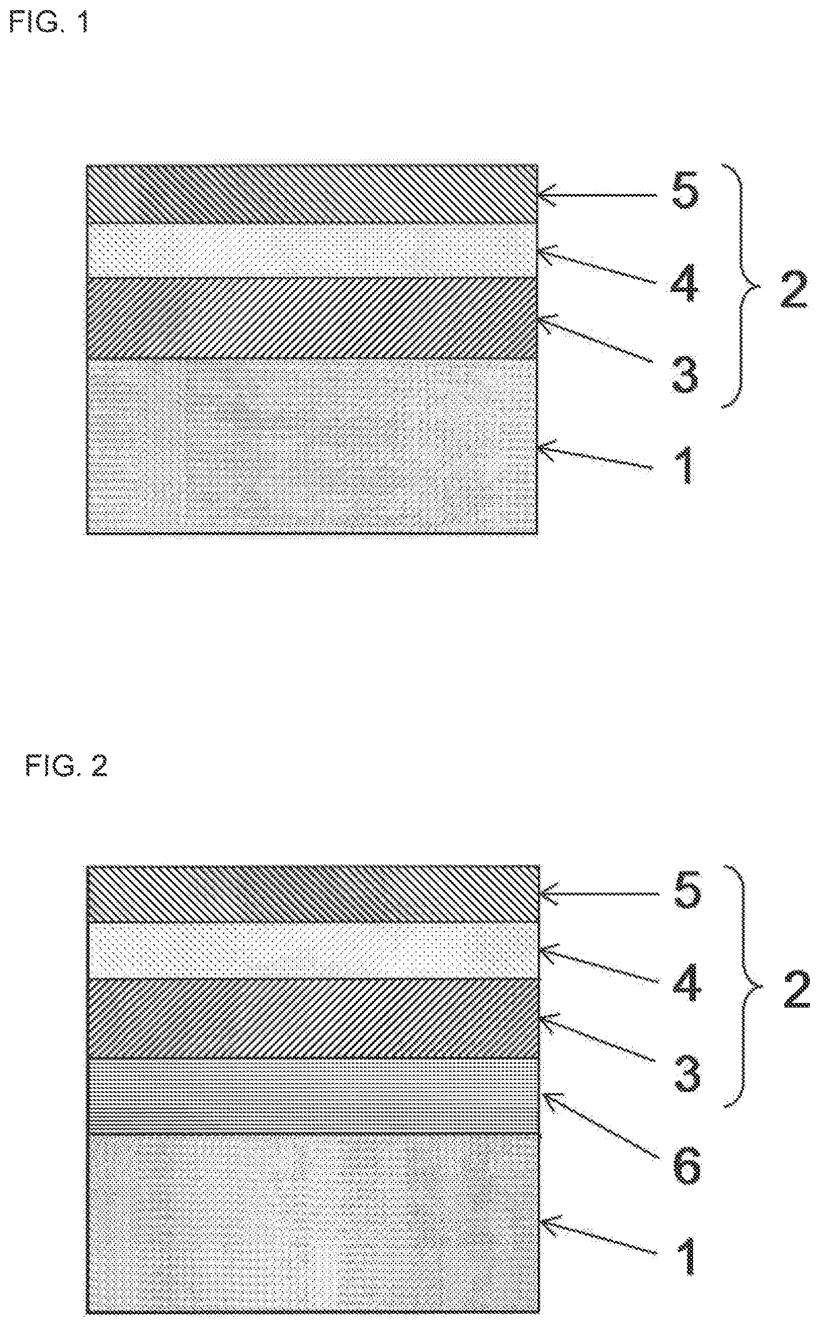
FIG. 1 is a schematic view (schematic cross-sectional view) of an example showing a structure of a group III nitride stacked body of the present invention.
FIG. 2 is a schematic view (schematic cross-sectional view) of another example showing a structure of a group III nitride stacked body of the present invention.
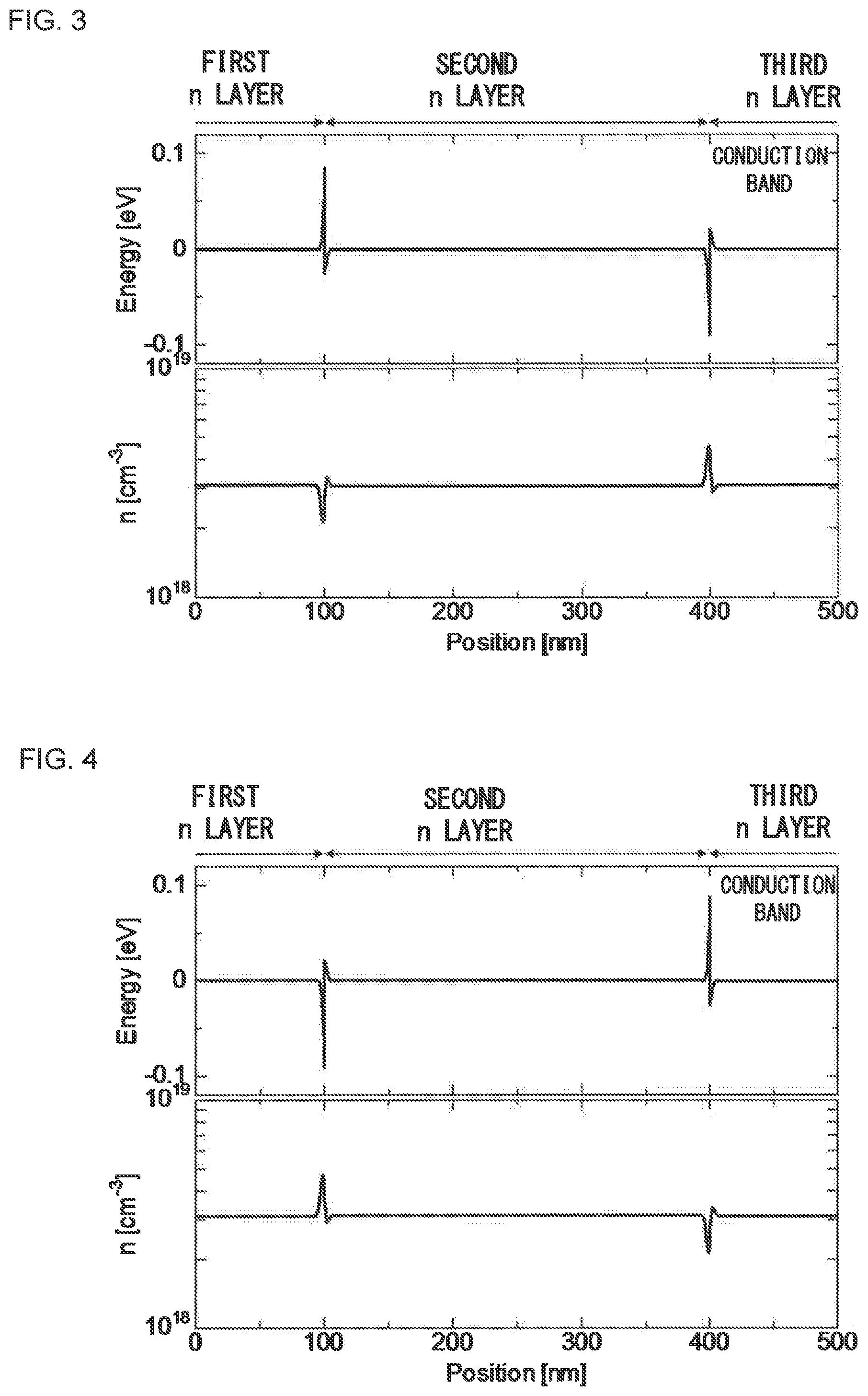
FIG. 3 is a graph showing an energy band and an electron density profile of the group III nitride stacked body of the present invention (which corresponds to Example 1).
FIG. 4 is a graph showing an energy band and an electron density profile of the group III nitride stacked body of the present invention (which corresponds to Example 2).
FIG. 5 is a diagram showing the predicted critical film thickness of the AlGaN layer formed on the AlN substrate according to the MB theory.
FIG. 6 is a schematic view (schematic cross-sectional view) showing an example of a structure of an ultraviolet light-emitting element including the group III nitride stacked body of the present invention.
DESCRIPTION OF EMBODIMENTS
The group III nitride stacked body is a group III nitride stacked body having an AlN single crystal substrate and an n-type Al.sub.XGa.sub.1-XN (0.5.ltoreq.X<1) layer formed on the AlN single crystal substrate while being lattice-matched to the AlN single crystal substrate. Hereinafter, the structure of FIGS. 1 and 2 will be described in order by way of example.
(Group III Nitride Stacked Body)
(AlN Single Crystal Substrate)
In the present invention, the AlN single crystal substrate 1 serving as a base substrate is not particularly limited, but it is preferable to use an AlN single crystal substrate having a low dislocation density. Specifically, the AlN single crystal substrate 1 preferably has a dislocation density of 10.sup.6 cm.sup.-2 or less, and more preferably has a dislocation density of 10.sup.4 cm.sup.-2 or less. Use of the AlN single crystal substrate 1 having a low dislocation density can lower the dislocation density in the n-type Al.sub.XGa.sub.1-XN (0.5.ltoreq.X<1) layer 2, and improve the characteristics of the ultraviolet light-emitting element. The lower limit of the dislocation density is 0 cm.sup.-2. In the present invention, unless otherwise specified, the dislocation density is an etch pit density measured after immersion in a heated acid mixed solution described later.
In the present invention, the crystal growth surface of the AlN single crystal substrate 1, that is, the crystal plane on which the n-type Al.sub.XGa.sub.1-XN (0.5.ltoreq.X<1) layer 2 is grown is not particularly limited as long as the structure of the present invention can be realized. Among these, from the viewpoint of enhancing the smoothness of the n-type Al.sub.XGa.sub.1-XN layer 2, the C-plane is preferable. In addition, the surface may be slightly inclined (off) from the C-plane, and in this case, the off-angle is preferably 0.1 to 0.5.degree., and further preferably inclined in the M-axis direction.
The crystal growth surface of the AlN single crystal substrate 1 is preferably smooth. The smoothness makes it possible to reduce new dislocations generated at the interface with the n-type Al.sub.XGa.sub.1-XN (0.5.ltoreq.X<1) layer 2 stacked on the AlN single crystal substrate 1. Specifically, the root-mean-square roughness (RMS) in the area of 5.times.5 .mu.m.sup.2 is preferably 5 nm or less, more preferably 1 nm or less, and further preferably 0.5 nm or less. Such a smooth surface can be obtained by a known Chemical Mechanical Polish process (CMP polishing). The lower limit value of RMS is preferably 0 nm, but is 0.05 nm in the current technology in consideration of industrial production.
Further, when damage by CMP polishing remains on the crystal growth surface of the AlN single crystal substrate 1, lattice relaxation of the n-type Al.sub.XGa.sub.1-XN (0.5.ltoreq.X<1) layer 2 may occur, and dislocations may newly occur. Therefore, it is necessary to suppress the polishing damage as much as possible. Such polishing damage can be evaluated in the same manner as the measurement of the etch pit density described above. The pits appearing due to the polishing damage are formed in a shape linearly connected to the dislocations and the damage remaining portions in the AlN single crystal substrate 1. Therefore, it is preferable that the density be small. Specifically, it is preferable that the AlN single crystal substrate 1 have a crystal growth surface of 5 pits/mm.sup.2 or less, which is preferably 2 pits/mm.sup.2 or less. As a matter of course, it is necessary to suppress polishing scratches and the like as much as possible, and it is preferable that the number of polishing scratches is 0 pits/substrate.
It is preferable that the AlN single crystal substrate 1 have high transparency to light emitted by a light-emitting element to be finally formed. Therefore, it is preferable that the absorption coefficient in the ultraviolet range, specifically, in wavelengths of 210 nm or more be 25 cm.sup.-1 or less. The lower limit of the absorption coefficient is preferably as low as possible. In particular, in consideration of industrial production of the AlN single crystal substrate 1, measuring accuracy, and the like, the lower limit value of the absorption coefficient at 210 nm is 15 cm.sup.-1, and the lower limit value of the absorption coefficient at the wavelengths of 250 nm or more is 5 cm.sup.-1. Use of the AlN single crystal substrate having such a low absorption coefficient can suppress a decrease in output due to ultraviolet light absorption in the AlN single crystal substrate. Further, it is possible to suppress a decrease in output due to heat generated by absorbing ultraviolet light.
The thickness and size of the AlN single crystal substrate 1 used in the present invention are not particularly limited. If the thickness of the AlN single crystal substrate is small, the amount of light absorption in the substrate can be reduced even when the absorption coefficient is high. However, if the thickness is too thin, the handling of the substrate is difficult and the yield of the light-emitting element may be lowered. Therefore, it is usually preferable that the thickness be 50 to 1000 .mu.m. When the n-type Al.sub.XGa.sub.1-XN (0.5.ltoreq.X<1) layer 2 is grown on the AlN single crystal substrate 1, the larger the size of the AlN single crystal substrate 1 (the area of the crystal growth surface) becomes, the more the number of the light-emitting elements (chips) finally obtained can be increased. However, in consideration of industrial production of the light-emitting element, the size of the AlN single crystal substrate is preferably 0.5 to 6 inches in diameter. As a matter of course, for example, when a light-emitting element (chip) is made, the size of the AlN single crystal substrate portion used in the light-emitting element (chip) is reduced. Therefore, the size of the AlN single crystal substrate portion of the light-emitting element (chip) may be set to a size corresponding to the intended use purpose of the light-emitting element (chip). Usually, in the case of light-emitting elements (chips), the size of the AlN single crystal substrate portion is 0.01 to 10 mm.sup.2 in area.
The AlN single crystal substrate 1 as described above can be fabricated by, for example, the sublimation method or the hydride vapor-phase epitaxial method described in a literature of J. Cryst. Growth 312, 58 to 63 (2009) and a literature of Appl. Phys. Express 5, 055504 (2011). Among these, when the group III nitride stacked body of the present invention is applied to a light-emitting element, it is preferable to fabricate the group III nitride stacked body by the hydride vapor-phase epitaxial method because it has a higher transmittance in the ultraviolet region.
(N-Type Al.sub.XGa.sub.1-XN Layer (0.5.ltoreq.X<1))
In the present invention, the n-type Al.sub.XGa.sub.1-XN (0.5.ltoreq.X<1) layer 2 is a single crystal layer stacked on the AlN single crystal substrate 1. The n-type Al.sub.XGa.sub.1-XN (0.5.ltoreq.X<1) layer 2 formed on the AlN single crystal substrate 1 is lattice-matched to the AlN single crystal substrate 1. Therefore, all the layers constituting the n-type Al.sub.XGa.sub.1-XN layer 2 including the first n-type Al.sub.X1Ga.sub.1-X1N (0.5.ltoreq.X1<1) layer 3, the second n-type Al.sub.X2Ga.sub.1-X2N (0.5.ltoreq.X2<1) layer 4, and the third n-type Al.sub.X3Ga.sub.1-X3N (0.5.ltoreq.X3<1) layer 5 are single crystal layers and lattice-matched to the AlN single crystal substrate 1.
Here, the "lattice matched state" means that the AlN single crystal substrate 1 and the n-type Al.sub.XGa.sub.1-XN (0.5.ltoreq.X<1) layer 2 have substantially the same lattice constants in a direction parallel to the principal surface of the AlN single crystal substrate 1 and the n-type Al.sub.XGa.sub.1-XN (0.5.ltoreq.X<1) layer 2. In other words, in the present invention, the lattice-matched n-type Al.sub.XGa.sub.1-XN (0.5.ltoreq.X<1) layer 2 means that the lattice relaxation rate is 5% or less. The lower limit value of the lattice relaxation rate is 0, which means that the lattice constants of the n-type Al.sub.XGa.sub.1-XN (0.5.ltoreq.X<1) layer 2 and the AlN single crystal substrate 1 coincide with each other. The lattice relaxation rate can be measured by X-ray reciprocal lattice mapping measurement.
The Al composition can be determined by X-ray diffractometry (XRD) or energy-dispersive X-ray spectroscopy (TEM-EDX). In the present invention, Al compositions determined by TEM-EDX were used.
In the present invention, since the n-type Al.sub.XGa.sub.1-XN (0.5.ltoreq.X<1) layer 2 is a single crystal layer and is lattice-matched to the AlN single crystal substrate 1, lattice relaxation of the n-type Al.sub.XGa.sub.1-XN (0.5.ltoreq.X<1) layer 2 accompanied by generation of dislocation does not occur. Therefore, the dislocation density in the n-type Al.sub.XGa.sub.1-XN (0.5.ltoreq.X<1) layer 2 is equivalent to the dislocation density on the surface of the AlN single crystal substrate 1. Therefore, the dislocation density of the n-type Al.sub.XGa.sub.1-XN (0.5.ltoreq.X<1) layer 2 is preferably 10.sup.6 cm.sup.-2 or less as in the case of the AlN single crystal substrate 1, and more preferably 10.sup.4 cm.sup.-2 or less. Although the n-type Al.sub.XGa.sub.1-XN (0.5.ltoreq.X<1) layer 2 of the present invention is formed from a plurality of layers, the dislocation densities of the respective layers do not change because all of these layers are lattice-matched.
The n-type Al.sub.XGa.sub.1-XN (0.5.ltoreq.X<1) layer 2 may be directly stacked on the AlN single crystal substrate 1, or may be stacked via an intermediate layer 6 such as a single crystal AlN layer or an Al.sub.YGa.sub.1-YN (0.5.ltoreq.Y<1) layer as illustrated in FIG. 2. The thickness of the intermediate layer 6 is not particularly limited as long as the n-type Al.sub.XGa.sub.1-XN (0.5.ltoreq.X<1) layer 2 can maintain lattice-matching with the AlN single crystal substrate 1. Usually, from the viewpoint of industrial productivity and the like, the thickness is preferably 10 to 1000 nm. The intermediate layer 6 will be described in detail below.
In the present invention, the n-type Al.sub.XGa.sub.1-XN (0.5.ltoreq.X<1) layer 2 has at least a stacked structure in which the first n-type Al.sub.X1Ga.sub.1-X1N (0.5.ltoreq.X1<1) layer 3, the second n-type Al.sub.X2Ga.sub.1-XN (0.5.ltoreq.X2<1) layer 4, and the third n-type Al.sub.X3Ga.sub.1-X3N (0.5.ltoreq.X<1) layer 5 are stacked in this order from the AlN single crystal substrate side. Then, X1, X2, and X3 representing the Al compositions of the respective layers in the n-type Al.sub.XGa.sub.1-XN (0.5.ltoreq.X<1) layer 2 satisfy 0<|X1-X2|.ltoreq.0.1, and also satisfy 0<|X2-X3|.ltoreq.0.1.
In the present invention, the n-type Al.sub.XGa.sub.1-XN (0.5.ltoreq.X<1) layer 2 only has to have at least a stacked structure in which the first n-type Al.sub.X1Ga.sub.1-X1N (0.5.ltoreq.X1<1) layer 3, the second n-type Al.sub.X2Ga.sub.1-X2N (0.5.ltoreq.X2<1) layer 4, and the third n-type Al.sub.X3Ga.sub.1-X3N (0.5.ltoreq.X3<1) layer 5 are directly stacked in this order. In the present invention, the reason why an excellent effect is exhibited by adopting such a stacked structure is presumed as follows. That is, as in the present invention, providing differences in Al compositions at the respective interfaces of the first, second, and third n-type Al.sub.XGa.sub.1-XN (0.5.ltoreq.X<1) layers forms triangular potentials at the interfaces. As a result, a high electron density layer (a two-dimensional electron gas layer) in which electrons are accumulated at the interface is formed. As a result, it is presumed that the conductivity of the n-type Al.sub.XGa.sub.1-XN (0.5.ltoreq.X<1) layer in the horizontal direction is improved by the electron conduction via the high electron density layer.
In consideration of the mechanism of such an effect, it is considered that the effect of the present invention is exhibited if the first, second, and third n-type Al.sub.XGa.sub.1-XN (0.5.ltoreq.X<1) layers are directly stacked. Therefore, although not shown in FIGS. 1 and 2, an n-type layer composed of another AlGaN may be provided in the lower layer of the first n-type Al.sub.X1Ga.sub.1-X1N (0.5.ltoreq.X1<1) layer 3 and in the upper layer of the third n-type Al.sub.X3Ga.sub.1-X3N (0.5.ltoreq.X3<1) layer 5 in the present invention. When an n-type layer is formed in the lower layer of the first n-type Al.sub.X1Ga.sub.1-X1N (0.5.ltoreq.X<1) layer 3, it can also serve as the intermediate layer 6, which will be described in detail below. However, in consideration of the productivity of the group III nitride stacked body, it is preferable that the n-type Al.sub.XGa.sub.1-XN (0.5.ltoreq.X<1) layer 2 is composed of the first n-type Al.sub.X1Ga.sub.1-X1N (0.5.ltoreq.X1<1) layer 3, the second n-type Al.sub.X2Ga.sub.1-X2N (0.5.ltoreq.X2<1) layer 4, and the third n-type Al.sub.X3Ga.sub.1-X3N (0.5.ltoreq.X3<1) layer 5.
FIGS. 3 and 4 illustrate the energy band and electron density profiles of the n-type Al.sub.XGa.sub.1-XN (0.5.ltoreq.X<1) layer in the group III nitride stacked body of the present invention.
The differences in Al compositions at the interfaces of the first, second, and third n-type Al.sub.XGa.sub.1-XN (0.5.ltoreq.X<1) layers, i.e., |X1-X2| and |X2-X3|, exceed 0 and are 0.1 or less. If this value exceeds 0.1, the effect of accumulating electrons at the interface increases, but on the other hand, the resistance value in the film thickness direction increases because the barrier in the film thickness direction increases. As a result, the conductive paths of the n-type Al.sub.XGa.sub.1-XN (0.5.ltoreq.X<1) layer 2 in the horizontal direction are limited to only the interface, and the resistance value may increase, which is not preferable. When the difference in composition is 0, the effect of the present invention is not exhibited. In consideration of the effects of accumulation of electrons at the interface, it is preferable to satisfy 0.02.ltoreq.|X1-X2|.ltoreq.0.1 and 0.02.ltoreq.|X2-X3|.ltoreq.0.1, and further preferably to satisfy 0.03.ltoreq.|X1-X2|.ltoreq.0.1 and 0.03.ltoreq.|X2-X3|.ltoreq.0.1.
In the n-type Al.sub.XGa.sub.1-XN (0.5.ltoreq.X<1) layer 2, the relationship among the Al compositions of the first, second, and third n-type Al.sub.XGa.sub.1-XN layers is preferably such that the X1, X2, and X3 satisfy X1<X2 and X3<X2, or satisfy X2<X1 and X2<X3. In this case, the Al composition (X2) of the second n-type Al.sub.X2Ga.sub.1-X2N (0.5.ltoreq.X2<1) layer 4 located at the intermediate position is higher or lower than the Al compositions of the other two layers.
As another preferable Al composition relationship, it is preferable to satisfy X1<X2<X3. This means that the Al compositions are gradually increased in the stacked structure in which the first, second, and third n-type Al.sub.XGa.sub.1-XN layers are stacked.
When such a composition relationship is satisfied, a high electron density layer is formed at the interface between the first and second or second and third n-type layers, and good conductivity of the n-type Al.sub.XGa.sub.1-XN (0.5.ltoreq.X<1) layer 2 in the horizontal direction can be obtained.
The film thickness of each layer of the first, second, and third n-type Al.sub.XGa.sub.1-XN (0.5.ltoreq.X<1) layers is preferably 1 time or more and less than 5 times the predicted critical film thickness (see FIG. 5) based on the MB theory.
If the thickness of each layer is less than 5 times the predicted critical film thickness based on the MB theory, the relaxation of the n-type Al.sub.XGa.sub.1-XN (0.5.ltoreq.X<1) layer 2 can be suppressed, that is, the risk of dislocation occurring in the n-type Al.sub.XGa.sub.1-XN (0.5.ltoreq.X<1) layer 2 can be reduced. Therefore, by setting the film thickness of each layer of the first, second, and third n-type Al.sub.XGa.sub.1-XN (0.5.ltoreq.X<1) layers to be 1 time or more and less than 5 times the predicted critical film thickness, it becomes easy to obtain a single crystal layer lattice-matched to the AlN single crystal in the entire n-type Al.sub.XGa.sub.1-XN (0.5.ltoreq.X<1) layer 2.
The lower limit value of the film thickness of each layer is preferably 1 time the predicted critical film thickness based on the MB theory. Since the film thickness of each layer is approximately several tens of nanometers when it is less than 1 time the predicted critical film thickness, manufacturing processes tend to be complicated in order to obtain, for example, a total film thickness for ensuring sufficient conductivity of the n-type Al.sub.XGa.sub.1-XN (0.5.ltoreq.X<1) layer in the ultraviolet light-emitting element.
Therefore, the film thickness of each layer of the first, second, and third n-type Al.sub.XGa.sub.1-XN (0.5.ltoreq.X<1) layers is preferably 2 times or more and less than 5 times, more preferably 3 times or more and less than 5 times, and particularly preferably 3 times or more and 4.9 times or less, the predicted critical film thickness based on the MB theory in consideration of the controllability of the film thickness and the reproducibility of processes.
The total thickness of the n-type Al.sub.XGa.sub.1-XN (0.5.ltoreq.X<1) layer 2 is 500 nm or more. It should be understood that the total thickness of the n-type Al.sub.XGa.sub.1-XN (0.5.ltoreq.X<1) layer 2 is the total thickness of all of the n-type layers including the first n-type Al.sub.X1Ga.sub.1-X1N (0.5.ltoreq.X1<1) layer 3, the second n-type Al.sub.X2Ga.sub.1-X2N (0.5.ltoreq.X2<1) layer 4, and the third n-type Al.sub.X3Ga.sub.1-X3N (0.5.ltoreq.X3<1) layer 5, and, as necessary, n-type layers formed in the lower layer of the first n-type Al.sub.X1Ga.sub.1-X1N (0.5.ltoreq.X1<1) layer 3 and in the upper layer of the third n-type Al.sub.X3Ga.sub.1-X3N (0.5.ltoreq.X<1) layer 5. In consideration of the improvement in conductivity in the horizontal direction, the total thickness is preferably 700 nm or more. When the total thickness is 500 nm or more, the film has a sufficient thickness, so that a decrease in conductivity in the horizontal direction can be suppressed. The upper limit of the total thickness of the n-type Al.sub.XGa.sub.1-XN (0.5.ltoreq.X<1) layers is not particularly limited, but is 3000 nm from the viewpoint of productivity and lattice matching with AlN single crystal substrates.
In the present invention, it is preferable that the n-type Al.sub.XGa.sub.1-XN (0.5.ltoreq.X<1) layer 2 be doped with Si as an n-type dopant. The concentration of the dopant is not particularly limited, and may be appropriately determined depending on the intended purpose. In particular, in order to realize high conductivity, the Si concentration is preferably 1.times.10.sup.18 cm.sup.-3 to 5.times.10.sup.19 cm.sup.-3. As described above, although the n-type Al.sub.XGa.sub.1-XN (0.5.ltoreq.X<1) layer 2 is composed of a plurality of layers, it is preferable that the concentration of Si in each layer be 1.times.10.sup.18 cm.sup.-3 to 5.times.10.sup.19 cm.sup.-3. The Si concentration of each layer may be constant, the Si concentration of each layer may be changed according to the device design or the like, or the Si concentration at the interface of each layer may be increased.
The n-type Al.sub.XGa.sub.1-XN (0.5.ltoreq.X<1) layer 2 preferably has a low carbon impurity content. For example, when a large amount of carbon is mixed into the n-type Al.sub.XGa.sub.1-XN (0.5.ltoreq.X<1) layer 2, the conductivity or transparency may be deteriorated. Thus, the carbon concentration in the n-type Al.sub.XGa.sub.1-XN (0.5.ltoreq.X<1) layer 2 is preferably 10.sup.17 cm.sup.-3 or less, and further preferably 5.times.10.sup.16 cm.sup.-3 or less.
In the present invention, it is preferable that the uppermost surface of the n-type Al.sub.XGa.sub.1-XN (0.5.ltoreq.X<1) layer 2 and the interface between the layers whose Al compositions change be smooth. In particular, since the interface of each layer is smooth in the n-type Al.sub.XGa.sub.1-XN (0.5.ltoreq.X<1) layer, an unintentional increase in the impurity content at the interface can be prevented. More specifically, the root-mean-square roughness (RMS) of the uppermost surface and the respective interfaces in the 5.times.5 .mu.m.sup.2 area is preferably 10 nm or less, more preferably 5 nm or less, and further preferably 1 nm or less. The lower limit value of RMS is preferably 0 nm, but is 0.05 nm by the current technology in consideration of industrial production.
Although hillocks of several micrometers may be formed on the outermost surface of the n-type Al.sub.XGa.sub.1-XN (0.5.ltoreq.X<1) layer 2, such hillocks may cause degradation of the characteristics of the semiconductor devices of the present invention. Therefore, the hillock density of the surface is preferably 10 pieces/mm.sup.2, more preferably 5 pieces/mm.sup.2, and further preferably 1 pieces/mm.sup.2 or less. These hillocks can be controlled by the growth method of the n-type Al.sub.XGa.sub.1-XN (0.5.ltoreq.X<1) layer 2. In the present invention, the hillock density can be measured by surface observation using a Nomarski microscope.
(Growth Method of N-Type Al.sub.XGa.sub.1-XN (0.5.ltoreq.X<1) Layer)
In the present invention, the n-type Al.sub.XGa.sub.1-XN (0.5.ltoreq.X<1) layer 2 described above can be manufactured on an AlN single crystal substrate by a known crystal growth method such as a metal-organic chemical vapor deposition (MOCVD) method or a molecular beam epitaxy (MBE) method. Among these, an MOCVD method having high productivity and industrially used widely is preferable. The n-type Al.sub.XGa.sub.1-XN (0.5.ltoreq.X<1) layer 2 formed by the MOCVD method can be manufactured, for example, with reference to the conditions described in International Publication (WO2012/056928).
As the group III source gas, the group V source gas, and the dopant source gas used in the MOCVD method, known materials that can be used for forming the n-type Al.sub.XGa.sub.1-XN (0.5.ltoreq.X<1) layer 2 can be used without any particular limitation.
For example, as the group III source gas, it is preferable to use a gas such as trimethylaluminum, triethylaluminum, trimethylgallium, triethylgallium, or the like. As the group V source gas, ammonia is preferably used. As the n-type doping source gas, a silane-based gas such as monosilane or tetraethylsilane is preferably used. As the n-type doping source gas, the group III source gas and the group V source gas only have to be supplied simultaneously.
The above-described source gas is supplied to a reactor together with a carrier gas such as hydrogen and/or nitrogen to grow the n-type Al.sub.XGa.sub.1-XN (0.5.ltoreq.X<1) layer 2 on the AlN single crystal substrate 1. The preferable range of the molar ratio (V/III ratio) of the group V source gas and the group III source gas is not particularly limited, but is preferably set within the range of 500 to 10000. The V/III ratio only has to be appropriately determined within the above-mentioned set range.
The growth temperatures and the growth pressures of the n-type Al.sub.XGa.sub.1-XN (0.5.ltoreq.X<1) layer 2 are not particularly limited, but are preferably in the range of 1000 to 1300.degree. C. and in the range of 30 to 1000 mbar, respectively, and more preferably in the range of 1030 to 1130.degree. C. and in the range of 30 to 500 mbar, respectively.
In the n-type Al.sub.XGa.sub.1-XN (0.5.ltoreq.X<1) layer 2, when the composition of each layer is changed, the ratio of the group III source gas to be supplied, for example, the supply ratio of trimethylaluminum and trimethylgallium only has to be changed, whereby a plurality of layers having different Al composition (X) values can be stacked. In order to form a stacked structure in which the first n-type Al.sub.X1Ga.sub.1-X1N (0.5.ltoreq.X1<1) layer 3, the second n-type Al.sub.X2Ga.sub.1-X2N (0.5.ltoreq.X2<1) layer 4, and the third n-type Al.sub.X3Ga.sub.1-X3N (0.5.ltoreq.X3<1) layer 5 are directly stacked in this order, a group III source gas only has to be supplied so as to satisfy the Al compositions (X1, X2, and X3) of the respective layers. When the Si concentration is changed in each layer, a layer having a different Si concentration can be fabricated by changing the supply ratio of the n-type doping source gas to the group III source gas.
The n-type Al.sub.XGa.sub.1-XN (0.5.ltoreq.X<1) layer 2 stacked on the AlN single crystal layer 1 has been described above (the group III nitride stacked body of the present invention and the manufacturing method thereof have been described). Next, a preferred example of a (ultraviolet) light-emitting element (semiconductor device) having the structure of the group III nitride stacked body will be described.
(Light-Emitting Element with Preferred Structure: Semiconductor Device)
When an ultraviolet light-emitting element including the group III nitride stacked body of the present invention is manufactured, it is preferable to fabricate a stacked structure composed of a plurality of Al.sub.ZGa.sub.1-ZN (0.ltoreq.Z.ltoreq.1) layers in which the active layer 7 and the p-type layer 9 are stacked in this order on the group III nitride stacked body of the present invention (see FIG. 6). As illustrated in FIG. 2, the intermediate layer 6 formed of a single crystal may be provided between the AlN single crystal substrate 1 and the n-type Al.sub.XGa.sub.1-XN (0.5.ltoreq.X<1) layer 2. Next, a semiconductor device will be described with reference to FIG. 6.
The active layer 7 and the p-type layer 9 described above may be a single layer, but each may be a plurality of layers, for example, layers having different Al compositions or layers having different dopant concentrations. For example, the electron-blocking layer 8 having a high Al composition can be formed between the active layer 7 and the p-type layer 9. The electron-blocking layer 8 may be the p-type layer 9. A contact layer 10 formed of p-type GaN may also be provided on the p-type layer 9 in order to improve the contact characteristics with the electrode. These layers will be described.
(Intermediate Layer 6)
The intermediate layer 6 is directly stacked on the AlN single crystal substrate 1, and is formed of a single crystal AlN layer or an Al.sub.YGa.sub.1-YN (0.5.ltoreq.Y<1) layer, and can be used for the intended purpose of reducing the hillock density on the surface of the n-type Al.sub.XGa.sub.1-XN (0.5.ltoreq.X<1) layer 2, suppressing the occurrence of lattice relaxation of the n-type Al.sub.XGa.sub.1-XN (0.5.ltoreq.X<1) layer 2, or the like. The intermediate layer 6 may be an undoped layer containing no impurities or a doped layer containing impurities such as Si or Mg within a range in which the crystalline quality of the n-type Al.sub.XGa.sub.1-XN (0.5.ltoreq.X<1) layer 2 is maintained. When such an intermediate layer 6 is provided, the thickness thereof is preferably 10 to 1000 nm. However, when Si is contained, the intermediate layer 6 can be regarded as a part of the n-type Al.sub.XGa.sub.1-XN (0.5.ltoreq.X<1) layer.
The intermediate layer 6 is preferably manufactured by the MOCVD method described in the growth method of the n-type Al.sub.XGa.sub.1-XN (0.5.ltoreq.X<1) layer 2. As other growth conditions, the range described in the growth method of the n-type Al.sub.XGa.sub.1-XN (0.5.ltoreq.X<1) layer 2 may be adopted. The intermediate layer 6 is not an essential layer, and is provided between the AlN single crystal substrate 1 and the n-type Al.sub.XGa.sub.1-XN (0.5.ltoreq.X<1) layer 2 as necessary.
<N-Type Al.sub.XGa.sub.1-XN (0.5.ltoreq.X<1) Layer 2>
When the n-type Al.sub.XGa.sub.1-XN (0.5.ltoreq.X<1) layer 2 is applied to an ultraviolet light-emitting element in the present invention, the configurations of the respective layers, the compositions (X1, X2, and X3), the film thicknesses of the respective layers, and the like may be determined in accordance with the wavelengths of the target ultraviolet light-emitting element within the range of the n-type Al.sub.XGa.sub.1-XN (0.5.ltoreq.X<1) layer 2 in the group III nitride stacked body which has been described. The details are as mentioned above.
<Active Layer 7>
The active layer 7 is stacked on the uppermost surface of the n-type Al.sub.XGa.sub.1-XN (0.5.ltoreq.X<1) layer 2. In the present invention, it is particularly preferable that the active layer 7 be formed on the third n-type Al.sub.X3Ga.sub.1-X3N (0.5.ltoreq.X3<1) layer 5. The active layer 7 is preferably an AlGaN layer lattice-matched to the AlN-single crystal substrate 1. For the active layer 7, a known structure such as a multiple quantum well layer in which a well layer and a barrier layer are stacked a plurality of times may be used without limitation. In addition, Si may be doped into the multiple quantum well layer. The compositions of the well layer and the barrier layer may be appropriately determined according to the intended use purpose. Specifically, the Al composition is preferably adjusted in the range of 0.1 to 0.8. The thicknesses of the well layer and the barrier layer are not particularly limited, and usually, the thickness of one well layer is 2 to 10 nm and the thickness of one barrier layer is 5 to 25 nm.
The active layer 7 is also preferably manufactured by the MOCVD method, and the growth conditions may be adjusted as appropriate by employing the range described in the growth method of the n-type Al.sub.XGa.sub.1-XN (0.5.ltoreq.X<1) layer so that the active layer 7 has a desired composition.
<Electron-Blocking Layer 8>
The electron-blocking layer 8 is an AlGaN layer stacked on the active layer 7. However, since the electron-blocking layer 8 may be p-type, it can also be regarded as a kind of the p-type layer 9. Since the electron-blocking layer 8 is desired to have a high band gap energy, it is preferable that the Al composition be higher than those of other layers. Therefore, when a light-emitting element having an emission wavelength shorter than 280 nm is particularly fabricated, it is most preferable to use an AlN layer. When the emission wavelength is longer than 280 nm, the Al composition may be appropriately determined within the range of 0.3 to 0.9. The thickness of the electron-blocking layer 8 is not particularly limited, but is 5 to 20 nm.
While the Mg concentration in the electron-blocking layer 8 is not particularly limited, the Mg concentration is preferably 3.times.10.sup.19 to 2.times.10.sup.20 cm.sup.-3, and more preferably 5.times.10.sup.19 to 1.times.10.sup.20 cm.sup.-3.
Preferably, the electron-blocking layer 8 is also manufactured by the MOCVD method. The growth conditions may be adjusted as appropriate by employing the range described in the growth method of the n-type Al.sub.XGa.sub.1-XN (0.5.ltoreq.X<1) layer 2 so that the electron-blocking layer 8 has a desired composition. When Mg is doped, a known Mg dopant gas may be used instead of the Si dopant gas.
<P-Type Layer 9>
The p-type layer 9 is a p-type AlGaN layer formed on the electron-blocking layer 8. The p-type layer 9 may be formed from a plurality of layers, but may also be stacked on the active layer 7 because it provides the same function as the electron-blocking layer 8 if there is a layer whose Al composition is higher than those of the other layers. The composition of the p-type layer 9 may be appropriately determined depending on the intended use purpose, and in particular, when a light-emitting element having an emission wavelength shorter than 280 nm is to be fabricated, the Al composition is preferably adjusted in the range of 0.7 to 1.0. The thickness of the p-type layer 9 is not particularly limited, and is usually about 5 to 100 nm. Further, the Mg concentration in the p-type layer 9 is not particularly limited similarly to the electron-blocking layer 8, but the Mg concentration is preferably 3.times.10.sup.19 to 2.times.10.sup.20 cm.sup.-3, and more preferably 5.times.10.sup.19 to 1.times.10.sup.20 cm.sup.-3.
The p-type layer 9 is also preferably manufactured by the MOCVD method, and the growth conditions may be adjusted as appropriate by employing the range described in the growth method of the n-type Al.sub.XGa.sub.1-XN (0.5.ltoreq.X<1) layer 2 so that the p-type layer 9 has a desired composition. It should be understood that a known Mg dopant gas is used instead of the Si dopant gas.
<Contact Layer (p-Type GaN Layer) 10>
A contact layer 10 may be provided on the p-type layer 9. The contact layer 10 is preferably a p-type GaN layer. By providing the contact layer 10, the contact resistance with the electrode electrically connected to the p-type layer 9 can be reduced as described above. The film thickness of the p-type GaN layer is not particularly limited, but may be appropriately determined in the range of 5 to 1000 nm. The Mg concentration in the p-type GaN layer is not particularly limited, but the Mg concentration in the p-type GaN layer is preferably 1.times.10.sup.19 to 2.times.10.sup.20 cm.sup.-3, and more preferably 5.times.10.sup.19 to 1.times.10.sup.20 cm.sup.-3.
The contact layer 10 is also preferably manufactured by the MOCVD method, and the other growth conditions may be adjusted as appropriate on the basis of the growth conditions described in Japanese Patent No. 5401145 so as to obtain desired characteristics. It should be understood that a known Mg dopant gas is used instead of the Si dopant gas.
<N-Type Electrode 12>
The n-type electrode 12 is formed on the n-type Al.sub.XGa.sub.1-XN (0.5.ltoreq.X<1) layer 2 exposed by etching or the like. Usually, the n-type electrode 12 is formed on the n-type Al.sub.XGa.sub.1-XN (0.5.ltoreq.X<1) layer 2 by the following method. Among these, it is preferable to form the n-type electrode 12 at a position where the distance in the depth direction between the n-type electrode 12 and the interface between the first and second, or second and third n-type Al.sub.XGa.sub.1-XN (0.5.ltoreq.X<1) layers is 10 nm or more and 150 nm or less, and more preferably 20 nm or more and 100 nm or less. This facilitates accessing the high-density electron layer from the n-electrode 12, and in addition to improving the conductivity of the n-type Al.sub.XGa.sub.1-XN (0.5.ltoreq.X<1) layer 2 in the horizontal direction, the contact resistance of the n-electrode 12 and the n-type Al.sub.XGa.sub.1-XN (0.5.ltoreq.X<1) layer 2 can be reduced.
For the n-type electrode 12, known n-type ohmic electrode materials and forming methods may be used. Specifically, there is no particular limitation imposed thereon as long as the material can reduce the contact resistance value with the n-type Al.sub.XGa.sub.1-XN (0.5.ltoreq.X<1) layer 2. Specifically, it is preferable to use the electrode material containing Ti and Al described in Japanese Patent Application Laid-Open No. 2011-547604.
These electrode materials can be formed by a vacuum evaporation method, a sputtering method, or the like. In order to reduce the contact resistance value, annealing is preferably performed in an inert gas atmosphere such as argon or nitrogen after the electrode layer is formed. The annealing temperature is not particularly limited, but is preferably 700 to 1100.degree. C. The thickness of the n-type electrode (layer) 12 is not particularly limited, and the film thickness of each layer may be appropriately determined within a range in which the contact resistance value after annealing can be reduced, but the total thickness is preferably 50 to 500 nm in consideration of the productivity and the like of the electrode layer.
(P-Type Electrode 11)
As the p-type electrode (layer) 11, a known p-type ohmic electrode material can be used. Specifically, there is no particular limitation imposed thereon as long as the material can reduce the contact resistance value with the contact layer 10, and for example, an electrode material containing Ni and Au described in Japanese Patent No. 3499385 can be used.
These electrode materials can be formed by a vacuum evaporation method, a sputtering method, or the like. After the p-type electrode is formed, annealing treatment is preferably performed in an atmosphere of nitrogen, oxygen, or the like in order to reduce the contact resistance value. The annealing temperature is not particularly limited, but is generally about 400 to 700.degree. C. Although not particularly limited, the thickness of the p-electrode 11 is preferably 5 to 300 nm.
(Characteristics of Light-Emitting Element; Characteristics of Semiconductor Device)
The semiconductor device of the present invention can be an ultraviolet light-emitting element having an emission peak wavelength of 210 to 350 nm by preparing the compositions and the like of the respective layers. An ultraviolet light-emitting element having an emission peak wavelength in this range must have a configuration in which the Al composition is relatively high. Therefore, the group III nitride stacked body of the present invention can be suitably applied thereto.
EXAMPLES
Hereinafter, the present invention will be described in detail using an example in which the present invention is applied to a light-emitting diode having a structure illustrated in FIG. 6 and having an emission wavelength band of 260 nm, but the present invention is not limited to the following examples.
Example 1
(Preparation of AlN Single Crystal Substrate 1)
An AlN single crystal substrate was fabricated by the method described in Applied Physics Express 5 (2012) 122101. Specifically, a C-plane AlN seed substrate having a diameter of 25 mm fabricated by a PVT method was first prepared. The AlN seed substrate has an off-angle of 0.05 to 0.5.degree. and a dislocation density of 10.sup.4 cm.sup.-2 or less. Further, when X-ray rocking curves of the (002) and (101) planes were measured under the condition of an acceleration voltage of 45 kV and an acceleration current of 40 mA by a high-resolution X-ray diffractometer (X'Pert manufactured by the PANalytical Division of Spectris), the full width at half maximum of the X-ray rocking curve was 30 arcsec or less.
Next, an AlN thick film (hereinafter referred to as an AlN thick film by the HVPE method) with a thickness of 300 .mu.m was formed on the AlN seed substrate by the HVPE method. After that, chemical mechanical polishing (CMP) was performed on the AlN thick film grown surface thereof. It was confirmed that the full width at half maximum of the X-ray rocking curve of the AlN thick film by the HVPE method after CMP-polishing was 30 arcsec or less equivalent to that of the AlN seed substrate, and the dislocation density of the AlN thick film by the HVPE method was also confirmed to maintain a crystal quality of 10.sup.4 cm.sup.-2 or less as in the case of the AlN seed substrate.
The off-angle of the AlN thick film by the HVPE method after CMP-polishing was controlled to be 0.2 to 0.5.degree.. The surface roughness (RMS) of the crystal growth surface (polished surface of the AlN thick film by the HVPE method) of the growth substrate (substrate in which the AlN thick film by the HVPE method was stacked on the AlN seed substrate) fabricated in this manner was 0.1 nm or less in the range of 5.times.5 .mu.m.sup.2, and the etch pit density confirmed by a Nomarski microscope after immersion in an acid mixed solution (sulfuric acid:phosphoric acid=1:3) at 190.degree. C. for 10 minutes was 4.times.10.sup.4/cm.sup.2.
Further, as a result of measuring the transmittance of the AlN thick film by the HVPE method fabricated in the same manner, it was confirmed that the linear transmittance of 260 nm was 60% or more and the absorbing coefficient in the same wavelength range was 10 cm.sup.-1 or less. As will be described in detail below, the AlN seed substrate portion is finally removed from the growth substrate when the ultraviolet light-emitting element is fabricated. Therefore, the AlN single crystal substrate in the present invention corresponds to the AlN thick film portion by the HVPE method.
A light-emitting element (semiconductor device) having the structure shown in FIG. 6 was fabricated using the growth substrate (AlN single crystal substrate) fabricated as described above. First, a growth substrate was placed on a susceptor in an MOCVD apparatus, and the substrate was heated to 1200.degree. C. while a mixed gas of hydrogen and nitrogen was caused to flow at a total flow rate of 13 slm to clean the crystal growth surface.
(Formation of N-Type Al.sub.XGa.sub.1-XN (0.5.ltoreq.X<1) Layer 2)
(Formation of First N-Type Al.sub.X1Ga.sub.1-X1N (0.5.ltoreq.X1<1) Layer 3)
Next, an n-type Al.sub.0.7Ga.sub.0.3N layer (first n-type AlGaN layer 3, X1=0.70) was formed to have a thickness of 250 nm (4.4 times the expected critical film thickness) under the following conditions: the substrate temperature was 1050.degree. C.; the flow rate of trimethylaluminum was 35 .mu.mol/min; the flow rate of trimethylgallium was 18 .mu.mol/min; the flow rate of tetraethylsilane was 0.02 .mu.mol/min; and the flow rate of ammonia was 1.5 slm.
(Formation of Second N-Type Al.sub.X2Ga.sub.1-X2N (0.5.ltoreq.X2<1) Layer 4)
Next, an n-type Al.sub.0.66Ga.sub.0.34N layer (second n-type AlGaN layer 4, X2=0.66) was formed to have a thickness of 200 nm (4.0 times the expected critical film thickness) under the same conditions as those for the first n-type AlGaN layer except that the flow rate of trimethylgallium was 22 .mu.mol/min.
(Formation of Third N-Type Al.sub.X2Ga.sub.1-X2N (0.5.ltoreq.X2<1) Layer 5)
Next, an n-type Al.sub.0.73Ga.sub.0.27N layer (third n-type AlGaN layer 5, X3=0.73) was formed to have a thickness of 250 nm (3.7 times the expected critical film thickness) under the same conditions as those for the first n-type AlGaN layer except that the flow rate of trimethylgallium was 16 .mu.mol/min.
(Formation of Active Layer 7)
Next, a barrier layer was formed to have a thickness of 10 nm under the same conditions as those for the n-type Al.sub.0.7Ga.sub.0.3N layer except that the flow rate of tetraethylsilane was 0.002 .mu.mol/min. Next, an Al.sub.0.5Ga.sub.0.5N well layer was formed to have a thickness of 3 nm under the same conditions as those for the barrier layer except that the flow rate of trimethylgallium was 40 .mu.mol/min, the flow rate of trimethylaluminum was 3 .mu.mol/min, and the flow rate of tetraethylsilane was 0 .mu.mol/min. By repeating the growth of the well layer and the barrier layer three times, a triple quantum well layer (active layer 7) was formed.
(Electron-Blocking Layer 8)
Next, a p-type AlN layer 8 (electron-blocking layer 8) was formed to have a thickness of 20 nm under the same conditions as those for the first n-type AlGaN layer 3 except that the supply of trimethylgallium and tetraethylsilane was stopped, and bicyclopentadienylmagnesium was supplied at 1.0 .mu.mol/min.
(p-Type Layer 9)
Next, a p-type Al.sub.0.9Ga.sub.0.2N layer 9 (p-type layer 9) was formed to have a thickness of 50 nm under the same conditions as those for the p-type AlN layer 8 (electron-blocking layer 8) except that the flow rate of trimethylgallium supplied was 8 .mu.mol/min.
(Contact Layer 10)
Next, a contact layer 10 (p-type GaN layer 10) was formed to have a thickness of 300 nm under the conditions such that, after the substrate temperature was changed to 1030.degree. C. and the pressure was changed to 200 mbar, the flow rate of trimethylgallium was 0.2 .mu.mol/min, the flow rate of ammonia was 3.0 slm, the flow rate of bicyclopentadienylmagnesium was 1.0 .mu.mol/min, and the flow rate of a carrier gas was 7 slm.
(Confirmation of Physical Properties of Group III Nitride Stacked Body)
Further, the crystal qualities of the respective layers (n-type Al.sub.XGa.sub.1-XN layer to p-type GaN layer) fabricated as described above were evaluated by a high-resolution X-ray diffractometer in the same manner as that for the AlN single crystal substrate. As a result of XRD-reciprocal lattice mapping measurements on the (114) plane for evaluating the states of lattice relaxation of the respective layers, it was confirmed that the lattice relaxation rates of the respective layers of the n-type Al.sub.XGa.sub.1-XN layer (0.5.ltoreq.X<1) were all 0.5% or less and lattice-matched with the AlN single crystal substrates. In other words, it was confirmed that all the layers in the n-type Al.sub.XGa.sub.1-XN layer 2 were lattice-matched.
(Formation of N-Electrode 12)
Next, a part of the substrate was etched by an ICP-etching apparatus until the n-type Al.sub.0.73Ga.sub.0.27N layer (third n-type AlGaN layer 5) was exposed. The remaining thickness of the n-type Al.sub.0.73Ga.sub.0.27N layer 5 (third n-type AlGaN layer 5) confirmed by measuring the step after the etching was 50 nm. Next, a Ti (20 nm)/Al (100 nm)/Ti (20 nm)/Au (50 nm) electrode 12 was formed on the exposed surface by a vacuum evaporation method, and heat treatment was performed in a nitrogen atmosphere for 1 minute at 900.degree. C.
(Formation of P-Electrode 11)
Next, a Ni (20 nm)/Au (100 nm) electrode 11 was formed on the contact layer 10 (p-type GaN layer 10) by a vacuum evaporation method, and heat treatment was performed in an oxygen atmosphere for 5 minutes at 500.degree. C.
(Semiconductor Device; Fabrication of Ultraviolet Light-Emitting Element)
Next, the AlN seed substrate portion was removed by mechanical polishing until the AlN thick film portion by the HVPE method was exposed, thereby completing the ultraviolet light-emitting element (wafer) (in this case, the AlN thick film portion by the HVPE method corresponds to the AlN single crystal substrate 1). At this time, the thickness of the AlN thick film portion by the HVPE method (the AlN single crystal substrate 1) was 100 .mu.m. As a result of measuring the current and voltage between the p-type and n-type electrodes of each device (each device size was 1.times.1 mm, 300 pieces/1 wafer) of the fabricated ultraviolet light-emitting element (wafer), the average driving voltage at the driving current of 400 mA was 7.9 V.
Next, after the respective devices were cut into a plurality of 1.times.1 mm chip shapes by dicing, they each are flip-chip bonded on a ceramic mount to complete a light-emitting diode. The emission wavelength of the fabricated light-emitting diode was 264 nm, and the light emission output at a driving current of 400 mA was 52 mW. The results are summarized in Table 1.
Example 2
A semiconductor device (ultraviolet light-emitting element) was fabricated in the same manner as in Example 1 except that, in the second n-type Al.sub.X2Ga.sub.1-X2N (0.5.ltoreq.X2<1) layer 4 of Example 1, the flow rate of trimethylgallium was changed to 8 .mu.mol/min, and an n-type Al.sub.0.8Ga.sub.0.2N layer (second n-type AlGaN layer 4, X2=0.8) was formed to have a thickness of 200 nm (2.2 times the expected critical film thickness). As a result of XRD-reciprocal lattice mapping measurements on the (114) plane in confirming the physical properties of the group III nitride stacked body, the lattice relaxation rate of all the layers of the n-type Al.sub.XGa.sub.1-XN (0.5.ltoreq.X<1) layer was 0.5% or less.
The average driving voltage of each device of the fabricated light-emitting diode wafer was 8.0 V. The emission wavelength of the light-emitting diode flip-chip bonded on the ceramic mount was 263 nm, and the light emission output at a driving current of 400 mA was 52 mW. The results are summarized in Table 1.
Example 3
A semiconductor device (ultraviolet light-emitting element) was fabricated in the same manner as that in Example 1 except that the first n-type AlGaN layer 3 (X1=0.7, 250 nm) and the second n-type AlGaN layer 4 (X2=0.66, 200 nm) of the n-type Al.sub.XGa.sub.1-XN (0.5.ltoreq.X<1) layer 2 of Example 1 were replaced with each other. As a result of XRD-reciprocal lattice mapping measurements on the (114) plane in confirming the physical properties of the group III nitride stacked body, the lattice relaxation rate of all the layers of the n-type Al.sub.XGa.sub.1-XN (0.5.ltoreq.X<1) layer was 0.5% or less.
The average driving voltage of each device of the fabricated light-emitting diode wafer was 7.7 V. The emission wavelength of the light-emitting diode flip-chip bonded on the ceramic mount was 264 nm, and the light emission output at a driving current of 400 mA was 53 mW. The results are summarized in Table 1.
Comparative Example 1
A semiconductor device (ultraviolet light-emitting element) was fabricated in the same manner as that in Example 1 except that, in the formation of the n-type Al.sub.XGa.sub.1-XN (0.5.ltoreq.X<1) layer 2 of Example 1, the first n-type Al.sub.X1Ga.sub.1-X1N (0.5.ltoreq.X<1) layer 3 was formed to have a thickness of 700 nm (12.3 times the expected critical film thickness), the second n-type Al.sub.X2Ga.sub.1-X2N layer 4 and the third n-type Al.sub.X3Ga.sub.1-X3N layer 5 was not formed.
As a result of XRD-reciprocal lattice mapping measurements on the (114) plane in confirming the physical properties of the group III nitride stacked body, the relaxation rate of the n-type Al.sub.0.7Ga.sub.0.3N layer (0.7 .mu.m) was 0.5% or less.
The average driving voltage of each device of the fabricated light-emitting diode wafer was 8.8 V. The emission wavelength of the light-emitting diode flip-chip bonded on the ceramic mount was 263 nm, and the light emission output at a driving current of 400 mA was 51 mW. The results are summarized in Table 1.
TABLE-US-00001 TABLE 1 Example Example Example Comparative 1 2 3 Example First n-type Al.sub.X1Ga1.sub.-X1N layer Al Composition (X1) 0.70 0.70 0.66 0.70 Film Thickness (nm) 250 250 200 700 Ratio to Predicted 4.4 4.4 4.0 12.3 Critical Film Thickness Second n-type Al.sub.X2Ga.sub.1-X2N layer No data Al Composition (X2) 0.66 0.80 0.70 -- Film Thickness (nm) 200 200 250 -- Ratio to Predicted 4.0 2.2 4.4 -- Critical Film Thickness Third n-type Al.sub.X3Ga.sub.1-X3N layer No data Al Composition (X3) 0.73 0.73 0.73 -- Film Thickness (nm) 250 250 250 -- Ratio to Predicted 3.7 3.7 3.7 -- Critical Film Thickness | X1 - X2 | 0.04 0.10 0.04 -- | X2 - X3 | 0.07 0.07 0.03 -- Total Film Thickness of 700 700 700 700 n-type AlXGa1-XN layer (nm) Lattice Relaxation Rate up to up to up to up to (%) 0.5% 0.5% 0.5% 0.5% Emission Peak 264 263 264 263 Wavelength (nm) Average Driving 7.9 8.0 7.7 8.8 Voltage (V) Light Emission Output 52 52 53 51 (mW)
REFERENCE SIGNS LIST
1 AlN single crystal substrate 2 n-type Al.sub.XGa.sub.1-XN layer 3 first n-type Al.sub.X1Ga.sub.1-X1N layer 4 second n-type Al.sub.X2Ga.sub.1-X2N layer 5 third n-type Al.sub.X3Ga.sub.1-X3N layer 6 intermediate layer 7 active layer 8 electron-blocking layer 9 p-type layer 10 p-type GaN layer 11 p-type electrode
* * * * *
D00000
D00001
D00002
D00003
XML
uspto.report is an independent third-party trademark research tool that is not affiliated, endorsed, or sponsored by the United States Patent and Trademark Office (USPTO) or any other governmental organization. The information provided by uspto.report is based on publicly available data at the time of writing and is intended for informational purposes only.
While we strive to provide accurate and up-to-date information, we do not guarantee the accuracy, completeness, reliability, or suitability of the information displayed on this site. The use of this site is at your own risk. Any reliance you place on such information is therefore strictly at your own risk.
All official trademark data, including owner information, should be verified by visiting the official USPTO website at www.uspto.gov. This site is not intended to replace professional legal advice and should not be used as a substitute for consulting with a legal professional who is knowledgeable about trademark law.