Nanoelectrodes for water splitting
Wu , et al.
U.S. patent number 10,626,511 [Application Number 15/605,805] was granted by the patent office on 2020-04-21 for nanoelectrodes for water splitting. This patent grant is currently assigned to UNIVERSITY OF SOUTHERN CALIFORNIA. The grantee listed for this patent is University of Southern California. Invention is credited to Yifei Wang, Wei Wu.


View All Diagrams
| United States Patent | 10,626,511 |
| Wu , et al. | April 21, 2020 |
Nanoelectrodes for water splitting
Abstract
In various embodiments, the invention teaches a method for water splitting with much higher efficiency than previous methods. By decreasing the distance between two electrodes to nanometer scale, even shorter than the electric field screening length, the external power required for water splitting is significantly reduced.
| Inventors: | Wu; Wei (Los Angeles, CA), Wang; Yifei (Los Angeles, CA) | ||||||||||
|---|---|---|---|---|---|---|---|---|---|---|---|
| Applicant: |
|
||||||||||
| Assignee: | UNIVERSITY OF SOUTHERN
CALIFORNIA (Los Angeles, CA) |
||||||||||
| Family ID: | 60421042 | ||||||||||
| Appl. No.: | 15/605,805 | ||||||||||
| Filed: | May 25, 2017 |
Prior Publication Data
| Document Identifier | Publication Date | |
|---|---|---|
| US 20170342577 A1 | Nov 30, 2017 | |
Related U.S. Patent Documents
| Application Number | Filing Date | Patent Number | Issue Date | ||
|---|---|---|---|---|---|
| 62341427 | May 25, 2016 | ||||
| Current U.S. Class: | 1/1 |
| Current CPC Class: | C25B 13/04 (20130101); C25B 11/0415 (20130101); B01J 19/088 (20130101); C25B 1/10 (20130101); Y02E 60/366 (20130101); Y02E 60/36 (20130101); B01J 2219/0809 (20130101); B01J 2219/0841 (20130101); B01J 2219/0843 (20130101); B01J 2219/0877 (20130101) |
| Current International Class: | C25B 11/04 (20060101); C25B 1/10 (20060101); B01J 19/08 (20060101); C25B 13/04 (20060101) |
References Cited [Referenced By]
U.S. Patent Documents
| 2008/0116080 | May 2008 | Lal |
| 2008/0296173 | December 2008 | Mishra |
Other References
|
Ma et al.. Ion Accumulation and Migration Effects on Redox Cycling in Nanopore Electrode Arrays at Low Ionic Strength. ACS Nano 10, 3658-3664 (2016), (Year: 2016). cited by examiner . Zoulias et al., A review on water electrolysis. TCJST 4, 41-71 (2004). cited by applicant . de Souza et al., Electrochemical hydrogen production from water electrolysis using ionic liquid as electrolytes: Towards the best device. Journal of Power Sources 164, 792-798 (2007). cited by applicant . Leroy et al., Industrial water electrolysis: Present and future. International Journal of Hydrogen Energy 8, 401-417 (1983). cited by applicant . Ma et al., Redox Cycling on Recessed Ring-Disk Nanoelectrode Arrays in the Absence of Supporting Electrolyte. Journal of the American Chemical Society 136, 7225-7228 (2014). cited by applicant . Chen et al., Redox Cycling in Nanogap Electrochemical Cells. The Role of Electrostatics in Determining the Cell Response. The Journal of Physical Chemistry C 120, 17251-17260 (2016). cited by applicant . Xiong et al., Ion Transport within High Electric Fields in Nanogap Electrochemical Cells. ACS Nano 9, 8520-8529 (2015). cited by applicant . Ma et al., Ion Accumulation and Migration Effects on Redox Cycling in Nanopore Electrode Arrays at Low Ionic Strength. ACS Nano 10, 3658-3664 (2016). cited by applicant . Fu et al., Electrochemistry at single molecule occupancy in nanopore-confined recessed ring-disk electrode arrays. Faraday Discuss. (2016). cited by applicant . Laegreid et al., Sputtering Yields of Metals for Ar+ and Ne+ Ions with Energies from 50 to 600 ev. Journal of Applied Physics 32, 365 (1961). cited by applicant . Wang et al., Low DC-bias silicon nitride anisotropic etching. Journal of Vacuum Science & Technology B, Nanotechnology and Microelectronics: Materials, Processing, Measurement, and Phenomena 33, 06FA01 (2015). cited by applicant . Takeno et al., Atlas of Eh-pH diagrams. Geological survey of Japan open file report 419, 102 (2005). cited by applicant . Diaz-Morales et al., Electrochemical water splitting by gold: evidence for an oxide decomposition mechanism. Chemical Science 4, 2334 (2013). cited by applicant . Pashley et al., De-Gassed Water Is a Better Cleaning Agent. The Journal of Physical Chemistry B 109, 1231-1238 (2005). cited by applicant . Oesch et al., Electrochemical study of gold electrodes with anodic oxide films--I. Formation and reduction behaviour of anodic oxides on gold. Electrochimica Acta 28, 1237-1246 (1983). cited by applicant . Rossmeisl et al., Electrolysis of water on (oxidized) metal surfaces. Chemical Physics 319, 178-184 (2005). cited by applicant . Joshi et al., Microscopic analysis for water stressed by high electric fields in the prebreakdown regime. Journal of Applied Physics 96, 3617 (2004). cited by applicant . Gao et al., J. Surface-enhanced Raman scattering at gold electrodes: dependence on electrochemical pretreatment conditions and comparisons with silver. Journal of Electroanalytical Chemistry and Interfacial Electrochemistry 233, 211-222 (1987). cited by applicant . Yeo et al., Identification of Hydroperoxy Species as Reaction Intermediates in the Electrochemical Evolution of Oxygen on Gold. ChemPhysChem n/a-n/a (2010). cited by applicant . Hao et al., Electrochemical corrosion behaviors of ITO films at anodic and cathodic polarization in sodium hydroxide solution. in 1-4 (IEEE, 2008). cited by applicant . Matsumoto et al., Electrocatalytic properties of transition metal oxides for oxygen evolution reaction. Materials Chemistry and Physics 14, 397-426 (1986). cited by applicant . Chen et al., Atomic layer-deposited tunnel oxide stabilizes silicon photoanodes for water oxidation. Nature Materials 10, 539-544 (2011). cited by applicant . Bao, Photoelectrochemical water splitting: A new use for bandgap engineering. Nature Nanotechnology 10, 19-20 (2015). cited by applicant . Lohrengel et al., Electrochemical properties of anodic gold oxide layers--I. Electrochimica Acta 21, 957-965 (1976). cited by applicant . Conway et al., Electrochemistry of the nickel-oxide electrode--V. Self-passivation effects in oxygen-evolution kinectics. Electrochimica Acta 14, 677-694 (1969). cited by applicant . Lu et al., Electrochemical-Ellipsometric Studies of Oxide Film Formed on Nickel during Oxygen Evolution. Journal of the Electrochemical Society 125, 1416 (1978). cited by applicant. |
Primary Examiner: Smith; Nicholas A
Attorney, Agent or Firm: Huber; Linda B. Nixon Peabody LLP
Parent Case Text
CROSS-REFERENCE TO RELATED APPLICATIONS
This application claims the benefit under 35 U.S.C. .sctn. 119(e) of U.S. Provisional Patent Application No. 62/341,427 filed on May 25, 2016, which is incorporated herein by reference in its entirety.
Claims
What is claimed is:
1. A nanoelectrode system for generating hydrogen from water, comprising: an anode comprising multiple prongs; and a cathode, wherein the anode and the cathode are separated by a distance of 10 nm 40 nm.
2. The system of claim 1, further comprising a dielectric material situated between the anode and the cathode, wherein the dielectric material is 10 nm 40 nm thick.
3. The system of claim 2, wherein the system has a metal-insulator-metal (MIM) structure.
4. The system of claim 2, wherein the dielectric material comprises silicon nitride.
5. The system of claim 2, further comprising a substrate in contact with the cathode.
6. The system of claim 5, wherein the substrate comprises silicon.
7. The system of claim 2, wherein the system is a vertical nanoelectrode system.
8. The system of claim 1, wherein a portion of the anode is coated with a dielectric material.
9. The system of claim 1, wherein the cathode comprises a metal.
10. The system of claim 9, wherein the metal is Ti or Pt, or a combination thereof.
11. The system of claim 1, wherein the anode comprises a metal.
12. The system of claim 11, wherein the metal is Ti, Au, Ni, or indium-tin-oxide (ITO), or a combination thereof.
13. The system of claim 1, further comprising water.
14. The system of claim 13, wherein the water does not have electrolytes.
15. A method for generating hydrogen from water, comprising: applying an electric current to the system of claim 13 so as to create an electric field between the anode and cathode and thereby generating hydrogen from the water.
16. The system of claim 1, wherein the system is a horizontal nanoelectrode system.
17. The system of claim 1, wherein the cathode comprises multiple prongs.
18. The system of claim 1, comprising at least two anodes, each anode comprising multiple prongs.
19. A composition for generating hydrogen from water, comprising: an anode comprising multiple prongs, a cathode, a substrate in contact with the cathode, and a dielectric material situated between the anode and the cathode, wherein the dielectric material is 10 nm-40 nm thick.
20. A method for fabricating a nanoelectrode device, comprising: depositing a cathode metal on a substrate to provide a cathode; depositing a dielectric material on said cathode, wherein said dielectric material is 10 nm-40 nm thick; depositing an anode metal on said dielectric material to provide an anode, wherein the anode comprises multiple prongs; and etching the dielectric material.
21. The method of claim 20, wherein the etching comprises using a low-DC bias reactive-ion etching (RIE) process.
Description
FIELD OF THE INVENTION
The present invention generally relates to the field of electrochemistry.
BACKGROUND
All publications herein are incorporated by reference to the same extent as if each individual publication or patent application was specifically and individually indicated to be incorporated by reference. The following description includes information that may be useful in understanding the present invention. It is not an admission that any of the information provided herein is prior art or relevant to the presently claimed invention, or that any publication specifically or implicitly referenced is prior art.
As a sustainable carbon-free clean energy, hydrogen generation has drawn increasing attention in recent years. Industrial approaches for hydrogen generation mainly include steam-reforming and water electrolysis. Steam-reforming technology utilizes natural gas as source, and therefore greenhouse gases will be generated. Water electrolysis does not have such problems. However, it has much lower efficiency due to the relatively high amount of external power needed. That is because Ohmic loss resulting from water resistivity between two electrodes will be very large, especially when current density is increasing. Meanwhile, many researches are focusing on photolysis water splitting, especially its material catalysis technology. However, it is still relatively inefficient for industrial applications and has only been applied in a laboratory setting.
There is clearly a need in the art for improved compositions, systems, articles of manufacture, and methods for facilitating water electrolysis and similar processes.
SUMMARY OF THE INVENTION
The following embodiments and aspects thereof are described and illustrated in conjunction with systems, compositions, articles of manufacture, and methods which are meant to be exemplary and illustrative, not limiting in scope.
In various embodiments, the present invention provides a system comprising an anode and a cathode, wherein the anode and the cathode are separated by a distance of 10 nm-2 .mu.m. In some embodiments, the system further comprises a dielectric material situated between the anode and the cathode, wherein the dielectric material is 10 nm-2 .mu.m thick. In some embodiments, the system has a metal-insulator-metal (MIM) structure. In some embodiments, a portion of the anode is coated with a dielectric material. In some embodiments, the dielectric material comprises silicon nitride. In some embodiments, the cathode comprises a metal. In some embodiments, the cathode comprises a metal, wherein the metal is Ti or Pt, or a combination thereof. In some embodiments, the anode comprises a metal. In some embodiments, the anode comprises a metal, wherein the metal is Ti, Au, Ni, or indium-tin-oxide (ITO), or a combination thereof. In some embodiments, the system further comprises a substrate in contact with the cathode. In some embodiments, the substrate comprises silicon. In some embodiments, the system further comprises water. In some embodiments, the system is a horizontal nanoelectrode system. In some embodiments, the system is a vertical nanoelectrode system.
In various embodiments, the present invention provides a composition comprising an anode, a cathode, a substrate in contact with the cathode, and a dielectric material situated between the anode and the cathode, wherein the dielectric material is 10 nm-2 .mu.m thick.
In various embodiments, the present invention provides a method for generating hydrogen, comprising applying an electric current to a system of the invention so as to create an electric field between the anode and cathode.
In various embodiments, the present invention provides a method for fabricating a nanoelectrode device, comprising: depositing a cathode metal on a substrate to provide a cathode; depositing a dielectric material on said cathode, wherein said dielectric material is 10 nm-2 .mu.m thick; depositing an anode metal on said dielectric material to provide an anode; and etching the dielectric material. In some embodiments, the etching comprises using a low-DC bias reactive-ion etching (RIE) process.
BRIEF DESCRIPTION OF THE DRAWINGS
The patent or application file contains at least one drawing executed in color. Copies of this patent or patent application publication with color drawing(s) will be provided by the Office upon request and payment of the necessary fee.
Exemplary embodiments are illustrated in referenced figures. It is intended that the embodiments and figures disclosed herein are to be considered illustrative rather than restrictive.
FIG. 1 depicts in accordance with various embodiments of the invention, water electrolysis by nanoelectrodes. The thickness of silicon nitride is controlled to reduce the distance between two electrodes.
FIG. 2A-FIG. 2D depicts in accordance with various embodiments of the invention, a diagram of the fabrication process and the fabrication result of certain nanoelectrode devices.
FIG. 3 depicts in accordance with various embodiments of the invention, bubble generation during water electrolysis using an embodiment of the inventive system.
FIG. 4A-FIG. 4B depicts in accordance with various embodiments of the invention, I-V curves measurements for water electrolysis.
FIG. 5 depicts in accordance with various embodiments of the invention, corrosion of anode metal during water electrolysis.
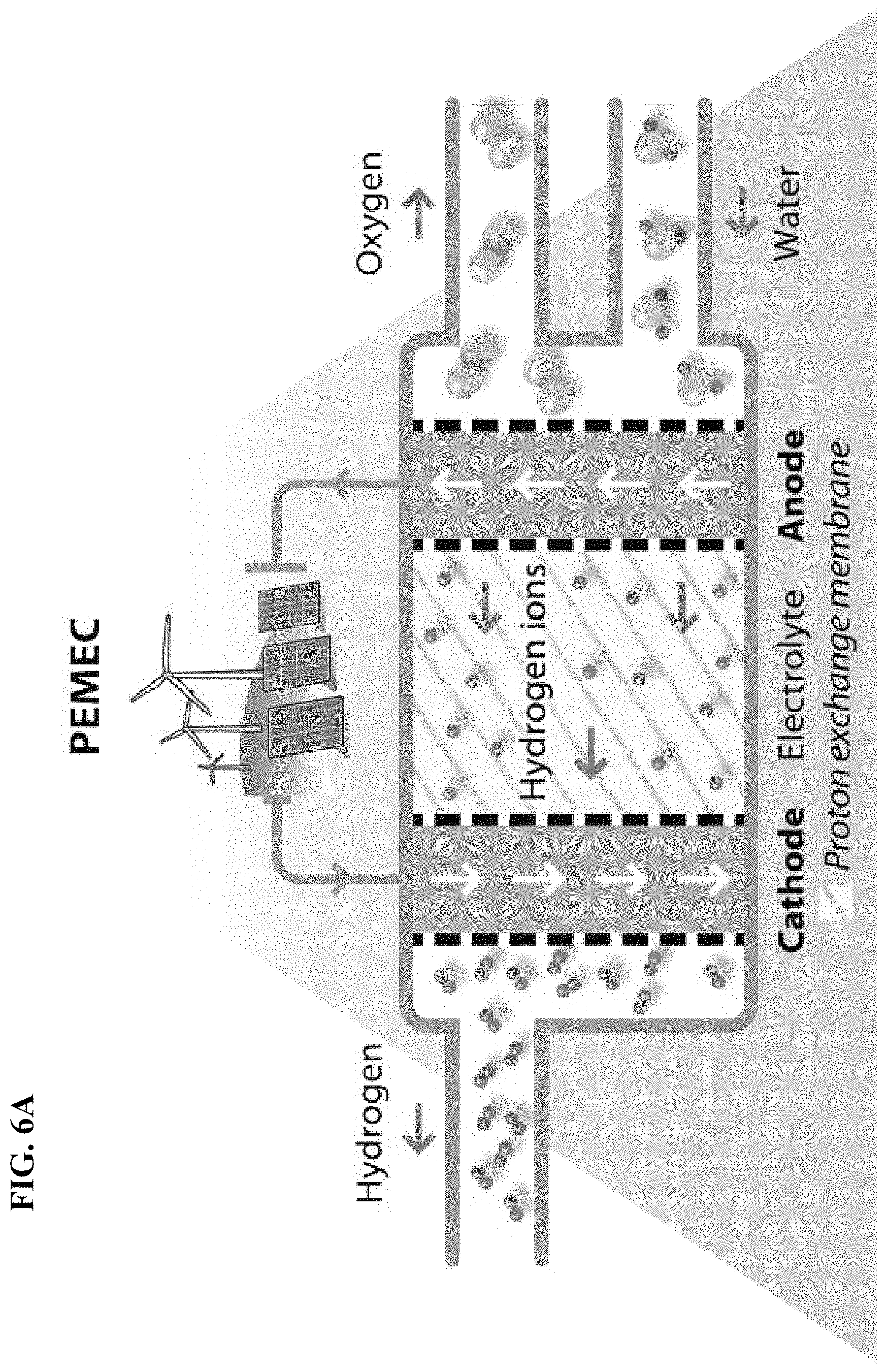
FIG. 6A depicts in accordance with various embodiments of the invention, water electrolysis and the use of a proton exchange membrane. Characteristic features of this type of technology include: (1) production of high-purity hydrogen, (2) not done at large scale size, and (3) high capital cost.
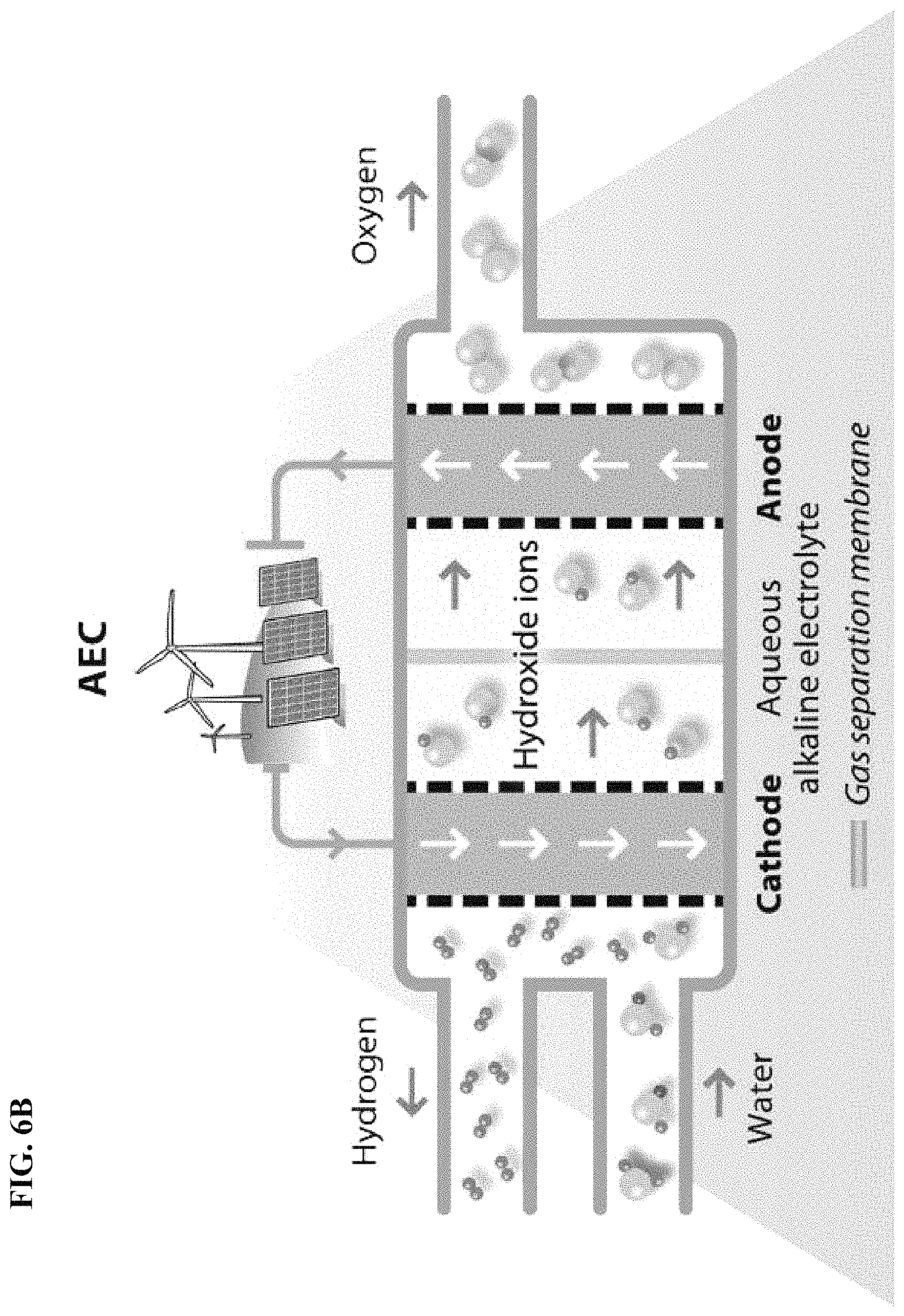
FIG. 6B depicts in accordance with various embodiments of the invention, water electrolysis and the use of a gas separation membrane. Characteristic features of this type of technology include (1) it is a mature technology, (2) relatively limited response, and (3) low-purity hydrogen is produced.
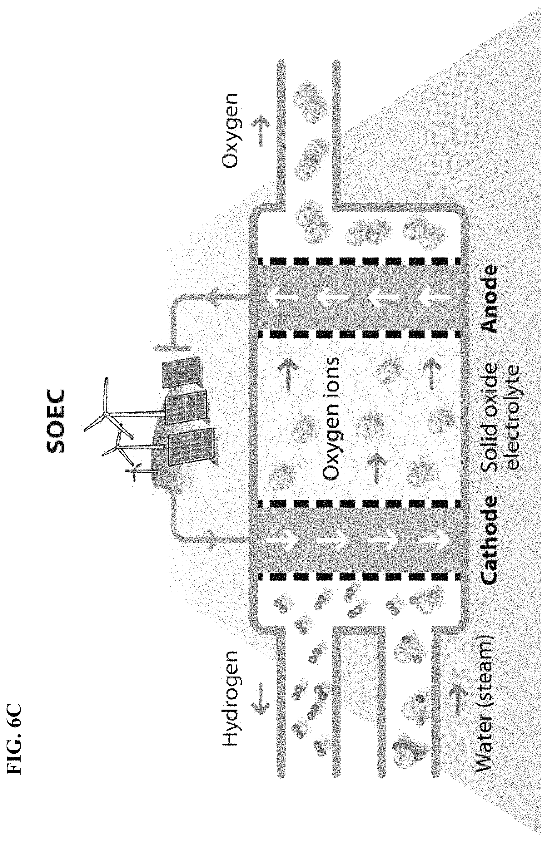
FIG. 6C depicts in accordance with various embodiments of the invention, water electrolysis and the use of a solid oxide electrolyte. Characteristic features of this type of technology include: (1) high temperature, (2) high efficiency promising, and (3) not commercialized yet.
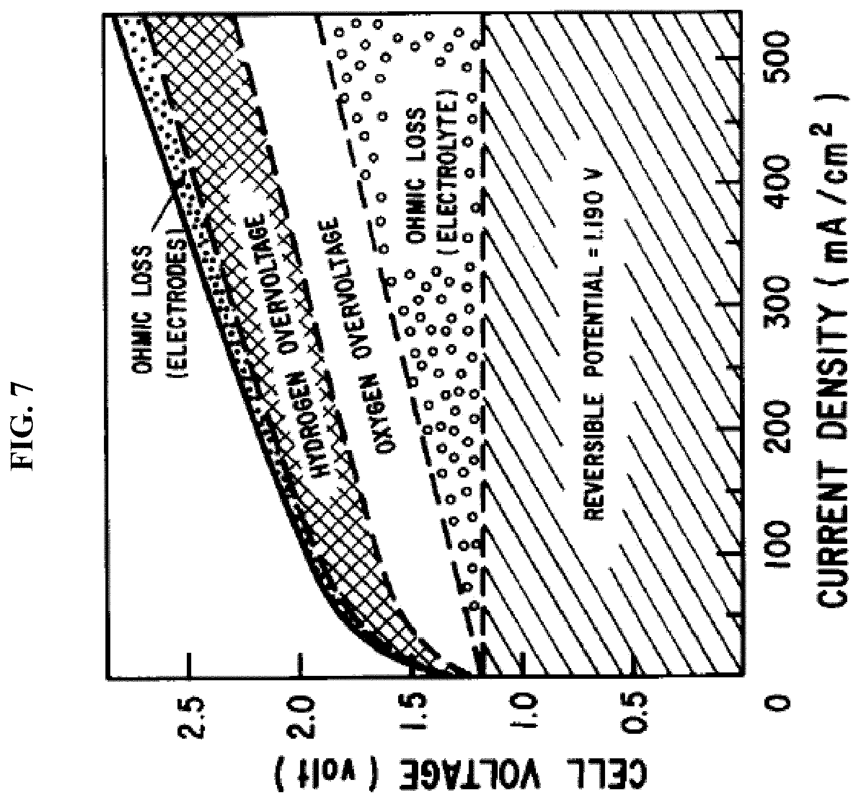
FIG. 7 depicts in accordance with various embodiments of the invention, common water electrolysis has much lower efficiency because of Ohmic loss from the electrolyte ionic current connecting the two half reactions at two electrodes, especially when current density is increasing.
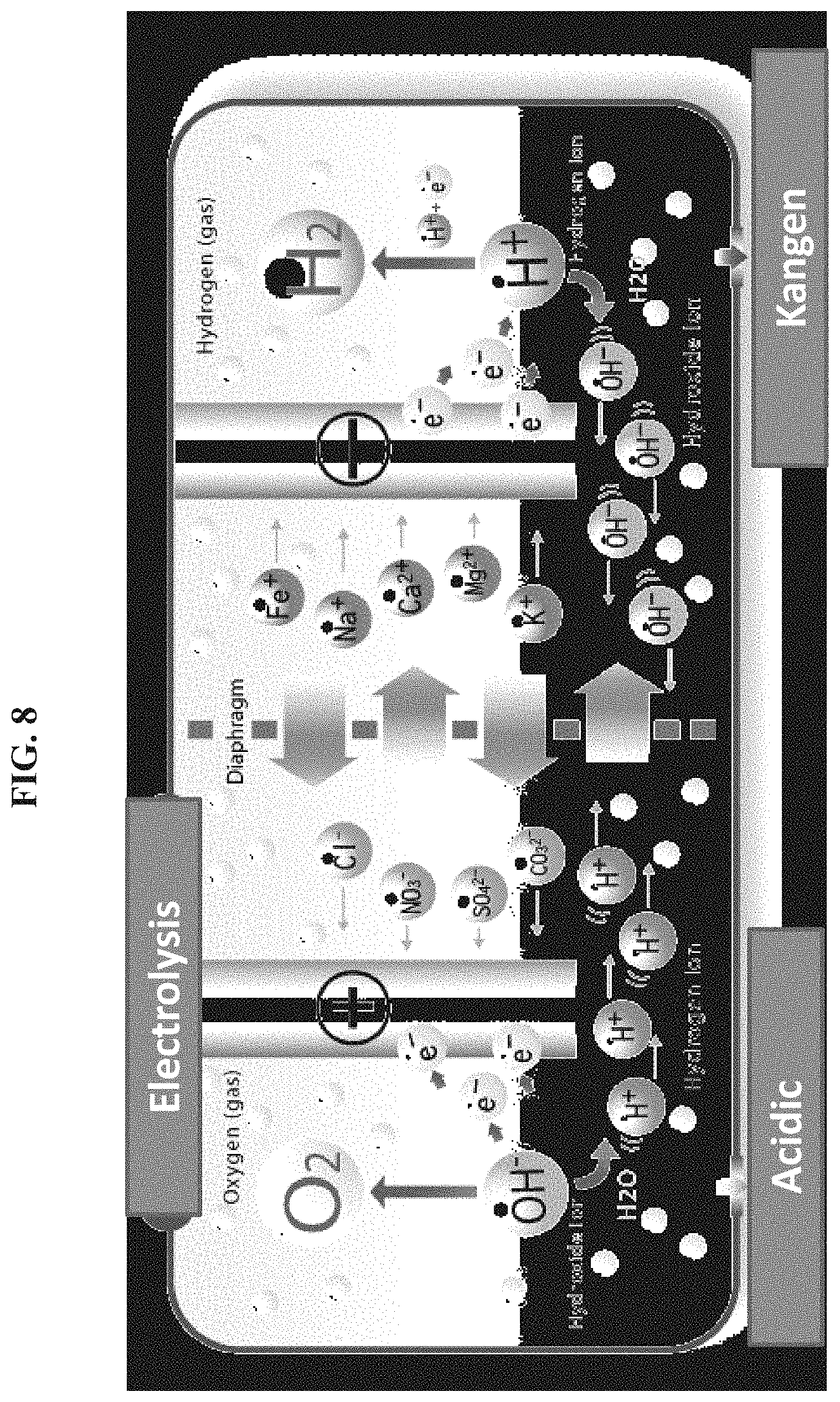
FIG. 8 depicts in accordance with various embodiments of the invention, a system for hydrogen generation. The distance between two electrodes was reduced below the Debye screening length of pure water (around 60 nm in air), to eliminate the need of electrolyte, and hence the total Ohmic loss was reduced and a much higher efficiency for hydrogen generation was achieved. Moreover, this is a portable hydrogen generation solution.
FIG. 9 depicts in accordance with various embodiments of the invention, a vertical nanoelectrode scheme, and the effect of decreasing the distance between two electrodes, in order to reduce the total Ohmic loss.
FIG. 10A-FIG. 10G depicts in accordance with various embodiments of the invention, a diagram of a fabrication process for a composition comprising nanoelectrodes.
FIG. 11A-FIG. 11C depicts in accordance with various embodiments of the invention, results of the fabrication process. The gap between two electrodes was pushed to 37 nm, much smaller than the Debye-length (around 1 .mu.m for pure water). The system used is different from a macro-system, as the mechanism for nanogapped electrodes is field-driven current rather than transportation-driven current. It was demonstrated that higher efficiency could be achieved, even at room temperature, in pure water.
FIG. 12A-FIG. 12C depict in accordance with various embodiments of the invention, I/V-curves measurement experiments by using only DI water at room temperature, no electrolytes and heating set-up were used. (FIG. 12A) I/V curves of the same pattern with different silicon nitride thickness. Obvious higher efficiency will occur with thinner silicon nitride layers. (FIG. 12B) A few bubbles generated at around 2V. (FIG. 12C) Lots of bubbles generated at around 4V.
FIG. 13A-FIG. 13C depict in accordance with various embodiments of the invention, anode (top electrode) was damaged after several I/V curves tests, shown obviously in (FIG. 13A) and (FIG. 13B). According to Pourbaix Diagram of gold (FIG. 13C), it will be oxidized under large positive potential in acidic environment. Reliability can be improved by replacing the metal with indium tin oxide (ITO) or coating one ultrathin layer of dielectric for anode protection.
FIG. 14A-FIG. 14F depicts in accordance with various embodiments of the invention, nanogapped-electrodes systems with different gap distances between two electrodes.
FIG. 15A-FIG. 15B depicts in accordance with various embodiments of the invention, a graph of I/V measurement for different gaps. A double layer forming around 1V. Independent on gap distance. Or Au oxidation around 1V.
FIG. 16 depicts in accordance with various embodiments of the invention, a graph of current (A) vs. 1/gap distance (1/nm).
FIG. 17 depicts in accordance with various embodiments of the invention, a graph of electric field (V/m) vs. normalized gap distance.
FIG. 18 depicts in accordance with various embodiments of the invention, when there is no external potential added, water molecule, H.sup.+, and OH.sup.- are randomly distributed.
FIG. 19 depicts in accordance with various embodiments of the invention, if no electrolyte is added, the reaction rate is very slow, showing "large resistance."
FIG. 20 depicts in accordance with various embodiments of the invention, for a macro-system there is a small electric field in bulk solution, so transportation limited reaction. That is why no H.sup.+ accumulates near cathode.
FIG. 21 depicts in accordance with various embodiments of the invention, the nano-system has a high electric field in the entire gap.
FIG. 22 depicts in accordance with various embodiments of the invention, theory and model analysis using a half reaction.
FIG. 23A-FIG. 23E depicts in accordance with various embodiments of the invention, graphs showing that thinner SiN will be more likely to get short-circuited at the beginning, due to sputtered nano metal pieces at the beginning.
FIG. 24A-FIG. 24D depicts in accordance with various embodiments of the invention, graphs showing sometimes there are plateaus around 2V in the first several tests, so that there are two periods.
FIG. 25A-FIG. 25B depicts in accordance with various embodiments of the invention, graphs showing sometimes the plateaus are kept the same (quite repeatable), while sometimes the current at the plateau increased.
FIG. 26A-FIG. 26B depicts in accordance with various embodiments of the invention, most of the time Imax will decrease. This is due to Au surface oxidation.
FIG. 27A-FIG. 27B depicts in accordance with various embodiments of the invention, hydrophilicity change after first test, partially due to hydrogen/OH bond and residue Au oxidation.
FIG. 28A-FIG. 28C depicts in accordance with various embodiments of the invention, anode damage. Au electrochemically oxidized after several tests.
FIG. 29 depicts in accordance with various embodiments of the invention, metal atoms sputtered out and redeposited at high DC-bias etching, leading to short-circuit between two metal layers.
FIG. 30A-FIG. 30F depicts in accordance with various embodiments of the invention, a schematic diagram of sample fabrication processes for etching recipe test.
FIG. 31 depicts in accordance with various embodiments of the invention, a piece of sample prepared for etching recipe test, with 400 nm silicon nitride and Cr grating patterns on it.
FIG. 32 depicts in accordance with various embodiments of the invention, relationship between DC-bias and capacitively coupled RF power. The scale bar is 400 nm.
FIG. 33 depicts in accordance with various embodiments of the invention, relationship between DC-bias and ICP power. The scale bar is 400 nm.
FIG. 34 depicts in accordance with various embodiments of the invention, relationship between DC-bias and the pressure in the chamber. The scale bar is 400 nm.
FIG. 35 depicts in accordance with various embodiments of the invention, relationship between DC-bias and etching gas combinations. The scale bar is 400 nm.
FIG. 36A-FIG. 36B depict in accordance with various embodiments of the invention, (FIG. 36A) typical DC-bias matching period vs time. (FIG. 36B) SEM image of a beaklike structure. The scale bar is 500 nm.
FIG. 37 depicts in accordance with various embodiments of the invention, low DC-bias silicon nitride anisotropic etching based on an inventive recipe. The scale bar is 500 nm.
FIG. 38A-FIG. 38B depict in accordance with various embodiments of the invention, (FIG. 38A) testing sample with MIM sandwiched-like structures. (FIG. 38B) SEM image of the cross section of a testing sample. The scale bar is 500 nm.
FIG. 39 depicts in accordance with various embodiments of the invention, Table 1 showing parameters of an effective recipe for low DC-bias silicon nitride etching.
FIG. 40A-FIG. 40B depict in accordance with various embodiments of the invention, high electric field distributed in the entire gap between anode and cathode in NECs. (FIG. 40A) Schematic diagram of potential distribution in macrosystem and our sandwiched-like nanogap cells. Schematic diagram of potential distribution comparison between macrosystem and our sandwiched-like nanogap cells. (FIG. 40B) Simulation results to show the electric field distribution (1-D plot and 2-D plot) between two electrodes with gap distance of 0.1 .mu.m (0.1.lamda.d, sandwiched-like NEC), 5.0 .mu.m (5.lamda.d, sandwiched-like NEC) and 100 .mu.m (macrosystem, plate electrodes).
FIG. 41A-FIG. 41C depict in accordance with various embodiments of the invention, schematic diagram of water splitting reactions in 3 different systems. (FIG. 41A) Pure water electrolysis in macrosystem is self-limited due to the lack of rapid ion transport inside bulk solution. (FIG. 41B) In sodium hydroxide solution, water splitting reaction can keep occurring but is limited by mass transport (mainly diffusion). (FIG. 41C) In nanogap cell, high electric field in the entire gap can couple the two-half reactions together and enhance water ionization and mass transport (mainly migration), leading to efficient pure water splitting limited by electron-transfer, and completely opposite pH-value distribution compared to macrosystem. In nanogap cell, high electric field in the entire gap can enhance water ionization and mass transport (mainly migration), leading to efficient pure water splitting limited by electron-transfer, and completely opposite pH-value distribution compared to that in macrosystem.
FIG. 42A-FIG. 42D depicts in accordance with various embodiments of the invention, fabrication procedures and results of our metal-dielectric-metal sandwiched-like NECs. This fabrication method can be simply applied on large area with high yield. Dimensions: the gap distance between the two electrodes, or thickness of silicon nitride, varied from 37 nm to 1.4 .mu.m; thermal silicon dioxide, 100 nm thick; Pt, 100 nm thick; Ti, 2 nm thick; gold, 40 nm thick; Cr, 10 nm thick; the contact pads were 3.5 mm by 3.5 mm; the grating regions were 1 cm by 1 mm, with different grating pitches from 10 .mu.m to 80 .mu.m.
FIG. 43A-FIG. 43D depict in accordance with various embodiments of the invention, I-V curve measurements based on our NECs with pure DI water. The experiment conditions were 22.degree. C., 1 atm, humidity: 45%, scanning step: 50 mV, hold time: 1.5 s, delay time: 1.5 s to guarantee steady state. The devices were with 40 .mu.m grating pitch and different gap distances. (FIG. 43A) Linear I-V curves showed larger current generated from smaller gap distances. (FIG. 43B) A voltage plateau around 0.9 V shown on the log I vs. V curves. (FIG. 43C) The plot of electrolysis current vs. gap distance.sup.-1 at different voltages demonstrated that the pure water splitting was limited by electron-transfer due to the high electric field in the entire gap to enhance mass transport. (FIG. 43D) Bubble generation around 2 V. Sometimes bubble generation were very few, which may result from nanobubbles dissolved into water.
FIG. 44A-FIG. 44B depict in accordance with various embodiments of the invention, comparison between pure water splitting and water splitting in 1 mol/L sodium hydroxide solution, both based on our NECs. The experiment conditions were the same in FIG. 43. The devices were with 72 nm gap distance and different grating pitches. (FIG. 44A) The relationship between electrolysis current at 1.8 V and the number of edges. The number was calculated from the grating pitches since the grating region was fixed with width of 1 mm (each grating line had two edges). (FIG. 44B) Schematic diagram of the mechanisms of the different reaction locations for pure water splitting and water splitting in sodium hydroxide solution. In FIG. 44A, the slope (increased current per edge) from the pure water curve was almost 4 times of the slope from the sodium hydroxide solution curve, indicating much larger contribution to electrolysis current from field-driven effect than from diffusion effect. The extrapolated intercept value 0.32 mA of sodium hydroxide solution indicated the nature of entire surface involved into the reaction. For pure water, the background current 0.031 mA was much smaller, probably resulting from capacitive current or ionic impurities.
FIG. 45 depicts in accordance with various embodiments of the invention, geometry and boundary conditions setting in finite element calculations.
FIG. 46 depicts in accordance with various embodiments of the invention, the equivalent effect that water molecules dissociated in the middle of the gap.
FIG. 47 depicts in accordance with various embodiments of the invention, RC-circuit model of half-reaction of water splitting in nanogap cells.
FIG. 48 depicts in accordance with various embodiments of the invention, the recipe parameters and the etching profile of our low DC-bias silicon nitride etching.
FIG. 49A-FIG. 49B depicts in accordance with various embodiments of the invention, anode damage in pure water when voltage above 5 V. The device shown here is with 72 nm gap and 40 .mu.m pitch.
FIG. 50A-FIG. 50B depict in accordance with various embodiments of the invention, bubble effects on plateaus (or peaks) around 2 V in I-V curves based on devices with 72 nm gap and 10 .mu.m pitch, (FIG. 50A) in pure water, (FIG. 50B) in sodium hydroxide solution.
FIG. 51A-FIG. 51B depict in accordance with various embodiments of the invention, evidence of the entire surface involved into the reactions in sodium hydroxide solutions. (FIG. 51A) Large droplet provided large current. (FIG. 51B) Bubbles formed at non-grating region. The devices were with 72 nm gap distance.
FIG. 52A-FIG. 52B depict in accordance with various embodiments of the invention, plateaus in log I vs. V curves from (FIG. 52A) pure water tests and (FIG. 52B) sodium hydroxide solution tests. The devices were with 72 nm gap distance.
FIG. 53A-FIG. 53B depict in accordance with various embodiments of the invention, high electric field distributed in the entire gap between anode and cathode in NECs. FIG. 53A schematic diagram of potential distribution in macrosystem and our sandwiched-like nanogap cells. FIG. 53B simulation results to show the electric field distribution (1-D plot and 2-D plot) between two electrodes with gap distance of 37 nm (minimum experimentally achieved value), 0.1 .mu.m (deep-sub-Debye-length, sandwiched-like NEC), 5.0 .mu.m (comparable to Debye-length, sandwiched-like NEC) and 100 .mu.m (macrosystem, plate electrodes).
FIG. 54A-FIG. 54B depict in accordance with various embodiments of the invention, comparison between pure water splitting and water splitting in 1 mol/L sodium hydroxide solution, both based on our NECs. The experiment conditions were the same as in FIG. 43. The devices were with 72 nm gap distance and different grating pitches. FIG. 54A the relationship between electrolysis current at 1.8 V and the number of edges. The number was calculated from the grating pitches since the width of the grating region was fixed to 1 mm (each grating line had two edges). FIG. 54B schematic diagram of the mechanisms showing the different reaction locations in pure water splitting and water splitting in sodium hydroxide solution.
FIG. 55A-FIG. 55B depict in accordance with various embodiments of the invention, a schematic of a vertical nanogap electrode system (vertical nanoelectrode system) and horizontal nanogap electrode system (horizontal nanoelectrode system). FIG. 55A shows a vertical nanoelectrode device in which two conductive layers as anode and cathode, in which there is a dielectric layer located between the anode and the cathode. The thickness of the dielectric layer is only nanometers thick (e.g., 5 nm-5 .mu.m) and the whole structure is a sandwich-like structure. The thickness of the dielectric material layer is what establishes the distance (i.e., gap or gap distance) between the cathode and the anode, and this distance is in the nanometer scale (e.g., 5 nm-5 .mu.m). FIG. 55B shows a horizontal nanoelectrode system in which both cathode and anode are fabricated in the same plane. The whole structure is comb-like structure and the space (i.e. gap or gap distance) between each finger-pair is in nanometer scale (e.g., 10 nm-5 .mu.m).
DETAILED DESCRIPTION OF THE INVENTION
All references cited herein are incorporated by reference in their entirety as though fully set forth. Unless otherwise defined, all technical and scientific terms used herein have the same meaning as commonly understood by one of ordinary skill in the art to which this invention belongs.
One skilled in the art will recognize many methods and materials similar or equivalent to those described herein, which could be used in the practice of the present invention. Other features and advantages of the invention will become apparent from the following detailed description, taken in conjunction with the accompanying drawings, which illustrate, by way of example, various features of embodiments of the invention. Indeed, the present invention is in no way limited to the methods and materials described. For convenience, certain terms employed herein, in the specification, examples and appended claims are collected here.
Unless stated otherwise, or implicit from context, the following terms and phrases include the meanings provided below. Unless explicitly stated otherwise, or apparent from context, the terms and phrases below do not exclude the meaning that the term or phrase has acquired in the art to which it pertains. Unless otherwise defined, all technical and scientific terms used herein have the same meaning as commonly understood by one of ordinary skill in the art to which this invention belongs. It should be understood that this invention is not limited to the particular methodology, protocols, and reagents, etc., described herein and as such can vary. The definitions and terminology used herein are provided to aid in describing particular embodiments, and are not intended to limit the claimed invention, because the scope of the invention is limited only by the claims.
As used herein the term "comprising" or "comprises" is used in reference to compositions, methods, systems, articles of manufacture, and respective component(s) thereof, that are useful to an embodiment, yet open to the inclusion of unspecified elements, whether useful or not. It will be understood by those within the art that, in general, terms used herein are generally intended as "open" terms (e.g., the term "including" should be interpreted as "including but not limited to," the term "having" should be interpreted as "having at least," the term "includes" should be interpreted as "includes but is not limited to," etc.). As used herein, the term "comprising" or "comprises" means that other elements can also be present in addition to the defined elements presented. The use of "comprising" indicates inclusion rather than limitation.
Unless stated otherwise, the terms "a" and "an" and "the" and similar references used in the context of describing a particular embodiment of the application (especially in the context of claims) can be construed to cover both the singular and the plural. The recitation of ranges of values herein is merely intended to serve as a shorthand method of referring individually to each separate value falling within the range. Unless otherwise indicated herein, each individual value is incorporated into the specification as if it were individually recited herein. All methods described herein can be performed in any suitable order unless otherwise indicated herein or otherwise clearly contradicted by context. The use of any and all examples, or exemplary language (for example, "such as") provided with respect to certain embodiments herein is intended merely to better illuminate the application and does not pose a limitation on the scope of the application otherwise claimed. The abbreviation, "e.g." is derived from the Latin exempli gratia, and is used herein to indicate a non-limiting example. Thus, the abbreviation "e.g." is synonymous with the term "for example." No language in the specification should be construed as indicating any non-claimed element essential to the practice of the application.
"Optional" or "optionally" means that the subsequently described circumstance may or may not occur, so that the description includes instances where the circumstance occurs and instances where it does not.
With the foregoing background in mind, in some embodiments, the invention teaches compositions, systems, articles of manufacture, and methods for water splitting and similar reactions with higher efficiency than previously reported. By decreasing the distance between two electrodes to nanometer scale, even shorter than the electric field screening length, the external power required for water splitting is significantly decreased. The deep-sub-Debye-length nanogapped electrodes systems described in certain embodiments herein, and demonstrated in certain drawings submitted herewith, lead to a high electric field inside the entire gap for enhancement of water molecule ionization, and therefore enhancement of splitting rate, transportation rate and reaction rate. Once OH.sup.- ions are generated near the cathode area, they won't accumulate there to stop the reactions, but move to the anode area under high electric field. In this way, the reactions won't self-stop. Advantageously, the inventive compositions, systems, articles of manufacture, and methods allow for water splitting at room temperature, which cannot be achieved by previous known methods. The inventive nanogapped electrodes systems have a lower overpotential, higher localized concentration, faster transport rate, and larger ionization, which can accelerate the whole reaction of water electrolysis. Different from a macro-system, the inventive systems, especially as described in the "Examples" section and drawings, are based on field-driven current, and therefore can split water even at room temperature, as indicated above. Disclosed herein and depicted in the drawings submitted herewith are both vertical nanoelectrode and horizontal nanoelectrode structures. In some embodiments, the invention also teaches a solution for anode protection during water splitting. Importantly, the technology described in the present application can be applied to most of the water splitting methods, including electrolysis, photolysis, thermolysis, and the like.
The underlying technologies of the compositions, systems, articles of manufacture, and methods can also be applied to many electrochemical industries, including hydrogen production, chlorine production, and sodium hydroxide production, just to name a few.
Hydrogen is a high energy density source, and therefore embodiments of the present invention provide for high energy density storage. The inventive nanogapped electrodes systems can combine with those renewable energy generation methods (e.g., wind electricity generation), to store hydrogen. Then, a fuel cell system can be applied to the generated hydrogen for power generation. Advantageously, by integrating with energy collection technology, embodiments of the invention also allow for a portable device for hydrogen generation.
In various embodiments, nanoelectrodes of the present invention are fabricated by nanofabrication technology, including but limited to the type described and depicted in the drawings submitted herewith and in the "Examples" section.
Two general types of nanoelectrode structures are included in the various embodiments described herein (FIG. 55A and FIG. 55B). The first general type is vertical nanoelectrodes, which include two conductive layers as anode and cathode, in which there is a dielectric layer (FIG. 55A). The thickness of the dielectric layer is only nanometers thick (e.g., 5 nm-5 .mu.m) and the whole structure is a sandwich-like structure. The thickness of the dielectric material layer is what establishes the distance (i.e., gap or gap distance) between the cathode and the anode, and this distance is in the nanometer scale (e.g., 5 nm-5 .mu.m). During the fabrication process, in order to avoid short-circuit between two conductive layers low DC-bias dry etching technology is used, as described in greater detail in the "Examples" section. The second general type of nanoelectrode structure is horizontal nanoelectrodes. In this type, both cathode and anode are fabricated in the same plane. The whole structure is comb-like structure and the space (i.e. gap or gap distance) between each finger-pair is in nanometer scale (e.g., 10 nm-5 .mu.m) (FIG. 55B). Experimentation revealed that even the most inert metal gold could not survive as anodes due to electrochemical reactions during water splitting. This effect significantly decreases the lifetime of nanoelectrode devices. As a solution to this problem, the inventors have discovered that indium-tin-oxide (ITO) can be used as anode material because it is at the highest oxidation state and could be oxidized further. Another solution to avoid anode attack is to deposit one ultra-thin dielectric layer (e.g. TiO.sub.2) on anodes as a protection layer. Besides ITO replacement and TiO.sub.2 layer protection, new methods can be used to avoid anode damage by new design of the electro layout to avoid tip field effects. The energy band of the anode and the dielectric protection layer can be engineered carefully to obtain best match between each other, in order to give higher efficiency. The voltage required based on these nanoelectrode devices is only around 1.5 V, which most portable energy collectors could achieve. Meanwhile, these devices don't require huge setup used in industrial applications, which provides a solution for portable hydrogen generation technology.
In various embodiments, the invention also teaches an effective approach for silicon nitride plasma dry etching, with low DC-bias (self-bias) and vertical sidewalls. Four main factors were considered: capacitively coupled radio frequency power, inductively coupled plasma power, pressure in the etching chamber, and the combination of etching gases. By meticulously controlling these factors, low DC-bias silicon nitride anisotropic etching without argon bombardment was successfully achieved, with DC-bias of only 34 V and etching rate of 40 nm/min (See "Examples" section). The inventive etching protocols described in the "Examples" section can avoid short-circuits effectively when patterning sub-50 nm thick silicon nitride layer as a dielectric layer between two metal layers, such as required for certain embodiments of nanoelectrodes-based systems described herein.
In various embodiments, the invention provides a system that comprises an anode and a cathode. In various embodiments, the invention provides a system that comprises an anode and a cathode, wherein the anode and the cathode are separated by a distance of 10 nm-5 .mu.m. In some embodiments, the invention teaches a system that includes an anode and a cathode, wherein said anode and cathode are separated by a distance of 10 nm-5 .mu.m. In some embodiments, the invention teaches a system that includes an anode and a cathode, wherein said anode and cathode are separated by a distance of 10 nm-20 nm, 10 nm-30 nm, 10 nm-40 nm, 10 nm-50 nm, 10 nm-60 nm, 10 nm-70 nm, 10 nm-80 nm, 10 nm-90 nm, 10 nm-0.1 .mu.m, 10 nm-0.2 .mu.m, 10 nm-0.3 .mu.m, 10 nm-0.4 .mu.m, 10 nm-0.5 .mu.m, 10 nm-0.6 .mu.m, 10 nm-0.7 .mu.m, 10 nm-0.8 .mu.m, 10 nm-0.9 .mu.m, 10 nm-1 .mu.m, 10 nm-2 .mu.m, 10 nm-3 .mu.m, 10 nm-4 .mu.m, 10 nm-5 .mu.m, 20 nm-30 nm, 20 nm-40 nm, 20 nm-50 nm, 20 nm-60 nm, 20 nm-70 nm, 20 nm-80 nm, 20 nm-90 nm, 20 nm-0.1 .mu.m, 20 nm-0.2 .mu.m, 20 nm-0.3 .mu.m, 20 nm-0.4 .mu.m, 20 nm-0.5 .mu.m, 20 nm-0.6 .mu.m, 20 nm-0.7 .mu.m, 20 nm-0.8 .mu.m, 20 nm-0.9 .mu.m, 20 nm-1 .mu.m, 20 nm-2 .mu.m, 20 nm-3 .mu.m, 20 nm-4 .mu.m, 20 nm-5 .mu.m, 30 nm-40 nm, 30 nm-50 nm, 30 nm-60 nm, 30 nm-70 nm, 30 nm-80 nm, 30 nm-90 nm, 30 nm-0.1 .mu.m, 30 nm-0.2 .mu.m, 30 nm-0.3 .mu.m, 30 nm-0.4 .mu.m, 30 nm-0.5 .mu.m, 30 nm-0.6 .mu.m, 30 nm-0.7 .mu.m, 30 nm-0.8 .mu.m, 30 nm-0.9 .mu.m, 30 nm-1 .mu.m, 30 nm-2 .mu.m, 30 nm-3 .mu.m, 30 nm-4 .mu.m, or 30 nm-5 .mu.m. In some embodiments, the invention teaches a system that includes an anode and a cathode, wherein said anode and cathode are separated by a distance of 37 nm. In some embodiments, the invention teaches a system that includes an anode and a cathode, wherein said anode and cathode are separated by a distance of 10 nm-20 nm, 10 nm-30 nm, 10 nm-40 nm, 10 nm-50 nm, 10 nm-60 nm, 10 nm-70 nm, 10 nm-80 nm, 10 nm-90 nm, 10 nm-100 nm, 10 nm-150 nm, 10 nm-200 nm, 10 nm-250 nm, 10 nm-300 nm, 10 nm-350 nm, 10 nm-400 nm, 10 nm-450 nm, 10 nm-500 nm, 10 nm-550 nm, 10 nm-600 nm, 10 nm-650 nm, 10 nm-700 nm, 10 nm-750 nm, 10 nm-800 nm, 10 nm-850 nm, 10 nm-900 nm, 10 nm-950 nm, 10 nm-1000 nm, 10 nm-1100 nm, 10 nm-1200 nm, 10 nm-1300 nm, 10 nm-1400 nm, 10 nm-1500 nm, 10 nm-1600 nm, 10 nm-1700 nm, 10 nm-1800 nm, 10 nm-1900 nm, or 10 nm-2000 nm. In some embodiments, the invention teaches a system that includes and anode and a cathode, wherein said anode and cathode are separated by a distance of 10 nm-2 .mu.m. In some embodiments, the invention teaches a system that includes and anode and a cathode, wherein said anode and cathode are separated by a distance of 10 nm-1 .mu.m. In some embodiments, the invention teaches a system that includes and anode and a cathode, wherein said anode and cathode are separated by a distance of 10 nm-500 nm.
In some embodiments, the system further comprises a dielectric material positioned or situated between the anode and the cathode. In some embodiments, the system further includes a dielectric material situated between the anode and cathode. In some embodiments, the dielectric material is 5-100 nm, 100-200 nm, 200-500 nm, 500 nm-5 .mu.m (or more) thick. In some embodiments, the dielectric material thickness is 5 nm-10 nm, 5 nm-20 nm, 5 nm-30 nm, 5 nm-40 nm, 5 nm-50 nm, 5 nm-60 nm, 5 nm-70 nm, 5 nm-80 nm, 5 nm-90 nm, 5 nm-100 nm, 5 nm-200 nm, 5 nm-300 nm, 5 nm-400 nm, 5 nm-500 nm, 5 nm-1 .mu.m, 5 nm-2 .mu.m, 5 nm-3 .mu.m, 5 nm-4 .mu.m, 5 nm-5 .mu.m, 10 nm-20 nm, 10 nm-30 nm, 10 nm-40 nm, 10 nm-50 nm, 10 nm-60 nm, 10 nm-70 nm, 10 nm-80 nm, 10 nm-90 nm, 10 nm-100 nm, 10 nm-200 nm, 10 nm-300 nm, 10 nm-400 nm, 10 nm-500 nm, 10 nm-1 .mu.m, 10 nm-2 .mu.m, 10 nm-3 .mu.m, 10 nm-4 .mu.m, 10 nm-5 .mu.m, 20 nm-30 nm, 20 nm-40 nm, 20 nm-50 nm, 20 nm-60 nm, 20 nm-70 nm, 20 nm-80 nm, 20 nm-90 nm, 20 nm-100 nm, 20 nm-200 nm, 20 nm-300 nm, 20 nm-400 nm, 20 nm-500 nm, 20 nm-1 .mu.m, 20 nm-2 .mu.m, 20 nm-3 .mu.m, 20 nm-4 .mu.m, 20 nm-5 .mu.m, 30 nm-40 nm, 30 nm-50 nm, 30 nm-60 nm, 30 nm-70 nm, 30 nm-80 nm, 30 nm-90 nm, 30 nm-100 nm, 30 nm-200 nm, 30 nm-300 nm, 30 nm-400 nm, 30 nm-500 nm, 30 nm-1 .mu.m, 30 nm-2 .mu.m, 30 nm-3 .mu.m, 30 nm-4 .mu.m or 30 nm-5 .mu.m. In some embodiments, the system further includes a dielectric material situated between the anode and cathode, wherein the dielectric material thickness is 10 nm-20 nm, 10 nm-30 nm, 10 nm-40 nm, 10 nm-50 nm, 10 nm-60 nm, 10 nm-70 nm, 10 nm-80 nm, 10 nm-90 nm, 10 nm-100 nm, 10 nm-150 nm, 10 nm-200 nm, 10 nm-250 nm, 10 nm-300 nm, 10 nm-350 nm, 10 nm-400 nm, 10 nm-450 nm, 10 nm-500 nm, 10 nm-550 nm, 10 nm-600 nm, 10 nm-650 nm, 10 nm-700 nm, 10 nm-750 nm, 10 nm-800 nm, 10 nm-850 nm, 10 nm-900 nm, 10 nm-950 nm, 10 nm-1000 nm, 10 nm-1100 nm, 10 nm-1200 nm, 10 nm-1300 nm, 10 nm-1400 nm, 10 nm-1500 nm, 10 nm-1600 nm, 10 nm-1700 nm, 10 nm-1800 nm, 10 nm-1900 nm, or 10 nm-2000 nm. In some embodiments, the system further includes a dielectric material situated between the anode and cathode, wherein the dielectric material thickness is 10 nm-2 .mu.m. In some embodiments, the system further includes a dielectric material situated between the anode and cathode, wherein the dielectric material thickness is 10 nm-1 .mu.m. In some embodiments, the system further includes a dielectric material situated between the anode and cathode, wherein the dielectric material thickness is 10 nm-500 nm.
In certain embodiments, a portion of the anode is coated with a dielectric material. In some embodiments, the dielectric material of the system includes silicon nitride. In some embodiments, the cathode of the system includes Ti and/or Pt. In certain embodiments, the anode of the system includes indium-tin-oxide (ITO). In some embodiments, the anode of the system includes Ti and/or Au, or Ni. In some embodiments, the system further includes a layer of silicon substrate in contact with the cathode. In some embodiments, the system, with or without a layer of dielectric material between the anode and cathode, further includes water.
In some embodiments, the invention teaches an article of manufacture that comprises an anode and a cathode. In some embodiments, the invention teaches an article of manufacture that comprises an anode and a cathode, wherein said anode and cathode are separated by a distance of 10 nm-5 .mu.m. In some embodiments, the invention teaches an article of manufacture that includes an anode and a cathode, wherein said anode and cathode are separated by a distance of 10 nm-5 .mu.m. In some embodiments, the invention teaches an article of manufacture that includes an anode and a cathode, wherein said anode and cathode are separated by a distance of 10 nm-20 nm, 10 nm-30 nm, 10 nm-40 nm, 10 nm-50 nm, 10 nm-60 nm, 10 nm-70 nm, 10 nm-80 nm, 10 nm-90 nm, 10 nm-0.1 .mu.m, 10 nm-0.2 .mu.m, 10 nm-0.3 .mu.m, 10 nm-0.4 .mu.m, 10 nm-0.5 .mu.m, 10 nm-0.6 .mu.m, 10 nm-0.7 .mu.m, 10 nm-0.8 .mu.m, 10 nm-0.9 .mu.m, 10 nm-1 .mu.m, 10 nm-2 .mu.m, 10 nm-3 .mu.m, 10 nm-4 .mu.m, 10 nm-5 .mu.m, 20 nm-30 nm, 20 nm-40 .mu.m, 20 nm-50 nm, 20 nm-60 nm, 20 nm-70 nm, 20 nm-80 nm, 20 nm-90 nm, 20 nm-0.1 .mu.m, 20 nm-0.2 .mu.m, 20 nm-0.3 .mu.m, 20 nm-0.4 .mu.m, 20 nm-0.5 .mu.m, 20 nm-0.6 .mu.m, 20 nm-0.7 .mu.m, 20 nm-0.8 .mu.m, 20 nm-0.9 .mu.m, 20 nm-1 .mu.m, 20 nm-2 .mu.m, 20 nm-3 .mu.m, 20 nm-4 .mu.m, 20 nm-5 .mu.m, 30 nm-40 nm, 30 nm-50 nm, 30 nm-60 nm, 30 nm-70 nm, 30 nm-80 nm, 30 nm-90 nm, 30 nm-0.1 .mu.m, 30 nm-0.2 .mu.m, 30 nm-0.3 .mu.m, 30 nm-0.4 .mu.m, 30 nm-0.5 .mu.m, 30 nm-0.6 .mu.m, 30 nm-0.7 .mu.m, 30 nm-0.8 .mu.m, 30 nm-0.9 .mu.m, 30 nm-1 .mu.m, 30 nm-2 .mu.m, 30 nm-3 .mu.m, 30 nm-4 .mu.m, or 30 nm-5 .mu.m. In some embodiments, the invention teaches an article of manufacture that includes an anode and a cathode, wherein said anode and cathode are separated by a distance of 37 nm. In some embodiments, the invention teaches an article of manufacture that includes an anode and a cathode, wherein said anode and cathode are separated by a distance of 10 nm-20 nm, 10 nm-30 nm, 10 nm-40 nm, 10 nm-50 nm, 10 nm-60 nm, 10 nm-70 nm, 10 nm-80 nm, 10 nm-90 nm, 10 nm-100 nm, 10 nm-150 nm, 10 nm-200 nm, 10 nm-250 nm, 10 nm-300 nm, 10 nm-350 nm, 10 nm-400 nm, 10 nm-450 nm, 10 nm-500 nm, 10 nm-550 nm, 10 nm-600 nm, 10 nm-650 nm, 10 nm-700 nm, 10 nm-750 nm, 10 nm-800 nm, 10 nm-850 nm, 10 nm-900 nm, 10 nm-950 nm, 10 nm-1000 nm, 10 nm-1100 nm, 10 nm-1200 nm, 10 nm-1300 nm, 10 nm-1400 nm, 10 nm-1500 nm, 10 nm-1600 nm, 10 nm-1700 nm, 10 nm-1800 nm, 10 nm-1900 nm, or 10 nm-2000 nm. In some embodiments, the invention teaches an article of manufacture that includes an anode and a cathode, wherein said anode and cathode are separated by a distance of 10 nm-2 .mu.m. In some embodiments, the invention teaches an article of manufacture that includes an anode and a cathode, wherein said anode and cathode are separated by a distance of 10 nm-1 .mu.m. In some embodiments, the invention teaches an article of manufacture that includes an anode and a cathode, wherein said anode and cathode are separated by a distance of 10 nm-500 nm.
In some embodiments, the article of manufacture further comprises a dielectric material situated between the anode and cathode. In some embodiments, the article of manufacture further includes a dielectric material situated between the anode and cathode. In some embodiments, the dielectric material is 5-100 nm, 100-200 nm, 200-500 nm, 500 nm-5 .mu.m (or more) thick. In some embodiments, the dielectric material is 5 nm-10 nm, 5 nm-20 nm, 5 nm-30 nm, 5 nm-40 nm, 5 nm-50 nm, 5 nm-60 nm, 5 nm-70 nm, 5 nm-80 nm, 5 nm-90 nm, 5 nm-100 nm, 5 nm-200 nm, 5 nm-300 nm, 5 nm-400 nm, 5 nm-500 nm, 5 nm-1 .mu.m, 5 nm-2 .mu.m, 5 nm-3 .mu.m, 5 nm-4 .mu.m, 5 nm-5 .mu.m, 10 nm-20 nm, 10 nm-30 nm, 10 nm-40 nm, 10 nm-50 nm, 10 nm-60 nm, 10 nm-70 nm, 10 nm-80 nm, 10 nm-90 nm, 10 nm-100 nm, 10 nm-200 nm, 10 nm-300 nm, 10 nm-400 nm, 10 nm-500 nm, 10 nm-1 .mu.m, 10 nm-2 .mu.m, 10 nm-3 .mu.m, 10 nm-4 .mu.m, 10 nm-5 .mu.m, 20 nm-30 nm, 20 nm-40 nm, 20 nm-50 nm, 20 nm-60 nm, 20 nm-70 nm, 20 nm-80 nm, 20 nm-90 nm, 20 nm-100 nm, 20 nm-200 nm, 20 nm-300 nm, 20 nm-400 nm, 20 nm-500 nm, 20 nm-1 .mu.m, 20 nm-2 .mu.m, 20 nm-3 .mu.m, 20 nm-4 .mu.m, 20 nm-5 .mu.m, 30 nm-40 nm, 30 nm-50 nm, 30 nm-60 nm, 30 nm-70 nm, 30 nm-80 nm, 30 nm-90 nm, 30 nm-100 nm, 30 nm-200 nm, 30 nm-300 nm, 30 nm-400 nm, 30 nm-500 nm, 30 nm-1 .mu.m, 30 nm-2 .mu.m, 30 nm-3 .mu.m, 30 nm-4 .mu.m, or 30 nm-5 .mu.m. In some embodiments, the article of manufacture further includes a dielectric material situated between the anode and cathode, wherein the dielectric material thickness is 10 nm-20 nm, 10 nm-30 nm, 10 nm-40 nm, 10 nm-50 nm, 10 nm-60 nm, 10 nm-70 nm, 10 nm-80 nm, 10 nm-90 nm, 10 nm-100 nm, 10 nm-150 nm, 10 nm-200 nm, 10 nm-250 nm, 10 nm-300 nm, 10 nm-350 nm, 10 nm-400 nm, 10 nm-450 nm, 10 nm-500 nm, 10 nm-550 nm, 10 nm-600 nm, 10 nm-650 nm, 10 nm-700 nm, 10 nm-750 nm, 10 nm-800 nm, 10 nm-850 nm, 10 nm-900 nm, 10 nm-950 nm, 10 nm-1000 nm, 10 nm-1100 nm, 10 nm-1200 nm, 10 nm-1300 nm, 10 nm-1400 nm, 10 nm-1500 nm, 10 nm-1600 nm, 10 nm-1700 nm, 10 nm-1800 nm, 10 nm-1900 nm, or 10 nm-2000 nm. In some embodiments, the article of manufacture further includes a dielectric material situated between the anode and cathode, wherein the dielectric material thickness is 10 nm-2 .mu.m. In some embodiments, the article of manufacture further includes a dielectric material situated between the anode and cathode, wherein the dielectric material thickness is 10 nm-1 .mu.m. In some embodiments, the article of manufacture further includes a dielectric material situated between the anode and cathode, wherein the dielectric material thickness is 10 nm-500 nm.
In certain embodiments, a portion of the anode is coated with a dielectric material. In some embodiments, the dielectric material of the article of manufacture includes silicon nitride. In some embodiments, the cathode of the article of manufacture includes Ti and/or Pt. In certain embodiments, the anode of the article of manufacture includes indium-tin-oxide (ITO). In some embodiments, the anode of the article of manufacture includes Ti and/or Au, or Ni. In some embodiments, the article of manufacture further includes a layer of silicon substrate in contact with the cathode. In some embodiments, the article of manufacture, with or without a layer of dielectric material between the anode and cathode, further includes water.
In various embodiments, the invention teaches a composition that comprises an anode and a cathode. In various embodiments, the invention teaches a composition that comprises an anode, a cathode, and a dielectric material, wherein the dielectric material is positioned between the anode and the cathode. In various embodiments, the invention teaches a composition that includes an anode, a cathode, and a dielectric material situated between the anode and cathode. In some embodiments, the dielectric material is 5-100 nm, 100-200 nm, 200-500 nm, 500 nm-5 .mu.m (or more) thick. In some embodiments, the dielectric material is 5 nm-10 nm, 5 nm-20 nm, 5 nm-30 nm, 5 nm-40 nm, 5 nm-50 nm, 5 nm-60 nm, 5 nm-70 nm, 5 nm-80 nm, 5 nm-90 nm, 5 nm-100 nm, 5 nm-200 nm, 5 nm-300 nm, 5 nm-400 nm, 5 nm-500 nm, 5 nm-1 .mu.m, 5 nm-2 .mu.m, 5 nm-3 .mu.m, 5 nm-4 .mu.m, 5 nm-5 .mu.m, 10 nm-20 nm, 10 nm-30 nm, 10 nm-40 nm, 10 nm-50 nm, 10 nm-60 nm, 10 nm-70 nm, 10 nm-80 nm, 10 nm-90 nm, 10 nm-100 nm, 10 nm-200 nm, 10 nm-300 nm, 10 nm-400 nm, 10 nm-500 nm, 10 nm-1 .mu.m, 10 nm-2 .mu.m, 10 nm-3 .mu.m, 10 nm-4 .mu.m, 10 nm-5 .mu.m, 20 nm-30 nm, 20 nm-40 nm, 20 nm-50 nm, 20 nm-60 nm, 20 nm-70 nm, 20 nm-80 nm, 20 nm-90 nm, 20 nm-100 nm, 20 nm-200 nm, 20 nm-300 nm, 20 nm-400 nm, 20 nm-500 nm, 20 nm-1 .mu.m, 20 nm-2 .mu.m, 20 nm-3 .mu.m, 20 nm-4 .mu.m, 20 nm-5 .mu.m, 30 nm-40 nm, 30 nm-50 nm, 30 nm-60 nm, 30 nm-70 nm, 30 nm-80 nm, 30 nm-90 nm, 30 nm-100 nm, 30 nm-200 nm, 30 nm-300 nm, 30 nm-400 nm, 30 nm-500 nm, 30 nm-1 .mu.m, 30 nm-2 .mu.m, 30 nm-3 .mu.m, 30 nm-4 .mu.m, or 30 nm-5 .mu.m. In some embodiments, the invention teaches a composition that includes an anode, a cathode, and a dielectric material situated between the anode and cathode, wherein the dielectric material thickness is 10 nm-20 nm, 10 nm-30 nm, 10 nm-40 nm, 10 nm-50 nm, 10 nm-60 nm, 10 nm-70 nm, 10 nm-80 nm, 10 nm-90 nm, 10 nm-100 nm, 10 nm-150 nm, 10 nm-200 nm, 10 nm-250 nm, 10 nm-300 nm, 10 nm-350 nm, 10 nm-400 nm, 10 nm-450 nm, 10 nm-500 nm, 10 nm-550 nm, 10 nm-600 nm, 10 nm-650 nm, 10 nm-700 nm, 10 nm-750 nm, 10 nm-800 nm, 10 nm-850 nm, 10 nm-900 nm, 10 nm-950 nm, 10 nm-1000 nm, 10 nm-1100 nm, 10 nm-1200 nm, 10 nm-1300 nm, 10 nm-1400 nm, 10 nm-1500 nm, 10 nm-1600 nm, 10 nm-1700 nm, 10 nm-1800 nm, 10 nm-1900 nm, or 10 nm-2000 nm. In some embodiments, the invention teaches a composition that includes an anode, a cathode, and a dielectric material situated between the anode and cathode, wherein the dielectric material thickness is 10 nm-2 .mu.m. In some embodiments, the invention teaches a composition that includes an anode, a cathode, and a dielectric material situated between the anode and cathode, wherein the dielectric material thickness is 10 nm-1 .mu.m. In some embodiments, the invention teaches a composition that includes an anode, a cathode, and a dielectric material situated between the anode and cathode, wherein the dielectric material thickness is 10 nm-500 nm.
In some embodiments, the dielectric material includes silicon nitride. In some embodiments, the cathode includes Ti and/or Pt. In some embodiments, the anode includes indium-tin-oxide. In certain embodiments, the anode includes Ti and/or Au, or Ni. In some embodiments, the system further includes a layer of silicon substrate in contact with said cathode. In some embodiments, said anode and cathode are separated by a distance of 10 nm-5 .mu.m. In some embodiments, said anode and cathode are separated by a distance of 10 nm-20 nm, 10 nm-30 nm, 10 nm-40 nm, 10 nm-50 nm, 10 nm-60 nm, 10 nm-70 nm, 10 nm-80 nm, 10 nm-90 nm, 10 nm-0.1 .mu.m, 10 nm-0.2 .mu.m, 10 nm-0.3 .mu.m, 10 nm-0.4 .mu.m, 10 nm-0.5 .mu.m, 10 nm-0.6 .mu.m, 10 nm-0.7 .mu.m, 10 nm-0.8 .mu.m, 10 nm-0.9 .mu.m, 10 nm-1 .mu.m, 10 nm-2 .mu.m, 10 nm-3 .mu.m, 10 nm-4 .mu.m, 10-5 .mu.m, 20 nm-30 nm, 20 nm-40 nm, 20 nm-50 nm, 20 nm-60 nm, 20 nm-70 nm, 20 nm-80 nm, 20 nm-90 nm, 20 nm-0.1 .mu.m, 20 nm-0.2 .mu.m, 20 nm-0.3 .mu.m, 20 nm-0.4 .mu.m, 20 nm-0.5 .mu.m, 20 nm-0.6 .mu.m, 20 nm-0.7 .mu.m, 20 nm-0.8 .mu.m, 20 nm-0.9 .mu.m, 20 nm-1 .mu.m, 20 nm-2 .mu.m, 20 nm-3 .mu.m, 20 nm-4 .mu.m, 20 nm-5 .mu.m, 30 nm-40 nm, 30 nm-50 nm, 30 nm-60 nm, 30 nm-70 nm, 30 nm-80 nm, 30 nm-90 nm, 30 nm-0.1 .mu.m, 30 nm-0.2 .mu.m, 30 nm-0.3 .mu.m, 30 nm-0.4 .mu.m, 30 nm-0.5 .mu.m, 30 nm-0.6 .mu.m, 30 nm-0.7 .mu.m, 30 nm-0.8 .mu.m, 30 nm-0.9 .mu.m, 30 nm-1 .mu.m, 30 nm-2 .mu.m, 30 nm-3 .mu.m, 30 nm-4 .mu.m, or 30 nm-5 .mu.m. In some embodiments, said anode and cathode are separated by a distance of 37 nm. In some embodiments, said anode and cathode are separated by a distance of 10 nm-20 nm, 10 nm-30 nm, 10 nm-40 nm, 10 nm-50 nm, 10 nm-60 nm, 10 nm-70 nm, 10 nm-80 nm, 10 nm-90 nm, 10 nm-100 nm, 10 nm-150 nm, 10 nm-200 nm, 10 nm-250 nm, 10 nm-300 nm, 10 nm-350 nm, 10 nm-400 nm, 10 nm-450 nm, 10 nm-500 nm, 10 nm-550 nm, 10 nm-600 nm, 10 nm-650 nm, 10 nm-700 nm, 10 nm-750 nm, 10 nm-800 nm, 10 nm-850 nm, 10 nm-900 nm, 10 nm-950 nm, 10 nm-1000 nm, 10 nm-1100 nm, 10 nm-1200 nm, 10 nm-1300 nm, 10 nm-1400 nm, 10 nm-1500 nm, 10 nm-1600 nm, 10 nm-1700 nm, 10 nm-1800 nm, 10 nm-1900 nm, or 10 nm-2000 nm. In some embodiments, said anode and cathode are separated by a distance of 10 nm-2 .mu.m. In some embodiments, said anode and cathode are separated by a distance of 10 nm-1 .mu.m. In some embodiments, said anode and cathode are separated by a distance of 10 nm-500 nm.
In various embodiments, the present invention provides a system comprising an anode and a cathode, wherein said anode and cathode are separated by a distance of 10 nm-5 .mu.m. In some embodiments, the system further comprises a dielectric material situated between the anode and cathode. In some embodiments, a portion of the anode is coated with a dielectric material. In some embodiments, the dielectric material comprises silicon nitride. In some embodiments, the cathode comprises Ti and/or Pt. In some embodiments, the anode comprises indium-tin-oxide (ITO). In some embodiments, the anode comprises Ti and/or Au, or Ni. In some embodiments, the system further comprises a layer of silicon substrate in contact with said cathode. In some embodiments, the system further comprises water.
In various embodiments, the present invention provides a composition comprising an anode, a cathode, and a dielectric material situated between the anode and cathode. In some embodiments, the dielectric material is 10 nm-5 .mu.m thick. In some embodiments, the dielectric material comprises silicon nitride. In some embodiments, the cathode comprises Ti and/or Pt. In some embodiments, the anode comprises Ti and/or Au, or Ni. In some embodiments, the composition further comprises a layer of silicon substrate in contact with said cathode.
In various embodiments, the present invention provides a method for generating hydrogen, comprising applying an electric current to a system of the invention so as to create an electric field between the anode and cathode.
In various embodiments, the present invention provides a method for fabricating a nanoelectrode device, comprising: depositing a cathode metal on a substrate to provide a cathode; depositing a dielectric material on said cathode; and depositing an anode metal on said dielectric material to provide an anode. In some embodiments, the nanoelectrode device is a vertical nanoelectrode.
In various embodiments, the invention teaches a method for generating hydrogen. In some embodiments, the method includes applying an electric current to the systems including water described above or demonstrated in the drawings submitted herewith, so as to create an electric field between the anode and cathode, and thereby generate hydrogen.
In various embodiments, the invention teaches a method for generating hydrogen. In some embodiments, the method includes applying an electric current to the articles of manufacture including water described above or demonstrated in the drawings submitted herewith, so as to create an electric field between the anode and cathode, and thereby generate hydrogen.
In various embodiments, the invention teaches a method for fabricating a nanoelectrode device, comprising: depositing a cathode metal on a substrate to provide a cathode; and depositing an anode metal on the substrate to provide an anode, wherein said cathode and said anode are separated by a distance of 10 nm-5 .mu.m. In some embodiments, said anode and cathode are separated by a distance of 10 nm-20 nm, 10 nm-30 nm, 10 nm-40 nm, 10 nm-50 nm, 10 nm-60 nm, 10 nm-70 nm, 10 nm-80 nm, 10 nm-90 nm, 10 nm-0.1 .mu.m, 10 nm-0.2 .mu.m, 10 nm-0.3 .mu.m, 10 nm-0.4 .mu.m, 10 nm-0.5 .mu.m, 10 nm-0.6 .mu.m, 10 nm-0.7 .mu.m, 10 nm-0.8 .mu.m, 10 nm-0.9 .mu.m, 10 nm-1 .mu.m, 10 nm-2 .mu.m, 10 nm-3 .mu.m, 10 nm-4 .mu.m, 10-5 .mu.m, 20 nm-30 nm, 20 nm-40 nm, 20 nm-50 nm, 20 nm-60 nm, 20 nm-70 nm, 20 nm-80 nm, 20 nm-90 nm, 20 nm-0.1 .mu.m, 20 nm-0.2 .mu.m, 20 nm-0.3 .mu.m, 20 nm-0.4 .mu.m, 20 nm-0.5 .mu.m, 20 nm-0.6 .mu.m, 20 nm-0.7 .mu.m, 20 nm-0.8 .mu.m, 20 nm-0.9 .mu.m, 20 nm-1 .mu.m, 20 nm-2 .mu.m, 20 nm-3 .mu.m, 20 nm-4 .mu.m, 20 nm-5 .mu.m, 30 nm-40 nm, 30 nm-50 nm, 30 nm-60 nm, 30 nm-70 nm, 30 nm-80 nm, 30 nm-90 nm, 30 nm-0.1 .mu.m, 30 nm-0.2 .mu.m, 30 nm-0.3 .mu.m, 30 nm-0.4 .mu.m, 30 nm-0.5 .mu.m, 30 nm-0.6 .mu.m, 30 nm-0.7 .mu.m, 30 nm-0.8 .mu.m, 30 nm-0.9 .mu.m, 30 nm-1 .mu.m, 30 nm-2 .mu.m, 30 nm-3 .mu.m, 30 nm-4 .mu.m, or 30 nm-5 .mu.m. In some embodiments, said anode and cathode are separated by a distance of 37 nm. In some embodiments, said anode and cathode are separated by a distance of 10 nm-20 nm, 10 nm-30 nm, 10 nm-40 nm, 10 nm-50 nm, 10 nm-60 nm, 10 nm-70 nm, 10 nm-80 nm, 10 nm-90 nm, 10 nm-100 nm, 10 nm-150 nm, 10 nm-200 nm, 10 nm-250 nm, 10 nm-300 nm, 10 nm-350 nm, 10 nm-400 nm, 10 nm-450 nm, 10 nm-500 nm, 10 nm-550 nm, 10 nm-600 nm, 10 nm-650 nm, 10 nm-700 nm, 10 nm-750 nm, 10 nm-800 nm, 10 nm-850 nm, 10 nm-900 nm, 10 nm-950 nm, 10 nm-1000 nm, 10 nm-1100 nm, 10 nm-1200 nm, 10 nm-1300 nm, 10 nm-1400 nm, 10 nm-1500 nm, 10 nm-1600 nm, 10 nm-1700 nm, 10 nm-1800 nm, 10 nm-1900 nm, or 10 nm-2000 nm. In some embodiments, said anode and cathode are separated by a distance of 10 nm-2 .mu.m. In some embodiments, said anode and cathode are separated by a distance of 10 nm-1 .mu.m. In some embodiments, said anode and cathode are separated by a distance of 10 nm-500 nm. In various embodiments, the invention teaches a method for fabricating a nanoelectrode device, comprising: (a) assembling a cathode and an anode, wherein the cathode is prepared by depositing a cathode metal on a substrate, and wherein the anode is prepared by depositing an anode metal on the substrate to provide an anode, wherein said cathode and said anode are separated by a distance of 10 nm-5 .mu.m. In some embodiments, the nanoelectrode device is a horizontal nanoelectrode. In some embodiments, the cathode has a comb-like structure. In some embodiments, the anode has a comb-like structure. In some embodiments, the horizontal nanoelectrode may have the structure as shown in FIG. 55B.
In various embodiments, the invention teaches a method for fabricating a nanoelectrode device, comprising: (a) assembling a cathode and an anode, having a dielectric material between said cathode and said anode, wherein the cathode is prepared by depositing a cathode metal on a substrate, and depositing a layer of a dielectric material on said cathode, and wherein the anode is prepared by depositing an anode metal on said dielectric material. In various embodiments, the invention teaches a method for fabricating a nanoelectrode device, comprising: depositing a cathode metal on a substrate to provide a cathode; depositing a layer of a dielectric material on said cathode; and depositing an anode metal onto the dielectric material to provide an anode. In various embodiments, the invention teaches a method for fabricating a nanoelectrode device, comprising: depositing a cathode metal on a substrate to provide a cathode; depositing a dielectric material on said cathode; and depositing an anode metal on said dielectric material to provide an anode. In some embodiments, the method further comprises, etching the dielectric material. In some embodiments, the method further comprises, etching the layer of the dielectric material. In some embodiments, the dielectric material is silicon nitride. In some embodiments, the layer of the dielectric material is 5-100 nm, 100-200 nm, 200-500 nm, 500 nm-5 .mu.m (or more) thick. In some embodiments, the dielectric material is 5 nm-10 nm, 5 nm-20 nm, 5 nm-30 nm, 5 nm-40 nm, 5 nm-50 nm, 5 nm-60 nm, 5 nm-70 nm, 5 nm-80 nm, 5 nm-90 nm, 5 nm-100 nm, 5 nm-200 nm, 5 nm-300 nm, 5 nm-400 nm, 5 nm-500 nm, 5 nm-1 .mu.m, 5 nm-2 .mu.m, 5 nm-3 .mu.m, 5 nm-4 .mu.m, 5 nm-5 .mu.m, 10 nm-20 nm, 10 nm-30 nm, 10 nm-40 nm, 10 nm-50 nm, 10 nm-60 nm, 10 nm-70 nm, 10 nm-80 nm, 10 nm-90 nm, 10 nm-100 nm, 10 nm-200 nm, 10 nm-300 nm, 10 nm-400 nm, 10 nm-500 nm, 10 nm-1 .mu.m, 10 nm-2 .mu.m, 10 nm-3 .mu.m, 10 nm-4 .mu.m, 10 nm-5 .mu.m, 20 nm-30 nm, 20 nm-40 nm, 20 nm-50 nm, 20 nm-60 nm, 20 nm-70 nm, 20 nm-80 nm, 20 nm-90 nm, 20 nm-100 nm, 20 nm-200 nm, 20 nm-300 nm, 20 nm-400 nm, 20 nm-500 nm, 20 nm-1 .mu.m, 20 nm-2 .mu.m, 20 nm-3 .mu.m, 20 nm-4 .mu.m, 20 nm-5 .mu.m, 30 nm-40 nm, 30 nm-50 nm, 30 nm-60 nm, 30 nm-70 nm, 30 nm-80 nm, 30 nm-90 nm, 30 nm-100 nm, 30 nm-200 nm, 30 nm-300 nm, 30 nm-400 nm, 30 nm-500 nm, 30 nm-1 .mu.m, 30 nm-2 .mu.m, 30 nm-3 .mu.m, 30 nm-4 .mu.m, or 30 nm-5 .mu.m. In some embodiments, the dielectric material thickness is 10 nm-20 nm, 10 nm-30 nm, 10 nm-40 nm, 10 nm-50 nm, 10 nm-60 nm, 10 nm-70 nm, 10 nm-80 nm, 10 nm-90 nm, 10 nm-100 nm, 10 nm-150 nm, 10 nm-200 nm, 10 nm-250 nm, 10 nm-300 nm, 10 nm-350 nm, 10 nm-400 nm, 10 nm-450 nm, 10 nm-500 nm, 10 nm-550 nm, 10 nm-600 nm, 10 nm-650 nm, 10 nm-700 nm, 10 nm-750 nm, 10 nm-800 nm, 10 nm-850 nm, 10 nm-900 nm, 10 nm-950 nm, 10 nm-1000 nm, 10 nm-1100 nm, 10 nm-1200 nm, 10 nm-1300 nm, 10 nm-1400 nm, 10 nm-1500 nm, 10 nm-1600 nm, 10 nm-1700 nm, 10 nm-1800 nm, 10 nm-1900 nm, or 10 nm-2000 nm. In some embodiments, the dielectric material thickness is 10 nm-2 .mu.m. In some embodiments, the dielectric material thickness is 10 nm-1 .mu.m. In some embodiments, the dielectric material thickness is 10 nm-500 nm. In some embodiments, the substrate is a silicon substrate. In some embodiments, the silicone substrate is a silicon wafer. In some embodiments, a layer of silicon dioxide is applied between the silicon substrate and the cathode metal. In some embodiments, the silicon dioxide is thermally grown. In some embodiments, the cathode metal is deposited by e-beam evaporation. In some embodiments, the dielectric material is deposited by PECVD (plasma enhanced chemical vapor deposition). In some embodiments, the silicon nitride is deposited by PECVD. In some embodiments, the anode is prepared by photo lithography, e-beam evaporation, and lift-off. In some embodiments, the method further comprises using a low-DC bias RIE process. In some embodiments, the cathode metal comprises Ti and/or Pt. In some embodiments, the anode metal comprises Ti and/or Au, or Ni. In some embodiments, the anode comprises indium-tin-oxide (ITO). In some embodiments, the cathode and anode are separated by a distance (e.g., a gap) of 10 nm-5 .mu.m. In some embodiments, said anode and cathode are separated by a distance of 10 nm-20 nm, 10 nm-30 nm, 10 nm-40 nm, 10 nm-50 nm, 10 nm-60 nm, 10 nm-70 nm, 10 nm-80 nm, 10 nm-90 nm, 10 nm-0.1 .mu.m, 10 nm-0.2 .mu.m, 10 nm-0.3 .mu.m, 10 nm-0.4 .mu.m, 10 nm-0.5 .mu.m, 10 nm-0.6 .mu.m, 10 nm-0.7 .mu.m, 10 nm-0.8 .mu.m, 10 nm-0.9 .mu.m, 10 nm-1 .mu.m, 10 nm-2 .mu.m, 10 nm-3 .mu.m, 10 nm-4 .mu.m, 10-5 .mu.m, 20 nm-30 nm, 20 nm-40 nm, 20 nm-50 nm, 20 nm-60 nm, 20 nm-70 nm, 20 nm-80 nm, 20 nm-90 nm, 20 nm-0.1 .mu.m, 20 nm-0.2 .mu.m, 20 nm-0.3 .mu.m, 20 nm-0.4 .mu.m, 20 nm-0.5 .mu.m, 20 nm-0.6 .mu.m, 20 nm-0.7 .mu.m, 20 nm-0.8 .mu.m, 20 nm-0.9 .mu.m, 20 nm-1 .mu.m, 20 nm-2 .mu.m, 20 nm-3 .mu.m, 20 nm-4 .mu.m, 20 nm-5 .mu.m, 30 nm-40 nm, 30 nm-50 nm, 30 nm-60 nm, 30 nm-70 nm, 30 nm-80 nm, 30 nm-90 nm, 30 nm-0.1 .mu.m, 30 nm-0.2 .mu.m, 30 nm-0.3 .mu.m, 30 nm-0.4 .mu.m, 30 nm-0.5 .mu.m, 30 nm-0.6 .mu.m, 30 nm-0.7 .mu.m, 30 nm-0.8 .mu.m, 30 nm-0.9 .mu.m, 30 nm-1 .mu.m, 30 nm-2 .mu.m, 30 nm-3 .mu.m, 30 nm-4 .mu.m, or 30 nm-5 .mu.m. In some embodiments, said anode and cathode are separated by a distance of 37 nm. In some embodiments, said anode and cathode are separated by a distance of 10 nm-20 nm, 10 nm-30 nm, 10 nm-40 nm, 10 nm-50 nm, 10 nm-60 nm, 10 nm-70 nm, 10 nm-80 nm, 10 nm-90 nm, 10 nm-100 nm, 10 nm-150 nm, 10 nm-200 nm, 10 nm-250 nm, 10 nm-300 nm, 10 nm-350 nm, 10 nm-400 nm, 10 nm-450 nm, 10 nm-500 nm, 10 nm-550 nm, 10 nm-600 nm, 10 nm-650 nm, 10 nm-700 nm, 10 nm-750 nm, 10 nm-800 nm, 10 nm-850 nm, 10 nm-900 nm, 10 nm-950 nm, 10 nm-1000 nm, 10 nm-1100 nm, 10 nm-1200 nm, 10 nm-1300 nm, 10 nm-1400 nm, 10 nm-1500 nm, 10 nm-1600 nm, 10 nm-1700 nm, 10 nm-1800 nm, 10 nm-1900 nm, or 10 nm-2000 nm. In some embodiments, said anode and cathode are separated by a distance of 10 nm-2 .mu.m. In some embodiments, said anode and cathode are separated by a distance of 10 nm-1 .mu.m. In some embodiments, said anode and cathode are separated by a distance of 10 nm-500 nm. In some embodiments, the nanoelectrode device is a vertical nanoelectrode. In some embodiments, the vertical nanoelectrode may have the structure as shown in FIG. 55A.
In various embodiments, we have demonstrated an approach to improve the electrochemical reaction efficiency in water electrolysis, by using electrochemical cells with distance between anode and cathode in nanometer-scale. With these nanogap electrochemical cells (NECs) of the invention, pure water (without any added electrolyte) can be electrolyzed efficiently to generate hydrogen and oxygen due to the large electric field in the entire electrode gap, contrary to the traditional thinking that pure water cannot be electrolyzed
Various embodiments of the present invention are described in the ensuing examples. The examples are intended to be illustrative and in no way restrictive.
It should be understood that this invention is not limited to the particular methodologies, protocols, and reagents, etc., described herein and as such can vary therefrom. The terminology used herein is for the purpose of describing particular embodiments only, and is not intended to limit the scope of the present invention, which is defined solely by the claims.
EXAMPLES
The invention is further illustrated by the following examples which are intended to be purely exemplary of the invention, and which should not be construed as limiting the invention in any way. The following examples are illustrative only, and are not intended to limit, in any manner, any of the aspects described herein. The following examples are provided to better illustrate the claimed invention and are not to be interpreted as limiting the scope of the invention. To the extent that specific materials are mentioned, it is merely for purposes of illustration and is not intended to limit the invention. One skilled in the art may develop equivalent means or reactants without the exercise of inventive capacity and without departing from the scope of the invention.
Example 1. High-Efficiency Water Electrolysis Based on Nanoelectrodes
As indicated above, we here reduce the distance between two electrodes below the Debye screening length of pure water (around 60 nm in air), to eliminate the need of electrolyte, and hence reduce the total Ohmic loss and achieve a much higher efficiency for hydrogen generation (FIG. 1). Moreover, we provide a portable hydrogen generation solution.
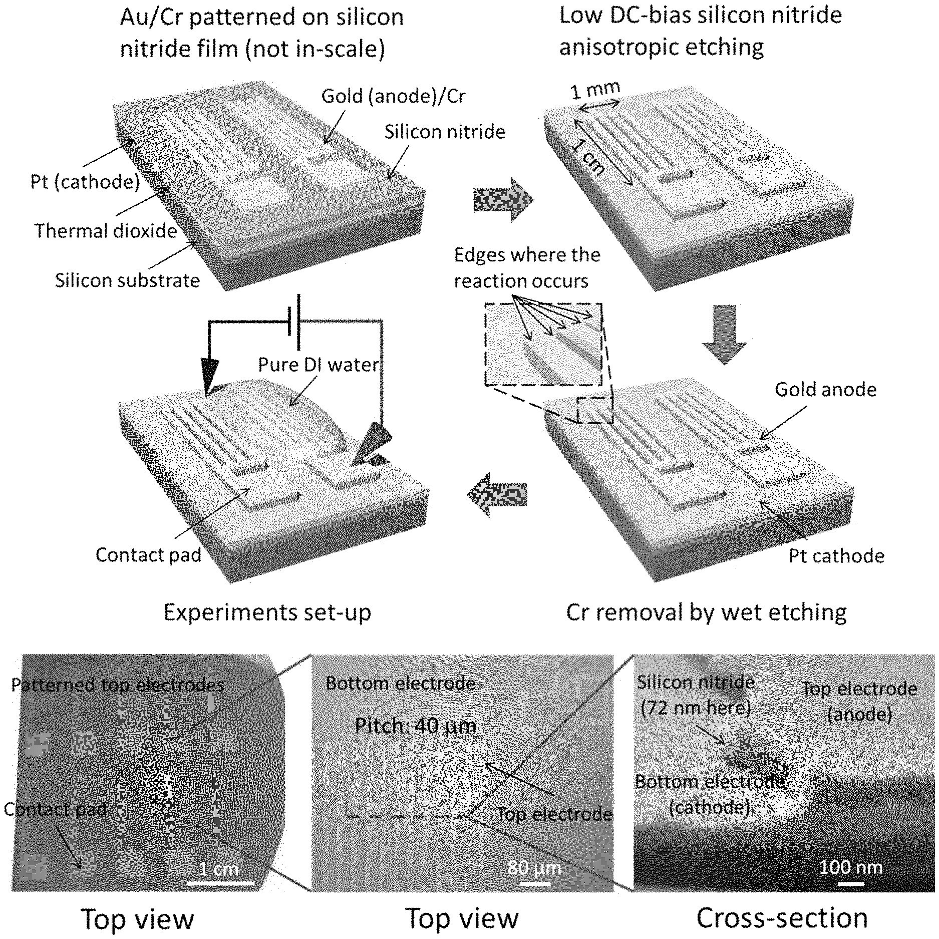
The fabrication process is shown in FIG. 2A-FIG. 2D. First, cathode metal (Ti/Pt) was deposited on thermally grown silicon dioxide by e-beam evaporation. Then silicon nitride was deposited by PECVD (FIG. 2A), with thickness from 50 nm to 500 nm. The anode (Ti/Au or Ni) was fabricated using photolithography, e-beam evaporation and lift-off (FIG. 2B). Eventually the silicon nitride layer was etched with anode metal as etching mask (FIG. 2C), and by using low-DC bias ME process, which could avoid short-circuit between cathode and anode metal layers due to the sputtering and deposition of metal on the sidewall of the silicon nitride spacer. The fabrication result is shown in FIG. 2D.
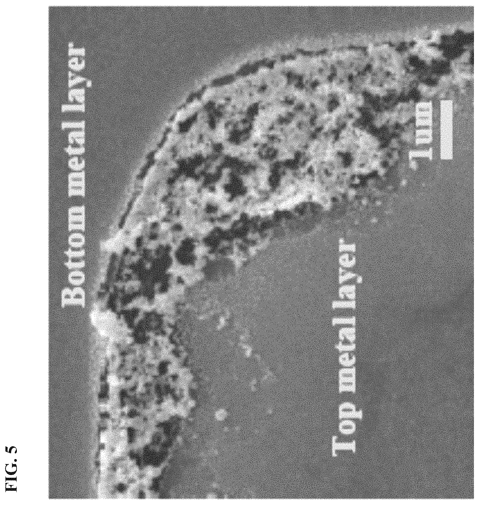
Bubbles were generated during water electrolysis based on our devices (FIG. 3). FIG. 4A shows the results of I-V curves measurement from the samples with the same pattern but different thickness of silicon nitride (i.e. different distances between electrodes). We found that when silicon nitride is thicker the threshold voltage is larger. This means the method to decrease the distance between two electrodes could reduce the external power as expected. When the distance between two electrodes is 50 nm the threshold voltage is 1.55V, which is almost the same as the theoretical limit of 1.47 V. FIG. 4B shows the results from the samples with the same thickness of silicon nitride but different grating pitches of the pattern. It indicates that the current increases linearly as the total number of edges of the gratings increases. However, in experiments we found that both Ni and Ti/Au as anodes would be corroded (FIG. 5) during water splitting, which will lead to short-circuit between electrodes. We determined that reliability can be improved by replacing the metal by indium tin oxide (ITO) or coating one ultrathin layer of dielectric for anode protection.
Example 2. Low DC-Bias Silicon Nitride Anisotropic Etching
Silicon nitride is one of the most important materials in micro/nanofabrication and applications, including diffusion barriers, etching mask material, electric insulators, etc. It has not only very excellent chemical inertia but also very high electrical resistivity. Particularly, metalinsulatormetal (MIM) sandwiched-like structures with silicon nitride as a dielectric layer have drawn a great deal of attention because of their numerous applications in MEMS switches, optical devices (e.g., metamaterials), biochemical sensing, and nanoelectronics.
However, it is hard to pattern silicon nitride by common reactive ion etch (ME) without causing short-circuit between the two metal layers in MIM sandwiched-like structures due to metal sputtered out and redeposited onto the sidewall.
Commonly used RIE methods usually take advantages of high DC-bias (self-bias) voltage to achieve perfect anisotropic etching profile. However, as shown in FIG. 29, high energy ions will bombard the top and bottom metal layers during etching process when DC-bias is high, resulting in metal atoms sputtered out everywhere and then redeposited back onto the substrate. In some cases, especially when the silicon nitride layer is very thin, those metal atoms will be unfortunately redeposited onto the sidewall of silicon nitride and form an electrical current path, in other words, short-circuit between two metal layers. Chromium is one of the most widely used materials as metal etching mask. However, theoretical analysis indicates that the sputtering yield of chromium will be up to 0.3 atoms/ion under bombardment of only 100 eV Argon.sup.+ ions. Moreover, most other metals have even higher sputtering yield. That is to say, it is very easy to sputter the metal atoms out to get short-circuit during common ME process. Wet etching of silicon nitride by hot phosphoric acid would not have such problems; however, it is isotropic and could not be utilized in some cases when vertical sidewalls are desired.
Although researchers have come up with many approaches to try to reduce the sputtering/redeposition during etching processes, such as modified gas combination, geometry and material optimization, and pressure modulation, there is no report yet applicable for particular etching methods for MIM sandwiched-like structures, especially when dielectric layer is very thin and low DC-bias is necessary. Here, we studied four factors that can affect the DC-bias and etching profile significantly: capacitively coupled RF power, inductively coupled plasma (ICP) power, the pressure in the etching chamber, and the combination of etching gases. Finally, we developed an excellent etching recipe for silicon nitride with only SF.sub.6 and C.sub.4F.sub.8 as etching gases. The DC-bias was lowered to only 34 V, and the sidewall is nearly vertical, with etching rate of 40 nm/min.
Further our study also showed that this recipe could avoid shortcircuit between two metal layers effectively.
Sample Preparation
The samples used to test silicon nitride etching recipes were fabricated by common semiconductor processes. As shown in FIG. 30A-FIG. 30F, first, 400 nm silicon nitride (SiNx) was deposited onto silicon wafers by plasma-enhanced chemical vapor deposition at 275 C. Then, photolithography, e-beam evaporation, and lift-off processes were used to define 30 nm thick chromium gratings on top of the deposited SiNx film, which were used as etching mask to test etching profiles. FIG. 31 shows a piece of sample prepared for etching recipe test.
Etching Test and Analysis
In general, both physical etching and chemical etching are exploited during dry etching processes, to keep balance between vertical profile and high selectivity. In experiments, we used only SF.sub.6 and C.sub.4F.sub.8 (and sometimes O.sub.2) as etching gases. SF.sub.6 was mainly used to generate F and SF.sub.x free radicals to etch SiN.sub.x, while C.sub.4F.sub.8 was the source of carbon-based passivation layer to protect the sidewall from etching (sometimes, O.sub.2 was used to adjust the C/F ratio slightly). In order to reduce the physical bombardment etching, and hence the sputtering of metal layer, we did not use argon as etching gas.
Two key points of etching recipes were investigated: first is the DC-bias, which should be low enough to reduce the sputtering yield; second is the etching profile, which should have vertical sidewalls as desired. There is a trade-off between those two, because it is difficult to generate vertical sidewalls with low DC-bias, in which physical bombardment is very weak; therefore, isotropic chemical etching is dominant.
One thing needs to be clarified: due to the collisions and scatterings of the ions from gas molecules (and ions) in the chamber, the kinetic energy of the bombardment ions is not necessarily the same as the DC-bias times the charge. But the kinetic energy is not directly measurable in contrary to the DC-bias, and DC-bias and the bombardment energy are closely correlated, so we studied the DC-bias instead. By carefully controlling the parameters of etching recipes, passivation and etching will be in dynamic equilibrium at the sidewalls, and therefore, vertical sidewalls can be achieved even when DC-bias is very low.
Four factors were studied: capacitively coupled RF power, ICP power, pressure in the etching chamber, and combination of etching gases. Each of them will affect the DC-bias and the etching profile significantly; even sometimes, the effects are coupled and not simply monotonous. Here, we tried different etching recipes with the same etching time of 5 min, and observed the DC-bias variation and the final etching profiles. The original silicon nitride layer was 400 nm, and the RIE etcher was Oxford Plasmalab system 100.
Capacitively Coupled RF Power
FIG. 32 shows the relationship between DC-bias and capacitively coupled RF power (or "RF power" abbreviated herein). When RF power increases, DC-bias increases monotonically. However, there is a striking RF power below which the DC-bias keeps at zero. At this striking threshold, DC-bias is not stable and could be either very high or zero. However, once the DC-bias has been activated, it is maintained easily. When the pressure is low enough, it is easier for striking because the mean-free-path gets larger so electrons can accumulate enough energy to excite the gas molecules. And also, when ICP power is higher, the striking RF power needed is smaller because ICP power increases the plasma density.
Moreover, we discovered that it is difficult to find low DC-bias recipe at high pressure. Experiments showed that the minimum DC-bias with struck plasma at high pressure is very large. FIG. 32 shows two SEM images at relatively low DC-bias (15 and 25 V, respectively). The one with lower RF power had lower DC-bias, and correspondingly achieved lower etching rate and more isotropic etching profile due to lower ion energy to remove the passivation layer and enhance the chemical etching rate at the bottom.
ICP Power
The relationship between DC-bias and ICP power is shown in FIG. 33. The circle line shows that DC-bias first turns on suddenly (the plasma strikes) and then decreases slowly along with ICP power increasing. The turn-on points are when the ionization rate is sufficient to compensate the electron loss (the triangle line only shows the data after its turn-on point and the square line only shows the data before its turn-on point). The turn-on points increase if the pressure increases, because mean-free-path gets shorter so more power are necessary to generate sufficient ionization rate. After the turn-on points, increasing ICP power results in larger plasma density, so the ion flow current toward the substrate increases. At fixed RF power, the product of ion flow current and bias voltage between two capacitive plates is conserved, therefore larger ICP power will lead to lower DC-bias.
Two SEM images from the circle line and the square line in FIG. 33 show nonetching results when the values of the ICP power are smaller than the turning points. The etching rate is almost zero even at high DC-bias because the plasma density is insufficient to generate enough radicals and to etch efficiently. Comparison within three SEM images from the triangle line indicates that ICP power affects the etching rate significantly: larger ICP power leads to faster etching. However, larger ICP power may not be a good choice even it will decrease the DC-bias, because lateral etching will also become faster so that the profile will become even more isotropic.
Pressure
The relationship between DC-bias and the pressure in the chamber is shown in FIG. 34. At low pressure, DC-bias increases as the pressure increases, which may result from increasing amount of charged particles (ions and electrons). However, we also discovered that at high pressure, DC-bias decreases as the pressure increases due to shorter mean-freepath. We also found that at very high pressure, the etching rate is much slower, which results from insufficient kinetic energy of the ions at high pressure with the fixed RF power and ICP power. When the pressure is too high (e.g., 50 mTorr), in fact, the plasma is difficult to be struck and the DC-bias keeps zero when RF power is relatively low. People have discovered that, low pressure can avoid etching product substrate redeposition and also may reduce the negative taper angle for trench etching. Therefore, here low pressure is our primary selection for low DC-bias etching.
Etching Gas Combinations
When the total flow rate is constant and the pressure is low, DC-bias decreases as C-to-F ratio increases, as shown in FIG. 35. That may be because carbon atoms are easier to be ionized than fluorine atoms; therefore, the gas in the chamber is more conductive with increasing C-to-F ratio. Another reason may be the electronic attachment of fluorine plasma, in which F ions tend to catch electrons to form F.sup.- ions. This leads to less free electron density between the capacitive plates then higher DC-bias voltage. While at high pressure, the DC-bias can either increase or decrease along with the increasing C-to-F ratio, depending on different recipes. The C-to-F ratio only plays a big role on the etching profile, coupled with the effect by DC-bias.
Beaklike Structures
In experiments, we discovered interesting beaklike structures formed at the top edge of silicon nitride at certain conditions, as shown in FIG. 36B. This is because the RF matching network tuning period sometimes can last up to several tens of seconds. During that time, the etching is mainly isotropic chemical etching because the reflected power is very high so the DC-bias is very low. When the tuning network gets matched, the DC-bias increases very fast to its stable value, after which there is more physical bombardment due to large DC-bias, and the etching profile goes back to normal. FIG. 36A shows a typical DC-bias matching period versus time.
The beaklike structures only occur when it takes a long time to tune the RF matching network. These initial striking periods are related to the etching recipes, and generally higher RF power, lower pressure, and higher final stable DC bias give shorter initial striking periods. We also discovered that more conductive substrates will reduce the initial striking periods significantly.
High-Performing Etching Recipe
By meticulously controlling the parameters of etching recipes, we eventually found a recipe with DC-bias of only 34V and nearly 90.degree. sidewall, as shown in FIG. 37, and the etching rate is 40 nm/min, which is fast enough for etching thin silicon nitride film in nanometer scale. The parameters are shown in Table 1 (FIG. 39). Moreover, further study shows that the selectivity between silicon nitride and chromium based on our optimal recipe is larger than 100:1.
More significantly, our experiments show that this recipe can be used to fabricate MIM sandwiched-like structures without causing short circuit between top and bottom metal layers. The cross section of one of the testing samples is shown in FIG. 38B, which has two 30 nm thick chromium layers and one 50 nm thick silicon nitride layer in between. The samples were tested under a common silicon nitride dry etching recipe with DC-bias of around 300V and our optimal recipe with DC-bias of only 34V for comparison. By measuring the resistances between each top Cr pad electrode and the bottom Cr layer electrode (FIG. 38A), we approved that our recipe can avoid short-circuit nearly 100% between two metal layers (resistances out of the range of our multimeter) while the common recipe always leads to short-circuit (smaller than 100.times.) between almost all the pad electrodes and the bottom metal layer.
Summary
In this paper, we provide a high-performing recipe for silicon nitride etching, with DC-bias of only 34 V, which prevents short circuits in fabricated MIM structures, and nearly 90.degree. etching sidewalls. The four main factors, capacitively coupled RF power, ICP power, the pressure in the etching chamber, and the combination of etching gases, have been studied to achieve low DC-bias and desired etching profiles. We discovered that the beaklike structures formed on the top edge of silicon nitride layer due to initial striking periods at certain etching conditions, which could be promising functional structures for some applications. The relationships between the four factors and etching results we discussed here can applied not only on silicon nitride, but also many other materials.
Example 3a (Part 1)
Due to the low conductivity of pure water, using an electrolyte is common for achieving efficient water electrolysis. In the present invention, we provide, in various embodiments a system for the electrolysis of pure water (without any added electrolyte) using deep-sub-Debye-length nanogap electrochemical cells. At such nanometer scale, the field-driven pure water splitting exhibits a completely different mechanism from the macrosystem. We have named this process "virtual breakdown mechanism" that results in a series of fundamental changes and more than 10.sup.5-fold enhancement of the equivalent conductivity of pure water. This fundamental discovery has been theoretically discussed in this paper and experimentally demonstrated in a group of electrochemical cells with nanogaps between two electrodes down to 37 nm. Based on our nanogap electrochemical cells, the electrolysis current from pure water is comparable to or even larger than the current from 1 mol/L sodium hydroxide solution, indicating the high-efficiency of pure water splitting as a potential for on-demand hydrogen production.
We have demonstrated a new approach to improve the electrochemical reaction efficiency, by using electrochemical cells with distance between anode and cathode in nanometer-scale. With these nanogap electrochemical cells (NECs), pure water (without any added electrolyte) can be electrochemically split into hydrogen and oxygen efficiently, in contrary to the traditional thinking that pure water cannot be electrolyzed. Our experiments have demonstrated that the equivalent conductivity of pure water has been enhanced more than 10.sup.5-fold, and the performance of NECs with pure water can be comparable to or even better than with 1 mol/L sodium hydroxide solution, which results from a completely different microscopic mechanism of field-driven ions transport to enhance water ionization and even virtual breakdown. Compared to current industrial water electrolysis operated at 70-90.degree. C. [2, 3] with strong alkaline electrolyte, our NEC design with pure water can eliminate difficulties of working with strong alkaline electrolyte and also avoid the need for high temperatures, showing a great potential for high energy-efficiency on-demand hydrogen production for both mass manufacturing and portable devices.
For simplicity, consider the solution resistance between anode and cathode for water splitting, as given by
.rho..times. ##EQU00001## where .rho. is the resistivity, l is the resistor length (electrode distance) and S is the cross-section area of the resistor. We found that as the electrode distance shrinks to much smaller than Debye-length .lamda.d (around 1 .mu.m for pure water), not only the value of l decreases, the equivalent resistivity .rho. decreases greatly as well, which in fact contributes more to the decrease of resistance R. This is attributed to the huge electric field between two electrodes within such deep-sub-Debye-length region (FIG. 40A-FIG. 40B). For water electrolysis with strong electrolyte in macrosystem, the electric field is screened by the double layer, leading to nearly zero electric field in bulk solution (FIG. 40A). However, when the electrode gap distance is smaller than the Debye-length, large electric field can be uniformly distributed in the entire gap due to overlapping of the double layers at the two electrodes. In our metal-dielectric-metal sandwiched-like NECs, the gap distance is tuned by adjusting the silicon nitride thickness and can be easily achieved to deep-sub-Debye-length in pure water. FIG. 40B shows the simulation results of electric field distribution between two electrodes with different gap distances. Close to the electrode regions both the nanogap cell and the macrosystem present a high electric field due to the double layer; however, in bulk solution the electric field in 100 .mu.m macrosystem is only 10 V/m while in 0.1 .mu.m gap the field can obtain 10.sup.7 V/m. Such a high electric field in the entire gap of nanogap cells can result in significant ion enrichment and ion migration [18, 19], and even further water ionization and virtual breakdown. Theoretical Analysis
FIG. 41A explains why pure water cannot be split efficiently in macrosystem, in which we take cathode and H3O.sup.+ ions as an example. Initially near the cathode surface water molecules can be dissociated into H3O.sup.+ and OH.sup.- ions. H3O.sup.+ ions obtain electrons from cathode leading to hydrogen evolution, while the newly-generated OH.sup.- ions can be transported very slowly through the bulk solution by slow diffusion or hopping process facilitated by a weak electric field in bulk solution. Moreover, the intrinsic concentration of H3O.sup.+ ions in bulk solution of pure water is too low to neutralize the OH.sup.- ions produced near the cathode. These lead to local OH.sup.- ions accumulation (so that the solution near cathode turns alkaline) especially at the cathode surface, causing the potential at the Helmholtz plane of the cathode to decrease (because of negatively-charged OH.sup.- ions). Such a potential decrease reduces the potential difference between the cathode and Helmholtz plane, further reducing the reaction rate of hydrogen evolution and thus water splitting. In other words, the reaction becomes very slow or even self-limited, showing a large equivalent resistance between cathode and anode. These phenomena also explain the rise in cathode overpotential, since a more negative cathode potential is necessary to allow the reaction to continue. The fundamental reason is the lack of rapid ions transport inside bulk solution.
When a high-concentration of sodium hydroxide is present in the electrolyte (FIG. 41B), plenty of Na.sup.+ ions from bulk solution can move to partially compensate for the charge from the newly-generated OH.sup.- ions near the cathode, restoring the potential difference between the cathode and Helmholtz plane, to reduce the overpotential requirement and sustain the reaction current. A similar process occurs at the anode. In this way, water electrolysis with strong electrolyte shows a small resistance between two electrodes. However, notice that even though the ions transport inside bulk electrolyte solution is large enough for the continued reaction, at cathode the sodium ions transport is still limited mainly by diffusion (because of weak electric field in bulk solution)[18, 20], which is often slower than OH.sup.- ions generation (i.e., reaction electron-transfer). Under steady-state conditions, net OH.sup.- ions accumulation still occurs at cathode and the potential effect on Helmholtz plane still exists.
In pure water, when the counter-electrode is placed within the Debye-length (FIG. 41C), the double layers of cathode and anode are overlapping with each other. Still at cathode, newly-generated OH.sup.- ions can be migrated rapidly from cathode towards anode due to large electric field in the entire gap. When the gap distance is small enough, initially the transport rate can be even higher than the electron-transfer rate. Once OH.sup.- ions are generated, they are immediately drawn from cathode to anode, resulting in the OH.sup.- ions waiting for electron-transfer at the anode, rather than accumulated at the cathode. The whole reaction would continue even in pure water, but now is limited by electron-transfer. In this case, net OH.sup.- ions accumulate near the anode and net H.sub.3O.sup.+ ions accumulate near the cathode, leading to completely opposite pH-value distribution compared to macrosystem (which maybe be good for protecting the anode against corrosion). Moreover, net OH.sup.- ion enrichment near the anode not only enhances the local reaction ions concentration but also increases the potential difference between anode and anode Helmholtz plane (which in fact decreases the overpotential requirement, as in the Frumkin effect[21]). According to Butler-Volmer equation [22],
.function..times..alpha..times..times..function.'.times..alpha..times..fu- nction.' ##EQU00002## such OH.sup.- ions accumulation can significantly increase the electrolysis current, namely water splitting throughput.
Under steady state, the field-driven effect is equivalent to the scenario that water molecules are split into H3O.sup.+ and OH.sup.- ions in the middle of the gap (FIG. 46), allowing H3O.sup.+ ions to drift towards the cathode and OH.sup.- ions to drift towards the anode, respectively. In other words, such huge electric field not only increases the transport rate, but also enhances the water molecules ionization (for RC-circuit model, FIG. 47). From a microscopic perspective, the conductivity of water has been enhanced "equivalently". From the equation of conductivity, .sigma.=nq.mu. (3) where q is the ion charge, .mu. is the ion mobility and n is the ion concentration. Here the ion charge s have not changed. The increased ion concentration only partially contributes to the conductivity. The fundamental change is that two half-reactions are coupled together, and the electric field distribution within the NEC gap leads to a significantly enhanced "apparent mobility". (In macro system, the intrinsic mobility cannot serve to the conductivity due to weak electric field in bulk solution.) The total effect looks like breakdown of pure water. However, notice that this effect is not traditional breakdown of pure water, which actually requires the electric field around 1 V/.ANG. [23], about two magnitude orders larger than what we have discussed here. The high electric field in our NECs could not split water molecules directly; however, it enhances water ionization and ion transport, and thus equivalent pure water conductivity. That is why we called this field-driven effect, "virtual breakdown mechanism". The traditional view should be revised that even pure water can be conductive, when the electrode gap is small enough. This "virtual breakdown mechanism" can be applied on almost all types of weakly-ionized materials: such weak ionization actually helps to achieve the virtual breakdown effect. Device Fabrication
There have been many efforts [24, 25] to fabricate nanogap electrodes.
Electron/ion-beam lithographically-defined nanogap electrodes may not be scalable to large-area fabrication.
Chemically-synthesized electrodes [26, 27] and mechanically-fabricated electrodes [28, 29] usually suffer from the lack of controllability. Sacrificial-layer based nanogaps [30-32] require complicated processes and thus perform poor yield[20] especially when nanogaps less than 100 nm. Bohn et al [18, 33, 34] and White et al [19, 20] have done excellent work on nanogap-based reversible redox cycling analysis at low ionic strength; however, their structures may not be suitable for irreversible reactions, especially with gas evolution. The fabrication procedure of our open-cell sandwiched-like NECs is shown in FIG. 42A. First, a film stack of silicon dioxide (thermal oxidation), Pt (bottom cathode metal, electron-beam evaporation), silicon nitride (plasma-enhanced chemical vapor deposition) were deposited on silicon wafers. Afterwards, Ti (adhesion layer) with gold (top anode metal) and Cr (etching mask) were patterned by photolithography, electron-beam evaporation and lift-off process. The patterns consist of contact pads and 1-D gratings with different values of pitch. Here only the top gold anode was patterned and the bottom Pt cathode was a blank film. Next, the silicon nitride was etched with Cr (low sputtering yield [35]) as mask by low DC-bias anisotropic etching that was developed by us [36], to avoid metal atoms sputtered out everywhere during etching. This method can avoid short-circuit between the top and bottom electrodes and thus enhance the yield of device fabrication. Finally, Cr mask was removed by Cr wet etching (ALDRICH.RTM.), which can also increase the hydrophilicity of the entire surface. The whole process is yield-controlled and can be scalable to mass manufacturing Platinum and gold were selected as the cathode and anode, respectively, due to their ability to catalyze hydrogen/oxygen evolution; gold is stable towards anodic oxidation [37] to avoid short-circuit between the two electrodes during electrolysis caused by metal dissolution and re-deposition [38]. The experimental set-up is schematically shown in FIG. 42A, with two electrode tips connected to the anode and cathode, and pure deionized water (DI water) was dropped to cover the grating region. The hydrophilicity of the entire surface guaranteed that the water completely wetted the whole electrode structure and gaps. Notice that the field-driven pure water splitting only occurs at the boundary (edges) of each grating line (more details in next section). FIG. 42B-FIG. 42D also shows the fabrication results (40 .mu.m g rating pitch and 72 nm gap distance as an example) observed by unaided eyes (top view), by optical microscopy (top view) and by scanning electron microscopy (SEM) (cross-section view).
Experimental Results
Pure Water
When exposed to air, CO.sub.2 dissolution into water (pH around 5.7 [39]) results in the Deby e-length reduction from 1 .mu.m to around 220 nm. For our smallest gap distance 37 nm, the double layer at each electrode has been at least compressed into 1/10 of the original Debye-length. At such deep-sub-Debye-length range, the uniform electric field in the entire gap is inversely proportional to the gap distance at a given voltage. FIG. 43A shows the I-V curves from pure water experiments based on different gap distances from 37 nm to 1.4 .mu.m. When gap distance shrank, the electrolysis current became larger due to higher electric field between two electrodes (FIG. 43A). A voltage plateau around 0.9 V was observed in the log current vs. voltage plot (FIG. 43B), which was independent of the gap distance. This may result from the dissolved oxygen reduction since the DI water was not saturated with inert gas; another reason may be surface oxide formation on gold during water electrolysis [38, 40, 41]. The entire surface became more hydrophilic after first test, which was consistent with the oxidation formation or hydroxide bond residue. In experiments, sometimes anode damage occurred when voltage was above 5 V (FIG. 49A-FIG. 49B). FIG. 43D shows part of the experimental set-up and bubbles generation around 2 V during the pure water splitting (FIG. 50A-FIG. 50B for more bubble effects). In NECs the electron-transfer rate only depends on the cell voltage while the transport rate (mainly by migration) depends both on voltage and gap distance (i.e., electric field). In a plot of electrolysis current vs. gap distance-1 (a scale of electric field) at each voltage, if the reaction is limited by electron-transfer, the current should be relatively independent of the gap distance; however, if the reaction is limited by mass transport, the current should be sensitive to the gap distance (showing a large slope). FIG. 43C clearly demonstrated such effects. For large gaps, a large slope appeared on the figure since the reaction was mass-transport limited; when the gap was small enough, the current reached saturation value only dependent on the voltage, indicating electron-transfer limited reaction. The critical gap distance (or "turning point") between such two states became smaller (moved to the right on the figure) with increasing voltage. This is because the electron-transfer rate increases faster than the mass transport when voltage increases (exponential vs. linear), therefore smaller gaps are necessary in order to achieve saturation current (electron-transfer limited) at higher voltages.
Sodium Hydroxide Solution
The electrolysis of pure water and 1 mol/L sodium hydroxide solution were compared in FIG. 44A, both based on our NECs with the same gap distance 72 nm and different grating pitches. For pure water, the electrolysis current at 1.8 V linearly increased with the number of grating edges; while for sodium hydroxide solution, the current was less dependent on the number of edges (i.e., grating pitch) and the data dispersion was significantly larger than that of pure water. The mechanism is shown in FIG. 44B. For pure water splitting, the reaction only occurs at the edges where the electrode distance is small enough to couple the two half-reactions together; at the "non-edge" region (i.e., top face) of the grating line, the scenario is just like pure water splitting in macrosystem (self-limited due to large electrode distance). On the contrary, in sodium hydroxide solution the entire surface was involved in supporting the reaction. That is because Debye-length in 1 mol/L sodium hydroxide solution is less than 1 nm, still significantly smaller than the electrode distance (72 nm here). Thus, the two half-reactions are not coupled together and are still diffusion-limited, just like that in macrosystem where the reactions occurs on all accessible parts of the electrodes. Therefore, the current greatly depends on the effective reaction area. In our present experiments, the area was that covered by the solution droplet and was not accurately controlled. Thus, the current from sodium hydroxide solution was not sensitive to grating pitches and presented significant variability (see more discussions in FIG. 51 A-FIG. 51B). In comparison, the current from pure water was not sensitive to the area of the droplet region, and bubbles could only form within the grating region. Also discussed herein are the two voltage plateaus around 0.4 V and 1.2 V, respectively, on the log-plot of the I-V curves in sodium hydroxide solution. Notice that the current from sodium hydroxide solution still increased slightly with the number of edges. Even though it was diffusion limited, at the edges the overall diffusion length had shrunk to 72 nm. Therefore more edges could slightly enhance the electrolysis current. Notice that the effective reaction area in sodium hydroxide solution was much larger than that in pure water. Even under such unfavorable conditions, the electrolysis current from pure water was comparable to that from 1 mol/L sodium hydroxide solution, indicating more than 10.sup.5-fold enhancement of the apparent conductivity of pure water. (The conductivity of 1 mol/L sodium hydroxide solution and common pure water (equilibrated with CO2 in air) are 2.times.10.sup.5 .mu.S/cm and 1 .mu.S/cm [39], respectively.) From the linear fitting, we can conclude that when the grating pitches are smaller than 2 .mu.m, the electrolysis current from pure water can be even higher than that from 1 mol/L sodium hydroxide solution of the same pitch (2 .mu.m pitch is beyond our photolithography capability, therefore we did not attempt it at present stage). These results demonstrate the enhancement of pure water splitting by virtual breakdown effect compared to conventional transport-limited reaction and a potential for greatly increased efficiency for hydrogen production.
Conclusion
Field-driven pure water splitting at room temperature has been successfully achieved in this paper based on our metal-dielectric-metal sandwiched-like nanogap electrochemical cells. The gap distance between anode and cathode down to 37 nm has been demonstrated. In such deep-sub-Debye-length region, high electric field in the entire gap significantly enhances water molecules ionization and mass transport, leading to an electron-transfer limited reaction. This virtual breakdown mechanism can greatly enhance the equivalent conductivity of pure water to more than 10.sup.5-fold, resulting in electrolysis current comparable to or even high than that from 1 mol/L sodium hydroxide solution, and thus a higher efficiency for hydrogen production. We propose to investigate this virtual breakdown mechanism further. For example, reference electrode can be added to study cathode current and anode current separately; characterizations of capacitance-voltage curves will also provide important information for theoretical analysis. Moreover, such virtual breakdown mechanism can be applied on almost all weakly-ionized materials, and may have applications for ultrafast charging, alcohol electrolysis, carbon-dioxide reduction and fuel cells. Besides, compared to other NECs, our open cells can be simply fabricated on large area with high yield, and have great potentials to enhance the rate of redox reactions for ultra-sensitivity/selectivity. At last, compared to current industrial water electrolysis, such high-efficiency pure water splitting without any electrolyte at room temperature, especially connected to renewable energy sources, is very promising for both mass manufacturing and portable devices for on-demand clean hydrogen production.
Example 3a (Part 2)
Finite Element Calculations
The simulation results shown in FIG. 40B were achieved using commercial software, Comsol Multiphysics.RTM. 5.2. The 2-D geometry and boundary conditions setting are shown in FIG. 45 (take gap distance of 5 .mu.m as an example, only one boundary edge of our sandwiched-like nanogap cells was simulated). The parameters setting are shown in Table Ia.
TABLE-US-00001 TABLE Ia Parameters setting in finite element calculations. Name Value Unit Description T0 25 deg C. Temperature c_H_bulk 0.0001 mol/m{circumflex over ( )}3 Bulk cation concentration c_OH_bulk c_H_bulk Bulk anion concentration z_H 1 Cation charge z_OH -1 Anion charge D_H 9.31E-09 m{circumflex over ( )}2/s Diffusion coefficient, cation D_OH 5.26E-09 m{circumflex over ( )}2/s Diffusion coefficient, anion eps_H2O 80 Relative permittivity of water xS 0.2 nm Stern layer thickness phi_anode 0.5 V Anode potential rho_space F_const*(z_H*c_H + z_OH*c_OH) C/m.sup.3 Space charge density deltaphi phiM-phi V Electrode-OHP potential difference rho_surf epsilon0_const*eps_H2O*deltaphi/xS C/m.sup.2 Surface charge density phiM (at anode) phi_anode/2 V Anode potential phiM (at cathode) -phi_anode/2 V Cathode potential thk_nitride Manually setting .mu.m Thickness of silicon nitride layer
The equations that governed the ions movement and distribution were the steady-state Nernst-Planck equation and the Poisson equation, J.sub.i=-D.sub.i.gradient.C.sub.i-(z.sub.iF/RT)D.sub.iC.sub.i.gradient..p- hi. (S1) .quadrature..sup.2.phi.=-.rho./.epsilon..sub.r.epsilon..sub.0 (S2) where Ji, Di, Ci, and zi are the current density, diffusion coefficient, concentration and charge of species i, .phi. is the local electric potential, .rho. is the local net charge density in the solution, .epsilon.r is the static dielectric constant, .epsilon.0, F, R, and T are the permittivity of vacuum, Faraday constant, gas constant and temperature. To simplify the problem, .epsilon.r of pure water was set constant 80 in the entire solution even though near the electrode surface .epsilon.r can be reduced to less than 10 [1].
The Debye-length (around 1 .mu.m in pure water) was calculated from Gouy-Chapman theory, which requires infinite electrode plane and potential much smaller than 26 mV at room temperature. Simulation results showed that, even though our modeling could not satisfy the two requirements of Gouy-Chapman theory, the approximation value of 1 .mu.m could still be used since little difference showed up between the theoretical value (from the Gouy-Chapman theory) and simulated value (from the software simulation). Besides, the smallest nanogap between the two electrodes we achieved was 37 nm, which was much smaller than both theoretical value and simulated value. Thus, the claim of "deep-sub-Debye-length" is still valid. Stern layer had been considered in the initial setting; however, the final results had little dependence on with or without Stern layer setting. This is probably because the simulation mesh was not fine enough near the electrode surface. Mesh quality is a key factor of the simulation results. We discovered that finer mesh near the surface greatly enhanced the surface concentration (more obvious when large potential added). However, further finer meshing was not possible due to limited computational resources. Here, more accurate results might not be necessary. Quantitatively, we have demonstrated the double layer overlapping effect, and high electric field (just voltage divided by gap distance) uniformly distributed in the entire gap has been demonstrated as well. For our current research, we determined that these simulation results are sufficient.
Virtual Breakdown Effect.
For pure water splitting in nanogap cells, the two half-reactions are coupled together. Take the anode as an example. At the anode OH.sup.- ions (the reaction ions) come from two parts: one is from water ionization near the anode; the other part comes from the OH.sup.- ions migrated from the cathode to the anode. When the gap is small enough, migration rate can be larger than electron-transfer rate so that the reaction is limited by electron-transfer. Initially, 1 unit of electron-transfer leads to two units of OH.sup.- ions generation, resulting in non-consumed OH.sup.- ions accumulated near the anode. Such ions accumulation at the electrodes slows down further water ionization near the electrodes, to reduce the total OH.sup.- ions generation rate to balance with the 1 unit of electron-transfer in the external circuit. Under steady state condition, the sum of the OH.sup.- ions from the two parts is balanced with the 1 unit of electron-transfer in the external circuit. Such scenario appears like that the water molecules are split into H3O.sup.+ and OH.sup.- ions in the middle of the gap, allowing H3O.sup.+ ions to drift towards the cathode and OH.sup.- ions to drift towards the anode, respectively. The whole effect looks like that water has been broken-down. However, we should point out that in fact water molecule dissociation still occurs only near the electrode (due to local ion consumption); the water dissociation in the middle of the gap is just the equivalent effect.
RC-Circuit Model
FIG. 47 shows the RC-circuit model of half-reaction of water splitting in nanogap cells. The capacitor represents the double layer. R1 represents the reaction rate of electron-transfer, which depends only on the changes in potential drop across the interface. R2 represents the mass transport rate, which is related to both voltage and gap distance (i.e., electric field in the gap). R3 represents the water ionization rate. When gap distance is smaller, R2 becomes smaller; while R1 can also be slightly smaller since local reaction ion concentrations become higher and potential drop becomes larger, meaning that R1 is coupled to R2. R3 may depend on R1 because ions are consumed continuously, R3 can be enhanced by shifting the ionization equilibrium. When the gap distance is around Debye-length, R2 is the largest one and determines the whole reaction rate; however, when gap is much smaller than Debye-length, R2 can be smaller than R1, indicating electron-transfer limited reaction. That is to say, when gap distance further decreases, the current reaches a saturation value that only depends on voltage.
Low DC-Bias Silicon Nitride Anisotropic Etching.
To avoid short-circuit between top anode and bottom cathode metal layers, low DC-bias silicon nitride etching technology was developed in order to reduce the ion bombardment effect. In experiments we discovered that traditional nitride etching with high DC-bias could lead to low yield of device fabrication: most of the devices got short-circuit after nitride etching. This was because that the sputtered metal atoms formed short-circuit path on the sidewall, connecting top anode and bottom cathode [2]. By using our low DC-bias etching recipe, the fabrication yield has been improved greatly. The recipe parameters and the etching profile are shown in FIG. 48. The DC-bias of the silicon nitride etching was down to 19-21 V with etching rate larger than 80 nm/min and vertical sidewalls, even better than literature reported values [2]. Exactly vertical sidewalls were not required because in fact a little bit isotropic etching was desired since anode tips at the boundary could form higher electric field.
Anode Damage.
Anode can be roughed during redox cycling [3, 4]. The roughness comes from the electrochemically oxidation and re-deposition of the anode metal, even for gold [3, 5]. In experiments, such anode damage sometimes occurred when the applied voltage values were above 5 V (FIG. 49A-FIG. 49B). Thinner-gap samples were more likely to suffer damage. Moreover, damage always showed up near the grating boundary where the electric field was the highest. Such damage, especially the re-deposition of gold atoms, can lead to short-circuit between the anode and the cathode (especially for smaller gap distances), and thus reducing the lifetime of the devices. To avoid such short-circuit, the maximum external voltage was set to be 2.5 V (to reduce the current density in fact). In this way, the devices can be measured repetitively without obvious damage or short-circuit.
Two possible approaches are proposed here to avoid such anode damage. First, indium tin oxide (ITO) can be used to replace the gold as anode material, with its highest oxidation state which cannot be oxidized further [6, 7]. Second, an ultrathin layer of energy-band offset material [8, 9] may be coated onto the gold anode, with thickness small enough to be conductive to gold while preventing gold contacting water directly.
Bubble Effects
FIG. 50A-FIG. 50B shows plateaus (or peaks) around 2 V in I-V curves, both in pure water measurements and sodium hydroxide solution measurements. We believe that it was due to bubble effects. Around 2 V, bubble generation started to be vigorous enough so that it could be observed by the naked eye. Moreover, devices with smaller gap distance or smaller grating pitches could have more obvious plateaus around 2 V, indicating that such plateaus were determined by the geometry of the structures, rather than electrode electrochemical reactions. This observation is reasonable to expect since bubbles are more likely to be trapped within the smaller gap or smaller pitch structures before releasing, excluding the water involved in the reaction. Therefore, larger voltage leads to larger excluding effect, and thus smaller current, showing negative resistance which performs like a plateau or peak in I-V curves.
Notice that FIG. 50A also shows the consistent results among several tests. The data from different devices were almost exactly the same, especially below 2 V. Above 2 V, the data had a relatively larger error range which we think was due to the bubble effects on current performance. Therefore, we always selected the current data below 2V for analysis and comparison to be free from bubble related artifacts.
Sodium Hydroxide Solution: Reactions in the Entire Surface
Reactions in pure water only occur at the edge boundary of each grating line in our sandwiched-like nanogap cells. Different from pure water, the entire surface is involved in the reactions in sodium hydroxide solutions. Two types of evidence are shown in FIG. 51A-FIG. 51B. First, the larger droplet of sodium hydroxide solution provided larger current, indicating more surface area involved into the reactions, though the total number of the edges was independent of the droplet size. Second, bubbles could be even generated far away from counter-electrode (i.e., non-grating region), demonstrating that reactions can occur even very far from the grating edges. That is to say, the reactions in sodium hydroxide solutions not only occur at the grating edges, but also over the entire region covered by the droplet.
Plateaus in Log I vs. V Curves
FIG. 52A-FIG. 52B shows the log I vs. V curves from tests of both pure water and sodium hydroxide solution. For pure water, one plateau appeared around 0.9 V (also shown in FIG. 43B). This plateau became flatter after the first test on the same device. For sodium hydroxide solution, two plateaus, around 0.4 V and 1.2 V respectively, were shown on the log I vs. V curves. After first test, the 0.4 V plateau still existed but the 1.2 V plateau disappeared, and the current became much larger (the 2V plateau can be ignored since it is due to the bubble effects). This plateau phenomenon is quite repeatable, no matter what the gap distance or pitch is, indicating that it is more likely related to the intrinsic electrochemical reactions, rather than geometry factors. However, the fundamental mechanism is not clear.
Only a few literature reviews discussed about such plateaus in log I vs. V curves. Without being bound by theory, our hypothesis is the following. The 0.9 V plateau from pure water tests may be attributed to dissolved oxygen reduction or anode gold oxidation (and these two effects might be coupled). For sodium hydroxide solution, the 0.4 V plateau most likely came from the reduction of dissolved oxygen; while the 1.2 V plateau was related to anode gold oxidation. The different values of the oxidation plateaus in pure water and in sodium hydroxide solution was most likely due to the difference in pH values. The 0.4 V plateau would not disappear since for every test new sodium hydroxide solution (without inert gas saturation) was used. For the gold anode, non-conductive oxide state I and conductive oxide state II can form during water splitting [10]. During the first test in sodium hydroxide solution, OH.sup.- ions concentration was so large that all surface gold could be oxidized to state II, therefore during the second or third tests no surface gold could be oxidized further (thus the 1.2 V plateau disappeared). Also, because oxide state II was porous and conductive, the distance between anode and cathode had been shortened due to gold oxide islands and the current after the first test could become larger (the larger current could be also attributed to roughness of the surface since effective reaction area became larger [4]). However, for pure water, OH.sup.- ions concentration was small so that only oxide state I might form, therefore gold could still be oxidized further into the formation of state I during the second or even third tests (until two or three monolayers of the oxide state I coverage reached [3, 11]), with almost the same electrolysis current or smaller since oxide state I was non-conductive. However, such plateaus may also result from the formation of oxygen coverage [12], inhibition layer [13] or inert sites [14].
Example 3b (Part 1)
Due to the low conductivity of pure water, using an electrolyte is common for achieving efficient water electrolysis. In the present invention, we provide, in various embodiments a system for the electrolysis of pure water (without any added electrolyte) at room temperature with high efficiency using deep-sub-Debye-length nanogap electrochemical cells. A novel field-driven effect resulted from overlapped electrical double layers can significantly enhance water molecules ionization and mass transport, leading to electron-transfer limited reactions (which is completely different from traditional mechanisms). We have named this process "virtual breakdown mechanism" that couples the two half-reactions together, resulting in more than 10.sup.5-fold enhancement of the equivalent conductivity of pure water. This fundamental discovery has been theoretically discussed in this paper and experimentally demonstrated in a group of electrochemical cells with nanogaps between two electrodes down to 37 nm. Based on our nanogap electrochemical cells, the electrolysis current density from pure water can be significantly larger than that from 1 mol/L sodium hydroxide solution, indicating the high efficiency of pure water splitting as a potential for on-demand clean hydrogen production.)
We have demonstrated a new approach to improve the electrochemical reaction efficiency, by using electrochemical cells with distance between anode and cathode in nanometer-scale. With these nanogap electrochemical cells (NECs), pure water (without any added electrolyte) can be electrochemically split into hydrogen and oxygen efficiently due to the two half-reactions coupled together, contrary to the traditional thinking that pure water cannot be electrolyzed. Our experiments have demonstrated that the equivalent conductivity of pure water has been enhanced more than 10.sup.5-fold, and the electrolysis current density from pure water can be greatly larger than that from 1 mol/L sodium hydroxide solution, which results from a completely different microscopic mechanism of field-driven ions transport to enhance water ionization and even virtual breakdown. Compared to current industrial water electrolysis operated at 70-90.degree. C. [2, 3] with strong alkaline electrolyte, our NEC design with pure water can eliminate difficulties of working with strong alkaline electrolyte and also avoid the need for high temperatures, showing a great potential for high energy-efficiency on-demand hydrogen production for both mass manufacturing and portable devices.
For simplicity, consider the solution resistance between anode and cathode for water splitting, as given by
.rho..times. ##EQU00003## where .rho. is the resistivity, l is the resistor length (electrode distance) and S is the cross-section area of the resistor. We found that as the electrode distance shrinks to much smaller than Debye-length .lamda.d (around 1 .mu.m for pure water), not only the value of l decreases, but the equivalent resistivity .rho. also decreases greatly, which in fact contributes more to the decrease of resistance R. This decrease is attributed to the huge electric field between two electrodes within such deep-sub-Debye-length region (FIG. 40A-FIG. 40B). For water electrolysis with strong electrolyte in macrosystem, the electric field is screened by the double layer, leading to nearly zero electric field in bulk solution (FIG. 40A). However, when the electrode gap distance is smaller than the Debye-length, large electric field can be uniformly distributed in the entire gap due to overlapping of the double layers at the two electrodes. In our metal-dielectric-metal sandwiched-like NECs, the gap distance is tuned by adjusting the silicon nitride thickness and can be easily achieved to deep-sub-Debye-length in pure water. FIG. 40B shows the simulation results of electric field distribution between two electrodes with different gap distances. Close to the electrode regions both the nanogap cell and the macrosystem present a high electric field due to the double layer; however, in bulk solution the electric field in 100 .mu.m macrosystem is only 10 V/m while in 0.1 .mu.m gap the field can reach 10.sup.7 V/m. Such a high electric field in the entire gap of nanogap cells can result in significant ion enrichment and ion migration [18, 19], and even further water ionization and virtual breakdown. Theoretical Analysis.
FIG. 41A explains why pure water cannot be split efficiently in macrosystem, in which we take the cathode and H3O.sup.+ ions as an example. Initially near the cathode surface water molecules can be dissociated into H3O.sup.+ and OH.sup.- ions. H3O.sup.+ ions obtain electrons from the cathode leading to hydrogen evolution, while the newly-generated OH.sup.- ions can be transported very slowly through the bulk solution by slow diffusion or hopping processes facilitated by a weak electric field in bulk solution. Moreover, the intrinsic concentration of H3O.sup.+ ions in bulk solution of pure water is too low to neutralize the OH.sup.- ions produced near the cathode. These lead to local OH.sup.- ions accumulation (so that the solution near cathode turns alkaline) especially at the cathode surface, causing the potential at the Helmholtz-plane of the cathode to decrease (because of negatively-charged OH.sup.- ions). Such a potential decrease reduces the potential difference between the cathode and Helmholtz-plane, further reducing the reaction rate of hydrogen evolution and thus water splitting. In other words, the reaction becomes very slow or even self-limited, showing a large equivalent resistance between cathode and anode. These phenomena also explain the rise in cathode overpotential, since a more negative cathode potential is necessary to allow the reaction to continue. The fundamental reason is the lack of rapid ion transport inside bulk solution.
When a high-concentration of sodium hydroxide is present in the electrolyte (FIG. 41B), plenty of Na.sup.+ ions from bulk solution can move to partially compensate for the charge from the newly-generated OH.sup.- ions near the cathode, restoring the potential difference between the cathode and Helmholtz-plane, to reduce the overpotential requirement and sustain the reaction current. A similar process occurs at the anode. In this way, water electrolysis with strong electrolyte shows a small resistance between two electrodes. However, notice that even though the ion transport inside bulk electrolyte solution is large enough for the continued reaction, at cathode the sodium ions transport is still limited mainly by diffusion (because of the weak electric field in bulk solution)[18, 20], which is often slower than OH.sup.- ions generation (i.e., reaction electron-transfer). Under steady-state conditions, net OH-- ions accumulation still occurs at cathode and the potential effect on Helmholtz-plane still exists.
In pure water, when the counter-electrode is placed within the Debye-length (FIG. 41C), large electric field can form in the entire gap. When the gap distance is small enough, initially the transport rate can be even higher than the electron-transfer rate. Once OH.sup.- ions are generated at the cathode, they are immediately drawn from cathode to anode, resulting in the OH-ions waiting for electron-transfer at the anode, rather than accumulated at the cathode. The whole reaction would continue even in pure water, but now is limited by electron-transfer. In this case, net OH.sup.- ions accumulate near the anode and net H3O.sup.+ ions accumulate near the cathode, leading to completely opposite pH-value distribution compared to macrosystem (which may be good for protecting the anode against corrosion). Moreover, net OH.sup.- ion enrichment near the anode not only enhances the local concentration of the reactant ions but also increases the potential difference between anode and anode Helmholtz-plane (which in fact decreases the overpotential requirement, as in the Frumkin effect[21]). According to the Butler-Volmer equation [22],
.function..times..alpha..times..times..function.'.times..alpha..times..fu- nction.' ##EQU00004## such OH.sup.- ions accumulation can significantly increase the electrolysis current, namely water split ting throughput.
Under steady state, the field-driven effect is equivalent to the scenario that water molecules are split into H3O.sup.+ and OH.sup.- ions in the middle of the gap (see FIG. 46 for more explanations), allowing H3O.sup.+ ions to drift towards the cathode and OH.sup.- ions to drift towards the anode, respectively. In other words, such huge electric field not only increases the transport rate, but also enhances the water molecules ionization (for RC-circuit model, see FIG. 47). From a microscopic perspective, the conductivity of water has been enhanced "equivalently". From the equation of conductivity, .sigma.=nq.mu. (3) where q is the ion charge, .mu. is the ion mobility and n is the ion concentration. Here the ion charge s have not changed. The increased ion concentration only partially contributes to the conductivity. The fundamental change is that two half-reactions are coupled together, and the electric field distribution within the NEC gap leads to a significantly enhanced "apparent mobility". (In macro system, the intrinsic mobility cannot support the conductivity due to the weak electric field in bulk solution.) The total effect looks like breakdown of pure water. However, notice that this effect is not traditional breakdown of pure water, which actually requires the electric field around 1 V/.ANG. [23], about two magnitude orders larger than what we have discussed here. The high electric field in our NECs could not split water molecules directly; however, it enhances water ionization and ion transport, and thus equivalent pure water conductivity. That is why we called this field-driven effect, "virtual breakdown mechanism". The traditional view should be revised that even pure water can be conductive, when the electrode gap is small enough. This "virtual breakdown mechanism" can be applied on almost all types of weakly-ionized materials: such we ak ionization actually helps to achieve the virtual breakdown effect. Device Fabrication
There have been many efforts [24, 25] to fabricate nanogap electrodes. Electron/ion-beam lithographically-defined nanogap electrodes may not be scalable to large-area fabrication. Chemically-synthesized electrodes [26, 27] and mechanically-fabricated electrodes[28, 29] usually suffer from the lack of controllability. Sacrificial-layer based nanogaps [30-32] require complicated processes and thus perform poor yield [20] especially when nanogaps less than 100 nm. Bohn et al [18, 33, 34] and White et al [19, 20] have done excellent work on nanogap-based reversible redox cycling analysis at low ionic strength; however, their structures may not be suitable for irreversible reactions, especially with gas evolution.
The fabrication procedure of our open-cell sandwiched-like NECs is shown in FIG. 42A. First, a film stack of silicon dioxide (thermal oxidation), Pt (bottom cathode metal, electron-beam evaporation), silicon nitride (plasma-enhanced chemical vapor deposition) were deposited on silicon wafers. Afterwards, Ti (adhesion layer) with gold (top anode metal) and Cr (etching mask) were patterned by photolithography, electron-beam evaporation and lift-off process. The patterns consist of contact pads and 1-D gratings with different values of pitch. Here only the top gold anode was patterned and the bottom Pt cathode was a blank film. Next, the silicon nitride was etched with Cr (low sputtering yield[35]) as mask by low DC-bias anisotropic etching that was developed by us[36], to avoid metal atoms sputtered out everywhere during etching. This method can avoid short-circuit between the top and bottom electrodes and thus enhance the yield of device fabrication. Finally, the Cr mask was removed by Cr wet etching (ALDRICH.RTM.), which can also increase the hydrophilicity of the entire surface. The whole process is yield-controlled and can be scalable to mass manufacturing.
Platinum and gold were selected as the cathode and anode, respectively, due to their ability to catalyze hydrogen/oxygen evolution; gold is stable towards anodic oxidation [37] to avoid short-circuit between the two electrodes during electrolysis caused by metal dissolution and re-deposition [38]. The experimental set-up is schematically shown in FIG. 42A, with two electrode tips connected to the anode and cathode, and pure deionized water (DI water) was dropped to cover the grating region. The hydrophilicity of the entire surface guaranteed that the water completely wetted the whole electrode structure and gaps. Notice that the field-driven pure water splitting only occurs at the boundary (edges) of each grating line (more details in next section). FIG. 42B-FIG. 42D also shows the fabrication results (40 .mu.m grating pitch and 72 nm gap distance as an example) observed by unaided eyes (top view), by optical microscopy (top view) and by scanning electron microscopy (SEM) (cross-section view).
Experimental Results
Pure Water.
When exposed to air, CO.sub.2 dissolution into water (pH around 5.7 [39]) results in the Debye-length reduction from 1 .mu.m to around 220 nm. For our smallest gap distance 37 nm, the double layer at each electrode has been at least compressed into 1/10 of the original Debye-length, as we claimed "deep-sub-Debye-length". FIG. 43A shows the I-V curves from pure water experiments based on different gap distances from 37 nm to 1.4 .mu.m. When gap distance shrank, the electrolysis current became larger due to higher electric field between two electrodes (FIG. 43A). The threshold voltage around 1.5 V suggests that the energy efficiency is very close to 100% based on a thermoneutral potential of 1.48 V [5]. A voltage plateau around 0.9 V was observed in the log current vs. voltage plot (FIG. 43B), which was independent of the gap distance. This may result from the dissolved oxygen reduction since the DI water was not saturated with inert gas; another reason may be surface oxide formation on gold during water electrolysis [38, 40, 41]. The entire surface became more hydrophilic after first test, which was consistent with surface oxidation or hydroxide formation. In experiments, sometimes anode damage occurred when the voltage was above 5 V (see FIG. 49A-FIG. 49B). FIG. 43D shows part of the experimental set-up and bubbles generation around 2 V during the pure water splitting (see FIG. 50A-FIG. 50B for more bubble effects).
In NECs the electron-transfer rate only depends on the cell voltage while the transport rate (mainly by migration) depends both on voltage and gap distance (i.e., electric field). In a plot of electrolysis current vs. gap distance-1 (a scale of electric field) at each voltage, if the reaction is limited by electron-transfer, the current should be relatively independent of the gap distance; however, if the reaction is limited by mass transport, the current should be sensitive to the gap distance (showing a large slope). FIG. 43C clearly demonstrated such effects. For large gaps, a large slope appeared on the figure since the reaction was mass-transport limited; when the gap was small enough, the current reached saturation value only dependent on the voltage, indicating an electron-transfer limited reaction. The critical gap distance (or "turning point") between such two states became smaller (moved to the right on the figure) with increasing voltage. This is because the electron-transfer rate increases faster than the mass transport when voltage increases (exponential vs. linear), therefore smaller gaps are necessary in order to achieve saturation current (electron-transfer limited) at higher voltages.
Sodium Hydroxide Solution.
The electrolysis of pure water and 1 mol/L sodium hydroxide solution were compared in FIG. 44A, both based on our NECs with the same gap distance 72 nm and different grating pitches. For pure water, the electrolysis current at 1.8 V linearly increased with the number of grating edges; while for sodium hydroxide solution, the current was less dependent on the number of edges (i.e., grating pitch) and the data dispersion was significantly larger than that of pure water. The mechanism is shown in FIG. 44B. For pure water splitting, the reaction only occurs at the edges where the electrode distance is small enough to couple the two half-reactions together; at the "non-edge" region (i.e., top face) of the grating line, the scenario is just like pure water splitting in macrosystem (self-limited due to large electrode distance). On the contrary, in sodium hydroxide solution the entire surface was involved in supporting the reaction. That is because Debye-length in 1 mol/L sodium hydroxide solution is less than 1 nm, still significantly smaller than the electrode distance (72 nm here). Thus, the two half-reactions are not coupled together and are still diffusion-limited, just like that in macrosystem where the reactions occurs on all accessible parts of the electrodes. Therefore, the current greatly depends on the effective reaction area. In our present experiments, the area was that covered by the solution droplet and was not accurately controlled. Thus, the current from sodium hydroxide solution was not sensitive to grating pitches and presented significant variability (see more discussions in FIG. 51A-FIG. 51B). In comparison, the current from pure water was not sensitive to the area of the droplet region, and bubbles could only form within the grating region. Also discussed here in are the two voltage plateaus around 0.4 V and 1.2 V, respectively, on the log-plot of the I-V cu ryes in sodium hydroxide solution.
Notice that the current from sodium hydroxide solution still increased slightly with the number of edges. Even though it was diffusion limited, at the edges the overall diffusion length had shrunk to 72 nm. Therefore, more edges could slightly enhance the electrolysis current. Notice that the effective reaction area in sodium hydroxide solution was much larger than that in pure water. Even under such unfavorable conditions, the electrolysis current from pure water was comparable to that from 1 mol/L sodium hydroxide solution, indicating much larger current density from pure water and more than 10.sup.5-fold enhancement of the apparent conductivity of pure water. (The conductivity of 1 mol/L sodium hydroxide solution and common pure water (equilibrated with CO.sub.2 in air) are 2.times.10.sup.5 .mu.S/cm and 1 .mu.S/cm [39], respectively.) From the linear fitting, we can conclude that when the grating pitches are smaller than 2 .mu.m, the electrolysis current from pure water can be even higher than that from 1 mol/L sodium hydroxide solution of the same pitch (2 .mu.m pitch is beyond our photolithography capability, therefore we did not attempt it at present stage). These results demonstrate the enhancement of pure water splitting by virtual breakdown effect compared to the conventional transport-limited reaction and a potential for greatly increased efficiency for hydrogen production.
Conclusion
Field-driven splitting of pure water at room temperature for high-efficiency hydrogen production has been successfully achieved in this paper based on our metal-dielectric-metal sandwiched-like nanogap electrochemical cells. The gap distance between anode and cathode down to 37 nm has been demonstrated. In such deep-sub-Debye-length region where double layers overlapped, high electric field in the entire gap couples the two half-reactions together, and significantly enhances water molecules ionization and mass transport, leading to an electron-transfer limited reaction. This virtual breakdown mechanism can greatly enhance the equivalent conductivity of pure water by more than 10.sup.5-fold, resulting in electrolysis current density significantly larger than that from 1 mol/L sodium hydroxide solution, and thus a higher efficiency for hydrogen production. We propose to investigate this virtual breakdown mechanism further. For example, reference electrode can be added to study cathode current and anode current separately; characterizations of capacitance-voltage curves will also provide important information for theoretical analysis. Moreover, such virtual breakdown mechanism can be applied on almost all weakly-ionized materials, and may have applications for ultrafast charging, alcohol electrolysis, carbon-dioxide reduction and fuel cells. Besides, compared to other NECs, our open cells can be simply fabricated on large area with high yield, and have a great potential to enhance the rate of redox reactions for ultra-sensitivity/selectivity. At last, compared to the current industrial water electrolysis, such high-efficiency pure water splitting without any electrolyte at room temperature, especially connected to renewable energy sources, is very promising for both mass manufacturing and portable devices for on-demand clean hydrogen production.
Example 3b (Part 2)
Finite Element Calculations
The simulation results shown in FIG. 40B were achieved using commercial software, Comsol Multiphysics.RTM. 5.2. The 2-D geometry and boundary conditions setting are shown in FIG. 45 (take gap distance of 5 .mu.m as an example, only one boundary edge of our sandwiched-like nanogap cells was simulated). The parameters setting are shown in Table Ib.
TABLE-US-00002 TABLE Ib Parameters setting in finite element calculations. Name Value Unit Description T0 25 deg C. Temperature c_H_bulk 0.0001 mol/m{circumflex over ( )}3 Bulk cation concentration c_OH_bulk c_H_bulk mol/m{circumflex over ( )}3 Bulk anion concentration z_H 1 Cation charge z_OH -1 Anion charge D_H 9.31E-09 m{circumflex over ( )}2/s Diffusion coefficient, cation D_OH 5.26E-09 m{circumflex over ( )}2/s Diffusion coefficient, anion eps_H2O 80 Relative permittivity of water xS 0.2 nm Stern layer thickness phi_anode 0.5 V Anode potential rho_space F_const*(z_H*c_H + z_OH*c_OH) C/m.sup.3 Space charge density deltaphi phiM-phi V Electrode-OHP potential difference rho_surf epsilon0_const*eps_H2O*deltaphi/xS C/m.sup.2 Surface charge density phiM (at anode) phi_anode/2 V Anode potential phiM (at cathode) -phi_anode/2 V Cathode potential thk_nitride Manually setting .mu.m Thickness of silicon nitride layer
The equations that governed the ions movement and distribution were the steady-state Nernst-Planck equation and the Poisson equation, J.sub.i=-D.sub.i.gradient.C.sub.i-(z.sub.iF/RT)D.sub.iC.sub.i.gradient..p- hi. (S1) .quadrature..sup.2.phi.=-.rho./.epsilon..sub.r.epsilon..sub.0 (S2) where Ji, Di, Ci, and zi are the current density, diffusion coefficient, concentration and charge of species I, .phi. is the local electric potential, .rho. is the local net charge density in the solution, .epsilon.r is the static dielectric constant, .epsilon.0, F, R, and T are the permittivity of vacuum, Faraday constant, gas constant and temperature. To simplify the problem, .epsilon.r of pure water was set constant 80 in the entire solution even though near the electrode surface .epsilon.r can be reduced to less than 10 [1].
The Debye-length (around 1 .mu.m in pure water) was calculated from Gouy-Chapman theory, which requires infinite electrode plane and potential much smaller than 26 mV at room temperature. Simulation results showed that, even though our modeling could not satisfy the two requirements of Gouy-Chapman theory, the approximation value of 1 .mu.m could still be used since little difference showed up between the theoretical value (from the Gouy-Chapman theory) and simulated value (from the software simulation). Besides, the smallest nanogap between the two electrodes we achieved was 37 nm, which was much smaller than both theoretical value and simulated value. Thus, the claim of "deep-sub-Debye-length" is still valid.
Stern layer had been considered in the initial setting; however, the final results had little dependence on with or without Stern layer setting. This is probably because the simulation mesh was not fine enough near the electrode surface. Mesh quality is a key factor of the simulation results. We discovered that finer mesh near the surface greatly enhanced the surface concentration (more obvious when large potential added). However, further finer meshing was not possible due to limited computational resources. Here, more accurate results might not be necessary. Quantitatively, we have demonstrated the double layer overlapping effect, and high electric field (just voltage divided by gap distance) uniformly distributed in the entire gap has been demonstrated as well. For our current research, we determined that these simulation results are sufficient.
Virtual Breakdown Effect
For pure water splitting in nanogap cells, the two half-reactions are coupled together. Take the anode as an example. At the anode OH-- ions (the reaction ions) come from two parts: one is from water ionization near the anode; the other part comes from the OH.sup.- ions migrated from the cathode to the anode. When the gap is small enough, migration rate can be larger than electron-transfer rate so that the reaction is limited by electron-transfer. Initially, 1 unit of electron-transfer leads to two units of OH.sup.- ions generation, resulting in non-consumed OH.sup.- ions accumulated near the anode. Such ions accumulation at the electrodes slows down further water ionization near the electrodes, to reduce the total OH.sup.- ions generation rate to balance with the 1 unit of electron-transfer in the external circuit. Under steady state condition, the sum of the OH.sup.- ions from the two parts is balanced with the 1 unit of electron-transfer in the external circuit. Such scenario appears like that the water molecules are split into H3O.sup.+ and OH.sup.- ions in the middle of the gap (FIG. 46), allowing H3O.sup.+ ions to drift towards the cathode and OH.sup.- ions to drift towards the anode, respectively. The whole effect looks like that water has been broken-down. However, we should point out that in fact water molecule dissociation still occurs only near the electrode (due to local ion consumption); the water dissociation in the middle of the gap is just the equivalent effect.
RC-Circuit Model
FIG. 47 shows the RC-circuit model of half-reaction of water splitting in nanogap cells. The capacitor represents the double layer. R1 represents the reaction rate of electron-transfer, which depends only on the changes in potential drop across the interface. R2 represents the mass transport rate, which is related to both voltage and gap distance (i.e., electric field in the gap). R3 represents the water ionization rate. When gap distance is smaller, R2 becomes smaller; while R1 can also be slightly smaller since local reaction ion concentrations become higher and potential drop becomes larger, meaning that R1 is coupled to R2. R3 may depend on R1 because ions are consumed continuously, thus R3 can be enhanced by shifting the ionization equilibrium. When the gap distance is around Debye-length, R2 is the largest one and determines the whole reaction rate; however, when gap is much smaller than Debye-length, R2 can be smaller than R1, indicating electron-transfer limited reaction. That is to say, when gap distance further decreases, the current reaches a saturation value that only depends on voltage.
Low DC-Bias Silicon Nitride Anisotropic Etching
To avoid short-circuit between top anode and bottom cathode metal layers, low DC-bias silicon nitride etching technology was developed in order to reduce the ion bombardment effect. In experiments we discovered that traditional nitride etching with high DC-bias could lead to low yield of device fabrication: most of the devices got short-circuit after nitride etching. This was because that the sputtered metal atoms formed short-circuit path on the sidewall, connecting top anode and bottom cathode [2]. By using our low DC-bias etching recipe, the fabrication yield has been improved greatly. The recipe parameters and the etching profile are shown in FIG. 48. The DC-bias of the silicon nitride etching was down to 19-21 V with etching rate larger than 80 nm/min and vertical sidewalls, even better than literature reported values [2]. Exactly vertical sidewalls were not required because in fact a little bit isotropic etching was desired since anode tips at the boundary could form higher electric field.
Anode Damage.
Anode can be roughed during redox cycling [3, 4]. The roughness comes from the electrochemically oxidation and re-deposition of the anode metal, even for gold [3, 5]. In experiments, such anode damage sometimes occurred when the applied voltage values were above 5 V (FIG. 49A-FIG. 49B). Thinner-gap samples were more likely to suffer damage. Moreover, damage always showed up near the grating boundary where the electric field was the highest. Such damage, especially the re-deposition of gold atoms, can lead to short-circuit between the anode and the cathode (especially for smaller gap distances), and thus reducing the lifetime of the devices. To avoid such short-circuit, the maximum external voltage was set to be 2.5 V (to reduce the current density in fact). In this way, the devices can be measured repetitively without obvious damage or short-circuit.
Two possible approaches are proposed here to avoid such anode damage. First, indium tin oxide (ITO) can be used to replace the gold as anode material, with its highest oxidation state which cannot be oxidized further [6, 7]. Second, an ultrathin layer of energy-band offset material [8, 9] may be coated onto the gold anode, with thickness small enough to be conductive to gold while preventing gold contacting water directly.
Bubble Effects
FIG. 52A-FIG. 52B shows the log I vs. V curves from tests of both pure water and sodium hydroxide solution. For pure water, one plateau appeared around 0.9 V (also shown in FIG. 4 3B). This plateau became flatter after the first test on the same device. For sodium hydroxide solution, two plateaus, around 0.4 V and 1.2 V respectively, were shown on the log I vs. V curves. After first test, the 0.4 V plateau still existed but the 1.2 V plateau disappeared, and the current became much larger (the 2V plateau can be ignored since it is due to the bubble effects). This plateau phenomenon is quite repeatable, no matter what the gap distance or pitch is, indicating that it is more likely related to the intrinsic electrochemical reactions, rather than geometry factors. However, the fundamental mechanism is not clear.
Only a few literature reviews discussed about such plateaus in log I vs. V curves. Without being bound by theory, our hypothesis is the following. The 0.9 V plateau from pure water tests may be attributed to dissolved oxygen reduction or anode gold oxidation (and these two effects might be coupled).
For sodium hydroxide solution, the 0.4 V plateau most likely came from the reduction of dissolved oxygen; while the 1.2 V plateau was related to anode gold oxidation. The different values of the oxidation plateaus in pure water and in sodium hydroxide solution was most likely due to the difference in pH values. The 0.4 V plateau would not disappear since for every test new sodium hydroxide solution (without inert gas saturation) was used. For the gold anode, non-conductive oxide state I and conductive oxide state II can form during water splitting[10]. During the first test in sodium hydroxide solution, OH.sup.- ions concentration was so large that all surface gold could be oxidized to state II, therefore during the second or third tests no surface gold could be oxidized further (thus the 1.2 V plateau disappeared). Also, because oxide state II was porous and conductive, the distance between anode and cathode had been shortened due to gold oxide islands and the current after the first test could become larger (the larger current could be also attributed to roughness of the surface since effective reaction area became larger [4]). However, for pure water, OH-- ions concentration was small so that only oxide state I might form, therefore gold could still be oxidized further into the formation of state I during the second or even third tests (until two or three monolayers of the oxide state I coverage reached [3, 11]), with almost the same electrolysis current or smaller since oxide state I was non-conductive. However, such plateaus may also result from the formation of oxygen coverage [12], inhibition layer [13] or inert sites [14].
Example 3c (Part 1)
Due to the low conductivity of pure water, using an electrolyte is common for achieving efficient water electrolysis. In the present invention, we provide, in various embodiments a system for the efficient electrolysis of pure water (without any added electrolyte) at room temperature using deep-sub-Debye-length nanogap electrochemical cells. A novel field-assisted effect resulted from overlapped electrical double layers can greatly enhance water molecules ionization and mass transport, leading to electron-transfer limited reactions. We have named this process "virtual breakdown mechanism" (which is completely different from traditional mechanisms) that couples the two half-reactions together, greatly reducing the energy losses arising from ion transport and presenting a new way to increase the efficiency of water electrolysis. This fundamental discovery has been theoretically discussed in this paper and experimentally demonstrated in a group of electrochemical cells with nanogaps between two electrodes down to 37 nm. Based on our nanogap electrochemical cells, the electrolysis current density from pure water can be significantly larger than that from 1 mol/L sodium hydroxide solution, indicating the much higher efficiency of pure water splitting as a potential for on-demand clean hydrogen production.
We have demonstrated a novel approach to water electrolysis that could potentially lead to higher efficiency, by using electrochemical cells with distance between anode and cathode in nanometer-scale. With these nanogap electrochemical cells (NECs), pure water (without any added electrolyte) can be electrolyzed efficiently to generate hydrogen and oxygen due to the large electric field in the entire electrode gap, contrary to the traditional thinking that pure water cannot be electrolyzed. Our experiments have demonstrated that the equivalent conductivity of pure water has been enhanced more than 10.sup.5-fold, and the electrolysis current density from pure water can be greatly larger than that from 1 mol/L sodium hydroxide solution, which results from a completely different microscopic mechanism of field-assisted water ionization and even "virtual breakdown". The splitting of pure water based on NECs greatly reduces the energy losses arising from ion transport and presents a ne
D00000
D00001
D00002
D00003
D00004
D00005
D00006
D00007
D00008
D00009
D00010
D00011
D00012
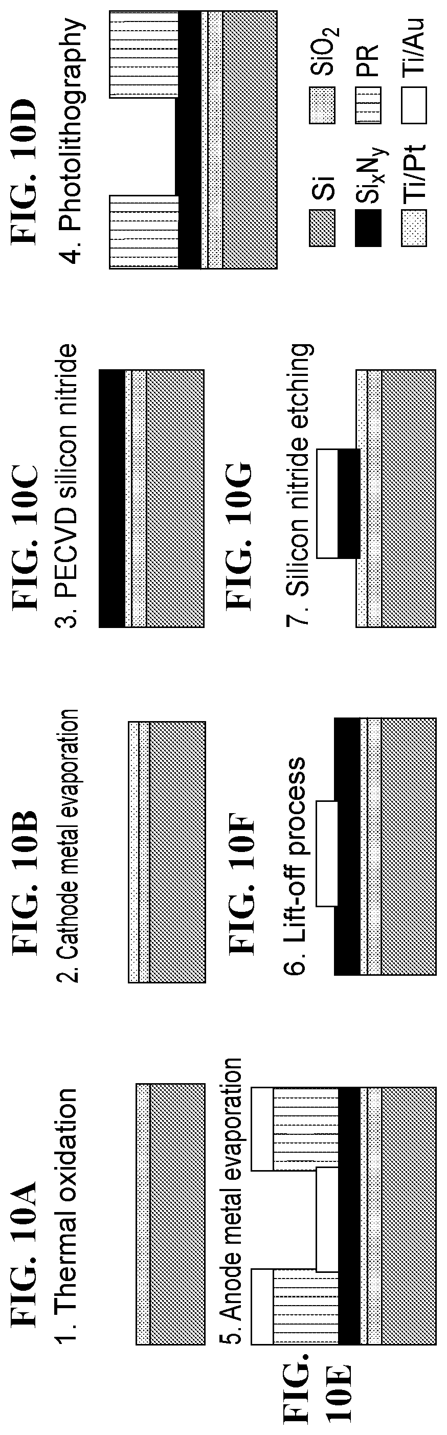
D00013

D00014
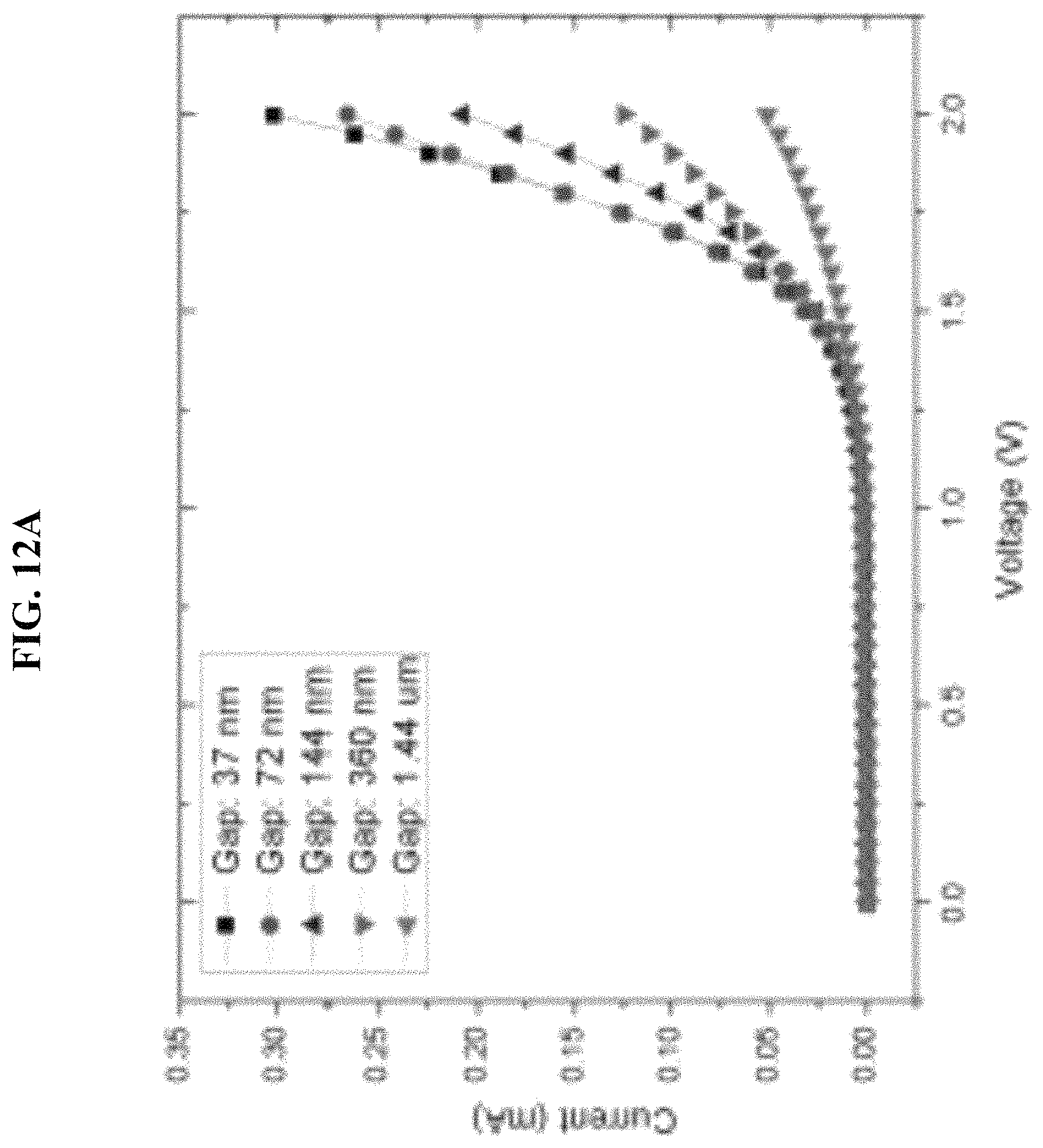
D00015
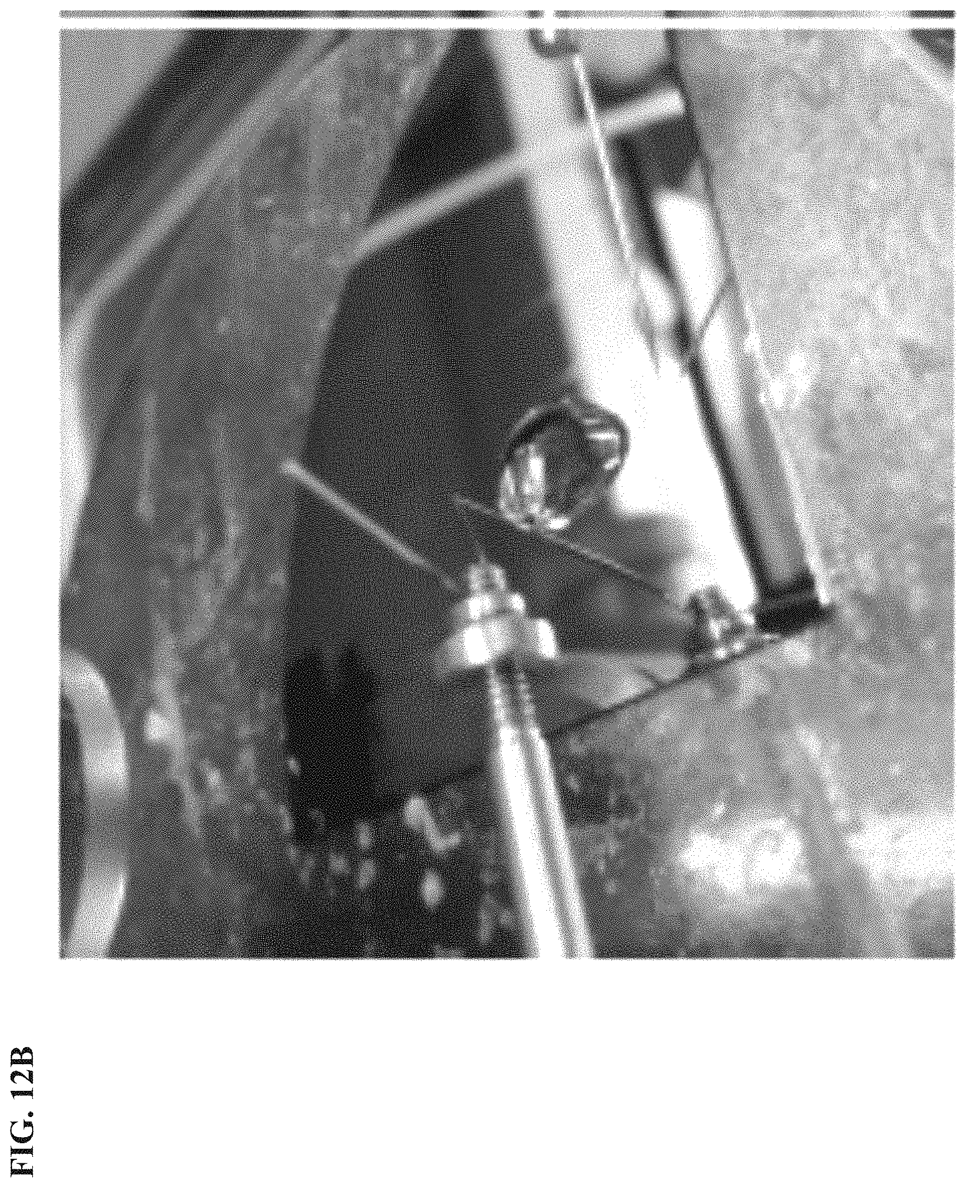
D00016
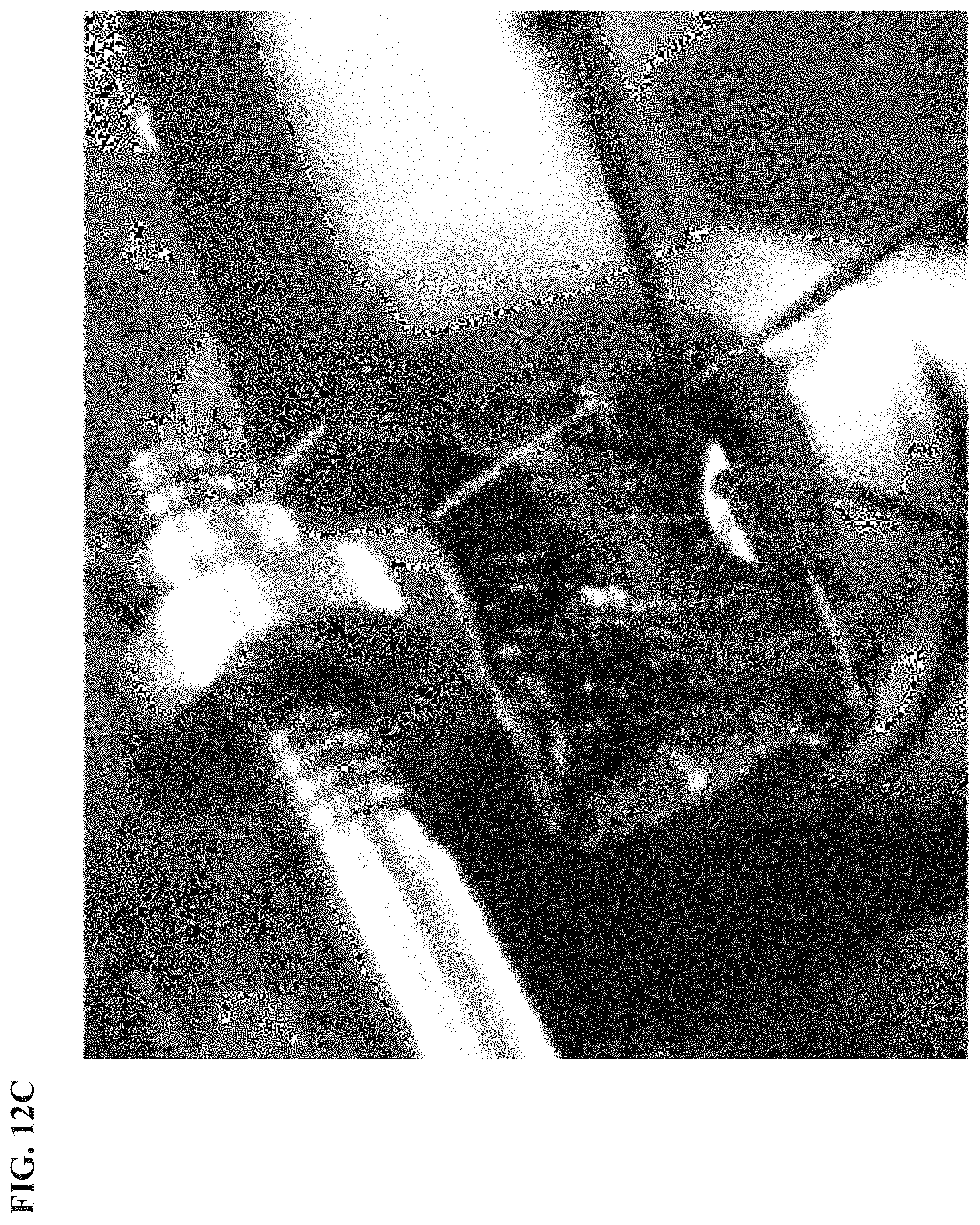
D00017
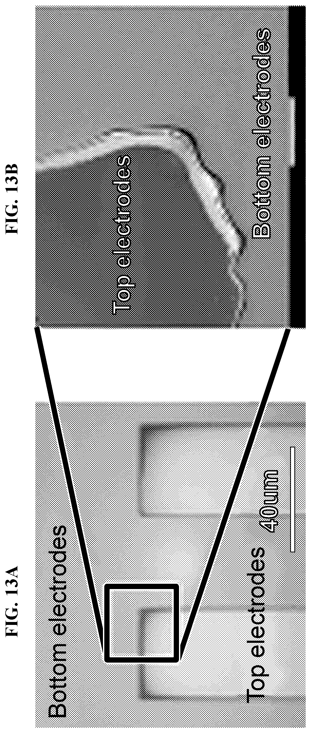
D00018

D00019

D00020
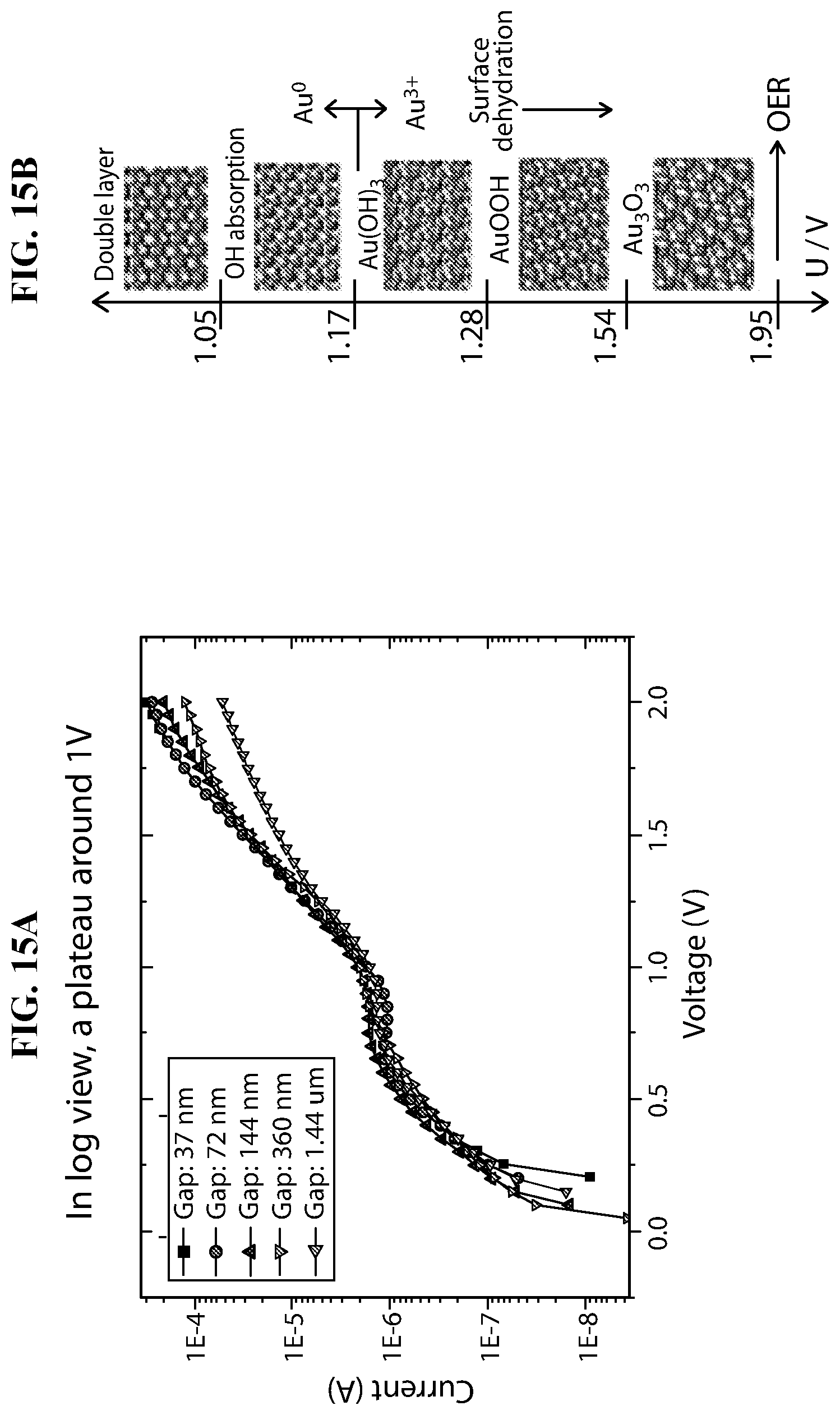
D00021

D00022

D00023

D00024
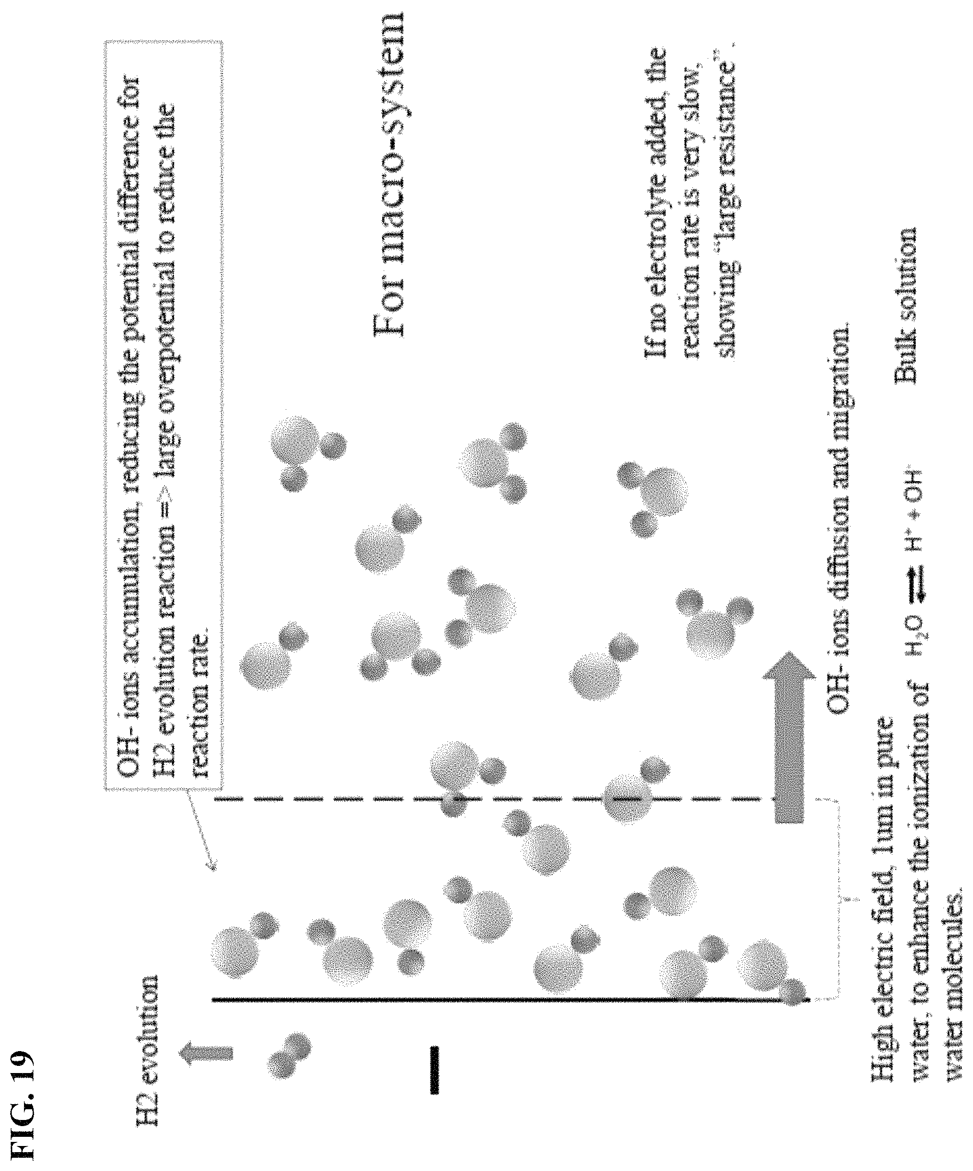
D00025

D00026
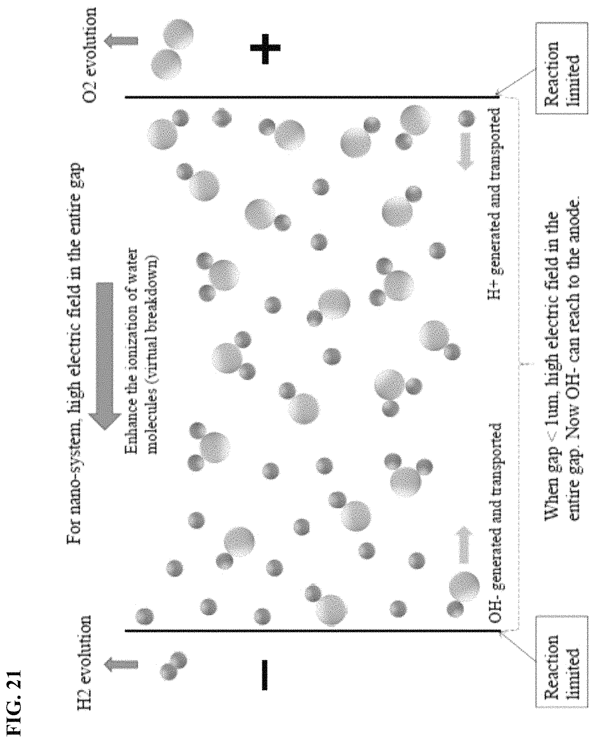
D00027
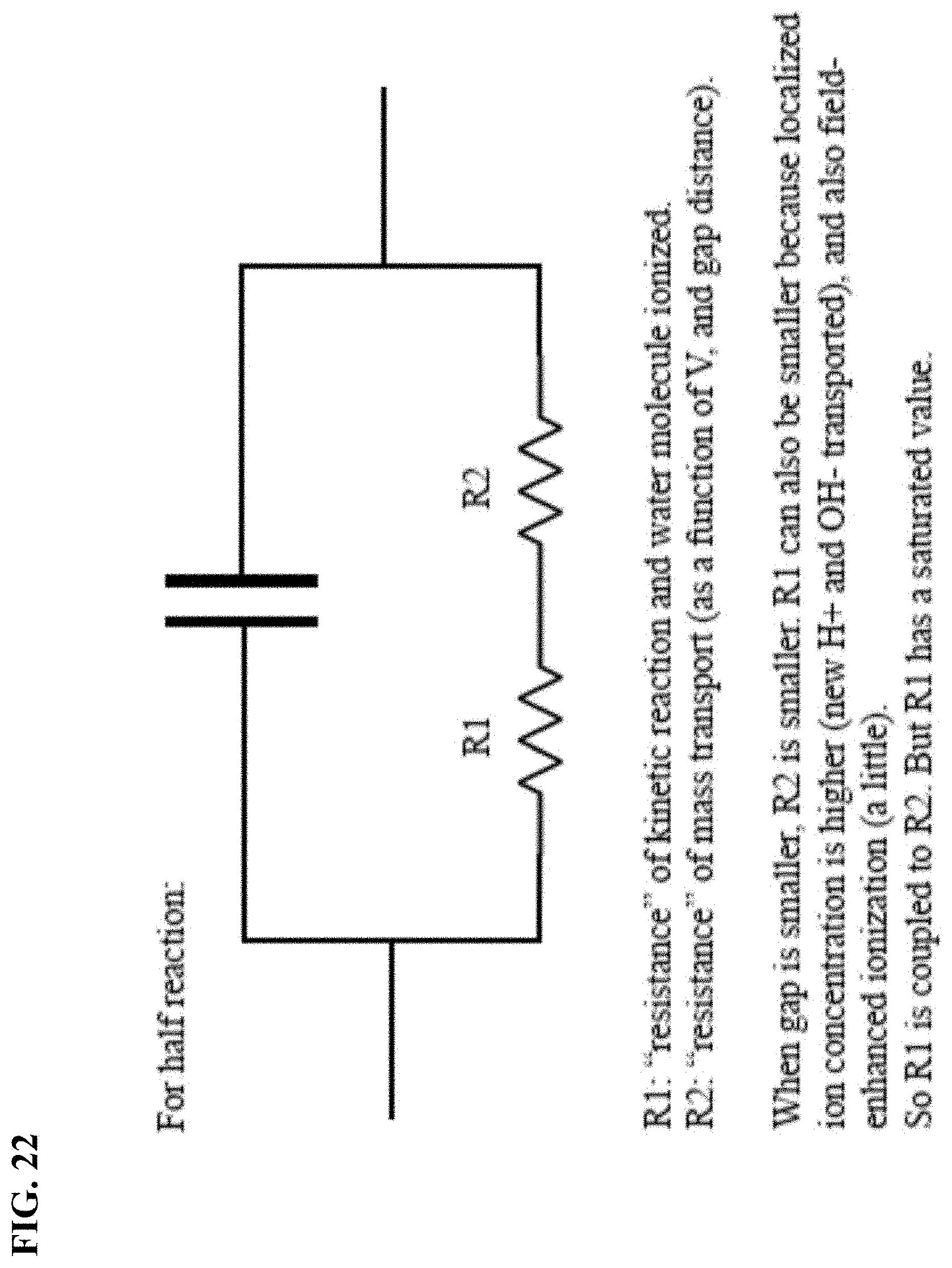
D00028

D00029

D00030
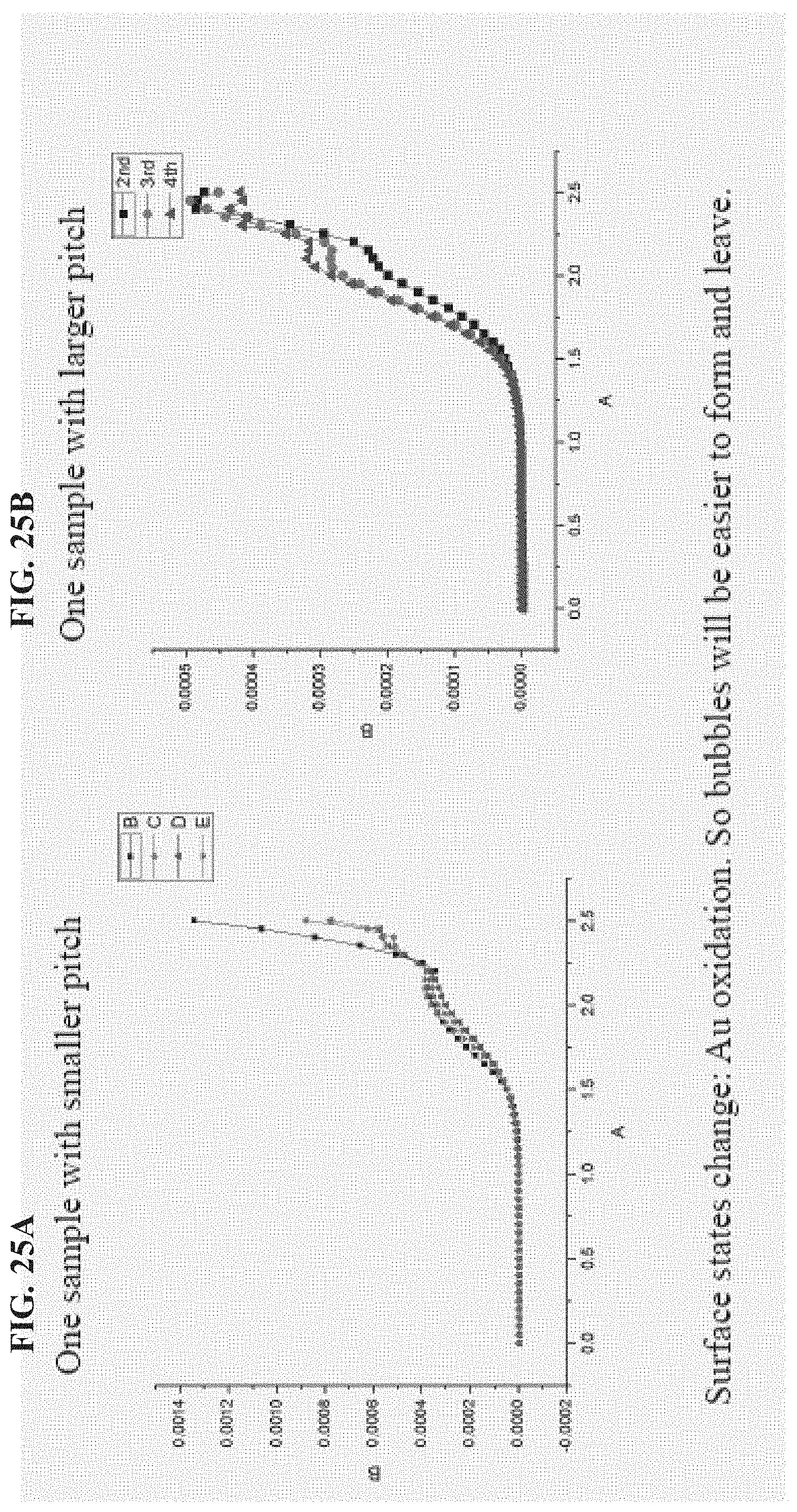
D00031

D00032

D00033

D00034
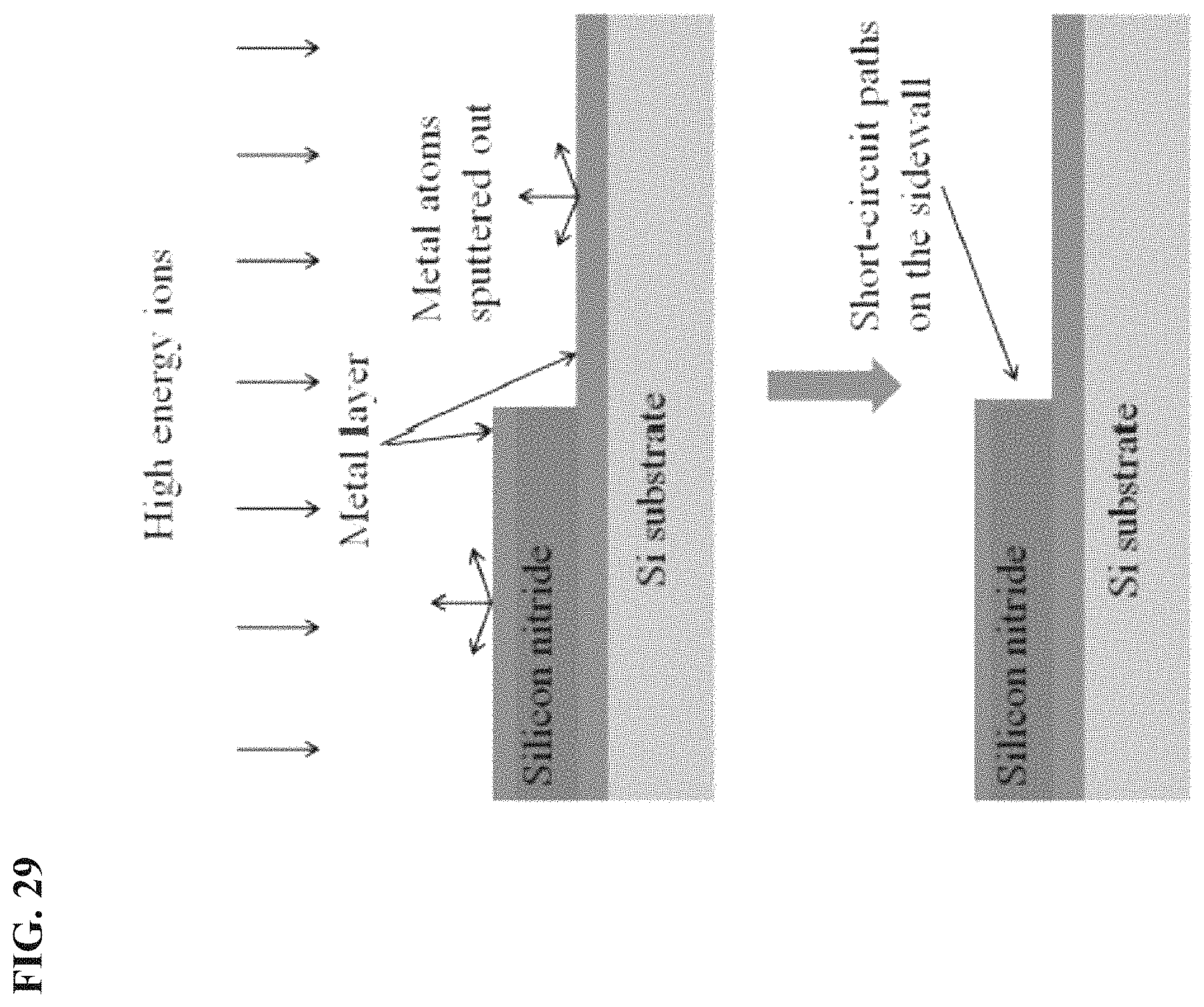
D00035

D00036
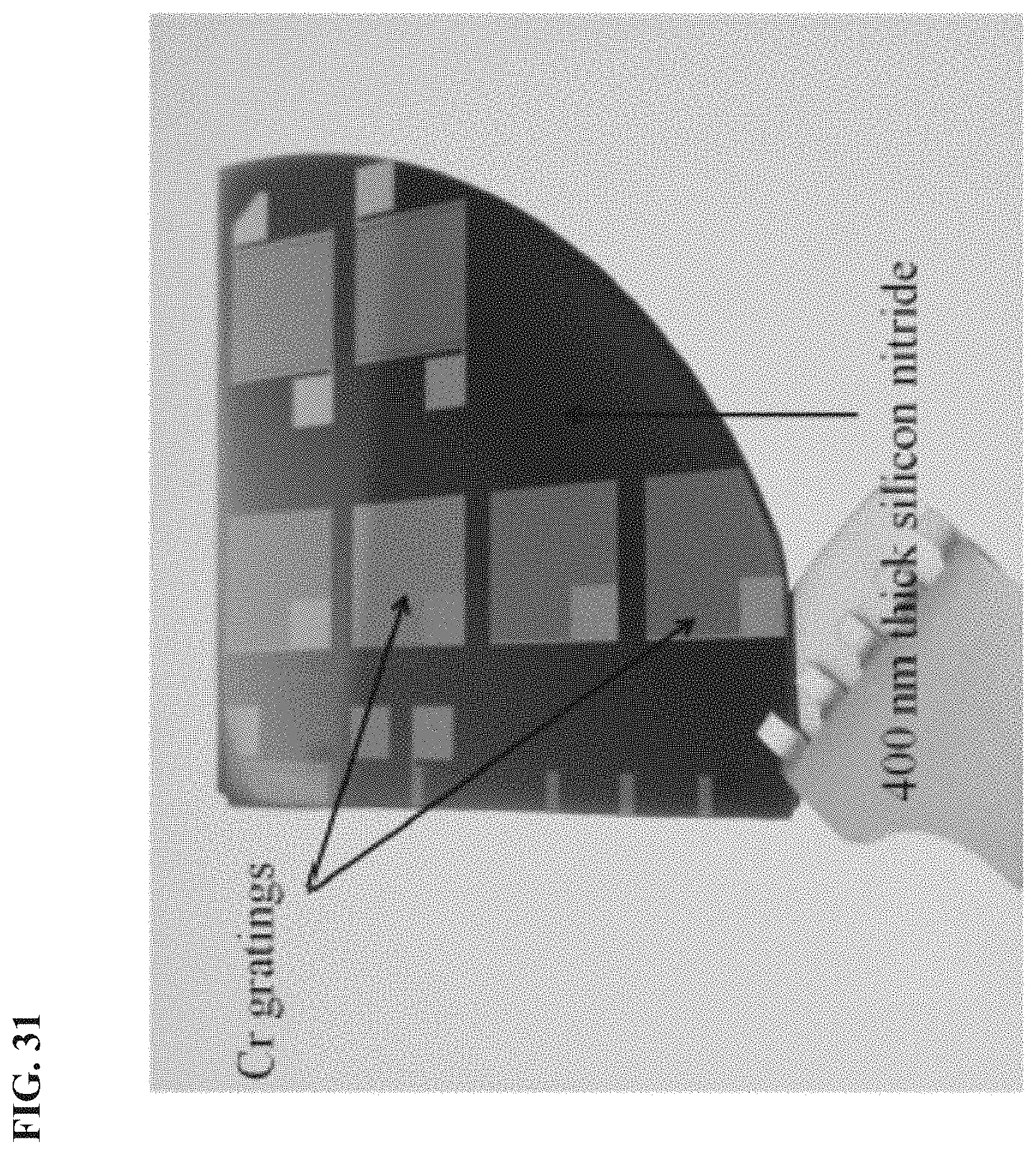
D00037
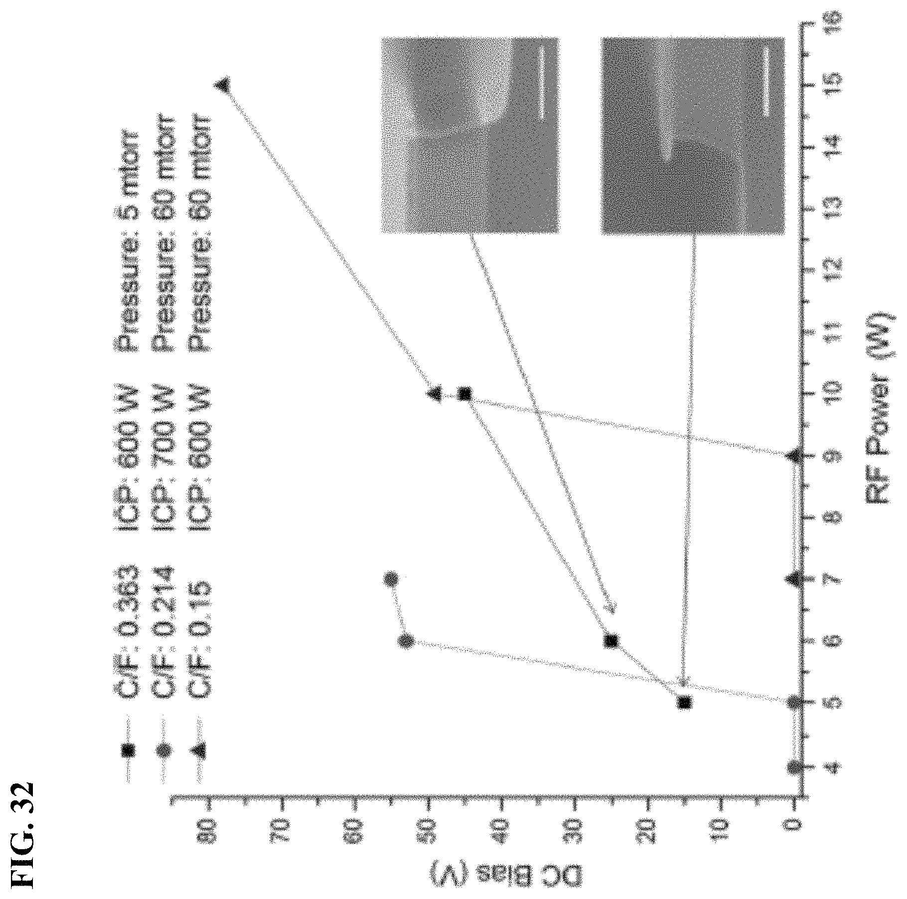
D00038
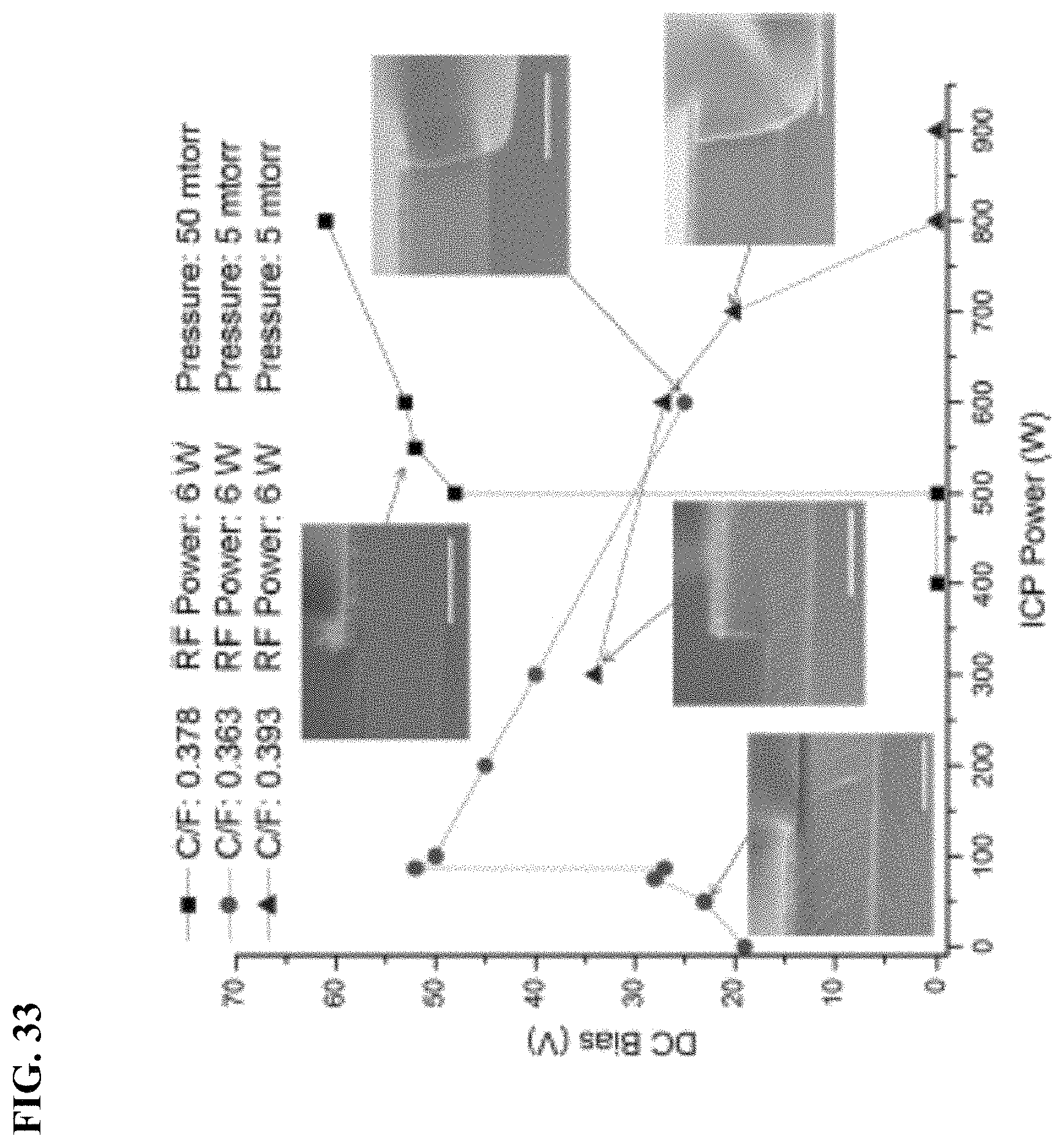
D00039

D00040

D00041

D00042

D00043

D00044

D00045
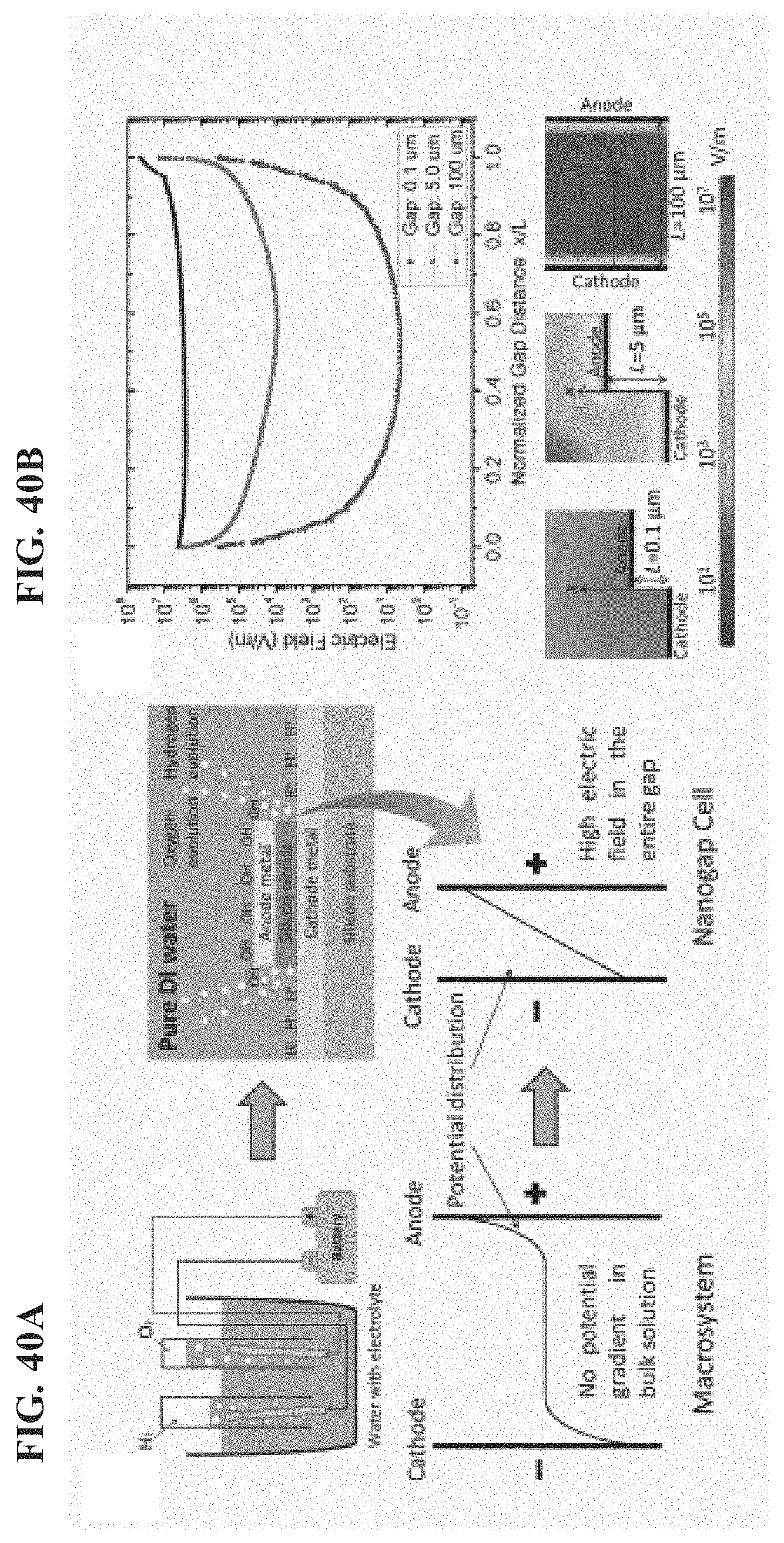
D00046

D00047

D00048

D00049
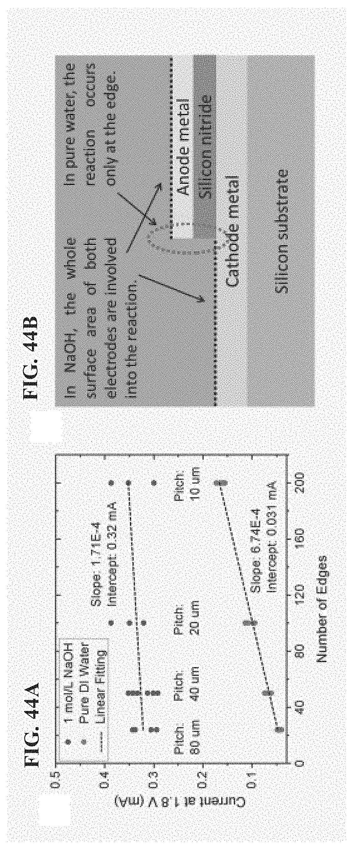
D00050

D00051
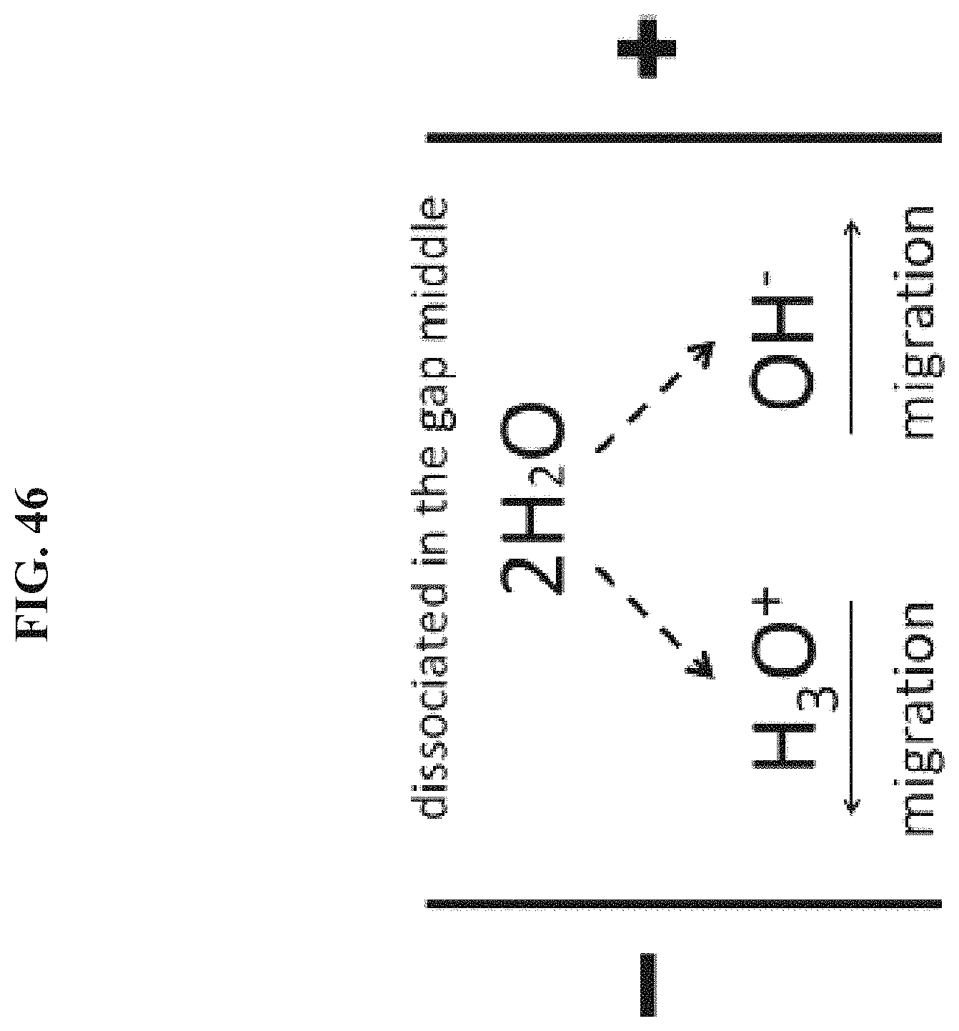
D00052

D00053
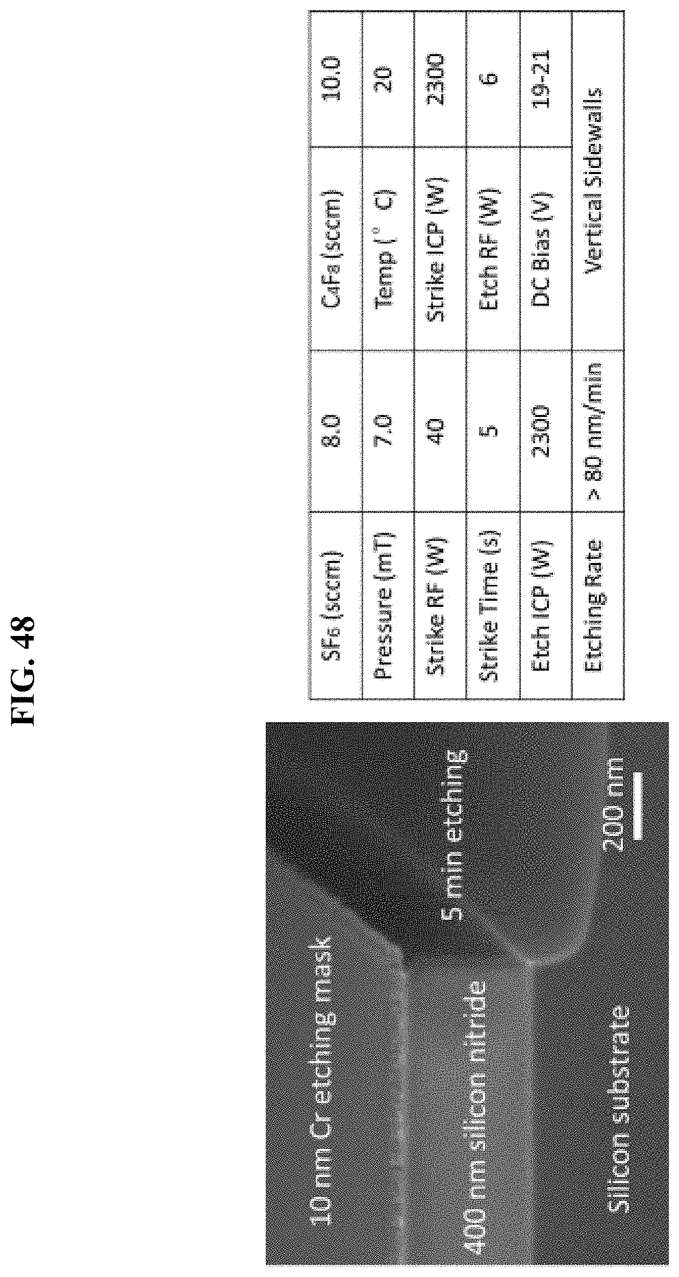
D00054
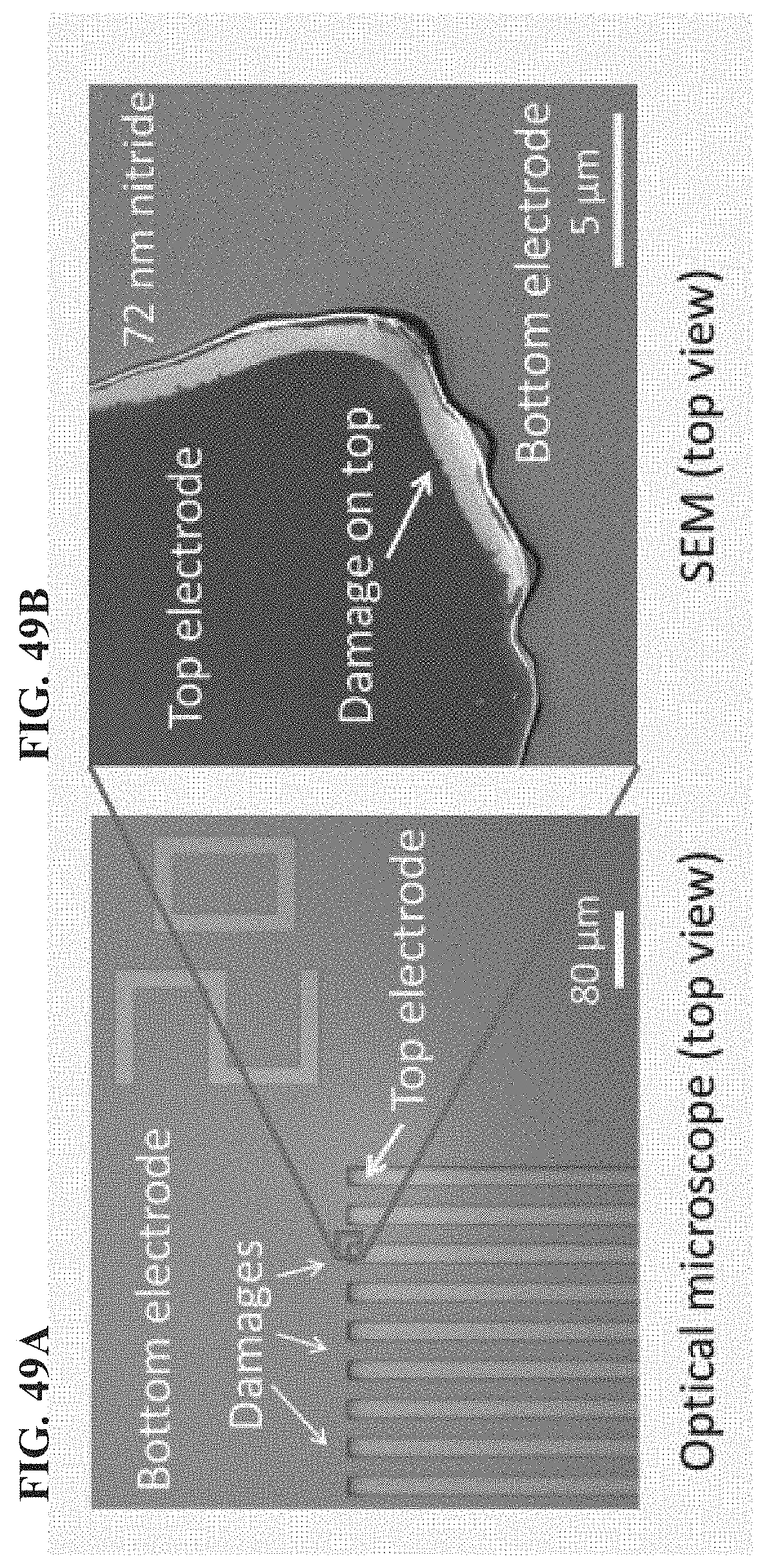
D00055

D00056

D00057

D00058

D00059

D00060
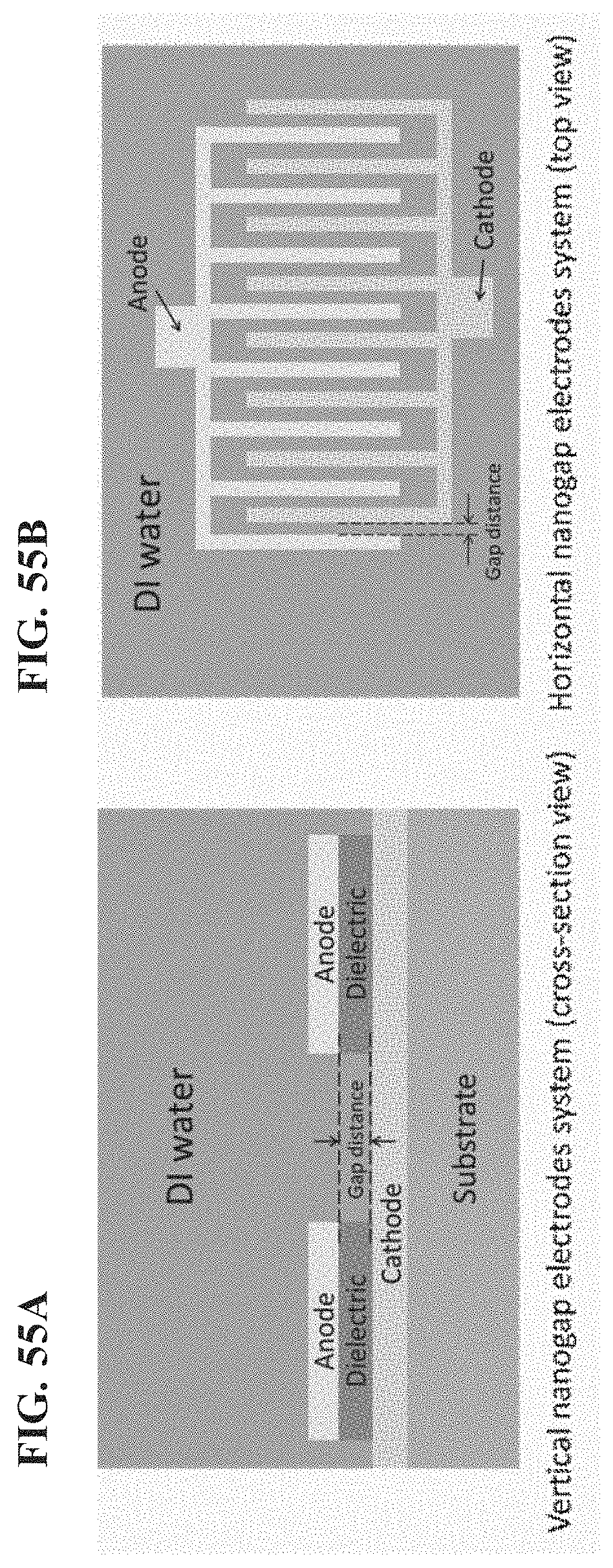
M00001

M00002

M00003

M00004

M00005

M00006

P00001

XML
uspto.report is an independent third-party trademark research tool that is not affiliated, endorsed, or sponsored by the United States Patent and Trademark Office (USPTO) or any other governmental organization. The information provided by uspto.report is based on publicly available data at the time of writing and is intended for informational purposes only.
While we strive to provide accurate and up-to-date information, we do not guarantee the accuracy, completeness, reliability, or suitability of the information displayed on this site. The use of this site is at your own risk. Any reliance you place on such information is therefore strictly at your own risk.
All official trademark data, including owner information, should be verified by visiting the official USPTO website at www.uspto.gov. This site is not intended to replace professional legal advice and should not be used as a substitute for consulting with a legal professional who is knowledgeable about trademark law.