Apparatus, systems and methods for generating voltage excitation waveforms
McFarland , et al.
U.S. patent number 10,613,559 [Application Number 16/295,231] was granted by the patent office on 2020-04-07 for apparatus, systems and methods for generating voltage excitation waveforms. This patent grant is currently assigned to RADIO SYSTEMS CORPORATION. The grantee listed for this patent is Radio Systems Corporation. Invention is credited to Keith R. Griffith, Scott A McFarland.


View All Diagrams
| United States Patent | 10,613,559 |
| McFarland , et al. | April 7, 2020 |
Apparatus, systems and methods for generating voltage excitation waveforms
Abstract
A method described herein includes describing a load current with a discrete time function. The method includes using a first frequency and a second frequency to provide an approximation of the described load current, wherein a transform applied to the discrete time function identifies the first frequency and the second frequency. The method includes estimating a loop inductance and a loop resistance of a wire loop by exciting a transmit circuit with a voltage reference step waveform, wherein the transmit circuit includes the wire loop. The method includes scaling the approximated load current to a level sufficient to generate a minimum receive voltage signal in a receiver at a first distance between the wire loop and the receiver. The method includes generating a first voltage signal using the scaled load current, estimated loop inductance, and estimated loop resistance. The method includes exciting the transmit circuit with the first voltage signal.
| Inventors: | McFarland; Scott A (Knoxville, TN), Griffith; Keith R. (Knoxville, TN) | ||||||||||
|---|---|---|---|---|---|---|---|---|---|---|---|
| Applicant: |
|
||||||||||
| Assignee: | RADIO SYSTEMS CORPORATION
(Knoxville, TN) |
||||||||||
| Family ID: | 59501144 | ||||||||||
| Appl. No.: | 16/295,231 | ||||||||||
| Filed: | March 7, 2019 |
Prior Publication Data
| Document Identifier | Publication Date | |
|---|---|---|
| US 20190204860 A1 | Jul 4, 2019 | |
Related U.S. Patent Documents
| Application Number | Filing Date | Patent Number | Issue Date | ||
|---|---|---|---|---|---|
| 15210498 | Jul 14, 2016 | 10268220 | |||
| Current U.S. Class: | 1/1 |
| Current CPC Class: | G05F 1/468 (20130101); H04B 1/04 (20130101); A01K 15/023 (20130101); G01R 19/02 (20130101) |
| Current International Class: | G05F 1/46 (20060101); G01R 19/02 (20060101); H04B 1/04 (20060101); A01K 15/02 (20060101) |
| Field of Search: | ;327/306-333 |
References Cited [Referenced By]
U.S. Patent Documents
| 2741224 | April 1956 | Putnam |
| 3182211 | May 1965 | Maratuech et al. |
| 3184730 | May 1965 | Irish |
| 3500373 | March 1970 | Arthur |
| 3735757 | May 1973 | MacFarland |
| 4426884 | January 1984 | Polchaninoff |
| 4783646 | November 1988 | Matsuzaki |
| 4794402 | December 1988 | Gonda et al. |
| 4802482 | February 1989 | Gonda et al. |
| 4947795 | August 1990 | Farkas |
| 4969418 | November 1990 | Jones |
| 5054428 | October 1991 | Farkus |
| 5159580 | October 1992 | Andersen et al. |
| 5161485 | November 1992 | McDade |
| 5182032 | January 1993 | Dickie et al. |
| 5207178 | May 1993 | McDade et al. |
| 5207179 | May 1993 | Arthur et al. |
| 5526006 | June 1996 | Akahane et al. |
| 5559498 | September 1996 | Westrick et al. |
| 5576972 | November 1996 | Harrison |
| 5586521 | December 1996 | Kelley |
| 5601054 | February 1997 | So |
| 5642690 | July 1997 | Calabrese et al. |
| 5794569 | August 1998 | Titus et al. |
| 5815077 | September 1998 | Christiansen |
| 5844489 | December 1998 | Yarnall, Jr. et al. |
| 5857433 | January 1999 | Files |
| 5870029 | February 1999 | Otto et al. |
| 5872516 | February 1999 | Bonge, Jr. |
| 5886669 | March 1999 | Kita |
| 5923254 | July 1999 | Brune |
| 5927233 | July 1999 | Mainini et al. |
| 5933079 | August 1999 | Frink |
| 5934225 | August 1999 | Williams |
| 5949350 | September 1999 | Girard et al. |
| 5957983 | September 1999 | Tominaga |
| 5982291 | November 1999 | Williams et al. |
| 6016100 | January 2000 | Boyd et al. |
| 6019066 | February 2000 | Taylor |
| 6028531 | February 2000 | Wanderlich |
| 6047664 | April 2000 | Lyerly |
| 6067018 | May 2000 | Skelton et al. |
| 6075443 | June 2000 | Schepps et al. |
| 6166643 | December 2000 | Janning et al. |
| 6170439 | January 2001 | Duncan et al. |
| 6184790 | February 2001 | Gerig |
| 6196990 | March 2001 | Zicherman |
| 6204762 | March 2001 | Dering et al. |
| 6215314 | April 2001 | Frankewich, Jr. |
| 6230031 | May 2001 | Barber |
| 6230661 | May 2001 | Yarnall, Jr. et al. |
| 6232880 | May 2001 | Anderson et al. |
| 6271757 | August 2001 | Touchton et al. |
| 6327999 | December 2001 | Gerig |
| 6353390 | March 2002 | Beri et al. |
| 6360697 | March 2002 | Williams |
| 6360698 | March 2002 | Stapelfeld et al. |
| 6404338 | June 2002 | Koslar |
| 6415742 | July 2002 | Lee et al. |
| 6426464 | July 2002 | Spellman et al. |
| 6427079 | July 2002 | Schneider et al. |
| 6431121 | August 2002 | Mainini et al. |
| 6431122 | August 2002 | Westrick et al. |
| 6441778 | August 2002 | Durst et al. |
| 6459378 | October 2002 | Gerig |
| 6487992 | December 2002 | Hollis |
| 6561137 | May 2003 | Oakman |
| 6581546 | June 2003 | Dalland et al. |
| 6588376 | July 2003 | Groh |
| 6598563 | July 2003 | Kim et al. |
| 6600422 | July 2003 | Barry et al. |
| 6637376 | October 2003 | Lee et al. |
| 6657544 | December 2003 | Barry et al. |
| 6668760 | December 2003 | Groh et al. |
| 6700492 | March 2004 | Touchton et al. |
| 6747555 | June 2004 | Fellenstein et al. |
| 6799537 | October 2004 | Liao |
| 6807720 | October 2004 | Brune et al. |
| 6820025 | November 2004 | Bachmann et al. |
| 6825768 | November 2004 | Stapelfeld et al. |
| 6830012 | December 2004 | Swan |
| 6833790 | December 2004 | Mejia et al. |
| 6874447 | April 2005 | Kobett |
| 6888502 | May 2005 | Beigel et al. |
| 6901883 | June 2005 | Gillis et al. |
| 6903682 | June 2005 | Maddox |
| 6907844 | June 2005 | Crist et al. |
| 6907883 | June 2005 | Lin |
| 6921089 | July 2005 | Groh et al. |
| 6923146 | August 2005 | Korbitz et al. |
| 6928958 | August 2005 | Crist et al. |
| 6937647 | August 2005 | Boyd et al. |
| 6956483 | October 2005 | Schmitt et al. |
| 6970090 | November 2005 | Sciarra |
| 7061385 | June 2006 | Fong et al. |
| 7079024 | July 2006 | Alarcon et al. |
| 7114466 | October 2006 | Mayer |
| 7142167 | November 2006 | Rochelle et al. |
| 7164354 | January 2007 | Panzer |
| 7173535 | February 2007 | Bach et al. |
| 7198009 | April 2007 | Crist et al. |
| 7222589 | May 2007 | Lee, IV et al. |
| 7249572 | July 2007 | Goetzl et al. |
| 7252051 | August 2007 | Napolez et al. |
| 7259718 | August 2007 | Patterson et al. |
| 7267081 | September 2007 | Steinbacher |
| 7275502 | October 2007 | Boyd et al. |
| 7296540 | November 2007 | Boyd |
| 7319397 | January 2008 | Chung et al. |
| 7328671 | February 2008 | Kates |
| 7339474 | March 2008 | Easley et al. |
| 7382328 | June 2008 | Lee, IV et al. |
| 7394390 | July 2008 | Gerig |
| 7395966 | July 2008 | Braiman |
| 7404379 | July 2008 | Nottingham et al. |
| 7411492 | August 2008 | Greenberg et al. |
| 7426906 | September 2008 | Nottingham et al. |
| 7434541 | October 2008 | Kates |
| 7443298 | October 2008 | Cole et al. |
| 7477155 | January 2009 | Bach et al. |
| 7503285 | March 2009 | Mainini et al. |
| 7518275 | April 2009 | Suzuki et al. |
| 7518522 | April 2009 | So et al. |
| 7538679 | May 2009 | Shanks |
| 7546817 | June 2009 | Moore |
| 7552699 | June 2009 | Moore |
| 7562640 | July 2009 | Lalor |
| 7565885 | July 2009 | Moore |
| 7574979 | August 2009 | Nottingham et al. |
| 7583931 | September 2009 | Eu et al. |
| 7602302 | October 2009 | Hokuf et al. |
| 7612668 | November 2009 | Harvey |
| 7616124 | November 2009 | Paessel et al. |
| 7656291 | February 2010 | Rochelle et al. |
| 7667599 | February 2010 | Mainini et al. |
| 7667607 | February 2010 | Gerig et al. |
| 7680645 | March 2010 | Li et al. |
| 7705736 | April 2010 | Kedziora |
| 7710263 | May 2010 | Boyd |
| 7760137 | July 2010 | Martucci et al. |
| 7779788 | August 2010 | Moore |
| 7786876 | August 2010 | Troxler et al. |
| 7804724 | September 2010 | Way |
| 7814865 | October 2010 | Tracy et al. |
| 7828221 | November 2010 | Kwon |
| 7830257 | November 2010 | Hassell |
| 7834769 | November 2010 | Hinkle et al. |
| 7841301 | November 2010 | Mainini et al. |
| 7856947 | December 2010 | Giunta |
| 7864057 | January 2011 | Milnes et al. |
| 7868912 | January 2011 | Venetianer et al. |
| 7900585 | March 2011 | Lee et al. |
| 7918190 | April 2011 | Belcher et al. |
| 7944359 | May 2011 | Fong et al. |
| 7946252 | May 2011 | Lee, IV et al. |
| 7978078 | July 2011 | Copeland et al. |
| 7996983 | August 2011 | Lee et al. |
| 8011327 | September 2011 | Mainini et al. |
| 8047161 | November 2011 | Moore et al. |
| 8049630 | November 2011 | Chao et al. |
| 8065978 | November 2011 | Duncan et al. |
| 8069823 | December 2011 | Mainini et al. |
| 8098164 | January 2012 | Gerig et al. |
| 8159355 | April 2012 | Gerig et al. |
| 8185345 | May 2012 | Mainini |
| 8232909 | July 2012 | Kroeger et al. |
| 8240085 | August 2012 | Hill |
| 8269504 | September 2012 | Gerig |
| 8274396 | September 2012 | Gurley et al. |
| 8297233 | October 2012 | Rich et al. |
| 8342134 | January 2013 | Lee et al. |
| 8342135 | January 2013 | Peinetti et al. |
| 8430064 | April 2013 | Groh et al. |
| 8436735 | May 2013 | Mainini et al. |
| 8447510 | May 2013 | Fitzpatrick et al. |
| 8451130 | May 2013 | Mainini |
| 8456296 | June 2013 | Piltonen et al. |
| 8483262 | July 2013 | Mainini et al. |
| 8714113 | May 2014 | Lee, IV et al. |
| 8715824 | May 2014 | Rawlings et al. |
| 8736499 | May 2014 | Goetzl et al. |
| 8779925 | July 2014 | Rich et al. |
| 8803692 | August 2014 | Goetzl et al. |
| 8807089 | August 2014 | Brown et al. |
| 8823513 | September 2014 | Jameson et al. |
| 8854215 | October 2014 | Ellis et al. |
| 8866605 | October 2014 | Gibson |
| 8908034 | December 2014 | Bordonaro |
| 8917172 | December 2014 | Charych |
| 8947240 | February 2015 | Mainini |
| 8967085 | March 2015 | Gillis et al. |
| 9035773 | May 2015 | Petersen et al. |
| 9125380 | September 2015 | Deutsch |
| 9131660 | September 2015 | Womble |
| 9186091 | November 2015 | Mainini et al. |
| 9204251 | December 2015 | Mendelson et al. |
| 9307745 | April 2016 | Mainini |
| 9861076 | January 2018 | Rochelle et al. |
| 2002/0010390 | January 2002 | Guice et al. |
| 2002/0015094 | February 2002 | Kuwano et al. |
| 2002/0036569 | March 2002 | Martin |
| 2002/0092481 | July 2002 | Spooner |
| 2002/0103610 | August 2002 | Bachmann et al. |
| 2002/0196151 | December 2002 | Troxler |
| 2003/0034887 | February 2003 | Crabtree et al. |
| 2003/0035051 | February 2003 | Cho et al. |
| 2003/0116099 | June 2003 | Kim et al. |
| 2003/0169207 | September 2003 | Beigel et al. |
| 2003/0179140 | September 2003 | Patterson et al. |
| 2003/0218539 | November 2003 | Hight |
| 2004/0108939 | June 2004 | Giunta |
| 2004/0162875 | August 2004 | Brown |
| 2005/0000469 | January 2005 | Giunta et al. |
| 2005/0007251 | January 2005 | Crabtree et al. |
| 2005/0020279 | January 2005 | Markhovsky et al. |
| 2005/0035865 | February 2005 | Brennan et al. |
| 2005/0059909 | March 2005 | Burgess |
| 2005/0066912 | March 2005 | Korbitz et al. |
| 2005/0081797 | April 2005 | Laitinen et al. |
| 2005/0139169 | June 2005 | So et al. |
| 2005/0145196 | July 2005 | Crist et al. |
| 2005/0145198 | July 2005 | Crist et al. |
| 2005/0145200 | July 2005 | Napolez et al. |
| 2005/0172912 | August 2005 | Crist et al. |
| 2005/0217606 | October 2005 | Lee et al. |
| 2005/0231353 | October 2005 | Dipoala et al. |
| 2005/0235924 | October 2005 | Lee, IV et al. |
| 2005/0258715 | November 2005 | Schlabach et al. |
| 2005/0263106 | December 2005 | Steinbacher |
| 2005/0280546 | December 2005 | Ganley |
| 2005/0288007 | December 2005 | Benco et al. |
| 2006/0000015 | January 2006 | Duncan |
| 2006/0011145 | January 2006 | Kates et al. |
| 2006/0027185 | February 2006 | Troxler et al. |
| 2006/0092676 | May 2006 | Liptak et al. |
| 2006/0102101 | May 2006 | Kim |
| 2006/0112901 | June 2006 | Gomez |
| 2006/0191491 | August 2006 | Nottingham et al. |
| 2006/0196445 | September 2006 | Kates |
| 2006/0197672 | September 2006 | Talamas, Jr. et al. |
| 2006/0202818 | September 2006 | Greenberg et al. |
| 2007/0011339 | January 2007 | Brown |
| 2007/0103296 | May 2007 | Paessel et al. |
| 2007/0204803 | September 2007 | Ramsay |
| 2007/0204804 | September 2007 | Swanson et al. |
| 2007/0249470 | October 2007 | Niva et al. |
| 2007/0266959 | November 2007 | Brooks et al. |
| 2008/0004539 | January 2008 | Ross |
| 2008/0017133 | January 2008 | Moore |
| 2008/0036610 | February 2008 | Hokuf et al. |
| 2008/0055154 | March 2008 | Martucci et al. |
| 2008/0055155 | March 2008 | Hensley et al. |
| 2008/0058670 | March 2008 | Mainini et al. |
| 2008/0061978 | March 2008 | Huang |
| 2008/0061990 | March 2008 | Milnes et al. |
| 2008/0119757 | May 2008 | Winter |
| 2008/0129457 | June 2008 | Ritter et al. |
| 2008/0141949 | June 2008 | Taylor |
| 2008/0143516 | June 2008 | Mock et al. |
| 2008/0156277 | July 2008 | Mainini et al. |
| 2008/0163827 | July 2008 | Goetzl |
| 2008/0163829 | July 2008 | Lee et al. |
| 2008/0168949 | July 2008 | Belcher et al. |
| 2008/0168950 | July 2008 | Moore et al. |
| 2008/0186167 | August 2008 | Ramachandra |
| 2008/0186197 | August 2008 | Rochelle et al. |
| 2008/0204322 | August 2008 | Oswald et al. |
| 2008/0236514 | October 2008 | Johnson et al. |
| 2008/0252527 | October 2008 | Garcia |
| 2008/0272908 | November 2008 | Boyd |
| 2009/0000566 | January 2009 | Kim |
| 2009/0002188 | January 2009 | Greenberg |
| 2009/0012355 | January 2009 | Lin |
| 2009/0020002 | January 2009 | Williams et al. |
| 2009/0025651 | January 2009 | Lalor |
| 2009/0031966 | February 2009 | Kates |
| 2009/0082830 | March 2009 | Folkerts et al. |
| 2009/0102668 | April 2009 | Thompson et al. |
| 2009/0224909 | September 2009 | Derrick et al. |
| 2009/0239586 | September 2009 | Boeve et al. |
| 2009/0289785 | November 2009 | Leonard |
| 2009/0289844 | November 2009 | Palsgrove et al. |
| 2010/0008011 | January 2010 | Ogram |
| 2010/0033339 | February 2010 | Gurley et al. |
| 2010/0047119 | February 2010 | Cressy |
| 2010/0049364 | February 2010 | Landry et al. |
| 2010/0107985 | May 2010 | O'Hare |
| 2010/0139576 | June 2010 | Kim et al. |
| 2010/0154721 | June 2010 | Gerig et al. |
| 2010/0231391 | September 2010 | Dror et al. |
| 2010/0238022 | September 2010 | Au et al. |
| 2010/0315241 | December 2010 | Jow |
| 2011/0140967 | June 2011 | Lopez et al. |
| 2012/0000431 | January 2012 | Khoshkish et al. |
| 2012/0006282 | January 2012 | Kates |
| 2012/0037088 | February 2012 | Altenhofen |
| 2012/0078139 | March 2012 | Aldridge |
| 2012/0132151 | May 2012 | Touchton et al. |
| 2012/0165012 | June 2012 | Fischer et al. |
| 2012/0188370 | July 2012 | Bordonaro |
| 2012/0236688 | September 2012 | Spencer et al. |
| 2012/0312250 | December 2012 | Jesurum |
| 2013/0099920 | April 2013 | Song et al. |
| 2013/0099922 | April 2013 | Lohbihler |
| 2013/0141237 | June 2013 | Goetzl et al. |
| 2013/0157564 | June 2013 | Curtis et al. |
| 2013/0169441 | July 2013 | Wilson |
| 2013/0321159 | December 2013 | Schofield et al. |
| 2014/0020635 | January 2014 | Sayers et al. |
| 2014/0053788 | February 2014 | Riddell |
| 2014/0062695 | March 2014 | Rosen et al. |
| 2014/0069350 | March 2014 | Riddell |
| 2014/0073939 | March 2014 | Rodriguez-Llorente et al. |
| 2014/0120943 | May 2014 | Shima |
| 2014/0123912 | May 2014 | Menkes et al. |
| 2014/0132608 | May 2014 | Mund et al. |
| 2014/0174376 | June 2014 | Touchton et al. |
| 2014/0228649 | August 2014 | Rayner et al. |
| 2014/0253389 | September 2014 | Beauregard |
| 2014/0261235 | September 2014 | Rich et al. |
| 2014/0267299 | September 2014 | Couse |
| 2014/0275824 | September 2014 | Couse et al. |
| 2014/0320347 | October 2014 | Rochelle et al. |
| 2015/0040840 | February 2015 | Muetzel et al. |
| 2015/0053144 | February 2015 | Bianchi et al. |
| 2015/0075446 | March 2015 | Hu |
| 2015/0080013 | March 2015 | Venkatraman et al. |
| 2015/0107531 | April 2015 | Golden |
| 2015/0149111 | May 2015 | Kelly et al. |
| 2015/0163412 | June 2015 | Holley et al. |
| 2015/0172872 | June 2015 | Alsehly et al. |
| 2015/0173327 | June 2015 | Gerig et al. |
| 2015/0199490 | July 2015 | Iancu et al. |
| 2015/0223013 | August 2015 | Park et al. |
| 2015/0289111 | October 2015 | Ozkan et al. |
| 2015/0350848 | December 2015 | Eramian |
| 2016/0015005 | January 2016 | Brown, Jr. et al. |
| 2016/0021506 | January 2016 | Bonge, Jr. |
| 2016/0021850 | January 2016 | Stapelfeld et al. |
| 2016/0044444 | February 2016 | Rattner et al. |
| 2016/0094419 | March 2016 | Peacock et al. |
| 2016/0102879 | April 2016 | Guest et al. |
| 2016/0150362 | May 2016 | Shaprio et al. |
| 2016/0174099 | June 2016 | Goldfain |
| 2016/0178392 | June 2016 | Goldfain |
| 2016/0187454 | June 2016 | Orman et al. |
| 2016/0253987 | September 2016 | Chattell |
| 2016/0363664 | December 2016 | Mindell et al. |
| 2017/0323630 | November 2017 | Stickney et al. |
| 2018/0027772 | February 2018 | Gordon et al. |
| 2018/0094451 | April 2018 | Peter et al. |
| 2018/0234134 | August 2018 | Tang et al. |
| 2018/0235182 | August 2018 | Bocknek |
| 2018/0315262 | November 2018 | Love et al. |
| 2019/0013003 | January 2019 | Baughman et al. |
| 2019/0165832 | May 2019 | Khanduri et al. |
| 101112181 | Jan 2008 | CN | |||
| 101937015 | Jan 2011 | CN | |||
| 101112181 | Nov 2012 | CN | |||
| 102793568 | Dec 2014 | CN | |||
| H0974774 | Mar 1997 | JP | |||
| 20130128704 | Nov 2013 | KR | |||
| WO-02060240 | Feb 2003 | WO | |||
| WO-2006000015 | Jan 2006 | WO | |||
| WO-2008085812 | Jul 2008 | WO | |||
| WO-2008140992 | Nov 2008 | WO | |||
| WO-2009105243 | Aug 2009 | WO | |||
| WO-2009106896 | Sep 2009 | WO | |||
| WO-2011055004 | May 2011 | WO | |||
| WO-2011136816 | Nov 2011 | WO | |||
| WO-2012122607 | Sep 2012 | WO | |||
| WO-2015015047 | Feb 2015 | WO | |||
| WO-2016204799 | Dec 2016 | WO | |||
Other References
|
Extended European Search Report for Application No. EP17180645, dated May 9, 2018, 7 pages. cited by applicant . Baba A.I., et al., "Calibrating Time of Flight in Two Way Ranging," IEEE Xplore Digital Library, Dec. 2011, pp. 393-397. cited by applicant . Extended European Search Report for European Application No. 11784149.4 dated Nov. 17, 2017, 7 pages. cited by applicant . Extended European Search Report for European Application No. 15735439.0 dated Oct. 18, 2017, 9 pages. cited by applicant . Extended European Search Report for European Application No. 15895839.7 dated Oct. 9, 2018, 5 pages. cited by applicant . Extended European Search Report for European Application No. 17162289.7 dated Aug. 31, 2017, 7 pages. cited by applicant . High Tech Products, Inc: "Human Contain Model X-10 Rechargeable Muti-function Electronic Dog Fence Ultra-system", Internet citation, Retrieved from the Internet: URL:http://web.archive.org/web/20120112221915/http://hightechpet.com/user- _Manuals/HC%20X-10_Press.pdf retrieved on Apr. 10, 2017], Apr. 28, 2012, pp. 1-32, XP008184171. cited by applicant . International Preliminary Report for Patentability Chapter II for International Application No. PCT/US2014/024875 dated Mar. 12, 2015, 17 pages. cited by applicant . International Preliminary Report on Patentability for Application No. PCT/US2015/043653 dated Dec. 19, 2017, 14 pages. cited by applicant . International Search Report and Written Opinion for Application No. PCT/US2018/013737 dated Mar. 7, 2018, 8 pages. cited by applicant . International Search Report and Written Opinion for Application No. PCT/US2018/013738 dated Mar. 20, 2018, 6 pages. cited by applicant . International Search Report and Written Opinion for Application No. PCT/US2018/013740 dated Mar. 20, 2018, 6 pages. cited by applicant . International Search Report and Written Opinion for Application No. PCT/US2018/019887 dated May 8, 2018, 10 pages. cited by applicant . International Search Report and Written Opinion for International Application No. PCT/US2014/024875 dated Jun. 27, 2014, 12 pages. cited by applicant . International Search Report for International Application No. PCT/US2014/020344 dated Jun. 5, 2014, 2 pages. cited by applicant . International Search Report for International Application No. PCT/US2014/066650 dated Feb. 19, 2015, 3 pages (Outgoing). cited by applicant . International Search Report for International Application No. PCT/US2015/010864, Form PCT/ISA/210 dated Apr. 13, 2015, 2 pages. cited by applicant . International Search Report for International Application No. PCT/US2015/043653, Form PCT/ISA/210 dated Oct. 23, 2015, 2 pages. cited by applicant . Notification of Transmittal of the International Search Report and the Written Opinion of the International Searching Authority for International Application No. PCT/US2015/043653, Form PCT/ISA/220 dated Oct. 23, 2015, 1 page. cited by applicant . Notification of Transmittal of the International Search Report and Written Opinion for the International Application No. PCT/US2014/066650 dated Feb. 19, 2015, 1 page. cited by applicant . Welch et al., "An Introduction to the Kalman Filter," Department of Computer Science, Jul. 24, 2006, pp. 1-16. cited by applicant . Written Opinion for International Application No. PCT/US2014/066650 dated Feb. 19, 2015, 15 pages(outgoing). cited by applicant . Written Opinion for International Application No. PCT/US2015/043653, Form PCT/ISA/237 dated Oct. 23, 2015, 13 pages. cited by applicant . Written Opinion of the International Application No. PCT/US2015/010864, Form PCT/ISA/237 dated Apr. 13, 2015, 6 pages. cited by applicant . Eileen--How to Protect Your Dog From Loud and Scary Sounds (Year: 2013). cited by applicant. |
Primary Examiner: Donovan; Lincoln D
Assistant Examiner: Cheng; Diana J.
Attorney, Agent or Firm: Baker, Donelson, Bearman, Caldwell & Berkowitz PC
Parent Case Text
CROSS REFERENCE TO RELATED APPLICATIONS
This application is a continuation application of U.S. application Ser. No. 15/210,498, filed Jul. 14, 2016.
Claims
We claim:
1. A method comprising, one or more applications running on at least one processor for providing, describing a load current with a discrete time function; using a first frequency and a second frequency to provide an approximation of the described load current, wherein a transform applied to the discrete time function identifies the first frequency and the second frequency; estimating a loop inductance and a loop resistance of a wire loop by exciting a transmit circuit with a voltage reference step waveform, wherein the transmit circuit includes the wire loop; scaling the approximated load current to a level sufficient to generate a minimum receive voltage signal in a receiver at a first distance between the wire loop and the receiver; generating a first voltage signal using the scaled load current, the estimated loop inductance, and the estimated loop resistance; exciting the transmit circuit with the first voltage signal; reading a voltage signal at a location in the transmit circuit, wherein the voltage signal is representative of a corresponding transmit current in the transmit circuit; and processing the voltage signal to estimate a receive voltage signal, the estimating including determining an asymmetry of the estimated receive voltage signal.
2. The method of claim 1, wherein the estimating the loop inductance and the loop resistance includes monitoring the transmit circuit's current in response to the voltage reference step waveform.
3. The method of claim 2, wherein the monitoring the transmit circuit's current includes capturing current amplitude as a function of time in response to the voltage reference step waveform.
4. The method of claim 1, wherein the transform comprises a Discrete Fourier Transform.
5. The method of claim 1, wherein the first frequency comprises a first harmonic frequency of the described load current.
6. The method of claim 5, wherein the second frequency comprises a second harmonic frequency of the described load current.
7. The method of claim 6, comprising generating a first carrier component of the approximated load current using the first harmonic frequency, wherein the first carrier component has a weight of one.
8. The method of claim 7, comprising generating a second carrier component of the approximated load current using the second harmonic frequency, wherein an amplitude of the second carrier component is weighted relative to an amplitude of the first carrier component.
9. The method of claim 8, wherein the transform applied to the discrete time function used to describe the load current identifies the relative weight of the second carrier component.
10. The method of claim 8, wherein the providing the approximation of the described load current includes summing the first carrier component and the second carrier component.
11. The method of claim 1, wherein the approximated load current comprises a discrete time function.
12. The method of claim 1, wherein the first voltage signal comprises a discrete time function.
13. The method of claim 1, wherein an input to the discrete time function used to describe the load current comprises a rotating phasor.
14. The method of claim 13, wherein the phasor value periodically rotates between 0 and 2.pi. radians.
15. The method of claim 14, wherein the discrete time function used to describe the load current has a first slope when the phasor value is within a first range.
16. The method of claim 15, wherein the first slope is positive.
17. The method of claim 15, wherein the discrete time function used to describe the load current has a second slope when the phasor value is within a second range.
18. The method of claim 15, wherein the second slope is negative.
19. The method of claim 15, wherein the first range comprises approximately thirty percent of 2.pi. radians.
20. The method of claim 19, wherein the absolute value of the first slope is greater than the absolute value of the second slope.
21. The method of claim 1, the estimating including determining a root mean square (RMS) of the estimated receive voltage signal.
22. The method of claim 21, wherein the asymmetry comprises a ratio of the aggregate positive and aggregate negative peaks of the estimated receive voltage signal.
23. The method of claim 21, comprising establishing a target RMS value.
24. The method of claim 23, wherein a target RMS range comprises the target RMS value plus or minus a percentage.
25. The method of claim 24, comprising establishing a target asymmetry value.
26. The method of claim 25, wherein a target asymmetry range comprises the target asymmetry value plus or minus a percentage.
27. The method of claim 26, comprising iteratively adjusting an impedance vector of the transmit circuit until the RMS and the asymmetry of the estimated receive voltage signal fall within the corresponding target RMS and asymmetry ranges, wherein the impedance vector initially comprises the loop resistance and the loop inductance.
28. The method of claim 27, the adjusting comprising scaling the impedance vector when the RMS falls outside the target RMS range.
29. The method of claim 27, the adjusting comprising rotating a phase angle of the impedance vector when the asymmetry falls outside the target asymmetry range.
30. The method of claim 29, the rotating the phase angle comprising a negative rotation.
31. The method of claim 29, the rotating the phase angle comprising a positive rotation.
32. The method of claim 1, wherein the described load current comprises an asymmetry.
33. The method of claim 32, wherein the receiver exploits the asymmetry to determine the receiver's direction of approach to the wire loop carrying the described load current.
Description
STATEMENT REGARDING FEDERALLY SPONSORED RESEARCH OR DEVELOPMENT
Not applicable.
THE NAMES OF THE PARTIES TO A JOINT RESEARCH AGREEMENT
Not applicable.
BACKGROUND
Apparatus, systems and methods are described herein for providing certain properties in transmit waveforms for use by a companion receiver in determining direction of approach relative to a transmitting source.
BRIEF DESCRIPTION OF DRAWINGS
FIG. 1 shows the components of a transmit circuit, under an embodiment.
FIG. 2 shows the components of a receive circuit, under an embodiment.
FIG. 3 shows time varying magnetic flux density generated by a current in a long wire, under an embodiment.
FIG. 4 shows time varying magnetic flux density generated by a current in a multi-turn air core loop, under an embodiment.
FIG. 5 shows time varying magnetic flux density generated by a current in a multi-turn ferrite core loop, under an embodiment.
FIG. 6 shows a loop antenna, under an embodiment.
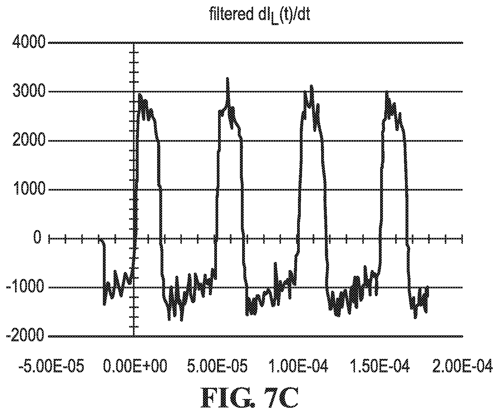
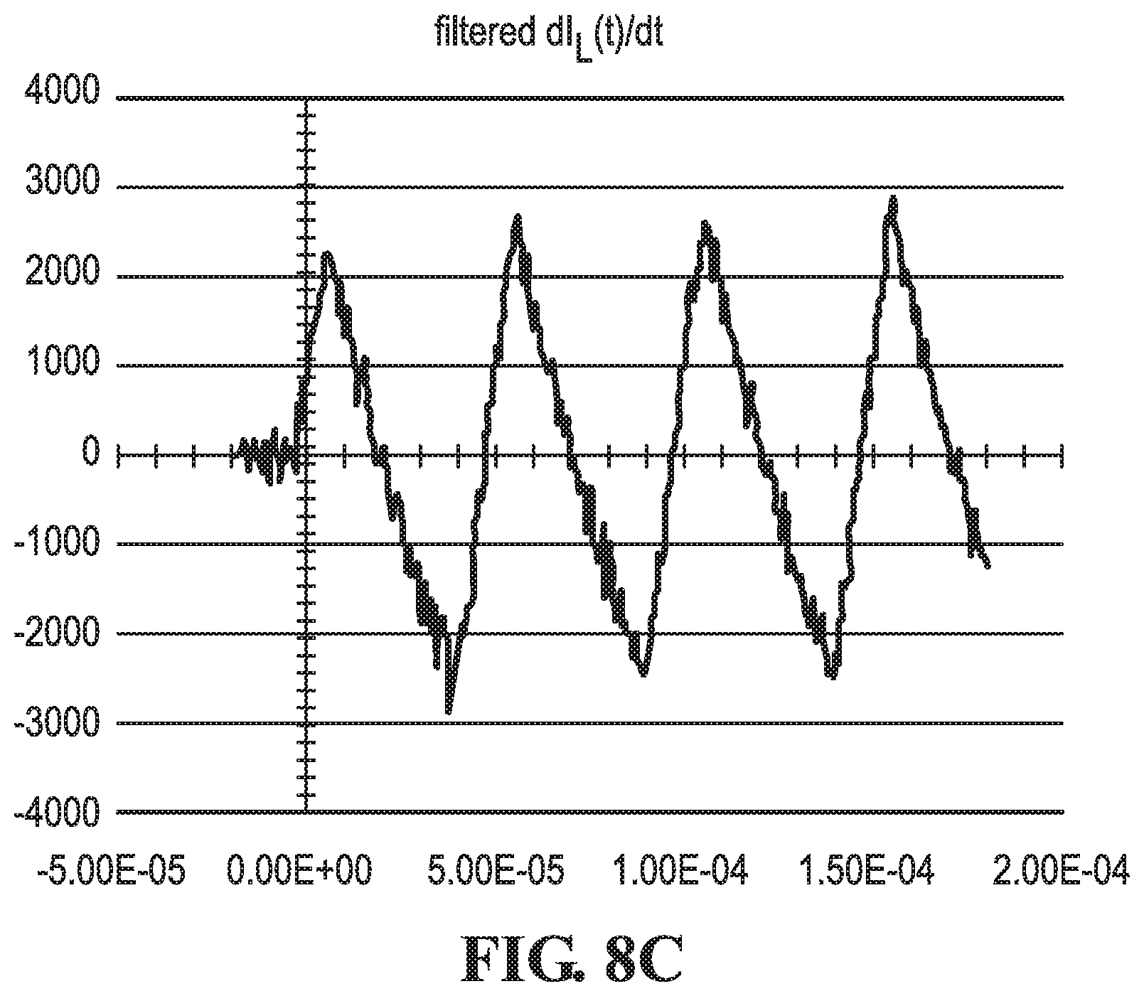
FIGS. 7A-7C demonstrates excitation characteristics for a dominantly inductive wire load, under an embodiment.
FIGS. 8A-8C demonstrates excitation characteristics for a dominantly inductive wire load, under an embodiment.
FIGS. 9A-9C demonstrate excitation characteristics for a for a dominantly resistive long wire load, under an embodiment.
FIGS. 10A-10C demonstrate excitation characteristics for a for a dominantly resistive long wire load, under an embodiment.
FIG. 11 shows reference current I.sub.L(t) resulting from the discrete time function I.sub.L(n.DELTA.t), under an embodiment.
FIG. 12 shows phasor .PHI.(n.DELTA.t) rotating about a unit circle, under an embodiment.
FIG. 13 shows the frequency content of a desired current provided by a discrete time function, under an embodiment.
FIG. 14 shows a first carrier component of a desired current, under an embodiment.
FIG. 15 shows a second carrier component of a desired current, under an embodiment.
FIG. 16 shows a two carrier approximation of a desired current, under an embodiment.
FIG. 17 shows voltage amplitudes V.sub.out and V.sub.C as a function of time (seconds), under an embodiment.
FIG. 18 shows a transmit circuit, under an embodiment.
FIG. 19 shows a voltage step waveform, under an embodiment.
FIG. 20 shows a voltage signal resulting from a voltage step waveform, under an embodiment.
FIG. 21 shows a graph of an impedance vector, under an embodiment.
FIG. 22 shows a voltage signal generated by the transmit circuit, under an embodiment.
FIG. 23 shows a graph of an impedance vector, under an embodiment.
FIG. 24 shows a graph of an impedance vector, under an embodiment.
FIG. 25 shows a graph of an impedance vector, under an embodiment.
DETAILED DESCRIPTION
An electronic animal containment system is described with direction-of-approach determination, or direction-sensitive capabilities. The direction-sensitive animal containment system generally contains a transmitter unit connected to a wire loop bounding a containment area and a receiver unit carried by the animal. The transmit unit provides certain properties in transmit waveforms for use by a companion receiver in determining direction of approach relative to the wire loop bounding the containment area.
Multiple embodiments of an electronic animal containment system provide varying methods for generating the required current in the wire loop. Under one embodiment, a containment signal generator may convert an uneven duty cycle square wave into an asymmetric triangle wave. Under another embodiment, a containment signal generator includes a discrete triangle wave generator allowing the adjustment of the rising and falling slopes. Under this embodiment, the discrete triangle wave generator directly drives the output current drivers and provides two amplitude levels for the triangle waveform.
Under either embodiment, the circuit parameters, L.sub.total and R.sub.total determine the generating signal required to produce the desired current by the equation:
.function..function..function. ##EQU00001## A companion receiver is responsive to: V.sub.receive(t)=K.sub.Rx*d.beta./dt (2) where
d.beta./dt is the rate of change of the magnetic flux density; d.beta./dt is dependent upon dI(t)/dt
K.sub.Rx=-n*A*u.sub.c-Rx
n=number of turns in the receive core
A=area of the receive core (m.sup.2)
u.sub.c-Rx=geometry dependent relative permeability of the receive core
Under one embodiment of an electronic animal containment system, a containment signal generator produces an uneven duty cycle square wave. A long wire load (or perimeter boundary wire) connected to the transmitter may result in an asymmetric triangle current flowing through the wire. This is true when the load is predominantly inductive under an embodiment, hence:
.function..function..function..function. ##EQU00002## Under this specific condition, an uneven duty cycle square wave will produce the desired asymmetry in the wire current.
Under another embodiment, a containment signal generator includes a discrete triangle wave generator allowing the adjustment of the rising and falling slopes. The discrete triangle wave generator directly drives the output current drivers and provides two amplitude levels for the triangle waveform. However, the desired asymmetry is produced only when the load is predominantly resistive under an embodiment, hence: V.sub.generator(t)=R.sub.total*I.sub.desired(t) (5) I.sub.desired(t)=V.sub.generator(t)/R.sub.total (6) Under this specific condition a discrete triangle wave generator with adjustable rising and falling slopes produce the desired asymmetry. Magnetic Field Relationships Between the Transmitter and Receiver System Model
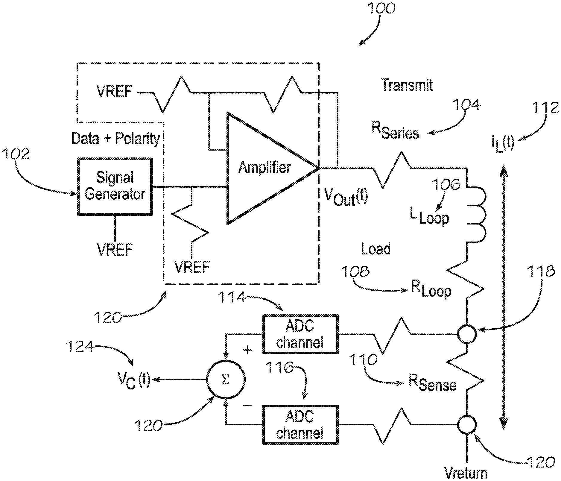
FIG. 1 shows the components of a transmit circuit 100. FIG. 1 shows a signal generator 102 connected to an amplifier 120. The amplifier is connected to transmit components comprising resistor R.sub.series 104, which is in series with inductor L.sub.Loop 106, which is in series with resistor R.sub.Loop 108, which is in series with resistor R.sub.sense 110. The transmit components are indicated in bold as shown in FIG. 1. Current I.sub.L (t) 112 flows through the transmit components. The amplifier 120 may be any amplifier topology with sufficient power output capability to produce V.sub.out(t) and I.sub.L (t) for the given load. Note that V.sub.out(t) is given by the following equation: V.sub.out(t)=(R.sub.series+R.sub.Loop+R.sub.sense)*I.sub.L(t)+L.sub.Loop*- dI.sub.L(t)/dt. (7)
FIG. 1 also shows analog-to-digital convertors 114 and 116 respectively connected to the transmit loop at points 118 and 120. An analog-to-digital converter (ADC) is a device that converts a continuous physical quantity (in this case, I.sub.L(t) produces a voltage across R.sub.sense) to a digital number that represents the quantity's amplitude. The conversion involves quantization of the input, so it necessarily introduces a small amount of error. Furthermore, instead of continuously performing the conversion, an ADC does the conversion periodically, sampling the input. The result is a sequence of digital values that have been converted from a continuous-time and continuous-amplitude analog signal to a discrete-time and discrete-amplitude digital signal. The summation component 120 of the transmit circuit combines the voltage amplitude at point 118 and point 120 to approximate the voltage drop across R.sub.sense, i.e. V.sub.C(t) 124.
FIG. 2 shows the components of a receive circuit 200. FIG. 2 shows interference 202 and time varying magnetic flux density,
.times..times..beta. ##EQU00003## 204 presented to the receive components. V.sub.sensor(t) 206 is the voltage rendered by the receive R-L-C circuit. The receive components include inductor L.sub.s 208 and resistor R.sub.s 210 in series. The receive components are in parallel with resistor R.sub.L 212 and capacitor C.sub.RES 214 which are in series with each other. The parallel circuit components are also in series with capacitor C 216. Points 220 and 222 represent respective inputs for Z Amplifier 230, Y Amplifier 240, and X Amplifier 250. VZ.sub.Receive(t) 260 represents the output voltage of the Z Amplifier. VY.sub.Receive(t) 270 represents the output voltage of the Y Amplifier. VX.sub.Receive(t) 280 represents the output voltage of the X Amplifier. Typically, the inductors, Ls, associated with each amplifier circuit (X, Y, and Z) are oriented orthogonal to one another. Note that for the sake of simplicity, the systems and methods described below refer to a single amplifier of a receiver. V.sub.Rx sensor(t) indicates the amplifier input voltage under an embodiment. V.sub.Receive(t) represents amplifier output voltage. Magnetic Field Relationships
FIG. 3 shows the time varying magnetic flux density generated by a current in a long wire. FIG. 3 shows an inductor L.sub.L 302 in series with a resistor R.sub.L 304 which reflect the circuit model for a long wire under an embodiment. FIG. 3 shows current I.sub.L 306. The point x 308 represents the distance to the wire in meters. The point X 310 shows the magnetic flux density travelling into the page. The time varying magnetic flux density is governed by the following equations:
.times..pi..times..times. ##EQU00004## .function..times..times..times..times. ##EQU00004.2## .times..times..times..times..times..times. ##EQU00004.3## .beta..function..function..times..times..times..pi..times..times. ##EQU00004.4## The time varying flux density at point x is specifically given by d.beta./dt=dI.sub.L(t)/dt*(u.sub.0/2.pi.x) (8)
FIG. 4 shows time varying magnetic flux density generated by a current in a multi-turn air core loop. FIG. 4 shows the direction of the time varying magnetic flux density 402. The multi-turn air core loop 404 comprises n turns, n.sub.L. Current I.sub.L enters the page at points 408 and exits the page at points 406. The coil 404, i.e. each loop turn, comprises a radius r.sub.L 410. The time varying magnetic flux density at a point x along the coil axis shown is governed by the following equations:
.beta..function..times. ##EQU00005## .times..times..beta..function..times. ##EQU00005.2## .function..times..times..times..times. ##EQU00005.3## .times..pi..times..times. ##EQU00005.4## .times..times..times..times. ##EQU00005.5##
The time varying flux density at point x along the coil axis is specifically given by d.beta./dt=dI(t)/dt*n.sub.L*u.sub.0*r.sub.L.sup.2/(2(r.sub.L.sup.2+x.sup.- 2).sup.3/2) (9)
FIG. 5 shows time varying magnetic flux density 502 generated by a current in a multi-turn ferrite core loop 504. The ferrite core loop comprises n turns, n.sub.L 506. The coil 504, i.e. each loop turn, comprises a radius r.sub.L 508. FIG. 5 shows the direction of the time varying magnetic flux density 502 and direction of current I.sub.C 510. The time varying magnetic flux density at a point x along the coil axis is governed by the following equations:
.times..beta..function..times. ##EQU00006## .times..times..times..beta..function..times. ##EQU00006.2## .times..function..times..times..times..times. ##EQU00006.3## .times..times..pi..times..times. ##EQU00006.4## .times..times..times..times..times..times..times..times..times..times..ti- mes..times..times..times..times..times..times..times..times..times..times.- .times..times..times..times..times. ##EQU00006.5## .times..times..times..times..times. ##EQU00006.6## The time varying flux density at point x along the coil axis is specifically given by d.beta./dt=dI.sub.L(t)/dt*u.sub.c-Tx*n.sub.L*u.sub.0r.sub.L.sup.2/(2(r.su- b.L.sup.2+x.sup.2).sup.3/2) (10) Receiver Output Voltage
Receive sensor output voltage results from proximity to a time varying magnetic flux density. FIG. 6 show an "n" turn 602 loop antenna 604 with area "A" 608. Note that the area A represents the area of one loop antenna turn. The upwardly directed arrows represent time varying magnetic flux density 610. The parameter .alpha. 620 represents the angle between horizontal line 622 and the loop antenna. The receive sensor output voltage is given by
.times..times..times..PHI..function..times..times..times..beta. ##EQU00007## .times..times..times..times..times..times..times..times..beta..times. ##EQU00007.2## .times..times..times..times..times..times..times..times..beta..function..- times..times..beta. ##EQU00007.3## .function. ##EQU00007.4## Note that N is a geometry dependent demagnetizing factor, and u.sub.r is the relative permeability of the receive core. A small N results in u.sub.c-Rx that approaches u.sub.r.
This particular receiver sensor output voltage, V.sub.Rx Sensor(t) is given by:
.times..times..times..function..times..times..beta..times..times..times..- function..times..times..beta..times..times..times..times..times..function.- .times..times..times..times..times..times..times..times..times..times..tim- es..times..times..times..times..times..times..times..times..times..times..- times..times..times..times..times..times..times..times..times..times..time- s..times..times..times..times..times..times..times..times..times..times..t- imes..times..times..times..times..times. ##EQU00008##
As shown above, the sensor output is proportional to d.beta.(t)/dt. However, d.beta.(t)/dt is dependent on the source of the time varying magnetic field (i.e. long wire, air coil, ferrite coil, etc.)
For a long wire:
.times..times..beta..function..times..pi..times..times..times..times..bet- a..function..times..times..times..times..times..times..pi..times..times..t- imes..times..times..times..times..times..times..times..times..times..times- ..times..times..times..times..times..times..pi..times..times. ##EQU00009##
For multi-turn air core loop: d.beta./dt=dI(t)/dt*n.sub.L*u.sub.0r.sub.L.sup.2(r.sub.L.sup.2+x.sup.2).s- up.3/2) (15) d.beta./dt=dI(t)/dt*(K.sub.Tx-coil air) (16) where,
n.sub.L=number of turns
r.sub.L=radius of the mult-turn transmit coil loop
K.sub.Tx-coil air=n.sub.L*u.sub.0*r.sub.L.sup.2/(2(r.sub.L.sup.2+x.sup.2).sup.3/2)
For a multi-turn ferrite core loop: d.beta./dt=dI.sub.L(t)/dt*u.sub.c-Tx*n.sub.L*u.sub.0*r.sub.L.sup.2/(2(r.s- ub.L.sup.2+x.sup.2).sup.3/2) (17) d.beta./dt=dI.sub.L(t)/dt*K.sub.Tx-coil ferrite (18) where u.sub.C-Tx=geometry dependent relative permeability of the transmit core K.sub.Tx-coil ferrite=u.sub.c-Tx*n.sub.L*u.sub.0*r.sub.L.sup.2/(2(r.sub.L.sup.2+x.sup.2- ).sup.3/2) (20) The receive sensor plus amplifier output voltage, V.sub.Receive(t), can be generalized as V.sub.Receive(t)=Gain.sub.amp(F.sub.C)*V.sub.Rx Sensor(t)=Gain.sub.amp(F.sub.C)*K.sub.Rx*d.beta./dt (21) V.sub.Receive(t)=Gain.sub.amp(F.sub.C)*dI.sub.L(t)/dt*K.sub.Rx*(K.sub.Tx(- #)) (22) where, Gain.sub.amp(F.sub.C)=the amplifier gain at the frequency of interest K.sub.Rx==n*A*u.sub.C-Rx (constant receive terms) n=number of turns in the receive core A=area of the receive core (m.sup.2) u.sub.C-Rx=geometry dependent relative permeability of the receive core K.sub.Tx(#) is dependent on the source of the time varying magnetic field Therefore, an observable asymmetric property in dI.sub.L(t)/dt, is preserved in V.sub.Receive(t). The asymmetry may be exploited by the companion receiver to indicate the direction of approach.
The desired transmit current contains an asymmetry in dI.sub.L(t)/dt that permits a receiver to determine direction of approach. The dI.sub.L(t)/dt asymmetry is observed as a difference between the positive and negative time duration and/or a difference in the positive and negative peak values at the output of the receiver sensor and amplifier chain.
FIG. 7 and FIG. 8 demonstrate excitation characteristics for a dominantly inductive wire load. FIGS. 7A-7C show an example of square wave excitation under an embodiment. FIG. 7A shows load voltage V(t) of a transmitter as a function of time (seconds). FIG. 7B displays the corresponding load current. In particular, FIG. 7B shows the filtered load current I.sub.L as a function of time (seconds). FIG. 7C shows the filtered rate of change in load current dI.sub.L(t)/dt as a function of time (seconds). FIGS. 8A-8C shows an example of triangle wave excitation under an embodiment. FIG. 8A shows the load voltage V(t) of a transmitter as a function of time (seconds). FIG. 8B displays the corresponding load current. In particular, FIG. 8B shows the filtered load current I.sub.L as a function of time (seconds). FIG. 8C shows the filtered rate of change in load current dI.sub.L(t)/dt as a function of time (seconds). Note from FIG. 7 and FIG. 8 that for dominantly inductive long wire loads, the desired asymmetry in dI.sub.L(t)/dt occurs for square wave excitation.
FIG. 9 and FIG. 10 demonstrate excitation characteristics for a dominantly resistive long wire load. FIGS. 9A-9C show an example of square wave excitation under an embodiment. FIG. 9A shows load voltage V(t) of a transmitter as a function of time (seconds). FIG. 9B displays the corresponding load current. In particular, FIG. 9B shows the filtered load current I.sub.L as a function of time (seconds). FIG. 9C shows the filtered rate of change in load current dI.sub.L(t)/dt as a function of time (seconds). FIGS. 10A-10C show an example of triangle wave excitation under an embodiment. FIG. 10A shows the load voltage V(t) of a transmitter as a function of time (seconds). FIG. 10B displays the corresponding load current. In particular, FIG. 10B shows the filtered load current I.sub.L as a function of time (seconds). FIG. 10C shows the filtered rate of change in load current dI.sub.L(t)/dt as a function of time (seconds). Note from FIG. 9 and FIG. 10 that for dominantly resistive long wire loads, the desired asymmetry in dI.sub.L(t)/dt occurs for asymmetric triangle wave excitation.
System, Method, and Apparatus for Constructing Voltage Excitation Waveform
Discrete Time Function
Under one embodiment, a discrete time function, I.sub.L(n.DELTA.t) is created which describes the desired load current asymmetry. Under an embodiment, the desired asymmetry is a triangle current waveform with different positive and negative slopes. FIG. 11 shows reference current I.sub.L(t) resulting from the discrete time function I.sub.L(n.DELTA.t) as further described below.
OOK (On Off Keying) or amplitude modulation (amplitude shift keying) is used to modulate (or impart data onto) the discrete time function I.sub.L(n.DELTA.t) as further described below. The modulation function is referred to as modulation(n.DELTA.t) and resolves to either one or zero under an embodiment.
Rotating phasor values, expressed as .PHI.(n.DELTA.t)=.omega.n.DELTA.t (modulo 2.pi.), are used to generate the discrete time function I.sub.L(n.DELTA.t) as further described below.
The discrete time function I.sub.L(n.DELTA.t) comprises a desired asymmetry of 30%. Symmetry test thresholds for .PHI.(n.DELTA.t) are as follows:
s.sub.1=0.942478 radians
s.sub.2=5.340708 radians
Using these test thresholds, the region of positive slope comprises 30% of 2.pi. radians.
FIG. 12 shows phasor .PHI.(n.DELTA.t) rotating about a unit circle with a frequency, f. Note that angular frequency .omega. (rads/sec)=2.pi.f. FIG. 12 shows symmetry test threshold s.sub.1=0.942478 and s.sub.2=5.340708. FIG. 12 displays a region of positive slope 1210 and a region of negative slope 1220 that result in the desired asymmetry.
The desired positive slope m.sub.1 of I.sub.L(n.DELTA.t) comprises change in amplitude/change in .PHI.(n.DELTA.t). The desired positive slope of I.sub.L(n.DELTA.t) is m.sub.1=2/(2*s.sub.1). The desired negative slope m.sub.2 of I.sub.L(n.DELTA.t) comprises change in amplitude/change in .PHI.(n.DELTA.t). The desired negative slope of I.sub.L(n.DELTA.t) is m.sub.2=-2/(2.pi.-2*s.sub.1).
The discrete time function, I.sub.L(n.DELTA.t) is given by the following logic:
TABLE-US-00001 (23) if (modulation(n.DELTA.t) != 0) if (.PHI.(n.DELTA.t) >= s.sub.2 OR .PHI.(n.DELTA.t) < s.sub.1), // region of positive slope if (.PHI.(n.DELTA.t) < s.sub.1), .DELTA..PHI. = .PHI.(n.DELTA.t) + s.sub.1 else .DELTA..PHI. = .PHI.(n.DELTA.t) - s.sub.2 I.sub.L(n.DELTA.t) = (modulation(n.DELTA.t) * .DELTA..PHI. * m.sub.1 ) - 1 else // region of negative slope, .DELTA..PHI. = .PHI.(n.DELTA.t) - s.sub.1 I.sub.L(n.DELTA.t) = (modulation(n.DELTA.t) * .DELTA..PHI. * m.sub.2 ) + 1 else I.sub.L(n.DELTA.t) = 0 // no modulation
FIG. 13 shows the frequency content of the desired current provided by the discrete time function, I.sub.L(n.DELTA.t), when f=20,000 Hz. FIG. 13 provides the results of Discrete Fourier Transform analysis. The figure shows a first harmonic at a frequency of 20,000 Hz and with relative amplitude 53 db. The figure shows a second harmonic at a frequency of 40,000 Hz and with relative amplitude of 43 db. The figure shows a third harmonic at a frequency of 60,000 Hz and with relative amplitude of 30 db. The relative harmonic relationships of the desired I.sub.L(n.DELTA.t) are:
TABLE-US-00002 Harmonic: Relative Amplitude: Relative Phase (rads): 1st 1 0 2nd 0.3060 0 3rd 0.0819 0
Practical limitations of the DFT algorithm permit showing only the first three harmonics. In practice, the harmonics continue indefinitely. Approximate Current Using First and Second Harmonics
The desired current may then be approximated using only the first and second harmonics. FIG. 14 shows a first carrier I.sub.FC(n.DELTA.t) component of the desired current using the first relative amplitude of the first harmonic. FIG. 15 shows a second carrier I.sub.2FC(n.DELTA.t) component of the desired current using the relative amplitude of the second harmonic. Again note that the relative amplitude of the first and second harmonics are 1.00 and 0.3060 respectively. Therefore, a two carrier approximation to I.sub.L(n.DELTA.t) (shown in FIG. 16) is given by AI.sub.L(n.DELTA.t)=sin(.omega.n.DELTA.t)+0.3060*sin(2.omega.n.DELTA.t- ) (24)
where,
f=20,000 Hz
.omega.=2.pi.f
The sample rate, 1/.DELTA.t, is left to the discretion of the system designer but should be high enough (i.e. =>8.times. the fundamental frequency) to achieve the desired precision. The sampling rate used in this example is 160,000 Hz, i.e. 8*f. With only two terms, the operations required to realize the approximation are easy to perform in a low cost commercial microprocessor using either batch or real time processing algorithms.
Iterative, Adaptive, Feedback Control Algorithm
Derive an Estimate of the Loop Inductance (L.sub.Loop) and Loop Resistance (R.sub.Loop)
Under one embodiment, an estimate of the loop inductance (L.sub.Loop) and loop resistance (R.sub.Loop) are derived. Reference is made to the transmit circuit shown in FIG. 1. The transmit circuit of FIG. 1 is excited with a reference step and the response V.sub.C(t) is analyzed. FIG. 17 shows voltage amplitudes V.sub.out [.about.2V] and V.sub.C [.about.0.75V] as a function of time (seconds).
.function..times..times..function..times..times..times. ##EQU00010##
For a long wire circuit employed under the embodiment described herein, the R.sub.series is in the range of 90-180 ohms and R.sub.sense is 30 ohms.
Averaging multiple measurements yields a good approximation of R.sub.Loop under an embodiment. The transmit loop time constant may be used to approximate the value of L.sub.Loop. The transmit loop time constant may be expressed as T.sub.C=L/R. In one time constant T.sub.C=L/R), V.sub.C(t) reaches 63.2% of its final value. Under an embodiment, the elapsed time, .DELTA.t1, is recorded when V.sub.C(t) reaches 63.2% of its final value. In two time constants, V.sub.C(t) reaches 86.5% of its final value. Under an embodiment, the elapsed time, .DELTA.t2, is recorded when V.sub.C(t) reaches 86.5% of its final value. L.sub.Loop is calculated as follows: L.sub.Loop=R.sub.Circuit*.DELTA.t1 (27) L.sub.Loop=R.sub.Circuit*.DELTA.t2/2 (28) where R.sub.circuit=R.sub.series R.sub.sense R.sub.Loop. Averaging multiple measurements yields a good approximation of L.sub.Loop.
The measurement interval can be long (as compared to the interval between data transmissions) and left to the discretion of the system designer. In general, changes in the loop parameters (other than an open circuit) do not occur suddenly. Open circuits can be detected by observing V.sub.C(t) during all other active periods.
Scale the Approximation AI.sub.L(n.DELTA.t) and Calculate First Iteration of V.sub.Gen(n.DELTA.t).
A working animal containment system requires a minimum receive signal at a distance x from the transmit loop. Under an embodiment, the necessary amplitude of the two carrier approximation, AI.sub.L(n.DELTA.t) is calculated. V.sub.Receive-required=Gain.sub.sensor+amp(F.sub.C,2F.sub.C)*V.sub.Sensor- -required (29) V.sub.Receive-required=Gain.sub.sensor+amp(F.sub.C,2F.sub.C)*.DELTA.I.sub- .L/.DELTA.t_required*K.sub.Rx*KT.sub.x(#) (30) .DELTA.I.sub.L/.DELTA.t_required=V.sub.Receive-required/(Gain.sub.sensor+- amp(F.sub.C,2F.sub.C)*K.sub.RxK.sub.Tx(#)) (31) where, Gain.sub.sensor+amp (F.sub.C, 2.sub.FC)=sensor plus amplifier gain at the frequency or band of interest. K.sub.Rx=n*A*u.sub.C-Rx K.sub.Tx(#)=is dependent on the distance, x, and the source type.sup.1 .DELTA.=the discrete time differentiation operator .sup.1 It is either K.sub.Tx-long wire, K.sub.Tx-coil air, or K.sub.Tx-coil ferrite. Under the embodiment described below,
V.sub.Receive-required.about.18.6 mVRMS
Gain.sub.sensor+amp (F.sub.C, 2F.sub.C).about.2550
n.about.950
A.about.1.164e--5 square meters
u.sub.(c-Rx).about.5.523
The sensor plus amplifier needs to be responsive from F.sub.C to 2F.sub.C. A relatively flat response is ideal, but other response characteristics (gain and phase) may be compensated for by digital signal processing in the receiver's microprocessor.
Under an embodiment, solve for the load current scaling factor, K.sub.I: .DELTA.I.sub.L/.DELTA.t_required=K.sub.I*.DELTA.AI.sub.L/.DELTA.t_peak (32) K.sub.I=.DELTA.I.sub.L/.DELTA.t_required/(.DELTA.AI.sub.L/.DELTA.t_p- eak). (33) The resulting loop current is therefore, AI.sub.L(n.DELTA.t)=K.sub.I*(sin(.omega.n.DELTA.t)+0.3060*sin(2.omega.n.D- ELTA.t)). Under an embodiment, V.sub.Gen(n.DELTA.t) is calculated using Kirchhoff s law, i.e. by V.sub.Gen(n.DELTA.t)=K.sub.I*(R.sub.circuit*AI.sub.L(n.DELTA.t)+L.sub.Loo- p*.DELTA.AI.sub.L(n.DELTA.t)/.DELTA.t)). (34) Under one embodiment the first iteration of the signal generator voltage waveform, V.sub.Gen(n.DELTA.t), may be employed as the generator signal for system operation. One may stop here if there is high confidence the estimated loop parameters adequately reflect the circuit operating conditions for achieving the desired amplitude and asymmetry. Observe V.sub.C(n.DELTA.t) for the Desired Characteristics in the Transmit Loop Current AI.sub.L(n.DELTA.t)
Under an embodiment, one may observe V.sub.C(n.DELTA.t) for the desired characteristics in the transmit loop current AI.sub.L(n.DELTA.t). FIG. 18 shows the same transmit circuit as displayed in FIG. 1 with additional elements to model the receiver signal processing using V.sub.C(n.DELTA.t). As seen in FIG. 18, the V.sub.C(n.DELTA.t) signal outputs to a digital component 130 that approximates the Receiver (Rx) Sensor Response. The digital approximation is sufficiently modeled as a single pole high pass filter (f.sub.corner=2525 Hz) followed by a single pole low pass filter (f.sub.corner=38870 Hz) and a gain of 2550. As seen in FIG. 18, the digital approximation component 130 outputs to the Receiver (Rx) Detection Component/Algorithm 132. The receiver detection component/algorithm generates the weighted and time shifted sum of two bandpass filter outputs. One centered at the fundamental carrier frequency and one centered at 2.times. the fundamental carrier frequency. A relative time shift between the two filter outputs is required to match the difference in group delay through each bandpass filter. The receiver detection algorithm (also referred to as the feedback detection algorithm) estimates the root means square, V.sub.Rx-RMS 134 (at the required distance measured in Analog-to-Digital-Converter counts) and Rx Asymmetry Value 136 (ratio of the aggregate negative to positive signal peaks) of the receive signal.
Under one embodiment, an adaptive feedback algorithm seeks a solution to satisfy both the minimum receive signal, V.sub.Receive(n.DELTA.t), and the desired receive asymmetry. In this illustrative example, the desired receive asymmetry will be the ratio of the aggregate positive and aggregate negative peaks of V.sub.Receive(n.DELTA.t).
The two frequency transmit current, .DELTA.I.sub.L(n.DELTA.t), can be derived from the observed V.sub.C(n.DELTA.t) and R.sub.Sense. AI.sub.L(n.DELTA.t)=V.sub.C(n.DELTA.t)/R.sub.Sense (35) .DELTA.AI.sub.L(n.DELTA.t)/.DELTA.t=[.DELTA.AI.sub.L(n.DELTA.t)-.DELTA.AI- .sub.L(n.DELTA.(t-1))]/.DELTA.t. (36)
The illustrative example that follows is for a long wire (approximately 2500 ft. of 16AWG wire, at an operating frequency of 25000 Hz), where: .DELTA..beta./.DELTA.t=.DELTA.AI.sub.L(n.DELTA.t)/.DELTA.t*(u.sub.0/2.pi.- x) (37) where, x=3 meters.
The receive sensor plus amplifier output voltage, V.sub.Receive(t), can be generalized as
.function..function..times..function..function..times..times..beta..times- ..function..function..function..times..times..DELTA..times..times..DELTA..- times..times..function..times..times..times..times..times..function..times- ..times..times..times..times..times..times..times..times..times..times..ti- mes..times..times..times..times..times..times..times..times..times..times.- .times..times..times..times..times..times..times..times..times..times..tim- es..times..times..times..times..times..times..times..times..times..times..- times..times..times..times..times..times..times..times..times..times..time- s..times..times..times..times..times..times..times..times..times..times..t- imes..times..times..times..times..function..times..times..times..times..ti- mes..times..times..times..times..times..times..times..times..times..times.- .times..times..times..times..times..times..times. ##EQU00011## First, the load parameters are estimated by the previously described analysis of V.sub.C(n.DELTA.t) when applying a step waveform. FIG. 19 shows a step waveform V.sub.GEN(n.DELTA.t) reaching voltage of approximately 0.44 volts. FIG. 20 shows the corresponding signal V.sub.C(t) reaching a voltage of approximately 1.4 volts.
R.sub.LOOP and R.sub.CIRCUIT values are then estimated as follows.
R.sub.Loop estimate=17.568.OMEGA.
L.sub.Loop estimate=0.001382 H
R.sub.circuit=R.sub.Series+R.sub.Sense+R.sub.Loop estimate=195.393
L.sub.Circuit=L.sub.Loop estimate=0.001382 H
Under one embodiment, an iterative examination of V.sub.GEN(n.DELTA.t) begins with feedback algorithm goals as follows.
V.sub.Rx-RMS.sub.(at required distance measured in A/D Converter counts)=7.619+/-6.5%
Rx Asymmetry Ratio.sub.(ratio of the aggregate negative to positive signal peaks)=1.692+/-8.55%
The signal generator transmit provides the initial V.sub.Gen-0(N.DELTA.t) signal to a transmit circuit comprising starting point circuit parameters of an iterative adaptive feedback algorithm. The starting point circuit parameters, Z(0), under an embodiment are:
R.sub.Circuit=195.393.OMEGA.
L.sub.Loop=0.001382 H
FIG. 21 shows the initial impedance vector Z(0).
FIG. 22 shows V.sub.Gen-0(n.DELTA.t)=K.sub.I*(R.sub.Circuit*AI.sub.L(n.DELTA.t)+L.sub.L- oop*.DELTA.AI.sub.L(n.DELTA.t)/.DELTA.t)).
The feedback detection algorithm (see FIG. 18) produces the following receive model output results for V.sub.Gen-0(n.DELTA.t):
V.sub.Rx-RMS estimate=8.571
Rx Asymmetry estimate=1.519
The receive signal RMS is not within the acceptable range under an embodiment. When the RMS is not within limits, a scalar gain adjustment is needed. The feedback algorithm will scale the circuit impedance vector accordingly. The scalar gain adjustment is described as follows: Scalar gain adjustment:
Z=.omega.L+R
Z(n)=Z(n-1)*V.sub.Rx-RMS goal/V.sub.Rx-RMS estimate
for this example:
R.sub.Circuit(1)=195.393.OMEGA.*7.619/8.571=173.690.OMEGA.
L.sub.Loop(1)=0.001382 H*7.619/8.571=0.0012285 H=0.001229 H
Under an embodiment, the previously iterated circuit parameters are now:
R.sub.circuit=173.6901.OMEGA.
L.sub.Loop=0.001229 H
FIG. 23 shows a graph of the impedance vector Z(1).
The V.sub.Gen-1(n.DELTA.t) signal is then applied to the transmit circuit, where V.sub.Gen-1(n.DELTA.t)=K.sub.I*(R.sub.circuit*AI.sub.L(n.DELTA.t)+L.sub.L- oop*.DELTA.AI.sub.L(n.DELTA.t)/.DELTA.t)).
The feedback detection algorithm produces the following receive model output results for V.sub.Gen-1(n.DELTA.t):
V.sub.Rx-RMS estimate=7.546
Rx Asymmetry estimate=1.532
The receive signal asymmetry is not within the acceptable range under an embodiment. When no gain adjustment is required and the asymmetry is not within limits, an impedance vector rotation is needed. The first rotation in an iteration sequence is assumed to be positive. The feedback algorithm will rotate the circuit impedance vector accordingly.
The Z(1) impedance vector has an angle of 48.01 degrees. There is no correlation between the asymmetry error and the proper rotation direction. Our first rotation is assumed to be positive and we rotate one-sixth (1/6) of the degrees between our current angle and 90 degrees. Hence we rotate Z(1) by 7 degrees. The new impedance vector shall have the same magnitude but at an angle of 55.01 degrees.
R(2)=Z(1) Magnitude*cosine(55.01 degrees)
.omega.L(2)=Z(1) Magnitude*sine(55.01 degrees)
therefore;
L(2)=.omega.L(2)/.omega..
Note that there is nothing sacred about rotating 1/6 of the degrees between the current angle and the hard boundary (0 or 90 degrees). It is a compromise between the number of iterations required to achieve a suitable end result, and the precision of the end result.
Under an embodiment, the previously iterated circuit parameters are now:
R.sub.circuit=148.884.OMEGA.
L.sub.Loop=0.001354 H
FIG. 24 shows a graph of the impedance vector Z(2).
The V.sub.Gen-2(n.DELTA.t) signal is then applied to the transmit circuit, where V.sub.Gen-2(n.DELTA.t)=K.sub.I*(R.sub.circuit*AI.sub.L(n.DELTA.t)+L.sub.L- oop*.DELTA.AI.sub.L(n.DELTA.t)/.DELTA.t)).
The feedback detection algorithm produces the following receive model output results for V.sub.Gen-2(n.DELTA.t):
V.sub.Rx-RMS estimate=7.546
Rx Asymmetry estimate=1.532
The receive signal asymmetry is not within the acceptable range under an embodiment. When no gain adjustment is required and the asymmetry is not within limits, an impedance vector rotation is needed. Positive rotation did not improve the asymmetry. Therefore, a negative rotation is used. The feedback algorithm will rotate the circuit impedance vector accordingly.
The Z(2) impedance vector has an angle of 55.01 degrees. Our first rotation was assumed to be positive. It did not improve the asymmetry result, therefore we must rotate in the negative direction. Rotate one-sixth (1/6) of the degrees between our current angle and 0 degrees. Hence we rotate Z(2) by 9.71 degrees. The new impedance vector shall have the same magnitude but at an angle of 45.84 degrees.
R(3)=Z(2) Magnitude*cosine(45.84 degrees)
.omega.L(3)=Z(2) Magnitude*sine(45.84 degrees)
therefore;
L(3)=.omega.L(3)/.omega..
Under an embodiment, the previously iterated circuit parameters are now:
R.sub.circuit=180.872.OMEGA.
L.sub.Loop=0.001186 H
FIG. 25 shows a graph of the impedance vector Z(3).
The V.sub.Gen-3 (n.DELTA.t) signal is then applied to the transmit circuit, where V.sub.Gen-3 (n.DELTA.t)=K.sub.I*(R.sub.circuit*AI.sub.L(n.DELTA.t)+L.sub.Loop*.DELTA.- AI.sub.L(n.DELTA.t)/.DELTA.t)).
The feedback detection algorithm produces the following receive model output results for V.sub.Gen-3(n.DELTA.t):
V.sub.Rx-RMS estimate=7.7092
Rx Asymmetry estimate=1.582
The receive signal RMS and asymmetry are within acceptable ranges. The adaptive feedback algorithm is complete under an embodiment. The correct circuit parameters for normal operation are:
R.sub.circuit=180.872.OMEGA.
L.sub.Loop=0.001186 H
Also notice that the circuit impedance vector for the 3.sup.rd and final iteration is neither predominantly inductive or resistive. Therefore, the required V.sub.Gen-3(n.DELTA.t) is neither an "uneven duty cycle square wave" nor a "triangle wave with adjustable slopes".
A method is described herein that comprises describing a load current with a discrete time function. The method includes using a first frequency and a second frequency to provide an approximation of the described load current, wherein a transform applied to the discrete time function identifies the first frequency and the second frequency. The method includes estimating a loop inductance and a loop resistance of a wire loop by exciting a transmit circuit with a voltage reference step waveform, wherein the transmit circuit includes the wire loop. The method includes scaling the approximated load current to a level sufficient to generate a minimum receive voltage signal in a receiver at a first distance between the wire loop and the receiver. The method includes generating a first voltage signal using the scaled load current, the estimated loop inductance, and the estimated loop resistance. The method includes exciting the transmit circuit with the first voltage signal.
The estimating the loop inductance and the loop resistance includes under an embodiment monitoring the transmit circuit's current in response to the voltage reference step waveform.
The monitoring the transmit circuit's current includes under an embodiment capturing current amplitude as a function of time in response to the voltage reference step waveform.
The transform comprises a Discrete Fourier Transform under an embodiment.
The first frequency comprises a first harmonic frequency of the described load current under an embodiment.
The second frequency comprises a second harmonic frequency of the described load current under an embodiment.
The method comprises under an embodiment generating a first carrier component of the approximated load current using the first harmonic frequency, wherein the first carrier component has a weight of one.
The method comprises under an embodiment generating a second carrier component of the approximated load current using the second harmonic frequency, wherein an amplitude of the second carrier component is weighted relative to an amplitude of the first carrier component.
The transform applied to the discrete time function used to describe the load current identifies under an embodiment the relative weight of the second carrier component.
The providing the approximation of the described load current includes summing the first carrier component and the second carrier component under an embodiment.
The approximated load current comprises a discrete time function under an embodiment.
The first voltage signal comprises a discrete time function under an embodiment.
An input to the discrete time function used to describe the load current comprises a rotating phasor under an embodiment.
The phasor value periodically rotates between 0 and 2.pi. radians under an embodiment.
The discrete time function used to describe the load current has a first slope when the phasor value is within a first range under an embodiment.
The first slope is positive under an embodiment.
The discrete time function used to describe the load current has a second slope when the phasor value is within a second range under an embodiment.
The second slope is negative under an embodiment.
The first range comprises approximately thirty percent of 2.pi. radians under an embodiment.
The absolute value of the first slope is greater than the absolute value of the second slope under an embodiment.
The method comprises under an embodiment reading a voltage signal at a location in the transmit circuit, wherein the voltage signal is representative of a corresponding transmit current in the transmit circuit.
The method comprises under an embodiment processing the voltage signal to estimate the receive voltage signal.
The estimating includes under an embodiment determining a root mean square (RMS) of the estimated receive voltage signal.
The estimating includes under an embodiment determining an asymmetry of the estimated receive voltage signal.
The asymmetry comprises under an embodiment a ratio of the aggregate positive and aggregate negative peaks of the estimated receive voltage signal.
The method comprises establishing a target RMS value under an embodiment.
A target RMS range comprises under an embodiment the target RMS value plus or minus a percentage.
The method of an embodiment comprises establishing a target asymmetry value.
A target asymmetry range comprises under an embodiment the target asymmetry value plus or minus a percentage.
The method under an embodiment comprises iteratively adjusting an impedance vector of the transmit circuit until the RMS and the asymmetry of estimated receive voltage signal fall within the corresponding target RMS and asymmetry ranges, wherein the impedance vector initially comprises the loop resistance and the loop inductance.
The adjusting comprises under an embodiment scaling the impedance vector when the RMS falls outside the target RMS range.
The adjusting comprises under an embodiment rotating a phase angle of the impedance vector when the asymmetry falls outside the target asymmetry range.
The rotating the phase angle comprising under an embodiment a negative rotation.
The rotating the phase angle comprises under an embodiment a positive rotation.
The described load current comprises an asymmetry under an embodiment.
The receiver exploits under an embodiment the asymmetry to determine the receiver's direction of approach to the wire loop carrying the described load current.
Computer networks suitable for use with the embodiments described herein include local area networks (LAN), wide area networks (WAN), Internet, or other connection services and network variations such as the world wide web, the public internet, a private internet, a private computer network, a public network, a mobile network, a cellular network, a value-added network, and the like. Computing devices coupled or connected to the network may be any microprocessor controlled device that permits access to the network, including terminal devices, such as personal computers, workstations, servers, mini computers, main-frame computers, laptop computers, mobile computers, palm top computers, hand held computers, mobile phones, TV set-top boxes, or combinations thereof. The computer network may include one or more LANs, WANs, Internets, and computers. The computers may serve as servers, clients, or a combination thereof.
The apparatus, systems and methods for generating voltage excitation waveforms can be a component of a single system, multiple systems, and/or geographically separate systems. The apparatus, systems and methods for generating voltage excitation waveforms can also be a subcomponent or subsystem of a single system, multiple systems, and/or geographically separate systems. The components of the apparatus, systems and methods for generating voltage excitation waveforms can be coupled to one or more other components (not shown) of a host system or a system coupled to the host system.
One or more components of the apparatus, systems and methods for generating voltage excitation waveforms and/or a corresponding interface, system or application to which the apparatus, systems and methods for generating voltage excitation waveforms is coupled or connected includes and/or runs under and/or in association with a processing system. The processing system includes any collection of processor-based devices or computing devices operating together, or components of processing systems or devices, as is known in the art. For example, the processing system can include one or more of a portable computer, portable communication device operating in a communication network, and/or a network server. The portable computer can be any of a number and/or combination of devices selected from among personal computers, personal digital assistants, portable computing devices, and portable communication devices, but is not so limited. The processing system can include components within a larger computer system.
The processing system of an embodiment includes at least one processor and at least one memory device or subsystem. The processing system can also include or be coupled to at least one database. The term "processor" as generally used herein refers to any logic processing unit, such as one or more central processing units (CPUs), digital signal processors (DSPs), application-specific integrated circuits (ASIC), etc. The processor and memory can be monolithically integrated onto a single chip, distributed among a number of chips or components, and/or provided by some combination of algorithms. The methods described herein can be implemented in one or more of software algorithm(s), programs, firmware, hardware, components, circuitry, in any combination.
The components of any system that include the apparatus, systems and methods for generating voltage excitation waveforms can be located together or in separate locations. Communication paths couple the components and include any medium for communicating or transferring files among the components. The communication paths include wireless connections, wired connections, and hybrid wireless/wired connections. The communication paths also include couplings or connections to networks including local area networks (LANs), metropolitan area networks (MANs), wide area networks (WANs), proprietary networks, interoffice or backend networks, and the Internet. Furthermore, the communication paths include removable fixed mediums like floppy disks, hard disk drives, and CD-ROM disks, as well as flash RAM, Universal Serial Bus (USB) connections, RS-232 connections, telephone lines, buses, and electronic mail messages.
Aspects of the apparatus, systems and methods for generating voltage excitation waveforms and corresponding systems and methods described herein may be implemented as functionality programmed into any of a variety of circuitry, including programmable logic devices (PLDs), such as field programmable gate arrays (FPGAs), programmable array logic (PAL) devices, electrically programmable logic and memory devices and standard cell-based devices, as well as application specific integrated circuits (ASICs). Some other possibilities for implementing aspects of the apparatus, systems and methods for generating voltage excitation waveforms and corresponding systems and methods include: microcontrollers with memory (such as electronically erasable programmable read only memory (EEPROM)), embedded microprocessors, firmware, software, etc. Furthermore, aspects of the apparatus, systems and methods for generating voltage excitation waveforms and corresponding systems and methods may be embodied in microprocessors having software-based circuit emulation, discrete logic (sequential and combinatorial), custom devices, fuzzy (neural) logic, quantum devices, and hybrids of any of the above device types. Of course the underlying device technologies may be provided in a variety of component types, e.g., metal-oxide semiconductor field-effect transistor (MOSFET) technologies like complementary metal-oxide semiconductor (CMOS), bipolar technologies like emitter-coupled logic (ECL), polymer technologies (e.g., silicon-conjugated polymer and metal-conjugated polymer-metal structures), mixed analog and digital, etc.
It should be noted that any system, method, and/or other components disclosed herein may be described using computer aided design tools and expressed (or represented), as data and/or instructions embodied in various computer-readable media, in terms of their behavioral, register transfer, logic component, transistor, layout geometries, and/or other characteristics. Computer-readable media in which such formatted data and/or instructions may be embodied include, but are not limited to, non-volatile storage media in various forms (e.g., optical, magnetic or semiconductor storage media) and carrier waves that may be used to transfer such formatted data and/or instructions through wireless, optical, or wired signaling media or any combination thereof. Examples of transfers of such formatted data and/or instructions by carrier waves include, but are not limited to, transfers (uploads, downloads, e-mail, etc.) over the Internet and/or other computer networks via one or more data transfer protocols (e.g., HTTP, FTP, SMTP, etc.). When received within a computer system via one or more computer-readable media, such data and/or instruction-based expressions of the above described components may be processed by a processing entity (e.g., one or more processors) within the computer system in conjunction with execution of one or more other computer programs.
Unless the context clearly requires otherwise, throughout the description and the claims, the words "comprise," "comprising," and the like are to be construed in an inclusive sense as opposed to an exclusive or exhaustive sense; that is to say, in a sense of "including, but not limited to." Words using the singular or plural number also include the plural or singular number respectively. Additionally, the words "herein," "hereunder," "above," "below," and words of similar import, when used in this application, refer to this application as a whole and not to any particular portions of this application. When the word "or" is used in reference to a list of two or more items, that word covers all of the following interpretations of the word: any of the items in the list, all of the items in the list and any combination of the items in the list.
The above description of embodiments of the apparatus, systems and methods for generating voltage excitation waveforms is not intended to be exhaustive or to limit the systems and methods to the precise forms disclosed. While specific embodiments of, and examples for, the apparatus, systems and methods for generating voltage excitation waveforms and corresponding systems and methods are described herein for illustrative purposes, various equivalent modifications are possible within the scope of the systems and methods, as those skilled in the relevant art will recognize. The teachings of the apparatus, systems and methods for generating voltage excitation waveforms and corresponding systems and methods provided herein can be applied to other systems and methods, not only for the systems and methods described above.
The elements and acts of the various embodiments described above can be combined to provide further embodiments. These and other changes can be made to the apparatus, systems and methods for generating voltage excitation waveforms and corresponding systems and methods in light of the above detailed description.
* * * * *
References
D00000
D00001
D00002
D00003
D00004
D00005
D00006
D00007
D00008
D00009
D00010
D00011
D00012

D00013
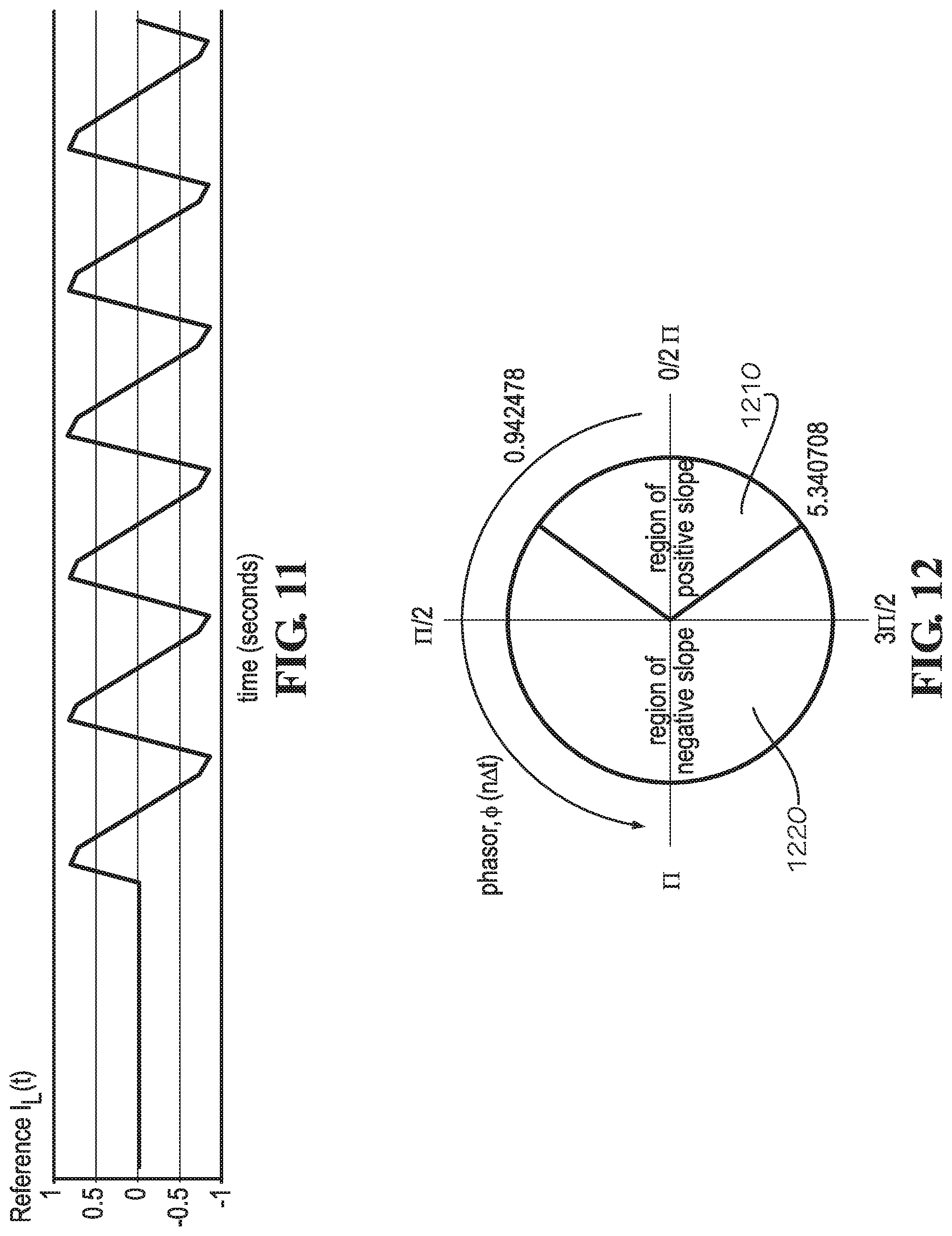
D00014

D00015

D00016

D00017
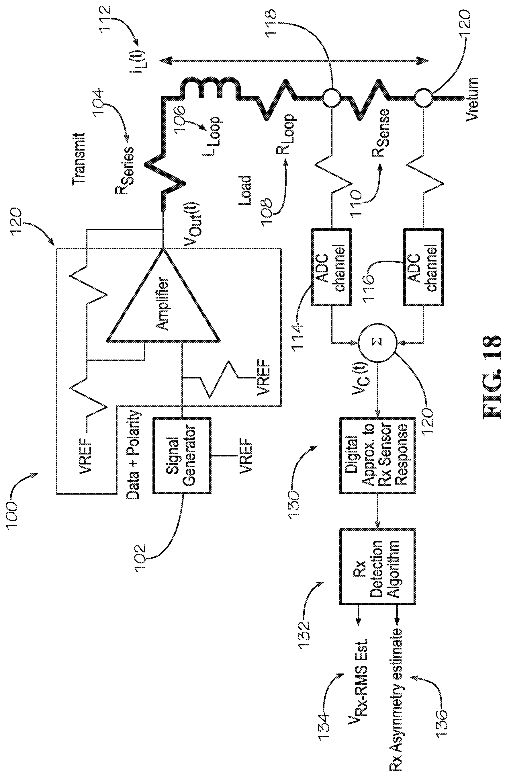
D00018
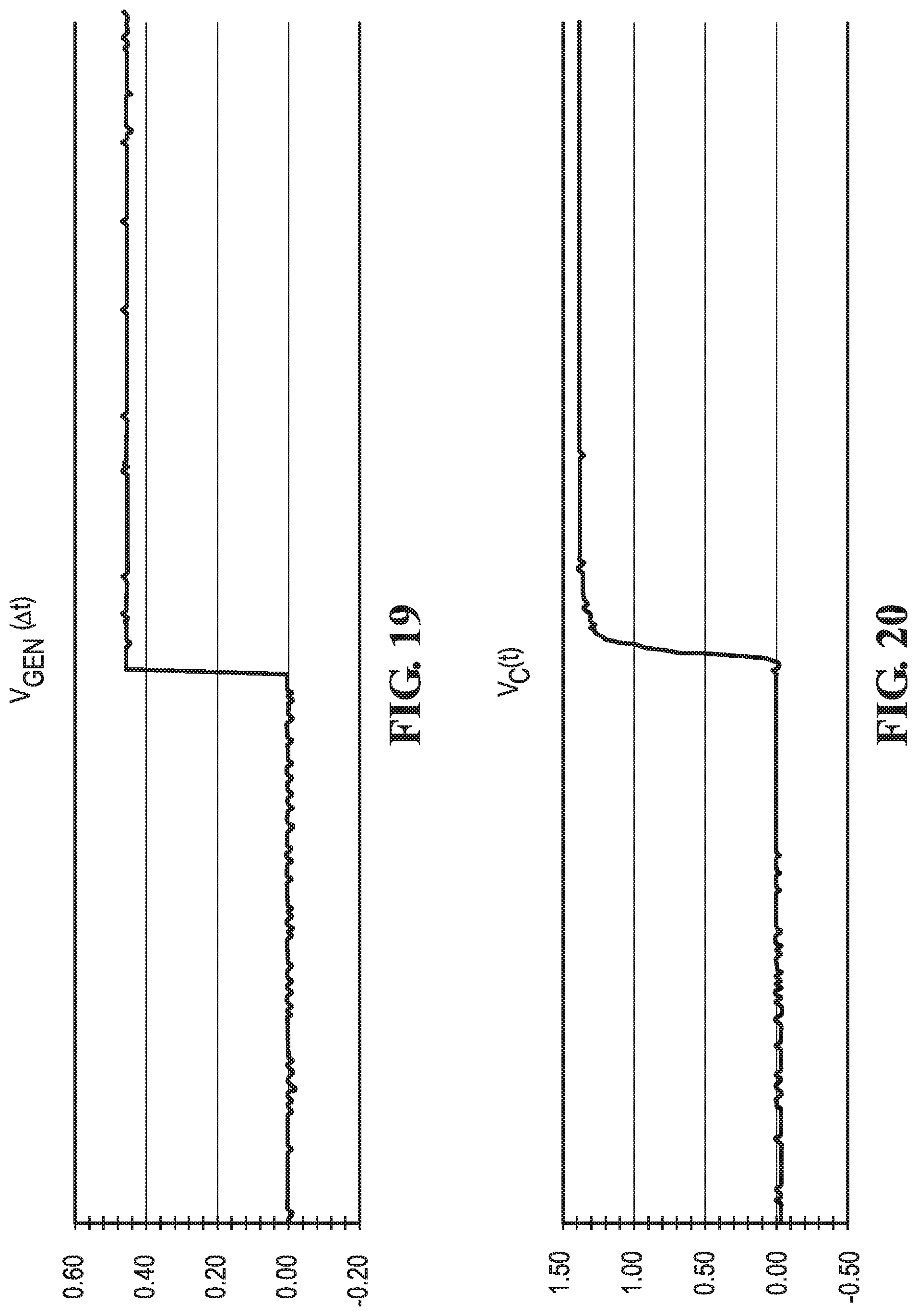
D00019

D00020

D00021

M00001

M00002
M00003

M00004

M00005

M00006

M00007
M00008

M00009

M00010

M00011
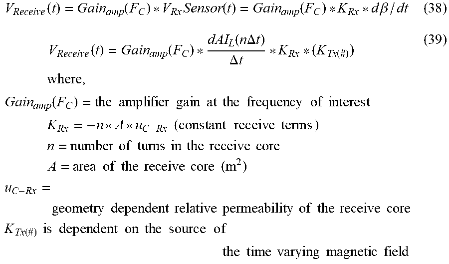
XML
uspto.report is an independent third-party trademark research tool that is not affiliated, endorsed, or sponsored by the United States Patent and Trademark Office (USPTO) or any other governmental organization. The information provided by uspto.report is based on publicly available data at the time of writing and is intended for informational purposes only.
While we strive to provide accurate and up-to-date information, we do not guarantee the accuracy, completeness, reliability, or suitability of the information displayed on this site. The use of this site is at your own risk. Any reliance you place on such information is therefore strictly at your own risk.
All official trademark data, including owner information, should be verified by visiting the official USPTO website at www.uspto.gov. This site is not intended to replace professional legal advice and should not be used as a substitute for consulting with a legal professional who is knowledgeable about trademark law.