Method and system for forming perforations
Bookbinder , et al.
U.S. patent number 10,611,667 [Application Number 15/325,636] was granted by the patent office on 2020-04-07 for method and system for forming perforations. This patent grant is currently assigned to Corning Incorporated. The grantee listed for this patent is Corning Incorporated. Invention is credited to Dana Craig Bookbinder, Stephan Lvovich Logunov, Albert Roth Nieber, Pushkar Tandon, Sergio Tsuda.


View All Diagrams
| United States Patent | 10,611,667 |
| Bookbinder , et al. | April 7, 2020 |
Method and system for forming perforations
Abstract
The embodiments disclosed herein relate to methods, systems, and system components for creating and arranging small (micron and smaller) defects or perforations in transparent materials in a particular manner, and, more particularly, to the arrangement of these defects, each of which has an average crack length, in a predetermined spaced-apart relation (each defect separated from an adjacent defect by a predetermined distance) defining a contour in a transparent material to lower the relative interface fracture toughness for subsequent planned induced separation.
| Inventors: | Bookbinder; Dana Craig (Corning, NY), Logunov; Stephan Lvovich (Corning, NY), Nieber; Albert Roth (Painted Post, NY), Tandon; Pushkar (Painted Post, NY), Tsuda; Sergio (Horseheads, NY) | ||||||||||
|---|---|---|---|---|---|---|---|---|---|---|---|
| Applicant: |
|
||||||||||
| Assignee: | Corning Incorporated (Corning,
NY) |
||||||||||
| Family ID: | 53776966 | ||||||||||
| Appl. No.: | 15/325,636 | ||||||||||
| Filed: | July 14, 2015 | ||||||||||
| PCT Filed: | July 14, 2015 | ||||||||||
| PCT No.: | PCT/US2015/040250 | ||||||||||
| 371(c)(1),(2),(4) Date: | January 11, 2017 | ||||||||||
| PCT Pub. No.: | WO2016/010949 | ||||||||||
| PCT Pub. Date: | January 21, 2016 |
Prior Publication Data
| Document Identifier | Publication Date | |
|---|---|---|
| US 20170158551 A1 | Jun 8, 2017 | |
Related U.S. Patent Documents
| Application Number | Filing Date | Patent Number | Issue Date | ||
|---|---|---|---|---|---|
| 62024070 | Jul 14, 2014 | ||||
| Current U.S. Class: | 1/1 |
| Current CPC Class: | B23K 26/50 (20151001); B23K 26/53 (20151001); B23K 26/0006 (20130101); C03B 33/0222 (20130101); B23K 2103/54 (20180801) |
| Current International Class: | C03B 33/02 (20060101); B23K 26/00 (20140101); B23K 26/50 (20140101); B23K 26/53 (20140101) |
References Cited [Referenced By]
U.S. Patent Documents
| 1790397 | January 1931 | Woods et al. |
| 2682134 | June 1954 | Stookey |
| 2749794 | June 1956 | O'Leary |
| 3647410 | March 1972 | Heaton et al. |
| 3695497 | October 1972 | Dear |
| 3695498 | October 1972 | Dear |
| 3729302 | April 1973 | Heaton |
| 3775084 | November 1973 | Heaton |
| 4226607 | October 1980 | Domken |
| 4441008 | April 1984 | Chan |
| 4546231 | October 1985 | Gresser et al. |
| 4646308 | February 1987 | Kafka et al. |
| 4764930 | August 1988 | Bille et al. |
| 4891054 | January 1990 | Bricker et al. |
| 4907586 | March 1990 | Bille et al. |
| 4918751 | April 1990 | Pessot et al. |
| 4929065 | May 1990 | Hagerty et al. |
| 5035918 | July 1991 | Vyas |
| 5040182 | August 1991 | Spinelli et al. |
| 5104210 | April 1992 | Tokas |
| 5108857 | April 1992 | Kitayama et al. |
| 5112722 | May 1992 | Tsujino et al. |
| 5114834 | May 1992 | Nachshon |
| 5265107 | November 1993 | Delfyett |
| 5400350 | March 1995 | Galvanauskas et al. |
| 5434875 | July 1995 | Rieger et al. |
| 5436925 | July 1995 | Lin et al. |
| 5553093 | September 1996 | Ramaswamy et al. |
| 5574597 | November 1996 | Kataoka et al. |
| 5586138 | December 1996 | Yokoyama |
| 5656186 | August 1997 | Mourou et al. |
| 5676866 | October 1997 | In Den Baumen et al. |
| 5684642 | November 1997 | Zumoto et al. |
| 5696782 | December 1997 | Harter et al. |
| 5736709 | April 1998 | Neiheisel |
| 5776220 | July 1998 | Allaire et al. |
| 6016223 | January 2000 | Suzuki et al. |
| 6016324 | January 2000 | Rieger et al. |
| 6033583 | March 2000 | Musket et al. |
| 6038055 | March 2000 | Hansch et al. |
| 6055829 | May 2000 | Witzmann et al. |
| 6078599 | June 2000 | Everage et al. |
| 6156030 | December 2000 | Neev |
| 6160835 | December 2000 | Kwon |
| 6186384 | February 2001 | Sawada |
| 6210401 | April 2001 | Lai |
| 6256328 | July 2001 | Delfyett et al. |
| 6259151 | July 2001 | Morrison |
| 6259512 | July 2001 | Mizouchi |
| 6272156 | August 2001 | Reed et al. |
| 6301932 | October 2001 | Allen et al. |
| 6322958 | November 2001 | Hayashi |
| 6339208 | January 2002 | Rockstroh et al. |
| 6373565 | April 2002 | Kafka et al. |
| 6381391 | April 2002 | Islam et al. |
| 6396856 | May 2002 | Sucha et al. |
| 6407360 | June 2002 | Choo et al. |
| 6438996 | August 2002 | Cuvelier |
| 6445491 | September 2002 | Sucha et al. |
| 6449301 | September 2002 | Wu et al. |
| 6484052 | November 2002 | Visuri et al. |
| 6489589 | December 2002 | Alexander |
| 6501578 | December 2002 | Bernstein et al. |
| 6552301 | April 2003 | Herman et al. |
| 6573026 | June 2003 | Aitken et al. |
| 6592703 | July 2003 | Habeck et al. |
| 6635849 | October 2003 | Okawa et al. |
| 6635850 | October 2003 | Amako et al. |
| 6720519 | April 2004 | Liu et al. |
| 6729161 | May 2004 | Miura et al. |
| 6744009 | June 2004 | Xuan et al. |
| 6787732 | September 2004 | Xuan et al. |
| 6800237 | October 2004 | Yamamoto et al. |
| 6800831 | October 2004 | Hoetzel |
| 6958094 | October 2005 | Ohmi et al. |
| 6992026 | January 2006 | Fukuyo et al. |
| 7009138 | March 2006 | Amako et al. |
| 7353829 | April 2008 | Wachter et al. |
| 7402773 | July 2008 | Nomaru |
| 7511886 | March 2009 | Schultz et al. |
| 7535634 | May 2009 | Savchenkov et al. |
| 7633033 | December 2009 | Thomas et al. |
| 7642483 | January 2010 | You et al. |
| 7649153 | January 2010 | Haight et al. |
| 7726532 | June 2010 | Gonoe |
| 8104385 | January 2012 | Hayashi et al. |
| 8118971 | February 2012 | Hori et al. |
| 8132427 | March 2012 | Brown et al. |
| 8168514 | May 2012 | Garner et al. |
| 8245539 | August 2012 | Lu et al. |
| 8245540 | August 2012 | Abramov et al. |
| 8269138 | September 2012 | Garner et al. |
| 8283595 | October 2012 | Fukuyo et al. |
| 8292141 | October 2012 | Cox et al. |
| 8296066 | October 2012 | Zhao et al. |
| 8327666 | December 2012 | Harvey et al. |
| 8341976 | January 2013 | Dejneka et al. |
| 8347651 | January 2013 | Abramov et al. |
| 8358888 | January 2013 | Ramachandran |
| 8444906 | May 2013 | Lee et al. |
| 8448471 | May 2013 | Kumatani et al. |
| 8518280 | August 2013 | Hsu et al. |
| 8549881 | October 2013 | Brown et al. |
| 8584354 | November 2013 | Cornejo et al. |
| 8584490 | November 2013 | Garner et al. |
| 8592716 | November 2013 | Abramov et al. |
| 8604380 | December 2013 | Howerton et al. |
| 8607590 | December 2013 | Glaesemann et al. |
| 8616024 | December 2013 | Cornejo et al. |
| 8635887 | January 2014 | Black et al. |
| 8680489 | March 2014 | Martinez et al. |
| 8685838 | April 2014 | Fukuyo et al. |
| 8697228 | April 2014 | Carre et al. |
| 8720228 | May 2014 | Li |
| 8826696 | September 2014 | Brown et al. |
| 8852698 | October 2014 | Fukumitsu |
| 8887529 | November 2014 | Lu et al. |
| 8916798 | December 2014 | Pluss et al. |
| 8943855 | February 2015 | Gomez et al. |
| 8971053 | March 2015 | Kariya et al. |
| 9138913 | September 2015 | Arai et al. |
| 9227868 | January 2016 | Matsumoto et al. |
| 9290407 | March 2016 | Barefoot et al. |
| 9296066 | March 2016 | Hosseini et al. |
| 9324791 | April 2016 | Tamemoto |
| 9327381 | May 2016 | Lee et al. |
| 9446590 | September 2016 | Chen et al. |
| 9481598 | November 2016 | Bergh et al. |
| 2002/0046997 | April 2002 | Nam et al. |
| 2002/0082466 | June 2002 | Han |
| 2002/0097486 | July 2002 | Yamaguchi et al. |
| 2002/0110639 | August 2002 | Bruns |
| 2003/0006221 | January 2003 | Hong et al. |
| 2003/0007773 | January 2003 | Kondo et al. |
| 2004/0221615 | November 2004 | Postupack et al. |
| 2005/0024743 | February 2005 | Camy-Peyret |
| 2005/0098548 | May 2005 | Kobayashi et al. |
| 2005/0115938 | June 2005 | Sawaki et al. |
| 2005/0274702 | December 2005 | Deshi |
| 2005/0277270 | December 2005 | Yoshikawa et al. |
| 2006/0011593 | January 2006 | Fukuyo |
| 2006/0028728 | February 2006 | Li |
| 2006/0109874 | May 2006 | Shiozaki et al. |
| 2006/0127679 | June 2006 | Gulati et al. |
| 2006/0227440 | October 2006 | Gluckstad |
| 2006/0266744 | November 2006 | Nomaru |
| 2006/0289410 | December 2006 | Morita et al. |
| 2007/0091977 | April 2007 | Sohn et al. |
| 2007/0111390 | May 2007 | Komura et al. |
| 2007/0111480 | May 2007 | Maruyama et al. |
| 2007/0119831 | May 2007 | Kandt |
| 2007/0132977 | June 2007 | Komatsuda |
| 2007/0138151 | June 2007 | Tanaka et al. |
| 2007/0177116 | August 2007 | Amako |
| 2007/0202619 | August 2007 | Tamura et al. |
| 2007/0298529 | December 2007 | Maeda et al. |
| 2008/0000884 | January 2008 | Sugiura et al. |
| 2008/0079940 | April 2008 | Sezerman et al. |
| 2008/0099444 | May 2008 | Misawa et al. |
| 2009/0013724 | January 2009 | Koyo et al. |
| 2009/0176034 | July 2009 | Ruuttu et al. |
| 2009/0183764 | July 2009 | Meyer |
| 2009/0242528 | October 2009 | Howerton et al. |
| 2009/0250446 | October 2009 | Sakamoto |
| 2009/0294419 | December 2009 | Abramov et al. |
| 2009/0294422 | December 2009 | Lubatschowski et al. |
| 2009/0324899 | December 2009 | Feinstein et al. |
| 2010/0025387 | February 2010 | Arai et al. |
| 2010/0029460 | February 2010 | Shojiya et al. |
| 2010/0032087 | February 2010 | Takahashi et al. |
| 2010/0086741 | April 2010 | Bovatsek et al. |
| 2010/0089631 | April 2010 | Sakaguchi et al. |
| 2010/0089882 | April 2010 | Tamura |
| 2010/0102042 | April 2010 | Garner et al. |
| 2010/0129603 | May 2010 | Blick et al. |
| 2010/0147813 | June 2010 | Lei et al. |
| 2010/0252540 | October 2010 | Lei et al. |
| 2010/0252959 | October 2010 | Lei et al. |
| 2010/0276505 | November 2010 | Smith |
| 2010/0279067 | November 2010 | Sabia et al. |
| 2010/0287991 | November 2010 | Brown et al. |
| 2010/0326138 | December 2010 | Kumatani et al. |
| 2011/0049764 | March 2011 | Lee et al. |
| 2011/0049765 | March 2011 | Li et al. |
| 2011/0088324 | April 2011 | Wessel |
| 2011/0100401 | May 2011 | Fiorentini |
| 2011/0132881 | June 2011 | Liu |
| 2011/0139760 | June 2011 | Shah et al. |
| 2011/0183116 | July 2011 | Hung et al. |
| 2011/0210105 | September 2011 | Romashko et al. |
| 2011/0240611 | October 2011 | Sandstrom et al. |
| 2011/0277507 | November 2011 | Lu et al. |
| 2011/0318555 | December 2011 | Bookbinder et al. |
| 2012/0017642 | January 2012 | Teranishi et al. |
| 2012/0047951 | March 2012 | Dannoux et al. |
| 2012/0048604 | March 2012 | Cornejo et al. |
| 2012/0061440 | March 2012 | Roell |
| 2012/0064306 | March 2012 | Kang et al. |
| 2012/0067858 | March 2012 | Kangastupa et al. |
| 2012/0103018 | May 2012 | Lu et al. |
| 2012/0131962 | May 2012 | Mitsugi et al. |
| 2012/0135195 | May 2012 | Glaesemann et al. |
| 2012/0135607 | May 2012 | Shimoi et al. |
| 2012/0135608 | May 2012 | Shimoi et al. |
| 2012/0145331 | June 2012 | Gomez et al. |
| 2012/0196071 | August 2012 | Cornejo et al. |
| 2012/0234049 | September 2012 | Bolton |
| 2012/0234807 | September 2012 | Sercel et al. |
| 2012/0237731 | September 2012 | Boegli |
| 2012/0255935 | October 2012 | Kakui et al. |
| 2012/0299219 | November 2012 | Shimoi et al. |
| 2012/0302139 | November 2012 | Darcangelo et al. |
| 2013/0019637 | January 2013 | Sol et al. |
| 2013/0034688 | February 2013 | Koike et al. |
| 2013/0044371 | February 2013 | Rupp et al. |
| 2013/0056450 | March 2013 | Lissotschenko et al. |
| 2013/0061636 | March 2013 | Imai et al. |
| 2013/0068736 | March 2013 | Mielke et al. |
| 2013/0075480 | March 2013 | Yokogi et al. |
| 2013/0091897 | April 2013 | Fugii et al. |
| 2013/0122264 | May 2013 | Fujii et al. |
| 2013/0126573 | May 2013 | Hosseini et al. |
| 2013/0129947 | May 2013 | Harvey et al. |
| 2013/0133367 | May 2013 | Abramov et al. |
| 2013/0143416 | June 2013 | Norval |
| 2013/0149434 | June 2013 | Oh et al. |
| 2013/0149494 | June 2013 | Koike et al. |
| 2013/0167590 | July 2013 | Teranishi et al. |
| 2013/0174607 | July 2013 | Wootton et al. |
| 2013/0174610 | July 2013 | Teranishi et al. |
| 2013/0180285 | July 2013 | Kariya |
| 2013/0189806 | July 2013 | Hoshino |
| 2013/0192305 | August 2013 | Black et al. |
| 2013/0209731 | August 2013 | Nattermann et al. |
| 2013/0220982 | August 2013 | Thomas et al. |
| 2013/0221053 | August 2013 | Zhang |
| 2013/0224439 | August 2013 | Zhang et al. |
| 2013/0228918 | September 2013 | Chen et al. |
| 2013/0247615 | September 2013 | Boek et al. |
| 2013/0266757 | October 2013 | Giron et al. |
| 2013/0270240 | October 2013 | Kondo |
| 2013/0280495 | October 2013 | Matsumoto |
| 2013/0288010 | October 2013 | Akarapu et al. |
| 2013/0291598 | November 2013 | Saito et al. |
| 2013/0312460 | November 2013 | Kunishi et al. |
| 2013/0323469 | December 2013 | Abramov et al. |
| 2013/0334185 | December 2013 | Nomaru |
| 2013/0340480 | December 2013 | Nattermann et al. |
| 2014/0027951 | January 2014 | Srinivas et al. |
| 2014/0034730 | February 2014 | Lee |
| 2014/0042202 | February 2014 | Lee |
| 2014/0047957 | February 2014 | Wu |
| 2014/0102146 | April 2014 | Saito et al. |
| 2014/0110040 | April 2014 | Cok |
| 2014/0113797 | April 2014 | Yamada et al. |
| 2014/0133119 | May 2014 | Kariya et al. |
| 2014/0141217 | May 2014 | Gulati et al. |
| 2014/0147623 | May 2014 | Shorey et al. |
| 2014/0147624 | May 2014 | Streltsov et al. |
| 2014/0165652 | June 2014 | Saito |
| 2014/0174131 | June 2014 | Saito et al. |
| 2014/0199519 | July 2014 | Schillinger et al. |
| 2014/0216108 | August 2014 | Wiegel et al. |
| 2014/0290310 | October 2014 | Green |
| 2014/0320947 | October 2014 | Egerton et al. |
| 2014/0333929 | November 2014 | Sung et al. |
| 2014/0361463 | December 2014 | DeSimone et al. |
| 2015/0034612 | February 2015 | Hosseini et al. |
| 2015/0038313 | February 2015 | Hosseini |
| 2015/0075221 | March 2015 | Kawaguchi et al. |
| 2015/0075222 | March 2015 | Mader |
| 2015/0110442 | April 2015 | Zimmel et al. |
| 2015/0118522 | April 2015 | Hosseini |
| 2015/0136743 | May 2015 | Hosseini |
| 2015/0140241 | May 2015 | Hosseini |
| 2015/0140735 | May 2015 | Hosseini |
| 2015/0151380 | June 2015 | Hosseini |
| 2015/0158120 | June 2015 | Courvoisier et al. |
| 2015/0165548 | June 2015 | Marjanovic et al. |
| 2015/0165560 | June 2015 | Hackert et al. |
| 2015/0165562 | June 2015 | Marjanovic et al. |
| 2015/0165563 | June 2015 | Manley et al. |
| 2015/0166391 | June 2015 | Marjanovic et al. |
| 2015/0166393 | June 2015 | Marjanovic et al. |
| 2015/0166394 | June 2015 | Marjanovic et al. |
| 2015/0166395 | June 2015 | Marjanovic et al. |
| 2015/0166396 | June 2015 | Marjanovic et al. |
| 2015/0166397 | June 2015 | Marjanovic et al. |
| 2015/0183679 | July 2015 | Saito |
| 2015/0232369 | August 2015 | Marjanovic et al. |
| 2015/0299018 | October 2015 | Bhuyan et al. |
| 2015/0311058 | October 2015 | Antsiferov |
| 2015/0360991 | December 2015 | Grundmueller et al. |
| 2015/0367442 | December 2015 | Bovatsek et al. |
| 2016/0008927 | January 2016 | Grundmueller et al. |
| 2016/0009066 | January 2016 | Nieber et al. |
| 2016/0023922 | January 2016 | Addiego et al. |
| 2016/0031745 | February 2016 | Ortner et al. |
| 2016/0060156 | March 2016 | Krueger et al. |
| 2016/0279895 | September 2016 | Marjanovic et al. |
| 2016/0280580 | September 2016 | Bohme |
| 2016/0290791 | October 2016 | Buono et al. |
| 2017/0052381 | February 2017 | Huang et al. |
| 2017/0169847 | June 2017 | Tamaki |
| 2017/0368638 | December 2017 | Tayebati et al. |
| 2388062 | Jul 2000 | CN | |||
| 1283409 | Nov 2006 | CN | |||
| 101386466 | Mar 2009 | CN | |||
| 101502914 | Aug 2009 | CN | |||
| 201357287 | Dec 2009 | CN | |||
| 101637849 | Feb 2010 | CN | |||
| 201471092 | May 2010 | CN | |||
| 102672355 | Sep 2012 | CN | |||
| 102898014 | Jan 2013 | CN | |||
| 102923939 | Feb 2013 | CN | |||
| 103013374 | Apr 2013 | CN | |||
| 103143841 | Jun 2013 | CN | |||
| 203021443 | Jun 2013 | CN | |||
| 103273195 | Sep 2013 | CN | |||
| 103316990 | Sep 2013 | CN | |||
| 103359947 | Oct 2013 | CN | |||
| 103359948 | Oct 2013 | CN | |||
| 103531414 | Jan 2014 | CN | |||
| 103746027 | Apr 2014 | CN | |||
| 203509350 | Apr 2014 | CN | |||
| 104344202 | Feb 2015 | CN | |||
| 2231330 | Oct 1974 | DE | |||
| 102006035555 | Jan 2008 | DE | |||
| 102012010635 | Nov 2013 | DE | |||
| 102012110971 | May 2014 | DE | |||
| 102013223637 | May 2015 | DE | |||
| 270897 | Feb 1992 | EP | |||
| 609978 | Aug 1994 | EP | |||
| 656241 | Dec 1998 | EP | |||
| 938946 | Sep 1999 | EP | |||
| 949541 | Oct 1999 | EP | |||
| 1159104 | Aug 2004 | EP | |||
| 1609559 | Dec 2005 | EP | |||
| 1043110 | Aug 2006 | EP | |||
| 2133170 | Dec 2009 | EP | |||
| 2202545 | Jun 2010 | EP | |||
| 2574983 | Apr 2013 | EP | |||
| 2754524 | Jul 2014 | EP | |||
| 2781296 | Sep 2014 | EP | |||
| 2783784 | Oct 2014 | EP | |||
| 2859984 | Apr 2015 | EP | |||
| 2989294 | Oct 2013 | FR | |||
| 1242172 | Aug 1971 | GB | |||
| 2481190 | Jan 2015 | GB | |||
| 1179770 | Jul 1989 | JP | |||
| 6318756 | Nov 1994 | JP | |||
| 9109243 | Apr 1997 | JP | |||
| 11197498 | Jul 1999 | JP | |||
| 11269683 | Oct 1999 | JP | |||
| 11330597 | Nov 1999 | JP | |||
| 11347758 | Dec 1999 | JP | |||
| 2001138083 | May 2001 | JP | |||
| 2002210730 | Jul 2002 | JP | |||
| 2002228818 | Aug 2002 | JP | |||
| 2003025085 | Jan 2003 | JP | |||
| 2003062756 | Mar 2003 | JP | |||
| 2003114400 | Apr 2003 | JP | |||
| 2003154517 | May 2003 | JP | |||
| 2003181668 | Jul 2003 | JP | |||
| 2003238178 | Aug 2003 | JP | |||
| 2004209675 | Jul 2004 | JP | |||
| 2005104819 | Apr 2005 | JP | |||
| 2005205440 | Aug 2005 | JP | |||
| 2005288503 | Oct 2005 | JP | |||
| 3775250 | May 2006 | JP | |||
| 3775410 | May 2006 | JP | |||
| 2006130691 | May 2006 | JP | |||
| 2006248885 | Sep 2006 | JP | |||
| 2007021548 | Feb 2007 | JP | |||
| 2007196277 | Aug 2007 | JP | |||
| 2007253203 | Oct 2007 | JP | |||
| 2009172633 | Aug 2009 | JP | |||
| 2010017990 | Jan 2010 | JP | |||
| 2010046761 | Mar 2010 | JP | |||
| 4592855 | Dec 2010 | JP | |||
| 2011049398 | Mar 2011 | JP | |||
| 4672689 | Apr 2011 | JP | |||
| 2011517299 | Jun 2011 | JP | |||
| 4880820 | Feb 2012 | JP | |||
| 2012024782 | Feb 2012 | JP | |||
| 2012031018 | Feb 2012 | JP | |||
| 2012159749 | Aug 2012 | JP | |||
| 2012187618 | Oct 2012 | JP | |||
| 2013007842 | Jan 2013 | JP | |||
| 2013031879 | Feb 2013 | JP | |||
| 2013043808 | Mar 2013 | JP | |||
| 2013075802 | Apr 2013 | JP | |||
| 2013091578 | May 2013 | JP | |||
| 5274085 | Aug 2013 | JP | |||
| 5300544 | Sep 2013 | JP | |||
| 2013187247 | Sep 2013 | JP | |||
| 2013203630 | Oct 2013 | JP | |||
| 2013203631 | Oct 2013 | JP | |||
| 2013223886 | Oct 2013 | JP | |||
| 2012015366 | Feb 2002 | KR | |||
| 2009057161 | Jun 2009 | KR | |||
| 1020621 | Mar 2011 | KR | |||
| 1120471 | Mar 2012 | KR | |||
| 2012074508 | Jul 2012 | KR | |||
| 2013031380 | Mar 2013 | KR | |||
| 1269474 | May 2013 | KR | |||
| 2013124646 | Nov 2013 | KR | |||
| 1344368 | Dec 2013 | KR | |||
| 2014022980 | Feb 2014 | KR | |||
| 2014022981 | Feb 2014 | KR | |||
| 2014064220 | May 2014 | KR | |||
| 201139025 | Nov 2011 | TW | |||
| 201226345 | Jul 2012 | TW | |||
| 1999029243 | Jun 1999 | WO | |||
| 1999063900 | Dec 1999 | WO | |||
| 2004110693 | Dec 2004 | WO | |||
| 2006073098 | Jul 2006 | WO | |||
| 2007094160 | Aug 2007 | WO | |||
| 2008049389 | May 2008 | WO | |||
| 2008080182 | Jul 2008 | WO | |||
| 2008128612 | Oct 2008 | WO | |||
| 2009114375 | Sep 2009 | WO | |||
| 2010035736 | Apr 2010 | WO | |||
| 2010111609 | Sep 2010 | WO | |||
| 2010129459 | Nov 2010 | WO | |||
| 2011025908 | Mar 2011 | WO | |||
| 2011056781 | May 2011 | WO | |||
| 2012006736 | Jan 2012 | WO | |||
| 2012075072 | Jun 2012 | WO | |||
| 2012108052 | Aug 2012 | WO | |||
| 2012166753 | Dec 2012 | WO | |||
| 2013022148 | Feb 2013 | WO | |||
| 2013043173 | Mar 2013 | WO | |||
| 2013138802 | Sep 2013 | WO | |||
| 2013150990 | Oct 2013 | WO | |||
| 2013153195 | Oct 2013 | WO | |||
| 2014028022 | Feb 2014 | WO | |||
| 2014064492 | May 2014 | WO | |||
| 2014079478 | May 2014 | WO | |||
| 2014079570 | May 2014 | WO | |||
| 2014085663 | Jun 2014 | WO | |||
| 2014111385 | Jul 2014 | WO | |||
| 2014111794 | Jul 2014 | WO | |||
| 2014161534 | Oct 2014 | WO | |||
| 2014161535 | Oct 2014 | WO | |||
| 2015077113 | May 2015 | WO | |||
| 2015095088 | Jun 2015 | WO | |||
| 2015095090 | Jun 2015 | WO | |||
| 2015095146 | Jun 2015 | WO | |||
| 2015127583 | Sep 2015 | WO | |||
| 2016005455 | Jan 2016 | WO | |||
| 2016010954 | Jan 2016 | WO | |||
| 20160154284 | Sep 2016 | WO | |||
Other References
|
Arimoto, R. et al.; Imaging properties of axicon in a scanning optical system; Applied Optics; Nov. 1, 1991; pp. 6653-6657; vol. 31, No. 31; Optical Society of America. cited by applicant . Betriebsanleitung; TruMicro 5000; Aug. 2011; pp. 1-4. cited by applicant . Bhuyan, M. et al.; High aspect ratio nanochannel machining using single shot femtosecond Bessel beams; Applied Physics Letters; Aug. 23, 2010; pp. 081102-1-081102-3; vol. 97. cited by applicant . Bhuyan, M. et al.; High aspect ratio taper-free microchannel fabrication using femtosecond Bessel beams; Optics Express; Jan. 18, 2010; pp. 566-574; vol. 18, No. 2; Optical Society of America. cited by applicant . Cubeddu, R. et al.; A compact time-resolved reflectance system for dual-wavelength multichannel assessment of tissue absorption and scattering; SPIE Conference on Optical Tomography and Spectroscopy of Tissue III; San Jose, Califomia; Jan. 1999; pp. 450-455; vol. 3597; SPIE. cited by applicant . Cubeddu, R. et al.; Compact tissue oximeter based on dual-wavelength multichannel time-resolved reflectance; Applied Optics; Jun. 1, 1999; pp. 3670-3680; vol. 38, No. 16; Optical Society of America. cited by applicant . Ding, Z. et al.; High-resolution optical coherence tomography over a large depth range with an axicon lens; Optics Letters; Feb. 15, 2002; pp. 243-245; vol. 27, No. 4; Optical Society of America. cited by applicant . EagleEtch; TheAnti-glare Glass for Technical Display Applications; Glass and Polymer Technologies; pp. 1-8; EuropTec USA Inc. cited by applicant . Girkin, J. et al.; Macroscopic multiphoton biomedical imaging using semiconductor saturable Bragg reflector modelocked Lasers; SPIE Conference on Commercial and Biomedical Applications of Ultrafast Lasers; San Jose, California; Jan. 1999; pp. 92-98; vol. 3616; SPIE. cited by applicant . Glezer, E. et al.; Ultrafast-laser driven micro-explosions in transparent materials; Applied Physics Letters; 1997; pp. 882-884, vol. 71. cited by applicant . Golub, I.; Fresnel axicon; Optics Letters; Jun. 15, 2006; pp. 1890-1892;. vol. 31, No. 12; Optical Society of America. cited by applicant . Herman, P. et al.; Laser micromachining of `transparent` fused silica with 1-ps pulses and pulse trains; SPIE Conference on Commercial and Biomedical Applications of Ultrafast Lasers; San Jose, California; Jan. 1999; pp. 148-155; vol. 3616; SPIE. cited by applicant . Kosareva, O. et al.; Formation of extended plasma channels in a condensed medium upon axicon focusing of a femtosecond laser pulse; Quantum Electronics; 2005; pp. 1013-1014; vol. 35, No. 11; Kvantovaya Elektronika and Turpion Ltd. cited by applicant . Kruger, J. et al.; Femtosecond-pulse visible laser processing of transparent materials; Applied Surface Science; 1996; pp. 430-438; Elsevier B.V. cited by applicant . Kruger, J. et al.; Laser micromachining of barium aluminium borosilicate glass with pulse durations between 20 fs and 3 ps; Applied Surface Science; 1998; pp. 892-898; Elsevier B.V. cited by applicant . Kruger, J. et al.; Structuring of dielectric and metallic materials with ultrashort laser pulses between 20 fs and 3 ps; SPIE Proceedings; San Jose, California; Feb. 8, 1997; pp. 40-47 vol. 2991; SPIE. cited by applicant . Lapczyna, M. et al.; Ultra high repetition rate (133 MHz) laser ablation of aluminum with 1.2-ps pulses; Applied Physics A Materials Science & Processing; Dec. 28, 1999; pp. S883-S886; vol. 69 (Suppl).; Springer-Verlag. cited by applicant . Perry, M. et al.; Ultrashort-Pulse Laser Machining; Lawrence Livermore National Laboratory; Sep. 1998; pp. i-30. cited by applicant . Perry, M. et al.; Ultrashort-Pulse Laser Machining; International Congress on Applications of Lasers and Electro-Optics; Orlando, Florida; Nov. 16-19, 1998; pp. 1-24. cited by applicant . Perry, M. et al.; Ultrashort-pulse laser machining of dielectric materials; Journal of Applied Physics; May 1, 1999; pp. 6803-6810; vol. 85, No. 9; American Institute of Physics. cited by applicant . PHAROS High-power Femtosecond Laser System specification; Light Conversion; 2011; pp. 1-2. cited by applicant . Polynkin, P. et al.; Extended filamentation with temporally chirped femtosecond Bessel-Gauss beams in air; Optics Express; Jan. 19, 2009; pp. 575-584; vol. 17, No. 2; Optical Society of America. cited by applicant . Serafetinides, A. et al.; Ultra-short pulsed laser ablation of polymers; Applied Surface Science; 2011; pp. 42-56; vol. 180; Elsevier Science B.V. cited by applicant . Sundaram, S. et al.; Inducing and probing non-thermal transitions in semiconductors using femtosecond laser pulses; Nature Materials; Dec. 2002; pp. 217-224; vol. 1; Nature Publishing Group. cited by applicant . Vanagas, E. et al.; Glass cutting by femtosecond pulsed irradiation; Journal of Micro/Nanolithography, MEMS, and MOEMS; Mar. 31, 2004; pp. 1-18; vol. 3, Issue 2; SPIE. cited by applicant . Varel, H. et al.; Micromachining of quartz with ultrashort laser pulses; Applied Physics A Materials Science & Processing; 1997; pp. 367-373; vol. 65. cited by applicant . Yoshino, F. et al.; Micromachining with a High Repetition Rate Femtosecond Fiber Laser; JLMN-Journal of Laser Micro/Nanoengineering; 2008; pp. 157-162; vol. 3, No. 3. cited by applicant . Zeng, D. et al.; Characteristic analysis of refractive axicon system for optical trepanning; Optical Engineering; Sep. 2006; pp. 094302-1-094302-10; vol. 45, No. 9. cited by applicant . Zhang, G. et al.; Design of diffractive-phase axicon illuminated by a Gaussian-profile beam; Acta Physica Sinica; May 1996; pp. 354-364; vol. 5, No. 5; Chin. Phys. Soc. cited by applicant . Kerr. "Filamentary tracks formed in transparent optical glass by laser beam self-focusing. II. Theoretical Analysis" Physical Review A. 4(3) 1971, pp. 1196-1218. cited by applicant . Abakians, H. et al.; Evaporative Cutting of a Semitransparent Body With a Moving CW Laser; Journal of Heat Transfer; Nov. 1988; pp. 924-930; vol. 110; ASME. cited by applicant . Ahmed, F. et al.; Display glass cutting by femtosecond laser induced single shot periodic void array; Applied Physics A Material Science & Processing; Jun. 3, 2008; pp. 189-192; vol. 93; Springer-Verlag. cited by applicant . Bagchi, S. et al.; Fast ion beams from intense, femtosecond laser irradiated nanostructured surfaces; Applied Physics B Lasers and Optics; Jun. 27, 2007; pp. 167-173; vol. 88; Springer-Verlag. cited by applicant . Bhuyan, M.K. et al.; Femtosecond non-diffracting Bessel beams and controlled nanoscale ablation; ResearchGate Conference Paper; Sep. 2011; pp. 1-4. cited by applicant . Bhuyan, M.K. et al.; Laser micro- and nanostructuring using femtosecond Bessel beams; The European Physical Journal Special Topics; Dec. 7, 2011; pp. 101-110; vol. 1999; EDP Sciences, Springer-Verlag. cited by applicant . Bhuyan, M.K. et al.; Single-shot high aspect ratio bulk nanostructuring of fused silica using chirp-controlled ultrafast laser Bessel beams; Applied Physics Letters; Jan. 14, 2014; pp. 021107-1-021107-4; vol. 104; AIP Publishing LLC. cited by applicant . Bhuyam, M.K. et al.; Ultrafast Bessel beams for high aspect ratio taper free micromachining of glass; Nonlinear Optics and Applications IV; 2010; pp. 77281V-1-77281V-8; vol. 7728; SPIE. cited by applicant . Case Design Guidelines for Apple Devices; Sep. 13, 2013; pp. 1-58; Apple Inc. cited by applicant . Chiao, R. Y. et al.; Self-Trapping of Optical Beams; Physical Review Letters; Oct. 12, 1964; pp. 479-482; vol. 13, No. 15. cited by applicant . Corning Eagle AMLCD Glass Substrates Material Information; Apr. 2005; pp. MIE 201-1-MIE 201-3; Corning Incorporated. cited by applicant . Corning 1737 AMLCD Glass Substrates Material Information; Aug. 2002; pp. MIE 101-1-MIE 101-3; Corning Incorporated. cited by applicant . Couairon, A. et al.; Femtosecond filamentation in transparent media; ScienceDirect Physical Reports; Feb. 6, 2007; pp. 47-189; vol. 441; Elsevier B.V. cited by applicant . Courvoisier, F. et al.; Applications of femtosecond Bessel beams to laser ablation; Applied Physics A Materials Science & Processing; Sep. 6, 2012; pp. 29-34; vol. 112; Springer-Verlag. cited by applicant . Courvoisier, F. et al.; Surface nanoprocessing with nondiffracting femtosecond Bessel beams; Optics Letters; Oct. 15, 2009; pp. 3163-3165; vol. 34, No. 20; Optical Society of America. cited by applicant . Dong, M. et al.; On-axis irradiance distribution of axicons illuminated by spherical wave; ScienceDirect Optics & Laser Technology; Sep. 2007; pp. 1258-1261; vol. 39; Elsevier Ltd. cited by applicant . Duocastella, M. et al.; Bessel and annular beams for materials processing; Laser & Photonics Reviews; 2012; pp. 607-621; vol. 6, No. 5. cited by applicant . Durnin, J.; Exact solutions for nondiffracting beams. I. The scalar theory; J. Opt. Soc. Am. A; Apr. 1987; pp. 651-654; vol. 4, No. 4; Optical Society of America. cited by applicant . Eaton, S. et al.; Heat accumulation effects in femtosecond laser-written waveguides with variable repetition rate; Optics Express; Jun. 13, 2005; pp. 4708-4716; vol. 13, No. 12; Optical Society of America. cited by applicant . Gattass, R. et al.; Micromachining of bulk glass with bursts of femtosecond laser pulses at variable repetition rates; Optics Express; Jun. 12, 2006; pp. 5279-5284; vol. 14, No. 12; Optical Society of America. cited by applicant . Gori, F. et al.; Analytical derivation of the optimum triplicator; Optics Communications; Dec. 1, 1998; pp. 13-16; vol. 157; Elsevier B.V. cited by applicant . Honda, M. et al.; A Novel Polymer Film that Controls Light Transmission; Progress in Pacific Polymer Science 3; 1994; pp. 159-169; Springer-Verlag Berlin Heidelberg. cited by applicant . Hu, Z. et al.; 5-Axis Laser Cutting Interference Detection and Correction Based on STL Model; Chinese Journal of Lasers; Dec. 2009; pp. 3313-3317; vol. 36, No. 12. cited by applicant . Huang, Z. et al.; Laser etching of glass substrates by 1064 nm laser irradiation; Applied Physics A Materials Science & Processing; Jun. 6, 2008; pp. 159-163; vol. 93; Springer-Verlag. cited by applicant . Juodkazis, S. et al.; Laser-Induced Microexplosion Confined in the Bulk of a Sapphire Crystal: Evidence of Multimegabar Pressures; Physical Review Letters; Apr. 28, 2006; pp. 166101-1-166101-4; vol. 96; The American Physical Society. cited by applicant . Karlsson, S. et al.; The Technology of Chemical Glass Strengthening--A Review; Glass Technology--European Journal of Glass Science and Technology Part A; Apr. 2010; pp. 41-54; vol. 51, No. 2. cited by applicant . Levy, U. et al.; Design, fabrication, and characterization of circular Dammann gratings based on grayscale lithography; Optics Letters; Mar. 15, 2010; pp. 880-882; vol. 35, No. 6; Optical Society of America. cited by applicant . Liu, X. et al.; Laser Ablation and Micromachining with Ultrashort Laser Pulses; IEEE Journal of Quantum Electronics; Oct. 1997; p. 1706-1716; vol. 33, No. 10; IEEE. cited by applicant . Maeda, K. et al.; Optical performance of angle dependent light control glass; Optical Materials Technology for Energy Efficiency and Solar Energy Conversion X; 1991; pp. 138-148; vol. 1536; SPIE. cited by applicant . Mbise, G. et al.; Angular selective window coatings; theory and experiments; J. Phys. D: Appl. Phys.; 1997; pp. 2103-2122; vol. 30; IOP Publishing Ltd. cited by applicant . McGloin, D. et al.; Bessel beams: diffraction in a new light; Contemporary Physics; Jan.-Feb. 2005; pp. 15-28; vol. 46; Taylor & Francis Ltd. cited by applicant . Merola, F. et al.; Characterization of Bessel beams generated by polymeric microaxicons; Measurement Science and Technology; May 15, 2012; pp. 1-10; vol. 23; IOP Publishing Ltd. cited by applicant . Mirkhalaf, M. et al.; Overcoming the brittleness of glass through bio-inspiration and micro-architecture; Nature Communications; Jan. 28, 2014; pp. 1-9; Macmillan Publishers Limited. cited by applicant . Romero, L. et al.; Theory of optimal beam splitting by phase gratings. II. Square and hexagonal gratings; J. Opt. Soc. Am. A; Aug. 2007; pp. 2296-2312; vol. 24, No. 8; Optical Society of America. cited by applicant . Salleo, A. et al.; Machining of transparent materials using an IR and UV nanosecond pulsed laser; Applied Physics A Materials Science & Processing; Sep. 20, 2000; pp. 601-608; vol. 71; Springer-Verlag. cited by applicant . Serafetinides, A. et al.; Polymer Ablation by Ultra-Short Pulsed Lasers; Proceedings of SPIE; 2000; pp. 409-415. cited by applicant . Shah, L. et al.; Micromachining with a High Repetition Rate Femtosecond Fiber Laser; JLMN-Journal of Laser Micro/Nanoengineering; Nov. 2008; pp. 157-162; vol. 3, No. 3. cited by applicant . Shealy, D. et al.; Geometric optics-based design of laser beam shapers; Opt. Eng.; Nov. 2003; pp. 3123-3138; vol. 42, No. 11; Society of Photo-Optical Instrumentation Engineers. cited by applicant . Yan, Y. et al.; Fiber structure to convert a Gaussian beam to higher-order optical orbital angular momentum modes; Optics Letters; Aug. 15, 2012; pp. 3294-3296; vol. 37, No. 16; Optical Society of America. cited by applicant . Abramov, A. et al.; Laser separation of chemically strengthened glass; ScienceDirect Physics Procedia; 2010; pp. 285-290; vol. 5; Elsevier B.V. cited by applicant . Stoian, R. et al.; Spatial and temporal laser pulse design for material processing on ultrafast scales; Applied Physics A Materials Science & Processing; Jan. 1, 2014; pp. 119-127; vol. 114; Springer-Verlag Berlin Heidelberg. cited by applicant . Thiele, E.; Relation between Catalytic Activity and Size of Particle; Industrial and Engineering Chemistry; Jul. 1939; pp. 916-920; vol. 31, No. 7. cited by applicant . Toytman, I. et al.; Optical breakdown in transparent media with adjustable axial length and location; Optic Express; Nov. 22, 2010; pp. 24688-24698; vol. 18, No. 24; Optical Society of America. cited by applicant . Velpula, P. et al.; Ultrafast imaging of free carriers: controlled excitation with chirped ultrafast laser Bessel beams; Laser Applications in Microelectronic and Optoelectronic Manufacturing (LAMOM) XIX; Proc. of SPIE; 2014; pp. 896711-1-896711-8; vol. 8967; SPIE. cited by applicant . Wang, Z. et al.; Investigation on CO2 laser irradiation inducing glass strip peeling for microchannel formation; Biomicrofluidics; Mar. 12, 2012; pp. 012820-1-012820-12; vol. 6; American Institute of Physics. cited by applicant . Ra & RMS: Calculating Surface Roughness; Harrison Eelectropolishing; 2012. cited by applicant . Wu, W. et al.; Optimal Orientation of the Cutting Head for Enhancing Smoothness Movement in Three-Dimensional Laser Cutting; Chinese Journal of Lasers; Jan. 2013; pp. 0103005-1-0103005-7, vol. 10, No. 1. cited by applicant . GT ASF Grown Sapphire Cover and Touch Screen Material; www.gtat.com; 2012; pp. 1-2; GTAT Corporation. cited by applicant . Xu, H. et al.; Optimization of 3D laser cutting head orientation based on minimum energy consumption; Int J Adv Manuf Technol; Jun. 28, 2014; pp. 1283-1291; vol. 74; Springer-Verlag London. cited by applicant. |
Primary Examiner: Dehghan; Queenie S
Attorney, Agent or Firm: Kapadia; Smit Short; Svetlana Z.
Parent Case Text
CROSS-REFERENCE TO RELATED APPLICATIONS
This application claims the benefit of priority under 35 U.S.C. .sctn. 371 of International Application No. PCT/US2015/40250, filed on Jul. 14, 2015, which claims the benefit of priority under 35 U.S.C. .sctn. 119 of U.S. Provisional Application Ser. No. 62/024,070 filed on Jul. 14, 2014 the content of which is relied upon and incorporated herein by reference in its entirety.
Claims
What is claimed is:
1. A system for forming a plurality of defects defining a contour in a workpiece, said workpiece comprising a glass substrate comprising at least one layer and having a normalized pre-defect formation fracture toughness rating of 1.0, the system comprising: a laser assembly configured to provide a plurality of laser pulse emissions, each laser pulse emission of the plurality of laser pulse emissions having predetermined characteristics selected from the group consisting of wavelength, power level, pulse duration, and a laser pulse emission rate; an optical assembly coupled to the laser assembly, the optical assembly being configured and moveable to focus each laser pulse emission to a different focal line at a different position within said workpiece, wherein: each said different focal line is separated from an adjacent different focal line by a predetermined distance, a corresponding defect with an average crack length is formed in said workpiece along each different focal line to form a plurality of defects defining a contour in said workpiece, and each of said defects being substantially generated by induced absorption; a workpiece holder configured to hold said workpiece at a position relative to the optical assembly, said workpiece holder or the optical assembly being configured to provide a relative motion between said workpiece and the optical assembly; and a controller coupled to the laser assembly, the optical assembly or said workpiece holder, the controller being configured to execute instructions for a predetermined design, including selecting the predetermined characteristics of the laser assembly, the different positions of the focal lines, or the relative motion between said workpiece and the optical assembly, and wherein the controller is configured to execute instructions based on programmable inputs including the predetermined distances between defects, size of the defects including stress field and crack length, and the average crack lengths for the defects such that a ratio of an average of the predetermined distances between the defects to an average of the averaged crack lengths results in said workpiece having a post-defect formation fracture toughness rating along the contour of less than the normalized pre-defect formation fracture toughness rating.
2. The system of claim 1, wherein said ratio of an average of the predetermined distances to an average of the averaged crack lengths results in said workpiece having a post-defect formation fracture toughness rating along the contour of substantially in a range between about 0.2 and 0.8 relative to the normalized pre-defect formation fracture toughness rating.
3. The system of claim 1, wherein said ratio of an average of the predetermined distances to an average of the averaged crack lengths results in said workpiece having a post-defect formation fracture toughness rating along the contour of substantially in a range between about 0.4 and 0.6 relative to the normalized pre-defect formation fracture toughness rating.
4. The system of claim 1, wherein said ratio is less than or equal to 12.
5. The system of claim 1, wherein said ratio is between 2 and 8.
6. The system of claim 1, wherein said ratio is substantially in a range between about: 6 and 8 wherein when said glass substrate is a low strength glass substrate; 4 and 6 wherein when said glass substrate is an intermediate strength substrate; and 2.5 and 4 wherein when said glass substrate is a high strength glass substrate.
7. The system of claim 1, wherein said ratio is about: 7 wherein when said glass substrate is a low strength glass substrate; 5 wherein when said glass substrate is an intermediate strength substrate; and 3.5 wherein when said glass substrate is a high strength glass substrate.
8. The system according to claim 1, wherein the average of the predetermined distances is substantially in a range between about 2 and 350 microns, and an average of the averaged crack lengths is substantially in a range between about 1 and 40 microns.
9. The system according to claim 1, wherein said optical assembly further comprises a reflective coating configured to block a portion of each laser pulse emission such that each of said different positions is disposed only in a compressive stress layer of said workpiece.
10. The system according to claim 1, wherein each laser pulse emission of the plurality of laser pulse emissions has a pulse duration substantially within a range between about 1 picosecond and about 100 picoseconds.
11. The system of claim 10, wherein the pulse duration is substantially within a range between about 5 picoseconds and about 20 picoseconds.
12. The system according claim 1, wherein the wavelength is selected such that at least a portion of said workpiece is substantially transparent to the laser pulse emission.
13. The system according to claim 1, wherein each defect of the plurality of defects is implemented with a predetermined defect modality wherein the predetermined defect modality is selected from a group of modalities consisting of a crack, a perforation or a channel within said workpiece.
14. The system according to claim 1, wherein said workpiece is further comprised of a material selected from a group of materials consisting of glass, plastic, polymer, rubber, semiconductor, softboard material, ceramic, metallic materials, piezoelectric materials, gaseous materials, liquid crystal materials, indium tin oxide material or electrochromic glass.
15. The system according to claim 1, further comprising a separation mechanism configured to divide said workpiece into workpiece subcomponents along the contour in accordance with the plurality of defects to implement the predetermined design.
16. The system of claim 15, wherein the separation mechanism is selected from the group consisting of an external force applying mechanism and a scoring mechanism.
17. The system of claim 1, wherein said ratio is less than or equal to: 12 wherein when said glass substrate is a low strength glass substrate; 6 wherein when said glass substrate is an intermediate strength substrate; and 6 wherein when said glass substrate is a high strength glass substrate.
18. The system of claim 1, wherein said ratio is substantially in a range between about: 2 and 8 wherein when said glass substrate is a low strength glass substrate; 2 and 6 wherein when said glass substrate is an intermediate strength substrate; and 1 and 4 wherein when said glass substrate is a high strength glass substrate.
Description
BACKGROUND
The embodiments disclosed herein relate to methods, systems, and system components for creating and arranging small (micron and smaller) defects or perforations in transparent materials in a particular manner, and, more particularly, to the arrangement of these defects, each of which has an average crack length, in a predetermined spaced-apart relation (each defect separated from an adjacent defect by a predetermined distance) defining a contour in a transparent material to lower the relative interface fracture toughness for subsequent planned induced separation.
In recent years, precision micromachining and related process improvements to meet customer demands to reduce the size, weight and material cost of leading-edge devices has led to fast pace growth in high-tech industries in flat panel displays for touch screens, tablets, smartphones and televisions. Moreover, ultrafast industrial lasers are becoming important tools for applications requiring high precision micromachining.
Relatively large glass sheets/substrates are typically delivered to manufacturers; and thus, they need to be cut into smaller sizes before being further processed. (Such processing may include additional layers of coating, thin film transistors ("TFTs") or other value adding attributes of the glass surface. In many conventional laser glass cutting processes, the separation of glass into smaller sheets relies on laser scribing or perforation followed by separation with mechanical force or thermal stress-induced crack propagation. Nearly all current laser cutting techniques exhibit one or more shortcomings, including: (1) limitations in their ability to perform a free form shaped cut of thin glass on a carrier due to a large heat-affected zone associated with the long laser pulses (nanosecond scale or longer) used for cutting; (2) production of thermal stress that often results in cracking of the glass surface near the region of laser illumination due to the generation of shock waves and uncontrolled material removal; (3) difficulties in controlling the depth of the cut (e.g., to within tens of microns); and/or (4) creation of sub-surface damage in the glass that extends hundreds of microns (or more) glass below the surface of the glass, resulting in defect sites at which crack propagation can initiate.
Some glasses are easily separated with conventional tools such as mechanical cutting equipment, or CO2 laser cutting processes. Some glasses are difficult to cut using these techniques, and more complicated and sophisticated equipment may be needed. For example, mechanically or chemically strengthened glasses are difficult to cut using the aforementioned mechanical tools or CO.sub.2 lasers. Thin glasses (<0.2 mm thick) are another example of glasses that are difficult to cut using conventional equipment. Glass-ceramics and other transparent materials characterized by a high fracture toughness are also difficult to separate using conventional mechanical tools. Accordingly, there is a need to address the aforementioned issues and provide improved glass separation equipment and techniques.
SUMMARY
The embodiments disclosed herein relate to a method and an apparatus to create small (micron and smaller) "holes" in transparent materials (glass, sapphire, etc) for the purpose of drilling, cutting, separating, perforating, or otherwise processing the materials. More particularly, an ultrashort (i.e., from 10.sup.-10 to 10.sup.-15 second) pulse laser beam (wavelengths such as 1064, 532, 355 or 266 nanometers) is focused to an energy density above the threshold needed to create a defect in the region of focus at the surface of or within the transparent material. By repeating the process, a series of laser-induced defects aligned along a predetermined path can be created. By spacing the laser-induced features sufficiently close together, a controlled region of mechanical weakness within the transparent material can be created and the transparent material can be precisely fractured or separated (mechanically or thermally) along the path defined by the series of laser-induced defects. The ultrashort laser pulse(s) may be optionally followed by a carbon dioxide (CO.sub.2) laser or other source of thermal stress to effect fully automated separation of a transparent material or part from a substrate, for example.
In certain applications where transparent materials are bonded together to form a stack or layered structure, it is often desirable to selectively "cut" to the boundary of a particular layer without disturbing underlying layers. This may be performed with the addition of a reflective or absorptive (for the desired wavelength) material or layer at the preferred depth of cut. A reflective layer may be formed by depositing a thin material (aluminum, copper, silver, gold, etc). A reflective layer is preferential as it scatters the incident energy (as opposed to absorbing and thermally dissipating the incident energy). In this manner, the depth of the cut may be controlled with no damage to the underlying layers. In one application, a transparent material is bonded to a carrier substrate and a reflective or absorptive layer is formed between the transparent material and carrier substrate. The reflective or absorptive layer enables cutting of the transparent material without damage to the underlying carrier substrate, which may then be reused.
In one embodiment, a method of laser processing includes focusing a pulsed laser beam into a laser beam focal line directed into a workpiece. The workpiece has a glass layer, the laser beam focal line generates an induced absorption within the workpiece, and the induced absorption produces a defect line along the laser beam focal line within the workpiece. The method also includes translating the workpiece and the laser beam relative to each other along a contour, thereby forming a plurality of defect lines along the contour, and separating the workpiece along the contour by mechanical or other separation techniques (as should be appreciated by those skilled in the art).
In another embodiment, a system is provided for forming a plurality of defects defining a contour in a workpiece, where the workpiece includes a glass substrate including at least one layer and having a pre-defect formation fracture toughness rating of 1. The system can include, but is not limited to, the following: a laser assembly configured to provide a plurality of laser pulse emissions, each laser pulse emission of the plurality of laser pulse emissions having predetermined characteristics selected from the group consisting of wavelength, power level, pulse duration, and a laser pulse emission rate; an optical assembly coupled to the laser assembly, the optical assembly being configured and moveable to focus each laser pulse emission to a different focal line at a different position within the workpiece, where: each different focal line is separated from an adjacent different focal line by a predetermined distance, a corresponding defect with an average crack length is formed in the workpiece along each different focal line to form a plurality of defects defining a contour in the workpiece, and each of the defects being substantially generated by induced absorption; a workpiece holder configured to hold the workpiece at a position relative to the optical assembly, the workpiece holder or the optical assembly being configured to provide a relative motion between the workpiece and the optical assembly; and a controller coupled to the laser assembly, the optical assembly or the workpiece holder, the controller being configured to execute instructions representing a predetermined design, the controller being configured to select the predetermined characteristics, the different positions, the predetermined distances, the average crack lengths, or the relative motion such that a ratio of an average of the predetermined distances to an average of the averaged crack lengths results in the workpiece having a post-defect formation fracture toughness rating along the contour of less than 1.
In yet another embodiment, a method is provided for forming a plurality of defects defining a contour in a workpiece, where the workpiece includes a glass substrate including at least one layer and having a pre-defect formation fracture toughness rating of 1. The method can include, but is not limited to, the following steps: focusing each of a plurality of laser pulse emissions to a different focal line at a different position within the workpiece wherein: each laser pulse emission has predetermined characteristics selected from the group consisting of wavelength, power level, pulse duration, and a laser pulse emission rate, and each different focal line is separated from an adjacent different focal line by a predetermined distance; generating, along each different focal line, an induced absorption within the workpiece, each induced absorption forming a corresponding defect with an average crack length in the workpiece along each different focal line to form a plurality of defects defining a contour in the workpiece; and wherein a ratio of an average of the predetermined distances to an average of the averaged crack lengths results in the workpiece having a post-defect formation fracture toughness rating along the contour of less than 1.
In yet another embodiment, a method of laser processing is provided. The can include, but is not limited to, the following steps: focusing a pulsed laser beam into a laser beam focal line directed into a workpiece, the workpiece having a glass layer and a pre-defect formation fracture toughness rating of 1; generating, by the laser beam focal line, an induced absorption within the workpiece, the induced absorption producing a defect line along the laser beam focal line within the workpiece; translating the workpiece and the laser beam relative to each other along a contour, thereby forming a plurality of defect lines along the contour, each of the defect line comprises an average crack length and is separated from an adjacent different defect line by a predetermined distance; and wherein a ratio of an average of the predetermined distances to an average of the averaged crack lengths results in the workpiece having a post-defect formation fracture toughness rating along the contour of less than 1.
Advantages of perforating glass substrates according to the various embodiments described herein include, but art not limited to, (i) providing a glass substrate with a lowered relative fracture toughness (created by the optimally sized and spaced-apart perforations along an interface defining a contour), and (ii) being able to handle and transport the perforated glass substrate as a monolithic piece until subsequent separation to predetermined dimensions by any known or to be developed separation equipment or technique along the contour is desired/required (and before or after processing of any kind, such as films deposition). Stated differently, forming the optimally sized and spaced-apart perforations allow for tuning of the relative interface fracture toughness of a glass substrate (no matter the type of glass), so that the relative toughness is high enough that the glass does not spontaneously separate (propagation of a crack) along the contour during transport, for example, yet is low enough making separation along the interface/contour easier than without the perforations being present. This way, a mechanical scribe or thermally induced stress, for example, can lead to crack propagation along these created earlier damage sites when needed/desired. As a result the glass piece can be perforated (as needed upon demand) with such sites along desired future separation lines. This perforated glass can be processed as a solid piece, and separated after processing.
Additional features and advantages will be set forth in the detailed description which follows, and in part will be readily apparent to those skilled in the art from that description or recognized by practicing the embodiments as described herein, including the detailed description which follows, the claims, as well as the appended drawings.
It is to be understood that both the foregoing general description and the following detailed description are merely exemplary, and are intended to provide an overview or framework to understanding the nature and character of the claims. The accompanying drawings are included to provide a further understanding, and are incorporated in and constitute a part of this specification. The drawings illustrate one or more embodiment(s), and together with the description serve to explain principles and operation of the various embodiments
BRIEF DESCRIPTION OF THE DRAWINGS
The foregoing will be apparent from the following more particular description of the example embodiments, as illustrated in the accompanying drawings in which like reference characters refer to the same parts throughout the different views. The drawings are not necessarily to scale, emphasis instead being placed upon illustrating the representative embodiments.
FIG. 1 is an illustration of a stack of three layers according to an embodiment: a thin material A facing the laser energy, a modified interface, and a thick material B, the modified interface disrupting the laser energy form interacting with the portion of the stack on the side of the modified interface remote from the laser beam;
FIGS. 2A and 2B are illustrations showing the positioning of a laser beam focal line according to an embodiment;
FIG. 3A is an illustration of an optical assembly for laser processing according to an embodiment;
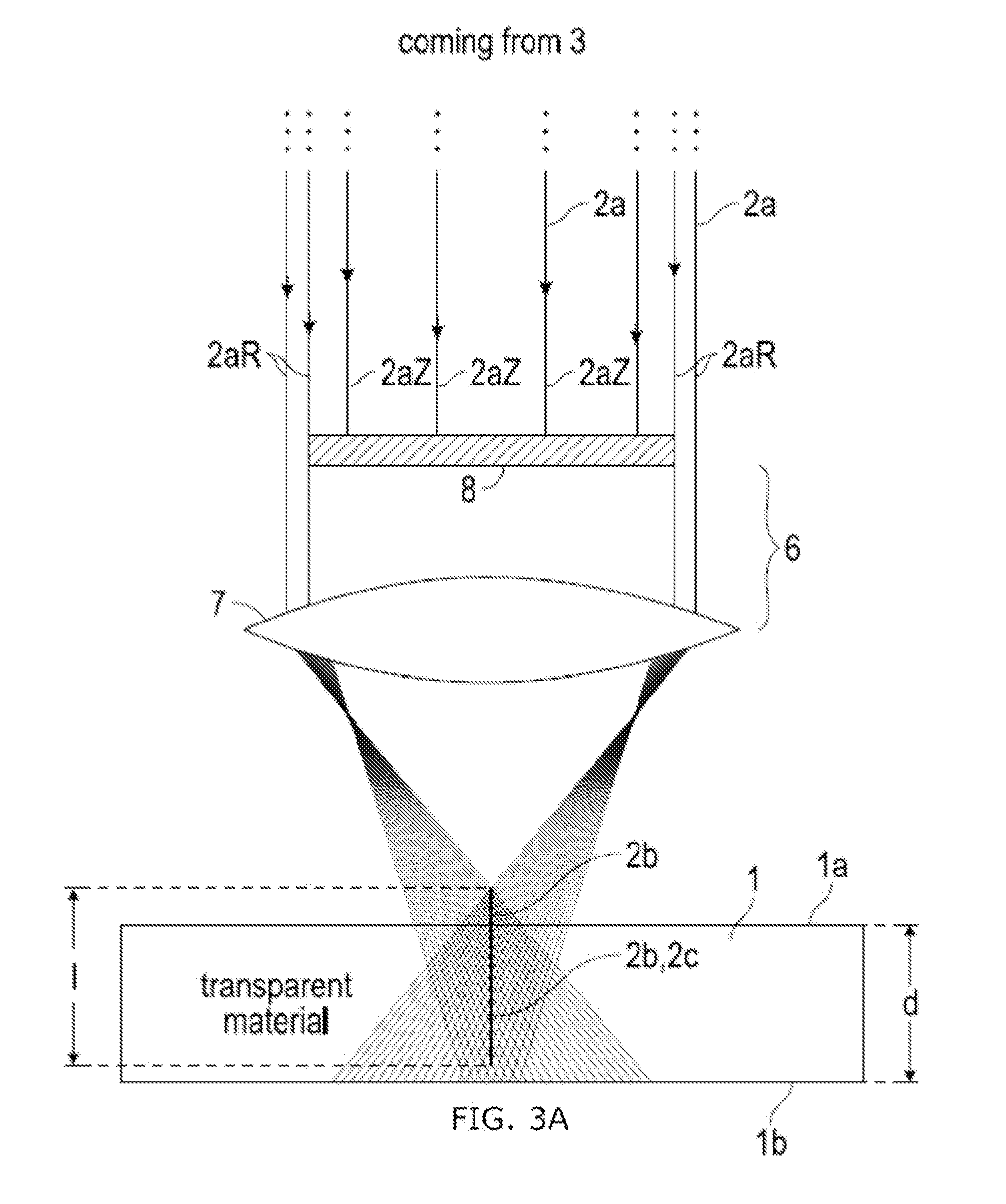
FIGS. 3B-1, 3B-2, 3B-3, and 3B-4 illustrate various possibilities for processing the substrate by forming the laser beam focal line at different positions within the transparent material relative to the substrate according to embodiments;
FIG. 4 is an illustration of a second optical assembly for laser processing according to an embodiment;
FIGS. 5A and 5B are illustrations of a third optical assembly for laser drilling according to an embodiment;
FIG. 6 is a schematic illustration of a fourth optical assembly for laser processing according to an embodiment;
FIG. 7 is a graph of laser emission as a function of time for a picosecond laser according to an embodiment, where each emission is characterized by a pulse "burst" which may contain one or more sub-pulses, the frequency of the bursts is the repetition rate of the laser, typically about 100 kHz (10 .mu.sec), and the time between sub-pulses is much shorter, e.g., about 20 nanoseconds (nsec);
FIG. 8 is a comparison between a focused Gaussian beam and a Bessel beam incident upon a glass-air-glass composite structure;
FIG. 9 is an illustration of stacking with transparent protective layers to cut multiple sheets while reducing abrasion or contamination according to an embodiment;
FIG. 10 is an illustration of an air gap and cutting of encapsulated devices according to an embodiment;
FIG. 11 is an illustration of cutting of interposers or windows with laser perforation then etch or laser perforation and CO.sub.2 laser release according to an embodiment;
FIG. 12 is an illustration of cutting an article such as electrochromic glass coated with transparent conductive layers (e.g. indium tin oxide (ITO)) according to an embodiment;
FIG. 13 is an illustration of precision cutting of some layers in a stack while not damaging others according to an embodiment;
FIG. 14a is a schematic top view representation of perforations formed in a glass substrate according to an embodiment;
FIG. 14b is a magnified view of D1 shown in FIG. 14a showing the local damage site with the perforation, the stress field and all micro cracks in a glass substrate according to an embodiment;
FIG. 15a is a side view of a glass substrate showing the interface of the glass substrate, a laser assembly connected to an optical assembly, a moving apparatus connected to the laser assembly and/or optical assembly, and a controller above the glass substrate according to an embodiment;
FIG. 15b is a magnified side view of D1 shown in FIG. 15a showing the local damage site with the perforation, the stress field and all micro cracks in a glass substrate according to an embodiment;
FIG. 15c is an illustrates of birefringence (retardation (nm),) due to the stress as function of distance from center of the perforation (x-axis).
FIG. 15d corresponds to FIG. 15c and illustrates stress values as function of distance from center of the perforation (x-axis).
FIG. 16 is a graphical illustration showing relative interface fracture toughness vs. average of the distances between perforation sites (D2)/average of the averaged characteristic crack lengths (D1/2) according to an embodiment;
FIGS. 17a-b are graphical illustrations showing relative interface fracture toughness of G2=glass-2 intermediate strength glass vs. actual average of the distances between perforation sites (D2) where actual particular averaged crack lengths are involved according to an embodiment;
FIG. 18 is a top view of a glass substrate illustrating the start of separation of the glass into components on opposite sides of a contour according to an embodiment;
FIG. 19 is a SEM image of a side view of the interface of a glass substrate post perforation formation and separation according to an embodiment;
FIG. 20 is a side view of a glass substrate showing the creation of damage only in at least one CS layer, without affecting the CT layer of a glass substrate according to an embodiment; and
FIG. 21 is an illustration of an alternative optical assembly for laser processing according to an embodiment.
DETAILED DESCRIPTION
A description of example embodiments follows.
The embodiment described herein relates to a method and apparatus for optically producing high precision cuts in or through transparent materials. Sub-surface damage may be limited to the order of 60 microns in depth or less, and the cuts may produce only low debris. Cutting of a transparent material with a laser in accordance with the present disclosure may also be referred to herein as drilling or laser drilling or laser processing. A material is substantially transparent to the laser wavelength when the absorption is less than about 10%, preferably less than about 1% per mm of material depth at this wavelength.
In accordance with methods described below, in a single pass, a laser can be used to create highly controlled full line perforation through the material, with extremely little (<75 .mu.m, often <50 .mu.m) subsurface damage and debris generation. This is in contrast to the typical use of spot-focused laser to ablate material, where multiple passes are often necessary to completely perforate the glass thickness, large amounts of debris are formed from the ablation process, and more extensive sub-surface damage (>100 .mu.m) and edge chipping occur.
Thus, it is possible to create a microscopic (i.e., <0.5 .mu.m and >100 nm in diameter) elongated "hole" (also called a perforation or a defect line) in transparent material using a single high energy burst pulse. These individual perforations can be created at rates of several hundred kilohertz (several hundred thousand perforations per second, for example). Thus, with relative motion between the source and the material these perforations can be placed adjacent to one another (spatial separation varying from sub-micron to several microns as desired). This spatial separation is selected in order to facilitate cutting. In some embodiments the defect line is a "through hole", which is a hole or an open channel that extends from the top to the bottom of the transparent material. In some embodiments the defect line may not be a continuous channel, and may be blocked or partially blocked by portions or sections of solid material (e.g., glass). As defined herein, the internal diameter of the defect line is the internal diameter of the open channel or the air hole. For example, in the embodiments described herein the internal diameter of the defect line is <500 nm, for example .ltoreq.400 nm, or .ltoreq.300 nm. The disrupted or modified area (e.g., compacted, melted, or otherwise changed) of the material surrounding the holes in the embodiments disclosed herein, preferably has diameter of <50 .mu.m (e.g., <10 .mu.m).
In addition, through judicious selection of optics, selective cut individual layers of stacked transparent materials. Micromachining and selective cutting of a stack of transparent materials is accomplished with precise control of the depth of cut through selection of an appropriate laser source and wavelength along with beam delivery optics, and the placement of a beam disruption element at the boundary of a desired layer. The beam disruption element may be a layer of material or an interface. The beam disruption element may be referred to herein as a laser beam disruption element, disruption element or the like. Embodiments of the beam disruption element may be referred to herein as a beam disruption layer, laser beam disruption layer, disruption layer, beam disruption interface, laser beam disruption interface, disruption interface, or the like.
The beam disruption element reflects, absorbs, scatters, defocuses or otherwise interferes with an incident laser beam to inhibit or prevent the laser beam from damaging or otherwise modifying underlying layers in the stack. In one embodiment, the beam disruption element underlies the layer of transparent material in which laser drilling will occur. As used herein, the beam disruption element underlies the transparent material when placement of the beam disruption element is such that the laser beam must pass through the transparent material before encountering the beam disruption element. The beam disruption element may underlie and be directly adjacent to the transparent layer in which laser drilling will occur. Stacked materials can be micro-machined or cut with high selectivity by inserting a layer or modifying the interface such that a contrast of optical properties exists between different layers of the stack. By making the interface between materials in the stack more reflective, absorbing, and/or scattering at the laser wavelengths of interest, cutting can be confined to one portion or layer of the stack.
The wavelength of the laser is selected so that the material within the stack to be laser processed (drilled, cut, ablated, damaged or otherwise appreciably modified by the laser) is transparent to the laser wavelength. In one embodiment, the material to be processed by the laser is transparent to the laser wavelength if it absorbs less than 10% of the intensity of the laser wavelength per mm of thickness of the material. In another embodiment, the material to be processed by the laser is transparent to the laser wavelength if it absorbs less than 5% of the intensity of the laser wavelength per mm of thickness of the material. In still another, the material to be processed by the laser is transparent to the laser wavelength if it absorbs less than 2% of the intensity of the laser wavelength per mm of thickness of the material. In yet another embodiment, the material to be processed by the laser is transparent to the laser wavelength if it absorbs less than 1% of the intensity of the laser wavelength per mm of thickness of the material.
The selection of the laser source is further predicated on the ability to induce multi-photon absorption (MPA) in the transparent material. MPA is the simultaneous absorption of multiple photons of identical or different frequencies in order to excite a material from a lower energy state (usually the ground state) to a higher energy state (excited state). The excited state may be an excited electronic state or an ionized state. The energy difference between the higher and lower energy states of the material is equal to the sum of the energies of the two photons. MPA is a third-order nonlinear process that is several orders of magnitude weaker than linear absorption. It differs from linear absorption in that the strength of absorption depends on the square of the light intensity, thus making it a nonlinear optical process. At ordinary light intensities, MPA is negligible. If the light intensity (energy density) is extremely high, such as in the region of focus of a laser source (particularly a pulsed laser source), MPA becomes appreciable and leads to measurable effects in the material within the region where the energy density of the light source is sufficiently high. Within the focal region, the energy density may be sufficiently high to result in ionization.
At the atomic level, the ionization of individual atoms has discrete energy requirements. Several elements commonly used in glass (e.g., Si, Na, K) have relatively low ionization energies (.about.5 eV). Without the phenomenon of MPA, a wavelength of about 248 nm would be required to create linear ionization at .about.5 eV. With MPA, ionization or excitation between states separated in energy by .about.5 eV can be accomplished with wavelengths longer than 248 nm. For example, photons with a wavelength of 532 nm have an energy of .about.2.33 eV, so two photons with wavelength 532 nm can induce a transition between states separated in energy by .about.4.66 eV in two-photon absorption (TPA), for example.
Thus, atoms and bonds can be selectively excited or ionized in the regions of a material where the energy density of the laser beam is sufficiently high to induce nonlinear TPA of a laser wavelength having half the required excitation energy, for example. MPA can result in a local reconfiguration and separation of the excited atoms or bonds from adjacent atoms or bonds. The resulting modification in the bonding or configuration can result in non-thermal ablation and removal of matter from the region of the material in which MPA occurs. This removal of matter creates a structural defect (e.g. a defect line or "perforation") that mechanically weakens the material and renders it more susceptible to cracking or fracturing upon application of mechanical or thermal stress. By controlling the placement of perforations, a contour or path along which cracking occurs can be precisely defined and precise micromachining of the material can be accomplished. The contour defined by a series of perforations may be regarded as a fault line and corresponds to a region of structural weakness in the material. In one embodiment, micromachining includes separation of a part from the material processed by the laser, where the part has a precisely defined shape or perimeter determined by a closed contour of perforations formed through MPA effects induced by the laser. As used herein, the term closed contour refers to a perforation path formed by the laser line, where the path intersects with itself at some location. An internal contour is a path formed where the resulting shape is entirely surrounded by an outer portion of material.
Perforations can be accomplished with a single "burst" of high energy short duration pulses spaced close together in time. The laser pulse duration may be 10.sup.-10 s or less, or 10.sup.-11 s or less, or 10.sup.-12 s or less, or 10.sup.-13 s or less. These "bursts" may be repeated at high repetition rates (e.g. kHz or MHz). The perforations may be spaced apart and precisely positioned by controlling the velocity of a substrate or stack relative to the laser through control of the motion of the laser and/or the substrate or stack.
As an example, in a thin transparent substrate moving at 200 mm/sec exposed to a 100 kHz series of pulses, the individual pulses would be spaced 2 microns apart to create a series of perforations separated by 2 microns. This defect (perforation) spacing is sufficient close to allow for mechanical or thermal separation along the contour defined by the series of perforations.
Thermal Separation:
In some cases, a fault line created along a contour defined by a series of perforations or defect lines is not enough to separate the part spontaneously, and a secondary step may be necessary. If so desired, a second laser can be used to create thermal stress to separate it, for example. In the case of sapphire, separation can be achieved, after the creation of a fault line, by application of mechanical force or by using a thermal source (e.g., an infrared laser, for example a CO.sub.2 laser) to create thermal stress and force a part to separate from a substrate. Another option is to have the CO.sub.2 laser only start the separation and then finish the separation manually. The optional CO.sub.2 laser separation can be achieved, for example, with a defocused continuous wave (cw) laser emitting at 10.6 .mu.m and with power adjusted by controlling its duty cycle. Focus change (i.e., extent of defocusing up to and including focused spot size) is used to vary the induced thermal stress by varying the spot size. Defocused laser beams include those laser beams that produce a spot size larger than a minimum, diffraction-limited spot size on the order of the size of the laser wavelength. For example, spot sizes of about 7 mm, 2 mm and 20 mm can be used for CO.sub.2 lasers, for example, whose emission wavelength is much smaller at 10.6 .mu.m. Distance between adjacent defect lines 120 along the direction of the fault lines 110 can be greater than 0.5 .mu.m and less than or equal to about 15 .mu.m in some embodiments, for example.
Etching:
Acid etching can be used, for example, to separate a workpiece having a glass layer, for example. To enlarge the holes to a size useful for metal filling and electrical connections, parts can be acid etched. In one embodiment, for example, the acid used can be 10% HF/15% HNO.sub.3 by volume. The parts can be etched for 53 minutes at a temperature of 24-25.degree. C. to remove about 100 .mu.m of material, for example. The parts can be immersed in this acid bath, and ultrasonic agitation at a combination of 40 kHz and 80 kHz frequencies can used to facilitate penetration of fluid and fluid exchange in the holes. In addition, manual agitation of the part within the ultrasonic field can be made to prevent standing wave patterns from the ultrasonic field from creating "hot spots" or cavitation related damage on the part. The acid composition and etch rate can be intentionally designed to slowly etch the part--a material removal rate of only 1.9 um/minute, for example. An etch rate of less than about 2 .mu.m/minute, for example, allows acid to fully penetrate the narrow holes and agitation to exchange fresh fluid and remove dissolved material from the holes which are initially very narrow.
In the embodiment shown in FIG. 1, precise control of the depth of cut in a multilayer stack is achieved by inclusion of a beam disruption interface (labeled "modified interface"). The beam disruption interface prevents the laser radiation from interacting with portions of the multilayer stack beyond the position of the disruption interface.
In one embodiment, the beam disruption element is positioned immediately below the layer of the stack in which modification via two-photon absorption will occur. Such a configuration is shown in FIG. 1, where the beam disruption element is a modified interface positioned immediately below material A and material A is the material in which formation of perforations through the two-photon absorption mechanism described herein will occur. As used herein, reference to a position below or lower than another position assumes that the top or uppermost position is the surface of the multilayer stack upon which the laser beam is first incident. In FIG. 1, for example, the surface of material A that is closest to the laser source is the top surface and placement of the beam disruption element below material A means that the laser beam traverses material A before interacting with the beam disruption element.
The disruption element has different optical properties than the material to be cut. For example, the beam disruption element may be a defocusing element, a scattering element, a translucent element, or a reflective element. A defocusing element is an interface or a layer comprising a material that prevents the laser light from forming the laser beam focal line on or below the defocusing element. The defocusing element may be comprised of a material or interface with refractive index inhomogeneities that scatter or perturb the wavefront of the optical beam. A translucent element is an interface or layer of material that allows light to pass through, but only after scattering or attenuating the laser beam to lower the energy density sufficiently to prevent formation of a laser beam focal line in portions of the stack on the side of the translucent element that are remote from the laser beam. In o
References
D00000
D00001
D00002
D00003
D00004
D00005
D00006
D00007
D00008
D00009
D00010
D00011
D00012

D00013

D00014

D00015

D00016

D00017

D00018

D00019

D00020

D00021

D00022

D00023

XML
uspto.report is an independent third-party trademark research tool that is not affiliated, endorsed, or sponsored by the United States Patent and Trademark Office (USPTO) or any other governmental organization. The information provided by uspto.report is based on publicly available data at the time of writing and is intended for informational purposes only.
While we strive to provide accurate and up-to-date information, we do not guarantee the accuracy, completeness, reliability, or suitability of the information displayed on this site. The use of this site is at your own risk. Any reliance you place on such information is therefore strictly at your own risk.
All official trademark data, including owner information, should be verified by visiting the official USPTO website at www.uspto.gov. This site is not intended to replace professional legal advice and should not be used as a substitute for consulting with a legal professional who is knowledgeable about trademark law.