Modified three-stage doherty amplifier
Grebennikov , et al.
U.S. patent number 10,601,375 [Application Number 16/150,156] was granted by the patent office on 2020-03-24 for modified three-stage doherty amplifier. This patent grant is currently assigned to SUMITOMO ELECTRONIC DEVICES INNOVATIONS, INC.. The grantee listed for this patent is SUMITOMO ELECTRIC DEVICE INNOVATIONS, INC.. Invention is credited to Andrey Grebennikov, Naoki Watanabe, James Wong.


| United States Patent | 10,601,375 |
| Grebennikov , et al. | March 24, 2020 |
Modified three-stage doherty amplifier
Abstract
A 3-stage Doherty amplifier that includes a three-way splitter, a carrier amplifier, first to second peak amplifiers, and an output combiner is disclosed. The output combiner includes first to fifth transmission lines with a .lamda./4 electrical length except for that in a downstream of the second peak amplifier, which provides a .lamda./2 electrical length. By dividing the latter transmission line into two parts each having a .lamda./4 length, and setting impedance thereof in a relation of (Z.sub.1/Z.sub.3).sup.2.times.(Z.sub.L/3), the output impedance of the respective amplifiers are common to each other to be Z.sub.o, where Z.sub.1, Z.sub.3, and Z.sub.L are impedance of the transmission liens in respective downstream sides of the amplifiers, that of the transmission line provided in the output, and the load impedance, respectively.
| Inventors: | Grebennikov; Andrey (Herts, GB), Wong; James (Surrey, GB), Watanabe; Naoki (London, GB) | ||||||||||
|---|---|---|---|---|---|---|---|---|---|---|---|
| Applicant: |
|
||||||||||
| Assignee: | SUMITOMO ELECTRONIC DEVICES
INNOVATIONS, INC. (Kanagawa, JP) |
||||||||||
| Family ID: | 65896240 | ||||||||||
| Appl. No.: | 16/150,156 | ||||||||||
| Filed: | October 2, 2018 |
Prior Publication Data
| Document Identifier | Publication Date | |
|---|---|---|
| US 20190103842 A1 | Apr 4, 2019 | |
Related U.S. Patent Documents
| Application Number | Filing Date | Patent Number | Issue Date | ||
|---|---|---|---|---|---|
| 62567519 | Oct 3, 2017 | ||||
| Current U.S. Class: | 1/1 |
| Current CPC Class: | H03F 3/21 (20130101); H03F 1/56 (20130101); H03F 1/0288 (20130101); H03F 2200/387 (20130101) |
| Current International Class: | H03F 1/07 (20060101); H03F 1/56 (20060101); H03F 1/02 (20060101); H03F 3/21 (20060101) |
| Field of Search: | ;330/124R,295 |
References Cited [Referenced By]
U.S. Patent Documents
| 8022760 | September 2011 | Gajadharsing |
| 8274332 | September 2012 | Cho |
| 8346189 | January 2013 | Dupuy |
| 8564367 | October 2013 | Svechtarov |
| 10187015 | January 2019 | Grebennikov |
| 2012/0126890 | May 2012 | Svechtarov |
| 2015/0333706 | November 2015 | Blednov |
Other References
|
Srirattana, Nuttapong, et al., Analysis and Design of a High-Efficiency Multistage Doherty Power Amplifier for Wireless Communication, IEEE Transactions on Microwave Theory & Techniques, vol. 53, No. 3, Mar. 2005. cited by applicant. |
Primary Examiner: Choe; Henry
Attorney, Agent or Firm: Smith, Gambrell & Russell, LLP
Parent Case Text
CROSS REFERENCE TO RELATED APPLICATION
This application claims benefit of U.S. Provisional Application No. 62/567,519, filed Oct. 3, 2017, the contents of which are incorporated by reference herein.
Claims
What is claimed is:
1. A three-stage Doherty amplifier, comprising: a three-way splitter that splits an input signal evenly into three portions; a carrier amplifier that receives one of the portions of the input signal split by the three-way splitter, the carrier amplifier always turning on for the input signal; first and second peak amplifiers each receiving respective other portions of the input signal split by the three-way splitter, the first peak amplifier turning on when input signal power becomes greater than a first back-off point, the second peak amplifier turning on when the input signal power becomes greater than a second back-off point greater than the first back-off point; and an output combiner that includes a first output transmission line set in a downstream side of the carrier amplifier, a second output transmission line set in a downstream side of the first peak amplifier, a third output transmission line set in a downstream side of the second peak amplifier, a fourth output transmission line set in a downstream side of the second output transmission line and the third output transmission line, and a fifth output transmission line set in a downstream side of the first output transmission line and the fourth output transmission line, wherein the first, second, fourth, and fifth output transmission lines have an electrical length of a quarter-wavelength (.lamda./4) and the third output transmission line has an electrical length of a half-wavelength (.lamda./2), where .lamda. is a wavelength of the input signal.
2. The Doherty amplifier according to claim 1, wherein the output combiner provides a first combining node and a second combining node, the first combining node combining the second output transmission line with the third output transmission line, the second combining node combining the first output transmission line with the fourth output transmission line.
3. The Doherty amplifier according to claim 2, wherein the fifth output transmission line is put between the second combining node and an output of the Doherty amplifier.
4. The Doherty amplifier according to claim 1, further including a first input transmission line and a second input transmission line, the first input transmission line having an electrical length of .lamda./2 and provided in an upstream side of the carrier amplifier, and the second input transmission line having an electrical length of .lamda./4 and provided in an upstream side of the first peak amplifier.
5. The Doherty amplifier according to claim 1, wherein the carrier amplifier, the first peak amplifier, and the second peak amplifier each implement devices with sizes substantially equal to each other.
6. The Doherty amplifier according to claim 5, wherein the carrier amplifier, and the first and second peak amplifiers include input matching circuits, output matching circuits, and offset lines for adjusting phases of signals output from the carrier amplifier and the first and second peak amplifiers.
7. The Doherty amplifier according to claim 1, wherein the third transmission line includes an upstream transmission line and a downstream transmission line connected in series to each other, the upstream transmission line and the downstream transmission line each having an electrical length of .lamda./4.
8. The Doherty amplifier according to claim 7, wherein the first output transmission line, the second output transmission line and the upstream transmission line have equal characteristic impedances.
9. The Doherty amplifier according to claim 8, wherein the carrier amplifier and the first and second peak amplifiers have load impedance of (Z.sub.1/Z.sub.3).sup.2.times.(Z.sub.L/3) common to each other, where Z.sub.1 is impedance of the first, second and upstream transmission lines, Z.sub.3 is impedance of the fifth transmission line, and Z.sub.L is load impedance.
Description
BACKGROUND OF INVENTION
1. Field of Invention
The present invention relates to a modification of a three-stage Doherty amplifier.
2. Related Background Arts
In modern telecommunication systems, it is required that the power amplifier could deliver a wide range of output powers with high efficiency and high linearity. Generally, being designed for the highest power level with maximum available efficiency, the power amplifiers in base stations tend to operate less efficiently at lower power levels consuming a lot of extra DC power. Besides, in those systems with an increased bandwidth and a high data rate, the transmitting signal is characterized by high peak-to-average power ratio due to wide and rapid variations of the instantaneous transmitting power. Therefore, it is a real challenge to design a power amplifier for a base station that has high efficiency not only at maximum output power but also at lower power levels typically ranging from -6 dB and smaller, with a minimum size and a lower cost of implementation.
N. Srirattana et. al has reported in IEEE Trans. Microwave Theory Technology, volume MTT-53, pages 852-860, March 2005, that the efficiency of a two-stage Doherty amplifier that provides a carrier amplifier and a single peak amplifier may be increased by extending the configuration thereof into a 3-stage Doherty amplifier by adding a second peak amplifier, which brings serious benefit when input signals have large peak-to-average ratios. One subject left in a conventional three-stage Doherty amplifier is that the load-line impedance seen by the carrier amplifier at lower power back-off causes heavy saturation of the carrier amplifier and, consequently, a significant degradation of the linearity between the input and the output of the Doherty amplifier. A typical technique for avoiding this degradation is to use complicated drive profiles at the input, thereby increasing the complexity of the input splitter. Another subject is that, in a case where the carrier amplifier and the peak amplifier have device sizes and configurations equal to each other, marginal improvement is obtained relative to the symmetrical two-stage Doherty amplifier. This requires selection of different transistor sizes and results in complicated device selection procedures.
SUMMARY OF INVENTION
An aspect of the present invention relates to a three-stage Doherty amplifier that includes a three-way splitter, a carrier amplifier, a first and second peak amplifiers, and an output combiner. The three-way splitter splits an input signal evenly into three portions. The carrier amplifier receives one of the portions of the input signal split by the three-way splitter and always turns on for the input signal. The first and second peak amplifiers receive the respective portions of the input signal split by the three-way splitter. The first peak amplifier turns on when the input signal in power thereof becomes greater than a first back-off point. The second peak amplifier turns on when the input signal in the power thereof becomes greater than a second back-off point that is greater than the first back-off point. The output combiner includes first to fifth output transmission lines, where the first to third output transmission lines are provided in downstream sides of the respective amplifiers. The fourth output transmission line is provided in a downstream side of the second output transmission line and the third output transmission line. The fifth output transmission line is provided in a downstream side of the first output transmission line and the fourth output transmission line. A feature of the Doherty amplifier of the embodiment is that the first to fifth output transmission lines except for the third output transmission line have an electrical length of a quarter-wavelength (.lamda./4); while, the third transmission line has an electrical length of a half-wavelength (.lamda./2), where .lamda. is a wavelength of the input signal.
DESCRIPTION OF DRAWINGS
The present disclosure may be better understood, and its numerous objects, features, and advantages made apparent to those skilled in the art by referencing the accompanying drawings:
FIG. 1 schematically shows a conventional three-stage Doherty amplifier;
FIG. 2 shows a schematic of a modified three-stage Doherty configuration according to the present invention; and
FIG. 3 shows another schematic of the three-stage Doherty amplifier modified from that shown in FIG. 2.
DESCRIPTION OF EMBODIMENT
FIG. 1 shows the schematic of a three-stage Doherty amplifier configuration disclosed in U.S. Pat. No. 8,022,760, where the output combiner 30 implements a phase shift of 90.degree. between an output of a carrier amplifier 10.sub.C and an amplifier output OUT, a phase shift of 180.degree. between an output of a first peak amplifier 10.sub.P1 and the amplifier output OUT, and a phase shift of 90.degree. between an output of a second peak amplifier 10.sub.p2 and the amplifier output OUT.
Thus, the output combiner 30 consists of the first quarter-wave (.lamda./4) transmission line TL.sub.O1 connected between the output of the carrier amplifier 10.sub.C and the amplifier output OUT, a second .lamda./4 transmission line TL.sub.O2 connected between the output of the first peak amplifier 10.sub.P1 and the output of the second peak amplifier 10.sub.P2, and a third .lamda./4 transmission line connected between the output of the second peak amplifier 10.sub.P2 and the amplifier output OUT when the output of the second peak amplifier 10.sub.P2 is directly connected with a node N.sub.1 between the second .lamda./4 transmission line TL.sub.O2 and the third .lamda./4 transmission line TLo6.
The .lamda./4 transmission line TL.sub.I1 between a 3-way splitter divider 20 and the input of the carrier amplifier 10.sub.C and that TL.sub.I2 between the 3-way splitter 20 and the input of the second peak amplifier 10.sub.P2 are necessary to compensate for the phase delay caused in the output combiner 30. When three amplifiers have sizes whose ratio is simply given by 1:1:1, the first efficiency back-off point is obtained at -6 dB and the maximum efficiency back-off point is provided at -9.5 dB. However, for high-power applications, there is a difficulty to match the output combining scheme to the optimum load impedance of a transistor because the optimum load impedance thereof becomes very small at high power levels when a micro-strip line is hard or substantially impossible to physically implement such low enough characteristic impedance and the second peak amplifier 10.sub.P2 is also hard or impossible to be directly connected with the node between the second .lamda./4 transmission line TL.sub.O2 and the third .lamda./4 transmission line TLo3.
Therefore, for convenience of the circuit implementation, the three-stage Doherty amplifier configuration shown in FIG. 1 may be modified by including of an additional half-wave transmission line at the output of the second peak amplifier 10.sub.P2 and an additional .lamda./4 transmission line may be included between the second combining node N.sub.2 and the amplifier output OUT in order to secure the design flexibility in choosing optimum values of the transmission-line characteristic impedance required at different output power levels.
The present invention provides a modified three-stage Doherty amplifier including a carrier amplifier 10.sub.C and two peak amplifiers, 10.sub.P1 and 10.sub.P2, each having an input matching circuit, an output matching circuit, and an offset line, when the carrier amplifier 10.sub.C and the peak amplifiers, 10.sub.P1 and 10.sub.P2, are configured to operate such that the peak amplifiers, 10.sub.P1 and 10.sub.P2, switch on sequentially under an increase in input power; an input 3-way splitter 20 is coupled between an input IN of the Doherty amplifier and inputs of the carrier amplifier 10.sub.C and the peak amplifiers, 10.sub.P1 and 10.sub.P2, the outputs of the carrier amplifier 10.sub.C and the peak amplifiers, 10.sub.P1 and 10.sub.P2, are coupled through an output impedance combiner 30 to the output OUT of the Doherty amplifier. The first peak amplifier 10.sub.P1 is coupled with the second peak amplifier 10.sub.P2 at the first combining node N.sub.1 through the .lamda./4 transmission line TL.sub.O2 and the third transmission line TL.sub.O3 with an electrical length of .lamda./2, and then both peak amplifiers, 10.sub.P1 and 10.sub.P2, are coupled at the second combining node N.sub.2 with the carrier amplifier 10.sub.C through the transmission lines, TL.sub.O1 and TL.sub.O4, respectively. The first peak amplifier 10.sub.P1 is coupled with the input splitter 20 through the .DELTA./4 transmission line TL.sub.I2, while the carrier amplifier 10.sub.C is coupled with the input splitter 20 through the .lamda./2 transmission line TL.sub.I1. The .lamda./4 impedance transformer, which is a .lamda./4 transmission line TL.sub.O5, connected between the second combining node N.sub.2 and the output of output combiner 30 provides a function of output impedance transformation.
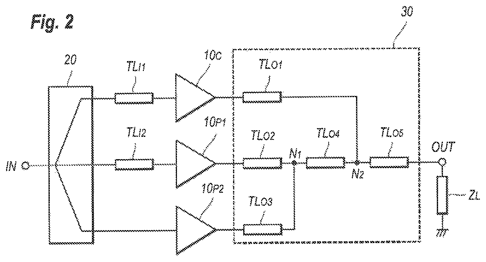
FIG. 2 shows the schematic of a modified three-stage Doherty amplifier according to embodiment of the present invention, where the modifier Doherty amplifier shown in FIG. 2 provides an additional .lamda./4 transmission line TL.sub.O4 between the second combining node N.sub.2 and the amplifier output OUT for enhancing the design flexibility of choosing optimum values of the transmission-line characteristic impedances required at different output power levels.
Also, the modified Doherty amplifier further includes an additional .lamda./2 transmission line TL.sub.O3 at the output of the second peak amplifier 10.sub.P2 to simplify the physical connection of the second peak amplifier 10.sub.P2 with a path for the first peak amplifier 10.sub.P1 without changing impedance conditions under circuit implementation on a printed circuit board. All amplifiers, 10.sub.C, 10.sub.P1, and 10.sub.P2, include the input matching circuits, the output matching circuits, and the offset lines, which are not illustrated in the figures, necessary to provide high impedance at their outputs for peak amplifiers, 10.sub.P1 and 10.sub.P2, when they are turned off.
All amplifiers, 10.sub.C, 10.sub.P1 and 10.sub.P2, are turned on at saturation, the carrier amplifier 10.sub.C is turned on only to provide efficiency peak at maximum back-off of -9.5 dB when the peak amplifiers, 10.sub.P1 and 10.sub.P2, are turned off; and both the carrier amplifier 10.sub.C and the first peak amplifier 10.sub.P1 are turned on to provide efficiency peak at -6 dB. In the latter situation, the .lamda./2 transmission line TL.sub.I1 provided at the input of the carrier amplifier 10.sub.C and the .lamda./4 transmission line TL.sub.I2 set upstream of the first peak amplifier 10.sub.P1 are required to compensate for the phase delay caused in the output combiner 30.
FIG. 3 shows another embodiment of the modified three-stage Doherty amplifier according to the present invention, where the Doherty amplifier shown in FIG. 3 provides, substituted from the .lamda./2 transmission line TL.sub.O3 at the output of the second peak amplifier 10.sub.P2 shown in FIG. 2, two .lamda./4 transmission lines, TL.sub.O3a and TL.sub.O3b, to implement capability in transforming the impedance in the output combiner 30, which may be called as a upstream transmission lien and a downstream transmission line, respectively. In this case, the load impedance seen by the carrier amplifier 10.sub.C and two peak amplifiers, 10.sub.P1 and 10.sub.P2, may vary depending on the characteristic impedance of the corresponding .lamda./4 lines, TL.sub.O1, TL.sub.O2, and TL.sub.O3a, provided in the respective outputs of the amplifiers, 10.sub.C, 10.sub.P1, and 10.sub.P2.
In a case of a balanced Doherty amplifier where the carrier and two peak amplifiers, 10.sub.C, 10.sub.P1 and 10.sub.P2 have a ratio in the device size thereof to be equal to 1:1:1 and optimum load impedance of Z.sub.o; the characteristic impedance of the .lamda./4 transmission lines, TL.sub.O1, TL.sub.O2, and TL.sub.O3a, connected with the respective outputs of the carrier and two peak amplifier, 10.sub.C, 10.sub.P1, and 10.sub.P2, may be set as Z.sub.1= (Z.sub.oZ.sub.2), where Z.sub.2 is the characteristic impedance of the downstream transmission line TL.sub.O3b provided in a downstream side of the upstream transmission line TL.sub.O3a. The downstream transmission line TL.sub.O3b is connected with the path for the first peak amplifier 10.sub.P1 between two .lamda./4 transmission lines, TL.sub.O2 and TLo4, one of which TL.sub.O2 has the characteristic impedance Z.sub.1, while, the other TLo4 has the characteristic impedance Z.sub.2/2, where Z.sub.2=3Z.sub.3.sup.2/Z.sub.L and Z.sub.3 is the characteristic impedance of the .lamda./4 transmission line TL.sub.O5 connected between the second combining node N.sub.2 and the amplifier output OUT.
For the case without impedance transformation in the output combiner 30, when conditions of Z.sub.3=28.9.OMEGA. and Z.sub.L=50.OMEGA. are assumed, a relation of Z.sub.o=Z.sub.1=Z.sub.2=50.OMEGA. may be obtained. However, when other conditions of Z.sub.3=40.8.OMEGA. and Z.sub.L=50.OMEGA. are assumed, the characteristic impedance Z.sub.2 of the .lamda./4 transmission line TL.sub.O4 is necessary to be increased to 100.OMEGA.. In this case, when the .lamda./4 transmission lines, TL.sub.O1, TL.sub.O2, and TL.sub.O3a, set in the respective outputs of the carrier amplifier and two peak amplifiers, 10.sub.C, 10.sub.P1, and 10.sub.P2, to be Z.sub.1=50.OMEGA.; the load impedance Z.sub.o of the respective amplifiers, 10.sub.C, 10.sub.P1, and 10.sub.P2, reduces to Z.sub.o=25.OMEGA. which is two times smaller than the value without impedance transformation. The same load impedance of Z.sub.o=25.OMEGA. may be achieved for conditions of Z.sub.1=35.3.OMEGA., Z.sub.2=50.OMEGA., and Z.sub.3=28.9.OMEGA.. Generally, depending on the value of Z.sub.3 and Z.sub.1, the load impedance Z.sub.o may be set to any desired value according to Z.sub.o=(Z.sub.1/Z.sub.3).sup.2(Z.sub.L/3) for fixed Z.sub.L.
* * * * *
D00000
D00001
D00002
D00003
XML
uspto.report is an independent third-party trademark research tool that is not affiliated, endorsed, or sponsored by the United States Patent and Trademark Office (USPTO) or any other governmental organization. The information provided by uspto.report is based on publicly available data at the time of writing and is intended for informational purposes only.
While we strive to provide accurate and up-to-date information, we do not guarantee the accuracy, completeness, reliability, or suitability of the information displayed on this site. The use of this site is at your own risk. Any reliance you place on such information is therefore strictly at your own risk.
All official trademark data, including owner information, should be verified by visiting the official USPTO website at www.uspto.gov. This site is not intended to replace professional legal advice and should not be used as a substitute for consulting with a legal professional who is knowledgeable about trademark law.