Pixel circuits for AMOLED displays
Azizi , et al.
U.S. patent number 10,593,263 [Application Number 15/888,451] was granted by the patent office on 2020-03-17 for pixel circuits for amoled displays. This patent grant is currently assigned to Ignis Innovation Inc.. The grantee listed for this patent is Ignis Innovation Inc.. Invention is credited to Yaser Azizi, Gholamreza Chaji.


| United States Patent | 10,593,263 |
| Azizi , et al. | March 17, 2020 |
Pixel circuits for AMOLED displays
Abstract
The OLED voltage of a selected pixel is extracted from the pixel produced when the pixel is programmed so that the pixel current is a function of the OLED voltage. One method for extracting the OLED voltage is to first program the pixel in a way that the current is not a function of OLED voltage, and then in a way that the current is a function of OLED voltage. During the latter stage, the programming voltage is changed so that the pixel current is the same as the pixel current when the pixel was programmed in a way that the current was not a function of OLED voltage. The difference in the two programming voltages is then used to extract the OLED voltage.
| Inventors: | Azizi; Yaser (Waterloo, CA), Chaji; Gholamreza (Waterloo, CA) | ||||||||||
|---|---|---|---|---|---|---|---|---|---|---|---|
| Applicant: |
|
||||||||||
| Assignee: | Ignis Innovation Inc.
(Waterloo, CA) |
||||||||||
| Family ID: | 50193282 | ||||||||||
| Appl. No.: | 15/888,451 | ||||||||||
| Filed: | February 5, 2018 |
Prior Publication Data
| Document Identifier | Publication Date | |
|---|---|---|
| US 20180158411 A1 | Jun 7, 2018 | |
Related U.S. Patent Documents
| Application Number | Filing Date | Patent Number | Issue Date | ||
|---|---|---|---|---|---|
| 15494951 | Apr 24, 2017 | 9922596 | |||
| 15133318 | May 23, 2017 | 9659527 | |||
| 13789978 | May 24, 2016 | 9351368 | |||
| Current U.S. Class: | 1/1 |
| Current CPC Class: | G09G 3/3258 (20130101); G09G 3/3233 (20130101); H05B 45/14 (20200101); G09G 2300/0842 (20130101); G09G 2320/10 (20130101); G09G 2320/0295 (20130101); G09G 2320/0693 (20130101); G09G 2320/045 (20130101); G09G 2320/048 (20130101); G09G 2300/0819 (20130101) |
| Current International Class: | G09G 3/3233 (20160101); H05B 33/08 (20200101); G09G 3/3258 (20160101) |
References Cited [Referenced By]
U.S. Patent Documents
| 3506851 | April 1970 | Polkinghorn |
| 3750987 | August 1973 | Gobel |
| 3774055 | November 1973 | Bapat |
| 4090096 | May 1978 | Nagami |
| 4354162 | October 1982 | Wright |
| 4996523 | February 1991 | Bell |
| 5134387 | July 1992 | Smith |
| 5153420 | October 1992 | Hack |
| 5170158 | December 1992 | Shinya |
| 5204661 | April 1993 | Hack |
| 5266515 | November 1993 | Robb |
| 5278542 | January 1994 | Smith |
| 5408267 | April 1995 | Main |
| 5498880 | March 1996 | Lee |
| 5572444 | November 1996 | Lentz |
| 5589847 | December 1996 | Lewis |
| 5619033 | April 1997 | Weisfield |
| 5648276 | July 1997 | Hara |
| 5670973 | September 1997 | Bassetti |
| 5691783 | November 1997 | Numao |
| 5701505 | December 1997 | Yamashita |
| 5714968 | February 1998 | Ikeda |
| 5744824 | April 1998 | Kousai |
| 5745660 | April 1998 | Kolpatzik |
| 5748160 | May 1998 | Shieh |
| 5758129 | May 1998 | Gray |
| 5835376 | November 1998 | Smith |
| 5870071 | February 1999 | Kawahata |
| 5874803 | February 1999 | Garbuzov |
| 5880582 | March 1999 | Sawada |
| 5903248 | May 1999 | Irwin |
| 5917280 | June 1999 | Burrows |
| 5949398 | September 1999 | Kim |
| 5952789 | September 1999 | Stewart |
| 5990629 | November 1999 | Yamada |
| 6023259 | February 2000 | Howard |
| 6069365 | May 2000 | Chow |
| 6091203 | July 2000 | Kawashima |
| 6097360 | August 2000 | Holloman |
| 6100868 | August 2000 | Lee |
| 6144222 | November 2000 | Ho |
| 6229506 | May 2001 | Dawson |
| 6229508 | May 2001 | Kane |
| 6246180 | June 2001 | Nishigaki |
| 6252248 | June 2001 | Sano |
| 6268841 | July 2001 | Cairns |
| 6288696 | September 2001 | Holloman |
| 6307322 | October 2001 | Dawson |
| 6310962 | October 2001 | Chung |
| 6323631 | November 2001 | Juang |
| 6333729 | December 2001 | Ha |
| 6384804 | May 2002 | Dodabalapur |
| 6388653 | May 2002 | Goto |
| 6392617 | May 2002 | Gleason |
| 6396469 | May 2002 | Miwa |
| 6414661 | July 2002 | Shen |
| 6417825 | July 2002 | Stewart |
| 6430496 | August 2002 | Smith |
| 6433488 | August 2002 | Bu |
| 6473065 | October 2002 | Fan |
| 6475845 | November 2002 | Kimura |
| 6501098 | December 2002 | Yamazaki |
| 6501466 | December 2002 | Yamagashi |
| 6522315 | February 2003 | Ozawa |
| 6535185 | March 2003 | Kim |
| 6542138 | April 2003 | Shannon |
| 6559839 | May 2003 | Ueno |
| 6580408 | June 2003 | Bae |
| 6583398 | June 2003 | Harkin |
| 6618030 | September 2003 | Kane |
| 6639244 | October 2003 | Yamazaki |
| 6680580 | January 2004 | Sung |
| 6686699 | February 2004 | Yumoto |
| 6690000 | February 2004 | Muramatsu |
| 6693610 | February 2004 | Shannon |
| 6694248 | February 2004 | Smith |
| 6697057 | February 2004 | Koyama |
| 6724151 | April 2004 | Yoo |
| 6734636 | May 2004 | Sanford |
| 6753655 | June 2004 | Shih |
| 6753834 | June 2004 | Mikami |
| 6756741 | June 2004 | Li |
| 6756958 | June 2004 | Furuhashi |
| 6777888 | August 2004 | Kondo |
| 6781567 | August 2004 | Kimura |
| 6788231 | September 2004 | Hsueh |
| 6809706 | October 2004 | Shimoda |
| 6828950 | December 2004 | Koyama |
| 6858991 | February 2005 | Miyazawa |
| 6859193 | February 2005 | Yumoto |
| 6876346 | April 2005 | Anzai |
| 6900485 | May 2005 | Lee |
| 6903734 | June 2005 | Eu |
| 6911960 | June 2005 | Yokoyama |
| 6911964 | June 2005 | Lee |
| 6914448 | July 2005 | Jinno |
| 6919871 | July 2005 | Kwon |
| 6924602 | August 2005 | Komiya |
| 6937220 | August 2005 | Kitaura |
| 6940214 | September 2005 | Komiya |
| 6954194 | October 2005 | Matsumoto |
| 6970149 | November 2005 | Chung |
| 6975142 | December 2005 | Azami |
| 6975332 | December 2005 | Arnold |
| 6995519 | February 2006 | Arnold |
| 7027015 | April 2006 | Booth, Jr. |
| 7034793 | April 2006 | Sekiya |
| 7038392 | May 2006 | Libsch |
| 7057588 | June 2006 | Asano |
| 7061451 | June 2006 | Kimura |
| 7071932 | July 2006 | Libsch |
| 7106285 | September 2006 | Naugler |
| 7112820 | September 2006 | Chang |
| 7113864 | September 2006 | Smith |
| 7122835 | October 2006 | Ikeda |
| 7129914 | October 2006 | Knapp |
| 7164417 | January 2007 | Cok |
| 7224332 | May 2007 | Cok |
| 7248236 | July 2007 | Nathan |
| 7259737 | August 2007 | Ono |
| 7262753 | August 2007 | Tanghe |
| 7274363 | September 2007 | Ishizuka |
| 7310092 | December 2007 | Imamura |
| 7315295 | January 2008 | Kimura |
| 7317434 | January 2008 | Lan |
| 7321348 | January 2008 | Cok |
| 7327357 | February 2008 | Jeong |
| 7333077 | February 2008 | Koyama |
| 7343243 | March 2008 | Smith |
| 7414600 | August 2008 | Nathan |
| 7466166 | December 2008 | Date |
| 7495501 | February 2009 | Iwabuchi |
| 7502000 | March 2009 | Yuki |
| 7515124 | April 2009 | Yaguma |
| 7535449 | May 2009 | Miyazawa |
| 7554512 | June 2009 | Steer |
| 7569849 | August 2009 | Nathan |
| 7595776 | September 2009 | Hashimoto |
| 7604718 | October 2009 | Zhang |
| 7609239 | October 2009 | Chang |
| 7612745 | November 2009 | Yumoto |
| 7619594 | November 2009 | Hu |
| 7619597 | November 2009 | Nathan |
| 7639211 | December 2009 | Miyazawa |
| 7683899 | March 2010 | Hirakata |
| 7688289 | March 2010 | Abe |
| 7760162 | July 2010 | Miyazawa |
| 7808008 | October 2010 | Miyake |
| 7859520 | December 2010 | Kimura |
| 7889159 | February 2011 | Nathan |
| 7903127 | March 2011 | Kwon |
| 7920116 | April 2011 | Woo |
| 7944414 | May 2011 | Shirasaki |
| 7978170 | July 2011 | Park |
| 7989392 | August 2011 | Crockett |
| 7995008 | August 2011 | Miwa |
| 8040303 | October 2011 | Kim et al. |
| 8063852 | November 2011 | Kwak |
| 8102343 | January 2012 | Yatabe |
| 8144081 | March 2012 | Miyazawa |
| 8159007 | April 2012 | Barna |
| 8237746 | August 2012 | Betts-LaCroix |
| 8242979 | August 2012 | Anzai |
| 8253665 | August 2012 | Nathan |
| 8283967 | October 2012 | Chaji |
| 8319712 | November 2012 | Nathan |
| 8564513 | October 2013 | Nathan |
| 8872739 | October 2014 | Kimura |
| 9351368 | May 2016 | Azizi |
| 9430958 | August 2016 | Chaji |
| 9466240 | October 2016 | Jaffari |
| 9472138 | October 2016 | Nathan |
| 9659527 | May 2017 | Williams |
| 9685114 | July 2017 | Chaji |
| 9697771 | July 2017 | Azizi |
| 9721505 | August 2017 | Chaji |
| 9741292 | August 2017 | Nathan |
| 9747834 | August 2017 | Chaji |
| RE46561 | September 2017 | Chaji |
| 9922596 | March 2018 | Azizi |
| 2001/0002703 | June 2001 | Koyama |
| 2001/0009283 | July 2001 | Arao |
| 2001/0024186 | September 2001 | Kane |
| 2001/0026257 | October 2001 | Kimura |
| 2001/0030323 | October 2001 | Ikeda |
| 2001/0035863 | November 2001 | Kimura |
| 2001/0040541 | November 2001 | Yoneda |
| 2001/0043173 | November 2001 | Troutman |
| 2001/0045929 | November 2001 | Prache |
| 2001/0052940 | December 2001 | Hagihara |
| 2002/0000576 | January 2002 | Inukai |
| 2002/0011796 | January 2002 | Koyama |
| 2002/0011799 | January 2002 | Kimura |
| 2002/0012057 | January 2002 | Kimura |
| 2002/0030190 | March 2002 | Ohtani |
| 2002/0047565 | April 2002 | Nara |
| 2002/0052086 | May 2002 | Maeda |
| 2002/0080108 | June 2002 | Wang |
| 2002/0084463 | July 2002 | Sanford |
| 2002/0101172 | August 2002 | Bu |
| 2002/0117722 | August 2002 | Osada |
| 2002/0140712 | October 2002 | Ouchi |
| 2002/0158587 | October 2002 | Komiya |
| 2002/0158666 | October 2002 | Azami |
| 2002/0158823 | October 2002 | Zavracky |
| 2002/0171613 | November 2002 | Goto |
| 2002/0181275 | December 2002 | Yamazaki |
| 2002/0186214 | December 2002 | Siwinski |
| 2002/0190971 | December 2002 | Nakamura |
| 2002/0195967 | December 2002 | Kim |
| 2002/0195968 | December 2002 | Sanford |
| 2002/0196213 | December 2002 | Akimoto |
| 2003/0001828 | January 2003 | Asano |
| 2003/0001858 | January 2003 | Jack |
| 2003/0016190 | January 2003 | Kondo |
| 2003/0020413 | January 2003 | Oomura |
| 2003/0030603 | February 2003 | Shimoda |
| 2003/0062524 | April 2003 | Kimura |
| 2003/0062844 | April 2003 | Miyazawa |
| 2003/0076048 | April 2003 | Rutherford |
| 2003/0090445 | May 2003 | Chen |
| 2003/0090447 | May 2003 | Kimura |
| 2003/0090481 | May 2003 | Kimura |
| 2003/0095087 | May 2003 | Libsch |
| 2003/0098829 | May 2003 | Chen |
| 2003/0107560 | June 2003 | Yumoto |
| 2003/0107561 | June 2003 | Uchino |
| 2003/0111966 | June 2003 | Mikami |
| 2003/0112205 | June 2003 | Yamada |
| 2003/0112208 | June 2003 | Okabe |
| 2003/0117348 | June 2003 | Knapp |
| 2003/0122474 | July 2003 | Lee |
| 2003/0122747 | July 2003 | Shannon |
| 2003/0128199 | July 2003 | Kimura |
| 2003/0151569 | August 2003 | Lee |
| 2003/0156104 | August 2003 | Morita |
| 2003/0169241 | September 2003 | LeChevalier |
| 2003/0169247 | September 2003 | Kawabe |
| 2003/0174152 | September 2003 | Noguchi |
| 2003/0179626 | September 2003 | Sanford |
| 2003/0185438 | October 2003 | Osawa |
| 2003/0189535 | October 2003 | Matsumoto |
| 2003/0197663 | October 2003 | Lee |
| 2003/0214465 | November 2003 | Kimura |
| 2003/0227262 | December 2003 | Kwon |
| 2003/0230141 | December 2003 | Gilmour |
| 2003/0230980 | December 2003 | Forrest |
| 2004/0004589 | January 2004 | Shih |
| 2004/0032382 | February 2004 | Cok |
| 2004/0041750 | March 2004 | Abe |
| 2004/0066357 | April 2004 | Kawasaki |
| 2004/0070557 | April 2004 | Asano |
| 2004/0070558 | April 2004 | Cok |
| 2004/0090186 | May 2004 | Yoshida |
| 2004/0095338 | May 2004 | Takashi |
| 2004/0129933 | July 2004 | Nathan |
| 2004/0130516 | July 2004 | Nathan |
| 2004/0135749 | July 2004 | Kondakov |
| 2004/0145547 | July 2004 | Oh |
| 2004/0150595 | August 2004 | Kasai |
| 2004/0155841 | August 2004 | Kasai |
| 2004/0160516 | August 2004 | Ford |
| 2004/0171619 | September 2004 | Barkoczy |
| 2004/0174349 | September 2004 | Libsch |
| 2004/0174354 | September 2004 | Ono |
| 2004/0183759 | September 2004 | Stevenson |
| 2004/0189627 | September 2004 | Shirasaki |
| 2004/0196275 | October 2004 | Hattori |
| 2004/0227697 | November 2004 | Mori |
| 2004/0239696 | December 2004 | Okabe |
| 2004/0251844 | December 2004 | Hashido |
| 2004/0252085 | December 2004 | Miyagawa |
| 2004/0252089 | December 2004 | Ono |
| 2004/0256617 | December 2004 | Yamada |
| 2004/0257353 | December 2004 | Imamura |
| 2004/0257355 | December 2004 | Naugler |
| 2004/0263437 | December 2004 | Hattori |
| 2005/0007357 | January 2005 | Yamashita |
| 2005/0052379 | March 2005 | Waterman |
| 2005/0057459 | March 2005 | Miyazawa |
| 2005/0067970 | March 2005 | Libsch |
| 2005/0067971 | March 2005 | Kane |
| 2005/0083270 | April 2005 | Miyazawa |
| 2005/0110420 | May 2005 | Arnold |
| 2005/0110727 | May 2005 | Shin |
| 2005/0123193 | June 2005 | Lamberg |
| 2005/0140600 | June 2005 | Kim |
| 2005/0140610 | June 2005 | Smith |
| 2005/0145891 | July 2005 | Abe |
| 2005/0156831 | July 2005 | Yamazaki |
| 2005/0168416 | August 2005 | Hashimoto |
| 2005/0206590 | September 2005 | Sasaki |
| 2005/0212787 | September 2005 | Noguchi |
| 2005/0219188 | October 2005 | Kawabe |
| 2005/0243037 | November 2005 | Eom |
| 2005/0248515 | November 2005 | Naugler |
| 2005/0258867 | November 2005 | Miyazawa |
| 2005/0285822 | December 2005 | Reddy |
| 2005/0285825 | December 2005 | Eom |
| 2006/0012311 | January 2006 | Ogawa |
| 2006/0022305 | February 2006 | Yamashita |
| 2006/0038750 | February 2006 | Inoue |
| 2006/0038758 | February 2006 | Routley |
| 2006/0038762 | February 2006 | Chou |
| 2006/0066533 | March 2006 | Sato |
| 2006/0077077 | April 2006 | Kwon |
| 2006/0077134 | April 2006 | Hector |
| 2006/0077194 | April 2006 | Jeong |
| 2006/0092185 | May 2006 | Jo |
| 2006/0114196 | June 2006 | Shin |
| 2006/0125408 | June 2006 | Nathan |
| 2006/0125740 | June 2006 | Shirasaki |
| 2006/0139253 | June 2006 | Choi |
| 2006/0145964 | July 2006 | Park |
| 2006/0158402 | July 2006 | Nathan |
| 2006/0191178 | August 2006 | Sempel |
| 2006/0208971 | September 2006 | Deane |
| 2006/0209012 | September 2006 | Hagood, IV |
| 2006/0214888 | September 2006 | Schneider |
| 2006/0221009 | October 2006 | Miwa |
| 2006/0227082 | October 2006 | Ogata |
| 2006/0232522 | October 2006 | Roy |
| 2006/0244391 | November 2006 | Shishido |
| 2006/0244697 | November 2006 | Lee |
| 2006/0261841 | November 2006 | Fish |
| 2006/0279478 | December 2006 | Ikegami |
| 2006/0290614 | December 2006 | Nathan |
| 2007/0001939 | January 2007 | Hashimoto |
| 2007/0001945 | January 2007 | Yoshida |
| 2007/0008251 | January 2007 | Kohno |
| 2007/0008297 | January 2007 | Bassetti |
| 2007/0035489 | February 2007 | Lee |
| 2007/0035707 | February 2007 | Margulis |
| 2007/0040773 | February 2007 | Lee |
| 2007/0040782 | February 2007 | Woo |
| 2007/0057873 | March 2007 | Uchino |
| 2007/0057874 | March 2007 | Le Roy |
| 2007/0063932 | March 2007 | Nathan |
| 2007/0075957 | April 2007 | Chen |
| 2007/0080908 | April 2007 | Nathan |
| 2007/0085801 | April 2007 | Park |
| 2007/0109232 | May 2007 | Yamamoto |
| 2007/0128583 | June 2007 | Miyazawa |
| 2007/0164941 | July 2007 | Park |
| 2007/0182671 | August 2007 | Nathan |
| 2007/0236430 | October 2007 | Fish |
| 2007/0236440 | October 2007 | Wacyk |
| 2007/0241999 | October 2007 | Lin |
| 2007/0242008 | October 2007 | Cummings |
| 2008/0001544 | January 2008 | Murakami |
| 2008/0043044 | February 2008 | Woo |
| 2008/0048951 | February 2008 | Naugler |
| 2008/0055134 | March 2008 | Li |
| 2008/0062106 | March 2008 | Tseng |
| 2008/0074360 | March 2008 | Lu |
| 2008/0088549 | April 2008 | Nathan |
| 2008/0094426 | April 2008 | Kimpe |
| 2008/0111766 | May 2008 | Uchino |
| 2008/0122819 | May 2008 | Cho |
| 2008/0129906 | June 2008 | Lin |
| 2008/0198103 | August 2008 | Toyomura |
| 2008/0219232 | September 2008 | Heubel et al. |
| 2008/0228562 | September 2008 | Smith |
| 2008/0231625 | September 2008 | Minami |
| 2008/0231641 | September 2008 | Miyashita |
| 2008/0265786 | October 2008 | Koyama |
| 2008/0290805 | November 2008 | Yamada |
| 2009/0009459 | January 2009 | Miyashita |
| 2009/0015532 | January 2009 | Katayama |
| 2009/0058789 | March 2009 | Hung |
| 2009/0121988 | May 2009 | Amo |
| 2009/0146926 | June 2009 | Sung |
| 2009/0153448 | June 2009 | Tomida |
| 2009/0153459 | June 2009 | Han |
| 2009/0174628 | July 2009 | Wang |
| 2009/0201230 | August 2009 | Smith |
| 2009/0201281 | August 2009 | Routley |
| 2009/0206764 | August 2009 | Schemmann |
| 2009/0225011 | September 2009 | Choi |
| 2009/0244046 | October 2009 | Seto |
| 2009/0251486 | October 2009 | Sakakibara |
| 2009/0278777 | November 2009 | Wang |
| 2009/0289964 | November 2009 | Miyachi |
| 2009/0295423 | December 2009 | Levey |
| 2010/0026725 | February 2010 | Smith |
| 2010/0033469 | February 2010 | Nathan |
| 2010/0039451 | February 2010 | Jung |
| 2010/0039453 | February 2010 | Nathan |
| 2010/0045646 | February 2010 | Kishi |
| 2010/0079419 | April 2010 | Shibusawa |
| 2010/0134475 | June 2010 | Ogura |
| 2010/0141564 | June 2010 | Choi |
| 2010/0149223 | June 2010 | Betts-LaCroix |
| 2010/0207920 | August 2010 | Chaji |
| 2010/0225634 | September 2010 | Levey |
| 2010/0251295 | September 2010 | Amento |
| 2010/0269889 | October 2010 | Reinhold |
| 2010/0277400 | November 2010 | Jeong |
| 2010/0315319 | December 2010 | Cok |
| 2010/0315449 | December 2010 | Chaji |
| 2011/0050741 | March 2011 | Jeong |
| 2011/0063197 | March 2011 | Chung |
| 2011/0069089 | March 2011 | Kopf |
| 2011/0074762 | March 2011 | Shirasaki |
| 2011/0084993 | April 2011 | Kawabe |
| 2011/0109350 | May 2011 | Chaji |
| 2011/0169805 | July 2011 | Katsunori |
| 2011/0191042 | August 2011 | Chaji |
| 2011/0205221 | August 2011 | Lin |
| 2012/0026146 | February 2012 | Kim |
| 2012/0169793 | July 2012 | Nathan |
| 2012/0293478 | November 2012 | Chaji |
| 2012/0299976 | November 2012 | Chen |
| 2012/0299978 | November 2012 | Chaji |
| 2014/0267215 | September 2014 | Soni |
| 729652 | Jun 1997 | AU | |||
| 764896 | Dec 2001 | AU | |||
| 1 294 034 | Jan 1992 | CA | |||
| 2 249 592 | Jul 1998 | CA | |||
| 2 303 302 | Mar 1999 | CA | |||
| 2 368 386 | Sep 1999 | CA | |||
| 2 242 720 | Jan 2000 | CA | |||
| 2 354 018 | Jun 2000 | CA | |||
| 2 432 530 | Jul 2002 | CA | |||
| 2 436 451 | Aug 2002 | CA | |||
| 2 507 276 | Aug 2002 | CA | |||
| 2 463 653 | Jan 2004 | CA | |||
| 2 498 136 | Mar 2004 | CA | |||
| 2 522 396 | Nov 2004 | CA | |||
| 2 438 363 | Feb 2005 | CA | |||
| 2 443 206 | Mar 2005 | CA | |||
| 2 519 097 | Mar 2005 | CA | |||
| 2 472 671 | Dec 2005 | CA | |||
| 2 523 841 | Jan 2006 | CA | |||
| 2 567 076 | Jan 2006 | CA | |||
| 2 495 726 | Jul 2006 | CA | |||
| 2 557 713 | Nov 2006 | CA | |||
| 2 526 782 | Aug 2007 | CA | |||
| 2 651 893 | Nov 2007 | CA | |||
| 2 672 590 | Oct 2009 | CA | |||
| 1180418 | Apr 1998 | CN | |||
| 1588521 | Mar 2005 | CN | |||
| 1601594 | Mar 2005 | CN | |||
| 1886774 | Dec 2006 | CN | |||
| 101395653 | Mar 2009 | CN | |||
| 101908316 | Dec 2010 | CN | |||
| 103562989 | Feb 2014 | CN | |||
| 202006007613 | Sep 2006 | DE | |||
| 0 478 186 | Apr 1992 | EP | |||
| 0811866 | Dec 1997 | EP | |||
| 1 028 471 | Aug 2000 | EP | |||
| 1 130 565 | Sep 2001 | EP | |||
| 1 194 013 | Apr 2002 | EP | |||
| 1 321 922 | Jun 2003 | EP | |||
| 1 335 430 | Aug 2003 | EP | |||
| 1 381 019 | Jan 2004 | EP | |||
| 1 429 312 | Jun 2004 | EP | |||
| 1 439 520 | Jul 2004 | EP | |||
| 1 465 143 | Oct 2004 | EP | |||
| 1 473 689 | Nov 2004 | EP | |||
| 1 517 290 | Mar 2005 | EP | |||
| 1 521 203 | Apr 2005 | EP | |||
| 2 399 935 | Sep 2004 | GB | |||
| 2 460 018 | Nov 2009 | GB | |||
| 09 090405 | Apr 1997 | JP | |||
| 10-254410 | Sep 1998 | JP | |||
| 11 231805 | Aug 1999 | JP | |||
| 2002-278513 | Sep 2002 | JP | |||
| 2003-076331 | Mar 2003 | JP | |||
| 2003-099000 | Apr 2003 | JP | |||
| 2003-173165 | Jun 2003 | JP | |||
| 2003-186439 | Jul 2003 | JP | |||
| 2003-195809 | Jul 2003 | JP | |||
| 2003-271095 | Sep 2003 | JP | |||
| 2003-308046 | Oct 2003 | JP | |||
| 2004-054188 | Feb 2004 | JP | |||
| 2004-226960 | Aug 2004 | JP | |||
| 2005-004147 | Jan 2005 | JP | |||
| 2005-099715 | Apr 2005 | JP | |||
| 2005-258326 | Sep 2005 | JP | |||
| 2005-338819 | Dec 2005 | JP | |||
| 569173 | Jan 2004 | TW | |||
| 200526065 | Aug 2005 | TW | |||
| 1239501 | Sep 2005 | TW | |||
| WO 98/11554 | Mar 1998 | WO | |||
| WO 99/48079 | Sep 1999 | WO | |||
| WO 01/27910 | Apr 2001 | WO | |||
| WO 02/067327 | Aug 2002 | WO | |||
| WO 03/034389 | Apr 2003 | WO | |||
| WO 03/063124 | Jul 2003 | WO | |||
| WO 03/075256 | Sep 2003 | WO | |||
| WO 2004/003877 | Jan 2004 | WO | |||
| WO 2004/015668 | Feb 2004 | WO | |||
| WO 2004/034364 | Apr 2004 | WO | |||
| WO 2005/022498 | Mar 2005 | WO | |||
| WO 2005/055185 | Jun 2005 | WO | |||
| WO 2005/055186 | Jun 2005 | WO | |||
| WO 2005/069267 | Jul 2005 | WO | |||
| WO 2005/122121 | Dec 2005 | WO | |||
| WO 2006/063448 | Jun 2006 | WO | |||
| WO 2006/128069 | Nov 2006 | WO | |||
| WO 2007/079572 | Jul 2007 | WO | |||
| WO 2008/057369 | May 2008 | WO | |||
| WO 2009/059028 | May 2009 | WO | |||
| WO 2009/127065 | Oct 2009 | WO | |||
| WO 2010/066030 | Jun 2010 | WO | |||
| WO 2010/120733 | Oct 2010 | WO | |||
Other References
|
Ahnood et al.: "Effect of threshold voltage instability on field effect mobility in thin film transistors deduced from constant current measurements"; dated Aug. 2009. cited by applicant . Alexander et al.: "Pixel circuits and drive schemes for glass and elastic AMOLED displays"; dated Jul. 2005 (9 pages). cited by applicant . Alexander et al.: "Unique Electrical Measurement Technology for Compensation Inspection and Process Diagnostics of AMOLED HDTV"; dated May 2010 (4 pages). cited by applicant . Ashtiani et al.: "AMOLED Pixel Circuit With Electronic Compensation of Luminance Degradation"; dated Mar. 2007 (4 pages). cited by applicant . Chaji et al.: "A Current-Mode Comparator for Digital Calibration of Amorphous Silicon AMOLED Displays"; dated Jul. 2008 (5 pages). cited by applicant . Chaji et al.: "A fast settling current driver based on the CCII for AMOLED displays"; dated Dec. 2009 (6 pages). cited by applicant . Chaji et al.: "A Low-Cost Stable Amorphous Silicon AMOLED Display with Full V.about.T- and V.about.O.about.L.about.E.about.D Shift Compensation"; dated May 2007 (4 pages). cited by applicant . Chaji et al.: "A low-power driving scheme for a-Si:H active-matrix organic light-emitting diode displays"; dated Jun. 2005 (4 pages). cited by applicant . Chaji et al.: "A low-power high-performance digital circuit for deep submicron technologies"; dated Jun. 2005 (4 pages). cited by applicant . Chaji et al.: "A novel a-Si:H AMOLED pixel circuit based on short-term stress stability of a-Si:H TFTs"; dated Oct. 2005 (3 pages). cited by applicant . Chaji et al.: "A Novel Driving Scheme and Pixel Circuit for AMOLED Displays"; dated Jun. 2006 (4 pages). cited by applicant . Chaji et al.: "A novel driving scheme for high-resolution large-area a-Si:H AMOLED displays"; dated Aug. 2005 (4 pages). cited by applicant . Chaji et al.: "A Stable Voltage-Programmed Pixel Circuit for a-Si:H AMOLED Displays"; dated Dec. 2006 (12 pages). cited by applicant . Chaji et al.: "A Sub-.mu.A fast-settling current-programmed pixel circuit for AMOLED displays"; dated Sep. 2007. cited by applicant . Chaji et al.: "An Enhanced and Simplified Optical Feedback Pixel Circuit for AMOLED Displays"; dated Oct. 2006. cited by applicant . Chaji et al.: "Compensation technique for DC and transient instability of thin film transistor circuits for large-area devices"; dated Aug. 2008. cited by applicant . Chaji et al.: "Driving scheme for stable operation of 2-TFT a-Si AMOLED pixel"; dated Apr. 2005 (2 pages). cited by applicant . Chaji et al.: "Dynamic-effect compensating technique for stable a-Si:H AMOLED displays"; dated Aug. 2005 (4 pages). cited by applicant . Chaji et al.: "Electrical Compensation of OLED Luminance Degradation"; dated Dec. 2007 (3 pages). cited by applicant . Chaji et al.: "eUTDSP: a design study of a new VLIW-based DSP architecture"; dated May 2003 (4 pages). cited by applicant . Chaji et al.: "Fast and Offset-Leakage Insensitive Current-Mode Line Driver for Active Matrix Displays and Sensors"; dated Feb. 2009 (8 pages). cited by applicant . Chaji et al.: "High Speed Low Power Adder Design With a New Logic Style: Pseudo Dynamic Logic (SDL)"; dated Oct. 2001 (4 pages). cited by applicant . Chaji et al.: "High-precision fast current source for large-area current-programmed a-Si flat panels"; dated Sep. 2006 (4 pages). cited by applicant . Chaji et al.: "Low-Cost AMOLED Television with IGNIS Compensating Technology"; dated May 2008 (4 pages). cited by applicant . Chaji et al.: "Low-Cost Stable a-Si:H AMOLED Display for Portable Applications"; dated Jun. 2006 (4 pages). cited by applicant . Chaji et al.: "Low-Power Low-Cost Voltage-Programmed a-Si:H AMOLED Display"; dated Jun. 2008 (5 pages). cited by applicant . Chaji et al.: "Merged phototransistor pixel with enhanced near infrared response and flicker noise reduction for biomolecular imaging"; dated Nov. 2008 (3 pages). cited by applicant . Chaji et al.: "Parallel Addressing Scheme for Voltage-Programmed Active-Matrix OLED Displays"; dated May 2007 (6 pages). cited by applicant . Chaji et al.: "Pseudo dynamic logic (SDL): a high-speed and low-power dynamic logic family"; dated 2002 (4 pages). cited by applicant . Chaji et al.: "Stable a-Si:H circuits based on short-term stress stability of amorphous silicon thin film transistors"; dated May 2006 (4 pages). cited by applicant . Chaji et al.: "Stable Pixel Circuit for Small-Area High- Resolution a-Si:H AMOLED Displays"; dated Oct. 2008 (6 pages). cited by applicant . Chaji et al.: "Stable RGBW AMOLED display with OLED degradation compensation using electrical feedback"; dated Feb. 2010 (2 pages). cited by applicant . Chaji et al.: "Thin-Film Transistor Integration for Biomedical Imaging and AMOLED Displays"; dated May 2008 (177 pages). cited by applicant . Chapter 3: Color Spaces" Keith Jack: "Video Demystified: "A Handbook for the Digital Engineer" 2001 Referex ORD-0000-00-00 USA EP040425529 ISBN: 1-878707-56-6 pp. 32-33. cited by applicant . Chapter 8: Alternative Flat Panel Display 1-25 Technologies; Willem den Boer: "Active Matrix Liquid Crystal Display: Fundamentals and Applications" 2005 Referex ORD-0000-00-00 U.K.; XP040426102 ISBN: 0-7506-7813-5 pp. 206-209 p. 208. cited by applicant . European Partial Search Report Application No. 12 15 6251.6 European Patent Office dated May 30 2012 (7 pages). cited by applicant . European Patent Office Communication Application No. 05 82 1114 dated Jan. 11, 2013 (9 pages). cited by applicant . European Patent Office Communication with Supplemental European Search Report for EP Application No. 07 70 1644.2 dated Aug. 18, 2009 (12 pages). cited by applicant . European Search Report Application No. 10 83 4294.0-1903 dated Apr. 8, 2013 (9 pages). cited by applicant . European Search Report Application No. EP 05 80 7905 dated Apr. 2, 2009 (5 pages). cited by applicant . European Search Report Application No. EP 05 82 1114 dated Mar. 27 2009 (2 pages). cited by applicant . European Search Report Application No. EP 07 70 1644 dated Aug. 5, 2009. cited by applicant . European Search Report Application No. EP 10 17 5764 dated Oct. 18, 2010 (2 pages). cited by applicant . European Search Report Application No. EP 10 82 9593.2 European Patent Office dated May 17, 2013 (7 pages). cited by applicant . European Search Report Application No. EP 12 15 6251.6 European Patent Office dated Oct. 12, 2012 (18 pages). cited by applicant . European Search Report Application No. EP. 11 175 225.9 dated Nov. 4, 2011 (9 pages). cited by applicant . European Supplementary Search Report Application No. EP 09 80 2309 dated May 8, 2011 (14 pages). cited by applicant . European Supplementary Search Report Application No. EP 09 83 1339.8 dated Mar. 26, 2012 (11 pages). cited by applicant . Extended European Search Report Application No. EP 06 75 2777.0 dated Dec. 6, 2010 (21 pages). cited by applicant . Extended European Search Report Application No. EP 09 73 2338.0 dated May 24, 2011 (8 pages). cited by applicant . Extended European Search Report Application No. EP 11 17 5223, 4 dated Nov. 8, 2011 (8 pages). cited by applicant . Extended European Search Report Application No. EP 12 17 4465.0 European Patent Office dated Sep. 7, 2012 (9 pages). cited by applicant . Fan et al. "LTPS_TFT Pixel Circuit Compensation for TFT Threshold Voltage Shift and IR-Drop on the Power Line for Amolded Displays" 5 pages copyright 2012. cited by applicant . Goh et al. "A New a-Si:H Thin-Film Transistor Pixel Circuit for Active-Matrix Organic Light-Emitting Diodes" IEEE Electron Device Letters vol. 24 No. 9 Sep. 2003 pp. 583-585. cited by applicant . International Search Report Application No. PCT/CA2005/001844 dated Mar. 28, 2006 (2 pages). cited by applicant . International Search Report Application No. PCT/CA2006/000941 dated Oct. 3, 2006 (2 pages). cited by applicant . International Search Report Application No. PCT/CA2007/000013 dated May 7, 2007. cited by applicant . International Search Report Application No. PCT/CA2009/001049 dated Dec. 7, 2009 (4 pages). cited by applicant . International Search Report Application No. PCT/CA2009/001769 dated Apr. 8, 2010. cited by applicant . International Search Report Application No. PCT/IB2010/002898 Canadian Intellectual Property Office dated Jul. 28, 2009 (5 pages). cited by applicant . International Search Report Application No. PCT/IB2010/055481 dated Apr. 7, 2011 (3 pages). cited by applicant . International Search Report Application No. PCT/IB2011/051103 dated Jul. 8, 2011 3 pages. cited by applicant . International Search Report Application No. PCT/IB2012/052651 5 pages dated Sep. 11, 2012. cited by applicant . International Searching Authority Written Opinion Application No. PCT/IB2010/055481 dated Apr. 7, 2011 (6 pages). cited by applicant . International Searching Authority Written Opinion Application No. PCT/IB2012/052651 6 pages dated Sep. 11, 2012. cited by applicant . International Searching Authority Written Opinion Application No. PCT/IB2011/051103 dated Jul. 8, 2011 6 pages. cited by applicant . International Searching Authority Written Opinion Application No. PCT/IB2010/002898 Canadian Intellectual Property Office dated Mar. 30, 2011 (8 pages). cited by applicant . International Searching Authority Written Opinion Application No. PCT/CA2009/001769 dated Apr. 8, 2010 (8 pages). cited by applicant . Jafarabadiashtiani et al.: "A New Driving Method for a-Si AMOLED Displays Based on Voltage Feedback"; dated May 2005 (4 pages). cited by applicant . Lee et al.: "Ambipolar Thin-Film Transistors Fabricated by PECVD Nanocrystalline Silicon"; dated May 2006 (6 pages). cited by applicant . Ma e y et al: "Organic Light-Emitting Diode/Thin Film Transistor Integration for foldable Displays" Conference record of the 1997 International display research conference and international workshops on LCD technology and emissive technology. Toronto Sep. 15-19, 1997 (6 pages). cited by applicant . Matsueda y et al.: "35.1: 2.5-in. AMOLED with Integrated 6-bit Gamma Compensated Digital Data Driver"; dated May 2004 (4 pages). cited by applicant . Nathan et al. "Amorphous Silicon Thin Film Transistor Circuit Integration for Organic LED Displays on Glass and Plastic" IEEE Journal of Solid-State Circuits vol. 39 No. 9 Sep. 2004 pp. 1477-1486. cited by applicant . Nathan et al.: "Backplane Requirements for Active Matrix Organic Light Emitting Diode Displays"; dated Sep. 2006 (16 pages). cited by applicant . Nathan et al.: "Call for papers second international workshop on compact thin-film transistor (TFT) modeling for circuit simulation"; dated Sep. 2009 (1 page). cited by applicant . Nathan et al.: "Driving schemes for a-Si and LTPS AMOLED displays"; dated Dec. 2005 (11 pages). cited by applicant . Nathan et al.: "Invited Paper: a -Si for AMOLED--Meeting the Performance and Cost Demands of Display Applications (Cell Phone to HDTV)"; dated Jun. 2006 (4 pages). cited by applicant . Nathan et al.: "Thin film imaging technology on glass and plastic"; dated Oct. 31-Nov. 2, 2000 (4 pages). cited by applicant . Ono et al. "Shared Pixel Compensation Circuit for AM-OLED Displays " Proceedings of the 9.sup.th Asian Symposium on Information Display (ASID) pp. 462-465 New Delhi dated Oct. 8-12, 2006 (4 pages). cited by applicant . Philipp: "Charge transfer sensing" Sensor Review vol. 19 No. 2 Dec. 31, 1999 (Dec. 31, 1999) 10 pages. cited by applicant . Rafati et al.: "Comparison of a 17 b multiplier in Dual-rail domino and in Dual-rail D L (D L) logic styles"; dated 2002 (4 pages). cited by applicant . Safavaian et al.: "Three-TFT image sensor for real-time digital X-ray imaging"; dated Feb. 2, 2006 (2 pages). cited by applicant . Safavian et al.: "3-TFT active pixel sensor with correlated double sampling readout circuit for real-time medical x-ray imaging"; dated Jun. 2006 (4 pages). cited by applicant . Safavian et al.: "A novel current scaling active pixel sensor with correlated double sampling readout circuit for real time medical x-ray imaging"; dated May 2007 (7 pages). cited by applicant . Safavian et al.: "A novel hybrid active-passive pixel with correlated double sampling CMOS readout circuit for medical x-ray imaging"; dated May 2008 (4 pages). cited by applicant . Safavian et al.: "Self-compensated a-Si:H detector with current-mode readout circuit for digital X-ray fluoroscopy"; dated Aug. 2005 (4 pages). cited by applicant . Safavian et al.: "TFT active image sensor with current-mode readout circuit for digital x-ray fluoroscopy [5969D-82]"; dated Sep. 2005 (9 pages). cited by applicant . Smith, Lindsay I., "A tutorial on Principal Components Analysis," dated Feb. 26, 2001 (27 pages). cited by applicant . Stewart M. et al. "Polysilicon TFT technology for active matrix OLED displays" IEEE transactions on electron devices vol. 48 No. May 5, 2001 (7 pages). cited by applicant . Vygranenko et al.: "Stability of indium-oxide thin-film transistors by reactive ion beam assisted deposition"; dated Feb. 2009. cited by applicant . Wang et al.: "Indium oxides by reactive ion beam assisted evaporation: From material study to device application," dated Mar. 2009 (6 pages). cited by applicant . Yi He et al. "Current-Source a-Si:H Thin Film Transistor Circuit for Active-Matrix Organic Light-Emitting Displays" IEEE Electron Device Letters vol. 21 No. 12 Dec. 2000 pp. 590-592. cited by applicant . International Search Report Application No. PCT/IB2013/059074, dated Dec. 18, 2013 (5 pages). cited by applicant . International Searching Authority Written Opinion Application No. PCT/IB2013/059074, dated Dec. 18, 2013 (8 pages). cited by applicant . Extended European Search Report Application No. EP 15173106.4 dated Oct. 15, 2013 (8 pages). cited by applicant . International Search Report Application No. PCT/IB2017/050170, dated May 5, 2017 (3 pages). cited by applicant . International Searching Authority Written Opinion Application No. PCT/IB2017/050170, dated May 5, 2017 (4 pages). cited by applicant. |
Primary Examiner: Xavier; Antonio
Attorney, Agent or Firm: Stratford Managers Corporation
Parent Case Text
CROSS REFERENCE TO RELATED APPLICATIONS
This application is a continuation of U.S. patent application Ser. No. 15/494,951, filed Apr. 24, 2017, now allowed, which is a continuation of U.S. patent application Ser. No. 15/133,318, filed Apr. 20, 2016, now U.S. Pat. No. 9,659,527, which is a continuation of and claims the benefit of U.S. patent application Ser. No. 13/789,978, filed Mar. 8, 2013, now U.S. Pat. No. 9,351,368, both of which are hereby incorporated by reference herein in their entireties.
Claims
What is claimed is:
1. A method of determining the current effective voltage V.sub.OLED of a light-emitting device in a selected pixel in an array of pixels in a display in which each pixel includes a light-emitting device and a drive transistor for supplying current to said light-emitting device, said method comprising storing a programming voltage in the selected pixel using the light-emitting device of the selected pixel, the stored programming voltage being a function of the current effective voltage V.sub.OLED of said light-emitting device, supplying current to said light-emitting device via said drive transistor in said selected pixel according to said stored programming voltage, said current being a function of the current effective voltage V.sub.OLED of said light-emitting device, measuring said current, and extracting the value of the current effective voltage V.sub.OLED of said light-emitting device from said current measurement.
2. The method of claim 1 in which said light-emitting devices are OLEDs.
3. The method of claim 1 in which said current is supplied to said light-emitting device via a drive transistor in each pixel.
4. The method of claim 1 in which said current is measured via a read transistor in each pixel.
5. A method of determining the current effective voltage V.sub.OLED of a light-emitting device in a selected pixel in an array of pixels in a display in which each pixel includes a light-emitting device and a drive transistor for supplying current to said light-emitting device, said method comprising supplying a first predetermined programming voltage to said selected pixel to store a first programming voltage in the selected pixel, the stored first programming voltage being independent of the current effective voltage V.sub.OLED of said light-emitting device, supplying a first current to said light-emitting device in said selected pixel according to said stored first programming voltage, said first current being independent of the effective voltage V.sub.OLED of said light-emitting device, measuring said first current, supplying a second predetermined programming voltage to said selected pixel to store a second programming voltage in the selected pixel using the light-emitting device of the selected pixel, the stored second programming voltage being a function of the current effective voltage V.sub.OLED of said light-emitting device, supplying a second current to said light-emitting device in said selected pixel according to said stored second programming voltage, said second current being a function of the current effective voltage V.sub.OLED of said light-emitting device, measuring said second current, and extracting the value of the current effective voltage V.sub.OLED of said light-emitting device from the difference between said first and second currents and current-voltage characteristics of said selected pixel.
6. A system for determining the current effective voltage V.sub.OLED of a light-emitting device of a selected pixel in an array of pixels in a display in which each pixel includes a light-emitting device and a drive transistor for supplying current to the light-emitting device, the system comprising a controller adapted to store a programming voltage in the selected pixel using the light-emitting device of the selected pixel, the stored programming voltage being a function of the current effective voltage V.sub.OLED of said light-emitting device, supply current to said light-emitting device via said drive transistor in said selected pixel according to said stored programming voltage, said current being a function of the current effective voltage V.sub.OLED of said light-emitting device, measure said current, and extract the value of the current effective voltage V.sub.OLED of said light-emitting device from said current measurement.
Description
FIELD OF THE INVENTION
The present disclosure generally relates to circuits for use in displays, and methods of driving, calibrating, and programming displays, particularly displays such as active matrix organic light emitting diode displays.
BACKGROUND
Displays can be created from an array of light emitting devices each controlled by individual circuits (i.e., pixel circuits) having transistors for selectively controlling the circuits to be programmed with display information and to emit light according to the display information. Thin film transistors ("TFTs") fabricated on a substrate can be incorporated into such displays. TFTs tend to demonstrate non-uniform behavior across display panels and over time as the displays age. Compensation techniques can be applied to such displays to achieve image uniformity across the displays and to account for degradation in the displays as the displays age.
Some schemes for providing compensation to displays to account for variations across the display panel and over time utilize monitoring systems to measure time dependent parameters associated with the aging (i.e., degradation) of the pixel circuits. The measured information can then be used to inform subsequent programming of the pixel circuits so as to ensure that any measured degradation is accounted for by adjustments made to the programming. Such monitored pixel circuits may require the use of additional transistors and/or lines to selectively couple the pixel circuits to the monitoring systems and provide for reading out information. The incorporation of additional transistors and/or lines may undesirably decrease pixel-pitch (i.e., "pixel density").
SUMMARY
In accordance with one embodiment, the OLED voltage of a selected pixel is extracted from the pixel produced when the pixel is programmed so that the pixel current is a function of the OLED voltage. One method for extracting the OLED voltage is to first program the pixel in a way that the current is not a function of OLED voltage, and then in a way that the current is a function of OLED voltage. During the latter stage, the programming voltage is changed so that the pixel current is the same as the pixel current when the pixel was programmed in a way that the current was not a function of OLED voltage. The difference in the two programming voltages is then used to extract the OLED voltage.
Another method for extracting the OLED voltage is to measure the difference between the current of the pixel when it is programmed with a fixed voltage in both methods (being affected by OLED voltage and not being affected by OLED voltage). This measured difference and the current-voltage characteristics of the pixel are then used to extract the OLED voltage.
A further method for extracting the shift in the OLED voltage is to program the pixel for a given current at time zero (before usage) in a way that the pixel current is a function of OLED voltage, and save the programming voltage. To extract the OLED voltage shift after some usage time, the pixel is programmed for the given current as was done at time zero. To get the same current as time zero, the programming voltage needs to change. The difference in the two programming voltages is then used to extract the shift in the OLED voltage. Here one needs to remove the effect of TFT aging from the second programming voltage first; this is done by programming the pixel without OLED effect for a given current at time zero and after usage. The difference in the programming voltages in this case is the TFT aging, which is subtracted from the calculated different in the aforementioned case.
In one implementation, the current effective voltage V.sub.OLED of a light-emitting device in a selected pixel is determined by supplying a programming voltage to the drive transistor in the selected pixel to supply a first current to the light-emitting device (the first current being independent of the effective voltage V.sub.OLED of the light-emitting device), measuring the first current, supplying a second programming voltage to the drive transistor in the selected pixel to supply a second current to the light-emitting device, the second current being a function of the current effective voltage V.sub.OLED of the light-emitting device, measuring the second current and comparing the first and second current measurements, adjusting the second programming voltage to make the second current substantially the same as the first current, and extracting the value of the current effective voltage V.sub.OLED of the light-emitting device from the difference between the first and second programming voltages.
In another implementation, the current effective voltage V.sub.OLED of a light-emitting device in a selected pixel is determined by supplying a first programming voltage to the drive transistor in the selected pixel to supply a first current to the light-emitting device in the selected pixel (the first current being independent of the effective voltage V.sub.OLED of the light-emitting device), measuring the first current, supplying a second programming voltage to the drive transistor in the selected pixel to supply a second current to the light-emitting device in the selected pixel (the second current being a function of the current effective voltage V.sub.OLED of the light-emitting device), measuring the second current, and extracting the value of the current effective voltage V.sub.OLED of the light-emitting device from the difference between the first and second current measurements.
In a modified implementation, the current effective voltage V.sub.OLED of a light-emitting device in a selected pixel is determined by supplying a first programming voltage to the drive transistor in the selected pixel to supply a predetermined current to the light-emitting device at a first time (the first current being a function of the effective voltage V.sub.OLED of the light-emitting device), supplying a second programming voltage to the drive transistor in the selected pixel to supply the predetermined current to the light-emitting device at a second time following substantial usage of the display, and extracting the value of the current effective voltage V.sub.OLED of the light-emitting device from the difference between the first and second programming voltages.
In another modified implementation, the current effective voltage V.sub.OLED of a light-emitting device in a selected pixel is determined by supplying a predetermined programming voltage to the drive transistor in the selected pixel to supply a first current to the light-emitting device (the first current being independent of the effective voltage V.sub.OLED of the light-emitting device), measuring the first current, supplying the predetermined programming voltage to the drive transistor in the selected pixel to supply a second current to the light-emitting device (the second current being a function of the current effective voltage V.sub.OLED of the light-emitting device), measuring the second current, and extracting the value of the current effective voltage V.sub.OLED of the light-emitting device from the difference between the first and second currents and current-voltage characteristics of the selected pixel.
In a preferred implementation, a system is provided for controlling an array of pixels in a display in which each pixel includes a light-emitting device. Each pixel includes a pixel circuit that comprises the light-emitting device, which emits light when supplied with a voltage V.sub.OLED; a drive transistor for driving current through the light-emitting device according to a driving voltage across the drive transistor during an emission cycle, the drive transistor having a gate, a source and a drain and characterized by a threshold voltage; and a storage capacitor coupled across the source and gate of the drive transistor for providing the driving voltage to the drive transistor. A supply voltage source is coupled to the drive transistor for supplying current to the light-emitting device via the drive transistor, the current being controlled by the driving voltage. A monitor line is coupled to a read transistor that controls the coupling of the monitor line to a first node that is common to the source side of the storage capacitor, the source of the drive transistor, and the light-emitting device. A data line is coupled to a switching transistor that controls the coupling of the data line to a second node that is common to the gate side of the storage capacitor and the gate of the drive transistor. A controller coupled to the data and monitor lines and to the switching and read transistors is adapted to: (1) during a first cycle, turn on the switching and read transistors while delivering a voltage Vb to the monitor line and a voltage Vd1 to the data line, to supply the first node with a voltage that is independent of the voltage across the light-emitting device, (2) during a second cycle, turn on the read transistor and turn off the switching transistor while delivering a voltage Vref to the monitor line, and read a first sample of the drive current at the first node via the read transistor and the monitor line, (3) during a third cycle, turn off the read transistor and turn on the switching transistor while delivering a voltage Vd2 to the data line, so that the voltage at the second node is a function of V.sub.OLED, and (4) during a fourth cycle, turn on said read transistor and turn off said switching transistor while delivering a voltage Vref to said monitor line, and read a second sample the drive current at said first node via said read transistor and said monitor line. The first and second samples of the drive current are compared and, if they are different, the first through fourth cycles are repeated using an adjusted value of at least one of the voltages Vd1 and Vd2, until the first and second samples are substantially the same.
The foregoing and additional aspects and embodiments of the present invention will be apparent to those of ordinary skill in the art in view of the detailed description of various embodiments and/or aspects, which is made with reference to the drawings, a brief description of which is provided next.
BRIEF DESCRIPTION OF THE DRAWINGS
The foregoing and other advantages of the invention will become apparent upon reading the following detailed description and upon reference to the drawings.
FIG. 1 is a block diagram of an exemplary configuration of a system for driving an OLED display while monitoring the degradation of the individual pixels and providing compensation therefor.
FIG. 2A is a circuit diagram of an exemplary pixel circuit configuration.
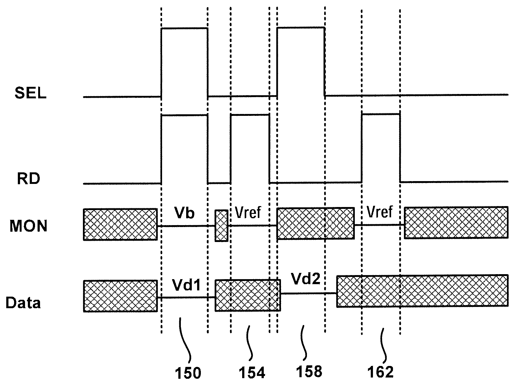
FIG. 2B is a timing diagram of first exemplary operation cycles for the pixel shown in FIG. 2A.
FIG. 2C is a timing diagram of second exemplary operation cycles for the pixel shown in FIG. 2A.
FIG. 3 is a circuit diagram of another exemplary pixel circuit configuration.
FIG. 4 is a block diagram of a modified configuration of a system for driving an OLED display using a shared readout circuit, while monitoring the degradation of the individual pixels and providing compensation therefor.
While the invention is susceptible to various modifications and alternative forms, specific embodiments have been shown by way of example in the drawings and will be described in detail herein. It should be understood, however, that the invention is not intended to be limited to the particular forms disclosed. Rather, the invention is to cover all modifications, equivalents, and alternatives falling within the spirit and scope of the invention as defined by the appended claims.
DETAILED DESCRIPTION
FIG. 1 is a diagram of an exemplary display system 50. The display system 50 includes an address driver 8, a data driver 4, a controller 2, a memory storage 6, and display panel 20. The display panel 20 includes an array of pixels 10 arranged in rows and columns. Each of the pixels 10 is individually programmable to emit light with individually programmable luminance values. The controller 2 receives digital data indicative of information to be displayed on the display panel 20. The controller 2 sends signals 32 to the data driver 4 and scheduling signals 34 to the address driver 8 to drive the pixels 10 in the display panel 20 to display the information indicated. The plurality of pixels 10 associated with the display panel 20 thus comprise a display array ("display screen") adapted to dynamically display information according to the input digital data received by the controller 2. The display screen can display, for example, video information from a stream of video data received by the controller 2. The supply voltage 14 can provide a constant power voltage or can be an adjustable voltage supply that is controlled by signals from the controller 2. The display system 50 can also incorporate features from a current source or sink (not shown) to provide biasing currents to the pixels 10 in the display panel 20 to thereby decrease programming time for the pixels 10.
For illustrative purposes, the display system 50 in FIG. 1 is illustrated with only four pixels 10 in the display panel 20. It is understood that the display system 50 can be implemented with a display screen that includes an array of similar pixels, such as the pixels 10, and that the display screen is not limited to a particular number of rows and columns of pixels. For example, the display system 50 can be implemented with a display screen with a number of rows and columns of pixels commonly available in displays for mobile devices, monitor-based devices, and/or projection-devices.
The pixel 10 is operated by a driving circuit ("pixel circuit") that generally includes a driving transistor and a light emitting device. Hereinafter the pixel 10 may refer to the pixel circuit. The light emitting device can optionally be an organic light emitting diode, but implementations of the present disclosure apply to pixel circuits having other electroluminescence devices, including current-driven light emitting devices. The driving transistor in the pixel 10 can optionally be an n-type or p-type amorphous silicon thin-film transistor, but implementations of the present disclosure are not limited to pixel circuits having a particular polarity of transistor or only to pixel circuits having thin-film transistors. The pixel circuit 10 can also include a storage capacitor for storing programming information and allowing the pixel circuit 10 to drive the light emitting device after being addressed. Thus, the display panel 20 can be an active matrix display array.
As illustrated in FIG. 1, the pixel 10 illustrated as the top-left pixel in the display panel 20 is coupled to a select line 24i, a supply line 26i, a data line 22j, and a monitor line 28j. A read line may also be included for controlling connections to the monitor line. In one implementation, the supply voltage 14 can also provide a second supply line to the pixel 10. For example, each pixel can be coupled to a first supply line 26 charged with Vdd and a second supply line 27 coupled with Vss, and the pixel circuits 10 can be situated between the first and second supply lines to facilitate driving current between the two supply lines during an emission phase of the pixel circuit. The top-left pixel 10 in the display panel 20 can correspond a pixel in the display panel in a "ith" row and "jth" column of the display panel 20. Similarly, the top-right pixel 10 in the display panel 20 represents a "jth" row and "mth" column; the bottom-left pixel 10 represents an "nth" row and "jth" column; and the bottom-right pixel 10 represents an "nth" row and "mth" column. Each of the pixels 10 is coupled to appropriate select lines (e.g., the select lines 24i and 24n), supply lines (e.g., the supply lines 26i and 26n), data lines (e.g., the data lines 22j and 22m), and monitor lines (e.g., the monitor lines 28j and 28m). It is noted that aspects of the present disclosure apply to pixels having additional connections, such as connections to additional select lines, and to pixels having fewer connections, such as pixels lacking a connection to a monitoring line.
With reference to the top-left pixel 10 shown in the display panel 20, the select line 24i is provided by the address driver 8, and can be utilized to enable, for example, a programming operation of the pixel 10 by activating a switch or transistor to allow the data line 22j to program the pixel 10. The data line 22j conveys programming information from the data driver 4 to the pixel 10. For example, the data line 22j can be utilized to apply a programming voltage or a programming current to the pixel 10 in order to program the pixel 10 to emit a desired amount of luminance. The programming voltage (or programming current) supplied by the data driver 4 via the data line 22j is a voltage (or current) appropriate to cause the pixel 10 to emit light with a desired amount of luminance according to the digital data received by the controller 2. The programming voltage (or programming current) can be applied to the pixel 10 during a programming operation of the pixel 10 so as to charge a storage device within the pixel 10, such as a storage capacitor, thereby enabling the pixel 10 to emit light with the desired amount of luminance during an emission operation following the programming operation. For example, the storage device in the pixel 10 can be charged during a programming operation to apply a voltage to one or more of a gate or a source terminal of the driving transistor during the emission operation, thereby causing the driving transistor to convey the driving current through the light emitting device according to the voltage stored on the storage device.
Generally, in the pixel 10, the driving current that is conveyed through the light emitting device by the driving transistor during the emission operation of the pixel 10 is a current that is supplied by the first supply line 26i and is drained to a second supply line 27i. The first supply line 26i and the second supply line 27i are coupled to the voltage supply 14. The first supply line 26i can provide a positive supply voltage (e.g., the voltage commonly referred to in circuit design as "Vdd") and the second supply line 27i can provide a negative supply voltage (e.g., the voltage commonly referred to in circuit design as "Vss"). Implementations of the present disclosure can be realized where one or the other of the supply lines (e.g., the supply line 27i) is fixed at a ground voltage or at another reference voltage.
The display system 50 also includes a monitoring system 12. With reference again to the top left pixel 10 in the display panel 20, the monitor line 28j connects the pixel 10 to the monitoring system 12. The monitoring system 12 can be integrated with the data driver 4, or can be a separate stand-alone system. In particular, the monitoring system 12 can optionally be implemented by monitoring the current and/or voltage of the data line 22j during a monitoring operation of the pixel 10, and the monitor line 28j can be entirely omitted. Additionally, the display system 50 can be implemented without the monitoring system 12 or the monitor line 28j. The monitor line 28j allows the monitoring system 12 to measure a current or voltage associated with the pixel 10 and thereby extract information indicative of a degradation of the pixel 10. For example, the monitoring system 12 can extract, via the monitor line 28j, a current flowing through the driving transistor within the pixel 10 and thereby determine, based on the measured current and based on the voltages applied to the driving transistor during the measurement, a threshold voltage of the driving transistor or a shift thereof.
The monitoring system 12 can also extract an operating voltage of the light emitting device (e.g., a voltage drop across the light emitting device while the light emitting device is operating to emit light). The monitoring system 12 can then communicate signals 32 to the controller 2 and/or the memory 6 to allow the display system 50 to store the extracted degradation information in the memory 6. During subsequent programming and/or emission operations of the pixel 10, the degradation information is retrieved from the memory 6 by the controller 2 via memory signals 36, and the controller 2 then compensates for the extracted degradation information in subsequent programming and/or emission operations of the pixel 10. For example, once the degradation information is extracted, the programming information conveyed to the pixel 10 via the data line 22j can be appropriately adjusted during a subsequent programming operation of the pixel 10 such that the pixel 10 emits light with a desired amount of luminance that is independent of the degradation of the pixel 10. In an example, an increase in the threshold voltage of the driving transistor within the pixel 10 can be compensated for by appropriately increasing the programming voltage applied to the pixel 10.
FIG. 2A is a circuit diagram of an exemplary driving circuit for a pixel 110. The driving circuit shown in FIG. 2A is utilized to calibrate, program and drive the pixel 110 and includes a drive transistor 112 for conveying a driving current through an organic light emitting diode ("OLED") 114. The OLED 114 emits light according to the current passing through the OLED 114, and can be replaced by any current-driven light emitting device. The OLED 114 has an inherent capacitance C.sub.OLED. The pixel 110 can be utilized in the display panel 20 of the display system 50 described in connection with FIG. 1.
The driving circuit for the pixel 110 also includes a storage capacitor 116 and a switching transistor 118. The pixel 110 is coupled to a select line SEL, a voltage supply line Vdd, a data line Vdata, and a monitor line MON. The driving transistor 112 draws a current from the voltage supply line Vdd according to a gate-source voltage (Vgs) across the gate and source terminals of the drive transistor 112. For example, in a saturation mode of the drive transistor 112, the current passing through the drive transistor 112 can be given by Ids=.beta.(Vgs-Vt).sup.2, where .beta. is a parameter that depends on device characteristics of the drive transistor 112, Ids is the current from the drain terminal to the source terminal of the drive transistor 112, and Vt is the threshold voltage of the drive transistor 112.
In the pixel 110, the storage capacitor 116 is coupled across the gate and source terminals of the drive transistor 112. The storage capacitor 116 has a first terminal, which is referred to for convenience as a gate-side terminal, and a second terminal, which is referred to for convenience as a source-side terminal. The gate-side terminal of the storage capacitor 116 is electrically coupled to the gate terminal of the drive transistor 112. The source-side terminal 116s of the storage capacitor 116 is electrically coupled to the source terminal of the drive transistor 112. Thus, the gate-source voltage Vgs of the drive transistor 112 is also the voltage charged on the storage capacitor 116. As will be explained further below, the storage capacitor 116 can thereby maintain a driving voltage across the drive transistor 112 during an emission phase of the pixel 110.
The drain terminal of the drive transistor 112 is connected to the voltage supply line Vdd, and the source terminal of the drive transistor 112 is connected to (1) the anode terminal of the OLED 114 and (2) a monitor line MON via a read transistor 119. A cathode terminal of the OLED 114 can be connected to ground or can optionally be connected to a second voltage supply line, such as the supply line Vss shown in FIG. 1. Thus, the OLED 114 is connected in series with the current path of the drive transistor 112. The OLED 114 emits light according to the magnitude of the current passing through the OLED 114, once a voltage drop across the anode and cathode terminals of the OLED achieves an operating voltage (V.sub.OLED) of the OLED 114. That is, when the difference between the voltage on the anode terminal and the voltage on the cathode terminal is greater than the operating voltage V.sub.OLED, the OLED 114 turns on and emits light. When the anode-to-cathode voltage is less than V.sub.OLED, current does not pass through the OLED 114.
The switching transistor 118 is operated according to the select line SEL (e.g., when the voltage on the select line SEL is at a high level, the switching transistor 118 is turned on, and when the voltage SEL is at a low level, the switching transistor is turned off). When turned on, the switching transistor 118 electrically couples node A (the gate terminal of the driving transistor 112 and the gate-side terminal of the storage capacitor 116) to the data line Vdata.
The read transistor 119 is operated according to the read line RD (e.g., when the voltage on the read line RD is at a high level, the read transistor 119 is turned on, and when the voltage RD is at a low level, the read transistor 119 is turned off). When turned on, the read transistor 119 electrically couples node B (the source terminal of the driving transistor 112, the source-side terminal of the storage capacitor 116, and the anode of the OLED 114) to the monitor line MON.
FIG. 2B is a timing diagram of exemplary operation cycles for the pixel 110 shown in FIG. 2A. During a first cycle 150, both the SEL line and the RD line are high, so the corresponding transistors 118 and 119 are turned on. The switching transistor 118 applies a voltage Vd1, which is at a level sufficient to turn on the drive transistor 112, from the data line Vdata to node A. The read transistor 119 applies a monitor-line voltage Vb, which is at a level that turns the OLED 114 off, from the monitor line MON to node B. As a result, the gate-source voltage Vgs is independent of V.sub.OLED (Vd1-Vb-Vds3, where Vds3 is the voltage drop across the read transistor 119). The SEL and RD lines go low at the end of the cycle 150, turning off the transistors 118 and 119.
During the second cycle 154, the SEL line is low to turn off the switching transistor 118, and the drive transistor 112 is turned on by the charge on the capacitor 116 at node A. The voltage on the read line RD goes high to turn on the read transistor 119 and thereby permit a first sample of the drive transistor current to be taken via the monitor line MON, while the OLED 114 is off. The voltage on the monitor line MON is Vref, which may be at the same level as the voltage Vb in the previous cycle.
During the third cycle 158, the voltage on the select line SEL is high to turn on the switching transistor 118, and the voltage on the read line RD is low to turn off the read transistor 119. Thus, the gate of the drive transistor 112 is charged to the voltage Vd2 of the data line Vdata, and the source of the drive transistor 112 is set to V.sub.OLED by the OLED 114. Consequently, the gate-source voltage Vgs of the drive transistor 112 is a function of V.sub.OLED (Vgs=Vd2-V.sub.OLED).
During the fourth cycle 162, the voltage on the select line SEL is low to turn off the switching transistor, and the drive transistor 112 is turned on by the charge on the capacitor 116 at node A. The voltage on the read line RD is high to turn on the read transistor 119, and a second sample of the current of the drive transistor 112 is taken via the monitor line MON.
If the first and second samples of the drive current are not the same, the voltage Vd2 on the Vdata line is adjusted, the programming voltage Vd2 is changed, and the sampling and adjustment operations are repeated until the second sample of the drive current is the same as the first sample. When the two samples of the drive current are the same, the two gate-source voltages should also be the same, which means that:
.times..times..times..times..times..times..times..times..times..times..ti- mes..times..times..times..times..times..times. ##EQU00001##
After some operation time (t), the change in V.sub.OLED between time 0 and time t is .DELTA.V.sub.OLED=V.sub.OLED(t)-V.sub.OLED(0)=Vd2(t)-Vd2(0). Thus, the difference between the two programming voltages Vd2(t) and Vd2(0) can be used to extract the OLED voltage.
FIG. 2C is a modified schematic timing diagram of another set of exemplary operation cycles for the pixel 110 shown in FIG. 2A, for taking only a single reading of the drive current and comparing that value with a known reference value. For example, the reference value can be the desired value of the drive current derived by the controller to compensate for degradation of the drive transistor 112 as it ages. The OLED voltage V.sub.OLED can be extracted by measuring the difference between the pixel currents when the pixel is programmed with fixed voltages in both methods (being affected by V.sub.OLED and not being affected by V.sub.OLED). This difference and the current-voltage characteristics of the pixel can then be used to extract V.sub.OLED.
During the first cycle 200 of the exemplary timing diagram in FIG. 2C, the select line SEL is high to turn on the switching transistor 118, and the read line RD is low to turn off the read transistor 118. The data line Vdata supplies a voltage Vd2 to node A via the switching transistor 118. During the second cycle 201, SEL is low to turn off the switching transistor 118, and RD is high to turn on the read transistor 119. The monitor line MON supplies a voltage Vref to the node B via the read transistor 118, while a reading of the value of the drive current is taken via the read transistor 119 and the monitor line MON. This read value is compared with the known reference value of the drive current and, if the read value and the reference value of the drive current are different, the cycles 200 and 201 are repeated using an adjusted value of the voltage Vd2. This process is repeated until the read value and the reference value of the drive current are substantially the same, and then the adjusted value of Vd2 can be used to determine V.sub.OLED.
FIG. 3 is a circuit diagram of two of the pixels 110a and 110b like those shown in FIG. 2A but modified to share a common monitor line MON, while still permitting independent measurement of the driving current and OLED voltage separately for each pixel. The two pixels 110a and 110b are in the same row but in different columns, and the two columns share the same monitor line MON. Only the pixel selected for measurement is programmed with valid voltages, while the other pixel is programmed to turn off the drive transistor 12 during the measurement cycle. Thus, the drive transistor of one pixel will have no effect on the current measurement in the other pixel.
FIG. 4 illustrates a modified drive system that utilizes a readout circuit 300 that is shared by multiple columns of pixels while still permitting the measurement of the driving current and OLED voltage independently for each of the individual pixels 10. Although only four columns are illustrated in FIG. 4, it will be understood that a typical display contains a much larger number of columns, and they can all use the same readout circuit. Alternatively, multiple readout circuits can be utilized, with each readout circuit still sharing multiple columns, so that the number of readout circuits is significantly less than the number of columns. Only the pixel selected for measurement at any given time is programmed with valid voltages, while all the other pixels sharing the same gate signals are programmed with voltages that cause the respective drive transistors to be off. Consequently, the drive transistors of the other pixels will have no effect on the current measurement being taken of the selected pixel. Also, when the driving current in the selected pixel is used to measure the OLED voltage, the measurement of the OLED voltage is also independent of the drive transistors of the other pixels.
While particular embodiments and applications of the present invention have been illustrated and described, it is to be understood that the invention is not limited to the precise construction and compositions disclosed herein and that various modifications, changes, and variations can be apparent from the foregoing descriptions without departing from the spirit and scope of the invention as defined in the appended claims.
* * * * *
uspto.report is an independent third-party trademark research tool that is not affiliated, endorsed, or sponsored by the United States Patent and Trademark Office (USPTO) or any other governmental organization. The information provided by uspto.report is based on publicly available data at the time of writing and is intended for informational purposes only.
While we strive to provide accurate and up-to-date information, we do not guarantee the accuracy, completeness, reliability, or suitability of the information displayed on this site. The use of this site is at your own risk. Any reliance you place on such information is therefore strictly at your own risk.
All official trademark data, including owner information, should be verified by visiting the official USPTO website at www.uspto.gov. This site is not intended to replace professional legal advice and should not be used as a substitute for consulting with a legal professional who is knowledgeable about trademark law.