Pixel circuits for mitigation of hysteresis
Chaji , et al.
U.S. patent number 10,586,491 [Application Number 15/832,962] was granted by the patent office on 2020-03-10 for pixel circuits for mitigation of hysteresis. This patent grant is currently assigned to Ignis Innovation Inc.. The grantee listed for this patent is Ignis Innovation Inc.. Invention is credited to Yaser Azizi, Gholamreza Chaji.


| United States Patent | 10,586,491 |
| Chaji , et al. | March 10, 2020 |
Pixel circuits for mitigation of hysteresis
Abstract
What is disclosed are display systems and methods of compensation of images produced by active matrix light emitting diode device (AMOLED) and other emissive displays. Anomalies in luminance produced by pixel circuits due to hysteresis effects are corrected through in-pixel compensation and resetting of the driving transistor.
| Inventors: | Chaji; Gholamreza (Waterloo, CA), Azizi; Yaser (Waterloo, CA) | ||||||||||
|---|---|---|---|---|---|---|---|---|---|---|---|
| Applicant: |
|
||||||||||
| Assignee: | Ignis Innovation Inc.
(Waterloo, CA) |
||||||||||
| Family ID: | 62164303 | ||||||||||
| Appl. No.: | 15/832,962 | ||||||||||
| Filed: | December 6, 2017 |
Prior Publication Data
| Document Identifier | Publication Date | |
|---|---|---|
| US 20180158415 A1 | Jun 7, 2018 | |
Related U.S. Patent Documents
| Application Number | Filing Date | Patent Number | Issue Date | ||
|---|---|---|---|---|---|
| 62430437 | Dec 6, 2016 | ||||
| Current U.S. Class: | 1/1 |
| Current CPC Class: | G09G 3/3258 (20130101); G09G 3/3233 (20130101); G09G 2310/0262 (20130101); G09G 2320/0295 (20130101); G09G 2320/0693 (20130101); G09G 2300/0861 (20130101); G09G 2310/0251 (20130101); G09G 2320/0209 (20130101) |
| Current International Class: | G09G 3/3258 (20160101); G09G 3/3233 (20160101) |
References Cited [Referenced By]
U.S. Patent Documents
| 4354162 | October 1982 | Wright |
| 4758831 | July 1988 | Kasahara et al. |
| 4963860 | October 1990 | Stewart |
| 4975691 | December 1990 | Lee |
| 4996523 | February 1991 | Bell et al. |
| 5051739 | September 1991 | Hayashida et al. |
| 5222082 | June 1993 | Plus |
| 5266515 | November 1993 | Robb et al. |
| 5498880 | March 1996 | Lee et al. |
| 5589847 | December 1996 | Lewis |
| 5619033 | April 1997 | Weisfield |
| 5648276 | July 1997 | Hara et al. |
| 5670973 | September 1997 | Bassetti et al. |
| 5684365 | November 1997 | Tang et al. |
| 5686935 | November 1997 | Weisbrod |
| 5712653 | January 1998 | Katoh et al. |
| 5714968 | February 1998 | Ikeda |
| 5747928 | May 1998 | Shanks et al. |
| 5748160 | May 1998 | Shieh et al. |
| 5784042 | July 1998 | Ono et al. |
| 5790234 | August 1998 | Matsuyama |
| 5815303 | September 1998 | Berlin |
| 5870071 | February 1999 | Kawahata |
| 5874803 | February 1999 | Garbuzov et al. |
| 5880582 | March 1999 | Sawada |
| 5903248 | May 1999 | Irwin |
| 5917280 | June 1999 | Burrows et al. |
| 5923794 | July 1999 | McGrath et al. |
| 5952789 | September 1999 | Stewart et al. |
| 5990629 | November 1999 | Yamada et al. |
| 6023259 | February 2000 | Howard et al. |
| 6069365 | May 2000 | Chow et al. |
| 6081131 | June 2000 | Ishii |
| 6091203 | July 2000 | Kawashima et al. |
| 6097360 | August 2000 | Holloman |
| 6144222 | November 2000 | Ho |
| 6157583 | December 2000 | Starnes et al. |
| 6166489 | December 2000 | Thompson et al. |
| 6177915 | January 2001 | Beeteson et al. |
| 6225846 | May 2001 | Wada et al. |
| 6229508 | May 2001 | Kane |
| 6232939 | May 2001 | Saito et al. |
| 6246180 | June 2001 | Nishigaki |
| 6252248 | June 2001 | Sano et al. |
| 6259424 | July 2001 | Kurogane |
| 6274887 | August 2001 | Yamazaki et al. |
| 6288696 | September 2001 | Holloman |
| 6300928 | October 2001 | Kim |
| 6303963 | October 2001 | Ohtani et al. |
| 6306694 | October 2001 | Yamazaki et al. |
| 6307322 | October 2001 | Dawson et al. |
| 6316786 | November 2001 | Mueller et al. |
| 6320325 | November 2001 | Cok et al. |
| 6323631 | November 2001 | Juang |
| 6323832 | November 2001 | Nishizawa et al. |
| 6345085 | February 2002 | Yeo et al. |
| 6348835 | February 2002 | Sato et al. |
| 6365917 | April 2002 | Yamazaki |
| 6373453 | April 2002 | Yudasaka |
| 6384427 | May 2002 | Yamazaki et al. |
| 6392617 | May 2002 | Gleason |
| 6399988 | June 2002 | Yamazaki |
| 6414661 | July 2002 | Shen et al. |
| 6420758 | July 2002 | Nakajima |
| 6420834 | July 2002 | Yamazaki et al. |
| 6420988 | July 2002 | Azami et al. |
| 6433488 | August 2002 | Bu |
| 6445376 | September 2002 | Parrish |
| 6468638 | October 2002 | Jacobsen et al. |
| 6489952 | December 2002 | Tanaka et al. |
| 6501098 | December 2002 | Yamazaki |
| 6501466 | December 2002 | Yamagashi et al. |
| 6512271 | January 2003 | Yamazaki et al. |
| 6518594 | February 2003 | Nakajima et al. |
| 6524895 | February 2003 | Yamazaki et al. |
| 6531713 | March 2003 | Yamazaki |
| 6559594 | May 2003 | Fukunaga et al. |
| 6573195 | June 2003 | Yamazaki et al. |
| 6573584 | June 2003 | Nagakari et al. |
| 6576926 | June 2003 | Yamazaki et al. |
| 6577302 | June 2003 | Hunter |
| 6580408 | June 2003 | Bae et al. |
| 6580657 | June 2003 | Sanford et al. |
| 6583775 | June 2003 | Sekiya et al. |
| 6583776 | June 2003 | Yamazaki et al. |
| 6587086 | July 2003 | Koyama |
| 6593691 | July 2003 | Nishi et al. |
| 6594606 | July 2003 | Everitt |
| 6597203 | July 2003 | Forbes |
| 6611108 | August 2003 | Kimura |
| 6617644 | September 2003 | Yamazaki et al. |
| 6618030 | September 2003 | Kane et al. |
| 6641933 | November 2003 | Yamazaki et al. |
| 6661180 | December 2003 | Koyama |
| 6661397 | December 2003 | Mikami et al. |
| 6670637 | December 2003 | Yamazaki et al. |
| 6677713 | January 2004 | Sung |
| 6680577 | January 2004 | Inukai et al. |
| 6687266 | February 2004 | Ma et al. |
| 6690344 | February 2004 | Takeuchi et al. |
| 6693388 | February 2004 | Oomura |
| 6693610 | February 2004 | Shannon et al. |
| 6697057 | February 2004 | Koyama et al. |
| 6720942 | April 2004 | Lee et al. |
| 6734636 | May 2004 | Sanford et al. |
| 6738034 | May 2004 | Kaneko et al. |
| 6738035 | May 2004 | Fan |
| 6771028 | August 2004 | Winters |
| 6777712 | August 2004 | Sanford et al. |
| 6780687 | August 2004 | Nakajima et al. |
| 6806638 | October 2004 | Lih et al. |
| 6806857 | October 2004 | Sempel et al. |
| 6809706 | October 2004 | Shimoda |
| 6859193 | February 2005 | Yumoto |
| 6861670 | March 2005 | Ohtani et al. |
| 6873117 | March 2005 | Ishizuka |
| 6873320 | March 2005 | Nakamura |
| 6878968 | April 2005 | Ohnuma |
| 6909114 | June 2005 | Yamazaki |
| 6909419 | June 2005 | Zavracky et al. |
| 6919871 | July 2005 | Kwon |
| 6937215 | August 2005 | Lo |
| 6940214 | September 2005 | Komiya et al. |
| 6943500 | September 2005 | LeChevalier |
| 6954194 | October 2005 | Matsumoto et al. |
| 6956547 | October 2005 | Bae et al. |
| 6995510 | February 2006 | Murakami et al. |
| 6995519 | February 2006 | Arnold et al. |
| 7022556 | April 2006 | Adachi |
| 7023408 | April 2006 | Chen et al. |
| 7027015 | April 2006 | Booth, Jr. et al. |
| 7034793 | April 2006 | Sekiya et al. |
| 7088051 | August 2006 | Cok |
| 7106285 | September 2006 | Naugler |
| 7116058 | October 2006 | Lo et al. |
| 7129914 | October 2006 | Knapp et al. |
| 7129917 | October 2006 | Yamazaki et al. |
| 7141821 | November 2006 | Yamazaki et al. |
| 7161566 | January 2007 | Cok et al. |
| 7193589 | March 2007 | Yoshida et al. |
| 7199516 | April 2007 | Seo et al. |
| 7220997 | May 2007 | Nakata |
| 7235810 | June 2007 | Yamazaki et al. |
| 7245277 | July 2007 | Ishizuka |
| 7248236 | July 2007 | Nathan et al. |
| 7264979 | September 2007 | Yamagata et al. |
| 7274345 | September 2007 | Imamura et al. |
| 7274363 | September 2007 | Ishizuka et al. |
| 7279711 | October 2007 | Yamazaki et al. |
| 7304621 | December 2007 | Oomori et al. |
| 7310092 | December 2007 | Imamura |
| 7315295 | January 2008 | Kimura |
| 7317429 | January 2008 | Shirasaki et al. |
| 7319465 | January 2008 | Mikami et al. |
| 7321348 | January 2008 | Cok et al. |
| 7339636 | March 2008 | Voloschenko et al. |
| 7355574 | April 2008 | Leon et al. |
| 7358941 | April 2008 | Ono et al. |
| 7402467 | July 2008 | Kadono et al. |
| 7414600 | August 2008 | Nathan et al. |
| 7432885 | October 2008 | Asano et al. |
| 7474285 | January 2009 | Kimura |
| 7485478 | February 2009 | Yamagata et al. |
| 7502000 | March 2009 | Yuki et al. |
| 7535449 | May 2009 | Miyazawa |
| 7554512 | June 2009 | Steer |
| 7569849 | August 2009 | Nathan et al. |
| 7619594 | November 2009 | Hu |
| 7619597 | November 2009 | Nathan et al. |
| 7697052 | April 2010 | Yamazaki et al. |
| 7825419 | November 2010 | Yamagata et al. |
| 7859492 | December 2010 | Kohno |
| 7868859 | January 2011 | Tomida et al. |
| 7876294 | January 2011 | Sasaki et al. |
| 7948170 | May 2011 | Striakhilev et al. |
| 7948456 | May 2011 | Yamashita |
| 7969390 | June 2011 | Yoshida |
| 7995010 | August 2011 | Yamazaki et al. |
| 8044893 | October 2011 | Nathan et al. |
| 8115707 | February 2012 | Nathan et al. |
| 8378362 | February 2013 | Heo et al. |
| 8493295 | July 2013 | Yamazaki et al. |
| 8497525 | July 2013 | Yamagata et al. |
| 9385169 | July 2016 | Chaji et al. |
| 9606607 | March 2017 | Chaji |
| 9633597 | April 2017 | Nathan et al. |
| 9728135 | August 2017 | Nathan et al. |
| 9741292 | August 2017 | Nathan et al. |
| 2001/0002703 | June 2001 | Koyama |
| 2001/0004190 | June 2001 | Nishi et al. |
| 2001/0013806 | August 2001 | Notani |
| 2001/0015653 | August 2001 | De Jong et al. |
| 2001/0020926 | September 2001 | Kujik |
| 2001/0024186 | September 2001 | Kane |
| 2001/0026127 | October 2001 | Yoneda et al. |
| 2001/0026179 | October 2001 | Saeki |
| 2001/0026257 | October 2001 | Kimura |
| 2001/0030323 | October 2001 | Ikeda |
| 2001/0033199 | October 2001 | Aoki |
| 2001/0038098 | November 2001 | Yamazaki et al. |
| 2001/0043173 | November 2001 | Troutman |
| 2001/0045929 | November 2001 | Prache et al. |
| 2001/0052006 | December 2001 | Sempel et al. |
| 2001/0052898 | December 2001 | Osame et al. |
| 2002/0000576 | January 2002 | Inukai |
| 2002/0011796 | January 2002 | Koyama |
| 2002/0011799 | January 2002 | Kimura |
| 2002/0011981 | January 2002 | Kujik |
| 2002/0015031 | February 2002 | Fujita et al. |
| 2002/0015032 | February 2002 | Koyama et al. |
| 2002/0030528 | March 2002 | Matsumoto et al. |
| 2002/0030647 | March 2002 | Hack et al. |
| 2002/0036463 | March 2002 | Yoneda et al. |
| 2002/0047852 | April 2002 | Inukai et al. |
| 2002/0048829 | April 2002 | Yamazaki et al. |
| 2002/0050795 | May 2002 | Imura |
| 2002/0053401 | May 2002 | Ishikawa et al. |
| 2002/0070909 | June 2002 | Asano et al. |
| 2002/0080108 | June 2002 | Wang |
| 2002/0084463 | July 2002 | Sanford et al. |
| 2002/0101172 | August 2002 | Bu |
| 2002/0101433 | August 2002 | McKnight |
| 2002/0113248 | August 2002 | Yamagata et al. |
| 2002/0122308 | September 2002 | Ikeda |
| 2002/0130686 | September 2002 | Forbes |
| 2002/0154084 | October 2002 | Tanaka et al. |
| 2002/0158823 | October 2002 | Zavracky et al. |
| 2002/0163314 | November 2002 | Yamazaki et al. |
| 2002/0167471 | November 2002 | Everitt |
| 2002/0180369 | December 2002 | Koyama |
| 2002/0180721 | December 2002 | Kimura et al. |
| 2002/0186214 | December 2002 | Siwinski |
| 2002/0190332 | December 2002 | Lee et al. |
| 2002/0190924 | December 2002 | Asano et al. |
| 2002/0190971 | December 2002 | Nakamura et al. |
| 2002/0195967 | December 2002 | Kim et al. |
| 2002/0195968 | December 2002 | Sanford et al. |
| 2003/0020413 | January 2003 | Oomura |
| 2003/0030603 | February 2003 | Shimoda |
| 2003/0062524 | April 2003 | Kimura |
| 2003/0063081 | April 2003 | Kimura et al. |
| 2003/0071804 | April 2003 | Yamazaki et al. |
| 2003/0071821 | April 2003 | Sundahl |
| 2003/0076048 | April 2003 | Rutherford |
| 2003/0090445 | May 2003 | Chen et al. |
| 2003/0090447 | May 2003 | Kimura |
| 2003/0090481 | May 2003 | Kimura |
| 2003/0095087 | May 2003 | Libsch |
| 2003/0107560 | June 2003 | Yumoto et al. |
| 2003/0111966 | June 2003 | Mikami et al. |
| 2003/0122745 | July 2003 | Miyazawa |
| 2003/0140958 | July 2003 | Yang et al. |
| 2003/0151569 | August 2003 | Lee et al. |
| 2003/0169219 | September 2003 | LeChevalier |
| 2003/0174152 | September 2003 | Noguchi |
| 2003/0178617 | September 2003 | Appenzeller et al. |
| 2003/0179626 | September 2003 | Sanford et al. |
| 2003/0197663 | October 2003 | Lee et al. |
| 2003/0206060 | November 2003 | Suzuki |
| 2003/0230980 | December 2003 | Forrest et al. |
| 2004/0027063 | February 2004 | Nishikawa |
| 2004/0056604 | March 2004 | Shih et al. |
| 2004/0066357 | April 2004 | Kawasaki |
| 2004/0070557 | April 2004 | Asano et al. |
| 2004/0080262 | April 2004 | Park et al. |
| 2004/0080470 | April 2004 | Yamazaki et al. |
| 2004/0090400 | May 2004 | Yoo |
| 2004/0108518 | June 2004 | Jo |
| 2004/0113903 | June 2004 | Mikami et al. |
| 2004/0129933 | July 2004 | Nathan et al. |
| 2004/0130516 | July 2004 | Nathan et al. |
| 2004/0135749 | July 2004 | Kondakov et al. |
| 2004/0145547 | July 2004 | Oh |
| 2004/0150592 | August 2004 | Mizukoshi et al. |
| 2004/0150594 | August 2004 | Koyama et al. |
| 2004/0150595 | August 2004 | Kasai |
| 2004/0155841 | August 2004 | Kasai |
| 2004/0174347 | September 2004 | Sun et al. |
| 2004/0174349 | September 2004 | Libsch |
| 2004/0183759 | September 2004 | Stevenson et al. |
| 2004/0189627 | September 2004 | Shirasaki et al. |
| 2004/0196275 | October 2004 | Hattori |
| 2004/0201554 | October 2004 | Satoh |
| 2004/0207615 | October 2004 | Yumoto |
| 2004/0233125 | November 2004 | Tanghe et al. |
| 2004/0239596 | December 2004 | Ono et al. |
| 2004/0252089 | December 2004 | Ono et al. |
| 2004/0257355 | December 2004 | Naugler |
| 2004/0263437 | December 2004 | Hattori |
| 2005/0007357 | January 2005 | Yamashita et al. |
| 2005/0030267 | February 2005 | Tanghe et al. |
| 2005/0035709 | February 2005 | Furuie et al. |
| 2005/0067970 | March 2005 | Libsch et al. |
| 2005/0067971 | March 2005 | Kane |
| 2005/0068270 | March 2005 | Awakura |
| 2005/0088085 | April 2005 | Nishikawa et al. |
| 2005/0088103 | April 2005 | Kageyama et al. |
| 2005/0110420 | May 2005 | Arnold et al. |
| 2005/0117096 | June 2005 | Voloschenko et al. |
| 2005/0140598 | June 2005 | Kim et al. |
| 2005/0140610 | June 2005 | Smith et al. |
| 2005/0145891 | July 2005 | Abe |
| 2005/0156831 | July 2005 | Yamazaki et al. |
| 2005/0168416 | August 2005 | Hashimoto et al. |
| 2005/0206590 | September 2005 | Sasaki et al. |
| 2005/0225686 | October 2005 | Brummack et al. |
| 2005/0260777 | November 2005 | Brabec et al. |
| 2005/0269959 | December 2005 | Uchino et al. |
| 2005/0269960 | December 2005 | Ono et al. |
| 2005/0285822 | December 2005 | Reddy et al. |
| 2005/0285825 | December 2005 | Eom et al. |
| 2006/0007072 | January 2006 | Choi et al. |
| 2006/0012310 | January 2006 | Chen et al. |
| 2006/0027807 | February 2006 | Nathan et al. |
| 2006/0030084 | February 2006 | Young |
| 2006/0038758 | February 2006 | Routley et al. |
| 2006/0044227 | March 2006 | Hadcock |
| 2006/0066527 | March 2006 | Chou |
| 2006/0092185 | May 2006 | Jo et al. |
| 2006/0232522 | October 2006 | Roy et al. |
| 2006/0261841 | November 2006 | Fish |
| 2006/0264143 | November 2006 | Lee et al. |
| 2006/0273997 | December 2006 | Nathan et al. |
| 2006/0284801 | December 2006 | Yoon et al. |
| 2007/0001937 | January 2007 | Park et al. |
| 2007/0001939 | January 2007 | Hashimoto et al. |
| 2007/0008268 | January 2007 | Park et al. |
| 2007/0008297 | January 2007 | Bassetti |
| 2007/0046195 | March 2007 | Chin et al. |
| 2007/0069998 | March 2007 | Naugler et al. |
| 2007/0080905 | April 2007 | Takahara |
| 2007/0080906 | April 2007 | Tanabe |
| 2007/0080908 | April 2007 | Nathan et al. |
| 2007/0080918 | April 2007 | Kawachi et al. |
| 2007/0103419 | May 2007 | Uchino et al. |
| 2007/0182671 | August 2007 | Nathan et al. |
| 2007/0273294 | November 2007 | Nagayama |
| 2007/0285359 | December 2007 | Ono |
| 2007/0296672 | December 2007 | Kim et al. |
| 2008/0012835 | January 2008 | Rimon et al. |
| 2008/0042948 | February 2008 | Yamashita et al. |
| 2008/0055209 | March 2008 | Cok |
| 2008/0074413 | March 2008 | Ogura |
| 2008/0088549 | April 2008 | Nathan et al. |
| 2008/0122803 | May 2008 | Izadi et al. |
| 2008/0230118 | September 2008 | Nakatani et al. |
| 2009/0032807 | February 2009 | Shinohara et al. |
| 2009/0051283 | February 2009 | Cok et al. |
| 2009/0160743 | June 2009 | Tomida et al. |
| 2009/0162961 | June 2009 | Deane |
| 2009/0174628 | July 2009 | Wang et al. |
| 2009/0179838 | July 2009 | Yamashita |
| 2009/0213046 | August 2009 | Nam |
| 2010/0039422 | February 2010 | Seto |
| 2010/0052524 | March 2010 | Kinoshita |
| 2010/0078230 | April 2010 | Rosenblatt et al. |
| 2010/0079711 | April 2010 | Tanaka |
| 2010/0097335 | April 2010 | Jung et al. |
| 2010/0133994 | June 2010 | Song et al. |
| 2010/0134456 | June 2010 | Oyamada |
| 2010/0140600 | June 2010 | Clough et al. |
| 2010/0156279 | June 2010 | Tamura et al. |
| 2010/0237374 | September 2010 | Chu et al. |
| 2010/0328294 | December 2010 | Sasaki et al. |
| 2011/0090210 | April 2011 | Sasaki et al. |
| 2011/0133636 | June 2011 | Matsuo et al. |
| 2011/0148801 | June 2011 | Bateman et al. |
| 2011/0180825 | July 2011 | Lee et al. |
| 2012/0212468 | August 2012 | Govil |
| 2013/0009930 | January 2013 | Cho et al. |
| 2013/0032831 | February 2013 | Chaji et al. |
| 2013/0113785 | May 2013 | Sumi |
| 1294034 | Jan 1992 | CA | |||
| 2109951 | Nov 1992 | CA | |||
| 2 249 592 | Jul 1998 | CA | |||
| 2 368 386 | Sep 1999 | CA | |||
| 2 242 720 | Jan 2000 | CA | |||
| 2 354 018 | Jun 2000 | CA | |||
| 2 436 451 | Aug 2002 | CA | |||
| 2 438 577 | Aug 2002 | CA | |||
| 2 483 645 | Dec 2003 | CA | |||
| 2 463 653 | Jan 2004 | CA | |||
| 2498136 | Mar 2004 | CA | |||
| 2522396 | Nov 2004 | CA | |||
| 2443206 | Mar 2005 | CA | |||
| 2472671 | Dec 2005 | CA | |||
| 2567076 | Jan 2006 | CA | |||
| 2526782 | Apr 2006 | CA | |||
| 1381032 | Nov 2002 | CN | |||
| 1448908 | Oct 2003 | CN | |||
| 1776922 | May 2006 | CN | |||
| 101032027 | Sep 2007 | CN | |||
| 101256293 | Sep 2008 | CN | |||
| 101727237 | Jun 2010 | CN | |||
| 102799331 | Nov 2012 | CN | |||
| 102955600 | Mar 2013 | CN | |||
| 20 2006 005427 | Jun 2006 | DE | |||
| 0 940 796 | Sep 1999 | EP | |||
| 1 028 471 | Aug 2000 | EP | |||
| 1 103 947 | May 2001 | EP | |||
| 1 130 565 | Sep 2001 | EP | |||
| 1 184 833 | Mar 2002 | EP | |||
| 1 194 013 | Apr 2002 | EP | |||
| 1 310 939 | May 2003 | EP | |||
| 1 335 430 | Aug 2003 | EP | |||
| 1 372 136 | Dec 2003 | EP | |||
| 1 381 019 | Jan 2004 | EP | |||
| 1 418 566 | May 2004 | EP | |||
| 1 429 312 | Jun 2004 | EP | |||
| 1 439 520 | Jul 2004 | EP | |||
| 1 465 143 | Oct 2004 | EP | |||
| 1 467 408 | Oct 2004 | EP | |||
| 1 517 290 | Mar 2005 | EP | |||
| 1 521 203 | Apr 2005 | EP | |||
| 2317499 | May 2011 | EP | |||
| 2 205 431 | Dec 1988 | GB | |||
| 09 090405 | Apr 1997 | JP | |||
| 10-153759 | Jun 1998 | JP | |||
| 10-254410 | Sep 1998 | JP | |||
| 11 231805 | Aug 1999 | JP | |||
| 11-282419 | Oct 1999 | JP | |||
| 2000/056847 | Feb 2000 | JP | |||
| 2000-077192 | Mar 2000 | JP | |||
| 2000-089198 | Mar 2000 | JP | |||
| 2000-352941 | Dec 2000 | JP | |||
| 2002-91376 | Mar 2002 | JP | |||
| 2002-268576 | Sep 2002 | JP | |||
| 2002-278513 | Sep 2002 | JP | |||
| 2002-333862 | Nov 2002 | JP | |||
| 2003-022035 | Jan 2003 | JP | |||
| 2003-076331 | Mar 2003 | JP | |||
| 2003-150082 | May 2003 | JP | |||
| 2003-177709 | Jun 2003 | JP | |||
| 2003-271095 | Sep 2003 | JP | |||
| 2003-308046 | Oct 2003 | JP | |||
| 2005-057217 | Mar 2005 | JP | |||
| 2006065148 | Mar 2006 | JP | |||
| 2009282158 | Dec 2009 | JP | |||
| 485337 | May 2002 | TW | |||
| 502233 | Sep 2002 | TW | |||
| 538650 | Jun 2003 | TW | |||
| 569173 | Jan 2004 | TW | |||
| WO 94/25954 | Nov 1994 | WO | |||
| WO 99/48079 | Sep 1999 | WO | |||
| WO 01/27910 | Apr 2001 | WO | |||
| WO 02/067327 | Aug 2002 | WO | |||
| WO 03/034389 | Apr 2003 | WO | |||
| WO 03/063124 | Jul 2003 | WO | |||
| WO 03/077231 | Sep 2003 | WO | |||
| WO 03/105117 | Dec 2003 | WO | |||
| WO 2004/003877 | Jan 2004 | WO | |||
| WO 2004/034364 | Apr 2004 | WO | |||
| WO 2005/022498 | Mar 2005 | WO | |||
| WO 2005/029455 | Mar 2005 | WO | |||
| WO 2005/055185 | Jun 2005 | WO | |||
| WO 2006/053424 | May 2006 | WO | |||
| WO 2006/063448 | Jun 2006 | WO | |||
| WO 2006/137337 | Dec 2006 | WO | |||
| WO 2007/003877 | Jan 2007 | WO | |||
| WO 2007/079572 | Jul 2007 | WO | |||
| WO 2010/023270 | Mar 2010 | WO | |||
Other References
|
Ahnood et al.: "Effect of threshold voltage instability on field effect mobility in thin film transistors deduced from constant current measurements"; dated Aug. 2009 (3 pages). cited by applicant . Alexander et al.: "Pixel circuits and drive schemes for glass and elastic AMOLED displays"; dated Jul. 2005 (9 pages). cited by applicant . Alexander et al.: "Unique Electrical Measurement Technology for Compensation, Inspection, and Process Diagnostics of AMOLED HDTV"; dated May 2010 (4 pages). cited by applicant . Ashtiani et al.: "AMOLED Pixel Circuit With Electronic Compensation of Luminance Degradation"; dated Mar. 2007 (4 pages). cited by applicant . Chaji et al.: "A Current-Mode Comparator for Digital Calibration of Amorphous Silicon AMOLED Displays"; dated Jul. 2008 (5 pages). cited by applicant . Chaji et al.: "A fast settling current driver based on the CCII for AMOLED displays"; dated Dec. 2009 (6 pages). cited by applicant . Chaji et al.: "A Low-Cost Stable Amorphous Silicon AMOLED Display with Full V.about.T- and V.about.O.about.L.about.E.about.D Shift Compensation"; dated May 2007 (4 pages). cited by applicant . Chaji et al.: "A low-power driving scheme for a-Si:H active-matrix organic light-emitting diode displays"; dated Jun. 2005 (4 pages). cited by applicant . Chaji et al.: "A low-power high-performance digital circuit for deep submicron technologies"; dated Jun. 2005 (4 pages). cited by applicant . Chaji et al.: "A novel a-Si:H AMOLED pixel circuit based on short-term stress stability of a-Si:H TFTs"; dated Oct. 2005 (3 pages). cited by applicant . Chaji et al.: "A Novel Driving Scheme and Pixel Circuit for AMOLED Displays"; dated Jun. 2006 (4 pages). cited by applicant . Chaji et al.: "A novel driving scheme for high-resolution large-area a-Si:H AMOLED displays"; dated Aug. 2005 (4 pages). cited by applicant . Chaji et al.: "A Stable Voltage-Programmed Pixel Circuit for a-Si:H AMOLED Displays"; dated Dec. 2006 (12 pages). cited by applicant . Chaji et al.: "A Sub-.mu.A fast-settling current-programmed pixel circuit for AMOLED displays"; dated Sep. 2007. cited by applicant . Chaji et al.: "An Enhanced and Simplified Optical Feedback Pixel Circuit for AMOLED Displays"; dated Oct. 2006. cited by applicant . Chaji et al.: "Compensation technique for DC and transient instability of thin film transistor circuits for large-area devices"; dated Aug. 2008. cited by applicant . Chaji et al.: "Driving scheme for stable operation of 2-TFT a-Si AMOLED pixel"; dated Apr. 2005 (2 pages). cited by applicant . Chaji et al.: "Dynamic-effect compensating technique for stable a-Si:H AMOLED displays"; dated Aug. 2005 (4 pages). cited by applicant . Chaji et al.: "Electrical Compensation of OLED Luminance Degradation"; dated Dec. 2007 (3 pages). cited by applicant . Chaji et al.: "eUTDSP: a design study of a new VLIW-based DSP architecture"; dated My 2003 (4 pages). cited by applicant . Chaji et al.: "Fast and Offset-Leakage Insensitive Current-Mode Line Driver for Active Matrix Displays and Sensors"; dated Feb. 2009 (8 pages). cited by applicant . Chaji et al.: "High Speed Low Power Adder Design With a New Logic Style: Pseudo Dynamic Logic (SDL)"; dated Oct. 2001 (4 pages). cited by applicant . Chaji et al.: "High-precision, fast current source for large-area current-programmed a-Si flat panels"; dated Sep. 2006 (4 pages). cited by applicant . Chaji et al.: "Low-Cost AMOLED Television with IGNIS Compensating Technology"; dated May 2008 (4 pages). cited by applicant . Chaji et al.: "Low-Cost Stable a-Si:H AMOLED Display for Portable Applications"; dated Jun. 2006 (4 pages). cited by applicant . Chaji et al.: "Low-Power Low-Cost Voltage-Programmed a-Si:H AMOLED Display"; dated Jun. 2008 (5 pages). cited by applicant . Chaji et al.: "Merged phototransistor pixel with enhanced near infrared response and flicker noise reduction for biomolecular imaging"; dated Nov. 2008 (3 pages). cited by applicant . Chaji et al.: "Parallel Addressing Scheme for Voltage-Programmed Active-Matrix OLED Displays"; dated May 2007 (6 pages). cited by applicant . Chaji et al.: "Pseudo dynamic logic (SDL): a high-speed and low-power dynamic logic family"; dated 2002 (4 pages). cited by applicant . Chaji et al.: "Stable a-Si:H circuits based on short-term stress stability of amorphous silicon thin film transistors"; dated May 2006 (4 pages). cited by applicant . Chaji et al.: "Stable Pixel Circuit for Small-Area High-Resolution a-Si:H AMOLED Displays"; dated Oct. 2008 (6 pages). cited by applicant . Chaji et al.: "Stable RGBW AMOLED display with OLED degradation compensation using electrical feedback"; dated Feb. 2010 (2 pages). cited by applicant . Chaji et al.: "Thin-Film Transistor Integration for Biomedical Imaging and AMOLED Displays"; dated 2008 (177 pages). cited by applicant . European Search Report and Written Opinion for Application No. 08 86 5338 dated Nov. 2, 2011 (7 pages). cited by applicant . European Search Report for European Application No. EP 04 78 6661 dated Mar. 9, 2009. cited by applicant . European Search Report for European Application No. EP 05 75 9141 dated Oct. 30, 2009 . cited by applicant . European Search Report for European Application No. EP 05 82 1114 dated Mar. 27, 2009 (2 pages). cited by applicant . European Search Report for European Application No. EP 07 71 9579 dated May 20, 2009. cited by applicant . European Search Report dated Mar. 26, 2012 in corresponding European Patent Application No. 10000421.7 (6 pages). cited by applicant . Extended European Search Report dated Apr. 27, 2011 issued during prosecution of European patent application No. 09733076.5 (13 pages). cited by applicant . Goh et al., "A New a-Si:H Thin Film Transistor Pixel Circul for Active-Matrix Organic Light-Emitting Diodes", IEEE Electron Device Letters, vol. 24, No. 9, Sep. 2003, 4 pages. cited by applicant . International Search Report for International Application No. PCT/CA02/00180 dated Jul. 31, 2002 (3 pages). cited by applicant . International Search Report for International Application No. PCT/CA2004/001741 dated Feb. 21, 2005. cited by applicant . International Search Report for International Application No. PCT/CA2005/001844 dated Mar. 28, 2006 (2 pages). cited by applicant . International Search Report for International Application No. PCT/CA2005/001007 dated Oct. 18, 2005. cited by applicant . International Search Report for International Application No. PCT/CA2007/000652 dated Jul. 25, 2007. cited by applicant . International Search Report for International Application No. PCT/CA2008/002307, dated Apr. 28, 2009 (3 pages). cited by applicant . International Search Report for International Application No. PCT/IB2011/055135, Canadian Patent Office, dated Apr. 16, 2012 (5 pages). cited by applicant . International Search Report dated Jul. 30, 2009 for International Application No. PCT/CA2009/000501 (4 pages). cited by applicant . Jafarabadiashtiani et al.: "A New Driving Method for a-Si AMOLED Displays Based on Voltage Feedback"; dated 2005 (4 pages). cited by applicant . Lee et al.: "Ambipolar Thin-Film Transistors Fabricated by PECVD Nanocrystalline Silicon"; dated 2006 (6 pages). cited by applicant . Ma e y et al: "Organic Light-Emitting Diode/Thin Film Transistor Integration for foldable Displays" Conference record of the 1997 International display research conference and international workshops on LCD technology and emissive technology. Toronto, Sep. 15-19, 1997 (6 pages). cited by applicant . Matsueda y et al.: "35.1: 2.5-in. AMOLED with Integrated 6-bit Gamma Compensated Digital Data Driver"; dated May 2004. cited by applicant . Nathan et al.: "Backplane Requirements for Active Matrix Organic Light Emitting Diode Displays"; dated 2006 (16 pages). cited by applicant . Nathan et al.: "Call for papers second international workshop on compact thin-film transistor (TFT) modeling for circuit simulation"; dated Sep. 2009 (1 page). cited by applicant . Nathan et al.: "Driving schemes for a-Si and LTPS AMOLED displays"; dated Dec. 2005 (11 pages). cited by applicant . Nathan et al.: "Invited Paper: a -Si for AMOLED--Meeting the Performance and Cost Demands of Display Applications (Cell Phone to HDTV)"; dated 2006 (4 pages). cited by applicant . Nathan et al.: "Thin film imaging technology on glass and plastic" ICM 2000, Proceedings of the 12.sup.th International Conference on Microelectronics, (IEEE Cat. No. 00EX453), Tehran Iran; dated Oct. 31-Nov. 2, 2000, pp. 11-14, ISBN: 964-360-057-2, p. 13, col. 1, line 11-48; (4 pages). cited by applicant . Nathan et al., "Amorphous Silicon Thin Film Transistor Circuit Integration for Organic LED Displays on Glass and Plastic", IEEE Journal of Solid-State Circuits, vol. 39, No. 9, Sep. 2004, pp. 1477-1486. cited by applicant . Office Action issued in Chinese Patent Application 200910246264.4 dated Jul. 5, 2013; 8 pages. cited by applicant . Patent Abstracts of Japan, vol. 2000, No. 09, Oct. 13, 2000--JP 2000 172199 A, Jun. 3, 2000, abstract. cited by applicant . Patent Abstracts of Japan, vol. 2002, No. 03, Apr. 3, 2002 (Apr. 4, 2004 & JP 2001 318627 A (Semiconductor EnergyLab DO Ltd), Nov. 16, 2001, abstract, paragraphs '01331-01801, paragraph '01691, paragraph '01701, paragraph '01721 and figure 10. cited by applicant . Philipp: "Charge transfer sensing" Sensor Review, vol. 19, No. 2, Dec. 31, 1999 (Dec. 31, 1999), 10 pages. cited by applicant . Rafati et al.: "Comparison of a 17 b multiplier in Dual-rail domino and in Dual-rail D L (D L) logic styles"; dated 2002 (4 pages). cited by applicant . Safavaian et al.: "Three-TFT image sensor for real-time digital X-ray imaging"; dated Feb. 2, 2006 (2 pages). cited by applicant . Safavian et al.: "3-TFT active pixel sensor with correlated double sampling readout circuit for real-time medical x-ray imaging"; dated Jun. 2006 (4 pages). cited by applicant . Safavian et al.: "A novel current scaling active pixel sensor with correlated double sampling readout circuit for real time medical x-ray imaging"; dated May 2007 (7 pages). cited by applicant . Safavian et al.: "A novel hybrid active-passive pixel with correlated double sampling CMOS readout circuit for medical x-ray imaging"; dated May 2008 (4 pages). cited by applicant . Safavian et al.: "Self-compensated a-Si:H detector with current-mode readout circuit for digital X-ray fluoroscopy"; dated Aug. 2005 (4 pages). cited by applicant . Safavian et al.: "TFT active image sensor with current-mode readout circuit for digital x-ray fluoroscopy [5969D-82]"; dated Sep. 2005 (9 pages). cited by applicant . Sanford, James L., et al., "4.2 TFT AMOLED Pixel Circuits and Driving Methods", SID 03 Digest, ISSN/0003, 2003, pp. 10-13. cited by applicant . Stewart M. et al., "Polysilicon TFT technology for active matrix OLED displays" IEEE transactions on electron devices, vol. 48, No. 5; Dated May 2001 (7 pages). cited by applicant . Tatsuya Sasaoka et al., 24.4L; Late-News Paper: A 13.0-inch AM-Oled Display with Top Emitting Structure and Adaptive Current Mode Programmed Pixel Circuit (TAC), SID 01 Digest, (2001), pp. 384-387. cited by applicant . Vygranenko et al.: "Stability of indium-oxide thin-film transistors by reactive ion beam assisted deposition"; dated 2009. cited by applicant . Wang et al.: "Indium oxides by reactive ion beam assisted evaporation: From material study to device application"; dated Mar. 2009 (6 pages). cited by applicant . Written Opinion dated Jul. 30, 2009 for International Application No. PCT/CA2009/000501 (6 pages). cited by applicant . Yi He et al., "Current-Source a-Si:H Thin Film Transistor Circuit for Active-Matrix Organic Light-Emitting Displays", IEEE Electron Device Letters, vol. 21, No. 12, Dec. 2000, pp. 590-592. cited by applicant . Zhiguo Meng et al; "24.3: Active-Matrix Organic Light-Emitting Diode Display implemented Using Metal-Induced Unilaterally Crystallized Polycrystalline Silicon Thin-Film Transistors", SID 01Digest, (2001), pp. 380-383. cited by applicant . International Search Report for Application No. PCT/IB2014/059409, Canadian Intellectual Property Office, dated Jun. 12, 2014 (4 pages). cited by applicant . Written Opinion for Application No. PCT/IB2014/059409, Canadian Intellectual Property Office, dated Jun. 12, 2014 (5 pages). cited by applicant . Extended European Search Report for Application No. EP 14181848.4, dated Mar. 5, 2015, (9 pages). cited by applicant. |
Primary Examiner: Chow; Van N
Attorney, Agent or Firm: Stratford Managers Corporation
Parent Case Text
PRIORITY CLAIM
This application claims priority to U.S. Provisional Application No. 62/430,437, filed Dec. 6, 2016, which is hereby incorporated by reference in its entirety.
Claims
What is claimed is:
1. A display system comprising: an array of pixel circuits arranged in rows and columns, each pixel circuit including: a driving transistor; a storage capacitor coupled across a gate terminal and a first terminal of the driving transistor; a light emitting device coupled to a second terminal of the driving transistor; and a reset switch transistor coupled between a first reference potential and a node common to a first terminal of the storage capacitor and the gate terminal of the driving transistor; and a controller for driving each pixel circuit during each frame over a plurality of operation cycles for the pixel circuit including a programming cycle for programming the storage capacitor of the pixel circuit, and a reset cycle prior to the programming cycle for resetting the driving transistor of the pixel circuit, the controller resetting the driving transistor of the pixel circuit by activating the reset switch transistor of the pixel circuit during the reset cycle to expose the node of the pixel circuit to the reference potential which causes reverse biasing across the gate and first terminal of the driving transistor.
2. The display system of claim 1 wherein the controller activates the reset switch transistor of the pixel circuit during the reset cycle of the pixel circuit with a control signal used for controlling a programming of another pixel circuit during the programming cycle of the another pixel circuit.
3. The display system of claim 2 wherein the pixel circuit is of one row other than another row of the another pixel circuit.
4. The display system of claim 3 wherein the one row and the another row are adjacent rows.
5. The display system of claim 4 wherein the controller programs the pixel circuit during the programming cycle of the pixel circuit using a write signal for the one row for controlling a first switch transistor for coupling a data line with the storage capacitor of the pixel circuit and using a read signal for the one row for controlling a second switch transistor for coupling a monitor line with the storage capacitor of the pixel circuit, wherein the control signal used for controlling the programming of the another pixel circuit is one of a write signal and a read signal for the another row.
6. The display system of claim 5 wherein the controller further is for driving each pixel circuit over a plurality of operation cycles including a compensation cycle and a settling cycle after the programming cycle, during the compensation cycle the controller using the read signal to deactivate the second switch transistor to decouple the monitor line from the storage capacitor of the pixel circuit allowing the storage capacitor to discharge through the driving transistor of the pixel circuit during the compensation cycle.
7. The display system of claim 5 further comprising a third switch transistor shared by at least a first and a second pixel circuit of the one row, wherein the second switch transistor is shared by the at least a first and a second pixel circuit, wherein the controller programs the at least a first and a second pixel circuit during the programming cycle using the read signal for the one row for controlling the shared second switch transistor for coupling the monitor line with the storage capacitors of the at least a first and a second pixel circuit, wherein the controller further is for driving each pixel circuit over a plurality of operation cycles including an emission cycle after the programming cycle, during the emission cycle the controller using an emission signal line to control the third switch transistor to couple the driving transistors of the at least a first and a second pixel circuit to the first reference potential.
8. The display system of claim 4 wherein the controller programs the pixel circuit during the programming cycle of the first circuit using a write signal for the one row for controlling a first switch transistor for coupling a data line with the storage capacitor of the pixel circuit and for controlling a second switch transistor for coupling a monitor line with the storage capacitor of the pixel circuit, wherein the control signal used for controlling the programming of the another pixel is a write signal for the another row.
9. The display system of claim 8 further comprising a third switch transistor shared by at least a first and a second pixel circuit of the one row, wherein the second switch transistor is shared by the at least a first and a second pixel circuit, wherein the controller further is for driving each pixel circuit over a plurality of operation cycles including an emission cycle after the programming cycle, during the emission cycle the controller using an emission signal line to control the third switch transistor to couple the driving transistors of the at least a first and a second pixel circuit to the first reference potential.
10. A method of driving a display system, the display system including an array of pixel circuits arranged in rows and columns, each pixel circuit including: a driving transistor; a storage capacitor coupled across a gate terminal and a first terminal of the driving transistor; a light emitting device coupled to a second terminal of the driving transistor; and a reset switch transistor coupled between a first reference potential and a node common to a first terminal of the storage capacitor and the gate terminal of the driving transistor; the method comprising: driving each pixel circuit during each frame over a plurality of operation cycles for the pixel circuit including a programming cycle and a reset cycle, comprising: during the programming cycle, programming the storage capacitor of the pixel circuit, and during a reset cycle prior to the programming cycle, resetting the driving transistor of the pixel circuit by activating the reset switch transistor of the pixel circuit during the reset cycle to expose the node of the pixel circuit to the reference potential which causes reverse biasing across the gate and first terminal of the driving transistor.
11. The method of claim 10 wherein resetting the driving transistor comprises activating the reset switch transistor of the pixel circuit with a control signal used for controlling a programming of another pixel circuit during the programming cycle of the another pixel circuit.
12. The method of claim 11 wherein the pixel circuit is of one row other than another row of the another pixel circuit.
13. The method of claim 12 wherein the one row and the another row are adjacent rows.
14. The method of claim 13 further comprising, programming the pixel circuit during the programming cycle using a write signal for the one row for controlling a first switch transistor for coupling a data line with the storage capacitor of the pixel circuit and using a read signal for the one row for controlling a second switch transistor for coupling a monitor line with the storage capacitor of the pixel circuit, wherein the control signal used for controlling the programming of the another pixel circuit is one of a write signal and a read signal for the another row.
15. The method of claim 14 wherein the plurality of operation cycles includes a compensation cycle and a settling cycle, wherein driving each pixel circuit further comprises after the programming cycle, during compensation cycle, deactivating the second switch transistor using the read signal to decouple the monitor line from the storage capacitor of the pixel circuit allowing the storage capacitor to discharge through the driving transistor of the pixel circuit during the compensation cycle.
16. The method of claim 13 further comprising, programming the pixel circuit during the programming cycle using a write signal for the one row for controlling a first switch transistor for coupling a data line with the storage capacitor of the pixel circuit and for controlling a second switch transistor for coupling a monitor line with the storage capacitor of the pixel circuit, wherein the control signal used for controlling the programming of the another pixel is a write signal for the another row.
17. A display system comprising: an array of pixel circuits arranged in rows and columns, each pixel circuit including: a driving transistor; a storage capacitor coupled across a gate terminal and a first terminal of the driving transistor; a light emitting device coupled to a second terminal of the driving transistor; and a switch transistor coupled between a reference voltage and a node common to a first terminal of the storage capacitor and the first terminal of the driving transistor; and a controller for driving each pixel circuit during each frame over a plurality of operation cycles for the pixel circuit including a programming cycle for programming the storage capacitor of the pixel circuit, and a reset cycle prior to the programming cycle for resetting the driving transistor of the pixel circuit, the controller resetting the driving transistor of the pixel circuit by activating the switch transistor of the pixel circuit during the reset cycle to expose the node of the pixel circuit to the reference voltage which is set to a voltage to cause reverse biasing across the gate and first terminal of the driving transistor.
18. The display system of claim 17 wherein the controller programs the pixel circuit during the programming cycle of the pixel circuit by deactivating the switch transistor, activating a first switch transistor for coupling a data line with the storage capacitor and the gate terminal of the driving transistor of the pixel circuit and activating a second switch transistor for coupling a controllable reference potential with the node of the pixel circuit.
19. The display system of claim 18 wherein the controller further is for driving each pixel circuit over a plurality of operation cycles including a compensation cycle and a settling cycle after the programming cycle, during the compensation cycle the controller deactivating the second switch transistor to decouple the controllable reference potential from the node of the pixel circuit allowing the storage capacitor to discharge through the driving transistor of the pixel circuit during the compensation cycle.
20. A method of driving a display system, the display system including an array of pixel circuits arranged in rows and columns, each pixel circuit including: a driving transistor; a storage capacitor coupled across a gate terminal and a first terminal of the driving transistor; a light emitting device coupled to a second terminal of the driving transistor; and a switch transistor coupled between a reference voltage and a node common to a first terminal of the storage capacitor and the first terminal of the driving transistor; the method comprising: driving each pixel circuit during each frame over a plurality of operation cycles for the pixel circuit including a programming cycle and a reset cycle, comprising: during the programming cycle, programming the storage capacitor of the pixel circuit, and during a reset cycle prior to the programming cycle, resetting the driving transistor of the pixel circuit by activating the switch transistor of the pixel circuit during the reset cycle to expose the node of the pixel circuit to the reference voltage which is set to a voltage to cause reverse biasing across the gate and first terminal of the driving transistor.
21. The method of claim 20 further comprising, programming the pixel circuit during the programming cycle by deactivating the switch transistor, activating a first switch transistor for coupling a data line with the storage capacitor and the gate terminal of the driving transistor of the pixel circuit, and activating a second switch transistor for coupling a controllable reference potential with the node of the pixel circuit.
22. The method of claim 21 wherein the plurality of operation cycles includes a compensation cycle and a settling cycle, wherein driving each pixel circuit further comprises after the programming cycle, during the compensation cycle, deactivating the second switch transistor to decouple the controllable reference potential from the node of the pixel circuit allowing the storage capacitor to discharge through the driving transistor of the pixel circuit during the compensation cycle.
Description
FIELD OF THE INVENTION
The present disclosure relates to pixels circuits and signal timing of light emissive visual display technology, and particularly to systems and methods for programming and resetting pixels in active matrix light emitting diode device (AMOLED) and other emissive displays to mitigate hysteresis.
BRIEF SUMMARY
According to a first aspect there is provided a display system comprising: an array of pixel circuits arranged in rows and columns, each pixel circuit including: a driving transistor; a storage capacitor coupled across a gate terminal and a first terminal of the driving transistor; a light emitting device coupled to a second terminal of the driving transistor; and a reset switch transistor coupled between a first reference potential and a node common to a first terminal of the storage capacitor and the gate terminal of the driving transistor; and a controller for driving each pixel circuit during each frame over a plurality of operation cycles for the pixel circuit including a programming cycle for programming the storage capacitor of the pixel circuit, and a reset cycle prior to the programming cycle for resetting the driving transistor of the pixel circuit, the controller resetting the driving transistor of the pixel circuit by activating the reset switch transistor of the pixel circuit during the reset cycle to expose the node of the pixel circuit to the reference potential which causes reverse biasing across the gate and first terminal of the driving transistor.
In some embodiments, the controller activates the reset switch transistor of the pixel circuit during the reset cycle of the pixel circuit with a control signal used for controlling a programming of another pixel circuit during the programming cycle of the another pixel circuit.
In some embodiments, the pixel circuit is of one row other than another row of the another pixel circuit. In some embodiments, the one row and the another row are adjacent rows.
In some embodiments, the controller programs the pixel circuit during the programming cycle of the pixel circuit using a write signal for the one row for controlling a first switch transistor for coupling a data line with the storage capacitor of the pixel circuit and using a read signal for the one row for controlling a second switch transistor for coupling a monitor line with the storage capacitor of the pixel circuit, and the control signal used for controlling the programming of the another pixel circuit is one of a write signal and a read signal for the another row.
In some embodiments, the controller further is for driving each pixel circuit over a plurality of operation cycles including a compensation cycle and a settling cycle after the programming cycle, during the compensation cycle the controller using the read signal to deactivate the second switch transistor to decouple the monitor line from the storage capacitor of the pixel circuit allowing the storage capacitor to discharge through the driving transistor of the pixel circuit during the compensation cycle.
Some embodiments further provide for a third switch transistor shared by at least a first and a second pixel circuit of the one row, in which the second switch transistor is shared by the at least a first and a second pixel circuit, in which the controller programs the at least a first and a second pixel circuit during the programming cycle using the read signal for the one row for controlling the shared second switch transistor for coupling the monitor line with the storage capacitors of the at least a first and a second pixel circuit, and in which the controller further is for driving each pixel circuit over a plurality of operation cycles including an emission cycle after the programming cycle, during the emission cycle the controller using an emission signal line to control the third switch transistor to couple the driving transistors of the at least a first and a second pixel circuit to the first reference potential.
In some embodiments, the controller programs the pixel circuit during the programming cycle of the first circuit using a write signal for the one row for controlling a first switch transistor for coupling a data line with the storage capacitor of the pixel circuit and for controlling a second switch transistor for coupling a monitor line with the storage capacitor of the pixel circuit, in which the control signal used for controlling the programming of the another pixel is a write signal for the another row.
Some embodiments further provide for a third switch transistor shared by at least a first and a second pixel circuit of the one row, in which the second switch transistor is shared by the at least a first and a second pixel circuit, in which the controller further is for driving each pixel circuit over a plurality of operation cycles including an emission cycle after the programming cycle, during the emission cycle the controller using an emission signal line to control the third switch transistor to couple the driving transistors of the at least a first and a second pixel circuit to the first reference potential.
According to another aspect, there is provided a method of driving a display system, the display system including an array of pixel circuits arranged in rows and columns, each pixel circuit including: a driving transistor; a storage capacitor coupled across a gate terminal and a first terminal of the driving transistor; a light emitting device coupled to a second terminal of the driving transistor; and a reset switch transistor coupled between a first reference potential and a node common to a first terminal of the storage capacitor and the gate terminal of the driving transistor; the method comprising: driving each pixel circuit during each frame over a plurality of operation cycles for the pixel circuit including a programming cycle and a reset cycle, comprising: during the programming cycle, programming the storage capacitor of the pixel circuit, and during a reset cycle prior to the programming cycle, resetting the driving transistor of the pixel circuit by activating the reset switch transistor of the pixel circuit during the reset cycle to expose the node of the pixel circuit to the reference potential which causes reverse biasing across the gate and first terminal of the driving transistor.
In some embodiments resetting the driving transistor comprises activating the reset switch transistor of the pixel circuit with a control signal used for controlling a programming of another pixel circuit during the programming cycle of the another pixel circuit.
Some embodiments further provide for programming the pixel circuit during the programming cycle using a write signal for the one row for controlling a first switch transistor for coupling a data line with the storage capacitor of the pixel circuit and using a read signal for the one row for controlling a second switch transistor for coupling a monitor line with the storage capacitor of the pixel circuit, in which the control signal used for controlling the programming of the another pixel circuit is one of a write signal and a read signal for the another row.
In some embodiments, the plurality of operation cycles includes a compensation cycle and a settling cycle, in which driving each pixel circuit further comprises after the programming cycle, during compensation cycle, deactivating the second switch transistor using the read signal to decouple the monitor line from the storage capacitor of the pixel circuit allowing the storage capacitor to discharge through the driving transistor of the pixel circuit during the compensation cycle.
Some embodiments further provide for, programming the pixel circuit during the programming cycle using a write signal for the one row for controlling a first switch transistor for coupling a data line with the storage capacitor of the pixel circuit and for controlling a second switch transistor for coupling a monitor line with the storage capacitor of the pixel circuit, in which the control signal used for controlling the programming of the another pixel is a write signal for the another row.
According to a further aspect there is provided a display system comprising: an array of pixel circuits arranged in rows and columns, each pixel circuit including: a driving transistor; a storage capacitor coupled across a gate terminal and a first terminal of the driving transistor; a light emitting device coupled to a second terminal of the driving transistor; and a switch transistor coupled between a reference voltage and a node common to a first terminal of the storage capacitor and the first terminal of the driving transistor; and a controller for driving each pixel circuit during each frame over a plurality of operation cycles for the pixel circuit including a programming cycle for programming the storage capacitor of the pixel circuit, and a reset cycle prior to the programming cycle for resetting the driving transistor of the pixel circuit, the controller resetting the driving transistor of the pixel circuit by activating the switch transistor of the pixel circuit during the reset cycle to expose the node of the pixel circuit to the reference voltage which is set to a voltage to cause reverse biasing across the gate and first terminal of the driving transistor.
In some embodiments, the controller programs the pixel circuit during the programming cycle of the pixel circuit by deactivating the switch transistor, activating a first switch transistor for coupling a data line with the storage capacitor and the gate terminal of the driving transistor of the pixel circuit and activating a second switch transistor for coupling a controllable reference potential with the node of the pixel circuit.
In some embodiments, the controller further is for driving each pixel circuit over a plurality of operation cycles including a compensation cycle and a settling cycle after the programming cycle, during the compensation cycle the controller deactivating the second switch transistor to decouple the controllable reference potential from the node of the pixel circuit allowing the storage capacitor to discharge through the driving transistor of the pixel circuit during the compensation cycle.
According to yet another aspect there is provided a method of driving a display system, the display system including an array of pixel circuits arranged in rows and columns, each pixel circuit including: a driving transistor; a storage capacitor coupled across a gate terminal and a first terminal of the driving transistor; a light emitting device coupled to a second terminal of the driving transistor; and a switch transistor coupled between a reference voltage and a node common to a first terminal of the storage capacitor and the first terminal of the driving transistor; the method comprising: driving each pixel circuit during each frame over a plurality of operation cycles for the pixel circuit including a programming cycle and a reset cycle, comprising: during the programming cycle, programming the storage capacitor of the pixel circuit, and during a reset cycle prior to the programming cycle, resetting the driving transistor of the pixel circuit by activating the switch transistor of the pixel circuit during the reset cycle to expose the node of the pixel circuit to the reference voltage which is set to a voltage to cause reverse biasing across the gate and first terminal of the driving transistor.
Some embodiments further provide for programming the pixel circuit during the programming cycle by deactivating the switch transistor, activating a first switch transistor for coupling a data line with the storage capacitor and the gate terminal of the driving transistor of the pixel circuit, and activating a second switch transistor for coupling a controllable reference potential with the node of the pixel circuit.
In some embodiments, the plurality of operation cycles includes a compensation cycle and a settling cycle, in which driving each pixel circuit further comprises after the programming cycle, during the compensation cycle, deactivating the second switch transistor to decouple the controllable reference potential from the node of the pixel circuit allowing the storage capacitor to discharge through the driving transistor of the pixel circuit during the compensation cycle.
The foregoing and additional aspects and embodiments of the present disclosure will be apparent to those of ordinary skill in the art in view of the detailed description of various embodiments and/or aspects, which is made with reference to the drawings, a brief description of which is provided next.
BRIEF DESCRIPTION OF THE DRAWINGS
The foregoing and other advantages of the disclosure will become apparent upon reading the following detailed description and upon reference to the drawings.
FIG. 1 illustrates an example display system utilizing the methods and comprising the pixels disclosed;
FIG. 2A is a circuit diagram of a thin film transistor (TFT) forward biased;
FIG. 2B is a circuit diagram of a thin film transistor (TFT) reverse biased;
FIG. 3 circuit diagram of a four transistor single capacitor (4T1C) pixel circuit according to an embodiment with in-pixel compensation;
FIG. 4 is a timing diagram illustrating programming and driving of a 4T1C pixel circuit;
FIG. 5 is a circuit diagram of a five transistor single capacitor (5T1C) pixel circuit according to an embodiment;
FIG. 6 is a circuit diagram of a modified 5T1C pixel circuit according to a further embodiment;
FIG. 7 a timing diagram illustrating programming and driving of a 5T1C pixel circuits of FIGS. 5 and 6;
FIG. 8 is a circuit diagram illustrating a TFT sharing implementation of the 5T1C pixel circuit of FIG. 5;
FIG. 9 is a circuit diagram illustrating a TFT sharing implementation of the 5T1C pixel circuit of FIG. 6; and
FIG. 10 is a timing diagram illustrating an alternate programming and driving of the 4T1C pixel circuit of FIG. 3.
While the present disclosure is susceptible to various modifications and alternative forms, specific embodiments or implementations have been shown by way of example in the drawings and will be described in detail herein. It should be understood, however, that the disclosure is not intended to be limited to the particular forms disclosed. Rather, the disclosure is to cover all modifications, equivalents, and alternatives falling within the spirit and scope of an invention as defined by the appended claims.
DETAILED DESCRIPTION
Many modern display technologies suffer from defects, variations, and non-uniformities, from the moment of fabrication, and can suffer further from aging and deterioration over the operational lifetime of the display, which result in the production of images which deviate from those which are intended. Methods of image calibration and compensation are used to correct for those defects in order to produce images which are more accurate, uniform, or otherwise more closely reproduce the image represented by the image data. Some displays suffer from hysteresis effects due to the trapping of carriers in the TFT channel of the driving transistor after being forward biased in saturation mode for a sufficient time. This affects the I-V characteristics of the TFT including its threshold voltage, which are exhibited as hysteresis effects which can affect the accuracy and uniformity of the display.
The display systems, pixels, and methods disclosed below address these issues through control timing and a reset cycle for the pixel circuits as described below.
While the embodiments described herein will be in the context of AMOLED displays it should be understood that the systems and methods described herein are applicable to any other display comprising pixels which might utilize current biasing, including but not limited to light emitting diode displays (LED), electroluminescent displays (ELD), organic light emitting diode displays (OLED), plasma display panels (PSP), among other displays.
It should be understood that the embodiments described herein pertain to systems and methods of calibration and compensation and do not limit the display technology underlying their operation and the operation of the displays in which they are implemented. The systems and methods described herein are applicable to any number of various types and implementations of various visual display technologies.
FIG. 1 is a diagram of an example display system 150 implementing the methods and pixel circuits described further below. The display system 150 includes a display panel 120, an address driver 108, a data driver 104, a controller 102, and a memory storage 106.
The display panel 120 includes an array of pixels 110 (only one explicitly shown) arranged in rows and columns. Each of the pixels 110 is individually programmable to emit light with individually programmable luminance values. The controller 102 receives digital data indicative of information to be displayed on the display panel 120. The controller 102 sends signals 132 to the data driver 104 and scheduling signals 134 to the address driver 108 to drive the pixels 110 in the display panel 120 to display the information indicated. The plurality of pixels 110 of the display panel 120 thus comprise a display array or display screen adapted to dynamically display information according to the input digital data received by the controller 102. The display screen can display images and streams of video information from data received by the controller 102. The supply voltage 114 provides a constant power voltage or can serve as an adjustable voltage supply that is controlled by signals from the controller 102. The display system 150 can also incorporate features from a current source or sink (not shown) to provide biasing currents to the pixels 110 in the display panel 120 to thereby decrease programming time for the pixels 110.
For illustrative purposes, only one pixel 110 is explicitly shown in the display system 150 in FIG. 1. It is understood that the display system 150 is implemented with a display screen that includes an array of a plurality of pixels, such as the pixel 110, and that the display screen is not limited to a particular number of rows and columns of pixels. For example, the display system 150 can be implemented with a display screen with a number of rows and columns of pixels commonly available in displays for mobile devices, monitor-based devices, and/or projection-devices. In a multichannel or color display, a number of different types of pixels, each responsible for reproducing color of a particular channel or color such as red, green, or blue, will be present in the display. Pixels of this kind may also be referred to as "subpixels" as a group of them collectively provide a desired color at a particular row and column of the display, which group of subpixels may collectively also be referred to as a "pixel".
The pixel 110 is operated by a driving circuit of the pixel circuit that generally includes a driving transistor and a light emitting device. Hereinafter the pixel 110 may be referred to also as a "pixel circuit". The light emitting device can optionally be an organic light emitting diode, but implementations of the present disclosure apply to pixel circuits having other electroluminescence devices, including current-driven light emitting devices and those listed above. The driving transistor in the pixel 110 can optionally be an n-type or p-type amorphous silicon thin-film transistor, but implementations of the present disclosure are not limited to pixel circuits having a particular polarity of transistor or only to pixel circuits having thin-film transistors. The pixel circuit 110 can also include a storage capacitor for storing programming information and allowing the pixel circuit 110 to drive the light emitting device after being addressed. Thus, the display panel 120 can be an active matrix display array.
As illustrated in FIG. 1, the pixel 110 illustrated as the top-left pixel in the display panel 120 is coupled to a select line 124 (also referred to as a write signal line), a supply line 126, a data line 122, and a monitor line 128. A read line and an emission control line may also be included for respectively controlling connections to the monitor line and providing additional control of emission from the pixel. In one implementation, the supply voltage 114 can also provide a second supply line to the pixel 110. For example, each pixel can be coupled to a first supply line 126 charged with ELVDD and a second supply line 127 coupled with ELVSS, and the pixel circuits 110 can be situated between the first and second supply lines to facilitate driving current between the two supply lines during an emission phase of the pixel circuit. It is to be understood that each of the pixels 110 in the pixel array of the display 120 is coupled to appropriate select lines, supply lines, data lines, and monitor lines. It is noted that aspects of the present disclosure apply to pixels having additional connections, such as connections to additional select lines, and to pixels having fewer connections.
With reference to the pixel 110 of the display panel 120, the select line 124 is provided by the address driver 108, and can be utilized to enable, for example, a programming operation of the pixel 110 by activating a switch or transistor to allow the data line 122 to program the pixel 110. The data line 122 conveys programming information from the data driver 104 to the pixel 110. For example, the data line 122 can be utilized to apply a programming voltage V.sub.DATA or a programming current to the pixel 110 in order to program the pixel 110 to emit a desired amount of luminance. The programming voltage (or programming current) supplied by the data driver 104 via the data line 122 is a voltage (or current) appropriate to cause the pixel 110 to emit light with a desired amount of luminance according to the digital data received by the controller 102. The programming voltage (or programming current) can be applied to the pixel 110 during a programming operation of the pixel 110 so as to charge a storage device within the pixel 110, such as a storage capacitor, thereby enabling the pixel 110 to emit light with the desired amount of luminance during an emission operation following the programming operation. For example, the storage device in the pixel 110 can be charged during a programming operation to apply a voltage to one or more of a gate or a source terminal of the driving transistor during the emission operation, thereby causing the driving transistor to convey the driving current through the light emitting device according to the voltage stored on the storage device.
Generally, in the pixel 110, the driving current that is conveyed through the light emitting device by the driving transistor during the emission operation of the pixel 110 is a current that is supplied by the first supply line 126 and is drained to a second supply line 127. The first supply line 126 and the second supply line 127 are coupled to the voltage supply 114. The first supply line 126 can provide a positive supply voltage (e.g., the voltage commonly referred to in circuit design as "ELVDD") and the second supply line 127 can provide a negative supply voltage (e.g., the voltage commonly referred to in circuit design as "ELVSS"). In some embodiments the positive supply voltage "ELVDD" is a controllable positive supply which may be set to provide different voltage levels including for example, reference voltages, and the standard ELVDD rail. Implementations of the present disclosure can be realized where one or the other of the supply lines (e.g., the supply line 127) is fixed at a ground voltage or at another reference voltage.
The display system 150 also includes a monitoring system 112. With reference again to the pixel 110 of the display panel 120, the monitor line 128 connects the pixel 110 to the monitoring system 112. The monitoring system 12 can be integrated with the data driver 104, or can be a separate stand-alone system. In particular, the monitoring system 112 can optionally be implemented by monitoring the current and/or voltage of the data line 122 during a monitoring operation of the pixel 110, and the monitor line 128 can be entirely omitted. The monitor line 128 allows the monitoring system 112 to measure a current or voltage associated with the pixel 110 and thereby extract information indicative of a degradation or aging of the pixel 110 or indicative of a temperature of the pixel 110. In some embodiments, display panel 120 includes temperature sensing circuitry devoted to sensing temperature implemented in the pixels 110, while in other embodiments, the pixels 110 comprise circuitry which participates in both sensing temperature and driving the pixels. For example, the monitoring system 112 can extract, via the monitor line 128, a current flowing through the driving transistor within the pixel 110 and thereby determine, based on the measured current and based on the voltages applied to the driving transistor during the measurement, a threshold voltage of the driving transistor or a shift thereof. In some implementations the monitor line 128 is used during a programming cycle to provide a second voltage V.sub.MON used in addition to the programming voltage V.sub.DATA to program the pixel.
The controller and 102 and memory store 106 together or in combination with a compensation block (not shown) use compensation data or correction data, in order to address and correct for the various defects, variations, and non-uniformities, existing at the time of fabrication, and optionally, defects suffered further from aging and deterioration after usage. In some embodiments, the correction data includes data for correcting the luminance of the pixels obtained through measurement and processing using an external optical feedback system. Some embodiments employ the monitoring system 112 to characterize the behavior of the pixels and to continue to monitor aging and deterioration as the display ages and to update the correction data to compensate for said aging and deterioration over time.
FIGS. 2A and 2B illustrate a transistor 200, in this case, a p-type thin film transistor (TFT), having a gate terminal G, a source terminal S, and a drain terminal D, which exhibits a hysteresis effect in response to biasing in the saturation region.
In FIG. 2A, the transistor 200 is depicted while being forward biased 200A in the saturation region, such that the gate voltage (V.sub.G) is less than the voltage at the source (V.sub.S) so that the source-gate voltage V.sub.SG is greater than zero (V.sub.SG>0) and such that the source-drain voltage V.sub.SD is greater than the difference between the source-gate voltage V.sub.SG and the threshold voltage (V.sub.TH) of the transistor 200 (V.sub.SD>V.sub.SG-V.sub.TH). As shown, when the transistor 200 is driven as illustrated in FIG. 2A, a driving current ID flows through the transistor 200.
When the transistor 200 is biased in this manner for a sufficient duration, which varies depending upon the transistor and various conditions of operation (in some cases, for example, a duration of 1 minute or greater is sufficient), short-term trapping of carriers in the TFT channel is caused which gives rise to temporary shifts in the threshold voltage of the transistor 200. Thereafter, while carriers remain so trapped, the transistor 200 will suffer from and exhibit hysteresis effects in its I-V response as different source-gate voltages V.sub.SG are applied.
As depicted in FIG. 2B, to mitigate the effect of hysteresis on the I-V response of the transistor 200, the transistor 200 can be periodically driven 200B during a reset cycle with a negative driver voltage, such that the gate voltage (V.sub.G) is greater than the voltage at the source (V.sub.S) and thus the source-gate voltage is less than zero (V.sub.SG<0). This triggers the release of carriers and hence a reversal of the short-term trapping of carriers, resetting the transistor 200 and its threshold voltage (V.sub.TH), and mitigating hysteresis in the I-V response exhibited by the transistor 200. As shown in FIG. 2B, when transistor 200 is driven with a negative driver voltage 200B, no current flows the source S to the drain D. Some embodiments which follow utilize a reset cycle prior to each programming cycle to improve performance of the transistor 200.
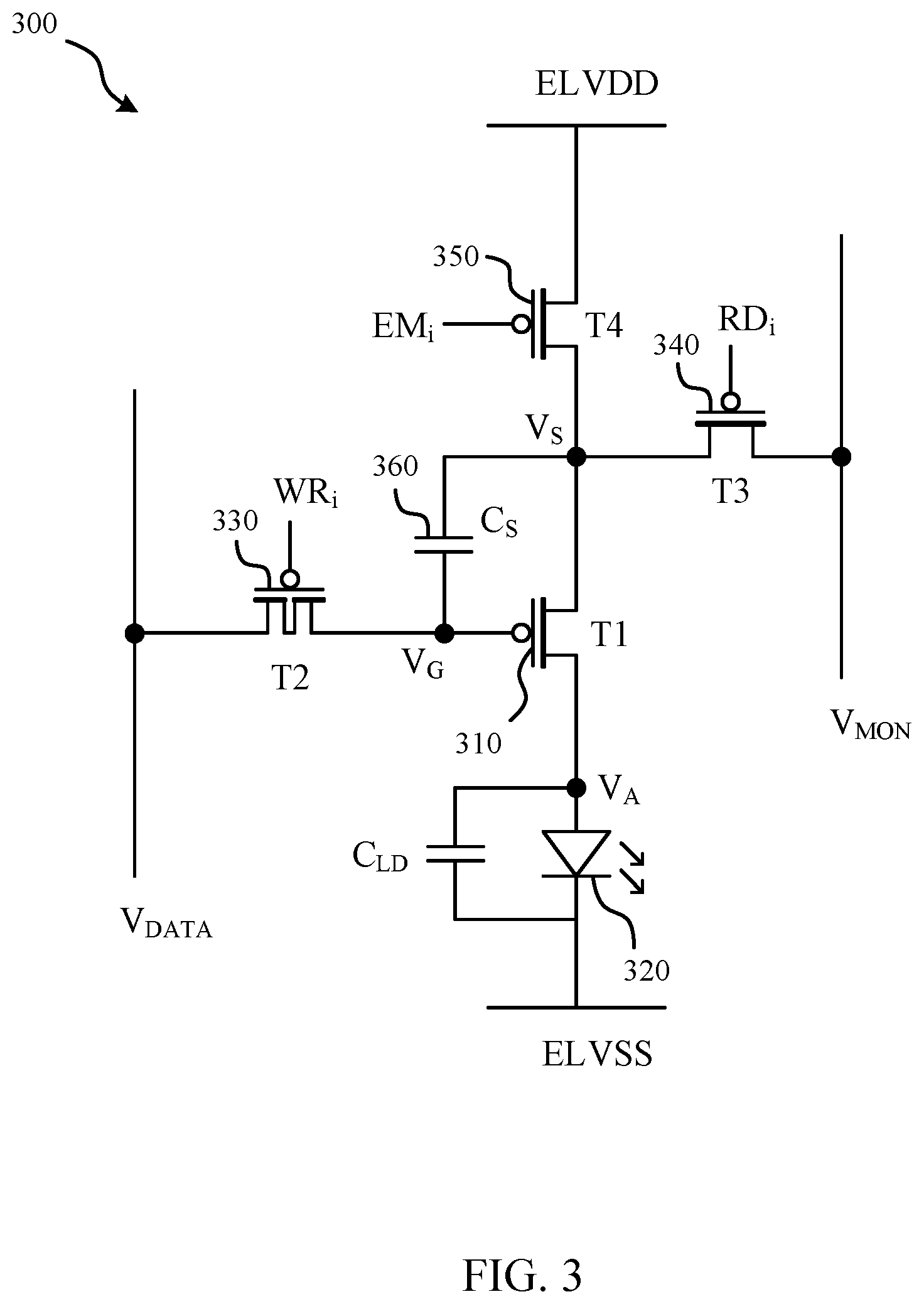
With reference to FIG. 3, the structure of a four transistor single capacitor (4T1C) pixel circuit 300 according to an embodiment utilizing in-pixel compensation will now be described. The 4T1C pixel circuit 300 corresponds, for example, to a single pixel 110 in the ith row of the display system 150 depicted in FIG. 1. The 4T1C pixel circuit 300 depicted in FIG. 3 is based on NMOS transistors. It should be understood that variations of this pixel and its functioning are contemplated and include different types of transistors (PMOS, NMOS, or CMOS) and different semiconductor materials (e.g. LTPS, Metal Oxide, etc.).
The 4T1C pixel circuit 300 includes a driving transistor 310 (T1), a light emitting device 320, a first switch transistor 330 (T2), a second switch transistor 340 (T3), a third switch transistor 350 (T4), and a storage capacitor 360 (Cs). Each of the driving transistor 310, the first switch transistor 330, the second switch transistor 340, and the third switch transistor 350 having first, second, and gate terminals, and each of the light emitting device 320 and the storage capacitor 360 having first and second terminals.
The gate terminal of the driving transistor 310 is coupled to a first terminal of the storage capacitor 360, while the first terminal of the driving transistor 310 is coupled to the second terminal of the storage capacitor 360, and the second terminal of the driving transistor 310 is coupled to the first terminal of the light emitting device 320. The gate terminal of the first switch transistor 330 is coupled to a write signal line (WR.sub.i) of the ith row, while the first terminal of the first switch transistor 330 is coupled to a data line (V.sub.DATA), and the second terminal of the first switch transistor 330 is coupled to the gate terminal of the driving transistor 310. A node common to the gate terminal of the driving transistor 310 and the storage capacitor 360 as well as the first switch transistor 330 is labelled by its voltage V.sub.G in the figure. The gate terminal of the second switch transistor 340 is coupled to a read line (RD.sub.i) of the ith row, while the first terminal of the second switch transistor 340 is coupled to a monitor line (V.sub.MON), and the second terminal of the second switch transistor 340 is coupled to the second terminal of the storage capacitor 360. The gate terminal of the third switch transistor 350 is coupled to an emission signal line (EM.sub.i) of the ith row, while the first terminal of the third switch transistor 350 is coupled to a first reference potential ELVDD, and the second terminal of the third switch transistor 350 is coupled to the second terminal of the storage capacitor 360. A node common to the second terminal of the storage capacitor 360, the driving transistor 310, the second switch transistor 340, and the third switch transistor 350 is labelled by its voltage V.sub.S in the figure. The second terminal of the light emitting device 320 is coupled to a second reference potential ELVSS. A capacitance of the light emitting device 320 is depicted in FIG. 3 as C.sub.LD. In some embodiments, the light emitting device 320 is an OLED.
The 4T1C pixel circuit 300 of FIG. 3, as will become apparent from the description of its functioning below, is capable of achieving a good level of in-pixel compensation which is useful for mitigating the hysteresis effects in the driving transistor 310.
With reference also to FIG. 4, an example of a display timing 400 for the 4T1C pixel circuit 300 depicted in FIG. 3 will now be described. The complete display timing 400 occurs typically once per frame and includes a programming cycle 410, a calibration cycle 420, a settling cycle 430, and an emission cycle 440. During the programming cycle 410 over a period T.sub.RD, the read signal (RD.sub.i) and write signal (WR.sub.i) are held low while the emission (EM.sub.i) signal is held high. The emission signal (EM.sub.i) is held high throughout the programming, calibration, and settling cycles 410 420 430 to ensure the third switch transistor 350 remains OFF during those cycles (T.sub.EM).
During the programming cycle 410 the first switch transistor 330 and the second switch transistor 340 are both ON. The voltage of the storage capacitor 360 and therefore the voltage V.sub.SG of the driving transistor 310 is charged to a value of V.sub.MON-V.sub.DATA where V.sub.MON is a voltage of the monitor line and V.sub.DATA is a voltage of the data line. These voltages are set in accordance with a desired programming voltage for causing the pixel 300 to emit light at a desired luminance according to image data.
At the beginning of the calibration cycle 420, the read signal (RD.sub.i) goes high to turn OFF the second switch transistor 340 to discharge some of the voltage (charge) of the storage capacitor 360 through the driving transistor 310. The amount discharged is a function of the characteristics of the driving transistor 310. For example, if the driving transistor 310 is "strong", the discharge occurs relatively quickly and relatively more charge is discharged from the storage capacitor 360 through the driving transistor 310 during the fixed duration of the calibration cycle 420. On the other hand, if the driving transistor 310 is "weak", the discharge occurs relatively slowly and relatively less charge is discharged from the storage capacitor 360 through the driving transistor 310 during the calibration cycle 420. As a result, the voltage (charge) stored in the storage capacitor 360 (V.sub.P) is reduced comparatively more for relatively strong driving transistors versus comparatively less for relatively weak driving transistors, thereby providing some compensation for non-uniformity and variations in the driving transistors across the display whether due to variations in fabrication, variations in degradation over time, or variations due to hysteresis in the temporary threshold voltage of the driving transistor 310.
After the calibration cycle 420, a settling cycle 430 is performed prior to the emission. During the settling cycle 430 the second and third switch transistors 340, 350 remain OFF, while the write signal (WR.sub.i) goes high to also turn OFF the first switch transistor 330. After completion of the duration of the settling cycle 430 at the start of the emission cycle 440, the emission signal (EM.sub.i) goes low turning ON the third switch transistor 350 allowing current to flow through the light emitting device 320 according to the calibrated stored voltage on the storage capacitor 360.
Although the pixel 300 circuit is capable of achieving in-pixel compensation including that related to hysteresis to a good level for high and medium grayscales, low grayscale compensation may be insufficient to meet high-end uniformity specifications.
With reference to FIG. 5, the structure of a five transistor, single capacitor (5T1C) pixel circuit 500 according to an embodiment will now be described. The 5T1C pixel circuit 500 corresponds, for example, to a single pixel 110 in the ith row of the display system 150 depicted in FIG. 1. The 5T1C pixel circuit 500 depicted in FIG. 5 is based on NMOS transistors. It should be understood that variations of this pixel and its functioning are contemplated and include different types of transistors (PMOS, NMOS, or CMOS) and different semiconductor materials (e.g. LTPS, Metal Oxide, etc.).
The 5T1C pixel circuit 500 includes a driving transistor 510 (T1), a light emitting device 520, a first switch transistor 530 (T2), a second switch transistor 540 (T3), a third switch transistor 550 (T4), and a storage capacitor 560 (Cs) in substantially the same configuration as that of the 4T1C pixel circuit 300 of FIG. 3. The 5T1C pixel circuit 500 also includes a reset switch transistor 570 (T5) coupled between ELVDD and a node between the first switch transistor 530 and the storage capacitor 560.
The gate terminal of the driving transistor 510 is coupled to a first terminal of the storage capacitor 560, while the first terminal of the driving transistor 510 is coupled to the second terminal of the storage capacitor 560, and the second terminal of the driving transistor 510 is coupled to the first terminal of the light emitting device 520. The gate terminal of the first switch transistor 530 is coupled to a write signal line (WR.sub.i) of the ith row, while the first terminal of the first switch transistor 530 is coupled to a data line (V.sub.DATA), and the second terminal of the first switch transistor 530 is coupled to the gate terminal of the driving transistor 510. A node common to the gate terminal of the driving transistor 510 and the storage capacitor 560 as well as the first switch transistor 530 is labelled by its voltage V.sub.G in the figure. The gate terminal of the second switch transistor 540 is coupled to a read line (RD.sub.i) of the ith row, while the first terminal of the second switch transistor 540 is coupled to a monitor line (V.sub.MON), and the second terminal of the second switch transistor 540 is coupled to the second terminal of the storage capacitor 560. The gate terminal of the third switch transistor 550 is coupled to an emission signal line (EM.sub.i) of the ith row, while the first terminal of the third switch transistor 550 is coupled to a first reference potential ELVDD, and the second terminal of the third switch transistor 550 is coupled to the second terminal of the storage capacitor 560. A node common to the second terminal of the storage capacitor 560, the driving transistor 510, the second switch transistor 540, and the third switch transistor 550 is labelled by its voltage V.sub.S in the figure. The second terminal of the light emitting device 520 is coupled to a second reference potential ELVSS. A capacitance of the light emitting device 520 is depicted in FIG. 5 as C.sub.LD. In some embodiments, the light emitting device 520 is an OLED.
As mentioned above, the 5T1C pixel circuit 500 includes a reset switch transistor 570 coupled between the gate terminal of the drive transistor 510 and the first reference potential ELVDD. The first terminal of the reset switch transistor 570 is coupled to the first reference potential ELVDD and the second terminal of the reset switch transistor 570 is coupled to the node V.sub.G common to the first switch transistor 530, the storage capacitor 560, and the driving transistor 510. The gate terminal of the reset switch transistor 570 is coupled to a read or write signal line of a different row, for example, the read line RD.sub.i-1 of the (i-1)th row or the write signal line WR.sub.i-1 of the (i-1)th row. The 5T1C pixel circuit 500 is capable of achieving both a good level of in-pixel compensation if so driven (which is useful for mitigating the hysteresis effects in the driving transistor 510) as well as being capable of releasing charges trapped in the channel of the driving transistor 510 through the reset cycle described further below.
With reference to FIG. 6, the structure of a modified implementation of a five transistor, single capacitor (5T1C) pixel circuit 600 according to an embodiment will now be described. The modified 5T1C pixel circuit 600 corresponds, for example, to a single pixel 110 in the ith row of the display system 150 depicted in FIG. 1. The modified 5T1C pixel circuit 600 depicted in FIG. 6 is based on NMOS transistors. It should be understood that variations of this pixel and its functioning are contemplated and include different types of transistors (PMOS, NMOS, or CMOS) and different semiconductor materials (e.g. LTPS, Metal Oxide, etc.).
The modified 5T1C pixel circuit 600 includes a driving transistor 610 (T1), a light emitting device 620, a first switch transistor 630 (T2), a second switch transistor 640 (T3), a third switch transistor 650 (T4), a storage capacitor 660 (Cs), and a reset switch transistor 670 (T5) in substantially the same configuration as that of the 5T1C pixel circuit 500 of FIG. 5. The modified 5T1C pixel circuit 600 differs from the pixel circuit 500 only in that the gate terminal of the second switch transistor 640 is coupled to the write signal line (WR.sub.i) of the ith row (to which the gate terminal of the first switch transistor 630 is also coupled), and the gate terminal of the reset switch transistor 670 is coupled to a write signal line of a different row, namely, the write signal line WR.sub.i-1 of the (i-1)th row. This simplifies row (gate) control signals required per row of pixels of the display system 150.
The modified 5T1C pixel circuit 600, in a similar manner as the 5T1C 500 pixel circuit is capable of releasing charges trapped in the channel of the driving transistor 510 through the reset cycle described below.
With reference also to FIG. 7, an example of a display timing 700 for 5T1C pixel circuits 500 and 600 of the ith row depicted in FIGS. 5-6 will now be described. The complete display timing 700 occurs typically once per frame and includes a post-emission settling cycle 702 (which occurs after a previous emission cycle 740x of a previous frame), a reset cycle 704, a first settling cycle 706, a programming cycle 710, first and second pre-emission settling cycles 730a, 730b, and an emission cycle 740.
At the end of the previous emission cycle 740x and the beginning of the post-emission settling cycle 702, the emission signal is (EM.sub.i) is switched from low to high in order to turn OFF the third switch transistor 550, 650. During non-emission cycles 702, 704, 706, 710, 730a, 730b the emission (EM.sub.i) signal is held high to ensure the third switch transistor 550 or 650 remains OFF during those cycles.
During the post-emission settling cycle 702 each of the transistors of the pixel circuit 500 600 is OFF allowing the voltage V.sub.S to settle to V.sub.OLED (the turn on voltage of the light emitting device 520 620), while the voltage V.sub.G to settle to the voltage of the light emitting device minus a voltage on the storage capacitor 560 660 related to a pixel programming of the pixel during the previous frame (V.sub.OLED-V.sub.P1).
After a duration of the post-emission settling cycle 702, a sufficient settling time for V.sub.S to settle to a low voltage, the write or read signal controlling the reset switch transistor 570 670, namely read signal RD.sub.i-1 for the (i-1)th row, or write signal WR.sub.i-1 for the (i-1)th row, switches from high to low, turning the reset switch transistor 570 670 ON, which charges node V.sub.G up to ELVDD during the reset cycle 704. Since V.sub.S has been discharged to a low voltage of V.sub.OLED which is much less than ELVDD, during reset cycle 704 V.sub.SG goes less than zero, the driving transistor 510 610 becomes negatively biased which triggers the release of carriers and hence reversal of the short-term trapping of carriers, resetting the driving transistor 510 610 and its threshold voltage (V.sub.TH), and mitigating hysteresis in the I-V response exhibited by the driving transistor 510 610 when it is programmed in the following programming cycle 710. The negative biasing utilizing the ELVDD rail is programming independent and provides a high magnitude of reverse biasing for effective release of carriers and hence reduction of hysteresis effects.
After the reset cycle 704, the read signal RD.sub.i-1 for the (i-1)th row, or write signal WR.sub.i-1 for the (i-1)th row, switches from low to high, turning the reset switch transistor 570 670 OFF. For a relatively short first settling cycle 706, each of the transistors of the pixel circuit 500 600 are OFF. Following the first settling cycle 706, during the programming cycle 710, both the first switch transistor 530 630 and the second switch transistor 540 640 are turned ON.
For embodiments which include distinct read RD and write WR control signals, such as for the 5T1C pixel circuit 500, the read signal RD.sub.i for the ith row, and the write signal WR.sub.i for the ith row both switch from high to low, turning both the first switch transistor 530 and the second switch transistor 540 ON. For embodiments with only a write signal WR such as for the 5T1C pixel circuit 600, the write signal WR.sub.i for the ith row switches from high to low, turning both the first switch transistor 630 and the second switch transistor 640 ON.
This exposes the f
D00000
D00001
D00002
D00003
D00004
D00005
D00006
D00007
D00008
D00009
D00010
XML
uspto.report is an independent third-party trademark research tool that is not affiliated, endorsed, or sponsored by the United States Patent and Trademark Office (USPTO) or any other governmental organization. The information provided by uspto.report is based on publicly available data at the time of writing and is intended for informational purposes only.
While we strive to provide accurate and up-to-date information, we do not guarantee the accuracy, completeness, reliability, or suitability of the information displayed on this site. The use of this site is at your own risk. Any reliance you place on such information is therefore strictly at your own risk.
All official trademark data, including owner information, should be verified by visiting the official USPTO website at www.uspto.gov. This site is not intended to replace professional legal advice and should not be used as a substitute for consulting with a legal professional who is knowledgeable about trademark law.