Two-step deposition process
Snaith , et al.
U.S. patent number 10,580,585 [Application Number 15/323,823] was granted by the patent office on 2020-03-03 for two-step deposition process. This patent grant is currently assigned to OXFORD UNIVERSITY INNOVATION LIMITED. The grantee listed for this patent is OXFORD UNIVERSITY INNOVATION LIMITED. Invention is credited to James M. Ball, Giles E. Eperon, Henry J. Snaith.


View All Diagrams
| United States Patent | 10,580,585 |
| Snaith , et al. | March 3, 2020 |
| **Please see images for: ( Certificate of Correction ) ** |
Two-step deposition process
Abstract
The present invention provides a process for producing a layer of a crystalline material comprising a perovskite or a hexahalometallate, which process comprises: (i) exposing a substrate to a vapour comprising a first precursor compound in a first chamber to produce a layer of the first precursor compound on the substrate; and (ii) exposing the layer of the first precursor compound to a vapour comprising a second precursor compound in a second chamber to produce the layer of a crystalline material, wherein the pressure in the second chamber is above high vacuum. The invention also provides a process for producing a layer of a crystalline material comprising a perovskite or a hexahalometallate, which process comprises exposing a layer of a first precursor compound on a substrate to a vapour comprising a second precursor compound in a chamber to produce the layer of a crystalline material, wherein the pressure in the chamber is greater than high vacuum and less than atmospheric pressure. The invention also provides a process for producing a semiconductor device comprising a layer of a crystalline material, which process comprises producing said layer of a crystalline material by a process as according to the invention.
| Inventors: | Snaith; Henry J. (Oxford, GB), Eperon; Giles E. (Oxford, GB), Ball; James M. (Oxford, GB) | ||||||||||
|---|---|---|---|---|---|---|---|---|---|---|---|
| Applicant: |
|
||||||||||
| Assignee: | OXFORD UNIVERSITY INNOVATION
LIMITED (Botley, Oxford, GB) |
||||||||||
| Family ID: | 51410859 | ||||||||||
| Appl. No.: | 15/323,823 | ||||||||||
| Filed: | July 9, 2015 | ||||||||||
| PCT Filed: | July 09, 2015 | ||||||||||
| PCT No.: | PCT/GB2015/051993 | ||||||||||
| 371(c)(1),(2),(4) Date: | January 04, 2017 | ||||||||||
| PCT Pub. No.: | WO2016/005758 | ||||||||||
| PCT Pub. Date: | January 14, 2016 |
Prior Publication Data
| Document Identifier | Publication Date | |
|---|---|---|
| US 20170148579 A1 | May 25, 2017 | |
Foreign Application Priority Data
| Jul 9, 2014 [GB] | 1412201.4 | |||
| Current U.S. Class: | 1/1 |
| Current CPC Class: | H01L 51/422 (20130101); H01L 51/0077 (20130101); H01L 51/0002 (20130101); C23C 16/45553 (20130101); C23C 16/45557 (20130101); H01G 9/2009 (20130101); H01L 51/0032 (20130101); C23C 14/12 (20130101); C23C 14/0694 (20130101); C23C 14/5846 (20130101); C23C 14/0021 (20130101); H01G 9/2027 (20130101); C23C 16/409 (20130101); H01L 51/006 (20130101); C23C 14/24 (20130101); C23C 14/5893 (20130101); H01L 51/4226 (20130101); H01L 2251/306 (20130101); Y02P 70/50 (20151101); H01L 51/0056 (20130101); Y02P 70/521 (20151101); Y02E 10/549 (20130101); H01L 2031/0344 (20130101); Y02E 10/542 (20130101) |
| Current International Class: | H01L 21/00 (20060101); C23C 14/06 (20060101); C23C 14/12 (20060101); C23C 14/58 (20060101); C23C 14/00 (20060101); C23C 16/455 (20060101); H01L 51/42 (20060101); H01G 9/20 (20060101); C23C 14/24 (20060101); C23C 16/40 (20060101); H01L 51/00 (20060101); H01L 31/0256 (20060101) |
References Cited [Referenced By]
U.S. Patent Documents
| 5618761 | April 1997 | Eguchi et al. |
| 6391803 | May 2002 | Kim et al. |
| 7858144 | December 2010 | Freeman et al. |
| 2004/0058492 | March 2004 | Tatsumi |
| 2005/0045092 | March 2005 | Wu et al. |
| 2011/0318888 | December 2011 | Komatsu et al. |
| 2012/0021570 | January 2012 | Tajima et al. |
| 2013/0171349 | July 2013 | Takahashi |
| 103682153 | Mar 2014 | CN | |||
| 2012003341 | Jan 2012 | WO | |||
| 2014045021 | Mar 2014 | WO | |||
Other References
|
Ball, et al., Low-Temperature Processed Meso-Superstructured to Thin-Film Perovskite Solar Cells, Energy & Environmental Science, 2013, 6:1739-1743. cited by applicant . Burschka, et al., Sequential Deposition as a Route to High-Performance Perovskite-Sensitized Solar Cells, Nature, 2013, 499:316-319. cited by applicant . Chen, et al., Planar Heterojunction Perovskite Solar Cells Via Vapor-Assisted Solution Process, Journal of the American Chemical Society, 2013, 136(2):622-625. cited by applicant . Eperon, et al., Formamidinium Lead Trihalide: A Broadly Tunable Perovskite for Efficient Planar Heterojunction Solar Cells, Energy & Environmental Science, 2014, 7:982-988. cited by applicant . Eperon, et al., Morphological Control for High Performance, Solution-Processed Planar Heterojunction Perovskite Solar Cells, Advanced Functional Materials, 2014, 24:151-157. cited by applicant . Ha, et al., Synthesis of Organic-Inorganic Lead Halide Perovskite Nanoplatelets: Towards High-Performance Perovskite Solar Cells and Optoelectronic Devices, Advanced Optical Materials, 2014, 2(9):838-844. cited by applicant . Haber, Manual on Catalyst Characterization, Pure & Appl. Chem., 1991, 63(9):1227-1246. cited by applicant . Hu, et al., Vapour-Based Processing of Hole-Conductor-Free CH3NH3PbI3 perovskite/C60 Fullerene Planar Solar Cells, RSC Advances, 2014, 4:28964-28967. cited by applicant . Kim, et al., Lead Iodide Perovskite Sensitized All-Solid-State Submicron Thin Film Mesoscopic Solar Cell With Efficiency Exceeding 9%, Scientific Reports, 2012, 2: 591, 7 pp. cited by applicant . Kitazawa, et al., Optical Properties of Organic-Inorganic Hybrid Films Prepared by the Two-Step Growth Process, Journal of Luminescence, 2009, 129:1036-1041. cited by applicant . Liu, D., et al., Perovskite Solar Cells with a Planar Heterojunction Structure Prepared Using Room-Temperature Solution Processing Techniques, Nature Photonics, 2014, 8:133-138. cited by applicant . Liu, M., et al., Efficient Planar Heterojunction Perovskite Solar Cells by Vapour Deposition, Nature, 2013, 501:395-398. cited by applicant . Noh, et al., Chemical Management for Colorful, Efficient and Stable Inorganic-Organic Hybrid Nanostructured Solar Cells, Nano Letters, 2013, 13(4):1764-1769. cited by applicant . Rouquerol, et al., Recommendations for the Characterization of Porous Solids, Pure & Appl. Chem., 1994, 66(8):1739-1758. cited by applicant . Sing, et al., Reporting Physisorption Data for Gas/Solid Systems With Special Reference to the Determination of Surface Area and Porosity, Pure & Appl. Chem., 1985, 57(4):603-619. cited by applicant . Stranks, et al., Electron-Hole Diffusion Lengths Exceeding 1 Micrometer in an Organometal Trihalide Perovskite Absorber, Science, 2013, 342:341-344. cited by applicant . Yoon, et al., Vapor Deposition of Organic-Inorganic Hybrid Perovskite Thin-Films for Photovoltaic Applications, In Photovoltaic Specialist Conference (PVSC), 2014 IEEE 40th, pp. 1577-1580. cited by applicant . George, Atomic Layer Deposition: An Overview, Chem. Rev., 2010, 110:111-131. cited by applicant . The State Intellectual Property Office of China, First Office Action, Application No. 201580037211.5, dated Jul. 17, 2018, 14 pages. cited by applicant. |
Primary Examiner: Booth; Richard A
Attorney, Agent or Firm: Quarles & Brady LLP
Claims
The invention claimed is:
1. A process for producing a layer of a crystalline material comprising a perovskite or a hexahalometallate, which process comprises: (i) a physical vapour deposition step comprising exposing a substrate to a vapour comprising a first precursor compound in a first chamber to produce a layer of the first precursor compound on the substrate; and (ii) a chemical vapour deposition step comprising exposing the layer of the first precursor compound to a vapour comprising a second precursor compound in a second chamber to produce the layer of a crystalline material, wherein: the pressure in the first chamber is less than or equal to 10.sup.-3 mbar; the pressure in the second chamber is greater than or equal to 1 mbar; the first precursor compound comprises one or more first cations and one or more first anions; and the second precursor compound comprises one or more organic cations and one or more second anions.
2. A process according to claim 1, wherein in step (i) the substrate is exposed to a directional vapour comprising the first precursor compound.
3. A process according to claim 1, wherein in step (ii) the layer of the first precursor compound is exposed to a non-directional vapour comprising the second precursor compound.
4. A process according to claim 1, wherein the crystalline material consists essentially of a perovskite or a hexahalometallate.
5. A process according to claim 1, wherein the crystalline material comprises a perovskite of formula (II): [A][B][X].sub.3 (II) wherein: [A] is at least one organic monocation; [B] is at least one metal cation, wherein [B] comprises at least one selected from Ca.sup.2+, Sr.sup.2+, Cd.sup.2+,Cu.sup.2+, Ni.sup.2+, Mn.sup.2+, Fe.sup.2+, Co.sup.2+, Pd.sup.2+, Ge.sup.2+, Sn.sup.2+, Pb.sup.2+, Yb.sup.2+ and Eu.sup.2+; and [X] is at least one halide anion.
6. A process according to claim 5, wherein [A] comprises one or more organic cations selected from (CH.sub.3NH.sub.3).sup.+, (CH.sub.3CH.sub.2NH.sub.3).sup.+, (CH.sub.3CH.sub.2CH.sub.2NH.sub.3).sup.+, (N(CH.sub.3).sub.4).sup.+, (H.sub.2N--C(H).dbd.NH.sub.2).sup.+ and (H.sub.2N--C(CH.sub.3).dbd.NH.sub.2).sup.+.
7. A process according to claim 5, wherein [A] comprises one or more cations selected from (CH.sub.3NH.sub.3).sup.+, (H.sub.2N--C(H).dbd.NH.sub.2).sup.+ and Cs.sup.+.
8. A process according to claim 1, wherein the crystalline material comprises a hexahalometallate of formula (III): [A].sub.2[B][X].sub.6 (III) wherein: [A] is at least one organic monocation; [M] is at least one metal or metalloid tetracation; and [X] is at least one halide anion.
9. A process according to claim 1, wherein the pressure in the first chamber is less than or equal to 10.sup.-3 mbar.
10. A process according to claim 1, wherein the first chamber and the second chamber are the same chamber or different chambers.
11. A process according to claim 1, wherein the mean free path of the vapour of the first precursor compound is greater than or equal to 10 mm or the mean free path of the vapour of the second precursor compound is less than or equal to 0.1 mm.
12. A process according to claim 1, wherein the temperature of the second chamber is greater than or equal to 100.degree. C.
13. A process according to claim 1, wherein (i) the first precursor compound comprises a metal cation and one or more first anions and (ii) the second precursor compound comprises an organic monocation and one or more second anions.
14. A process according claim 13, wherein the metal cation is selected from Ca.sup.2+, Sr.sup.2+, Cd.sup.2+, Cu.sup.2+, Ni.sup.2+, Mn.sup.2+, Fe.sup.2+, Co.sup.2+, Pd.sup.2+, Ge.sup.2+, Sn.sup.2+, Pb.sup.2+, Yb.sup.2+, Eu.sup.2+, Pd.sup.4+, W.sup.4+, Re.sup.4+, Os.sup.4+, Ir.sup.4+, Pt.sup.4+, Sn.sup.4+, Pb.sup.4+, Ge.sup.4+, and Te.sup.4+; the one or more first anions are selected from halide anions; the organic monocation is selected from an organic ammonium cation and an organic formamidinium cation, or a caesium cation; and the one or more second anions is a halide anion.
15. A process according to claim 14, wherein: the metal cation is selected from Cu.sup.2+, Ge.sup.2+, Sn.sup.2+, Pb.sup.2+; the one or more first anions are selected from F.sup.-, Cl.sup.-, Br.sup.-, and I.sup.-; the monocation is selected from organic cations of formula (R.sup.5NH.sub.3).sup.+wherein R.sup.5 is a unsubstituted or substituted C.sub.1-20 alkyl group or an unsubstituted or substituted aryl group; or the one or more second anions are selected from F.sup.-, Cl.sup.-, Br.sup.-, and I.sup.-.
16. A process according to claim 13, wherein: the first precursor compound is a compound of formula BX.sub.2 wherein B is said metal cation and X is a halide anion; or the second precursor compound is a compound of formula AX' wherein A is said organic monocation and X' is a halide anion.
17. A process according to claim 1, wherein the first precursor compound is a lead dihalide, a tin dihalide or a copper dihalide, and the second precursor compound is an alkylammonium halide, a formamidinium halide or a caesium halide.
18. A process according to claim 1, wherein the substrate comprises a layer of an n-type semiconductor or a layer of a p-type semiconductor.
19. A process according to claim 1, wherein the substrate comprises a layer of a porous scaffold material.
20. A process according to claim 1, wherein the thickness of the layer of the first precursor compound is from 50 nm to 1000 nm.
21. A process according to claim 1, which process further comprises: (iii) exposing the layer of the crystalline material to a vapour comprising a solvent.
22. A process according to claim 1, which process further comprises: (iv) heating the layer of the crystalline material to a temperature of from 50.degree. C. to 250.degree. C.
23. A process for producing a semiconductor device comprising a layer of a crystalline material, wherein the process comprises producing said layer of a crystalline material by a process comprising: (i) a physical vapour deposition step comprising exposing a substrate to a vapour comprising a first precursor compound in a first chamber to produce a layer of the first precursor compound on the substrate; and (ii) a chemical vapour deposition step comprising exposing the layer of the first precursor compound to a vapour comprising a second precursor compound in a second chamber to produce the layer of a crystalline material, wherein: the pressure in the first chamber is less than or equal to 10.sup.-3 mbar; the pressure in the second chamber is greater than or equal to 1 mbar; the first precursor compound comprises one or more first cations and one or more first anions; and the second precursor compound comprises one or more organic cations and one or more second anions.
24. A process according to claim 23, which process further comprises disposing on the layer of a crystalline material a layer of a p-type semiconductor or a layer of a n-type semiconductor.
25. A process according to claim 24, which process further comprises disposing on the layer of the p-type semiconductor or n-type semiconductor a layer of a second electrode material.
26. A process according to claim 23, wherein the semiconductor device is an optoelectronic device.
27. A process according to claim 1, wherein the pressure in the second chamber is greater than or equal to 100 mbar.
Description
CROSS-REFERENCE TO RELATED APPLICATIONS
This application represents the national stage entry of PCT International Application No. PCT/GB2015/051993 filed Jul. 9, 2015 and claims priority to Great Britain Patent Application No. 1412201.4 filed on Jul. 9, 2014. The contents of this application are hereby incorporated by reference as if set forth in their entirety herein.
FIELD OF THE INVENTION
The present invention relates to a process for producing a layer of a crystalline material. A process for producing a semiconductor device comprising a layer of a crystalline material is also described.
The work leading to this invention has received funding from the European Community's Seventh Framework Programme (FP7/2007-2013) under grant agreement no. 279881.
BACKGROUND OF THE INVENTION
Hybrid organic-inorganic perovskite materials have recently become a topic of extreme interest for photovoltaics, with devices based on these materials now reaching power conversion efficiencies of above 15%. Other photoactive crystalline materials are also of substantial current interest.
The key to achieving the highest efficiencies with this material appears to be optimisation of the perovskite or crystalline material film quality. Typically, perovskite and other crystalline films have been deposited by spin-coating a precursor containing necessary components to form the perovskite: a metal halide and an organic component. However, spin-coating is by its very nature a process which can easily result in non-uniform films or films with pinholes. Spin-coating is highly susceptible to microscopic amounts of dust on the substrate, precipitates in the solution, local atmosphere composition and temperature, and human error when depositing. These factors combine to make spin-coating an inherently poorly reproducible process for producing organometal perovskites and other crystalline materials. Moreover, spin-coating is a process which cannot be easily scaled up.
A key breakthrough was achieved by Liu, Snaith et al. (Liu, M.; Johnston, M. B.; Snaith, H. J. Efficient Planar Heterojunction Perovskite Solar Cells by Vapour Deposition. Nature 2013, 501, 395-398), who describe a high vacuum two-source vapour deposition technique to produce extremely uniform, high quality perovskite films, resulting in the most efficient devices at the time. However, this is a costly process; it requires large quantities of the reagents as well as high temperatures and most importantly, a high vacuum chamber.
Additionally, due to the volatile nature of the organic component employed, it is difficult to control the rate of its deposition, making this process difficult to reproduce between batches.
A second breakthrough was achieved by Burschka et al. (Burschka, J.; Pellet, N.; Moon, S.-J.; Humphry-Baker, R.; Gao, P.; Nazeeruddin, M. K.; Grazel, M. Sequential Deposition as a Route to High-Performance Perovskite-Sensitized Solar Cells. Nature 2013, 499, 316-319) who describe a two-step deposition route to form high-quality perovskite films using solution-processing. The metal halide component is spin-coated on a meso-structured substrate and the layer of the metal halide is subsequently dipped in a solution containing the dissolved organic component. The perovskite film forms spontaneously. Recent research has pointed to planar perovskite heterojunction solar cells having the greatest potential to reach the highest efficiencies, rather than those based on a meso-structured (e.g. mesoporous) oxide, and hence the two-step approach was recently adapted for planar solar cells by Liu, Kelly et al. (Liu, D.; Kelly, T. L. Perovskite Solar Cells with a Planar Heterojunction Structure Prepared Using Room-Temperature Solution Processing Techniques. Nat. Photonics 2013, 1-6). This produced some of the most efficient perovskite solar cells to date. However, the films produced in this way are substantially non-uniform and the surface of the perovskite layer comprises large crystallites of greater than a micron in size. The presence of these crystallites causes high surface roughness. This is likely to be an issue in Willis of reproducibility: if an electrode touches a crystallite of the perovskite penetrating the hole-transport layer it can provide a recombination pathway, lowering device performance and affecting reproducibility. For the best solar cells, an extremely flat perovskite surface would be optimal, allowing only a thin layer of hole transporting material to be employed, and hence minimising resistive losses in that layer.
In light of this, the most recent development for making smooth perovskite films was made by Chen, Yang et al. (Chen, Q.; Zhou, H.; Hong, Z.; Luo, S.; Duan, H.-S.; Wang, H.-H.; Liu, Y.; Li, G.; Yang, Y. Planar Heterojunction Perovskite Solar Cells via Vapor Assisted Solution Process. J. Am. Chem. Soc. 2013, 3-6), who have modified the two-step deposition process, in the planar perovskite solar cell configuration, by replacing the solution-phase organic dipping step with an atmospheric pressure vapour-phase conversion, where the spincoated metal halide is annealed in an atmosphere of the sublimed organic component to convert it to the perovskite. This results in perovskite films of low roughness and high purity. However, this procedure still makes use of spin-coating to form the metal halide initial film, which results in the aforementioned issues with reproducibility and non-uniformity.
Kitazawa et al. (Kitazawa, N.; Yaemponga, D.; Aono, M.; Watanabe, Y. Optical Properties of Organicinorganic Hybrid Films Prepared by the Two-Step Growth Process. J. Lumin. 2009, 129, 1036-1041) describes a process to fabricate nanocrystal-sized (C.sub.8H.sub.17NH.sub.3)PbBr.sub.4, using two high vacuum stages. A first vacuum evaporation of a metal halide layer followed by a second vacuum evaporation of an organic halide. A sequential two-step vacuum deposition process is also described in Hu et al. (H. Hu, D. Wang, Y. Zhou, J. Zhang, S. Lv, S. Pang, X. Chen, Z. Liu, N. P. Padture and G. Cui, RSC Adv., 2014, DOI: 10.1039/C4RA03820G).
Methods which make use of vacuum evaporation to form the metal halide layer followed by completion of the perovskite by dipping the vacuum evaporated metal halide layer in a solution of the organic component have not succeeded in producing high quality films. The use of a second solution-based step results in unsuitable perovskite films comprising large crystals and unstable device performance (see Comparative Example 2).
Thus, it is an object of the invention to provide an effective process for the production of perovskite layers. In particular, it is desirable to produce layers of a crystalline material (e.g. perovskite) by a process which is readily reproducible, easy to scale up and produces layers of a crystalline material having a flat surface.
SUMMARY OF THE INVENTION
Here a new approach to prepare extremely smooth, pinhole-free perovskite (and other crystalline material) films of high purity, for use in photovoltaics and other optical and semiconducting applications is presented. The technique makes use of a two-stage vapour phase technique to ensure extremely high quality of films, with no solution-processing required at all. For instance, initially the metal halide can be deposited via thermal vapour deposition, under high vacuum, to produce a high quality, smooth and pinhole-free film. Subsequently, the film is placed and optionally heated in an atmosphere saturated with the sublimed organic component, causing it to undergo conversion to the perovskite. The advantage of this technique over the previously developed methods is two-fold. Firstly, no solution-processing is required, which enables the most uniform and high quality films to be produced. Secondly, by carrying out the film fabrication in two stages, and depositing the organic at relatively high pressures and relatively low temperatures, it is a much more controlled and reproducible method than the dual source, high vacuum method of Liu, Snaith et al. The process of the invention allows high efficiency perovskite solar cells to be fabricated, and furthermore can enable the fabrication of new perovskite or perovskite-like hybrid materials. The process of the invention circumvents the problems of prior art approaches (for instance Chen et al.) by employing solvent-free vapour deposition approaches. Furthermore, the use of a two-stage vapour process allows materials which have poor solubilities to be used. For instance, the process allows the production of new copper based materials.
The invention provides a process for producing a layer of a crystalline material that comprises a perovskite or a hexahalometallate, which process comprises: (i) exposing a substrate to a vapour comprising a first precursor compound in a first chamber to produce a layer of the first precursor compound on the substrate; and (ii) exposing the layer of the first precursor compound to a vapour comprising a second precursor compound in a second chamber to produce the layer of a crystalline material, wherein the pressure in the second chamber is greater than or equal to 1 mbar.
In step (i) the substrate may be exposed to a directional vapour comprising the first precursor compound. In step (ii) the layer of the first precursor compound may be exposed to a non-directional vapour comprising the second precursor compound. The first chamber and the second chamber are preferably different chambers.
The invention also provides a process for producing a layer of a crystalline material that comprises a perovskite or a hexahalometallate, which process comprises: (i) exposing a substrate to a vapour comprising a first precursor compound in a first chamber to produce a layer of the first precursor compound on the substrate, wherein the first chamber is under a high vacuum; and (ii) exposing the layer of the first precursor compound to a vapour comprising a second precursor compound in a second chamber to produce the layer of a crystalline material, wherein the second chamber is not under a high vacuum. Preferably, the pressure in the second chamber is also less than atmospheric pressure.
In step (i) the substrate may be exposed to a directional vapour comprising the first precursor compound. In step (ii) the layer of the first precursor compound may be exposed to a non-directional vapour comprising the second precursor compound. The first chamber and the second chamber are preferably different chambers.
The pressure in the first chamber may be less than or equal to 10.sup.-4 mbar, and preferably the pressure in the first chamber is less than or equal to 10.sup.-5 mbar. The pressure in the second chamber may be not less than 10.sup.-4 mbar, and preferably the pressure in the second chamber is greater than or equal to 1 mbar.
The invention also provides a layer of a crystalline material obtainable by a process according to the invention for producing a layer of a crystalline material.
The invention also provides a process for producing a semiconductor device comprising a layer of a crystalline material, which process comprises producing said layer of a crystalline material by a process according to the invention for producing a layer of a crystalline material. A semiconductor device obtainable by a process according to the invention is also provided.
BRIEF DESCRIPTION OF THE FIGURES
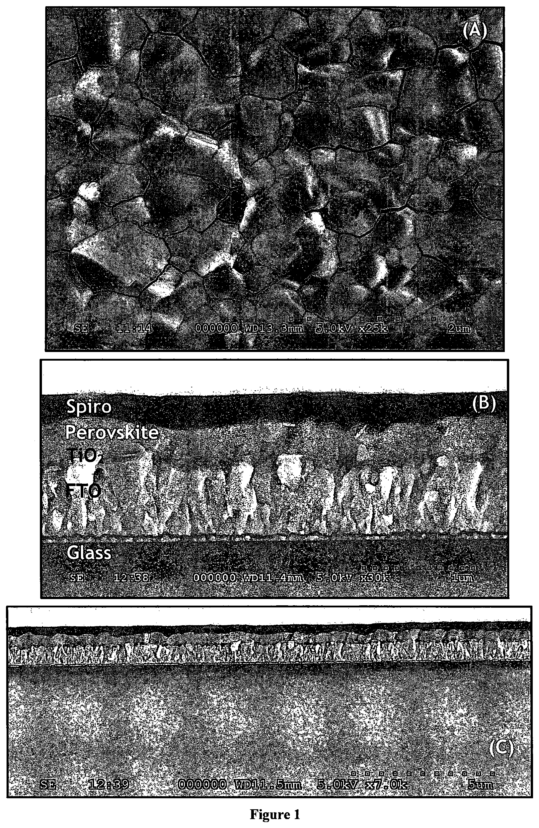
FIG. 1 shows scanning electron microscope images of (A) a top-view of a perovskite film grown by two-step vapour deposition, (B) short and (C) large scale cross-sections of devices incorporating a perovskite film grown by two-step vapour deposition.
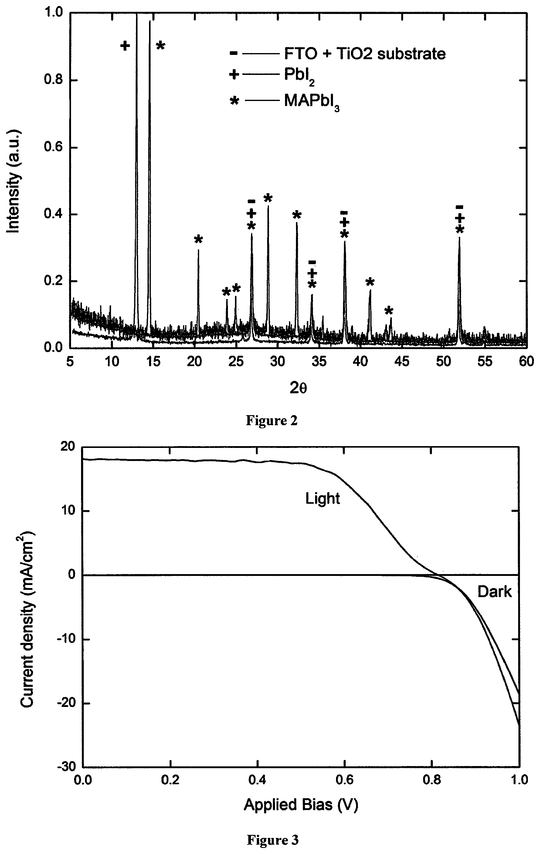
FIG. 2 shows an XRD pattern comparing evaporated PbI.sub.2 before (peaks marked with .sup.+) and after (peaks marked with *) MAI (methyl ammonium iodide) vapour treatment. This shows that after treatment all of the PbI.sub.2 is converted into MAPbI.sub.3. Additional peaks (marked with -) originating from the substrate are highlighted in the control spectrum.
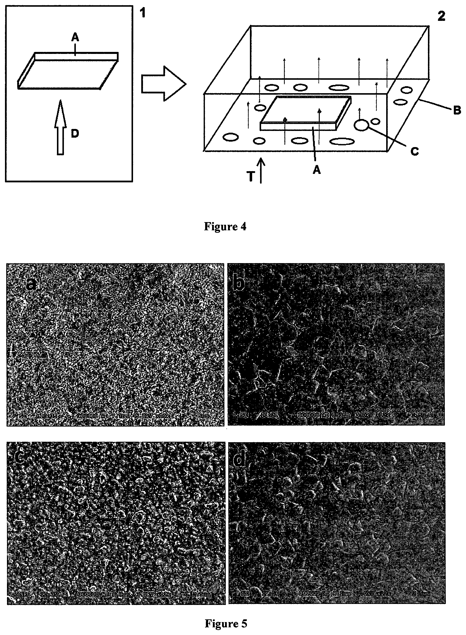
FIG. 3 shows current voltages characteristics under simulated AM1.5 sunlight (upper curve is light; lower curve is dark) for a device comprising a photoactive layer of methylammonium lead triiodide produced by a two-step vapour/vapour deposition.
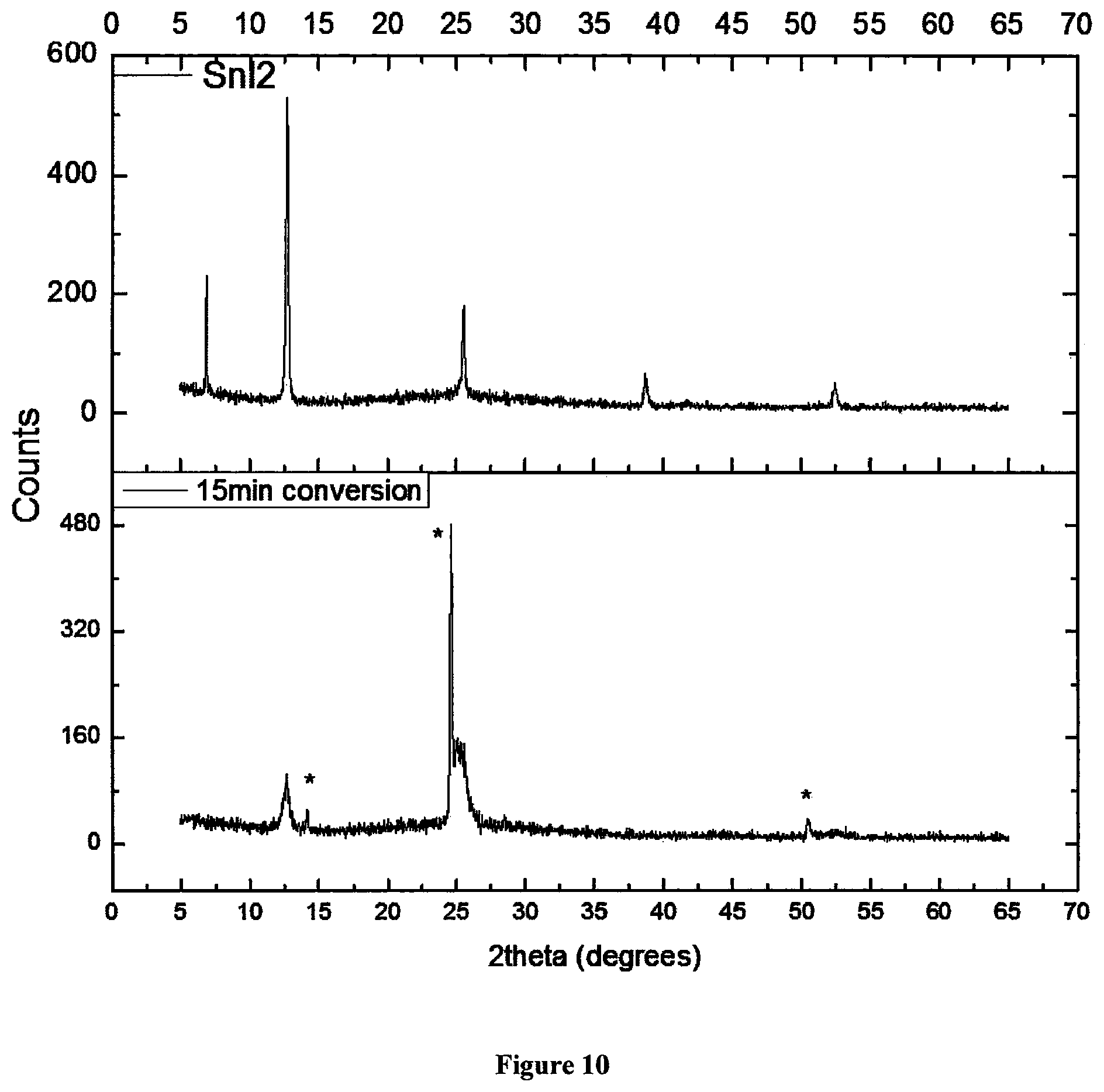
FIG. 4 shows a schematic diagram of an example of a two-step process according to the invention. In step 1 a substrate (A) is exposed to a vapour of a first precursor compound (for instance by vacuum deposition). In step 2 a substrate (A) comprising a layer of the first precursor compound is placed in a second chamber (B) together with solid second precursor compound (C) and the second chamber is heated (T) to produce a sublimed vapour of the second precursor compound.
FIG. 5 shows conversion of lead iodide to methylammonium lead triiodide via a two-stage process, one with spin-coated lead iodide and one with evaporated lead iodide. The Figure shows scanning electron micrographs of a) spin-coated lead iodide surface, b) methylammonium lead triiodide surface produced by atmospheric vapour phase organic treatment of spin-coated lead iodide, c) evaporated lead iodide surface, d) methylammonium lead triiodide surface produced by atmospheric vapour phase organic treatment of spin-coated lead iodide.
FIG. 6 shows X-ray diffraction patterns of a film of spin-coated lead iodide undergoing conversion to methylammonium lead triiodide after a certain time in the methylammonium iodide atmosphere. Total conversion is observed after .about.1 h 30 m. Horizontal axes represent 2.theta.. Vertical axes represent arbitrary units.
FIG. 7 shows UV-vis absorbance spectra of the methylammonium lead triiodide films produced from spin-coated lead iodide after a certain time in a methylammonium iodide atmosphere (30, 60 or 90 minutes).
FIG. 8 shows photovoltaic devices comprising methylammonium lead triiodide fabricated via organic vapour conversion of spin-coated and evaporated lead triiodide: a) cross-sectional SEM of device formed from converted spin-coated lead iodide; and b) cross-sectional SEM of device formed from converted evaporated lead iodide.
FIG. 9 shows current-voltage characteristics of methylammonium lead triiodide solar cells fabricated via spin-coated PbI.sub.2/vapour deposited MAI: as a planar heterojunction (upper); and on mesoporous TiO.sub.2 (lower).
FIG. 10 shows XRD spectra showing partial conversion of a film of spin-coated tin iodide into methylammonium tin triiodide, after treatment in a methylammonium iodide atmosphere. Perovskite peaks are labelled with a *.
FIG. 11 shows the XRD of a new copper-based material formed using a spin-coating metal halide/vapour deposited organic method with CuBr.sub.2 and methylammonium chloride.
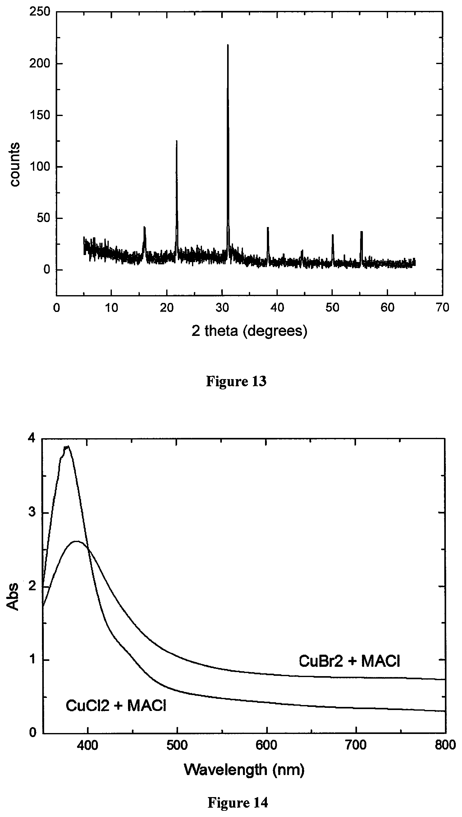
FIG. 12 shows the XRD of a copper-based material formed using a spin-coating metal halide/vapour deposited organic method with CuCl.sub.2 and methylammonium chloride.
FIG. 13 shows the XRD of a copper-based material formed using a spin-coating metal halide/vapour deposited organic method with CuCl.sub.2 and ammonium chloride.
FIG. 14 shows UV-Vis absorption of copper-based materials formed from CuBr.sub.2 and methylammonium chloride and CuCl.sub.2 and methylammonium chloride using a spin-coating metal halide/vapour deposited organic method.
FIG. 15 shows SEM images showing the evolution of perovskite crystal growth at room temperature by dip coating a PbCl.sub.2 thin-film into a 20 mg/ml isopropanol solution of methylammonium iodide after (a) 0 s, (b) 1 s, (c) 10 s, (d) 100 s, (e) 1000 s, (f) 10000 s.
FIG. 16 shows normalised XRD spectra for perovskite films at different dipping times, t.
FIG. 17 shows SEM images showing the evolution of perovskite crystal growth at room temperature by dip coating a PbI.sub.2 thin-film into a 20 mg/ml isopropanol solution of methylammonium iodide after (a) 0 s, (b) 1 s, (c) 10 s, (d) 100 s, (e) 1000 s, (f) 8000 s.
FIG. 18 shows normalised XRD spectra for perovskite films at different dipping times, t.
FIG. 19 shows morphology variation when forming perovskite from PbCl.sub.2 at 90.degree. C. after 500 seconds using the following MAI concentrations: (a) 3 mg/ml, (b) 4 mg/ml, (c) 5 mg/ml, (d) 6 mg/ml, (e) 7 mg/ml.
FIG. 20 shows morphology variation when forming perovskite from PbI.sub.2 at 90.degree. C. after 500 seconds using the following MAI concentrations: (a) 3 mg/ml, (b) 4 mg/ml, (c) 5 mg/ml, (d) 6 mg/ml, (e) 7 mg/ml.
FIG. 21 shows current density-voltage characteristics for the highest efficiency device based on an active layer formed by dip coating of a PbCl.sub.2 film at 90.degree. C. in a solution of 6.5 mg/ml MAI in isopropanol for 400s.
FIG. 22 shows a histogram of device efficiencies from 12 devices fabricated by vapour-solution method.
FIG. 23 shows a histogram of J-V curve stabilities for 12 devices fabricated by vapour-solution method.
FIG. 24 shows a top-view SEM of the surface of a formamidinium lead triiodide layer produced by two-step vapour deposition.
FIG. 25 shows a XRD pattern taken of a formamidinium lead triiodide layer produced by two-step vapour deposition.
FIG. 26 shows the UV-vis absorbance spectra of a formamidinium lead triiodide layer produced by two-step vapour deposition.
DETAILED DESCRIPTION OF THE INVENTION
Definitions
The term "perovskite", as used herein, refers to a material with a three-dimensional crystal structure related to that of CaTiO.sub.3 or a material comprising a layer of material, which layer has a structure related to that of CaTiO.sub.3. The structure of CaTiO.sub.3 can be represented by the formula ABX.sub.3, wherein A and B are cations of different sizes and X is an anion. In the unit cell, the A cations are at (0,0,0), the B cations are at (1/2, 1/2, 1/2) and the X anions are at (1/2, 1/2, 0). The A cation is usually larger than the B cation. The skilled person will appreciate that when A, B and X are varied, the different ion sizes may cause the structure of the perovskite material to distort away from the structure adopted by CaTiO.sub.3 to a lower-symmetry distorted structure. The symmetry will also be lower if the material comprises a layer that has a structure related to that of CaTiO.sub.3. Materials comprising a layer of perovskite material are well known. For instance, the structure of materials adopting the K.sub.2NiF.sub.4-type structure comprises a layer of perovskite material. The skilled person will appreciate that a perovskite material can be represented by the formula [A][B][X].sub.3, wherein [A] is at least one cation, [B] is at least one cation and [X] is at least one anion. When the perovskite comprises more than one A cation, the different A cations may distributed over the A sites in an ordered or disordered way. When the perovskite comprises more than one B cation, the different B cations may distributed over the B sites in an ordered or disordered way. When the perovskite comprise more than one X anion, the different X anions may distributed over the X sites in an ordered or disordered way. The symmetry of a perovskite comprising more than one A cation, more than one B cation or more than one X cation, will be lower than that of CaTiO.sub.3.
The term "metal halide perovskite", as used herein, refers to a perovskite, the formula of which contains at least one metal cation and at least one halide anion. The taint "organometal halide perovskite", as used herein, refers to a metal halide perovskite, the formula of which contains at least one organic cation.
The term "hexahalometallate", as used herein, refers to a compound which comprises an anion of the formula [MX.sub.6].sup.n- wherein M is a metal atom, each X is independently a halide anion and n is an integer from 1 to 4.
The term "chalcogenide" refers to anions of the elements of group 16, for instance O.sup.2-, S.sup.2-, Se.sup.2-, or Te.sup.2-. Typically, the chalcogenides are taken to be S.sup.2-, Se.sup.2-, and Te.sup.2-.
The term "monocation", as used herein, refers to any cation with a single positive charge, i.e. a cation of formula A.sup.+ where A is any moiety, for instance a metal atom or an organic moiety. The term "dication", as used herein, refers to any cation with a double positive charge, i.e. a cation of formula A.sup.2+ where A is any moiety, for instance a metal atom or an organic moiety. The term "tetracation", as used herein, refers to any cation with a quadruple positive charge, i.e. a cation of formula A.sup.4+ where A is any moiety, for instance a metal atom.
The term "alkyl", as used herein, refers to a linear or branched chain saturated hydrocarbon radical. An alkyl group may be a C.sub.1-20 alkyl group, a C.sub.1-14 alkyl group, a C.sub.1-10 alkyl group, a C.sub.1-6 alkyl group or a C.sub.1-4 alkyl group. Examples of a C.sub.1-10 alkyl group are methyl, ethyl, propyl, butyl, pentyl, hexyl, heptyl, octyl, nonyl or decyl. Examples of C.sub.1-6 alkyl groups are methyl, ethyl, propyl, butyl, pentyl or hexyl. Examples of C.sub.1-4 alkyl groups are methyl, ethyl, i-propyl, n-propyl, t-butyl, s-butyl or n-butyl. If the term "alkyl" is used without a prefix specifying the number of carbons anywhere herein, it has from 1 to 6 carbons (and this also applies to any other organic group referred to herein).
The term "cycloalkyl", as used herein, refers to a saturated or partially unsaturated cyclic hydrocarbon radical. A cycloalkyl group may be a C.sub.3-10 cycloalkyl group, a C.sub.3-8 cycloalkyl group or a C.sub.3-6 cycloalkyl group. Examples of a C3-8 cycloalkyl group include cyclopropyl, cyclobutyl, cyclopentyl, cyclohexyl, cyclohexenyl, cyclohex-1,3-dienyl, cycloheptyl and cyclooctyl. Examples of a C.sub.3-6 cycloalkyl group include cyclopropyl, cyclobutyl, cyclopentyl, and cyclohexyl.
The term "alkenyl", as used herein, refers to a linear or branched chain hydrocarbon radical comprising one or more double bonds. An alkenyl group may be a C.sub.2-20 alkenyl group, a C.sub.2-14 alkane group, a C.sub.2-10 alkenyl group, a C.sub.2-6 alkenyl group or a C.sub.2-4 alkenyl group. Examples of a C.sub.2-10 alkenyl group are ethenyl (vinyl), propenyl, butenyl, pentenyl, hexenyl, heptenyl, octenyl, nonenyl or decenyl. Examples of C.sub.2-6 alkenyl groups are ethenyl, propenyl, butenyl, pentenyl or hexenyl. Examples of C.sub.24 alkenyl groups are ethenyl, propenyl, n-propenyl, s-butenyl or n-butenyl. Alkenyl groups typically comprise one or two double bonds.
The term "alkynyl", as used herein, refers to a linear or branched chain hydrocarbon radical comprising one or more triple bonds. An alkynyl group may be a C.sub.2-20 alkynyl group, a C.sub.2-14 alkynyl group, a C.sub.2-10 alkynyl group, a C.sub.2-6 alkynyl group or a C.sub.2-4 alkynyl group. Examples of a C.sub.2-10 alkynyl group are ethynyl, propynyl, butynyl, pentynyl, hexynyl, heptynyl, octynyl, nonynyl or decynyl. Examples of C1-6 alkynyl groups are ethynyl, propynyl, butynyl, pentynyl or hexynyl. Alkynyl groups typically comprise one or two triple bonds.
The term "aryl", as used herein, refers to a monocyclic, bicyclic or polycyclic aromatic ring which contains from 6 to 14 carbon atoms, typically from 6 to 10 carbon atoms, in the ring portion. Examples include phenyl, naphthyl, indenyl, indanyl, anthrecenyl and pyrenyl groups. The term "aryl group", as used herein, includes heteroaryl groups. The term "heteroaryl", as used herein, refers to monocyclic or bicyclic heteroaromatic rings which typically contains from six to ten atoms in the ring portion including one or more heteroatoms. A heteroaryl group is generally a 5- or 6-membered ring, containing at least one heteroatom selected from O, S, N, P, Se and Si. It may contain, for example, one, two or three heteroatoms. Examples of heteroaryl groups include pyridyl, pyrazinyl, pyrimidinyl, pyridazinyl, fiiranyl, thienyl, pyrazolidinyl, pyrrolyl, oxazolyl, oxadiazolyl, isoxazolyl, thiadiazolyl, thiazolyl, isothiazolyl, imidazolyl, pyrazolyl, quinolyl and isoquinolyl.
The terms "alkylene", "cycloalkylene", "alkenylene", "alkynylene", and "arylene", as used herein, refer to bivalent groups obtained by removing a hydrogen atom from an alkyl, cycloalkyl, alkenyl, alkynyl, or aryl group, respectively. An alkylene group may be a C.sub.1-18 alkylene group, a C.sub.1-14 alkylene group, a C.sub.1-10 alkylene group, a C.sub.1-6 alkylene group or a C.sub.1-4 alkylene group. Examples of C.sub.1-6 alkylene groups are methylene, ethylene, propylene, butylene, pentylene and hexylene. A cycloalkylene group may be a C.sub.3-10 cycloalkylene group, a C.sub.3-8 cycloalkylene group or a C.sub.3-6 cycloalkylene group. Examples of C.sub.3-6 cycloalkylene groups include cyclopentylene and cyclohexylene. An alkenylene group may be a C.sub.2-18 alkenylene group, a C.sub.2-14 alkenylene group, a C.sub.2-10 alkenylene group, a C.sub.2-6 alkenylene group or a C.sub.2-4 alkenylene group. Examples of a C.sub.2-4 alkenylene group include ethenylene (vinylene), propenylene and butenylene. An alkynylene group may be a C.sub.2-18 alkynylene group, a C.sub.2-14 alkynylene group, a C.sub.2-10 alkynylene group, a C.sub.2-6 alkynylene group or a C.sub.2-4 alkynylene group. Examples of a C.sub.2-4 alkynylene group include ethynylene and propynylene. Examples of arylene groups include phenylene and a diradical derived from thiophene. For alkylene, cycloalkylene, alkenylene, alkynylene, and arylene, these groups may be bonded to other groups at any two positions on the group. Thus, propylene includes --CH.sub.2CH.sub.2CH.sub.2-- and --CH.sub.2CH(CH.sub.3)--, and phenylene includes ortho-, meta- and para-phenylene.
The term "substituted", as used herein in the context of substituted organic groups, refers to an organic group which bears one or more substituents selected from C.sub.1-10 alkyl, aryl (as defined herein), cyano, amino, nitro, C.sub.1-10 alkylamino, di(C.sub.1-10)alkylamino, arylamino, diarylamino, aryl(C.sub.1-10)alkylamino, amido, acylamido, hydroxy, oxo, halo, carboxy, ester, acyl, acyloxy, C.sub.1-10 alkoxy, aryloxy, halo(C.sub.1-10)alkyl, sulfonic acid, thiol, C.sub.1-10 alkylthio, arylthio, sulfonyl, phosphoric acid, phosphate ester, phosphonic acid and phosphonate ester. Examples of substituted alkyl groups include haloalkyl, perhaloalkyl, hydroxyalkyl, aminoalkyl, alkoxyalkyl and alkaryl groups. When a group is substituted, it may bear 1, 2 or 3 substituents. For instance, a substituted group may have 1 or 2 substitutents.
The term "porous", as used herein, refers to a material within which pores are arranged. Thus, for instance, in a porous scaffold material the pores are volumes within the scaffold where there is no scaffold material. The individual pores may be the same size or different sizes. The size of the pores is defined as the "pore size". The limiting size of a pore, for most phenomena in which porous solids are involved, is that of its smallest dimension which, in the absence of any further precision, is referred to as the width of the pore (i.e. the width of a slit-shaped pore, the diameter of a cylindrical or spherical pore, etc.). To avoid a misleading change in scale when comparing cylindrical and slit-shaped pores, one should use the diameter of a cylindrical pore (rather than its length) as its "pore-width" (J. Rouquerol et al., "Recommendations for the Characterization of Porous Solids", Pure & Appl. Chem., Vol. 66, No. 8, pp. 1739-1758, 1994). The following distinctions and definitions were adopted in previous IUPAC documents (K. S. W. Sing, et al, Pure and Appl. Chem., vol. 57, n04, pp 603-919, 1985; and IUPAC "Manual on Catalyst Characterization", J. Haber, Pure and Appl. Chem., vol. 63, pp. 1227-1246, 1991): micropores have widths (i.e. pore sizes) smaller than 2 nm; Mesopores have widths (i.e. pore sizes) of from 2 nm to 50 nm; and Macropores have widths (i.e. pore sizes) of greater than 50 nm. In addition, nanopores may be considered to have widths (i.e. pore sizes) of less than 1 nm.
Pores in a material may include "closed" pores as well as open pores. A closed pore is a pore in a material which is a non-connected cavity, i.e. a pore which is isolated within the material and not connected to any other pore and which cannot therefore be accessed by a fluid (e.g. a liquid, such as a solution) to which the material is exposed. An "open pore" on the other hand, would be accessible by such a fluid. The concepts of open and closed porosity are discussed in detail in J. Rouquerol et al., "Recommendations for the Characterization of Porous Solids", Pure & Appl. Chem., Vol. 66, No. 8, pp. 1739-1758, 1994.
Open porosity, therefore, refers to the fraction of the total volume of the porous material in which fluid flow could effectively take place. It therefore excludes closed pores. The term "open porosity" is interchangeable with the terms "connected porosity" and "effective porosity", and in the art is commonly reduced simply to "porosity".
The term "without open porosity", as used herein, therefore refers to a material with no effective open porosity. Thus, a material without open porosity typically has no macropores and no mesopores. A material without open porosity may comprise micropores and nanopores, however. Such micropores and nanopores are typically too small to have a negative effect on a material for which low porosity is desired.
The term "compact layer", as used herein, refers to a layer without mesoporosity or macroporosity. A compact layer may sometimes have microporosity or nanoporosity.
The term "semiconductor device", as used herein, refers to a device comprising a functional component which comprises a semiconductor material. This term may be understood to be synonymous with the term "semiconducting device". Examples of semiconductor devices include a photovoltaic device, a solar cell, a photo detector, a photodiode, a photosensor, a chromogenic device, a transistor, a light-sensitive transistor, a phototransistor, a solid state triode, a battery, a battery electrode, a capacitor, a super-capacitor, a light-emitting device, or a light-emitting diode. The term "optoelectronic device", as used herein, refers to devices which source, control or detect light. Light is understood to include any electromagnetic radiation. Examples of optoelectronic devices include photovoltaic devices, photodiodes (including solar cells), phototransistors, photomultipliers, photoresistors, and light emitting diodes.
The term "consisting essentially of" refers to a composition comprising the components of which it consists essentially as well as other components, provided that the other components do not materially affect the essential characteristics of the composition. Typically, a composition consisting essentially of certain components will comprise greater than or equal to 95 wt % of those components or greater than or equal to 99 wt % of those components.
The term "high vacuum", as used herein, refers to a vacuum regime characterised by pressures of between 10.sup.-8 mbar and 10.sup.-4 mbar. In contrast, the term "medium vacuum" refers to a vacuum regime characterised by pressures of between 10.sup.-4 mbar and 0.1 mbar, whilst the terms "low vacuum" and "rough vacuum" refer to a vacuum regime characterised by pressures of between 0.1 mbar and 1000 mbar.
The term "atmospheric pressure", as used herein, refers to the pressure generated by the gravitational attraction between the earth and its surrounding air. Atmospheric pressure at the surface of the earth is approximately 1000 mbar but varies, for instance, from 950 mbar to 1050 mbar.
Process for Producing a Layer of a Crystalline Material
The invention provides a process for producing a layer of a crystalline material, which process comprises: (i) exposing a substrate to a vapour comprising a first precursor compound in a first chamber to produce a layer of the first precursor compound on the substrate; and (ii) exposing the layer of the first precursor compound to a vapour comprising a second precursor compound in a second chamber to produce the layer of a crystalline material, wherein the pressure in the second chamber is greater than or equal to 1 mbar.
The invention also provides a process for producing a layer of a crystalline material that comprises a perovskite or a hexahalometallate, which process comprises: (i) exposing a substrate to a vapour comprising a first precursor compound in a first chamber to produce a layer of the first precursor compound on the substrate, wherein the first chamber is under a high vacuum; and (ii) exposing the layer of the first precursor compound to a vapour comprising a second precursor compound in a second chamber to produce the layer of a crystalline material, wherein the second chamber is not under a high vacuum.
In both processes, steps (i) and (ii) are usually performed sequentially. Thus, a layer of the first precursor compound is formed in step (i) and then step (ii) is performed. However, steps (i) and (ii) may overlap. For instance, the deposition of the first precursor compound may still be ongoing when the deposition of the second precursor compound begins. The first or second chamber may be evacuated before or after use to remove the vapour of the precursor compound. Further steps may be performed between steps (i) and (ii). As discussed below, the first and second chambers may be the same or different chambers. Thus, sometimes the first chamber and the second chamber are the same chamber (i.e. there is one chamber, and it is referred to as the first chamber during step (i) of the process and then referred to as the second chamber during part (ii) of the process). Alternatively, the first chamber and the second chamber may be different chambers. If the first and second chambers are different chambers, then the layer of the first precursor compound on the substrate is typically transferred from first chamber to the second chamber between steps (i) and (ii). Typically the first and the second chambers are different chambers. If the first and second chambers are different chambers then the process typically further comprises a step of transferring the substrate (or allowing the substrate to be transferred) between step (i) and step (ii). In this regard, it is preferable that the first and second chambers are different chambers as this avoids the need to evacuate and then re-pressurise the chambers between deposition steps.
In both processes, the second chamber is not under a high vacuum (i.e. the pressure in the second chamber is not less than 10.sup.-4 mbar). For instance, the pressure of the second chamber may be greater than or equal to 1 mbar. Preferably, the pressure in the second chamber is also less than atmospheric pressure. The pressure in the second chamber may therefore be less than 1000 mbar. Consequently, the pressure in the second chamber is greater than 10.sup.-4 mbar and may be less than 1000 mbar. In this regard, it is preferable that the pressure in the second chamber is above high vacuum and less than atmospheric pressure as this provides for better control over the deposition rate of the second precursor compound and therefore improved control over the crystal growth and its quality. In particular, when step (ii) involves exposing the layer of the first precursor compound to a non-directional vapour comprising the second precursor compound this control of the pressure in the second chamber, such that the pressure is above high vacuum and less than atmospheric pressure, allows for control of the partial pressure of the second precursor compound in the non-directional vapour, which will determine the deposition rate of the second precursor compound. The pressure of a chamber may be measured by any suitable means and is typically measured by a pressure gauge attached to the chamber. The pressure of the second chamber is preferably greater than the pressure of the second chamber (i.e. if the first chamber and the second chamber are the same, single chamber, the pressure of the chamber in step (ii) (i.e. the second chamber) is preferably greater than the pressure of the chamber in step (i) (i.e. the first chamber)).
Crystalline Material
The process of the invention may be used to produce a layer of any suitable crystalline material. Crystalline materials are those which can adopt one or more crystal structures. Crystalline materials therefore typically comprise crystals or crystallites having an ordered array of atoms or molecules.
The layer of a crystalline material is often a crystalline layer of a compound. Thus, the process of the invention is often a process for producing a crystalline layer of a compound. The compound may be any compound which can form a crystalline layer.
Often the crystalline material is a semiconducting material. The crystalline material (or crystalline layer of a compound) often has a band gap of equal to or less than 4.0 eV. Preferably, the crystalline material has a band gap of equal to or less than 3.0 eV. For instance, the crystalline material may have a band gap of from 0.1 eV to 4.0 eV, or from 0.5 eV to 3.5 eV. The crystalline material may have a band gap of from 1.0 eV to 3.0 eV.
The crystalline material may be a photoactive material. The crystalline material is typically a photoabsorbent material. The crystalline material is preferably capable of absorbing light having a wavelength of from 300 nm to 2000 nm.
The crystalline material present in the layer produced by the present invention typically comprises a compound comprising two or more different types of atoms, ions or molecules. The crystalline material may comprise a binary, tertiary or quaternary compound. Binary compounds are those which comprise two different types of atoms, molecules or ions. For instance a binary compound is a compound of formula A.sub.aB.sub.b, wherein A is an ion, atom or molecule, B is a different ion, atom or molecule and a and b are integers. Ternary compounds are those which comprise three different types of atoms, molecules or ions. For instance a ternary compound is a compound of formula A.sub.aB.sub.bC.sub.c, wherein A is an ion, atom or molecule, B is a different ion, atom or molecule, C is another different ion, atom or molecule and a, b and c are integers. Quaternary compounds are those which comprise four different types of atoms, molecules or ions. For instance a quaternary compound is a compound of formula A.sub.aB.sub.bC.sub.cD.sub.d, wherein A is an ion, atom or molecule, B is a different ion, atom or molecule, C is another different ion, atom or molecule, D is yet another different ion, atom or molecule and a, b, c and d are integers. a, b, c and d are each typically from 1 to 6. In these definitions of binary, ternary and quaternary compounds, the ions may be atomic or molecular ions. The bonds between these different ions, atoms and molecules may be ionic or covalent or intermediate between ionic and covalent. Often, two or more ions which are very similar may be considered as the same type of ion. For instance, a ternary compound could comprise a first cation, a second cation and two or more halide anions, as the halide anions may be considered to be the same type of ion.
Typically, the crystalline material comprises greater than 90 wt % of a single compound.
Preferably, the crystalline material comprises greater than 95 wt % of a single compound. The single compound may be one of those as described herein.
Often the crystalline material comprises a ternary compound.
The crystalline material may comprise a compound with a formula which comprises one or more first cations, one or more second cations and one or more anions. Thus, the crystalline material may comprise a compound having a formula (I) [A].sub.a[B].sub.b[C].sub.c (I) wherein [A] is one or more first cations, [B] is one or more second cations, [C] is one or more anions, a is an integer from 1 to 6, b is an integer from 1 to 6, and c is an integer from 1 to 18. a is often an integer from 1 to 3, b is often an integer from 1 to 3, and c is often an integer from 1 to 8.
[A] may be at least one monocation selected from any suitable monocations. [A] is typically at least one monocation selected from Li.sup.+, Na.sup.+, K.sup.+, Rb.sup.+, Cs.sup.+, NH.sub.4.sup.+ and monovalent organic cations. Monovalent organic cations are singly positively charged organic cations, which may, for instance, have a molecular weight of no greater than 500 g/mol. For instance, [A] may be a single cation selected from Li.sup.+, Na.sup.+, K.sup.+, Rb.sup.+, Cs.sup.+, NH.sub.4.sup.+and monovalent organic cations. [A] is preferably at least one monocation selected from Rb.sup.+, Cs.sup.+, NH.sub.4.sup.+ and monovalent organic cations. For instance, [A] may be a single monocation selected from Rb.sup.+, Cs.sup.+, NH.sub.4.sup.+ and monovalent organic cations. In one embodiment, [A] may be at least one inorganic monocation selected from Li.sup.+, Na.sup.+, K.sup.+, Rb.sup.+, Cs.sup.+ and NH.sub.4.sup.+. For instance, [A] may be a single inorganic monocation selected from Li.sup.+, Na.sup.+, K.sup.+, Rb.sup.+, Cs.sup.+ and NH.sub.4.sup.+. In another embodiment, [A] may be at least one monovalent organic cation. For instance, [A] may be a single monovalent organic cation.
When [A] is at least one organic monocation, [A] is typically an organic monocation comprising an N atom. The N atom typically carries the positive charge (or part of the positive charge). Preferably, [A] is at least one monocation selected from K.sup.+, Rb .sup.+, Cs.sup.+, (NR.sup.1R.sup.2R.sup.3R.sup.4).sup.+, (R.sup.1R.sup.2N.dbd.CR.sup.3R.sup.4).sup.+, (R.sup.1R.sup.2N--C(R.sup.5).dbd.NR.sup.3R.sup.4).sup.+ and (R.sup.1R.sup.2N--C(NR.sup.5R.sup.6).dbd.NR.sup.3R.sup.4).sup.+, wherein each of R.sup.1, R.sup.2, R.sup.3, R.sup.4, R.sup.5 and R.sup.6 is independently H, a substituted or unsubstituted C.sub.1-20 alkyl group or a substituted or unsubstituted aryl group. For instance, [A] may be a single monocation selected from K.sup.+, Rb.sup.+, Cs.sup.+, (NR.sup.1R.sup.2R.sup.3R.sup.4)+, (R.sup.1R.sup.2N.dbd.CR.sup.3R.sup.4)+, (R.sup.1R.sup.2N--C(R.sup.5).dbd.NR.sup.3R.sup.4).sup.+ and (R.sup.1R.sup.2N--C(NR.sup.5R.sup.6).dbd.NR.sup.3R.sup.4).sup.+, wherein each of R.sup.1, R.sup.2, R.sup.3, R4, R5 and R6 is independently H, a substituted or unsubstituted C.sub.1-20 alkyl group or a substituted or unsubstituted aryl group. R.sup.1, R.sup.2, R.sup.3, R.sup.4, R.sup.5 and R.sup.6 are typically independently H, a substituted or unsubstituted C.sub.1-6 alkyl group or a substituted or unsubstituted aryl group. Preferably R.sup.1, R.sup.2, R.sup.3, R.sup.4, R.sup.5 and R.sup.6 are independently H, or an unsubstituted C.sub.1-6 alkyl group. For instance, R.sup.1, R.sup.2, R.sup.3, R.sup.4, R.sup.5 and R.sup.6 may independently be H, methyl, ethyl or propyl.
Preferably, [A] is at least one monocation selected from K.sup.+, Rb.sup.+, Cs.sup.+, (R1NH3).sup.+, (NR.sub.4.sup.2).sup.+, and (H.sup.2N--C(R.sup.1).dbd.NH.sup.2).sup.+, wherein R.sup.1 is H, a substituted or unsubstituted C.sub.1-20 alkyl group or a substituted or unsubstituted aryl group, and each R.sup.2 is independently a substituted or unsubstituted C.sub.1-10 alkyl group. More preferably, R.sup.1 is H or an unsubstituted C.sub.1-6 alkyl group and each R.sup.2 is an unsubstituted C.sub.1-6 alkyl group. For instance, R.sup.1 may be H, methyl, ethyl or propyl and each R.sup.2 may be methyl, ethyl and propyl. All R.sup.2 may be the same and may be methyl, ethyl and propyl.
Thus, [A] may be at least one monocation selected from K.sup.+, Rb.sup.+, Cs.sup.+, NH.sub.4.sup.+, (CH.sub.3NH.sub.3).sup.+, (CH.sub.3CH.sub.2NH.sub.3).sup.+, (CH.sub.3CH.sub.2CH.sub.2NH.sub.3).sup.+, (N(CH.sub.3).sub.4).sup.+, (N(CH.sub.2CH.sub.3).sub.4).sup.+, (N(CH.sub.2CH.sub.2CH.sub.3).sub.4).sup.+, (H.sub.2N--C(H).dbd.NH.sub.2).sup.+ and (H.sub.2N--C(CH.sub.3).dbd.NH.sub.2).sup.+. Preferably [A] is at least one monocation selected from Cs.sup.+, NH.sub.4.sup.+, (CH.sub.3NH.sub.3).sup.+, (CH.sub.3CH.sub.2NH.sub.3).sup.+, (N(CH.sub.3).sub.4).sup.+, (H.sub.2N--C(H).dbd.NH.sub.2).sup.+ and (H.sub.2N--C(CH.sub.3).dbd.NH.sub.2).sup.+. Preferably, [A] is a single type of cation, i.e. the compound is of formula A.sub.a[B].sub.b[C].sub.c. [A] may be a single monocation selected from K.sup.+, Rb.sup.+, Cs.sup.+, NH.sub.4.sup.+, (CH.sub.3NH.sub.3).sup.+, (CH.sub.3CH.sub.2NH.sub.3).sup.+, (CH.sub.3CH.sub.2CH.sub.2NH.sub.3).sup.+, (N(CH.sub.3).sub.4).sup.+, (N(CH.sub.2CH.sub.3).sub.4).sup.+, (N(CH.sub.2CH.sub.2CH.sub.3).sub.4).sup.+, (H.sub.2N--C(H).dbd.NH.sub.2).sup.+ and (H.sub.2N--C(CH.sub.3).dbd.NH.sub.2).sup.+.
Preferably, [A] is a single monocation selected from Cs.sup.+, NH.sub.4.sup.+, (CH.sub.3NH.sub.3).sup.+, (CH.sub.3CH.sub.2NH.sub.3).sup.+, (N(CH.sub.3).sub.4).sup.+, (N(CH.sub.2CH.sub.3).sub.4).sup.+, (H.sub.2N--C(H).dbd.NH.sub.2).sup.+ and (H.sub.2N--C(CH.sub.3).dbd.NH.sub.2).sup.+. In one embodiment, A is (CH.sub.3NH.sub.3).sup.+. In another embodiment, A is (H.sub.2N--C(H).dbd.NH.sub.2).sup.+.
Often [B] is one or more metal or metalloid cations. Preferably [B] is one or more metal or metalloid dications or [B] is one or more metal or metalloid tetracations. Metals include elements of groups 3 to 12 of the Periodic Table of the Elements and Ga, In, Tl, Sn, Pb, Bi and Po. Metalloids include Si, Ge, As, Sb, and Te. For instance, [B] may be at least one metal or metalloid cation selected from Ti.sup.4+, V.sup.4+, Mn.sup.4+, Fe.sup.4+, Co.sup.4+, Zr.sup.4+, Nb.sup.4+, Mo.sup.4+, Ru.sup.4+, Rh.sup.4+, Pd.sup.4+, Hf.sup.4+, Ta.sup.4+, W.sup.4+, Re.sup.4+, Os.sup.4+, Ir.sup.4+, Pt.sup.4+, Sn.sup.4+, Pb.sup.4+, Po.sup.4+, Si.sup.4+, Ge.sup.4+, Te.sup.4+, Ca.sup.2+, Sr.sup.2+, Cd.sup.2+, Cu.sup.2+, Ni.sup.2+, Mn.sup.2+, Fe.sup.2+, Co.sup.2+, Pd.sup.2+, Ge.sup.2+, Sn.sup.2+, Pb.sup.2+, Sn.sup.2+, Yb.sup.2+ and Eu.sup.2+. Typically, [B] is at least one metal or metalloid cation selected from Pd.sup.4+, W.sup.4+, Re.sup.4+, Os.sup.4+, Ir.sup.4+, Pt.sup.4+, Sn.sup.4+, Pb.sup.4+, Ge.sup.4+, Te.sup.4+, Sn.sup.2+, Pb.sup.2+, Cu.sup.2+, Ge.sup.2+ and Ni.sup.2+. For instance, [B] may be a single metal or metalloid cation selected from Pd.sup.4+, W.sup.4+, Re.sup.4+, Os.sup.4+, Ir.sup.4+,Pt.sup.4+, Sn.sup.4+, Pb.sup.4+, Ge.sup.4+, Te.sup.4+, Sn.sup.2+, Pb.sup.2+, Cu.sup.2+, Ge.sup.2+ and Ni.sup.2+. Typically, [B] is at least one metal or metalloid cation selected from Sn.sup.4+, Pb.sup.4+, Sn.sup.2+, Sn.sup.4+, and Cu.sup.2+.
[C] is typically one or more anions selected from halide anions and chalcogenide anions. [C] may therefore be one or more anions selected from F.sup.-, Cl.sup.-, Br.sup.-, I.sup.-, O.sup.2-, Se.sup.2-, and Te.sup.2-. Often, [C] is one or more anions selected from Cl.sup.-, Br.sup.-, or I.sup.- or [C] is one or more anions selected from S.sup.2-, Se.sup.2-, and Te.sup.2-.
The crystalline compound may therefore comprise a compound of formula (I) [A].sub.a[B].sub.b[C].sub.c (I) wherein: [A] is one or more cations such as those described herein, for instance one or more organic monocations; [B] is one or more metal or metalloid cations selected from Pd.sup.4+, W.sup.4+, Re.sup.4+, Os.sup.4+, Ir.sup.4+, Pt.sup.4+, Sn.sup.4+, Pb.sup.4+, Ge.sup.4+, Te.sup.4+, Sn.sup.2+, Pb.sup.2+, Cu.sup.2+, Ge.sup.2+ and Ni.sup.2+; [C] is one or more anions selected from F.sup.-, Cl.sup.-, Br.sup.-, I.sup.-, O.sup.2-, S.sup.2-, Se.sup.2-, and Te.sup.2-; a is an integer from 1 to 3; b is an integer from 1 to 3; and c is an integer from 1 to 8.
For instance, if [A] is one cation (A), [B] is two cations (B1 and B2), and [C] is one anion (C), the crystalline material comprises a compound of formula A.sub.a(B.sup.1,B.sup.2).sub.bC.sub.c. If [A], [B] or [C] is more than one ion, those ions may be present in any proportion. For instance, A.sub.a(B.sup.1,B.sup.2).sub.bC.sub.c includes all compounds of formula A.sub.aB.sub.by.sup.1B2.sub.b(1-y)C.sub.c wherein y is between 0 and 1, for instance from 0.05 to 0.95. Such materials may be referred to as mixed ion materials.
Typically, the crystalline material comprises a perovskite or a hexahalometallate. Preferably the crystalline material comprises a perovskite. The crystalline material often comprises a metal halide perovskite. The crystalline material often comprises an organometal halide perovskite.
The crystalline material may comprise a perovskite of formula (II): [A][B][X].sub.3 (II) wherein: [A] is at least one monocation; [B] is at least one metal cation, wherein [B] comprises at least one of Ca.sup.2+, Sr.sup.2+, Cd.sup.2+, Cu.sup.2+, Ni.sup.2+, Mn.sup.2+, Fe.sup.2+, Co.sup.2+, Pd.sup.2+, Ge.sup.2+, Sn.sup.2+, Pb.sup.2+, Yb.sup.2+ and Eu.sup.2+; and [X] is at least one halide anion.
[A] may comprise at least one organic cation as described herein. For instance, [A] may comprise one or more organic cations selected from (NR.sup.1R.sup.2R.sup.3R.sup.4).sup.+, (R.sup.1R.sup.2N.dbd.CR.sup.3R.sup.4).sup.+, (R.sup.1R.sup.2N--C(R.sup.5).dbd.NR.sup.3R.sup.4).sup.+ and (R.sup.1R.sup.2N--C(NR.sup.5R.sup.6).dbd.NR.sup.3R.sup.4).sup.+, wherein each of R.sup.1, R.sup.2, R.sup.3, R.sup.4, R.sup.5 and R.sup.6 is independently H, a substituted or unsubstituted C.sub.1-20 alkyl group or a substituted or unsubstituted aryl group. R.sup.1, R.sup.2, R.sup.3, R.sup.4, R.sup.5 and R.sup.6 may be independently H, or an unsubstituted C.sub.1-6 alkyl group. [A] may comprise one or more organic cations selected from (CH.sub.3NH.sub.3).sup.+, (CH.sub.3CH.sub.2NH.sub.3).sup.+, (CH.sub.3CH.sub.2CH.sub.2NH.sub.3).sup.+, (N(CH.sub.3).sub.4).sup.+, (H.sub.2N--C(H).dbd.NH.sub.2).sup.+ and (H.sub.2N--C(CH.sub.3).dbd.NH.sub.2).sup.+. [A] may be a single cation selected from (CH.sub.3NH.sub.3).sup.+, (CH.sub.3CH.sub.2NH.sub.3).sup.+, (CH.sub.3CH.sub.2CH.sub.2NH.sub.3).sup.+, (N(CH.sub.3).sub.4).sup.+, (H.sub.2N--C(H).dbd.NH.sub.2).sup.+ and (H.sub.2N--C(CH.sub.3).dbd.NH.sub.2).sup.+. A is often (CH.sub.3NH.sub.3).sup.+, (CH.sub.3CH.sub.2NH.sub.3).sup.+ or (CH.sub.3CH.sub.2CH.sub.2NH.sub.3).sup.+.
[A] may comprise at least one inorganic cation. For instance, [A] may comprise one or more inorganic cations selected from Cs.sup.+, Rb.sup.+, Cu.sup.+, Pd.sup.+, Pt.sup.+, Ag.sup.+, Au.sup.+, Rh.sup.+, and Ru.sup.+. [A] may comprise an inorganic cation selected from Cs.sup.+ and Rb.sup.+. Typically, [A] comprises one or more cations selected from (CH.sub.3NH.sub.3).sup.+, (H.sub.2N--C(H).dbd.NH.sub.2).sup.+ and Cs.sup.+.
The crystalline material may comprise a perovskite of formula (II): [A][B][X].sub.3 (II) wherein: [A] is at least one organic cation; [B] is at least one metal cation, wherein [B] comprises at least one of Ca.sup.2+, Sr.sup.2+Cd.sup.2+, Cu.sup.2+, Ni.sup.2+, Mn.sup.2+, Fe.sup.2+, Co.sup.2+, Pd.sup.2+, Ge.sup.2+, Sn.sup.2+, Pb.sup.2+, Yb.sup.2+ and Eu.sup.2+; and [X] is at least one halide anion.
Perovskite materials which may be formed by the process according to the invention are methylammonium lead iodide, methylammonium lead iodide chloride, methylammonium tin iodide, methylammonium tin iodide chloride, methylammonium lead bromide, formamidinium lead iodide, methylammonium copper bromide chloride, methylammonium copper chloride and ammonium copper bromide chloride.
The process of the invention allows layers of crystalline materials to be formed from low solubility precursor compounds, for instance copper precursor compounds. Thus, in one embodiment, the invention provides a perovskite comprising copper as described herein. The invention may provide a compound of formula ACuI.sub.3, ACuBr.sub.3, ACuCl.sub.3, ACuF.sub.3, ACuBrI.sub.2, ACuBr.sub.xI.sub.3-x, ACuBr.sub.xCl.sub.3-x, ACuF.sub.3-xBr.sub.x, ACuI.sub.xBr.sub.3-x, ACuICl.sub.3-x, ACuF.sub.3-xI.sub.x, ACuCl.sub.xBr.sub.3-x, ACuI.sub.3-xCl.sub.x, or ACuF.sub.3-xCl.sub.x where x is from 0 to 3, and wherein A is a monocation as described herein. For instance, the invention may provide a perovskite which is CH.sub.3NH.sub.3CuI.sub.3, CH.sub.3NH.sub.3CuBr.sub.3, CH.sub.3NH.sub.3CuCl.sub.3, CH.sub.3NH.sub.3CuF.sub.3, CH.sub.3NH.sub.3CuBrI.sub.2, CH3NH3CuBr.sub.xI.sub.3-x, CH.sub.3NH.sub.3CuBr.sub.xCl.sub.3-x, CH.sub.3NH.sub.3CuF.sub.3-xBr.sub.x, CH.sub.3NH.sub.3CuI.sub.xBr3-x, CH.sub.3NH.sub.3CuI.sub.xCl.sub.3-x, CH.sub.3NH.sub.3CuF.sub.3-xI.sub.x, CH.sub.3NH.sub.3CuCl.sub.xBr.sub.3-x, CH.sub.3NH.sub.3CuI.sub.3-xCl.sub.x, and CH.sub.3NH.sub.3CuF.sub.3-xCl.sub.x where x is from 0 to 3. x may be from 0.05 to 2.95.
In one embodiment, the perovskite is a perovskite compound of the formula (IIA): AB[X].sub.3 (IIA) wherein: A is a monocation; B is a metal cation; and [X] is two or more different halide anions. Preferably, [X] is two or three different halide anions. More preferably, [X] is two different halide anions. The monocation and metal cation may be as defined above. For instance, A may be an organic cation.
The crystalline material may, for instance, be a perovskite compound of formula (IIC): ABX.sub.3-xX'.sub.x (IIC) wherein: A is a monocation; B is a metal cation; X is a first halide anion; X' is a second halide anion which is different from the first halide anion; and x is from 0 to 3. Usually, x is from 0.05 to 0.95. For instance, x may be from 0.5 to 2.5, or from 0.75 to 2.25. Typically, x is from 1 to 2. A may be an organic cation.
Again, in formula (IIC), the monocations and metal cations may be as further defined hereinbefore. Thus the monocations may be selected from any organic cation or inorganic cation described above. The metal cations may be selected from divalent metal cations. For instance, the metal cations may be selected from Ca.sup.2+, Sr.sup.2+, Cd.sup.2+, Cu.sup.2+, Ni.sup.2+, Mn.sup.2+, Fe.sup.2+, Co.sup.2+, Pd.sup.2+, Ge.sup.2+, Sn.sup.2+, Pb.sup.2+, Yb.sup.2+ and Eu.sup.2+. The metal cation may be selected from Sn.sup.2+, Pb.sup.2+, Cu.sup.2+, Ge.sup.2+ and Ni.sup.2+. Preferably, the metal cation is Sn.sup.2+, Pb.sup.2+ or Cu.sup.2+.
The crystalline material may comprise, or consist essentially of, a perovskite compound selected from APbI.sub.3, APbBr.sub.3, APbCl.sub.3, APbF.sub.3, APbBr.sub.xI.sub.3-x, APbBr.sub.xCl.sub.3-x, APbI.sub.xBr.sub.3-x, APbI.sub.xCl.sub.3-x, APbCl.sub.xBr.sub.3-x, APbI.sub.3-xCl.sub.x, ASnI.sub.3, ASnBr.sub.3, ASnCl.sub.3, ASnF.sub.3, ASnBrI.sub.2, ASnBrxI.sub.3-x, ASnBr.sub.xCl.sub.3-x, ASnF.sub.3-xBr.sub.3-x, ASnI.sub.xBr.sub.3-x, ASnI.sub.xCl.sub.3-x, ASnF.sub.3-xI.sub.x, ASnCl.sub.xBr.sub.3-x, ASnI.sub.3-xCl.sub.x and ASnF.sub.3-xCl.sub.x, ACuI.sub.3, ACuBr.sub.3, ACuCl.sub.3, ACuF.sub.3, ACuBrI.sub.2, ACuBr.sub.xI.sub.3-x, ACuBr.sub.xCl.sub.3-x, ACuF.sub.3-xBr.sub.x, ACuI.sub.xBr.sub.3-x, ACuI.sub.xCl.sub.3-x, ACuF.sub.3-xI.sub.x, ACuCl.sub.xBr.sub.3-x, ACuI.sub.3-xCl.sub.x, and ACuF.sub.3-xCl.sub.x where x is from 0 to 3, and wherein A is a monocation as described herein or an ammonium cation. x may be from 0.05 to 2.96. For instance, x may be from 0.1 to 2.9, or from 0.5 to 2.5. In some cases, x is from 0.75 to 2.25, or from 1 to 2. A may be an organic cation.
The crystalline material may comprise, or consist essentially of, a perovskite compound selected from CH.sub.3NH.sub.3PbI.sub.3, CH.sub.3NH.sub.3PbBr.sub.3, CH.sub.3NH.sub.3PbCl.sub.3, CH.sub.3NH.sub.3PbF.sub.3, CH.sub.3NH.sub.3PbBr.sub.xI.sub.3-x, CH.sub.3NH.sub.3PbBr.sub.xCl.sub.3-x, CH.sub.3NH.sub.3PbI.sub.xBr.sub.3-x, CH.sub.3NH.sub.3PbI.sub.xCl.sub.3-x, CH.sub.3NH.sub.3PbCl.sub.xBr.sub.3-x, CH.sub.3NH.sub.3PbI.sub.3-xCl.sub.x, CH.sub.3NH.sub.3SnI.sub.3, CH.sub.3NH.sub.3SnBr.sub.3, CH.sub.3NH.sub.3SnCl.sub.3, CH.sub.3NH.sub.3SnF.sub.3, CH.sub.3NH.sub.3SnBrI.sub.2, CH.sub.3NH.sub.3SnBr.sub.xI.sub.3-x, CH.sub.3NH.sub.3SnBr.sub.3-xCl.sub.3-x, CH.sub.3NH.sub.3SnF.sub.3-xBr.sub.x, CH.sub.3NH.sub.3SnI.sub.xBr.sub.3-x, CH.sub.3NH.sub.3SnI.sub.xCl.sub.3-x, CH.sub.3NH.sub.3SnF.sub.3-xI.sub.x, CH.sub.3NH.sub.3SnCl.sub.xBr.sub.3-x, CH.sub.3NH.sub.3SnI.sub.3-xCl.sub.x, and CH.sub.3NH.sub.3SnF.sub.3-xCl.sub.x, CH.sub.3NH.sub.3CuI.sub.3, CH.sub.3NH.sub.3CuBr.sub.3, CH.sub.3NH.sub.3CuCl.sub.3, CH.sub.3NH.sub.3CuF.sub.3, CH.sub.3NH.sub.3CuBrI.sub.2, CH3NH3CuBr.sub.xI.sub.3-x, CH.sub.3NH.sub.3CuBr.sub.xCl.sub.3-x, CH.sub.3NH.sub.3CuF.sub.3-xBr.sub.x, CH.sub.3NH.sub.3CuI.sub.xBr.sub.3-x, CH.sub.3NH.sub.3CuI.sub.xCl.sub.3-x, CH.sub.3NH.sub.3CuF.sub.3-xI.sub.x, CH.sub.3NH.sub.3CuCl.sub.xBr.sub.3-x, CH.sub.3NH.sub.3CuI.sub.3-xCl.sub.x, and CH.sub.3NH.sub.3CuF.sub.3-xCl.sub.x where x is from 0 to 3. x may be from 0.05 to 2.95. For instance, x may be from 0.1 to 2.9, or from 0.5 to 2.5. In some cases, x is from 0.75 to 2.25, or from 1 to 2.
The crystalline material may comprise, or consist essentially of, a perovskite compound selected from CH.sub.3NH.sub.3PbI.sub.3, CH.sub.3NH.sub.3PbBr.sub.3, CH.sub.3NH.sub.3PbCl.sub.3, CH.sub.3NH.sub.3PbF.sub.3, CH.sub.3NH.sub.3PbBrI.sub.2, CH.sub.3NH.sub.3PbCl.sub.2, CH.sub.3NH.sub.3PbIBr.sub.2, CH.sub.3NH.sub.3PbICl.sub.2, CH.sub.3NH.sub.3PbClBr.sub.2, CH.sub.3NH.sub.3PbI.sub.2Cl, CH.sub.3NH.sub.3SnI.sub.3, CH.sub.3NH.sub.3SnBr.sub.3, CH.sub.3NH.sub.3SnCl.sub.3, CH.sub.3NH.sub.3SnF.sub.3, CH.sub.3NH.sub.3SnBrI.sub.2, CH.sub.3NH.sub.3SnBrCl.sub.2, CH.sub.3NH.sub.3SnF.sub.2Br, CH.sub.3NH.sub.3SnIBr.sub.2, CH.sub.3NH.sub.3SnICl.sub.2, CH.sub.3NH.sub.3SnF.sub.2I, CH.sub.3NH.sub.3SnClBr.sub.2, CH.sub.3NH.sub.3SnI.sub.2Cl, and CH.sub.3NH.sub.3SnF.sub.2Cl.
The crystalline material may comprise, or consist essentially of, a perovskite compound selected from CH.sub.3NH.sub.3PbBr.sub.xI.sub.3-x, CH.sub.3NH.sub.3PbBr.sub.xCl.sub.3-x, CH.sub.3NH.sub.3PbI.sub.xBr.sub.3-x, CH.sub.3NH.sub.3PbI.sub.xCl.sub.3-x, CH.sub.3NH.sub.3PbCl.sub.xBr.sub.3-x, CH.sub.3NH.sub.3PbI.sub.3-xCl.sub.x, CH.sub.3NH.sub.3SnBr.sub.xI.sub.3-x, CH.sub.3NH.sub.3SnBr.sub.xCl.sub.3-x, CH.sub.3NH.sub.3SnF.sub.3-x Br.sub.x, CH.sub.3NH.sub.3SnI.sub.xBr.sub.3-x, CH.sub.3NH.sub.3SnI.sub.xCl.sub.3-x, CH.sub.3NH.sub.3SnF.sub.3-xI.sub.x, CH.sub.3NH.sub.3SnCl.sub.xBr.sub.3-x, CH.sub.3NH.sub.3SnI.sub.3-xCl.sub.x, and CH.sub.3NH.sub.3SnF.sub.3-xCl.sub.x, where x is from 0.05 to 2.95. For instance, x may be from 0.5 to 2.5, from 0.75 to 2.25, or from 1 to 2.
The perovskite compound may be selected from CH.sub.3NH.sub.3PbBrI.sub.2, CH.sub.3NH.sub.3PbBrCl.sub.2, CH.sub.3NH.sub.3PbIBr.sub.2, CH.sub.3NH.sub.3PbICl.sub.2, CH3NH.sub.3SnF.sub.2Br, and CH.sub.3NH.sub.3SnF.sub.2I. The perovskite may be CH.sub.3NH.sub.3PbCl.sub.2I.
Preferably, the crystalline material comprises, or consists essentially of, a perovskite compound selected from CH.sub.3NH.sub.3PbI.sub.3, CH.sub.3NH.sub.3PbBr.sub.3, CH.sub.3NH.sub.3PbCl.sub.3, CH.sub.3NH.sub.3SnI.sub.3, CH.sub.3NH.sub.3SnBr.sub.3, CH.sub.3NH.sub.3SnCl.sub.3, CH.sub.3NH.sub.3CuI.sub.3, CH.sub.3NH.sub.3CuBr.sub.3, CH.sub.3NH.sub.3CuCl.sub.3, NH.sub.4CuI.sub.3, NH.sub.4CuBr.sub.3, NH.sub.4CuCl.sub.3, NH.sub.4CuI.sub.2Br, NH.sub.4CuI.sub.2Cl, NH.sub.4CuBr.sub.2Cl, NH.sub.4CuCl.sub.2Br, CH.sub.3NH.sub.3CuI.sub.2Br, CH.sub.3NH.sub.3CuI.sub.2Cl, CH.sub.3NH.sub.3CuBr.sub.2Cl, and CH.sub.3NH.sub.3CuCl.sub.2Br. More preferably, the crystalline material comprises, or consist essentially of, a perovskite compound selected from CH.sub.3NH.sub.3PbI.sub.3, CH.sub.3NH.sub.3SnI.sub.3, NH.sub.4CuCl.sub.2Br, CH.sub.3NH.sub.3CuCl.sub.3, and CH.sub.3NH.sub.3CuCl.sub.2Br.
The crystalline material may for instance comprise, or consist essentially of, a perovskite compound selected from (H.sub.2N--C(H).dbd.NH.sub.2)PbI.sub.3, (H.sub.2N--C(H).dbd.NH.sub.2)PbBr.sub.3, (H.sub.2N--C(H).dbd.NH.sub.2)PbCl.sub.3, (H.sub.2N--C(H).dbd.NH.sub.2)SnI.sub.3, (H.sub.2N--C(H).dbd.NH.sub.2)SnBr.sub.3, (H.sub.2N--C(H).dbd.NH.sub.2)SnCl.sub.3, (H.sub.2N--C(H).dbd.NH.sub.2)CuI.sub.3, (H.sub.2N--C(H).dbd.NH.sub.2)CuBr.sub.3 and (H.sub.2N--C(H).dbd.NH.sub.2)CuCl.sub.3.
The crystalline material may comprise a hexahalometallate of formula (III): [A].sub.2[M][X].sub.6 (III) wherein: [A] is at least one monocation; [M] is at least one metal or metalloid tetracation; and [X] is at least one halide anion.
[A] is at least one monocation; [M] is at least one metal or metalloid tetracation; and X is at least one halide anion. In a mixed monocation hexahalometallate, [A] is at least two monocations; [M] is at least one metal or metalloid tetracation (and typically [M] is a single metal or metalloid tetracation); and [X] is at least one halide anion (and typically [X] is a single halide anion). In a mixed metal hexahalometallate, [A] is at least one monocation (and typically [A] is a single monocation); [M] is at least two metal or metalloid tetracations (for instance Ge.sup.4+ and Se.sup.4+); and [X] is at least one halide anion (and typically [X] is a single halide anion). In a mixed halide hexahalometallate, [A] is at least one monocation (and typically [A] is a single monocation); [M] is at least one metal or metalloid tetracation (and typically [M] is a single metal tetra cation); and [X] is at least two halide anions, for instance Br.sup.- and Cl.sup.-.
[A] may be at least one monocation selected from any suitable monocations, such as those described above for a organometal halide perovskite. [A] is typically at least one monocation selected from Li.sup.+, Na.sup.+, K.sup.+, Rb.sup.+, Cs.sup.+, NH.sub.4.sup.+ and monovalent organic cations. Monovalent organic cations are singly positively charged organic cations, which may, for instance, have a molecular weight of no greater than 500 g/mol. For instance, [A] may be a single cation selected from Li.sup.+, Na.sup.+, K.sup.+, Rb.sup.+, Cs.sup.+, NH.sub.4.sup.+ and monovalent organic cations. [A] is preferably at least one monocation selected from Rb.sup.+, Cs.sup.+, NH.sub.4.sup.+ and monovalent organic cations. For instance, [A] may be a single monocation selected from Rb.sup.+, Cs.sup.+, NH.sub.4.sup.+ and monovalent organic cations. In one embodiment, [A] may be at least one inorganic monocation selected from Li.sup.+, Na.sup.+, K.sup.+, Rb.sup.+, Cs.sup.+ and NH.sub.4.sup.+. For instance, [A] may be a single inorganic monocation selected from Li.sup.+, Na.sup.+, K.sup.+, Rb.sup.+, Cs.sup.+ and NH.sub.4.sup.+. In another embodiment, [A] may be at least one monovalent organic cation. For instance, [A] may be a single monovalent organic cation.
When [A] is at least one organic monocation, [A] is typically an organic monocation comprising an N atom. The N atom typically carries the positive charge (or part of the positive charge). Preferably, [A] is at least one monocation selected from K.sup.+, Rb.sup.+, Cs.sup.+, (NR.sup.1R.sup.2R.sup.3R.sup.4).sup.+, (R.sup.1R.sup.2N.dbd.CR.sup.3R.sup.4).sup.+, (R.sup.1R.sup.2N--C(R.sup.5).dbd.NR.sup.3R.sup.4).sup.+ and (R.sup.1R.sup.2N--C(NR.sup.5R.sup.6).dbd.NR.sup.3R.sup.4).sup.+, wherein each of R.sup.1, R.sup.2, R.sup.3, R.sup.4, R.sup.5 and R.sup.6 is independently H, a substituted or unsubstituted C.sub.1-20 alkyl group or a substituted or unsubstituted aryl group. For instance, [A] may be a single monocation selected from K.sup.+, Rb.sup.+, Cs.sup.+, (NR.sup.1R.sup.2R.sup.3R.sup.4).sup.+, (R.sup.1R.sup.2N.dbd.CR.sup.3R.sup.4).sup.+, (R.sup.1R.sup.2N--C(R.sup.5).dbd.NR.sup.3R.sup.4).sup.+ and (R.sup.1R.sup.2N--C(NR.sup.5R.sup.6).dbd.NR.sup.3R.sup.4).sup.+, wherein each of R.sup.1, R.sup.2, R.sup.3, R.sup.4, R.sup.5 and R.sup.6 is independently H, a substituted or unsubstituted C.sub.1-20 alkyl group or a substituted or unsubstituted aryl group. R.sup.1, R.sup.2, R.sup.3, R.sup.4, R.sup.5 and R.sup.6 are typically independently H, a substituted or unsubstituted C.sub.1-6 alkyl group or a substituted or unsubstituted aryl group. Preferably R.sup.1, R.sup.2, R.sup.3, R.sup.4, R.sup.5 and R.sup.6 are independently H, or an unsubstituted C.sub.1-6 alkyl group. For instance, R.sup.1, R.sup.2, R.sup.3, R.sup.4, R.sup.5 and R.sup.6 may independently be H, methyl, ethyl or propyl.
Preferably, [A] is at least one monocation selected from K.sup.+, Rb.sup.+, Cs.sup.+, (R.sup.1NH.sub.3).sup.+, (NR.sup.2.sub.4).sup.+, and (H.sub.2N--C(R.sup.1).dbd.NH.sub.2).sup.+, wherein R.sup.1 is H, a substituted or unsubstituted C.sub.1-20 alkyl group or a substituted or unsubstituted aryl group, and each R.sup.2 is independently a substituted or unsubstituted C.sub.1-10 alkyl group. More preferably, R.sup.1 is H or an unsubstituted C.sub.1-6 alkyl group and each R.sup.2 is an unsubstituted C.sub.1-6 alkyl group. For instance, R.sup.1 may be H, methyl, ethyl or propyl and each R.sup.2 may be methyl, ethyl and propyl. All R.sup.2 may be the same and may be methyl, ethyl and propyl.
Thus, [A] may be at least one monocation selected from K.sup.+, Rb.sup.+, Cs.sup.+, NH.sub.4.sup.+, (CH.sub.3NH.sub.3).sup.+, (CH.sub.3CH.sub.2NH.sub.3).sup.+, (CH.sub.3CH.sub.2CH.sub.2NH.sub.3).sup.+, (N(CH.sub.3).sub.4).sup.+, (N(CH.sub.2CH.sub.3).sub.4).sup.+, (N(CH.sub.2CH.sub.2CH.sub.3).sub.4).sup.+, (H.sub.2N--C(H).dbd.NH.sub.2).sup.+ and (H.sub.2N--C(CH.sub.3).dbd.NH.sub.2).sup.+. Preferably [A] is at least one monocation selected from Cs.sup.+, NH.sub.4.sup.+, (CH.sub.3NH.sub.3).sup.+, (CH.sub.3CH.sub.2NH.sub.3).sup.+, (N(CH.sub.3).sub.4).sup.+, (H.sub.2N--C(H).dbd.NH.sub.2).sup.+ and (H.sub.2N--C(CH.sub.3).dbd.NH.sub.2).sup.+.
Preferably, [A] is a single type of cation, i.e. the hexahalometallate is a compound of formula A.sub.2[M][X].sub.6. [A] may be a single monocation selected from K.sup.+, Rb.sup.+, Cs.sup.+, NH.sub.4.sup.+, (CH.sub.3NH.sub.3).sup.+, (CH.sub.3CH.sub.2NH.sub.3).sup.+, (CH.sub.3CH.sub.2CH.sub.2NH.sub.3).sup.+, (N(CH.sub.3).sub.4).sup.+, (N(CH.sub.2CH.sub.3).sub.4).sup.+, (N(CH.sub.2CH.sub.2CH.sub.3).sub.4).sup.+, (H.sub.2N--C(H).dbd.NH.sub.2).sup.+ and (H.sub.2N--C(CH.sub.3).dbd.NH.sub.2).sup.+. Preferably, [A] is a single monocation selected from Cs.sup.+, NH.sub.4.sup.+, (CH.sub.3NH.sub.3).sup.+, (CH.sub.3CH.sub.2NH.sub.3).sup.+, (N(CH.sub.3).sub.4).sup.+, (N(CH.sub.2CH.sub.3).sub.4).sup.+, (H.sub.2N--C(H).dbd.NH.sub.2).sup.+ and (H.sub.2N--C(CH.sub.3).dbd.NH.sub.2).sup.+. In one embodiment, [A] is (CH.sub.3NH.sub.3).sup.+. In another embodiment, [A] is (H.sub.2N--C(H).dbd.NH.sub.2).sup.+.
[M] may be any suitable metal or metalloid tetracation. Metals include elements of groups 3 to 12 of the Periodic Table of the Elements and Ga, In, Tl, Sn, Pb, Bi and Po. Metalloids include Si, Ge, As, Sb, and Te. For instance, [M] may be at least one metal or metalloid tetracation selected from Ti.sup.4+, V.sup.4+, Mn.sup.4+, Fe.sup.4+, Co.sup.4+, Zr.sup.4+, Nb.sup.4+, Mo.sup.4+, Ru.sup.4+, Rh.sup.4+, Pd.sup.4+, Hf.sup.4+, Ta.sup.4+, W.sup.4+, Re.sup.4+, Os.sup.4+, Ir.sup.4+, Pt.sup.4+, Sn.sup.4+, Pb.sup.4+, Po.sup.4+, Si.sup.4+, Ge.sup.4+, and Te.sup.4+. Typically, [M] is at least one metal or metalloid tetracation selected from Pd.sup.4+, W.sup.4+, Re.sup.4+, Os.sup.4+, Ir.sup.4+, Pt.sup.4+, Sn.sup.4+, Pb.sup.4+, Ge.sup.4+, and Te.sup.4+. For instance, [M] may be a single metal or metalloid tetracation selected from Pd.sup.4+, W.sup.4+, Re.sup.4+, Os.sup.4+, Ir.sup.4+, Pt.sup.4+, Sn.sup.4+, Pb.sup.4+, Ge.sup.4+, and Te.sup.4+.
Typically, [M] is at least one metal or metalloid tetracation selected from Sn.sup.4+, Te.sup.4+, Ge.sup.4+, and Re.sup.4+. In one embodiment [M] is at least one metal or metalloid tetracation selected from Pb.sup.4+, Sn.sup.4+, Te.sup.4+, Ge.sup.4+ and Re.sup.4+. For instance, [M] may be at least one metal or metalloid tetracation selected from Pb.sup.4+, Sn.sup.4+, Te.sup.4+ and Ge.sup.4+. Preferably, [M] is at least one metal or metalloid tetracation selected from Sn.sup.4+, Te.sup.+, and Ge.sup.4+. As discussed above, the hexahalometallate compound may be a mixed-metal or a single-metal hexahalometallate. Preferably, the hexahalometallate compound is a single-metal hexahalometallate compound. More preferably, [M] is a single metal or metalloid tetracation selected from Sn.sup.4+, Te.sup.4+, and Ge.sup.4+. For instance, [M] may be a single metal or metalloid tetracation which is Te.sup.4+. For instance, [M] may be a single metal or metalloid tetracation which is Ge.sup.4+. Most preferably, [M] is a single metal or metalloid tetracation which is Sn.sup.4+.
[X] is at least one halide anion. [X] is therefore at least one halide anion selected from F.sup.-, Cl.sup.-, Br.sup.- and I.sup.-. Typically, [X] is at least one halide anion selected from Cl.sup.-, Br.sup.- and I.sup.-. The hexahalometallate compound may be a mixed-halide hexahalometallate or a single-halide hexahalometallate. If the hexahalometallate is mixed, [X] is two, three or four halide anions selected from F.sup.-, Cl.sup.-, Br.sup.- and I.sup.-. Typically, in a mixed-halide compound, [X] is two halide anions selected from F.sup.-, Cl.sup.-, Br.sup.- and I.sup.-.
Typically, [A] is a single monocation and [M] is a single metal or metalloid tetracation. Thus, the crystalline material may, for instance, comprise a hexahalometallate compound of formula (IIIA) A.sub.2M[X].sub.6 (IIIA) wherein: A is a monocation; M is a metal or metalloid tetracation; and [X] is at least one halide anion. [X] may be one, two or three halide anions selected from F.sup.-, Cl.sup.-, Br.sup.- and I.sup.-, and preferably selected from Cl.sup.-, Br.sup.- and I.sup.-. In formula (IIIA), [X] is preferably one or two halide anions selected from Cl.sup.-, Br.sup.- and I.sup.-.
The crystalline material may, for instance, comprise a hexahalometallate compound of formula (IIIB) A.sub.2MX.sub.6-yX'.sub.y (IIIB) wherein: A is a monocation; M is a metal or metalloid tetracation; X and X' are each independently a (different) halide anion; and y is from 0 to 6. When y is 0 or 6, the hexahalometallate compound is a single-halide compound. When y is from 0.01 to 5.99 the compound is a mixed-halide hexahalometallate compound. When the compound is a mixed-halide compound, y may be from 0.05 to 5.95. For instance, y may be from 1.00 to 5.00.
The hexahalometallate compound may, for instance, be A.sub.2SnF.sub.6-yCl.sub.y, A.sub.2SnF.sub.6-yBr.sub.y, A.sub.2SnF.sub.6-yI.sub.y, A.sub.2SnCl.sub.6-yBr.sub.y, A.sub.2SnCl.sub.6-yI.sub.y, A.sub.2SnBr.sub.6-yI.sub.y, A.sub.2TeF.sub.6-yCl.sub.y, A.sub.2TeF.sub.6-yBr.sub.y, A.sub.2TeF.sub.6-yI.sub.y, A.sub.2TeCl.sub.6-yBr.sub.y, A.sub.2TeCl.sub.6-yI.sub.y, A.sub.2TeBr.sub.6-yI.sub.y, A.sub.2GeF.sub.6-yCl.sub.y, A.sub.2GeF.sub.6-yBr.sub.y, A.sub.2GeF.sub.6-yI.sub.y, A.sub.2GeCl.sub.6/Br.sub.y, A.sub.2GeCl.sub.6-yI.sub.y, A.sub.2GeBr.sub.6-yI.sub.y, A.sub.2ReF.sub.6-yCl.sub.y, A.sub.2ReF.sub.6-yBr.sub.y, A.sub.2ReF.sub.6-yI.sub.y, A.sub.2ReCl.sub.6-yBr.sub.y, A.sub.2ReCl.sub.6-yI.sub.y or A.sub.2ReBr.sub.6-yI.sub.y, wherein: A is K.sup.+, Rb.sup.+, Cs.sup.+, (R.sup.1NH.sub.3).sup.+, (NR.sup.2.sub.4).sup.+, or (H.sub.2N--C(R.sup.1).dbd.NH.sub.2).sup.+, wherein R.sup.1 is H, a substituted or unsubstituted C.sub.1-20 alkyl group or a substituted or unsubstituted aryl group, and R.sup.2 is a substituted or unsubstituted C.sub.1-10 alkyl group; and y is from 0 to 6. Optionally, y is from 0.01 to 5.99. If the hexahalometallate compound is a mixed-halide compound, y is typically from 1.00 to 5.00. A may be as defined above. For instance, A may be Cs.sup.+, NH.sub.4.sup.+, (CH.sub.3NH.sub.3).sup.+, (CH.sub.3CH.sub.2NH.sub.3).sup.+, (N(CH.sub.3).sub.4).sup.+, (N(CH.sub.2CH.sub.3).sub.4).sup.+, (H.sub.2N--C(H).dbd.NH.sub.2).sup.+ or (H.sub.2N--C(CH.sub.3).dbd.NH.sub.2).sup.+, for instance Cs.sup.+, NH.sub.4.sup.+, or (CH.sub.3NH.sub.3).sup.+.
The hexahalometallate compound may typically be A.sub.2SnF.sub.6-yCl.sub.y, A.sub.2SnF.sub.6-yBr.sub.y, A.sub.2SnF.sub.6-yI.sub.y, A.sub.2SnCl.sub.6-yBr.sub.y, A.sub.2SnCl.sub.6-yI.sub.y, or A.sub.2SnBr.sub.6-yI.sub.y, wherein: A is K.sup.+, Rb.sup.+, Cs.sup.+, (R.sup.1NH.sub.3).sup.+, (NR.sup.2.sub.4).sup.+, or (H.sub.2N--C(R.sup.1).dbd.NH.sub.2).sup.+, or A is as defined herein, wherein R.sup.1 is H, a substituted or unsubstituted C.sub.1-20 alkyl group or a substituted or unsubstituted aryl group, or R.sup.1 is as defined herein, and R.sup.2 is a substituted or unsubstituted C.sub.1-10 alkyl group, or R.sup.2 is as defined herein; and y is from 0 to 6 or y is as defined herein.
In another embodiment, the hexahalometallate compound is A.sub.2GeF.sub.6-yCl.sub.y, A.sub.2GeF.sub.6-yBr.sub.y, A.sub.2GeF.sub.6-yI.sub.y, A.sub.2GeCl.sub.6-yBr.sub.y, A.sub.2GeCl.sub.6-yI.sub.y, or A.sub.2GeBr.sub.6-yI.sub.y, wherein: A is K.sup.+, Rb.sup.+, Cs.sup.+, (R.sup.1NH.sub.3).sup.+, (NR.sup.2.sub.4).sup.+, or (H.sub.2N--C(R.sup.1).dbd.NH.sub.2).sup.+, or A is as defined herein, wherein R.sup.1 is H, a substituted or unsubstituted C.sub.1-20 alkyl group or a substituted or unsubstituted aryl group, or R.sup.1 is as defined herein, and R.sup.2 is a substituted or unsubstituted C.sub.1-10 alkyl group, or R.sup.2 is as defined herein; and y is from 0 to 6 or y is as defined herein.
The hexahalometallate compound may, for instance, be A.sub.2TeF.sub.6-yCl.sub.y, A.sub.2TeF.sub.6-yBr.sub.y, A.sub.2TeF.sub.6-yI.sub.y, A.sub.2TeCl.sub.6-yBr.sub.y, A.sub.2TeCl.sub.6-yI.sub.y, or A.sub.2TeBr.sub.6-yI.sub.y, wherein: A is K.sup.+, Rb.sup.+, Cs.sup.+, (R.sup.1NH.sub.3).sup.+, (NR.sup.2.sub.4).sup.+, or (H.sub.2N--C(R.sup.1).dbd.NH.sub.2).sup.+, or A is as defined herein, wherein R.sup.1 is H, a substituted or unsubstituted C.sub.1-20 alkyl group or a substituted or unsubstituted aryl group, or R.sup.1 is as defined herein, and R.sup.2 is a substituted or unsubstituted C.sub.1-10 alkyl group, or R.sup.2 is as defined herein; and y is from 0 to 6 or y is as defined herein.
Often, y will be from 1.50 to 2.50. For instance, y may be from 1.80 to 2.20. This may occur if the compound is produced using two equivalents of AX' and one equivalent of MX.sub.4, as discussed below.
In some embodiments, all of the ions are single anions. Thus, the crystalline material may comprise a hexahalometallate compound of formula (IV) A.sub.2MX.sub.6 (IV) wherein: A is a monocation; M is a metal or metalloid tetracation; and X is a halide anion. A, M and X may be as defined herein.
The hexahalometallate compound may be A.sub.2SnF.sub.6, A.sub.2SnCl.sub.6, A.sub.2SnBr.sub.6, A.sub.2SnI.sub.6, A.sub.2TeF.sub.6, A.sub.2TeCl.sub.6, A.sub.2TeBr.sub.6, A.sub.2TeI.sub.6, A.sub.2GeF.sub.6, A.sub.2GeCl.sub.6, A.sub.2GeBr.sub.6, A.sub.2GeI.sub.6, A.sub.2ReF.sub.6, A.sub.2ReCl.sub.6, A.sub.2ReBr.sub.6 or A.sub.2ReI.sub.6, wherein: A is K.sup.+, Rb.sup.+, Cs.sup.+, (R.sup.1NH.sub.3).sup.+, (NR.sup.2.sub.4).sup.+, or (H.sub.2N--C(R.sup.1).dbd.NH.sub.2).sup.+, wherein R.sup.1 is H, a substituted or unsubstituted C.sub.1-20 alkyl group or a substituted or unsubstituted aryl group, and R.sup.2 is a substituted or unsubstituted C.sub.1-10 alkyl group. A may be as defined herein.
Preferably, the hexahalometallate compound is A.sub.2SnI.sub.6, A.sub.2SnBr.sub.6, A.sub.2SnBr.sub.6-yI.sub.y, A.sub.2SnCl.sub.6-yI.sub.y, or A.sub.2SnCl.sub.6-yBr.sub.y wherein: A is K.sup.+, Rb.sup.+, Cs.sup.+, (R.sup.1NH.sub.3).sup.+, (NR.sup.2.sub.4).sup.+, or (H.sub.2N--C(R.sup.1).dbd.NH.sub.2).sup.+, wherein R.sup.1 is H, a substituted or unsubstituted C.sub.1-20 alkyl group or a substituted or unsubstituted aryl group, and R.sup.2 is a substituted or unsubstituted C.sub.1-10 alkyl group; and y is from 0.01 to 5.99. A and y may be as defined herein.
More preferably, the hexahalometallate compound is Cs.sub.2SnI.sub.6, Cs.sub.2SnBr.sub.6, Cs.sub.2SnBr.sub.6-yI.sub.y, CS.sub.2SnCl.sub.6-yI.sub.y, Cs.sub.2SnCl.sub.6-yBr.sub.y, (CH.sub.3NH.sub.3).sub.2SnI.sub.6, (CH.sub.3NH.sub.3).sub.2SnBr.sub.6, (CH.sub.3NH.sub.3).sub.2SnBr.sub.6-yI.sub.y, (CH.sub.3NH.sub.3).sub.2SnCl.sub.6-yI.sub.y, (CH.sub.3NH.sub.3).sub.2SnCl.sub.6-yBr.sub.y, (H.sub.2N--C(H).dbd.NH.sub.2).sub.2SnI.sub.6, (H.sub.2N--C(H).dbd.NH.sub.2).sub.2SnBr.sub.6, (H.sub.2N--C(H).dbd.NH.sub.2).sub.2SnBr.sub.6-yI.sub.y, (H.sub.2N--C(H).dbd.NH.sub.2).sub.2SnCl.sub.6-yI.sub.y or (H.sub.2N--C(H).dbd.NH.sub.2).sub.2SnCl.sub.6-yBr.sub.y wherein y is from 0.01 to 5.99. y may be as defined herein. For example, the hexahalometallate compound may be (CH.sub.3NH.sub.3).sub.2SnI.sub.6, (CH.sub.3NH.sub.3).sub.2SnBr.sub.6, (CH.sub.3NH.sub.3).sub.2SnCl.sub.6, (H.sub.2N--C(H).dbd.NH.sub.2).sub.2SnI.sub.6, (H.sub.2N--C(H).dbd.NH.sub.2).sub.2SnBr.sub.6 or (H.sub.2N--C(H).dbd.NH.sub.2).sub.2SnCl.sub.6. The hexahalometallate compound may be Cs.sub.2SnI.sub.6, Cs.sub.2SnBr.sub.6, Cs.sub.2SnCl.sub.6-yBr.sub.y, (CH.sub.3NH.sub.3).sub.2SnI.sub.6, (CH.sub.3NH.sub.3).sub.2SnBr.sub.6, or (H.sub.2N--C(H)NH.sub.2).sub.2SnI.sub.6.
Conditions
In the processes of the invention, the second chamber is not under a high vacuum (i.e. the pressure in the second chamber is not less than 10.sup.-4 mbar). The pressure in the second chamber is therefore greater than 10' mbar, for instance, the pressure of the second chamber may be greater than or equal to 1 mbar. The pressure in the second chamber means that step (ii) is not typically a vacuum deposition.
In one embodiment, the pressure in the second chamber may be greater than or equal to 100 mbar. Preferably, the pressure in the second chamber is greater than or equal to 500 mbar. The second chamber is often at atmospheric pressure. Thus, the pressure in the second chamber may be from 900 mbar to 1100 mbar, for instance from 950 mbar to 1050 mbar.
In a further embodiment, the pressure in the second chamber is above high vacuum and is also less than atmospheric pressure. The pressure in the second chamber may therefore be less than 1000 mbar. Consequently, the pressure in the second chamber is greater than 10.sup.-4mbar and may be less than 1000 mbar.
The second chamber comprises a vapour comprising the second precursor compound during the production of the layer of the crystalline compound. The second chamber may comprise a carrier case, for instance an inert gas such as nitrogen, air, helium, neon, argon or krypton. The second chamber often contains nitrogen or air.
The pressure in the first chamber is typically less than or equal to 10.sup.-2 mbar. Often, the pressure in the first chamber is less than or equal to 10.sup.-3 mbar. The pressure in the first chamber is therefore often at least a rough vacuum. Preferably, the pressure in the first chamber is less than or equal to 10.sup.-4 mbar. For instance, the pressure in the first chamber may be less than or equal to 10.sup.-5 mbar. Therefore, the first chamber is preferably under a high vacuum.
The pressure in the second chamber is higher than the pressure in the first chamber. For instance, the pressure in the first chamber may be less than or equal to 10.sup.-3mbar and the pressure in the second chamber is greater than or equal to 100 mbar.
If the first chamber is under a high vacuum (for instance, less than or equal to 10.sup.-4 mbar) or, for instance, a pressure of less than or equal to 10.sup.-3 mbar, step (i) typically comprises vacuum deposition of the first precursor compound. As the pressure in the second chamber is above high vacuum (for instance greater than 10.sup.-4 mbar or greater than or equal to 1 mbar), step (ii) typically comprises exposing the layer of the first precursor compound to a vapour comprising the second precursor compound at a pressure of greater than 10.sup.-4 mbar (e.g. greater than or equal to 1 mbar).
Thus, in a first embodiment the process of the invention may comprise: (i) producing a layer of a first precursor compound on a substrate by vacuum deposition with a vapour comprising the first precursor compound; and (ii) exposing the layer of the first precursor compound to a vapour of the second precursor compound at a pressure of greater than or equal to 1 mbar, for instance greater than or equal to 500 mbar.
In a second embodiment the process of the invention may comprise: (i) exposing a substrate to a vapour comprising a first precursor compound in a first chamber to produce a layer of the first precursor compound on the substrate, wherein the first chamber is under a high vacuum; and (ii) exposing the layer of the first precursor compound to a vapour comprising a second precursor compound in a second chamber to produce the layer of a crystalline material, wherein the second chamber is not under a high vacuum.
In both processes, the vapour comprising the first precursor compound is typically produced by heating a composition comprising (or consisting essentially of) the first precursor compound. The composition comprising the first precursor compound is typically heating in a vessel such as a crucible (which is the source of the vapour). The vapour produced by heating the first precursor compound travels to the substrate, which is often placed above the heated composition, and condenses on the substrate to form a layer of the first precursor compound. The composition comprising, or consisting essentially of, the first precursor compound is typically heated at a temperature of from 50.degree. C. to 250.degree. C., for instance from 50.degree. C. to 150.degree. C. or from 150.degree. C. to 250.degree. C. The substrate is usually placed from 1 cm to 20 cm (for instance form 5 cm to 10 cm) away from the source of the vapour of the first precursor compound.
The rate of disposition of the first precursor compound is often from 0.05 to 1.0 nm/s, for instance from 0.1 to 0.5 nm/s. The substrate is often exposed to the vapour comprising the first precursor compound for from 1 minute to 1 hour, for instance from 10 minutes to 30 minutes.
Step (i) is continued until a layer of the first precursor compound of desired thickness is formed on the substrate. For instance, the substrate may be exposed to the vapour comprising the first precursor compound until a layer of the first precursor compound having a thickness of from 10 nm to 1 .mu.m, for instance from 100 nm to 500 nm is formed. Often, the layer of the first precursor compound has a thickness of greater than or equal to 100 nm. Preferably, exposure is continued until a layer having a thickness of from 200 nm to 300 nm is formed.
Step (ii) comprises exposing the layer of the first precursor compound to a vapour comprising a second precursor compound in a second chamber to produce the layer of a crystalline material, wherein the second chamber is not under a high vacuum, step (ii) is not a vacuum deposition process. Step (ii) may comprise: annealing (i.e. heating) the layer of the first precursor compound on the substrate in an atmosphere comprising a vapour comprising a second precursor compound to produce the layer of a crystalline material.
Typically, the second chamber is a sealed chamber comprising: the substrate with the layer of the first precursor compound disposed thereon; a solid composition comprising, or consisting essentially of the second precursor compound; the vapour comprising the second precursor compound; and optionally a carrier gas, for instance air or nitrogen. The second chamber may further comprise a solvent such that the solvent annealing step described below occurs simultaneously with step (ii).
The process typically further comprises producing the vapour comprising a second precursor compound by heating the second precursor compound in the second chamber. The second chamber may be a sealed chamber comprising the layer of the first precursor compound on a substrate and a solid composition comprising, or consisting essentially of, the second precursor compound. The solid composition comprising, or consisting essentially of, the second precursor compound may be placed in a crucible which is heated, or it may be placed directly on an interior surface of the second chamber, for instance on the floor of the second chamber, and the second chamber may then be heated. The second chamber may be placed on a hot plate. Upon heating the second chamber, the second precursor compound may sublime to form a vapour comprising the second precursor compound which fills the second chamber. The layer of the first precursor compound is then exposed to the vapour comprising the second precursor compound (for instance as an atmosphere of the vapour) which allows the formation of the layer of the crystalline material.
The layer of the first precursor compound is typically exposed to a vapour comprising the second precursor compound in the second chamber to produce the layer of a crystalline material for from 10 minutes to 12 hours or from 30 minutes to 6 hours. The layer of the first precursor compound is exposed to a vapour comprising a second precursor compound for a time sufficient to allow formation of the layer of the crystalline material. The layer of the first precursor compound is typically exposed to a vapour comprising a second precursor compound for from 1 to 4 hours, for instance from 1.5 to 2.5 hours.
Typically, the first chamber and the second chamber are different chambers, i.e. they are unconnected chambers. The substrate comprising the layer of the first precursor compound is therefore often transported from the first chamber to the second chamber following step (i). The substrate comprising the layer of the first precursor compound is therefore often transported through air to the second chamber.
Thus, a typical process according to the invention may comprise: (a) placing a substrate within a first chamber comprising a composition comprising, or consisting essentially of, the first precursor compound and evacuating the first chamber such that the pressure is less than or equal to 10.sup.-4 mbar (or another pressure as described herein for the first chamber); (b) heating the composition comprising, or consisting essentially of, the first precursor compound to produce a vapour comprising the first precursor compound and exposing the substrate to the vapour comprising the first precursor compound in the first chamber to produce a layer of the first precursor compound on the substrate; (c) transferring the layer of the first precursor compound on the substrate from the first chamber to a second chamber (or allowing it to be transferred) at greater than 10.sup.-4 mbar (for instance at greater than or equal to 1 mbar, for instance at greater than or equal to 500 mbar or at atmospheric pressure) which comprises a composition comprising, or consisting essentially of, a second precursor compound; (d) heating the composition comprising, or consisting essentially of, the second precursor compound to produce a vapour comprising the second precursor compound at a pressure of greater than 10.sup.-4 mbar (for instance at greater than or equal to 1 mbar, for instance at greater than or equal to 500 mbar or at atmospheric pressure); and (e) exposing the layer of the first precursor compound to the vapour comprising the second precursor compound (e.g. an atmosphere of the vapour) in a second chamber (optionally for a time of from 30 minutes to 6 hours) to produce the layer of a crystalline material, wherein the pressure in the second chamber is greater than 10.sup.-4 mbar (or at greater than or equal to 1 mbar, for instance at greater than or equal to 500 mbar or at atmospheric pressure).
In some embodiments, the first chamber and the second chamber are the same chamber. Thus, there is one chamber which is referred to as the first chamber during step (i) and which is then referred to as the second chamber during step (ii). In such an arrangement, the pressure in the single chamber is typically increased between step (i) and step (ii). For instance, the chamber may be evacuated (to lower the pressure) to act as the first chamber for step (i), before a carrier gas or the vapour comprising the second precursor compound is introduced into the chamber to increase the pressure such that the chamber acts as the second chamber during step (ii).
Often, step (i) comprises vacuum deposition of the first compound (for instance in a first chamber at a pressure of less than or equal to 10.sup.-4 mbar) and step (ii) comprises annealing or heating the layer of the first precursor compound in vapour comprising the second precursor compound at a pressure of greater than 10.sup.-4 mbar (for instance greater than or equal to 1 mbar). Vacuum deposition is typically a directional deposition whereby molecules of the compound being deposited travel in a straight or substantially straight line to the substrate. Thus vacuum deposition requires a low pressure to prevent collision of the molecules of the compound being disposed with other molecules or particles in the atmosphere. In contrast, step (ii) comprises exposing the layer of the first precursor compound to a vapour comprising a second precursor compound in a second chamber to produce the layer of a crystalline material, wherein the pressure in the second chamber is greater than 10.sup.-4 mbar (for instance greater than or equal to 1 mbar). High vacuum is considered to be where the mean free path of a gas or vapour is longer than the size of the chamber, such that there are very few collisions between molecules or particles in the vapour/gas (i.e. molecular flow). At pressures above high vacuum (e.g. at greater than or equal to 1 mbar) molecules of the second precursor compound typically collide frequently with other gaseous molecules or particles in the second chamber. The layer of the first precursor compound is therefore exposed to a non-directional vapour comprising the second precursor compound. This is thought to improve formation of the layer of the crystalline material.
The crystalline material is formed by reaction between the layer of the first precursor compound and vapour comprising the second precursor compound.
Typically, the mean free path of the vapour of the first precursor compound is greater than or equal to 10 nun or the mean free path of the vapour of the second precursor compound is less than or equal to 0.1 mm. For instance, the mean free path of the vapour of the first precursor compound may be greater than or equal to 10 mm and the mean free path of the vapour of the second precursor compound may be less than or equal to 0.1 mm. Often, the mean free path of the vapour of the first precursor compound is greater than or equal to 100 mm or the mean free path of the vapour of the second precursor compound is less than or equal to 1 .mu.m. The mean free path of a vapour may be calculated based on, for instance, temperature and pressure.
The temperature of the second chamber is often greater than or equal to 50.degree. C. or greater than or equal to 100.degree. C. The temperature is typically sufficient to allow some of the second precursor compound to sublime. For instance, temperature of the second chamber may be from 100.degree. C. to 500.degree. C. Preferably, the temperature of the second chamber may be from 100.degree. C. to 250.degree. C. The temperature of the walls of the second chamber is typically greater than the temperature of the substrate, as this can prevent deposition of the second precursor compound on the walls of the second chamber. In some cases, the temperature of the second chamber is less than or equal to 150.degree. C.
Precursor Compounds
The first and second precursor compounds may be any suitable precursor compounds for formation of the crystalline material. Additional precursor compounds may be present in either step (i) or step (ii).
Typically (i) the first precursor compound comprises one or more first cations and one or more first anions and (ii) the second precursor compound comprises one or more second cations and one or more second anions.
The one or more first cations are typically selected from metal cations. Metal cations include any cation of metals in groups 1 to 14 of the periodic table. The one or more first cations are often one or more metal monocations, one or more metal dications, or one or more metal tetracations. Preferably, the one or more first cations are one or more metal dications or one or more metal tetracations. Often, the one or more first cations are a single type of metal cation, for instance a single metal dication or a single metal tetracation. If the crystalline material comprises a perovskite, the one or more first cations typically comprise one or more metal dications. If the crystalline material comprises a hexahalometallate, the one or more first cations typically comprise one or more metal tetracations.
The one or more first anions are typically selected from halide anions and chalcogenide anions. The one or more first anions are often selected from halide anions. The one or more first anions are often a single type of halide anion.
The one or more second cations are typically selected from metal cations, ammonium and organic cations. The one or more second cations are typically one or more monocations.
The one or more second anions are typically selected from halide anions and chalcogenide anions. The one or more second anions are often selected from halide anions. The one or more second anions are often a single type of halide anion.
Typically (i) the first precursor compound comprises a metal cation and one or more first anions and (ii) the second precursor compound comprises an inorganic cation (e.g. a caesium cation (Cs.sup.+), an ammonium cation (NH.sup.4+) or an organic cation and one or more second anions.
Typically, the metal cation is Ca.sup.2+, Sr.sup.2+, Cd.sup.2+, Cu.sup.2+, Ni.sup.2+, Mn.sup.2+, Fe.sup.2+, Co.sup.2+, Pd.sup.2+, Ge.sup.2+, Sn.sup.2+, Pb.sup.2+, Yb.sup.2+, Eu.sup.2+, Pd.sup.4+, W.sup.4+, Re.sup.4+, Os.sup.4+, Ir.sup.4+, Pt.sup.4+, Sn.sup.4+, Pb.sup.4+, Ge.sup.4+, or Te.sup.4+; the one or more first anions are selected from halide anions; the inorganic cation is a caesium cation or a rubidium cation; the organic cation is an organic ammonium cation or an organic formamidinium cation; and the one or more second anions are selected from halide anions.
The organic cation may be any organic cation as described above. For instance, the organic cation may be selected from (NR.sup.1R.sup.2R.sup.3R.sup.4).sup.+, (R.sup.1R.sup.2N.dbd.CR.sup.3R.sup.4).sup.+, (R.sup.1R.sup.2N--C(R.sup.5).dbd.NR.sup.3R.sup.4).sup.+ and (R.sup.1R.sup.2N--C(NR.sup.5R.sup.6).dbd.NR.sup.3R.sup.4).sup.+, wherein each of R.sup.1, R.sup.2, R.sup.3, R.sup.4, R.sup.5 and R.sup.6 is independently H, a substituted or unsubstituted C.sub.1-20 alkyl group or a substituted or unsubstituted aryl group. R.sup.1, R.sup.2, R.sup.3, R.sup.4, R.sup.5 and R.sup.6 are typically independently H, a substituted or unsubstituted C.sub.1-6 alkyl group or a substituted or unsubstituted aryl group. Preferably R.sup.1, R.sup.2, R.sup.3, R.sup.4, R.sup.5 and R.sup.6 are independently H, or an unsubstituted C.sub.1-6 alkyl group. For instance, R.sup.1, R.sup.2, R.sup.3, R.sup.4, R.sup.5 and R.sup.6 may independently be H, methyl, ethyl or propyl.
Preferably, the organic cation is selected from (R.sup.1NH.sub.3).sup.+, (NR.sup.2.sub.4).sup.+, and (H.sub.2N--C(R.sup.1).dbd.NH.sub.2).sup.+, wherein R.sup.1 is H, a substituted or unsubstituted C.sub.1-20 alkyl group or a substituted or unsubstituted aryl group, and each R.sup.2 is independently a substituted or unsubstituted C.sub.1-10 alkyl group. More preferably, R.sup.1 is H or an unsubstituted C.sub.1-6 alkyl group and each R.sup.2 is an unsubstituted C.sub.1-6 alkyl group. For instance, R.sup.1 may be H, methyl, ethyl or propyl and each R.sup.2 may be methyl, ethyl and propyl. All R.sup.2 may be the same and may be methyl, ethyl and propyl. For instance, the organic cation may be selected from (CH.sub.3NH.sub.3).sup.+, (CH.sub.3CH.sub.2NH.sub.3).sup.+, (CH.sub.3CH.sub.2CH.sub.2NH.sub.3).sup.+, (N(CH.sub.3).sub.4).sup.+, (N(CH.sub.2CH.sub.3).sub.4).sup.+, (N(CH.sub.2CH.sub.2CH.sub.3).sub.4).sup.+, (H.sub.2N--C(H).dbd.NH.sub.2).sup.+ and (H.sub.2N--C(CH.sub.3).dbd.NH.sub.2).sup.+.
Often, the metal cation is Cu.sup.2+, Ge.sup.2+, Sn.sup.2+, Pb.sup.2+; the one or more first anions are selected from F.sup.-, Cl.sup.-, Br.sup.- and I.sup.-; the organic cation is a cation of formula (R.sup.5NH.sub.3).sup.+ wherein R.sup.5 is a unsubstituted or substituted C.sub.1-20 alkyl group or an unsubstituted or substituted aryl group; or the one or more second anions are selected from F.sup.-, Cl.sup.-, Br.sup.- and I.sup.-. For instance, the metal cation may be Cu.sup.2+, Ge.sup.2+, Sn.sup.2+, Pb.sup.2+; the one or more first anions may be selected from r, Cl.sup.-, Br.sup.- and I.sup.- the organic cation may be a cation of formula (R.sup.5NH.sup.3).sup.+ wherein R.sup.5 is a unsubstituted or substituted C.sub.1-20 alkyl group or an unsubstituted or substituted aryl group; and the one or more second anions may be selected from F.sup.-, Cl.sup.-, Br.sup.- and I.sup.-.
If the metal cation is a dication, the crystalline material is often a perovskite, such as that described by formula (II) above. If the metal cation is a tetracation, the crystalline material is often a hexahalometallate as describe by formula (III) above.
If the crystalline material is a perovskite, the first precursor compound is often a metal dihalide and the second precursor compound is often a halide of an organic cation. If the crystalline material is a hexahalometallate, the first precursor compound is often a metal tetrahalide and the second precursor compound is often a halide of an organic cation.
The first precursor compound may be a compound of formula BX.sub.2 wherein B is a metal cation and X is a halide anion; and/or the second precursor compound may be a compound of formula AX' wherein A is a monocation (for instance an organic cation) and X' is a halide anion. In some cases, X and X' are different halide anions. This is typically the case for perovskites.
The first precursor compound may, for instance, be selected from lead difluoride, lead dichloride, lead dibromide, lead diiodide, tin difluoride, tin dichloride, tin dibromide, tin diiodide, copper difluoride, copper dichloride, copper dibromide, copper diiodide, germanium difluoride, germanium dichloride, germanium dibromide, germanium diiodide, lead tetrafluoride, lead tetrachloride, lead tetrabromide, lead tetraiodide, tin tetrafluoride, tin tetrachloride, tin tetrabromide, tin tetraiodide, germanium tetrafluoride, germanium tetrachloride, germanium tetrabromide, and germanium tetraiodide. The first precursor compound may be selected from lead dichloride, lead dibromide, lead diiodide, tin dichloride, tin dibromide, tin diiodide, copper dichloride, copper dibromide, copper diiodide, germanium dichloride, germanium dibromide, germanium diiodide, lead tetrachloride, lead tetrabromide, lead tetraiodide, tin tetrachloride, tin tetrabromide, tin tetraiodide, germanium tetrachloride, germanium tetrabromide, and germanium tetraiodide. Preferably, the first precursor compound is selected from lead dichloride, lead dibromide, lead diiodide, tin dichloride, tin dibromide, and tin diiodide.
The first precursor compound may be a compound of formula MX.sub.4 wherein M is a metal cation and X is a halide anion; and/or the second precursor compound may be a compound of formula AX' wherein A is said organic cation and X' is a halide anion. In some cases, X and X' are different halide anions. This is typically the case for hexahalometallates. The first precursor compound may, for instance, be selected from lead tetrafluoride, lead tetrachloride, lead tetrabromide, lead tetraiodide, tin tetrafluoride, tin tetrachloride, tin tetrabromide and tin tetraiodide.
The second precursor compound may, for instance, be selected from (H.sub.3NR.sup.1)X, (NR.sup.1R.sup.2R.sup.3R.sup.4)X, (R.sup.1R.sup.2N.dbd.CR.sup.3R.sup.4)X, (R.sup.1R.sup.2N--C(R.sup.5).dbd.NR.sup.3R.sup.4)X and (R.sup.1R.sup.2N--C(NR.sup.5R.sup.6).dbd.NR.sup.3R.sup.4)X, wherein each of R.sup.1, R.sup.2, R.sup.3, R.sup.4, R.sup.5 and R.sup.6 is independently H, a substituted or unsubstituted C.sub.1-20 alkyl group or a substituted or unsubstituted aryl group, and X is F.sup.-, Cl.sup.-, Br.sup.-, or I.sup.-. Preferably the second precursor compound is (H.sub.3NR.sup.1)X, wherein R.sup.1 is an unsubstituted C.sub.1-6 alkyl group and X is Cl.sup.-, Br.sup.-, or I.sup.-.
The one or more second precursor compounds may, for example, be selected from CsF, CsCl, CsBr, CsI, NH.sub.4F, NH.sub.4Cl, NH.sub.4Br, NH.sub.4I, (CH.sub.3NH.sub.3)F, (CH.sub.3NH.sub.3)Cl, (CH.sub.3NH.sub.3)Br, (CH.sub.3NH.sub.3)I, (CH.sub.3CH.sub.2NH.sub.3)F, (CH.sub.3CH.sub.2NH.sub.3)Cl, (CH.sub.3CH.sub.2NH.sub.3)Br, (CH.sub.3CH.sub.2NH.sub.3)I, (N(CH.sub.3).sub.4)F, (N(CH.sub.3).sub.4)Cl, (N(CH.sub.3).sub.4)Br, (N(CH.sub.3).sub.4)I, (H.sub.2N--C(H).dbd.NH.sub.2)F, (H.sub.2N--C(H).dbd.NH.sub.2)Cl, (H.sub.2N--C(H).dbd.NH.sub.2)Br and (H.sub.2N--C(H).dbd.NH.sub.2)I. Typically, the second precursor compounds is selected from CsCl, CsBr, CsI, NH.sub.4Cl, NH.sub.4Br, NH.sub.4I, (CH.sub.3NH.sub.3)Cl, (CH.sub.3NH.sub.3)Br, (CH.sub.3NH.sub.3)I, (CH.sub.3CH.sub.2NH.sub.3)Cl, (CH.sub.3CH.sub.2NH.sub.3)Br, (CH.sub.3CH.sub.2NH.sub.3)I, (N(CH.sub.3).sub.4)Cl, (N(CH.sub.3).sub.4)Br, (N(CH.sub.3).sub.4)I, (H.sub.2N--C(H).dbd.NH.sub.2)Cl, (H.sub.2N--C(H).dbd.NH.sub.2)Br and (H.sub.2N--C(H).dbd.NH.sub.2)I.
Preferably, the first precursor compound is a lead dihalide, a tin dihalide or a copper dihalide, for instance lead diiodide, tin diiodide, copper dibromide or copper dichloride, and the second precursor compound is an alkylammonium halide, for instance methylammonium iodide, methylammonium bromide, or methylammonium chloride, or an ammonium halide, for instance ammonium iodide, ammonium bromide, or ammonium chloride. The first precursor compound may be lead diiodide and the second precursor compound may be methylammonium iodide. The first precursor compound may be lead diiodide and the second precursor compound may be methylammonium chloride. The first precursor compound may be tin diiodide and the second precursor compound may be methylammonium iodide. The first precursor compound may be copper dibromide and the second precursor compound may be methylammonium chloride. The first precursor compound may be copper dichloride and the second precursor compound may be methylammonium chloride. The first precursor compound may be copper dichloride and the second precursor compound may be ammonium bromide.
Substrate
The substrate may be any suitable substrate. For instance, the substrate may be a substrate suitable for a semiconductor device.
The substrate typically comprises a layer of a first electrode material. Thus the substrate typically comprises one or more first electrodes. The first electrode material may be any suitable electrically conductive material. Suitable conductive materials include metals, transparent conducting oxides, graphite, and conductive polymers. Examples of metals which may form the first electrode material include silver, gold, copper, aluminium, platinum, palladium, or tungsten. The first electrode material typically comprises, or consists essentially of, a transparent conducting oxide. The transparent conducting oxide may be selected from fluorine doped tin oxide (FTO), indium tin oxide (ITO), or aluminium zinc oxide (AZO), and preferably FTO. The first electrode material may form a single layer or may be patterned.
The substrate typically comprises a layer of an n-type semiconductor or a layer of a p-type semiconductor. Preferably, the layer of an n-type semiconductor or the layer of a p-type semiconductor is a compact layer. Compact layers are typically layers without open porosity. The thickness of the layer of an n-type semiconductor or the layer of a p-type semiconductor is typically from 10 nm to 500 nm. For instance, the thickness may be from 50 nm to 200 11M.
The n-type semiconductor may comprise an inorganic or an organic n-type semiconductor. A suitable inorganic n-type semiconductor may be selected from a metal oxide, a metal sulphide, a metal selenide, a metal telluride, a perovskite, amorphous Si, an n-type group IV semiconductor, an n-type group III-V semiconductor, an n-type group II-VI semiconductor, an n-type group I-VII semiconductor, an n-type group IV-VI semiconductor, an n-type group V-VI semiconductor, and an n-type group II-V semiconductor, any of which may be doped or undoped. Typically, the n-type semiconductor is selected from a metal oxide, a metal sulphide, a metal selenide, and a metal telluride. Thus, the n-type semiconductor may be an inorganic material selected from oxide of titanium, tin, zinc, niobium, tantalum, tungsten, indium, gallium, neodymium, palladium, or cadmium, or an oxide of a mixture of two or more of said metals. For instance, the n-type semiconductor may comprise TiO.sub.2, SnO.sub.2, ZnO, Nb.sub.2O.sub.5, Ta.sub.2O.sub.5, WO.sub.3, W.sub.2O.sub.5, In.sub.2O.sub.3, Ga.sub.2O.sub.3, Nd.sub.2O.sub.3, PbO, or CdO. Preferably, the n-type semiconductor comprises, or consists essentially of, TiO.sub.2. The substrate may comprise a compact layer of titanium dioxide.
The p-type semiconductor may comprise an inorganic or an organic p-type semiconductor. Typically, the p-type semiconductor comprises an organic p-type semiconductor. Suitable ptype semiconductors may be selected from polymeric or molecular hole transporters. The ptype semiconductor may comprise spiro-OMeTAD (2,2',7,7'-tetrakis-(N,N-di-pmethoxyphenylamine) 9,9'-spirobifluorene)), P3HT (poly(3-hexylthiophene)), PCPDTBT (Poly[2,1,3-benzothiadiazole-4,7-diyl[4,4-bis(2-ethylhexyl)-4H-cyclopenta- [2,1-b:3,4-b']dithiophene-2,6-diyl]]) or PVK (poly(N-vinylcarbazole)). The p-type semiconductor may comprise carbon nanotubes. Usually, the p-type semiconductor is selected from spiro-OMeTAD, P3HT, PCPDTBT and PVK. Preferably, the p-type semiconductor is spiro-OMeTAD.
The substrate may, for instance, comprise a layer of a first electrode material and a layer of an n-type semiconductor. Often, the substrate comprises a layer of a transparent conducting oxide, for instance FTO, and a compact layer of an n-type semiconductor, for instance TiO.sub.2.
In some embodiments, the substrate comprises a layer of a porous scaffold material.
The layer of a porous scaffold is usually in contact with a layer of an n-type or p-type semiconductor material, for instance a compact layer of an n-type semiconductor or a compact layer of a p-type semiconductor. The scaffold material is typically mesoporous or macroporous. The scaffold material may aid charge transport from the crystalline material to an adjacent region. The scaffold material may also aid formation of the layer of the crystalline material during deposition. The porous scaffold material is typically infiltrated by the crystalline material after deposition.
Typically, the porous scaffold material comprises a dielectric material or a charge-transporting material. The scaffold material may be a dielectric scaffold material. The scaffold material may be a charge-transporting scaffold material. The porous scaffold material may be an electron-transporting material or a hole-transporting scaffold material. N-type semiconductors are examples of electron-transporting materials. p-type semiconductors are examples of hole-transporting scaffold materials. Preferably, the porous scaffold material is a dielectric scaffold material or a electron-transporting scaffold material (e.g. an n-type scaffold material).
The porous scaffold material may be a charge-transporting scaffold material (e.g. an electrontransporting material such as titania, or alternatively a hole transporting material) or a dielectric material, such as alumina. The term "dielectric material", as used herein, refers to material which is an electrical insulator or a very poor conductor of electric current. The term dielectric therefore excludes semiconducting materials such as titania. The term dielectric, as used herein, typically refers to materials having a band gap of equal to or greater than 4.0 eV. (The band gap of titania is about 3.2 eV.) The skilled person of course is readily able to measure the band gap of a material by using well-known procedures which do not require undue experimentation. For instance, the band gap of a material can be estimated by constructing a photovoltaic diode or solar cell from the material and determining the photovoltaic action spectrum. The monochromatic photon energy at which the photocurrent starts to be generated by the diode can be taken as the band gap of the material; such a method was used by Barkhouse et al., Prog. Photovolt: Res. Appl. 2012; 20:6-11. References herein to the band gap of a material mean the band gap as measured by this method, i.e. the band gap as determined by recording the photovoltaic action spectrum of a photovoltaic diode or solar cell constructed from the material and observing the monochromatic photon energy at which significant photocurrent starts to be generated.
The thickness of the layer of the porous scaffold is typically from
D00000
D00001
D00002
D00003
D00004
D00005
D00006
D00007
D00008
D00009
D00010
D00011
D00012

D00013

D00014

D00015

D00016
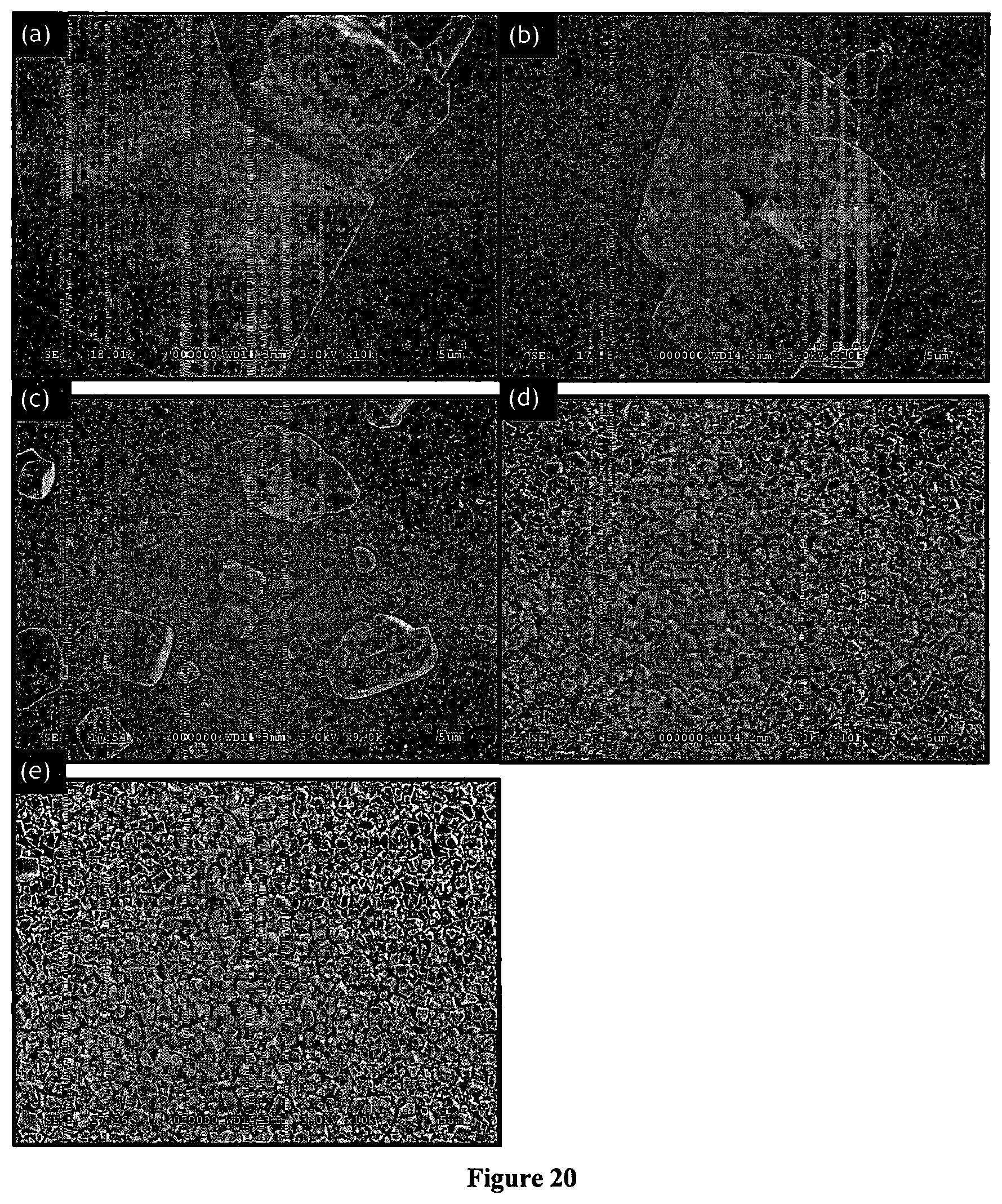
D00017

D00018

D00019

M00001

XML
uspto.report is an independent third-party trademark research tool that is not affiliated, endorsed, or sponsored by the United States Patent and Trademark Office (USPTO) or any other governmental organization. The information provided by uspto.report is based on publicly available data at the time of writing and is intended for informational purposes only.
While we strive to provide accurate and up-to-date information, we do not guarantee the accuracy, completeness, reliability, or suitability of the information displayed on this site. The use of this site is at your own risk. Any reliance you place on such information is therefore strictly at your own risk.
All official trademark data, including owner information, should be verified by visiting the official USPTO website at www.uspto.gov. This site is not intended to replace professional legal advice and should not be used as a substitute for consulting with a legal professional who is knowledgeable about trademark law.