Device for detecting and illuminating the vasculature using an FPGA
Zott , et al. Feb
U.S. patent number 10,568,518 [Application Number 15/679,277] was granted by the patent office on 2020-02-25 for device for detecting and illuminating the vasculature using an fpga. This patent grant is currently assigned to AccuVein, Inc.. The grantee listed for this patent is AccuVein, Inc.. Invention is credited to Seung P. Kim, Fred Wood, Dimitry Yavid, Klaus Zietlow, Joseph Zott.


| United States Patent | 10,568,518 |
| Zott , et al. | February 25, 2020 |
Device for detecting and illuminating the vasculature using an FPGA
Abstract
A laser based vascular illumination system utilizing a FPGA for detecting vascular positions, processing an image of such vasculature positions, and projecting the image thereof onto the body of a patient.
| Inventors: | Zott; Joseph (Menlo Park, CA), Wood; Fred (Medford, NY), Yavid; Dimitry (Stony Brook, NY), Kim; Seung P. (San Francisco, CA), Zietlow; Klaus (Piedmont, CA) | ||||||||||
|---|---|---|---|---|---|---|---|---|---|---|---|
| Applicant: |
|
||||||||||
| Assignee: | AccuVein, Inc. (Cold Spring
Harbor, NY) |
||||||||||
| Family ID: | 50026136 | ||||||||||
| Appl. No.: | 15/679,277 | ||||||||||
| Filed: | August 17, 2017 |
Prior Publication Data
| Document Identifier | Publication Date | |
|---|---|---|
| US 20180070832 A1 | Mar 15, 2018 | |
Related U.S. Patent Documents
| Application Number | Filing Date | Patent Number | Issue Date | ||
|---|---|---|---|---|---|
| 14723674 | May 28, 2015 | 9782079 | |||
| 13957767 | Jul 7, 2015 | 9072426 | |||
| 61678726 | Aug 2, 2012 | ||||
| Current U.S. Class: | 1/1 |
| Current CPC Class: | A61B 5/742 (20130101); A61B 5/0082 (20130101); A61B 5/1079 (20130101); A61B 5/745 (20130101); A61B 5/1075 (20130101); A61B 5/743 (20130101); A61B 5/004 (20130101); A61B 5/1077 (20130101); A61B 5/02007 (20130101); A61B 5/0033 (20130101) |
| Current International Class: | A61B 5/00 (20060101); A61B 5/02 (20060101); A61B 5/107 (20060101) |
References Cited [Referenced By]
U.S. Patent Documents
| 3136310 | June 1964 | Meltzer |
| 3349762 | October 1967 | Kapany |
| 3511227 | May 1970 | Stern |
| 3527932 | September 1970 | Thomas |
| 3818129 | June 1974 | Yamamoto |
| 3984629 | October 1976 | Gorog |
| 4030209 | June 1977 | Dreidling |
| 4057784 | November 1977 | Tafoya |
| 4109647 | August 1978 | Stern |
| 4162405 | July 1979 | Chance |
| 4182322 | January 1980 | Miller |
| 4185808 | January 1980 | Donohoe et al. |
| 4213678 | July 1980 | Pomerantzeff |
| 4265227 | May 1981 | Ruge |
| 4312357 | January 1982 | Andersson et al. |
| 4315318 | February 1982 | Kato |
| 4321930 | March 1982 | Jobsis et al. |
| 4393366 | July 1983 | Hill |
| 4495949 | January 1985 | Stoller |
| 4502075 | February 1985 | DeForest et al. |
| 4510938 | April 1985 | Jobsis |
| 4536790 | August 1985 | Kruger |
| 4565968 | January 1986 | Macovski |
| 4567896 | February 1986 | Barnea |
| 4576175 | March 1986 | Epstein |
| 4586190 | April 1986 | Tsuji |
| 4590948 | May 1986 | Nilsson |
| 4596254 | June 1986 | Adrian |
| 4619249 | October 1986 | Landry |
| 4669467 | June 1987 | Willet |
| 4697147 | September 1987 | Moran |
| 4699149 | October 1987 | Rice |
| 4703758 | November 1987 | Omura |
| 4766299 | August 1988 | Tierney et al. |
| 4771308 | September 1988 | Tejima et al. |
| 4780919 | November 1988 | Harrison |
| 4799103 | January 1989 | Mucherheide |
| 4817622 | April 1989 | Pennypacker et al. |
| 4846183 | July 1989 | Martin |
| 4862894 | September 1989 | Fujii |
| 4899756 | February 1990 | Sonek |
| 4901019 | February 1990 | Wedeen |
| 4926867 | May 1990 | Kanda |
| RE33234 | June 1990 | Landry |
| 4938205 | July 1990 | Nudelman |
| 5074642 | December 1991 | Hicks |
| 5088493 | February 1992 | Giannini |
| 5103497 | April 1992 | Hicks |
| 5146923 | September 1992 | Dhawan |
| 5174298 | December 1992 | Dolfi |
| 5184188 | February 1993 | Bull |
| 5214458 | May 1993 | Kenai |
| 5222495 | June 1993 | Clarke |
| 5261581 | November 1993 | Harden |
| 5293873 | March 1994 | Fang |
| 5339817 | August 1994 | Nilsson |
| 5371347 | December 1994 | Plesko |
| 5406070 | April 1995 | Edgar et al. |
| 5418546 | May 1995 | Nakagakiuchi et al. |
| 5423091 | June 1995 | Lange |
| 5436655 | July 1995 | Hiyama |
| D362910 | October 1995 | Creaghan |
| 5455157 | October 1995 | Hinzpeter et al. |
| 5494032 | February 1996 | Robinson |
| 5497769 | March 1996 | Gratton |
| 5504316 | April 1996 | Bridgelall et al. |
| 5519208 | May 1996 | Esparza et al. |
| 5541820 | July 1996 | McLaughlin |
| 5542421 | August 1996 | Erdman |
| 5598842 | February 1997 | Ishihara et al. |
| 5603328 | February 1997 | Zucker et al. |
| 5608210 | March 1997 | Esparza et al. |
| 5610387 | March 1997 | Bard et al. |
| 5625458 | April 1997 | Alfano |
| 5631976 | May 1997 | Bolle et al. |
| 5655530 | August 1997 | Messerschmidt |
| 5678555 | October 1997 | O'Connell |
| 5716796 | February 1998 | Bull |
| 5719399 | February 1998 | Alfano et al. |
| 5747789 | May 1998 | Godik |
| 5756981 | May 1998 | Roustaei et al. |
| 5758650 | June 1998 | Miller |
| 5772593 | June 1998 | Hakamata |
| 5787185 | July 1998 | Clayden |
| 5814040 | September 1998 | Nelson |
| 5836877 | November 1998 | Zavislan |
| 5847394 | December 1998 | Alfano et al. |
| 5860967 | January 1999 | Zavislan et al. |
| 5929443 | July 1999 | Alfano et al. |
| 5946220 | August 1999 | Lemelson |
| 5947906 | September 1999 | Dawson, Jr. et al. |
| 5966204 | October 1999 | Abe |
| 5969754 | October 1999 | Zeman |
| 5982553 | November 1999 | Bloom et al. |
| 5988817 | November 1999 | Mizushima et al. |
| 5995856 | November 1999 | Manheimer et al. |
| 5995866 | November 1999 | Lemelson |
| 6006126 | December 1999 | Cosman |
| 6032070 | February 2000 | Flock et al. |
| 6056692 | May 2000 | Schwartz |
| 6061583 | May 2000 | Ishihara et al. |
| 6101036 | August 2000 | Bloom |
| 6122042 | September 2000 | Wunderman |
| 6132379 | October 2000 | Patacsil |
| 6135599 | October 2000 | Fang |
| 6141985 | November 2000 | Cluzeau et al. |
| 6142650 | November 2000 | Brown et al. |
| 6149644 | November 2000 | Xie |
| 6171301 | January 2001 | Nelson |
| 6178340 | January 2001 | Svetliza |
| 6230046 | May 2001 | Crane et al. |
| 6240309 | May 2001 | Yamashita |
| 6251073 | June 2001 | Imran et al. |
| 6263227 | July 2001 | Boggett et al. |
| 6301375 | October 2001 | Choi |
| 6305804 | October 2001 | Rice |
| 6314311 | November 2001 | Williams et al. |
| 6334850 | January 2002 | Amano et al. |
| 6353753 | March 2002 | Flock |
| 6424858 | July 2002 | Williams |
| 6436655 | August 2002 | Bull |
| 6438396 | August 2002 | Cook et al. |
| 6463309 | October 2002 | Ilia |
| 6464646 | October 2002 | Shalom et al. |
| 6523955 | February 2003 | Eberl |
| 6542246 | April 2003 | Toida |
| 6556854 | April 2003 | Sato et al. |
| 6556858 | April 2003 | Zeman |
| 6599247 | July 2003 | Stetten |
| 6631286 | October 2003 | Pfeiffer |
| 6648227 | November 2003 | Swartz et al. |
| 6650916 | November 2003 | Cook et al. |
| 6689075 | February 2004 | West |
| 6690964 | February 2004 | Bieger et al. |
| 6702749 | March 2004 | Paladini et al. |
| 6719257 | April 2004 | Greene et al. |
| 6755789 | June 2004 | Stringer |
| 6777199 | August 2004 | Bull |
| 6782161 | August 2004 | Barolet et al. |
| 6845190 | January 2005 | Smithwick |
| 6882875 | April 2005 | Crowley |
| 6889075 | May 2005 | Marchitto et al. |
| 6913202 | July 2005 | Tsikos et al. |
| 6923762 | August 2005 | Creaghan |
| 6980852 | December 2005 | Jersey-Willuhn et al. |
| 7092087 | August 2006 | Kumar |
| 7113817 | September 2006 | Winchester |
| 7158660 | January 2007 | Gee et al. |
| 7158859 | January 2007 | Wang |
| 7225005 | May 2007 | Kaufman et al. |
| 7227611 | June 2007 | Hull et al. |
| 7239909 | July 2007 | Zeman |
| 7247832 | July 2007 | Webb |
| 7280860 | October 2007 | Ikeda et al. |
| 7283181 | October 2007 | Allen |
| 7302174 | November 2007 | Tan et al. |
| 7333213 | February 2008 | Kempe |
| D566283 | April 2008 | Brafford et al. |
| 7359531 | April 2008 | Endoh et al. |
| 7376456 | May 2008 | Marshik-Geurts |
| 7431695 | October 2008 | Creaghan |
| 7532746 | May 2009 | Marcotte et al. |
| 7545837 | June 2009 | Oka |
| 7559895 | July 2009 | Stetten |
| 7579592 | August 2009 | Kaushal |
| 7608057 | October 2009 | Woehr et al. |
| 7699776 | April 2010 | Walker et al. |
| 7708695 | May 2010 | Akkermans |
| 7792334 | September 2010 | Cohen |
| 7846103 | December 2010 | Cannon, Jr. |
| 7904138 | March 2011 | Goldman |
| 7904139 | March 2011 | Chance |
| 7925332 | April 2011 | Crane et al. |
| 7966051 | June 2011 | Xie |
| 8032205 | October 2011 | Mullani |
| 8078263 | December 2011 | Zeman et al. |
| 8187189 | May 2012 | Jung et al. |
| 8199189 | June 2012 | Kagenow et al. |
| 8320998 | November 2012 | Sato |
| 8336839 | December 2012 | Boccoleri et al. |
| 8364246 | January 2013 | Thierman |
| 8467855 | June 2013 | Yasui |
| 8494616 | July 2013 | Zeman |
| 8498694 | July 2013 | McGuire, Jr. et al. |
| 8509495 | August 2013 | Xu et al. |
| 8548572 | October 2013 | Crane et al. |
| 8630465 | January 2014 | Wieringa |
| 8649848 | February 2014 | Crane et al. |
| 2001/0006426 | July 2001 | Son |
| 2001/0056237 | December 2001 | Cane |
| 2002/0016533 | February 2002 | Marchitto |
| 2002/0118338 | August 2002 | Kohayakawa |
| 2002/0188203 | December 2002 | Smith |
| 2003/0018271 | January 2003 | Kimble |
| 2003/0052105 | March 2003 | Nagano |
| 2003/0120154 | June 2003 | Sauer |
| 2003/0125629 | July 2003 | Ustuner |
| 2003/0156260 | August 2003 | Putilin |
| 2004/0015158 | January 2004 | Chen et al. |
| 2004/0022421 | February 2004 | Endoh et al. |
| 2004/0046031 | March 2004 | Knowles et al. |
| 2004/0171923 | September 2004 | Kalafut et al. |
| 2004/0222301 | November 2004 | Willins et al. |
| 2005/0017924 | January 2005 | Utt et al. |
| 2005/0033145 | February 2005 | Graham et al. |
| 2005/0043596 | February 2005 | Chance |
| 2005/0047134 | March 2005 | Mueller et al. |
| 2005/0085802 | April 2005 | Gruzdev |
| 2005/0113650 | May 2005 | Pacione et al. |
| 2005/0131291 | June 2005 | Floyd et al. |
| 2005/0135102 | June 2005 | Gardiner et al. |
| 2005/0141069 | June 2005 | Wood et al. |
| 2005/0143662 | June 2005 | Marchitto et al. |
| 2005/0146765 | July 2005 | Turner |
| 2005/0154303 | July 2005 | Walker |
| 2005/0157939 | July 2005 | Arsenault et al. |
| 2005/0161051 | July 2005 | Pankratov et al. |
| 2005/0168980 | August 2005 | Dryden et al. |
| 2005/0174777 | August 2005 | Cooper et al. |
| 2005/0175048 | August 2005 | Stern et al. |
| 2005/0187477 | August 2005 | Serov |
| 2005/0215875 | September 2005 | Khou |
| 2005/0265586 | December 2005 | Rowe et al. |
| 2005/0281445 | December 2005 | Marcotte et al. |
| 2006/0007134 | January 2006 | Ting |
| 2006/0020212 | January 2006 | Xu |
| 2006/0025679 | February 2006 | Viswanathan et al. |
| 2006/0052690 | March 2006 | Sirohey et al. |
| 2006/0081252 | April 2006 | Wood |
| 2006/0100523 | May 2006 | Ogle |
| 2006/0103811 | May 2006 | May et al. |
| 2006/0122515 | June 2006 | Zeman |
| 2006/0129037 | June 2006 | Kaufman et al. |
| 2006/0129038 | June 2006 | Zelenchuk et al. |
| 2006/0151449 | July 2006 | Warner |
| 2006/0173351 | August 2006 | Marcotte et al. |
| 2006/0184040 | August 2006 | Keller et al. |
| 2006/0206027 | September 2006 | Malone |
| 2006/0232660 | October 2006 | Nakajima et al. |
| 2006/0253010 | November 2006 | Brady et al. |
| 2006/0271028 | November 2006 | Altshuler et al. |
| 2007/0016079 | January 2007 | Freeman et al. |
| 2007/0070302 | March 2007 | Govorkov |
| 2007/0115435 | May 2007 | Rosendaal |
| 2007/0176851 | August 2007 | Wiley |
| 2008/0045841 | February 2008 | Wood et al. |
| 2008/0147147 | June 2008 | Griffiths et al. |
| 2008/0194930 | August 2008 | Harris et al. |
| 2009/0018414 | January 2009 | Toofan |
| 2009/0171205 | July 2009 | Kharin |
| 2010/0051808 | March 2010 | Zeman et al. |
| 2010/0061598 | March 2010 | Seo |
| 2010/0087787 | April 2010 | Woehr et al. |
| 2010/0177184 | July 2010 | Berryhill et al. |
| 2010/0312120 | December 2010 | Meier |
| 2014/0039309 | February 2014 | Harris et al. |
| 2014/0046291 | February 2014 | Harris et al. |
| 2289149 | May 1976 | FR | |||
| 1298707 | Dec 1972 | GB | |||
| 1507329 | Apr 1978 | GB | |||
| S60-108043 | Jun 1985 | JP | |||
| 04-042944 | Feb 1992 | JP | |||
| 07-255847 | Oct 1995 | JP | |||
| 08023501 | Jan 1996 | JP | |||
| 08-164123 | Jun 1996 | JP | |||
| 2000/316866 | Nov 2000 | JP | |||
| 2002 328428 | Nov 2002 | JP | |||
| 2002/345953 | Dec 2002 | JP | |||
| 2004 237051 | Aug 2004 | JP | |||
| 2004/329786 | Nov 2004 | JP | |||
| 2003/0020152 | Nov 2004 | KR | |||
| WO 1994 22370 | Oct 1994 | WO | |||
| WO 1996 39925 | Dec 1996 | WO | |||
| WO 9826583 | Jun 1998 | WO | |||
| WO 99/48420 | Sep 1999 | WO | |||
| WO 2001 82786 | Nov 2001 | WO | |||
| WO 2003 009750 | Feb 2003 | WO | |||
| WO 2005/053773 | Jun 2005 | WO | |||
| WO 2007078447 | Jul 2007 | WO | |||
Other References
|
Wiklof, Chris, "Display Technology Spawns Laser Camera," LaserFocusWorld, Dec. 1, 2004, vol. 40, Issue 12, PennWell Corp., USA. cited by applicant . Nikbin, Darius, "IPMS Targets Colour Laser Projectors," Optics & Laser Europe, Mar. 2006, Issue 137, p. 11. cited by applicant . http://sciencegeekgirl.wordpress, com/category/science-myths/page/2/ Myth 7: Blood is Blue. cited by applicant . http://www exploratorium.edu/sports/hnds_up/hands6.html "Hands Up! To Do & Notice: Getting the Feel of Your Hand". cited by applicant . http://www.wikihow.com/See-Blood-Veins-in-Your-Hand-With-a-Flashlight "How to See Blood Veins in Your Hand With a Flashlight". cited by applicant. |
Primary Examiner: Kish; James M
Attorney, Agent or Firm: O'Rourke; Thomas A. Bodner & O'Rourke, LLP
Parent Case Text
CROSS REFERENCE TO RELATED APPLICATIONS
This application is a continuation of U.S. application Ser. No. 14/723,674, filed on May 28, 2015, which is a continuation of U.S. application Ser. No. 13/957,767, filed on Aug. 2, 2013, now issued as U.S. Pat. No. 9,072,426, which claims priority on U.S. Provisional Application Ser. No. 61/678,726, filed on Aug. 2, 2012, with the disclosures of each incorporated herein by reference.
Claims
What is claimed is:
1. An image capture device configured to detect, process, and project an image using a field programmable gate array (FPGA), said image capture device comprising: a first laser configured to output a beam of light at an infrared wavelength; a second laser configured to output a beam of light at a visible red wavelength; a combiner configured to combine said beams of light from said first and second lasers into a co-axial beam of light; an x-direction mirror configured to reflect said coaxial beam of light, and to be pivotable about a first axis, in a first direction and in a second direction; an x-direction mirror driver configured to drive said x-direction mirror to oscillate about said first axis, to cyclically reflect said coaxial beam of light in a line, in both said first and second directions; a y-direction mirror configured to reflect said line of light received from said x-direction mirror, and to be pivotable about a second axis, in a third direction and a fourth direction; a y-direction mirror driver configured to drive said y-direction mirror to oscillate about said second axis; a FPGA configured to control said x-direction mirror driver and said y-direction mirror driver to control said oscillations about said first and second axes to form a pattern of said red and infrared wavelengths of light; a feedback means configured for detecting a position of said x-direction mirror and said y-direction mirror, and for signaling said positions to said FPGA; a photodiode configured to receive the image formed from said infrared light, said photodiode further configured to convert the received image into an analog signal; wherein said second laser driver is further configured to receive said analog signal, and to drive said red laser to project the image using said analog signal; a line correlator configured to measure a shift in convergence between said line of light in said first direction and said second direction, for each said oscillation of said X-direction mirror; a mirror convergence control configured to receive said measured shift in convergence from said line correlator, and to adjust said control of said first mirror driver by said FPGA, for said line in said first direction to converge with said line in said second direction.
2. The image capture device according to claim 1, further comprising: a second feedback means configured for detecting said output of said first and second lasers, and for signaling said detected output to said FPGA, for said FPGA to control said output of said first and second lasers.
3. The image capture device according to claim 2, further comprising: an analog-to-digital converter configured to receive said analog signal from said photodiode, and to convert said analog signal into a digital image signal, and to communicate said digital image signal to said FPGA; wherein said FPGA is configured to receive and process said digital image signal and to output a processed image signal; and wherein said second laser driver is further configured to receive said processed image signal from said FPGA, and to drive said red laser to project said processed image using said x-direction mirror and said y-direction mirror.
4. The image capture device according to claim 3, wherein said photodiode comprises a top photodiode and a bottom photodiode each configured to receive a full frame of the image and to output a respective said analog signal.
5. The image capture device according to claim 4, further comprising: a top front end circuit and a bottom front end circuit, each configured to respectively receive said analog signals of said top and bottom photodiodes; said top and bottom front end circuits configured to control analog filtering, gain, and threshold of said respective analog signals; wherein said analog-to-digital converter comprises a top analog-to-digital converter (ADC) and a bottom ADC configured to respectively receive said analog signals from said top and bottom front end circuits, and to convert said analog signals into respective digital image signals, and to communicate said respective digital image signals to said FPGA; said FPGA further configured to receive each of said respective digital image signals from said top and bottom ADC, and to perform imaging processing within each of said respective images, to form respective enhanced images; wherein said FPGA is further configured to form a single enhanced image signal from said respective enhanced images; and wherein said second laser driver is further configured to receive said single enhanced image from said FPGA, and to drive said red laser to project said enhanced single image using said x-direction mirror and said y-direction mirror.
6. The image capture device according to claim 5, wherein said single enhanced image is formed from: a merged signal formed by merging said respective digital image signals; or a selected best image signal selected from either of said respective digital image signals.
7. The image capture device according to claim 5, further comprising: a top histogram generator and a bottom histogram generator, each of said top and bottom histogram generators configured to generate a respective histogram of characteristics of said analog signals from said top and bottom photodiodes; and wherein said FPGA is further configured to receive and use said respective histograms to signal said infrared laser driver to adjust power to said infrared laser on a frame by frame basis until said histograms indicate a proper image.
8. The image capture device according to claim 7, wherein said histogram characteristics comprise contrast and intensity levels.
9. The image capture device according to claim 7, further comprising a CPLD configured to control an LCD to display an operating status of said system thereon.
10. The image capture device according to claim 9, wherein said CPLD is further configured to control an audio output to provide audible tones to a user.
11. The image capture device according to claim 10, wherein said CPLD is further configured to control one or more switches on said system for turning on and off said system, for selecting one or more user modes, and for entering data therein.
12. The image capture device according to claim 2, further comprising a microprocessor configured to redundantly receive and monitor said feedback signal for said first and second lasers, and said feedback signal for said X-direction mirror and Y-direction mirror, in conjunction with said FPGA.
13. An image capture device comprising: means for outputting and scanning a beam of light comprising an infrared wavelength and a visible red wavelength in a first and a second direction, for forming respective lines in said first and second directions, and for scanning said lines in a third direction and a fourth direction; a field programmable gate array (FPGA) configured to control said means for outputting and scanning to control said scanning in said first and second directions, and to control said scanning in said third and fourth directions, to form a pattern; a photodiode configured to receive an image formed from said scanned pattern of said infrared wavelength of light, said photodiode further configured to convert the image into an analog signal; wherein said means for outputting and scanning is further configured to receive said analog signal, and to scan said image using said visible red wavelength; a line correlator configured to measure a shift in convergence between said respective lines in said first and second directions; a mirror convergence control configured to receive said measured shift in convergence from said line correlator, and to adjust said control of said means for outputting and scanning by said FPGA, for said line in said first direction to converge with said line in said second direction.
14. The image capture device according to claim 13, further comprising: a first feedback means configured for detecting a position of said x-direction mirror and said y-direction mirror, and for signaling said positions to said FPGA; a second feedback means configured for detecting said output of said means for outputting and scanning, and for signaling said detected output to said FPGA, for said FPGA to control said output of said means for outputting and scanning; an analog-to-digital converter configured to receive said analog signal from said photodiode, and to convert said analog signal into a digital image signal, and to communicate said digital image signal to said FPGA; wherein said FPGA is configured to receive and process said digital image signal and to output a processed image signal; and wherein said means for outputting and scanning is further configured to receive said processed image from said FPGA, and to scan said processed image using said red wavelength.
15. The image capture device according to claim 13, wherein said photodiode comprises a top photodiode and a bottom photodiode each configured to receive a full frame of said image and to output a respective said analog signal.
16. The image capture device according to claim 15, further comprising: a top front end circuit and a bottom front end circuit, each configured to respectively receive said analog signals of said top and bottom photodiodes; said top and bottom front end circuits configured to control analog filtering, gain, and threshold of said respective analog signals; wherein said analog-to-digital converter comprises a top analog-to-digital converter (ADC) and a bottom ADC configured to respectively receive said analog signals from said top and bottom front end circuits, and to convert said analog signals into respective digital image signals, and to communicate said respective digital image signals to said FPGA; said FPGA further configured to receive each of said respective digital image signals from said top and bottom ADC, and to perform imaging processing within each of said respective images, to form respective enhanced images; wherein said FPGA is further configured to form a single enhanced digital image from said respective enhanced images; and wherein said means for outputting and scanning is further configured to receive said single enhanced image from said FPGA, and to scan said single enhanced image using said visible red wavelength.
17. The image capture device according to claim 16, wherein said single enhanced image comprises: a merged signal formed by merging said respective digital image signals; or a selected best image signal selected from either of said respective digital image signals.
18. The image capture device according to claim 16, further comprising: a top histogram generator and a bottom histogram generator, each of said top and bottom histogram generators configured to generate a respective histogram of characteristics of said analog signals from said top and bottom photodiodes; and wherein said FPGA is further configured to receive and use said respective histograms to adjust power to said means for outputting and scanning on a frame by frame basis until said histograms indicate a proper image.
19. The image capture device according to claim 18, wherein said histogram characteristics comprise contrast and intensity levels.
20. The image capture device according to claim 13, further comprising a microprocessor configured to redundantly monitor and control said means for outputting and scanning to control said scanning in said first and second directions, and said scanning in said third and fourth directions, to form a raster pattern.
21. An image capture device comprising: means for outputting and scanning a beam of light comprising an infrared wavelength and a visible red wavelength in a first and a second direction, for forming respective lines in said first and second directions, and for scanning said lines in a third direction and a fourth direction; an electronic component configured to control said means for outputting and scanning to control said scanning in said first and second directions, and to control said scanning in said third and fourth directions, to form a pattern; a photodiode configured to receive an image formed from said scanned pattern of said infrared wavelength of light, said photodiode further configured to convert the image into an analog signal; wherein said means for outputting and scanning is further configured to receive said analog signal, and to scan said image using said visible red wavelength; a line correlator configured to measure a shift in convergence between said respective lines in said first and second directions; a mirror convergence control configured to receive said measured shift in convergence from said line correlator, and to adjust said control of said means for outputting and scanning by said electronic component, for said line in said first direction to converge with said line in said second direction.
22. The image capture device according to claim 21, further comprising: a feedback means configured for detecting said output of said means for outputting and scanning, and for signaling said detected output to said electronic component, for said electronic component to control said output of said means for outputting and scanning; an analog-to-digital converter configured to receive said analog signal from said photodiode, and to convert said analog signal into a digital image signal, and to communicate said digital image signal to said electronic component; wherein said electronic component is configured to receive and process said digital image signal and to output a processed image signal; and wherein said means for outputting and scanning is further configured to receive said processed image from said electronic component, and to scan said processed image using said red wavelength.
23. The image capture device according to claim 22, wherein said photodiode comprises a top photodiode and a bottom photodiode each configured to receive a full frame of said image and to output a respective said analog signal.
Description
BACKGROUND
Summary
A laser based vascular illumination system utilizing a FPGA for detecting vascular positions, processing an image of such vasculature positions, and projecting the image thereof onto the body of a patient.
BRIEF DESCRIPTION
FIG. 1 Block diagram of a system for detecting and illuminating the vasculature in a patient.
FIG. 2 Shows the signal processing flow of the FPGA.
FIG. 3 shows the internal bus architecture of the FPGA.
FIG. 4 shows details of the vein processing.
FIG. 5 shows the vein processing at the boundary of the image frames.
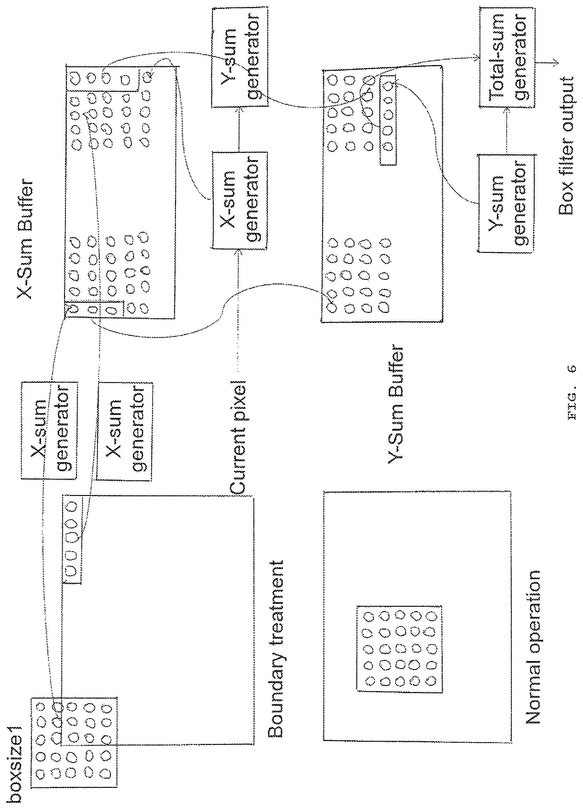
FIG. 6 shows further detail of the vein processing at the boundary of the image frames.
FIG. 7 2-D Moving Window Sum Generator.
FIG. 8 shows a X-sum generator.
DETAILED DESCRIPTION
FIG. 1 shows a block diagram of a system for detecting and illuminating the vasculature in a patient.
The system shown in the block diagram of FIG. 1 is used for detecting the location of veins on a patient and illuminating the veins.
The disclosures of U.S. patent application Ser. No. 12/804,506, now issued as U.S. Pat. No. 8,463,364 are incorporated herein by reference.
In a preferred embodiment, FIGS. 30-47 of application Ser. No. 12/804,506 illustrates an assembly of a housing that may be used in the present invention. In the present invention, circuit boards 43, 44 and 15 of application Ser. No. 12/804,506 may be modified to contain the circuitry described by the block diagram in FIG. 1. The remainder of the device in FIGS. 30-47 can remain substantially the same.
In FIG. 1 an FPGA 1 (field programmable gate array) is configured to control a red laser drive 2 which in turn drives a red laser 3. The output of the red laser 3 is controlled in a manner so as to illuminate the detected veins. A red laser feedback 4 detects the output of the red laser 3 and sends the information to the FPGA 1. Accordingly, a closed loop is formed whereby the FPGA 1 can both drive the Red laser 3 and receive feedback as to the red laser 3 state.
FPGA 1 outputs data to an IR laser drive 5 which in turn drives an IR laser 6. The output of the IR laser 6 is controlled to output an intensity of IR light, aimed at the area of the body where veins are located, sufficient to detect the veins. An IR laser feedback 7 detects the output of the IR laser 6 and sends the information to the FPGA 1. Accordingly, a closed loop is formed whereby the FPGA 1 can both drive the IR Laser 6 and receive feedback as to the IR laser 6 state.
FPGA 1 communicates to both a x-mirror drive 8 and a y-mirror drive 9 to drive x-mirror 10 and y-mirror 11 in such a manner that a raster pattern is formed on the patient when the Red laser 3 and the IR laser 6 are coaxially projected thereon. X-mirror feedback 12 and y-mirror feedback 13 detect the positions of the x-mirror 10 and y-mirror 11, respectively, and communicates such information to the FPGA1.
Top photodiode 23 and bottom photodiode 22 receive the IR Laser 6 reflected off the patient, converts the light into an analog signal which is provided to Top FE 25 and Bottom FE 24, and then to Top ADC 27 and bottom ADC 25, respectively. The top FE 25 and the bottom FE 24 are front end circuits that provide analog filtering, gain control and threshold of the analog signals. The Top ADC 27 and bottom ADC 26 are analog to digital converters that convert the analog signals to digital representations thereof to be communicated to the FPGA 1. Control lines are provided from the FPGA 1 to the top FE 25 and the bottom FE 24 to set parameters such as, for example, gain control and analog filtering.
From a mechanical standpoint, the red laser 3 and the IR laser 6 are co axially aligned and projected off of mirrors X-mirror 10 and Y-mirror 11 to form a pattern, such as for example, a raster pattern on the patient. The IR laser 6 reflects off the patient and is received by top photodiode 23 and photodiode 22. The reflected IR light contains information as to the location of the veins (IR light is absorbed by the blood in the veins and therefore the amount or reflected IR light is lower when the IR laser 6 is aimed at a vein. The FPGA 1 time sequentially receives in the signal form the top ADC 27 and the bottom ADC and can form two partial and/or full frame images of the reflected IR light (hereinafter a top channel data and a bottom channel data wherein the top channel data is received from the top ADC 27 and the bottom channel data is received from the bottom ADC). The FPGA 1 processes one or both of the partial and/or full image to detect and enhance the image of the veins. The enhanced image is time sequentially projected by the Red laser 3 onto the patient.
A CPLD is provided for controlling an LCD 19 with displays user information related to the operating status of the device. It also controls an audio 20 output to provide audible tones to the user. Finally the CPLD 18 controls the switches 21 on the unit for turning on and off the units as well as selecting user modes and entering data.
A microprocessor PIC MCU 17 is provided for receiving and monitoring the IR laser feedback 7 signal, the red laser feedback 4 signal, the x-mirror feedback 12 signal and the y-mirror feedback 13 signal. Since these signals are also provided to the FPGA 1, redundancy monitoring of the signals is provided by the PIC MCU 17. This is particularly important when regulatory requirements require redundant monitoring of the laser power and movement to comply with safety requirements. The PIC MCU 17 also monitors the device power management 14, the Li-ion Battery management 15 circuitry and the Li-ion Fuel gauge 16.
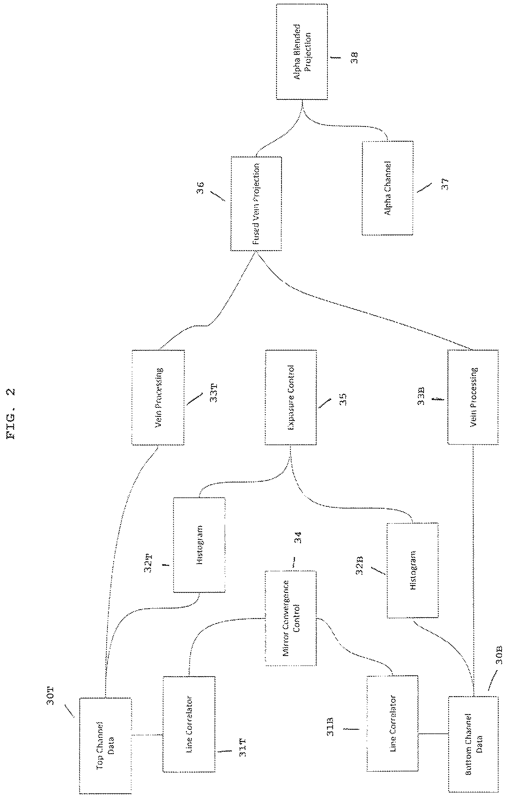
FIG. 2 shows an example of the signal processing flow of the FPGA.
FIG. 2 shows an embodiment of the signal processing algorithm of the FPGA of FIG. 1. As described with reference to FIG. 1, the image of the reflected IR laser 6 is time sequentially stored in the FPGA 1 as top channel data 30T and bottom channel data 30B.
The X-mirror 10 oscillates about a single axis to move the laser beam from the IR laser 6 to form a line. The beam moves first in one direction and then back in the other direction. It is critical that the left to right image data be in convergence with the right to left data. The top line correlator 31T measures the shift in the convergence of the top channel data 30T and supplies the information to the mirror convergence control 34. Similarly, the bottom line correlator 31B measures the shift in the convergence of the bottom channel data 30B and supplies the information to the mirror convergence control 34. The mirror convergence control 34 can adjust the control signals provided from the FPGA 1 to the x-mirror drive 8 so as to converge the data.
A top histogram 32T receives the top channel data 30T and generates a histogram based upon an entire frame of the top channel data 30T. Similarly, a bottom histogram 32B receives the top channel data 30B and generates a histogram based upon an entire frame of the bottom channel data 30B. The histograms contain information describing the characteristics of the images, including but not limited to contrast and intensity levels. The top histogram 32T and the bottom histogram 32B are provided to exposure control 35. Exposure control 35 communicates appropriate signals the IR laser drive 5 to adjust the power of the IR laser 6 on a frame by frame basis until the histograms indicate appropriate images. The exposure control 35 also communicates with the top FE 25 and bottom FE 24 to adjust parameters such as setting thresholds and setting electrical gain.
A top vein processing 33T block receives the top channel data 30T and performs image processing to detect vein patterns and provides the enhanced vein image to fused vein projection 36. Similarly, bottom vein processing 33B block receives the bottom channel data 30B and performs image processing to detect vein patterns and provides the enhanced vein image to fused vein projection 36. The fused vein projection 36 forms a single image and communicates the image to the alpha blended projection 38. The fused vein projection 36 can form the single image by merging the images from the top vein processing 33T and bottom vein processing 33B. Alternative, the fused vein projection 36 can simply select the best image received from the top vein processing 33T and the bottom vein processing 33B.
Alpha channel 37 forms an image that contains graphical data, such as text or characters. Alpha channel 37 and fused vein projection 36 are provided to alpha blended projection 38 with drives the IR laser drive 5 to display an image which is the combination of the fused vein projection 36 and the alpha channel 37.
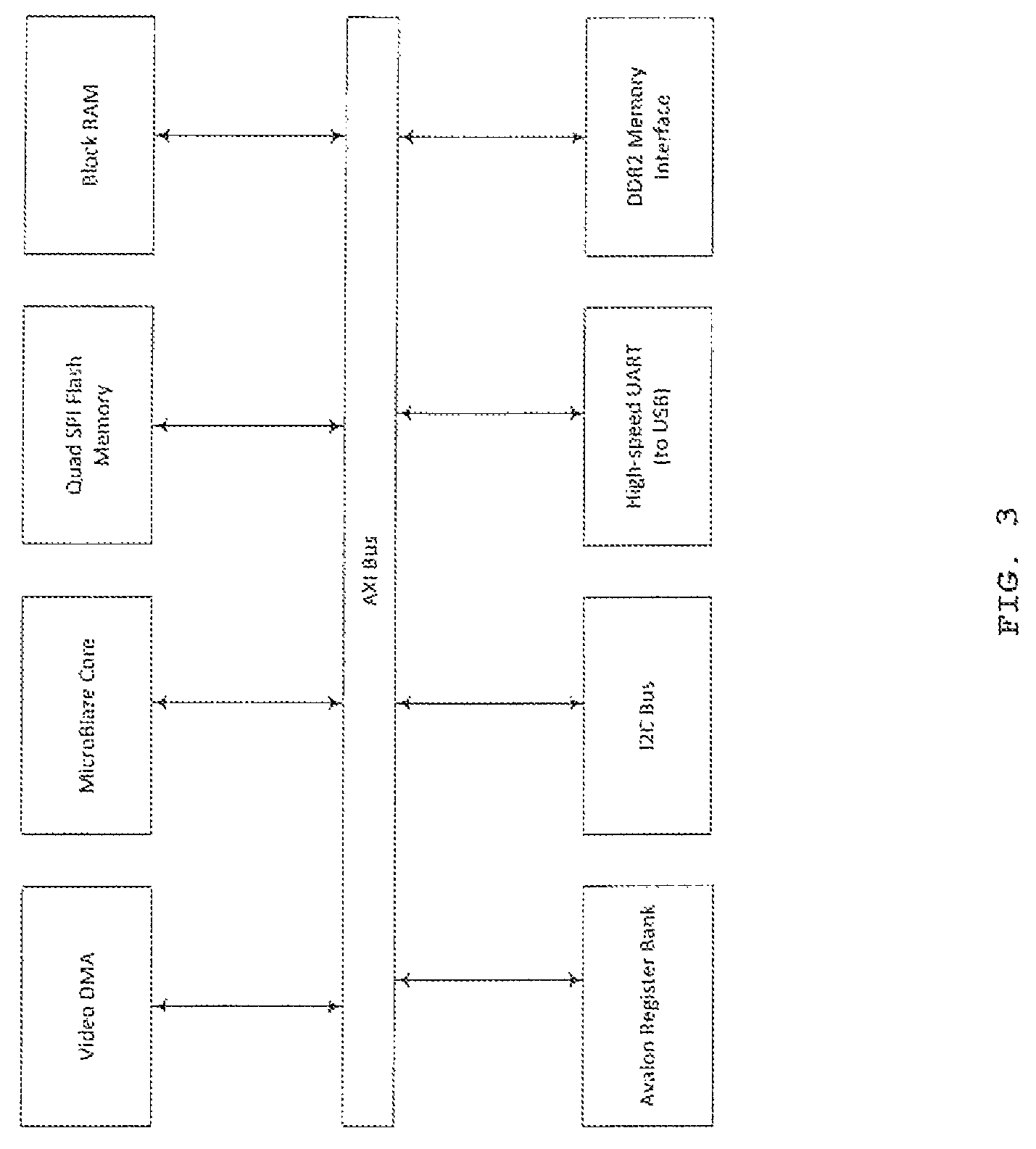
FIG. 3 shows an example of the internal bus architecture of the FPGA
FIG. 4 shows details of the top vein processing 33T and bottom vein processing 33B.
FIG. 5 shows the vein processing at the boundary of the image frames.
FIG. 6 shows further detail of the vein processing at the boundary of the image frames.
FIG. 7 shows the 2-D Moving Window Sum Generator.
FIG. 8 shows a X-sum generator.
* * * * *
References
D00000
D00001
D00002
D00003
D00004
D00005
D00006
D00007
D00008
XML
uspto.report is an independent third-party trademark research tool that is not affiliated, endorsed, or sponsored by the United States Patent and Trademark Office (USPTO) or any other governmental organization. The information provided by uspto.report is based on publicly available data at the time of writing and is intended for informational purposes only.
While we strive to provide accurate and up-to-date information, we do not guarantee the accuracy, completeness, reliability, or suitability of the information displayed on this site. The use of this site is at your own risk. Any reliance you place on such information is therefore strictly at your own risk.
All official trademark data, including owner information, should be verified by visiting the official USPTO website at www.uspto.gov. This site is not intended to replace professional legal advice and should not be used as a substitute for consulting with a legal professional who is knowledgeable about trademark law.