Power line signal coupler
Olmstead , et al. Feb
U.S. patent number 10,560,154 [Application Number 16/189,799] was granted by the patent office on 2020-02-11 for power line signal coupler. This patent grant is currently assigned to ESKER TECHNOLOGIES, LLC. The grantee listed for this patent is Esker Technologies, LLC. Invention is credited to Brian S. Olmstead, Brad Rake.


| United States Patent | 10,560,154 |
| Olmstead , et al. | February 11, 2020 |
Power line signal coupler
Abstract
A main power line (+ and - lines) is coupled to a power supply, for example a car battery, grounded to a vehicle chassis. Positive and negative main power lines are coupled to a power line gateway module, and spliced to carry power for a segment, until receiving, by splices, RF power line communications. The main power lines, now carrying power and RF power line communications are then coupled to remote modules. RF power line communication carries signal from the power line gateway module to a impedance matching network or a transformer are used to match impedances.
| Inventors: | Olmstead; Brian S. (Bayside, WI), Rake; Brad (Hubertus, WI) | ||||||||||
|---|---|---|---|---|---|---|---|---|---|---|---|
| Applicant: |
|
||||||||||
| Assignee: | ESKER TECHNOLOGIES, LLC
(Mequon, WI) |
||||||||||
| Family ID: | 65720839 | ||||||||||
| Appl. No.: | 16/189,799 | ||||||||||
| Filed: | November 13, 2018 |
Prior Publication Data
| Document Identifier | Publication Date | |
|---|---|---|
| US 20190089411 A1 | Mar 21, 2019 | |
Related U.S. Patent Documents
| Application Number | Filing Date | Patent Number | Issue Date | ||
|---|---|---|---|---|---|
| 15646266 | Nov 13, 2018 | 10128906 | |||
| 62360785 | Jul 11, 2016 | ||||
| Current U.S. Class: | 1/1 |
| Current CPC Class: | H04B 3/56 (20130101); H04B 3/548 (20130101); H04B 2203/5487 (20130101); H04B 2203/5491 (20130101); H04B 2203/5425 (20130101) |
| Current International Class: | H04B 3/56 (20060101); H04B 3/54 (20060101) |
| Field of Search: | ;340/310.01,428,431,532,533,538,538.1 ;307/1,9.1,150 ;317/61.5 |
References Cited [Referenced By]
U.S. Patent Documents
| 2990482 | June 1961 | Morris |
| 2996652 | August 1961 | Cassell |
| 3139585 | June 1964 | Ross |
| 3678341 | July 1972 | Constable |
| 4523307 | June 1985 | Brown et al. |
| 4639609 | January 1987 | Floyd et al. |
| 4749992 | June 1988 | Fitzemeyer et al. |
| 4823383 | April 1989 | Cardot et al. |
| 5040168 | August 1991 | Maue et al. |
| 5142278 | August 1992 | Moallemi et al. |
| 5148144 | September 1992 | Sutterlin et al. |
| 5353189 | October 1994 | Tomlinson |
| 5488352 | January 1996 | Jasper |
| 5694109 | December 1997 | Nguyen |
| 5727025 | March 1998 | Maryanka |
| 5739592 | April 1998 | Rigsby et al. |
| 5745027 | April 1998 | Malville |
| 5812557 | September 1998 | Stewart et al. |
| 5870016 | February 1999 | Shrestha |
| 5900803 | May 1999 | Politz et al. |
| 6006143 | December 1999 | Bartel et al. |
| 6127939 | October 2000 | Lesesky et al. |
| 6137880 | October 2000 | Bella |
| 6167121 | December 2000 | Arai |
| 6229432 | May 2001 | Fridley et al. |
| 6229434 | May 2001 | Knapp et al. |
| 6356426 | March 2002 | Dougherty |
| 6373377 | April 2002 | Sacca et al. |
| 6392368 | May 2002 | Deller et al. |
| 6393064 | May 2002 | Nagai et al. |
| 6400103 | June 2002 | Adamson |
| 6411203 | June 2002 | Lesesky et al. |
| 6418221 | July 2002 | Snow et al. |
| 6434459 | August 2002 | Wong et al. |
| 6453687 | September 2002 | Sharood et al. |
| 6507158 | January 2003 | Wang |
| 6512307 | January 2003 | Ilg |
| 6608554 | August 2003 | Lesesky et al. |
| 6629032 | September 2003 | Akiyama |
| 6731201 | May 2004 | Bailey et al. |
| 6744352 | June 2004 | Lesesky et al. |
| 6759946 | July 2004 | Sahinoglu et al. |
| 6771774 | August 2004 | Phan et al. |
| 6799814 | October 2004 | Lesesky et al. |
| 6800957 | October 2004 | Nerone et al. |
| 6842108 | January 2005 | Akiyama et al. |
| 6842668 | January 2005 | Carson et al. |
| 6853724 | February 2005 | Wang |
| 6895089 | May 2005 | Wang |
| 6933752 | August 2005 | Dreps |
| 6970772 | November 2005 | Radtke et al. |
| 7010050 | March 2006 | Maryanka |
| 7042339 | May 2006 | Bruccoleri et al. |
| 7117272 | October 2006 | Rimboim |
| 7245201 | July 2007 | Kline |
| 7286044 | October 2007 | Yanagida et al. |
| 7307520 | December 2007 | Lamon et al. |
| 7545178 | June 2009 | Hung |
| 7741960 | June 2010 | Hoogenakker et al. |
| 7752472 | July 2010 | Diab |
| 7852206 | December 2010 | Yanagida et al. |
| 7859397 | December 2010 | Lamon et al. |
| 7921308 | April 2011 | Dhuyvetter |
| 7973661 | July 2011 | Garg |
| 8154150 | April 2012 | Sakai |
| 8154153 | April 2012 | Yang et al. |
| 8179655 | May 2012 | Wedley |
| 8244177 | August 2012 | Zyambo |
| 8442127 | May 2013 | Stadelmeier et al. |
| 8527135 | September 2013 | Lowrey et al. |
| 8541903 | September 2013 | Burk |
| 8594314 | November 2013 | Kitchin et al. |
| 8638216 | January 2014 | Lamon et al. |
| 8693151 | April 2014 | Iwasa et al. |
| 9451655 | September 2016 | Wong |
| 9515747 | December 2016 | Soto et al. |
| 9537644 | January 2017 | Jones |
| 9672186 | June 2017 | Desposito |
| 9779720 | October 2017 | Lee |
| 9787362 | October 2017 | Varadarajan |
| 2002/0079121 | June 2002 | Ryan |
| 2003/0076221 | April 2003 | Akiyama et al. |
| 2004/0258141 | December 2004 | Tustison |
| 2008/0013637 | January 2008 | Kodama |
| 2009/0134718 | May 2009 | Hurst |
| 2010/0061545 | March 2010 | Kitchin et al. |
| 2011/0279935 | November 2011 | Iwasa |
| 2012/0177133 | July 2012 | Oldenkamp |
| 2013/0223293 | August 2013 | Jones |
| 2014/0265551 | September 2014 | Willis |
| 2015/0065039 | March 2015 | Nii |
| 2016/0285314 | September 2016 | Van Neste |
| 2016/0351327 | December 2016 | Shigematsu |
| 2017/0040968 | February 2017 | Igarashi |
| 2017/0093230 | March 2017 | Yundt |
| 2017/0310306 | October 2017 | Tanghe |
| 0659613 | May 1995 | EP | |||
| 1383280 | Jan 2004 | EP | |||
| 02005123960 | May 2005 | JP | |||
| WO02/052745 | Jul 2002 | WO | |||
| WO2004/055994 | Jul 2004 | WO | |||
Other References
|
Office Action dated Aug. 29, 2006 regarding U.S. Appl. No. 11/227,376, 10 pages. cited by applicant . Office Action dated May 8, 2007 regarding U.S. Appl. No. 11/227,376, 8 pages. cited by applicant . Office Action dated Feb. 18, 2010 regarding U.S. Appl. No. 12/001,123, 7 pages. cited by applicant . Office Action dated Oct. 18, 2017 regarding U.S. Appl. No. 15/287,470, 10 pages. cited by applicant . Joe Klinger, Phone Line Basics: Revisited, Mar. 2002, Radio Guide Magazine, accessed from www.jkaudio.com/article_10.htm on Oct. 10, 2017. cited by applicant. |
Primary Examiner: Nguyen; Hung T
Attorney, Agent or Firm: Ryan Kromholz & Manion, S.C.
Parent Case Text
RELATED APPLICATIONS
This application is a continuation-in-part of U.S. patent application Ser. No. 15/646,266, filed 11 Jul. 2017 (now U.S. Pat. No. 10,128,906) which claims the benefit of U.S. Provisional Patent Application Ser. No. 62/360,785, filed 11 Jul. 2016.
Claims
We claim:
1. A method of configuring an electrical circuit comprising: providing a resonant wire segment between a power source and a power line bus; providing a signal transceiver; coupling a first and second amplifier coupled to said signal transceiver, said amplifiers coupled to a switch, said switch coupled to a transformer, said transformer coupled to a resistor, said resistor coupled to at least one of a positive and a negative line emanating from said power source; said positive and said negative lines coupled to a matching network comprising a series of capacitors, said positive and said negative lines coupled to said power line bus; said resonant wire segment coupling at least one of said positive and said negative lines from said power source and said power bus.
2. The method according to claim 1, wherein said resonant wire segment is between approximately 0.5 and 3 meters in length.
3. The method according to claim 1, wherein said resonant wire segment is between approximately 1 and 1.5 meters in length.
4. The method according to claim 1, wherein a second resonant wire segment is provided on at least one of the positive and negative line between said power source and said power line bus.
Description
BACKGROUND OF THE INVENTION
In electrical communications, as with any communications generally, clarity is key. Clarity may be difficult to achieve in a variety of environments in which clear communications are critical. For instance, communications at radio frequencies over direct current (DC) power busses is known. In some instances, however, reliability of such communications is interrupted by environmental noise and/or voltage spikes occurring on the power bus. Accordingly, the art of communications over or along a DC power bus may be enhanced by better filtering techniques.
Inductors are placed in power lines to add impedance to the lines. In this manner, RF signal can be carried by the lines.
SUMMARY OF THE INVENTION
A filter provides enhanced filtering of transient and spurious signals which may otherwise interfere with a communication signal. Such filter may be advantageously used in wired, noisy communication environments, such as communication environments provided on vehicles (e.g., automobiles, airplanes, boats, locomotives).
Systems of the present invention can inject a signal onto a power line a distance from ground. Inductance of a segment of wire is used in place of a discrete inductor.
A main power line (+ and - lines) is coupled to a power supply, for example a car battery, grounded to a vehicle chassis. Positive and negative main power lines are coupled to a power line gateway module, and spliced to carry power for a segment, until receiving, by splices, RF power line communications. The main power lines, now carrying power and RF power line communications are then coupled to remote modules. RF power line communication carries signal from the power line gateway module to an impedance matching network or a transformer are used to match impedances.
BRIEF DESCRIPTION OF THE DRAWINGS
FIG. 1 is a schematic view of circuitry of the present invention;
FIG. 2 is a detail schematic view of the impedance matching network for impedance transformation of the present invention;
FIG. 3 is a power line coupler of the present invention;
FIG. 4 is a DC Power Line Network ("DPN") diagram of the present invention.
DESCRIPTION OF THE PREFERRED EMBODIMENT
Although the disclosure hereof is detailed and exact to enable those skilled in the art to practice the invention, the physical embodiments herein disclosed merely exemplify the invention which may be embodied in other specific structures. While the preferred embodiment has been described, the details may be changed without departing from the invention.
Referring now to FIG. 1, a schematic view of circuitry of the present invention is shown. A battery 12 (for example a car battery, grounded to a vehicle chassis) carries a main power line (+ and - lines 24 and 20, respectively). An optional fuse 14 is provided on the positive line. Coming from the main positive and negative power lines 24 and 20, power lines 24 and 20 are spliced and coupled to module 16, or power line gateway module GW1002 to power the module. RF power line communication signals are provided by module 16, and carried by lines 22 from the module to impedance matching network (for impedance transformation) capacitor network 18 (discussed in FIG. 2 or 3). After impedance matching network 18, lines 22 go through optional fuse, capacitor or other form of wire protection 28, and are spliced with main positive and negative power lines 24 and 20 at splices 26. Splices 26 can comprise, for example, Scotchlok.TM. connectors by The 3M Company. Following the splices 26, the power lines 24 and 20, now carrying DC power (from battery 12) and RF communications (from module 16 GW1002), carry the DC power and RF communications downstream to a module or bank of modules (not shown) to power and control the modules. Splices off of main power lines 24 and 20 can be made to each module until power lines 24 and 20 terminate.
Still referring to FIG. 1, a desired length 32 of power wires 24 and 20 is preferred between the battery 12 and splices 26. In an exemplary embodiment operating at 4.5 MHz frequency, if length 32 was too short, communications issues could arise as length 32 would not provide enough effective inductance. As the length 32 of the conductor (power wires 24 and 20) increases, so too does the inductance. In a preferred embodiment, a roughly 1 .mu.H (microhenry) inductance is desired in a system at impedance of 40 ohms (.OMEGA.), and resistance of 120 ohms. To achieve the desired inductance, the length and diameter of the power wires 24 and 20 can be changed to target the roughly 1 pH level of inductance. In an exemplary embodiment at 4.5 MHz frequency, for #8 wire, a length 32 of the conductor (power wires 24 and 20) is approximately 4' to achieve the desired self inductance of length 32 of the conductor (power wires 24 and 20). It is preferred to provide length 32 of the conductor (power wires 24 and 20) long enough to provide a high enough impedance.
FIG. 2 is a detail schematic view of the impedance matching network 18 for impedance transformation used in the present invention. Wires 22 enter impedance matching network 18 from module 16, into preferably a circuit board with matching capacitors 36 and 38. In an exemplary embodiment, a 12 nF (nanofarad) capacitor 36 is matched with a 2.7 nF capacitor 38 in a first pair (upper in FIG. 2), and another 12 nF capacitor 36 is matched with a 2.7 nF capacitor 38 in a second pair (lower in FIG. 2). Between 2.7 nF capacitors 38, the unit can be center tapped to ground. Optionally, a capacitor 44/resistor 42 series can be provided to reduce a Q Factor. In this context, Q Factor is the bandwidth of the circuit, defined by the reactance of the circuit), and in this application, a lower Q Factor is desired to allow for wide tuning. In an alternate embodiment (not shown), a capacitor 44/resistor 42 series could be provided in module 16 instead of impedance matching network 18. Signal comes out of impedance matching network 18 with communication signals, 180 out of phase, through a matching network through lines 22 running in parallel with lines 24/20, to which lines 22 are spliced at splices 26.
Referring now to FIG. 3, an alternative capacitor arrangement of impedance matching network 18 is shown, with lines 22 entering into the system, and in an exemplary arrangement a first capacitor 48 (1.3 nF for example) is followed by pair of second capacitors 46 (12 nF for example), again optionally followed by capacitor 44/resistor 42 series. Signal comes out of impedance matching network 18 with communication signals, 180 out of phase, through a matching network through lines 22 running in parallel with lines 24/20, to which lines 22 are spliced at splices 26.
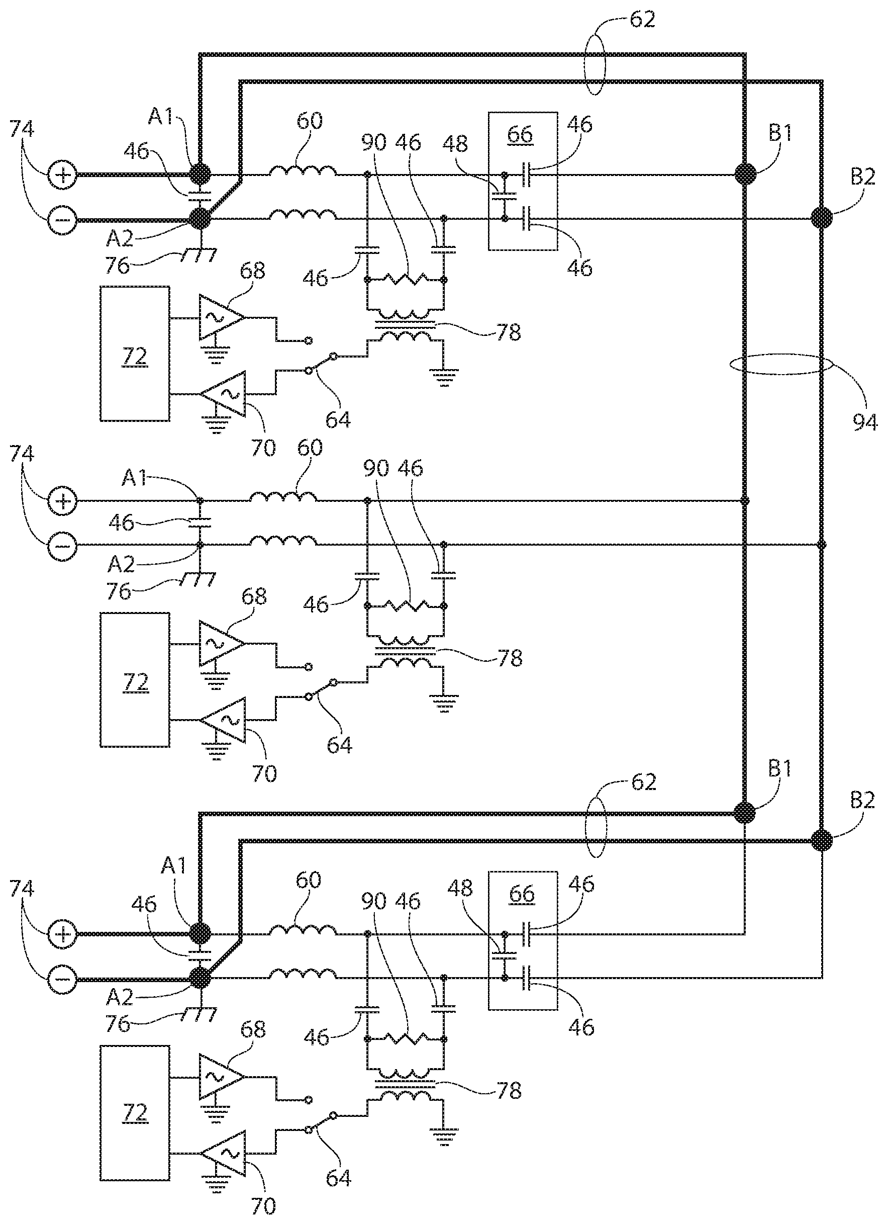
Referring now to FIG. 4, a DC Power Line Network ("DPN") diagram of the present invention is shown. Because discrete inductors become expensive and unwieldy at currents above 30 A, a resonant wire section 62 or sections 62 of preferably between 0.5 and 3 meters are used to provide suitable impedance for signal coupling. Resonant wire sections 62 are more preferably between 0.75 and 2.5 meters, or more preferably between approximately 1 and 1.5 meters, and more preferably yet approximately 1.2 meters long. Additional wire between points B1, B2 and matching networks 66 can add to the inductance of the resonant wire sections 62. In this manner, a reactance of 25 to 30 ohms can be obtained at 4.5 MHz. Matching network 66 cancels the inductive reactance and increases the resistive impedance to prove a good match for the signal transceiver or modules 72.
The DPN physical layer comprises the power line bus 94, analog front end, and radio modem. Another layer can the data link layer which provides data transfer between Modules and CAN-Bus connections. Power source 74 (positive and negative connections) are typically connected to the power line bus 94 through one of the modules 72 and load power may be supplied through any module 72.
Still referring to FIG. 4, modules 72 are shown coupled to transmit amplifier or buffer 68, as well as receiving amplifier 70, both coupled to switch 64. Switch 64 is set to receive in FIG. 4, but can be switched to transmit (bi-directional). Through amplifiers 68 and 70, sine waves are transmitted and received, respectively, through transformer 78, resistors 90 in line and capacitors 46, 48 where indicated. From here, matching network 66 with capacitors 46, 48 are coupled also to points B1 and B2. From points A1 and A2 to points B1 and B2, resonant wire sections 62 are provided of the preferred length as shown. Between points A1, A2 and the matching network 66, inductors 60 are provided, preferably air cored.
Differential signal coupling is provided by a transformer 78 in the DPN system while CAN uses symmetrical transistor drive. To reduce radiated emissions, both systems preferably have passive components to be well matched to minimize common mode voltages on the bus.
Power sources 74 and loads often have a parallel capacitive reactance well below 10 ohms at the DPN carrier frequency. To ensure consistent performance in a variety of installations, inductive devices are used to control the impedance of the DPN-Bus. External termination resistors are not required on the power line bus 94 because one can be included in each module 72.
Although three terminations on the bus 94 are shown in FIG. 4, more or less can be provided. For instance, up to and including eight terminations on the bus 94 could cause some impedance mismatch and signal reflection, but they provide noise damping by absorbing voltage bursts common on power lines. Multiple terminations also reduce communication signal amplitude, but there is adequate operational margin since the receiver is sensitive to a signal 20 dB less than the transmitted signal.
It is also possible to attach any load to the power line bus 94 using a simplified module that does not include a coupling transformer 78 or transceiver when DPN communication is not required. The analog front end (AFE) of the Gateway Module is highly effective at separating data signals from noise. Power line noise is generated by a variety of devices. Passive inductive loads often require no EMC testing but, when wired to the power lines with mechanical switches or relays, they can generate voltage spikes in excess of 500 volts. The AFE blocks these transients and filters them out. Clamping, which binds the upper or lower extreme of a waveform to a fixed DC voltage level, is used sparingly because it will also clamp the communication signal during the event.
Even though voltage transients may contain little energy at the DPN carrier frequency, they could be problematic if filters are not properly designed. Putting a voltage transient into a sharply tuned filter is analogous to striking a mechanical tuning fork with a hammer the filter will ring at the carrier frequency and data will be masked by the internally generated signal.
Because vehicle chassis ground is sometimes used to return load current, the AFE is designed to operate with unbalanced DC currents in power and ground wires with little or no degradation in EMC performance. Also, since a DC bias will cause magnetic saturation of the high permeability ferrite materials in common mode chokes, they cannot be depended upon to balance the DPN carrier signal and are not included in the design.
The radio modem transmits and receives data packets on the power line in a format similar to J1939 CAN-Bus data. Phase modulation, in which data is encoded by varying the phase of the carrier (sine) wave, is used to communicate information. The phase changes modulate a carrier frequency of 4.5 MHz with a 6.5 MHz option. If noise obscures a single phase change during reception, the noise is ignored. This allows improved immunity to short noise spikes.
The foregoing is considered as illustrative only of the principles of the invention. Furthermore, since numerous modifications and changes will readily occur to those skilled in the art, it is not desired to limit the invention to the exact construction and operation shown and described. While the preferred embodiment has been described, the details may be changed without departing from the invention, which is defined by the claims.
* * * * *
References
D00000
D00001
D00002
XML
uspto.report is an independent third-party trademark research tool that is not affiliated, endorsed, or sponsored by the United States Patent and Trademark Office (USPTO) or any other governmental organization. The information provided by uspto.report is based on publicly available data at the time of writing and is intended for informational purposes only.
While we strive to provide accurate and up-to-date information, we do not guarantee the accuracy, completeness, reliability, or suitability of the information displayed on this site. The use of this site is at your own risk. Any reliance you place on such information is therefore strictly at your own risk.
All official trademark data, including owner information, should be verified by visiting the official USPTO website at www.uspto.gov. This site is not intended to replace professional legal advice and should not be used as a substitute for consulting with a legal professional who is knowledgeable about trademark law.