Diode having high brightness and method thereof
Yoo Fe
U.S. patent number 10,553,744 [Application Number 16/167,229] was granted by the patent office on 2020-02-04 for diode having high brightness and method thereof. This patent grant is currently assigned to LG INNOTEK CO., LTD.. The grantee listed for this patent is LG INNOTEK CO., LTD.. Invention is credited to Myung Cheol Yoo.


| United States Patent | 10,553,744 |
| Yoo | February 4, 2020 |
Diode having high brightness and method thereof
Abstract
A light emitting device can include a substrate including first and second surfaces, the substrate having a thickness of less than 350 micrometers; a reflective layer on the second surface of the substrate; a light emitting structure on the first surface of the substrate and including first and second semiconductor layers with an active layer therebetween, the second semiconductor layer includes an aluminum-gallium-nitride layer, and the active layer includes aluminum and indium and has a multiple quantum well layer; a transparent conductive layer disposed on the second semiconductor layer and including an indium-tin-oxide; a first electrode on the first semiconductor layer and including multiple layers; a second electrode on the transparent conductive layer and including multiple layers; first and second pads on the first and second electrodes, respectively, in which the second pad includes the same material as the first pad and has a thickness of more than 500 nanometers.
| Inventors: | Yoo; Myung Cheol (Pleasanton, CA) | ||||||||||
|---|---|---|---|---|---|---|---|---|---|---|---|
| Applicant: |
|
||||||||||
| Assignee: | LG INNOTEK CO., LTD. (Seoul,
KR) |
||||||||||
| Family ID: | 25421760 | ||||||||||
| Appl. No.: | 16/167,229 | ||||||||||
| Filed: | October 22, 2018 |
Prior Publication Data
| Document Identifier | Publication Date | |
|---|---|---|
| US 20190058083 A1 | Feb 21, 2019 | |
Related U.S. Patent Documents
| Application Number | Filing Date | Patent Number | Issue Date | ||
|---|---|---|---|---|---|
| 15457655 | Mar 13, 2017 | 10147841 | |||
| 14807632 | May 2, 2017 | 9640713 | |||
| 14185620 | Sep 15, 2015 | 9136424 | |||
| 13074566 | Mar 18, 2014 | 8674386 | |||
| 12461681 | May 10, 2011 | 7939849 | |||
| 11247225 | Sep 1, 2009 | 7582912 | |||
| 09905969 | Jun 27, 2006 | 7067849 | |||
| Current U.S. Class: | 1/1 |
| Current CPC Class: | H01L 33/12 (20130101); H01L 33/22 (20130101); H01L 33/62 (20130101); H01L 33/387 (20130101); H01L 33/06 (20130101); H01L 33/483 (20130101); H01L 33/405 (20130101); H01L 33/32 (20130101); H01L 33/46 (20130101); H01L 33/42 (20130101); H01L 33/0025 (20130101); H01L 25/0753 (20130101) |
| Current International Class: | H01L 33/00 (20100101); H01L 33/62 (20100101); H01L 33/40 (20100101); H01L 25/075 (20060101); H01L 33/42 (20100101); H01L 33/12 (20100101); H01L 33/46 (20100101); H01L 33/06 (20100101); H01L 25/07 (20060101); H01L 33/32 (20100101); H01L 33/22 (20100101); H01L 33/48 (20100101); H01L 33/38 (20100101) |
| Field of Search: | ;257/211 |
References Cited [Referenced By]
U.S. Patent Documents
| 4236296 | December 1980 | Woolhouse et al. |
| 4704369 | November 1987 | Nath et al. |
| 5103269 | April 1992 | Tomomura et al. |
| 5132750 | July 1992 | Kato et al. |
| 5369289 | November 1994 | Tamaki et al. |
| 5514903 | May 1996 | Inoue et al. |
| 5593815 | January 1997 | Ahn |
| 5798536 | August 1998 | Tsutsui |
| 5798537 | August 1998 | Nitta |
| 5841802 | November 1998 | Whiteley et al. |
| 5880486 | March 1999 | Nakamura et al. |
| 5904548 | May 1999 | Orcutt |
| 5939735 | August 1999 | Tsutsui et al. |
| 5952681 | September 1999 | Chen |
| 5977566 | November 1999 | Okazaki et al. |
| 6017774 | January 2000 | Yuasa et al. |
| 6051503 | April 2000 | Bhardwaj et al. |
| 6057565 | May 2000 | Yoshida et al. |
| 6063527 | May 2000 | Nishikawa et al. |
| 6069021 | May 2000 | Terashima et al. |
| 6072197 | June 2000 | Horino et al. |
| 6078064 | June 2000 | Ming-Jiunn et al. |
| 6097040 | August 2000 | Morimoto et al. |
| 6121636 | September 2000 | Morita et al. |
| 6121638 | September 2000 | Rennie et al. |
| 6130147 | October 2000 | Major et al. |
| 6146916 | November 2000 | Nanishi et al. |
| 6156584 | December 2000 | Itoh et al. |
| 6185238 | February 2001 | Onomura et al. |
| 6194742 | February 2001 | Kern et al. |
| 6211089 | April 2001 | Kim et al. |
| 6242276 | June 2001 | Baek et al. |
| 6242761 | June 2001 | Fujimoto et al. |
| 6249534 | June 2001 | Itoh et al. |
| 6252255 | June 2001 | Ueta et al. |
| 6274399 | August 2001 | Kern et al. |
| 6281524 | August 2001 | Yamamoto et al. |
| 6291257 | September 2001 | Kadota |
| 6360687 | March 2002 | Yanagisawa et al. |
| 6365429 | April 2002 | Kneissl et al. |
| 6375790 | April 2002 | Fenner |
| 6379985 | April 2002 | Cervantes et al. |
| 6388275 | May 2002 | Kano |
| 6404792 | June 2002 | Yamamoto et al. |
| 6448102 | September 2002 | Kneissl et al. |
| 6456638 | September 2002 | Fukunaga |
| 6468902 | October 2002 | Kawai |
| 6486042 | November 2002 | Gehrke et al. |
| 6488767 | December 2002 | Xu et al. |
| 6489250 | December 2002 | Hwang et al. |
| 6492661 | December 2002 | Chien et al. |
| 6504180 | January 2003 | Heremans et al. |
| 6518602 | February 2003 | Yuasa et al. |
| 6526083 | February 2003 | Kneissl et al. |
| 6562648 | May 2003 | Wong et al. |
| 6564445 | May 2003 | Hashimoto et al. |
| 6570186 | May 2003 | Uemura et al. |
| 6576933 | June 2003 | Sugawara et al. |
| 6579802 | June 2003 | Pierson et al. |
| 6580099 | June 2003 | Nakamura et al. |
| 6586149 | July 2003 | Kawamura et al. |
| 6586777 | July 2003 | Yuasa et al. |
| 6597716 | July 2003 | Takatani |
| 6627921 | September 2003 | Wong et al. |
| 6638846 | October 2003 | Iwata et al. |
| 6693352 | February 2004 | Huang et al. |
| 6720583 | April 2004 | Nunoue et al. |
| 6744196 | June 2004 | Jeon |
| 6765232 | July 2004 | Takahashi et al. |
| 6787435 | September 2004 | Gibb et al. |
| 6812071 | November 2004 | Hayashi et al. |
| 6815725 | November 2004 | Sugawara et al. |
| 6819701 | November 2004 | Henrichs |
| 6841802 | January 2005 | Yoo |
| 6869820 | March 2005 | Chen |
| 6939735 | September 2005 | Smith et al. |
| 6949395 | September 2005 | Yoo |
| 7067197 | June 2006 | Michaluk et al. |
| 7067849 | June 2006 | Yoo |
| 7087933 | August 2006 | Takeda et al. |
| 7148520 | December 2006 | Yoo |
| 7205576 | April 2007 | Song et al. |
| 7250638 | July 2007 | Lee et al. |
| 7265392 | September 2007 | Hahn et al. |
| 7291865 | November 2007 | Kojima et al. |
| 7294521 | November 2007 | Yoo |
| 7319247 | January 2008 | Bader et al. |
| 7371597 | May 2008 | Yoo |
| 7384808 | June 2008 | Liu et al. |
| 7462881 | December 2008 | Lee et al. |
| 7498611 | March 2009 | Eitoh et al. |
| 7518153 | April 2009 | Usuda et al. |
| 7563629 | July 2009 | Lee et al. |
| 7566639 | July 2009 | Kohda |
| 7569865 | August 2009 | Lee et al. |
| 7576368 | August 2009 | Lee et al. |
| 7582912 | September 2009 | Yoo |
| 7588952 | September 2009 | Lee et al. |
| 7649210 | January 2010 | Yoo |
| 7682854 | March 2010 | Yoo |
| 7691650 | April 2010 | Yoo |
| 7741653 | June 2010 | Kamei |
| 7772020 | August 2010 | Yoo |
| 7816705 | October 2010 | Lee et al. |
| 7821021 | October 2010 | Yoo |
| 7863638 | January 2011 | Yoo |
| 7875474 | January 2011 | Muraki et al. |
| 7928465 | April 2011 | Lee et al. |
| 7939849 | May 2011 | Yoo |
| 8022386 | September 2011 | Yoo |
| 8106417 | January 2012 | Yoo |
| 8236585 | August 2012 | Yoo |
| 8288787 | October 2012 | Yoo |
| 8294172 | October 2012 | Yoo |
| 8309982 | November 2012 | Hanawa et al. |
| 8368115 | February 2013 | Yoo |
| 8384091 | February 2013 | Yoo |
| 8384120 | February 2013 | Lee et al. |
| 8445921 | May 2013 | Yoo |
| 8502256 | August 2013 | Lee |
| 9640713 | May 2017 | Yoo |
| 10147841 | December 2018 | Yoo |
| 2001/0000335 | April 2001 | Yamada et al. |
| 2001/0010941 | August 2001 | Morita |
| 2001/0023946 | September 2001 | Ueta et al. |
| 2001/0028062 | October 2001 | Uemura et al. |
| 2001/0030316 | October 2001 | Kuramoto et al. |
| 2001/0030329 | October 2001 | Ueta et al. |
| 2001/0041410 | November 2001 | Franz |
| 2002/0037602 | March 2002 | Okada et al. |
| 2002/0117672 | August 2002 | Chu et al. |
| 2002/0117681 | August 2002 | Weeks et al. |
| 2002/0117695 | August 2002 | Borges et al. |
| 2002/0123164 | September 2002 | Slater, Jr. et al. |
| 2002/0137249 | September 2002 | Ishida et al. |
| 2002/0146854 | October 2002 | Koide et al. |
| 2002/0173062 | November 2002 | Chen et al. |
| 2002/0177251 | November 2002 | Ye et al. |
| 2003/0015713 | January 2003 | Yoo |
| 2003/0032297 | February 2003 | Lindstrom et al. |
| 2003/0073321 | April 2003 | Boiteux et al. |
| 2003/0077847 | April 2003 | Yoo |
| 2003/0080344 | May 2003 | Yoo |
| 2003/0122141 | July 2003 | Wong et al. |
| 2003/0151058 | August 2003 | Uemura et al. |
| 2003/0189212 | October 2003 | Yoo |
| 2003/0189215 | October 2003 | Lee et al. |
| 2003/0213969 | November 2003 | Wang et al. |
| 2004/0000672 | January 2004 | Fan et al. |
| 2004/0169181 | September 2004 | Yoo |
| 2004/0169189 | September 2004 | Jeon |
| 2005/0093004 | May 2005 | Yoo |
| 2005/0098792 | May 2005 | Lee et al. |
| 2006/0006400 | January 2006 | Yoo |
| 2006/0027818 | February 2006 | Yoo |
| 2006/0071226 | April 2006 | Kojima et al. |
| 2006/0071230 | April 2006 | Lee et al. |
| 2006/0091420 | May 2006 | Yoo |
| 2006/0094207 | May 2006 | Yoo |
| 2006/0097277 | May 2006 | Yoo |
| 2006/0099730 | May 2006 | Lee et al. |
| 2006/0244001 | November 2006 | Lee et al. |
| 2007/0018173 | January 2007 | Yoo |
| 2007/0057273 | March 2007 | Yoo |
| 2007/0172973 | July 2007 | Yoo |
| 2007/0269913 | November 2007 | Kim et al. |
| 2007/0290224 | December 2007 | Ogawa |
| 2007/0295986 | December 2007 | Lee et al. |
| 2008/0001166 | January 2008 | Lee et al. |
| 2008/0064132 | March 2008 | Yoo |
| 2008/0128733 | June 2008 | Yoo |
| 2008/0182384 | July 2008 | Hata |
| 2009/0008654 | January 2009 | Nagai |
| 2009/0072264 | March 2009 | Yoo |
| 2009/0121241 | May 2009 | Keller et al. |
| 2009/0267100 | October 2009 | Miyake et al. |
| 2009/0278140 | November 2009 | Huang et al. |
| 2009/0278161 | November 2009 | Lee et al. |
| 2010/0012956 | January 2010 | Yoo |
| 2010/0109020 | May 2010 | Yoo |
| 2010/0117096 | May 2010 | Yoo et al. |
| 2010/0127274 | May 2010 | Yoo |
| 2010/0129943 | May 2010 | Yoo |
| 2010/0171125 | July 2010 | Yoo |
| 2010/0207145 | August 2010 | Yoo |
| 2010/0314607 | December 2010 | Yoo |
| 2011/0095331 | April 2011 | Hanawa et al. |
| 2011/0193128 | August 2011 | Lee et al. |
| 2011/0220948 | September 2011 | Yoo |
| 2011/0309400 | December 2011 | Fukushima et al. |
| 2012/0098023 | April 2012 | Weng et al. |
| 2013/0134465 | May 2013 | Yoo |
| 2013/0146928 | June 2013 | Inoue et al. |
| 2013/0240945 | September 2013 | Aoki et al. |
| 2013/0260490 | October 2013 | Shatalov et al. |
| 2013/0328057 | December 2013 | Yu et al. |
| 2014/0124730 | May 2014 | Choi et al. |
| 10056999 | May 2001 | DE | |||
| 0622858 | Nov 1994 | EP | |||
| 0892443 | Jan 1999 | EP | |||
| 0852816 | Jun 2002 | EP | |||
| 1017113 | Aug 2012 | EP | |||
| 5-129658 | May 1993 | JP | |||
| 7-273368 | Oct 1995 | JP | |||
| 8-32116 | Feb 1996 | JP | |||
| 9-307189 | Nov 1997 | JP | |||
| 10-44139 | Feb 1998 | JP | |||
| 10-270754 | Oct 1998 | JP | |||
| 11-126925 | May 1999 | JP | |||
| 2987111 | Dec 1999 | JP | |||
| 2001-217456 | Aug 2001 | JP | |||
| 2001-284642 | Oct 2001 | JP | |||
| 10-1998-086740 | Dec 1998 | KR | |||
| WO 97/12386 | Apr 1997 | WO | |||
| WO 00/52795 | Sep 2000 | WO | |||
| WO 03/015176 | Feb 2003 | WO | |||
Other References
|
Cho et al., "Characterization of Pd/Ni/Au ohmic contacts on p-GaN," Solid State Elec., vol. 49, Issue 5, May 2005, pp. 774-778. cited by applicant . Chu et al., "Low-resistance ohmic contacts on p-type GaN using Ni/Pd/Au metallization," Appl. Phys. Lett., vol. 77, No. 21, Nov. 20, 2000, pp. 3423-3425. cited by applicant . Fan et al., "Very low resistance multilayer Ohmic contact to n-GaN," Appl. Phys. Lett., vol. 68, No. 12, Mar. 18, 1996, pp. 1672-1674. cited by applicant . Fung et al., "A study of the electrical characteristics of various metals on p-type GaN for ohmic contacts," Journal of Elec. Mat., vol. 28, Issue 5, May 1, 1999, pp. 572-579. cited by applicant . Ghosh et al., "Widely transparent electrodes based on ultrathin metals," Opt Lett., vol. 34, No. 3, Feb. 1, 2009, pp. 325-327. cited by applicant . Jang et al., "Ohmic contacts to p-type GaN using a Ni/Pt/Au metallization scheme," J. Vac. Sci. Technol. B, vol. 16, No. 6, Nov./Dec. 1998, pp. 3105-3107. cited by applicant . Kim et al. "Low Resistance Contacts to P-Type GaN," Mat. Res. Soc. Symp Proc., vol. 468, Jan. 1997, pp. 427-430. cited by applicant . Kim et al. "Low resistance Pd/Au ohmic contacts to p-type GaN using surface treatment," Appl. Phys. Lett., vol. 73, Issue 20, Nov. 16, 1998 (published online Nov. 1998), pp. 2953-2955. cited by applicant . Kim et al., "A study of transparent indium tin oxide (ITO) contact to p-GaN," Thin Solid Films, vol. 398-399, Nov. 2001, pp. 87-92. cited by applicant . Kneissl et al., "Continuous-wave operation of InGaN multiple-quantum-well laser diodes on copper substrates obtained by laser liftoff," IEEE Journal of Selected Topics in Quantum Electronics, vol. 7, Issue 2, Mar./Apr. 2001, pp. 188-191. cited by applicant . Kwok et al.,"Designing an external efficieny of over 30% for light emitting diode," LEOS, IEEE, Dec. 1-4, 1998, pp. 187-188. cited by applicant . Motayed et al., "Two-step surface treatment technique: Realization of nonalloyed low-resistance Ti/Al/Ti/Au ohmic contact to n-GaN," J. Vac. Sci. Tech. B, vol. 22, Issue 2, 2004 (published online Mar. 2004), pp. 663-667. cited by applicant . Nakamura et al., "Superbright Green InGaN Single-Quantum-Well-Structure Light-Emitting Diodes," Jpn. J. Appl. Phys., vol. 34, Part 2, No. 10B, 1995, pp. L1332-L1335. cited by applicant . Qiao et al., "A study of the Au/Ni ohmic contact on p-GaN," Journal of Applied Physics, vol. 88, Issue 7, 2000 (published online Sep. 2000), pp. 4196-2000. cited by applicant . Song et al., "Ohmic-Contact Technology for GaN-Based Light-Emitting Diodes: Role of P-Type Contact," IEEE Trans. on Elect. Dev., vol. 57, Issue 1, Jan. 2010 (date of publication Dec. 1, 2009), pp. 42-59. cited by applicant . Sung et al., "High rate etching of sapphire wafer using Cl2/BCl3/Ar inductively coupled plasmas," Materials Science and Engineering: B, vol. 82, Issues 1-3, May 2001, pp. 50-52. cited by applicant . Wolf et al., "Silicon Processing for the VLSI Era," vol. 1, 2nd ed., Oct. 1999, pp. 698 and 708. cited by applicant . Wong et al., "Continuous-wave InGaN multiple-quantum-well laser diodes on copper substrates," Applied Physics Letters, vol. 78, No. 9, Feb. 26, 2001, pp. 1198-1200. cited by applicant . Wong et al., "The Integration of InxGa1-xN Multiple-Quantum-Well Laser Diodes with Copper Substrates by Laser Lift-Off," Jpn. J. Appl. Phys., vol. 39, Part 2, No. 12A, Dec. 1, 2000, pp. L1203-L1205. cited by applicant . Zhou et al., "Low resistance Ti/Pt/Au ohmic contacts to p-type GaN," Appl. Phys. Lett., vol. 76, Issue 23, 2000 (published online May 2000), pp. 3451-3453. cited by applicant . U.S. Appl. No. 15/457,655, filed Mar. 13, 2017. cited by applicant . U.S. Appl. No. 14/807,632, filed Jul. 23, 2015. cited by applicant . U.S. Appl. No. 14/185,620, filed Feb. 20, 2014. cited by applicant . U.S. Appl. No. 13/074,566, filed Mar. 29, 2011. cited by applicant . U.S. Appl. No. 12/461,681, filed Aug. 20, 2009. cited by applicant . U.S. Appl. No. 11/247,225, filed Oct. 12, 2005. cited by applicant . U.S. Appl. No. 09/905,969, filed Jul. 17, 2001. cited by applicant. |
Primary Examiner: Harrison; Monica D
Attorney, Agent or Firm: Birch, Stewart, Kolasch & Birch, LLP
Parent Case Text
CROSS REFERENCE TO RELATED APPLICATIONS
This application is a Continuation of U.S. application Ser. No. 15/457,655 filed on Mar. 13, 2017, which is a Continuation of U.S. application Ser. No. 14/807,632 filed on Jul. 23, 2015 (now U.S. Pat. No. 9,640,713), which is a Continuation of U.S. application Ser. No. 14/185,620 filed on Feb. 20, 2014 (now U.S. Pat. No. 9,136,424), which is a Continuation of U.S. application Ser. No. 13/074,566 filed on Mar. 29, 2011 (now U.S. Pat. No. 8,674,386), which is a Divisional of U.S. patent application Ser. No. 12/461,681 filed on Aug. 20, 2009 (now U.S. Pat. No. 7,939,849), which is a Continuation of Ser. No. 11/247,225 filed on Oct. 12, 2005 (now U.S. Pat. No. 7,582,912), which is a Divisional of U.S. patent Ser. No. 09/905,969 filed on Jul. 17, 2001 (now U.S. Pat. No. 7,067,849). The entire contents of all of the above applications are hereby incorporated by reference.
Claims
The invention claimed is:
1. A light emitting device, comprising: a substrate including a first surface and a second surface opposing the first surface of the substrate; a reflective layer disposed on the second surface of the substrate, the reflective layer including aluminum; a light emitting structure disposed on the first surface of the substrate, the light emitting structure including a first semiconductor layer, a second semiconductor layer, and an active layer between the first semiconductor layer and the second semiconductor layer, wherein the active layer includes aluminum and indium; a transparent conductive layer disposed on the second semiconductor layer; a first electrode disposed on the first semiconductor layer; a second electrode disposed on the transparent conductive layer; a first pad disposed on the first electrode; and a second pad disposed on the second electrode, the second pad having a thickness of about 500 nanometers or higher, wherein the second pad includes Au, and wherein at least a portion of the second surface of the substrate has a surface roughness of less than 15 nanometers.
2. The light emitting device according to claim 1, wherein the substrate has a thickness of less than 350 micrometers.
3. The light emitting device according to claim 1, wherein the reflective layer substantially entirely covers the second surface of the substrate and has a thickness of less than 300 nanometers.
4. The light emitting device according to claim 1, wherein the first electrode comprises at least one of Ti, Al, Cr, or Au.
5. The light emitting device according to claim 1, wherein the second electrode comprises at least one of Ni, Au, Pd, or Pt.
6. The light emitting device according to claim 1, wherein the second semiconductor layer includes an aluminum-nitride layer.
7. The light emitting device according to claim 1, wherein the substrate includes at least two materials selected from a group of Zn, O, Ga, N, Si, C, Al, and N.
8. The light emitting device according to claim 1, wherein the active layer has a multiple quantum well layer.
9. The light emitting device according to claim 1, wherein the at least the portion of the second surface of the substrate has the surface roughness of less than 5 nanometers.
10. The light emitting device according to claim 1, wherein the transparent conductive layer includes an indium-tin-oxide.
11. The light emitting device according to claim 1, wherein the substrate has a thickness of less than 120 micrometers.
12. The light emitting device according to claim 1, wherein the first electrode includes multiple layers.
13. The light emitting device according to claim 1, wherein the second electrode includes multiple layers.
14. The light emitting device according to claim 1, wherein the first pad includes Au.
15. The light emitting device according to claim 1, wherein the second pad includes the same material as the first pad.
16. A light emitting device, comprising: a substrate including a first surface and a second surface opposing the first surface of the substrate; a reflective layer disposed on the second surface of the substrate, the reflective layer including aluminum; a light emitting structure disposed on the first surface of the substrate, the light emitting structure including a first semiconductor layer, a second semiconductor layer, and an active layer between the first semiconductor layer and the second semiconductor layer, wherein the active layer includes aluminum and indium; a transparent conductive layer disposed on the second semiconductor layer; a first electrode disposed on the first semiconductor layer; a second electrode disposed on the transparent conductive layer; a first pad disposed on the first electrode; and a second pad disposed on the second electrode, the second pad having a thickness of about 500 nanometers or higher, wherein the second pad includes Au, wherein at least a portion of the second surface of the substrate has a surface roughness of less than 15 nanometers, and wherein the reflective layer substantially entirely covers the second surface of the substrate and has a thickness of less than 300 nanometers.
17. The light emitting device according to claim 16, wherein the at least the portion of the second surface of the substrate has the surface roughness of less than 5 nanometers.
18. The light emitting device according to claim 16, further comprising a gallium nitride layer disposed between the first surface of the substrate and the first semiconductor layer, and wherein at least one of the substrate, the reflective layer, and the gallium nitride layer includes a slanted side surface.
19. The light emitting device according to claim 16, wherein the substrate has a thickness of less than 120 micrometers.
20. The light emitting device according to claim 16, wherein the first electrode comprises at least one of Ti, Al, Cr, or Au.
Description
BACKGROUND OF THE INVENTION
Field of the Invention
The present invention relates to diodes, and more particularly, to light emitting diodes (LEDs). Although the present invention is discussed with reference to light emitting diodes, the present invention can be used in a wide range of applications including, for example, other types of diodes such as laser diodes.
Discussion of the Related Art
Gallium-Nitride (GaN) based opto-electronic device technology has rapidly evolved from the realm of device research and development to commercial reality. Since they have been introduced in the market in 1994, GaN-based opto-electronic devices have been considered one of the most promising semiconductor devices. The efficiency of GaN light emitting diodes (LEDs), for example, has surpassed that of incandescent lighting, and is now comparable with that of fluorescent lighting.
The market growth for GaN based devices has been far exceeding than the industrial market prediction every year. In some applications, such as traffic lights and interior lighting in automobiles, the low maintenance cost and reduced power consumption of GaN LED's already outweigh the relatively high manufacturing costs. In other applications such as general room lighting, manufacturing costs are still much too high, and a simple economy of scale reveals that such devices are not yet the solution. Although considerably more demanding of materials quality and device design, room temperature, continuous wave blue lasers with reasonable lifetimes have been demonstrated. Their continued development combined with the potentially high-volume market should bring costs to acceptable levels, provided that they can be manufactured with high yield. GaN-based high-power electronic devices should also find application in mobile communications, another high-volume market. In order to expand the current AlInGaN-based LED market, it is crucial to develop low cost processing techniques without sacrificing device performances. Moreover, high power optical devices are strongly needed to replace the light bulb lamps. Accordingly, two important technical issues need to be solved at the same time, i.e., economical device production and high output power device fabrication.
Outdoor signboard display has been one of the primary markets since the introduction of blue LEDs. In such application, the light output is considered one of the most important device parameters in AlInGaN-based LEDs. As a result, the unit device price is approximately proportional to the light output intensity. Moreover, recently, the white LED application requires higher light output than currently available to replace the incandescent light bulbs for illumination. Therefore, developing a technology to increase light output is one of the most important tasks in the AlInGaN-based opto-electronic devices.
FIG. 1 shows a conventional light emitting diode structure. The conventional LED includes a substrate 10, such as sapphire. A buffer layer 12 made of, for example, gallium nitride (GaN) is formed on the substrate 10. An n-type GaN layer 14 is formed on the buffer layer 12. An active layer such as a multiple quantum well (MQW) layer 16 of AlInGaN, for example, is formed on the n-type GaN layer 14. A p-type GaN layer 18 is formed on the MQW layer 16.
The MQW layer emits photons "h<" in all directions to illuminate the LED. FIG. 1 shows directions 1, 2 and 3 for convenience. Photons traveling in directions 1 and 2 contribute to the intensity of the LED. However, photons traveling in direction 3 become absorbed by the substrate and the package which house the LED. This photon absorption decreases the light extraction efficiency resulting in reduced brightness of the LED.
There are two main methods to increase light output of the AlInGaN-based LEDs. The first method is to improve external quantum efficiency of the LED device by epitaxial growth and device structure design. This technique requires high quality epitaxial growth techniques that include MOCVD (Metal Organic Chemical Vapor Deposition), MBE (Molecular Beam Epitaxy), and HVPE (Hydride Vapor Phase Epitaxy) and sophisticated device design. In particular, MOCVD has been the most common growth tool to grow commercial grade AlInGaN-based LEDs. It is generally known that the epitaxial film quality is strongly dependent on the types of MOCVD growth method. Hence, in the manufacturing point of view, it is more difficult to improve optical light output of the LED devices by such growth technique.
Another method to enhance the optical light output is increasing the light extraction efficiency by optimizing the LED chip design. Compared to the method of increasing external quantum efficiency by epitaxial growth and device structure design, this method is much simpler and easier to increase the light intensity of the LED device. There have been many attempts to design the most efficient device design. However, thus far, these attempts have not led to the level of efficiency and brightness desired from the diode. Moreover, existing designs require high manufacturing cost. Accordingly, a diode is needed that has high brightness capability, an efficient design and low manufacturing cost.
SUMMARY OF THE INVENTION
Accordingly, the present invention is directed to a diode that substantially obviates one or more of the problems due to limitations and disadvantages of the related art.
An advantage of the present invention is providing a diode having high brightness.
Additional features and advantages of the invention will be set forth in the description which follows, and in part will be apparent from the description, or may be learned by practice of the invention. The objectives and other advantages of the invention will be realized and attained by the structure particularly pointed out in the written description and claims hereof as well as the appended drawings.
To achieve these and other advantages and in accordance with the purpose of the present invention, as embodied and broadly described, a light emitting diode comprises a transparent substrate; a buffer layer on a first surface of the transparent substrate; an n-GaN layer on the buffer layer; an active layer on the n-GaN layer; a p-GaN layer on the active layer; a p-electrode on the p-GaN layer; an n-electrode on the n-GaN layer; and a reflective layer on a second side of the transparent substrate.
In another aspect, a method of making a light emitting diode having a transparent substrate and a buffer layer on a first surface of the transparent substrate comprises forming an n-GaN layer on the buffer layer; forming an active layer on the n-GaN layer; forming a p-GaN layer on the active layer; forming a p-electrode on the p-GaN layer; forming an n-electrode on the n-GaN layer; and forming a reflective layer on a second side of the transparent substrate.
In another aspect, a method of making a light emitting diode having a transparent substrate and a buffer layer on a first surface of the transparent substrate comprises forming an n-GaN layer on the buffer layer; forming an active layer on the n-GaN layer; forming a p-GaN layer on the active layer; forming a p-electrode on the p-GaN layer; forming an n-electrode on the n-GaN layer; and forming a reflective layer on a second side of the transparent substrate.
In another aspect, a method of making a light emitting diode having a substrate comprises forming an n-type layer and a p-type layer on the substrate; forming an active layer between the n-type layer and the p-type layer; forming a first electrode contacting the p-type layer; forming a second electrode contacting the n-type layer; and forming a reflective layer on the substrate.
In another aspect, a diode comprises a transparent substrate; an active layer on the transparent substrate, the active layer generating photons; and a reflective layer on the transparent substrate to reflect the photons from the active layer.
In another aspect, a method of making a diode comprises forming an active layer over a transparent substrate, the active layer generating photons; and forming a reflective layer on the transparent substrate to reflect the photons from the active layer.
In another aspect, a method of making a light emitting diode having a transparent substrate comprises forming an n-GaN layer having a first doping concentration on a first side of the transparent substrate; forming an InGaN active layer on the n-GaN layer, the active layer having an In concentration in a first range; forming a p-GaN layer having a second doping concentration on the InGaN active layer; forming a p-type contact layer on the p-GaN layer; forming an n-type contact layer on the n-GaN layer by etching the p-type contact layer, p-GaN layer and the InGaN active layer; reducing a thickness of the transparent substrate by backside lapping at a second surface of the transparent substrate; reducing a surface roughness of the transparent substrate; and forming a reflective layer on a reduced surface of the transparent substrate.
It is to be understood that both the foregoing general description and the following detailed description are exemplary and explanatory and are intended to provide further explanation of the invention as claimed.
BRIEF DESCRIPTION OF THE DRAWING
The accompanying drawings, which are included to provide a further understanding of the invention and are incorporated in and constitute a part of this specification, illustrate embodiments of the invention and together with the description serve to explain the principles of the invention.
In the drawings:
FIG. 1 generally shows a conventional light emitting diode;
FIGS. 2A and 2B show two different embodiments of a light emitting diode of the present invention;
FIG. 3A-3F shows the manufacturing steps for forming the light emitting diode of the present invention;
FIGS. 4A and 4B each show a wafer having the light emitting diodes with scribe lines;
FIG. 5 shows another embodiment of the diode of the present invention; and
FIG. 6 is a graph showing a relationship between light output and current injection for an LED having a reflective layer of the present invention and an LED without a reflective layer.
DETAILED DESCRIPTION OF THE INVENTION
Reference will now be made in detail to the present invention, examples of which are illustrated in the accompanying drawings.
In order to fabricate GaN-based light emitting diodes (LEDs), sapphire substrate has been generally used since sapphire is very stable and relatively cheaper. The epitaxial layer quality of the AlInGaN grown on sapphire substrate is superior to the other substrate material due to their thermal stability and the same crystal structure of the GaN. However, there are some disadvantages in using sapphire as a substrate material for AlInGAN-based LED device fabrication. Because the sapphire is insulator, forming an n-type bottom contact is not possible. In addition, it is very difficult to perform the post fabrication processes that include the grinding, the polishing, and the scribing since sapphire is almost as hard as diamond. However, transparent sapphire substrate is beneficial for the light extraction compare to the other non-transparent compound semiconductor material such as GaAs and InP.
Nevertheless, it has not been possible to take advantage of this important benefit. When sapphire is used for the substrate, p and n electrodes should be placed on the same top electrode position. As a result, as shown in FIG. 1, the downward photons emitted in the active region can suffer absorption by thick substrate and the lead frame. Hence, only photons directing top portion and edge emitting can contribute to the optical output power. On the other hand, if a reflecting surface is provided in the bottom sapphire substrate, in addition to the top emitting and edge emitting photons, the photons emitted to the downward direction can be reflected to the side-wall of the sapphire substrate or can be reflected back to the top surface. In addition to the backside reflective coating, the light output can be increased by making a mirror-like or highly smooth interface between the reflective metal layer and the transparent substrate. Depending on the reflective index of the substrate material and the surface conditions, including surface roughness, there is a certain angle called an escaping angle in which the photons from the active layer reflect off of the interface back to the substrate crystal. Therefore, at a fixed reflective index of the sapphire substrate, for example, the amount of reflected photons can be controlled by reducing the surface roughness of the substrate. In the present invention, a new surface polishing technique is employed in addition to the conventional mechanical polishing techniques. An atomically flat sapphire surface was obtained using an inductively coupled plasma reactive ion beam etching (ICPRIE). By using ICPRIE, the sapphire surface having a surface roughness as small as I am was obtained. Moreover, the transmitted or escaped photons can be reflected back off of the smooth surface to the substrate crystal. This results in a considerable enhancement of the total optical light output of the LED device.
FIG. 2A illustrates an LED structure of the present invention. The light emitting diode structure includes substrate 100, which is a transparent substrate, such as sapphire. The sapphire has undergone backside lapping and polishing on its back surface to maximize the light output. Prior to the reflective metal coating, ICPRIE polishing was performed on a mechanically polished sapphire substrate to further reduce the surface roughness. In one sample, the ICPRIE polishing process conditions were as follows:
1600 watt RF power;
-350V substrate bias voltage;
gas mixture of 18% Cl.sub.2/72% BCl.sub.3/20% Ar;
20 degree Celsius substrate temperature;
40 minutes etching time; and
resulting etch rate was 350 nm/min, respectively.
Referring to FIG. 2A, a reflective layer 200 is on the sapphire substrate 100 and can be made of an aluminum mirror, for example, to reflect the photons heading toward the bottom. The reflected photons contribute to dramatically increasing the brightness of the LED. As will be discussed throughout the description, the material for the reflective layer is not limited to aluminum but may be any suitable material that will reflect the photons to increase the brightness of the LED. Moreover, the substrate of the LED may also be made of suitable materials other than sapphire.
FIG. 2B illustrates another LED structure of the present invention. In FIG. 2B, the reflective layer is omitted. Although the reflective layer is omitted, the sapphire substrate 100 is polished using ICPRIE, for example, to maximize the smoothness of the surface of the surface. Such smooth surface allows the photons from the active layer directed toward the sapphire substrate to reflect off from the smooth surface of the sapphire surface to enhance the light output.
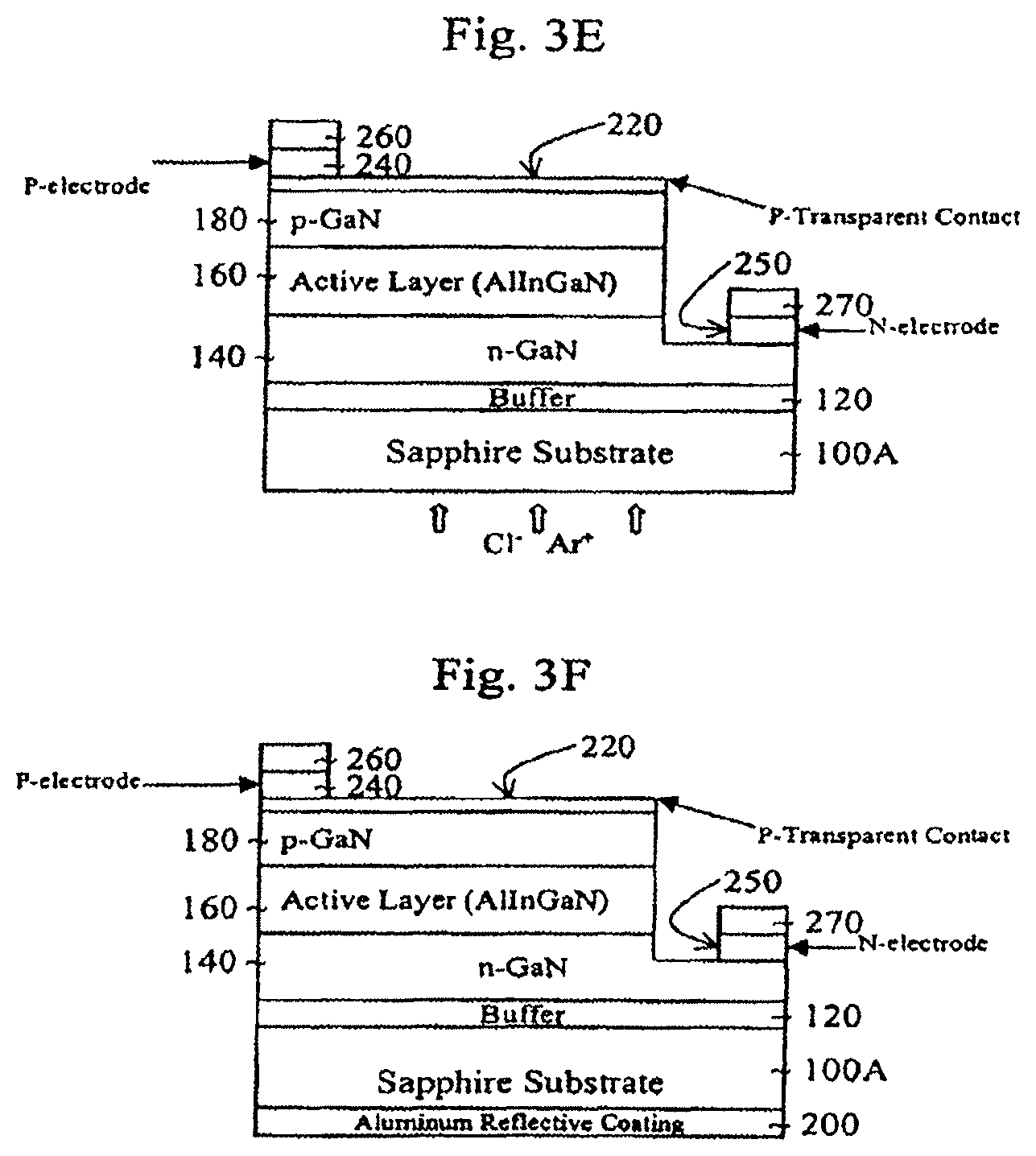
FIGS. 3A-3F illustrate the steps of making a light emitting diode, as an example application of the present invention.
Referring to FIG. 3A, a buffer layer 120 is formed on a substrate 100. The substrate 100 is preferably made from a transparent material including for example, sapphire. In addition to sapphire, the substrate can be made of zinc oxide (ZnO), gallium nitride (GaN), silicon carbide (SiC) and aluminum nitride (AlN). The buffer layer 120 is made of, for example, GaN (Gallium Nitride) and, in this instance, the GaN was grown on the surface of the sapphire substrate 100. An n-type epitaxial layer such as n-GaN 140 is formed on the buffer layer 120. In this instance, the n-GaN layer 140 was doped with silicon (Si) with a doping concentration of about 10.sup.17 cm.sup.-3 or greater. An active layer 160 such as an AlInGaN multiple quantum well layer is formed on the n-GaN layer 140. The active layer 160 may also be formed of a single quantum well layer or a double hetero structure. In this instance, the amount of indium (In) determines whether the diode becomes a green diode or a blue diode. For an LED having blue light, indium in the range of about 22% may be used. For an LED having green light, indium in the range of about 40% may be used. The amount of indium used may be varied depending on the desired wavelength of the blue or green color. Subsequently, a p-GaN layer 180 is formed on the active layer 160. In this instance, the p-GaN layer 180 was doped with magnesium (Mg) with a doping concentration of about 10.sup.17 cm.sup.-3 or greater.
Referring to FIG. 3B, a transparent conductive layer 220 is formed on the p-GaN layer 180. The transparent conductive layer 220 may be made of any suitable material including, for example, Ni/Au or indium-tin-oxide (ITO). A p-type electrode 240 is then formed on one side of the transparent conductive layer 220. The p-type electrode 240 may be made of any suitable material including, for example, Ni/Au, Pd/Au, Pd/Ni and Pt. A pad 260 is formed on the p-type electrode 240. The pad 260 may be made of any suitable material including, for example, Au. The pad 260 may have a thickness of about 5000 .ANG. or higher.
Referring to FIG. 3C, the transparent conductive layer 220, the p-GaN layer 180, the active layer 160 and the n-GaN layer 140 are all etched at one portion to form an n-electrode 250 and pad 270. As shown in FIG. 3C, the n-GaN layer 140 is etched partially so that the n-electrode 250 may be formed on the etched surface of the n-GaN layer 140. The n-electrode 250 may be made of any suitable material including, for example, Ti/Al, Cr/Au and Ti/Au. The pad 270 is a metal and may be made from the same material as the pad 260.
Referring to FIG. 3D, the thickness of the substrate 100, such as made from sapphire, is reduced to form a thinner substrate 100A. In this regard, backside lapping is performed on the sapphire substrate 100 to reduce the wafer thickness. After backside lapping, mechanical polishing is performed to obtain an optically flat surface. After mechanical polishing, the surface roughness (Ra) may be less than about 15 nm. Such polishing technique can reduce the surface roughness up to about 5 nm or slightly less. Such low surface roughness adds to the reflective property of the surface.
In the present invention, the thickness of the substrate 100 can be controlled to be in the range of, for example, 350-430 .mu.m. Moreover, the thickness can be reduced to less than 350 .mu.m and to less than 120 .mu.m. Here, mechanical polishing and dry etching techniques are used. For dry etching, inductively coupled plasma (ICP) reactive ion beam etching (RIE) may be used as an example.
Referring to FIG. 3E, the surface roughness is further reduced to obtain a surface roughness of less than 1 nm. The surface roughness can be reduced from 5 nm up to less than 1 nm by using dry etching. One such dry etching technique is inductively coupled plasma (ICP) reactive ion beam etching (RIE) to obtain an atomically flat surface. The maximum reduction of the surface roughness further enhances the reflectivity of the surface. It is noted that depending on the type of material used for the substrate 100, the surface roughness may be further reduced for maximum reflectivity of the surface.
Referring to FIG. 3F, on the polished thin substrate 100A, a reflective material 200 is formed. The reflective material 200 can be any suitable material that can reflect light. In the present example, an aluminum coating of about 300 nm thick was formed on the polished sapphire surface 100A using an electron beam evaporation technique. Of course, other suitable deposition techniques may be used and different thicknesses of the aluminum are contemplated in the present invention. Here, the aluminum may have a concentration of about 99.999% or higher, which allows the aluminum to have a mirror-like property with maximum light reflectivity. Moreover, the reflective layer 200 entirely covers the second side of the substrate 100A.
FIG. 5 shows an alternative embodiment in which a cladding layer 170 is formed between the p-GaN layer 180 and the active layer 160. The cladding layer 170 is preferably formed with p-AlGaN. The cladding layer 170 enhances the performance of the diode. For simplicity, FIG. 5 does not show the p-electrode, n-electrode and the pads.
As conceptually shown in FIGS. 2A and 2B, the photons generated in the active layer which head toward the polished sapphire surface and the aluminum mirror coating 200 are reflected. Such reflected photons add to the brightness of the diode (photon recovery). Adding the reflective layer and making atomically flat surface greatly increases the brightness of the diode. In addition to the reflective surface of the reflective layer 200, it is important to note that the low surface roughness of the substrate 100 also enhances the photon reflection.
FIG. 6 is a graph showing a relationship between the light output and the injection current of, for example, a light emitting diode (LED). One curve of the graph depicts an LED having a reflective layer (in this case, an aluminum) and the other curve depicts an LED without a reflective layer. In this graph, only mechanical polishing was performed on both LED's. When the reflective aluminum layer was added to the mechanically polished surface of the sapphire substrate, the light output increased about 200% as compared to the device without the reflective layer.
FIG. 4A shows a wafer having LEDs formed thereon. Scribe lines 300 are formed on the wafer through the buffer layer 120 from the side having the LEDs (front scribing) to separate the LED chips. The scribe lines 300 are formed using, for example, a dry etching technique or mechanical scribing. The dry etching technique such as inductively coupled plasma (ICP) reactive ion beam etching (RIE) can form very narrow scribe lines on the buffer layer 120 and the substrate 100A. Using such dry etching technique greatly increased the number of LED chips on the wafer because the space between the chips can be made very small. For example, the space between the diode chips can be as narrow as 10 .mu.m or lower. FIG. 48 is an alternative method of forming the scribe lines in which the back side of the diode used.
The scribe lines may also be formed by a diamond stylus, which requires a large spacing between the diode chips due to the size of the diamond stylus itself. Also, a dicing technique may be used to separate the chips.
Once the diode chips are separated, each diode may be packaged. Such package may also be coated with a reflective material to further enhance the light output.
The present invention applies a simple and inexpensive light extraction process to the existing device fabrication process. According to this invention, adding just one more step of metallization after backside lapping and polishing allows a significant light output increase. With finer polishing using dry etching, in some cases, the light output can be as much as a factor of four without a substantial increase in production cost.
The diode of the present invention improves light intensity of a diode such as an AlInGaN-based light emitting diode (LED) using a reflective coating. The reflective coating recovers those photons, which would otherwise be absorbed by the substrate or the lead frame in the LED package. This increases the total external quantum efficiency of the quantum well devices. This invention can be applied not only to the current commercially available blue, green, red and white LEDs but also to other LED devices. Using this technique, the light output was increased by as much as a factor of four as compared to conventional LED devices (without the reflective coating) without significantly sacrificing or changing other characteristics of the diode.
Although the present invention has been described in detail with reference to GaN technology diodes, the reflector and substrate polishing technique of the present invention can easily be applied to other types of diodes including red LEDs and laser diodes including VCSELs. Although red LEDs do not use GaN, the substrate of the red LEDs may just as easily be polished and a reflective layer can easily be attached to the polished surface of the substrate, as described above. Such technique also recovers the photons to increase the light output of the diode. Similar technique is also applicable for laser diodes.
It will be apparent to those skilled in the art that various modifications and variation can be made in the present invention without departing from the split or scope of the invention. Thus, it is intended that the present invention cover the modifications and variations of this invention provided they come within the scope of the appended claims and their equivalents.
* * * * *
D00000
D00001
D00002
D00003
D00004
D00005
D00006
D00007
D00008
D00009
D00010
XML
uspto.report is an independent third-party trademark research tool that is not affiliated, endorsed, or sponsored by the United States Patent and Trademark Office (USPTO) or any other governmental organization. The information provided by uspto.report is based on publicly available data at the time of writing and is intended for informational purposes only.
While we strive to provide accurate and up-to-date information, we do not guarantee the accuracy, completeness, reliability, or suitability of the information displayed on this site. The use of this site is at your own risk. Any reliance you place on such information is therefore strictly at your own risk.
All official trademark data, including owner information, should be verified by visiting the official USPTO website at www.uspto.gov. This site is not intended to replace professional legal advice and should not be used as a substitute for consulting with a legal professional who is knowledgeable about trademark law.