Back-surface-incident type light-receiving device and optical module
Takemura , et al. Fe
U.S. patent number 10,553,742 [Application Number 16/306,788] was granted by the patent office on 2020-02-04 for back-surface-incident type light-receiving device and optical module. This patent grant is currently assigned to Mitsubishi Electric Corporation. The grantee listed for this patent is Mitsubishi Electric Corporation. Invention is credited to Nobuo Ohata, Yoshifumi Sasahata, Ryota Takemura, Kazuki Yamaji.


| United States Patent | 10,553,742 |
| Takemura , et al. | February 4, 2020 |
Back-surface-incident type light-receiving device and optical module
Abstract
A substrate has a front surface and a back surface opposite from the front surface. An n-type layer, a multiplication layer, a p-type electric field control layer, a light absorption layer, and a window layer are layered in order on the front surface. A p-type region is provided in part of the window layer. An anode electrode is provided on the p-type region and connected to the p-type region. An anode pad and a cathode pad are provided on the back surface. First and second connecting holes penetrates the substrate. A third connecting hole penetrates from the window layer to the n-type layer. The cathode pad is electrically connected to the n-type layer via the first connecting hole. The anode pad is electrically connected to the anode electrode via the second and third connecting holes. A light-receiving region is provided on the back surface.
| Inventors: | Takemura; Ryota (Tokyo, JP), Ohata; Nobuo (Tokyo, JP), Sasahata; Yoshifumi (Tokyo, JP), Yamaji; Kazuki (Tokyo, JP) | ||||||||||
|---|---|---|---|---|---|---|---|---|---|---|---|
| Applicant: |
|
||||||||||
| Assignee: | Mitsubishi Electric Corporation
(Tokyo, JP) |
||||||||||
| Family ID: | 62024625 | ||||||||||
| Appl. No.: | 16/306,788 | ||||||||||
| Filed: | October 28, 2016 | ||||||||||
| PCT Filed: | October 28, 2016 | ||||||||||
| PCT No.: | PCT/JP2016/082033 | ||||||||||
| 371(c)(1),(2),(4) Date: | December 03, 2018 | ||||||||||
| PCT Pub. No.: | WO2018/078788 | ||||||||||
| PCT Pub. Date: | May 03, 2018 |
Prior Publication Data
| Document Identifier | Publication Date | |
|---|---|---|
| US 20190296175 A1 | Sep 26, 2019 | |
| Current U.S. Class: | 1/1 |
| Current CPC Class: | H01L 31/022408 (20130101); H01L 31/109 (20130101); G01J 1/44 (20130101); H01L 31/03046 (20130101); H01L 31/1075 (20130101); H01L 31/0203 (20130101); H01L 31/10 (20130101) |
| Current International Class: | H01L 31/109 (20060101); H01L 31/0224 (20060101); G01J 1/44 (20060101) |
| Field of Search: | ;257/184 |
References Cited [Referenced By]
U.S. Patent Documents
| 9257577 | February 2016 | Kikuchi et al. |
| 10274687 | April 2019 | Shi |
| 2005/0230706 | October 2005 | Yagyu |
| 2006/0186501 | August 2006 | Ishimura |
| 2006/0202297 | September 2006 | Ishimura |
| 2009/0289316 | November 2009 | Ishimura |
| 2009/0294787 | December 2009 | Nakaji |
| 2011/0073973 | March 2011 | Nakaji |
| 2013/0193546 | August 2013 | Webster |
| 2013/0200477 | August 2013 | Sun |
| 2014/0167200 | June 2014 | Sun |
| 2015/0270814 | September 2015 | Ban et al. |
| 2016/0126381 | May 2016 | Wang |
| 2019/0013430 | January 2019 | Jones-Albertus |
| 2019/0019899 | January 2019 | Wang |
| 2019/0259900 | August 2019 | Furuyama |
| 2019/0288132 | September 2019 | Wang |
| 2011-253904 | Dec 2011 | JP | |||
| 2014-192510 | Oct 2014 | JP | |||
Other References
|
International Search Report issued in PCT/JP2016/082033; dated Dec. 20, 2016. cited by applicant . Written Opinion issued in PCT/JP2016/082033; dated Dec. 20, 2016. cited by applicant . Notification of Transmittal of the International Search Report and the Written Opinion of the International Searching Authority, or the Declaration issued in PCT/JP2016/082033; dated Dec. 20, 2016. cited by applicant. |
Primary Examiner: Williams; Alexander O
Attorney, Agent or Firm: Studebaker & Brackett PC
Claims
The invention claimed is:
1. A back-surface-incident type light-receiving device comprising: a substrate having a front surface and a back surface opposite from the front surface; an n-type layer, a multiplication layer, a p-type electric field control layer, a light absorption layer, and a window layer which are layered in order on the front surface; a p-type region provided in part of the window layer; an anode electrode provided on the p-type region and connected to the p-type region; and an anode pad and a cathode pad which are provided on the back surface, wherein first and second connecting holes penetrate the substrate, a third connecting hole penetrates from the window layer to the n-type layer, the cathode pad is electrically connected to the n-type layer via the first connecting hole, the anode pad is electrically connected to the anode electrode via the second and third connecting holes, and a light-receiving region is provided on the back surface.
2. The back-surface-incident type light-receiving device according to claim 1, wherein an etched hole penetrates from the window layer to the n-type layer and is embedded with a semi-insulating layer, and the third connecting hole is provided in the semi-insulating layer.
3. The back-surface-incident type light-receiving device according to claim 1, further comprising an etch stop layer inserted between the n-type layer and the multiplication layer.
4. The back-surface-incident type light-receiving device according to claim 1, wherein the second and third connecting holes continuously penetrate from the substrate to the window layer.
5. The back-surface-incident type light-receiving device according to claim 1, further comprising an insulating film provided between the substrate and the anode and cathode pads, wherein the substrate is a conductive substrate.
6. An optical module comprising: a submount; the back-surface-incident type light-receiving device according to claim 1 fixed on the submount with the light-receiving region facing upward; first and second circuit components; a first wire connecting the cathode pad to the first circuit component; and a second wire connecting the anode pad to the second circuit component.
7. The back-surface-incident type light-receiving device according to claim 2, further comprising an etch stop layer inserted between the n-type layer and the multiplication layer.
8. The back-surface-incident type light-receiving device according to claim 2, further comprising an insulating film provided between the substrate and the anode and cathode pads, wherein the substrate is a conductive substrate.
9. The back-surface-incident type light-receiving device according to claim 3, further comprising an insulating film provided between the substrate and the anode and cathode pads, wherein the substrate is a conductive substrate.
10. The back-surface-incident type light-receiving device according to claim 7, further comprising an insulating film provided between the substrate and the anode and cathode pads, wherein the substrate is a conductive substrate.
11. The back-surface-incident type light-receiving device according to claim 4, further comprising an insulating film provided between the substrate and the anode and cathode pads, wherein the substrate is a conductive substrate.
Description
FIELD
The present invention relates to a back-surface-incident type light-receiving device and an optical module used for optical fiber communications and the like.
BACKGROUND
The structures of semiconductor light-receiving devices are roughly classified into: a front-surface-incident type that receives light incident from a front surface of an epitaxial growth layer on a semiconductor substrate; an end-face-incident type that receives light incident from a side face of the epitaxial growth layer; and a back-surface-incident type that receives light incident from a back surface of a semiconductor substrate.
Generally, a semiconductor light-receiving device can sense light only in a p-n junction region. A larger p-n junction region can more easily adjust the optical axis and provides good mountability. On the other hand, the device capacitance increases with the size of the p-n junction region, which is not advantageous in respect of high-speed response because of increased time constant.
Since back-surface-incident type light-receiving devices can readily be designed with low parasitic capacitance, the p-n joint region can be made accordingly larger, which makes it feasible to achieve both of easy mountability and high-speed operation enabled by reduction of device capacitance. The back-surface-incident type is therefore a commonly used structure for high-speed communications, in particular with a rate of 10 Gbps or more. Moreover, a high quantum efficiency is easier to achieve with a back-surface-incident type light-receiving device because light incident from the backside of the substrate is reflected by electrode metal mirrors back to an absorption layer to be absorbed again. Optical modules using such back-surface-incident type light-receiving devices have been disclosed (see, for example, PTL 1 and PTL 2).
CITATION LIST
Patent Literature
[PTL 1] Japanese Patent Application Laid-open No. 2014-192510
[PTL 2] Japanese Patent Application Laid-open No. 2011-253904
SUMMARY
Technical Problem
Since anodes and cathodes of back-surface-incident type light-receiving devices are formed on the front surface of the substrate, the anodes and cathodes are die-bonded to metal patterns formed on a submount using solder, Au bumps or the like, with wires provided to respective metal patterns. One problem here was that the necessity to form the patterns for the wires on the submount increased the size of the submount.
Another problem was that Au wires connecting other circuit components such as TIAs and capacitors with the back-surface-incident type light-receiving device extend over wiring patterns on the submount that has a different dielectric constant, because of which high-frequency reflection points were increased, causing resonance and lowering reception sensitivity.
The present invention was made to solve the problems described above and it is an object of the invention to provide a back-surface-incident type light-receiving device and an optical module that enable size reduction to improve reception sensitivity.
Solution to Problem
A back-surface-incident type light-receiving device according to the present invention includes: a substrate having a front surface and a back surface opposite from the front surface; an n-type layer, a multiplication layer, a p-type electric field control layer, a light absorption layer, and a window layer which are layered in order on the front surface; a p-type region provided in part of the window layer; an anode electrode provided on the p-type region and connected to the p-type region; and an anode pad and a cathode pad which are provided on the back surface, wherein first and second connecting holes penetrate the substrate, a third connecting hole penetrates from the window layer to the n-type layer, the cathode pad is electrically connected to the n-type layer via the first connecting hole, the anode pad is electrically connected to the anode electrode via the second and third connecting holes, and a light-receiving region is provided on the back surface.
Advantageous Effects of Invention
The present invention has the anode pad and cathode pad on the back surface of the substrate, so that the wires for connecting them to other circuit components can be directly formed on the back surface of the substrate of the back-surface-incident type light-receiving device. Patterns on the submount are therefore not necessary, so that the submount can be made smaller. Since there are no high frequency reflection points, resonance hardly occurs, and accordingly the reception sensitivity can be improved.
BRIEF DESCRIPTION OF THE DRAWINGS
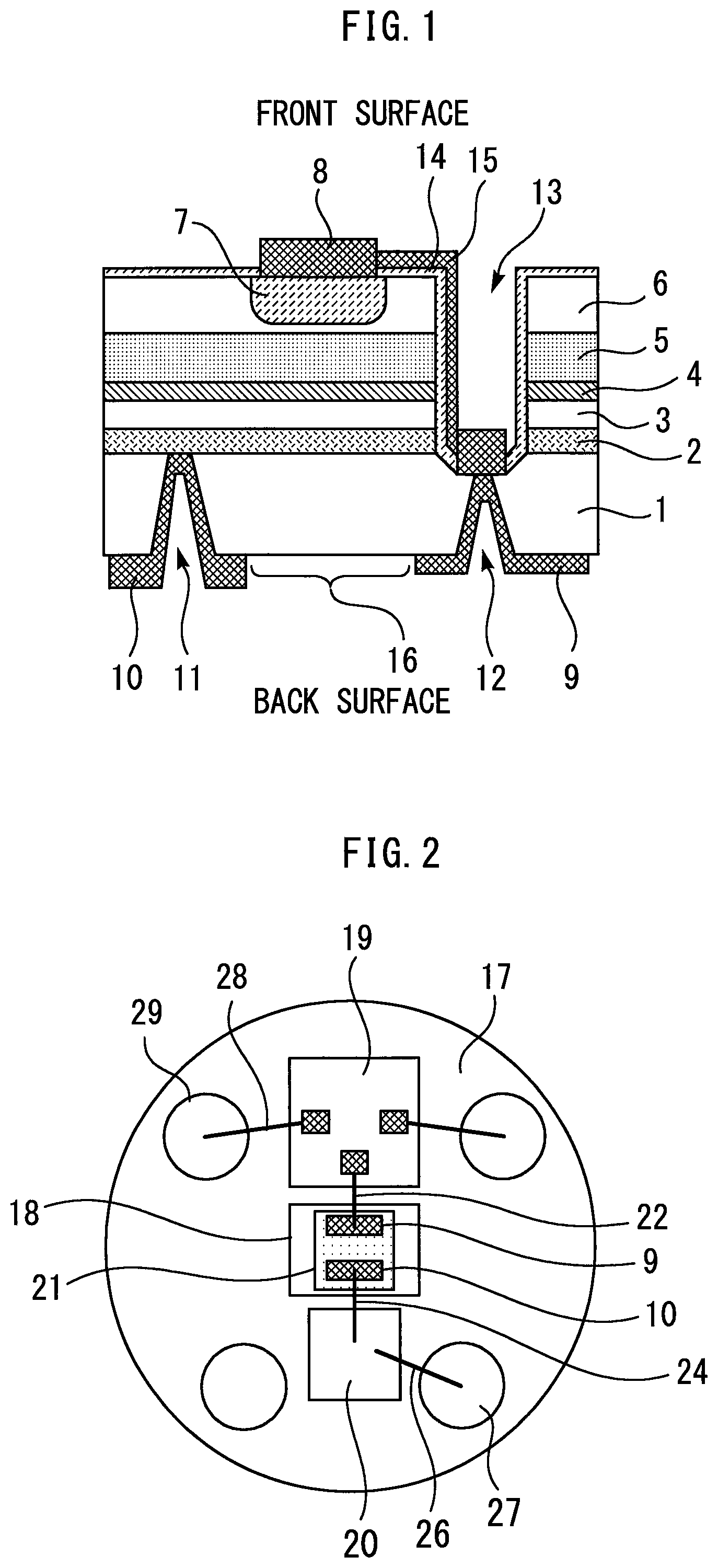
FIG. 1 is a cross-sectional view illustrating a back-surface-incident type light-receiving device according to Embodiment 1 of the present invention.
FIG. 2 is a plan view illustrating an optical module according to Embodiment 1 of the present invention.
FIG. 3 is a perspective view illustrating major parts of the optical module according to Embodiment 1 of the present invention.
FIG. 4 is a perspective view illustrating an optical module that uses a back-surface-incident type light-receiving device of a comparative example.
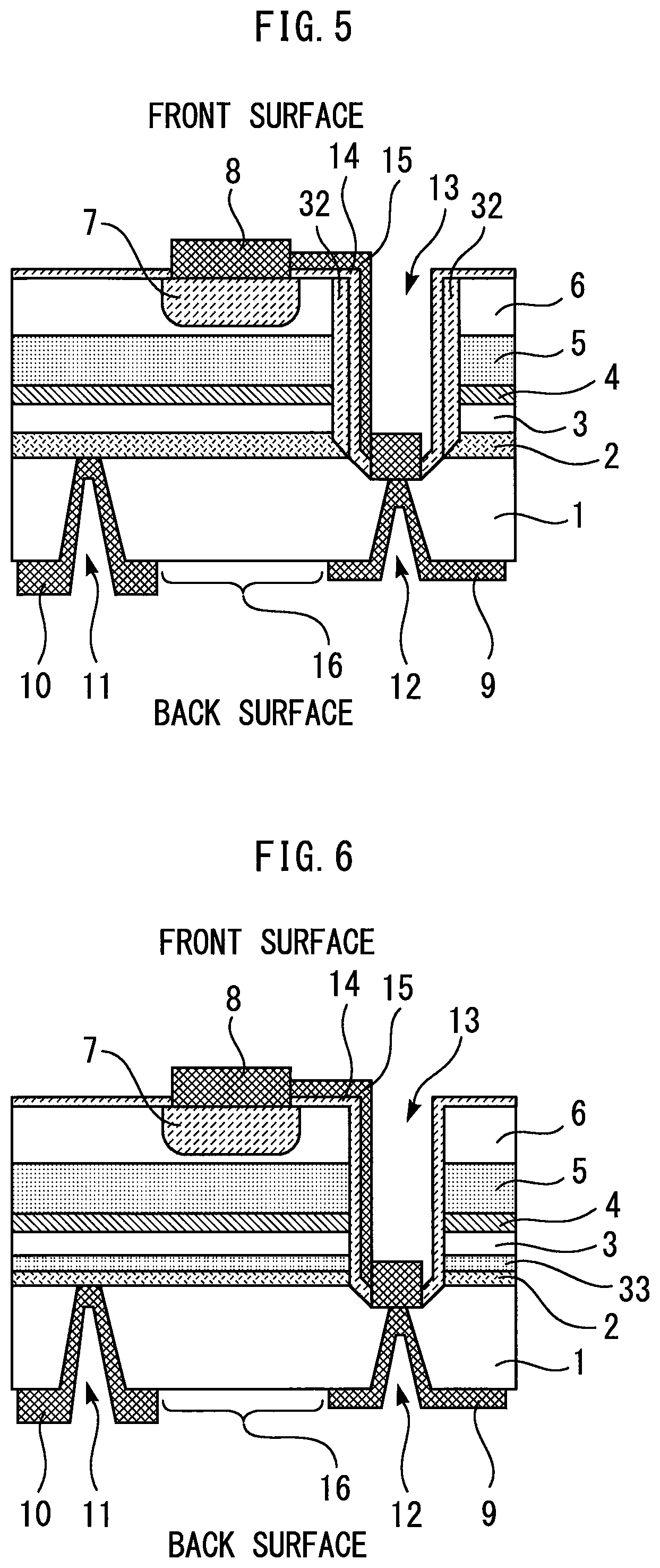
FIG. 5 is a cross-sectional view illustrating a back-surface-incident type light-receiving device according to Embodiment 2 of the present invention.
FIG. 6 is a cross-sectional view illustrating a back-surface-incident type light-receiving device according to Embodiment 3 of the present invention.
FIG. 7 is a cross-sectional view illustrating a back-surface-incident type light-receiving device according to Embodiment 4 of the present invention.
FIG. 8 is a cross-sectional view illustrating a back-surface-incident type light-receiving device according to Embodiment 5 of the present invention.
DESCRIPTION OF EMBODIMENTS
A back-surface-incident type light-receiving device and an optical module according to the embodiments of the present invention will be described with reference to the drawings. The same components will be denoted by the same symbols, and the repeated description thereof may be omitted.
Embodiment 1
FIG. 1 is a cross-sectional view illustrating a back-surface-incident type light-receiving device according to Embodiment 1 of the present invention. The substrate 1 is a semi-insulating InP substrate having a front surface and a back surface opposite from the front surface. An n-type layer 2, an AlInAs multiplication layer 3, an InP p-type electric field control layer 4, an InGaAs light absorption layer 5, and an InP window layer 6 are layered in order on the front surface of the substrate 1. A p-type region 7 is formed in part of the window layer 6. An anode electrode 8 is formed on the p-type region 7 and connected to the p-type region 7.
An anode pad 9 and a cathode pad 10 are formed on the back surface of the substrate 1. First and second connecting holes 11 and 12 penetrating the substrate 1 are formed by etching. A third connecting hole 13 penetrating from the window layer 6 to the n-type layer 2 is formed by etching such as to be connected at least partly to the second connecting hole 12. An upper surface of the InP window layer 6 and inner side faces of the third connecting hole 13 are covered by a passivation film 14 of SiN or the like.
The cathode pad 10 is electrically connected to the n-type layer 2 via the first connecting hole 11. The anode pad 9 is electrically connected to the anode electrode 8 via anode wiring 15 inside the second connecting hole 12 and the third connecting hole 13. The substrate 1 has a light-receiving region 16 on the back surface in the area other than the anode pad 9 and the cathode pad 10.
FIG. 2 is a plan view illustrating an optical module according to Embodiment 1 of the present invention. FIG. 3 is a perspective view illustrating major parts of the optical module according to Embodiment 1 of the present invention. A submount 18, TIA (transimpedance amplifier) 19, and a capacitor 20 are fixed with solder on a can package carrier 17. The back-surface-incident type light-receiving device 21 is fixed on the submount 18 with its light-receiving region 16 facing upward. The anode pad 9 is connected to a bonding pad 23 of the TIA 19 via an Au wire 22. The cathode pad 10 is connected to a bonding pad 25 of the capacitor 20 via an Au wire 24. The capacitor 20 is connected to a lead terminal 27 via an Au wire 26. The TIA 19 is connected to a lead terminal 29 via an Au wire 28. The design is not limited to this and the cathode pad 10 and anode pad 9 of the back-surface-incident type light-receiving device 21 may be connected to other circuit components such as resistors or lead terminals.
Next, the effects of this embodiment will be explained in comparison to a comparative example. FIG. 4 is a perspective view illustrating an optical module that uses a back-surface-incident type light-receiving device of a comparative example. The anode and cathode of the back-surface-incident type light-receiving device 21 according to the comparative example are formed on the front surface of the substrate. Therefore, metal patterns 30 and 31 need to be formed on the submount 18 to provide wires extending from the anode and cathode, so that the submount 18 has to have a larger size. High frequency reflection points are accordingly increased, which cause resonance and lower the reception sensitivity.
On the other hand, the back-surface-incident type light-receiving device 21 according to this embodiment has the anode pad 9 and cathode pad 10 on the back surface of the substrate, so that the wires for connecting them to other circuit components can be directly formed on the back surface of the substrate of the back-surface-incident type light-receiving device 21. Patterns on the submount 18 are therefore not necessary, so that the submount 18 can be made smaller. Since there are no high frequency reflection points, resonance hardly occurs, and accordingly the reception sensitivity can be improved.
The p-type electric field control layer 4 may be made of AlInAs. The light absorption layer 5 may be made of InGaAsP or the like instead of InGaAs, as long as the material has a small band gap relative to the incident light. The window layer 6 may be made of AlInAs, AlGaInAs, InGaAsP and the like, as long as the material has a large band gap relative to the incident light. A layer of AlGaInAs, InGaAsP, InGaAs or the like may be provided between the p-type region 7 and the anode electrode 8 in order to reduce contact resistance. The light-receiving region 16 may partly be provided with an anti-reflection (AR) coating which is an insulating film or the like. Any materials may be used for each of the layers for achieving characteristics necessary for the operation. The materials mentioned above shall not limit the scope of the present invention. The p-type region 7 may be formed by thermal diffusion, ion injection and the like, but the forming method is not limited particularly.
Embodiment 2
FIG. 5 is a cross-sectional view illustrating a back-surface-incident type light-receiving device according to Embodiment 2 of the present invention. The etched hole penetrates from the light absorption layer to the n-type layer and is embedded with a semi-insulating layer 32 containing Fe--InP or Ru--InP. The third connecting hole 13 is formed in the semi-insulating layer 32. This makes the distance between the anode wiring 15 and the semiconductor layer wider, so that reliability is improved. Other configurations and effects are similar to those of Embodiment 1.
Embodiment 3
FIG. 6 is a cross-sectional view illustrating a back-surface-incident type light-receiving device according to Embodiment 3 of the present invention. An etch stop layer 33 that is not InP is inserted between the n-type layer 2 and the multiplication layer 3. This allows for selective etching when forming the second connecting hole 12 by etching from the substrate side, and when forming the third connecting hole 13 by etching from the epitaxial surface side. Thus the second and third connecting holes 12 and 13 can be readily formed. Other configurations and effects are similar to those of Embodiment 1.
Embodiment 4
FIG. 7 is a cross-sectional view illustrating a back-surface-incident type light-receiving device according to Embodiment 4 of the present invention. An insulating film 34 is formed between the substrate 1 and the anode and cathode pads 9 and 10. This allows the substrate 1 to have any polarities, so that a conductive substrate can be used. Also, the anode pad 9 and cathode pad 10 can be formed without being affected by the polarity of the substrate, which makes the fabrication easy. Other configurations and effects are similar to those of Embodiment 3.
Embodiment 5
FIG. 8 is a cross-sectional view illustrating a back-surface-incident type light-receiving device according to Embodiment 5 of the present invention. The second and third connecting holes 12 and 13 continuously penetrate from the substrate 1 to the window layer 6. This eliminates the need to etch both sides of the substrate, which makes the fabrication easy. Other configurations and effects are similar to those of Embodiment 1.
REFERENCE SIGNS LIST
1 substrate; 2 n-type layer; 3 multiplication layer; 4 p-type electric field control layer; 5 light absorption layer; 6 window layer; 7 p-type region; 8 anode electrode; 9 anode pad; 10 cathode pad; 11 first connecting hole; 12 second connecting hole; 13 third connecting hole; 16 light-receiving region; 18 submount; 19 TIA (second circuit component); 20 capacitor (first circuit component); 21 back-surface-incident type light-receiving device; 22 Au wire (second wire); 24 Au wire (first wire); 32 semi-insulating layer; 33 etch stop layer; 34 insulating film
* * * * *
D00000
D00001
D00002
D00003
D00004
XML
uspto.report is an independent third-party trademark research tool that is not affiliated, endorsed, or sponsored by the United States Patent and Trademark Office (USPTO) or any other governmental organization. The information provided by uspto.report is based on publicly available data at the time of writing and is intended for informational purposes only.
While we strive to provide accurate and up-to-date information, we do not guarantee the accuracy, completeness, reliability, or suitability of the information displayed on this site. The use of this site is at your own risk. Any reliance you place on such information is therefore strictly at your own risk.
All official trademark data, including owner information, should be verified by visiting the official USPTO website at www.uspto.gov. This site is not intended to replace professional legal advice and should not be used as a substitute for consulting with a legal professional who is knowledgeable about trademark law.